JP7011161B2 - Display device - Google Patents
Display device Download PDFInfo
- Publication number
- JP7011161B2 JP7011161B2 JP2018015517A JP2018015517A JP7011161B2 JP 7011161 B2 JP7011161 B2 JP 7011161B2 JP 2018015517 A JP2018015517 A JP 2018015517A JP 2018015517 A JP2018015517 A JP 2018015517A JP 7011161 B2 JP7011161 B2 JP 7011161B2
- Authority
- JP
- Japan
- Prior art keywords
- array
- display device
- electrodes
- image
- substrate
- Prior art date
- Legal status (The legal status is an assumption and is not a legal conclusion. Google has not performed a legal analysis and makes no representation as to the accuracy of the status listed.)
- Active
Links
Images


Classifications
-
- G—PHYSICS
- G02—OPTICS
- G02B—OPTICAL ELEMENTS, SYSTEMS OR APPARATUS
- G02B3/00—Simple or compound lenses
- G02B3/0006—Arrays
-
- G—PHYSICS
- G02—OPTICS
- G02F—OPTICAL DEVICES OR ARRANGEMENTS FOR THE CONTROL OF LIGHT BY MODIFICATION OF THE OPTICAL PROPERTIES OF THE MEDIA OF THE ELEMENTS INVOLVED THEREIN; NON-LINEAR OPTICS; FREQUENCY-CHANGING OF LIGHT; OPTICAL LOGIC ELEMENTS; OPTICAL ANALOGUE/DIGITAL CONVERTERS
- G02F1/00—Devices or arrangements for the control of the intensity, colour, phase, polarisation or direction of light arriving from an independent light source, e.g. switching, gating or modulating; Non-linear optics
- G02F1/01—Devices or arrangements for the control of the intensity, colour, phase, polarisation or direction of light arriving from an independent light source, e.g. switching, gating or modulating; Non-linear optics for the control of the intensity, phase, polarisation or colour
- G02F1/13—Devices or arrangements for the control of the intensity, colour, phase, polarisation or direction of light arriving from an independent light source, e.g. switching, gating or modulating; Non-linear optics for the control of the intensity, phase, polarisation or colour based on liquid crystals, e.g. single liquid crystal display cells
- G02F1/133—Constructional arrangements; Operation of liquid crystal cells; Circuit arrangements
- G02F1/1333—Constructional arrangements; Manufacturing methods
- G02F1/1335—Structural association of cells with optical devices, e.g. polarisers or reflectors
- G02F1/133526—Lenses, e.g. microlenses or Fresnel lenses
-
- G—PHYSICS
- G02—OPTICS
- G02B—OPTICAL ELEMENTS, SYSTEMS OR APPARATUS
- G02B27/00—Optical systems or apparatus not provided for by any of the groups G02B1/00 - G02B26/00, G02B30/00
- G02B27/09—Beam shaping, e.g. changing the cross-sectional area, not otherwise provided for
- G02B27/0938—Using specific optical elements
- G02B27/095—Refractive optical elements
- G02B27/0955—Lenses
- G02B27/0961—Lens arrays
-
- G—PHYSICS
- G02—OPTICS
- G02B—OPTICAL ELEMENTS, SYSTEMS OR APPARATUS
- G02B30/00—Optical systems or apparatus for producing three-dimensional [3D] effects, e.g. stereoscopic images
- G02B30/20—Optical systems or apparatus for producing three-dimensional [3D] effects, e.g. stereoscopic images by providing first and second parallax images to an observer's left and right eyes
- G02B30/26—Optical systems or apparatus for producing three-dimensional [3D] effects, e.g. stereoscopic images by providing first and second parallax images to an observer's left and right eyes of the autostereoscopic type
- G02B30/27—Optical systems or apparatus for producing three-dimensional [3D] effects, e.g. stereoscopic images by providing first and second parallax images to an observer's left and right eyes of the autostereoscopic type involving lenticular arrays
-
- G—PHYSICS
- G02—OPTICS
- G02B—OPTICAL ELEMENTS, SYSTEMS OR APPARATUS
- G02B30/00—Optical systems or apparatus for producing three-dimensional [3D] effects, e.g. stereoscopic images
- G02B30/50—Optical systems or apparatus for producing three-dimensional [3D] effects, e.g. stereoscopic images the image being built up from image elements distributed over a 3D volume, e.g. voxels
- G02B30/56—Optical systems or apparatus for producing three-dimensional [3D] effects, e.g. stereoscopic images the image being built up from image elements distributed over a 3D volume, e.g. voxels by projecting aerial or floating images
-
- G—PHYSICS
- G02—OPTICS
- G02B—OPTICAL ELEMENTS, SYSTEMS OR APPARATUS
- G02B5/00—Optical elements other than lenses
- G02B5/02—Diffusing elements; Afocal elements
-
- G—PHYSICS
- G02—OPTICS
- G02F—OPTICAL DEVICES OR ARRANGEMENTS FOR THE CONTROL OF LIGHT BY MODIFICATION OF THE OPTICAL PROPERTIES OF THE MEDIA OF THE ELEMENTS INVOLVED THEREIN; NON-LINEAR OPTICS; FREQUENCY-CHANGING OF LIGHT; OPTICAL LOGIC ELEMENTS; OPTICAL ANALOGUE/DIGITAL CONVERTERS
- G02F1/00—Devices or arrangements for the control of the intensity, colour, phase, polarisation or direction of light arriving from an independent light source, e.g. switching, gating or modulating; Non-linear optics
- G02F1/01—Devices or arrangements for the control of the intensity, colour, phase, polarisation or direction of light arriving from an independent light source, e.g. switching, gating or modulating; Non-linear optics for the control of the intensity, phase, polarisation or colour
- G02F1/13—Devices or arrangements for the control of the intensity, colour, phase, polarisation or direction of light arriving from an independent light source, e.g. switching, gating or modulating; Non-linear optics for the control of the intensity, phase, polarisation or colour based on liquid crystals, e.g. single liquid crystal display cells
- G02F1/133—Constructional arrangements; Operation of liquid crystal cells; Circuit arrangements
- G02F1/1333—Constructional arrangements; Manufacturing methods
- G02F1/1335—Structural association of cells with optical devices, e.g. polarisers or reflectors
- G02F1/133504—Diffusing, scattering, diffracting elements
-
- G—PHYSICS
- G02—OPTICS
- G02F—OPTICAL DEVICES OR ARRANGEMENTS FOR THE CONTROL OF LIGHT BY MODIFICATION OF THE OPTICAL PROPERTIES OF THE MEDIA OF THE ELEMENTS INVOLVED THEREIN; NON-LINEAR OPTICS; FREQUENCY-CHANGING OF LIGHT; OPTICAL LOGIC ELEMENTS; OPTICAL ANALOGUE/DIGITAL CONVERTERS
- G02F1/00—Devices or arrangements for the control of the intensity, colour, phase, polarisation or direction of light arriving from an independent light source, e.g. switching, gating or modulating; Non-linear optics
- G02F1/01—Devices or arrangements for the control of the intensity, colour, phase, polarisation or direction of light arriving from an independent light source, e.g. switching, gating or modulating; Non-linear optics for the control of the intensity, phase, polarisation or colour
- G02F1/13—Devices or arrangements for the control of the intensity, colour, phase, polarisation or direction of light arriving from an independent light source, e.g. switching, gating or modulating; Non-linear optics for the control of the intensity, phase, polarisation or colour based on liquid crystals, e.g. single liquid crystal display cells
- G02F1/133—Constructional arrangements; Operation of liquid crystal cells; Circuit arrangements
- G02F1/1333—Constructional arrangements; Manufacturing methods
- G02F1/1343—Electrodes
-
- G—PHYSICS
- G02—OPTICS
- G02F—OPTICAL DEVICES OR ARRANGEMENTS FOR THE CONTROL OF LIGHT BY MODIFICATION OF THE OPTICAL PROPERTIES OF THE MEDIA OF THE ELEMENTS INVOLVED THEREIN; NON-LINEAR OPTICS; FREQUENCY-CHANGING OF LIGHT; OPTICAL LOGIC ELEMENTS; OPTICAL ANALOGUE/DIGITAL CONVERTERS
- G02F1/00—Devices or arrangements for the control of the intensity, colour, phase, polarisation or direction of light arriving from an independent light source, e.g. switching, gating or modulating; Non-linear optics
- G02F1/29—Devices or arrangements for the control of the intensity, colour, phase, polarisation or direction of light arriving from an independent light source, e.g. switching, gating or modulating; Non-linear optics for the control of the position or the direction of light beams, i.e. deflection
- G02F1/294—Variable focal length devices
Description
本開示は、表示装置に関する。 The present disclosure relates to a display device.
インテグラルフォトグラフィの原理に基づく画像生成技術であるインテグラルイメージングが知られている。インテグラルイメージングは、複数の要素画像から、視認される一つの再生像(視認像)を形成する。インテグラルイメージングを行う典型的な表示システムは、ディスプレイ上に、再生像が縮小された複数の要素画像を表示する。表示システムは、複数の要素画像からの光を、複数の要素画像それぞれに対応するマイクロレンズ(要素レンズ)からなるマイクロレンズアレイを通して照射することで、ディスプレイから離れた空中における特定の位置に再生像を形成する。 Integral imaging, which is an image generation technique based on the principle of integral photography, is known. Integral imaging forms one reproduced image (visual image) that is visually recognized from a plurality of element images. A typical display system for integral imaging displays a plurality of element images in which a reproduced image is reduced on a display. The display system irradiates light from a plurality of element images through a microlens array consisting of microlenses (element lenses) corresponding to each of the plurality of element images, thereby reproducing a reproduced image at a specific position in the air away from the display. To form.
上記従来の表示システムにおいて再生像の解像度を上げるためには、解像度の高い微小な要素画像が必要になる。つまり、高精細なディスプレイが必要とされる。しかし、ディスプレイの精細化には限界があり、高解像度な再生像の形成には限界がある。 In order to increase the resolution of the reproduced image in the above-mentioned conventional display system, a minute element image having a high resolution is required. That is, a high-definition display is required. However, there is a limit to the fineness of the display, and there is a limit to the formation of a high-resolution reproduced image.
本開示の一態様は、元画像を元画像表示位置に表示する表示デバイスと、レンズアレイ又はピンホールアレイである、第2アレイと、前記表示デバイスと前記第2アレイとの間に、前記表示デバイス及び前記第2アレイから離間して配置された、レンズアレイ又はピンホールアレイである、第1アレイと、を含み、前記第1アレイは、前記元画像から生成した複数の要素画像を、前記第1アレイと前記第2アレイとの間に結像し、前記複数の要素画像のピッチは、前記第2アレイのレンズピッチ又はピンホールピッチと異なり、前記第2アレイは、前記複数の要素画像を統合して、前記元画像を表す一つの再生像を生成する、表示装置である。 One aspect of the present disclosure is the display between a display device that displays the original image at the original image display position, a second array that is a lens array or a pinhole array, and the display device and the second array. The first array includes a first array, which is a lens array or a pinhole array, arranged apart from the device and the second array, wherein the first array is a plurality of element images generated from the original image. An image is formed between the first array and the second array, and the pitch of the plurality of element images is different from the lens pitch or pinhole pitch of the second array, and the second array is the plurality of element images. Is a display device that integrates the above to generate one reproduced image representing the original image.
本開示の一態様によれば、元画像を表示する表示装置から離れた位置に、高解像度の視認像を形成することができる。 According to one aspect of the present disclosure, a high-resolution visual image can be formed at a position away from the display device displaying the original image.
以下において、図面を参照して実施形態を具体的に説明する。各図において共通の構成については同一の参照符号が付されている。説明をわかりやすくするため、図示した物の寸法、形状については、誇張して記載している場合もある。 Hereinafter, embodiments will be specifically described with reference to the drawings. The same reference numerals are given to the common configurations in each figure. In order to make the explanation easier to understand, the dimensions and shape of the illustrated object may be exaggerated.
以下において、表示されている元画像から視認される再生像を、元画像と異なる位置に表示する表示装置を開示する。表示装置は、元画像を表示する表示デバイスと、第1及び第2のレンズアレイを含む。第1レンズアレイは、表示デバイスと第2レンズアレイとの間に配置されている。第1レンズアレイは、元画像から複数の要素画像を生成し、第1レンズアレイと第2レンズアレイとの間に結像させる。第2レンズアレイは、複数の要素画像を統合して、一つの再生像を形成する。これにより、元画像と異なる位置に再生像を形成することができる。また、表示デバイスは複数の要素画像ではなく、一つの元画像を表示すればよいので、高解像度の再生像を形成することができる。 Hereinafter, a display device for displaying a reproduced image visually recognized from the displayed original image at a position different from that of the original image will be disclosed. The display device includes a display device for displaying the original image and first and second lens arrays. The first lens array is arranged between the display device and the second lens array. The first lens array generates a plurality of element images from the original image and forms an image between the first lens array and the second lens array. The second lens array integrates a plurality of element images to form one reproduced image. As a result, the reproduced image can be formed at a position different from the original image. Further, since the display device may display one original image instead of a plurality of element images, a high-resolution reproduced image can be formed.
[実施形態1]
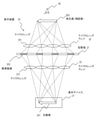
図1Aは、本実施形態に係る表示装置20に含まれる構成要素を模式的に示す分解斜視図である。表示装置20は、表示デバイス21と、第1マイクロレンズアレイ23と、拡散板27と、第2マイクロレンズアレイ25とを含む。ユーザ50は、表示装置20が生成する再生像(視認像)203を視認する。ユーザ50は、表示装置20の前から、再生像203を視る。つまり、ユーザ側が表示装置20の前側であり、その反対側は後側である。
[Embodiment 1]
FIG. 1A is an exploded perspective view schematically showing a component included in the
図1Aに示すように、表示デバイス21の前に第1マイクロレンズアレイ23が配置され、第1マイクロレンズアレイ23の前に拡散板27が配置され、拡散板27の前に第2マイクロレンズアレイ25が配置されている。拡散板27は、第1マイクロレンズアレイ23と第2マイクロレンズアレイ25との間に挟まれた位置にある。
As shown in FIG. 1A, the
表示デバイス21は、例えば、液晶表示デバイス又はOLED(Organic Light Emitting Diode)表示デバイスである。表示デバイス21の種類は問わない。表示デバイス21は、例えば、マトリックス状に配置された複数の画素を含む表示パネルと、表示パネルの画素を駆動する駆動回路及びその制御回路を含む。
The
第1マイクロレンズアレイ23及び第2マイクロレンズアレイ25は、それぞれ、マトリックス状に配置された複数のマイクロレンズ(要素レンズ)を含む。マイクロレンズは、例えば、両凸レンズ又は半凸レンズである。マイクロレンズの外形は、設計により適切に設計され、例えば、矩形又は円である。マイクロレンズアレイ23、25は、例えば、樹脂又はガラスで形成されている。
The
第1マイクロレンズアレイ23は、表示デバイス21から離間して配置されている。拡散板27は、第1マイクロレンズアレイ23から離間して又は接触して配置されている。第2マイクロレンズアレイ25は、拡散板27から離間して又は接触して配置されている。第2マイクロレンズアレイ25は、第1マイクロレンズアレイ23から離間して配置されている。
The
例えば、第1マイクロレンズアレイ23と表示デバイス21の前面との間の間隔は数cmから数十cmであり、第1マイクロレンズアレイ23と第2マイクロレンズアレイ25との間の間隔は、数mmから数cmである。
For example, the distance between the
例えば、表示デバイス21の主面の法線方向において見て、第1及び第2マイクロレンズアレイ23及び25、並びに、拡散板27は、表示デバイス21の全表示領域を覆う。表示デバイス21の表示領域、第1マイクロレンズアレイ23及び第2マイクロレンズアレイ25の中心点は、法線方向において一致する。
For example, when viewed in the normal direction of the main surface of the
表示デバイス21は、その表示領域において、元画像201を表示する。第1マイクロレンズアレイ23は、元画像201から、複数の要素画像202を生成する。要素画像202の光線は、拡散板27によって拡散されて、第2マイクロレンズアレイ25に入射する。第2マイクロレンズアレイ25は、二次元配列された複数のマイクロレンズ251によって、複数の要素画像202を統合して再生像203を生成する。再生像203は、元画像201の拡大像であり、図1Aの例において、第2マイクロレンズアレイ25の前に生成される(視認される)。
The
図1Bは、表示装置20の構成要素の前後方向における位置関係、及び、表示装置20により生成される画像間の関係を模式的に示す断面図である。図1Bにおいて、破線は、元画像201の2点からマイクロレンズ231及び251を通過して再生像203を形成する主光線を示す。図1Bの例において、マイクロレンズ231は同一形状を有し、マイクロレンズ251は同一形状を有する。図1Bにおいて、第1マイクロレンズアレイ23の一つのマイクロレンズのみが、例として、符号231で指示されている。また、第2マイクロレンズアレイ25の一つのマイクロレンズのみが、例として、符号251で指示されている。
FIG. 1B is a cross-sectional view schematically showing the positional relationship of the components of the
表示デバイス21で表示されている元画像201から、第1マイクロレンズアレイ23の各マイクロレンズ231が、一つの要素画像202を生成する。マイクロレンズ231は、元画像201の各点からの光を、要素画像202の対応する点に集光する。マイクロレンズ231の配列と同様に、面内に二次元配列された複数の要素画像202が、第1マイクロレンズアレイ23と第2マイクロレンズアレイ25との間に形成される。
From the
各要素画像202は、元画像201を縮小した画像であり、第1マイクロレンズアレイ23と第2マイクロレンズアレイ25との間で結像されている。図1Bの例において、各要素画像202は、拡散板27内に結像されている。これにより、より鮮明な再生像203を生成することができる。要素画像202は、拡散板27の外、例えば、拡散板27と第1マイクロレンズアレイ23との間の空間に結像されてもよい。
Each
拡散板27は、光線方向制御板であり、光線方向制御板が存在しない場合には要素画像202からの再生像203に利用されない光の少なくとも一部を、再生像203の生成に利用する。拡散板27は、複数の要素画像202から再生像203の生成に使用される光を増加させ、再生像203の輝度を向上させることができる。拡散板27と異なる種類の光線方向制御板、例えば、ファイバアレイを使用してもよい。
The
図1Bに示すように、一つの要素画像202から再生像203を形成する光線は、その要素画像202に対応する一つのマイクロレンズ251を通過する。拡散板27は、要素画像202からのより多くの光を再生像203の生成のために通過するマイクロレンズ251に入射させ、再生像203の輝度を向上することができる。
As shown in FIG. 1B, the light rays forming the reproduced
拡散板27は、一部の要素画像202から再生像203の生成のための対応するマイクロレンズ251に向かう光線を減少させ得るが、より多くの光線を他の要素画像202から生成のための対応するマイクロレンズ251に向かわせることができる。拡散板27は、複数の要素画像202全体として、再生像203を形成する光線を増加させることができる。
The
拡散板27は、また、表示デバイス21が表示している元画像201がユーザ50によって視認されにくくすることができる。マイクロレンズアレイ23、25が、マイクロレンズ間にマイクロレンズを構成しないフラットな透明部分を含む場合、その部分を介して、元画像201がユーザ50に視認され得る。拡散板27は、元画像201をユーザ50に視認されにくくすることができる。なお、拡散板27は省略されてもよい。
The
第2マイクロレンズアレイ25は、要素画像202を統合して、再生像203を生成する。図1Bの例において、再生像203は、第2マイクロレンズアレイ25の前に結像される実像である。各マイクロレンズ251は、対応する要素画像202の各点からの光線を、再生像203の対応する点に集光する。拡散板27は、要素画像202から再生像203に向かう全体の光を増加させることで、その輝度を向上させる。
The
このように、本実施形態の構成により、表示デバイス21に表示された高解像度の一つの元画像201から再生像203を生成することができるので、高解像度の再生像203を生成することができる。
As described above, according to the configuration of the present embodiment, the reproduced
[実施形態2]
以下において、表示装置20の他の構成例を説明する。主に実施形態1との相違点を説明する。図2A及び2Bは、それぞれ、表示装置20の他の構成例の分解斜視図及び断面図である。本例の表示装置20は、図1A及び1Bを参照して説明した構成例における第1マイクロレンズアレイ23に代えて、ピンホールアレイ24を含む。ピンホールアレイ24は、マトリックス状に配列されたピンホール241を含む。図2Bにおいて、一つのピンホールのみが例として符号241で指示されている。ピンホールアレイ24と他の構成要素との位置関係は、第1マイクロレンズアレイ23と同様である。
[Embodiment 2]
Hereinafter, other configuration examples of the
ピンホールアレイ24は、元画像201から複数の要素画像202を形成する。一つのピンホール241が、一つの要素画像202を、ピンホールアレイ24と第2マイクロレンズアレイ25との間に結像させる。図2Bの例において、要素画像202は、拡散板27内に結像されている。ピンホール241は、レンズのように集光させるのではなく、元画像201の各点から特定の角度(範囲)の光のみを選択的に通過させることで、要素画像202を生成する。
The
図3A及び3Bは、表示装置20の他の構成例の分解斜視図及び断面図である。本例の表示装置20は、図1A及び1Bを参照して説明した構成例における第2マイクロレンズアレイ25に代えて、ピンホールアレイ26を含む。ピンホールアレイ26は、マトリックス状に配列されたピンホール261を含む。図3Bにおいて、一つのピンホールのみが例として符号261で指示されている。ピンホールアレイ26と他の構成要素との位置関係は、第2マイクロレンズアレイ25と同様である。
3A and 3B are an exploded perspective view and a cross-sectional view of another configuration example of the
ピンホールアレイ26は、要素画像202を統合して、ピンホールアレイ26の前側に再生像203を生成する。一つのピンホール261は、対応する要素画像202の各点から特定角度(範囲)の光のみを通過させる。複数のピンホール261を介した要素画像202からの構成によって、実像である再生像203が生成される。
The
図4A及び4Bは、表示装置20の他の構成例の分解斜視図及び断面図である。本例の表示装置20は、図1A及び1Bを参照して説明した構成例における第1マイクロレンズアレイ23に代えてピンホールアレイ24を含み、第2マイクロレンズアレイ25に代えて、ピンホールアレイ26を含む。ピンホールアレイ24、26に対して、上記説明が適用できる。
4A and 4B are an exploded perspective view and a cross-sectional view of another configuration example of the
図5は、表示装置20の他の構成例の断面図である。本例の表示デバイス21は、プロジェクタ211及びプロジェクションスクリーン212を含む。プロジェクションスクリーン212に表示されている元画像201から、再生像203が生成される。他の点は、図1A及び1Bを参照した説明と同様である。このように、元画像201は、任意の種類の表示デバイスのスクリーン上に表示することができる。
FIG. 5 is a cross-sectional view of another configuration example of the
[実施形態3]
以下において、第2マイクロレンズアレイにおけるマイクロレンズのピッチ、要素画像のピッチ、及び再生像の間の関係を説明する。図6A及び6Bは、それぞれ、第2マイクロレンズアレイ25のマイクロレンズピッチP1、要素画像202の画像ピッチP2、及び再生像203の関係例を示す断面図である。レンズピッチP1及び画像ピッチP2は一定である。レンズピッチP1及び画像ピッチP2は、それぞれ、領域によって異なっていてもよい。
[Embodiment 3]
In the following, the relationship between the pitch of the microlens, the pitch of the element image, and the reproduced image in the second microlens array will be described. 6A and 6B are cross-sectional views showing a relationship example of the microlens pitch P1 of the
図6Aにおいて、第2マイクロレンズアレイ25のマイクロレンズピッチP1は、要素画像202のピッチP2よりも小さい。この条件において、再生像203は、第2マイクロレンズアレイ25の前側に形成される実像である。複数の要素画像202の共通の点からの光は、マイクロレンズアレイ25によって集光されるからである。表示装置20の前側に再生像203を形成することで、特に、近視のユーザに対して見やすい像を提供することができる。
In FIG. 6A, the microlens pitch P1 of the
図6Aの構成において、レンズピッチP1を画像ピッチP2に対して増加させると、再生像203は前側に移動し、かつ、拡大される。逆に、レンズピッチP1を画像ピッチP2に対して減少させると、再生像203は第2マイクロレンズアレイ25に近づくように移動し、かつ、縮小される。レンズピッチP1は、例えば、画像ピッチP2よりも数パーセント小さい。
In the configuration of FIG. 6A, when the lens pitch P1 is increased with respect to the image pitch P2, the reproduced
図6Bにおいて、第2マイクロレンズアレイ25のマイクロレンズピッチP1は、要素画像202のピッチP2よりも大きい。この条件において、再生像203は、要素画像202の後側に形成される虚像である。複数の要素画像202の共通の点から、マイクロレンズアレイ25を通過した光は発散するからである。要素画像202の後側、特に、図6bのように表示デバイス21の後側に再生像203を形成することで、遠視のユーザに対して見やすい像を提供することができる。
In FIG. 6B, the microlens pitch P1 of the
図6Bの構成において、レンズピッチP1を、画像ピッチP2に対して増加させると、再生像203は要素画像202に近づくように前側に移動し、かつ、縮小される。逆に、レンズピッチP1を画像ピッチP2に対して減少させると、再生像203は要素画像202から離れるように後側に移動し、かつ、拡大される。レンズピッチP1は、例えば、画像ピッチP2よりも数パーセント大きい。
In the configuration of FIG. 6B, when the lens pitch P1 is increased with respect to the image pitch P2, the reproduced
このように、再生像203が視認される(生成される)位置及び倍率は、第2マイクロレンズアレイ25のレンズピッチP1と要素画像202の画像ピッチP2との関係に依存する。要素画像202のピッチP2は、第1マイクロレンズアレイ23のレンズピッチに依存する。したがって、第2マイクロレンズアレイ25及び/又は第1マイクロレンズアレイ23のレンズピッチを変更することで、再生像203の視認位置及び倍率を変更することができる。
As described above, the position and magnification at which the reproduced
要素画像202の画像ピッチP2は、元画像201と第1マイクロレンズアレイ23との間の距離や、第1マイクロレンズアレイ23の焦点距離にも依存する。第1マイクロレンズアレイ23のレンズピッチは、第2マイクロレンズアレイ25のレンズピッチと同一又は異なり得る。
The image pitch P2 of the
表示デバイスの後側に虚像の再生像を生成する構成例を説明する。主に実施形態1との相違点を説明する。図7A及び7Bは、それぞれ、表示デバイスの後側に虚像の再生像を生成する構成例の分解斜視図及び断面図である。実施形態1との相違点は、第2マイクロレンズアレイ25のレンズピッチと要素画像202の画像ピッチとの間の大小関係である。
A configuration example for generating a reproduced image of a virtual image on the rear side of the display device will be described. Differences from the first embodiment will be mainly described. 7A and 7B are an exploded perspective view and a cross-sectional view of a configuration example for generating a reproduced image of a virtual image on the rear side of the display device, respectively. The difference from the first embodiment is the magnitude relationship between the lens pitch of the
実施形態1の構成において、第2マイクロレンズアレイ25のレンズピッチは、要素画像202の画像ピッチよりも小さい。図7A及び7Bに示す構成例において、第2マイクロレンズアレイ25のレンズピッチは、画像202の画像ピッチよりも大きい。図6Aを参照して説明したように、第2マイクロレンズアレイ25のレンズピッチが画像202の画像ピッチよりも小さい構成において、再生像203は第2マイクロレンズアレイ25の前側に形成される。
In the configuration of the first embodiment, the lens pitch of the
一方、図6Bを参照して説明したように、第2マイクロレンズアレイ25のレンズピッチが画像202の画像ピッチよりも大きい構成において、再生像203は要素画像202の後側に虚像として形成される。
On the other hand, as described with reference to FIG. 6B, in a configuration in which the lens pitch of the
[実施形態4]
以下において、マイクロレンズアレイとして、液晶マイクロレンズアレイを使用する構成を説明する。液晶層に電位をかけると、液晶層が配向する。液晶層の配向により、屈折率分布が形成され、液晶層に屈折率分布型レンズとしての性質を持たせることができる。
[Embodiment 4]
Hereinafter, a configuration using a liquid crystal microlens array as the microlens array will be described. When an electric potential is applied to the liquid crystal layer, the liquid crystal layer is oriented. A refractive index distribution is formed by the orientation of the liquid crystal layer, and the liquid crystal layer can be given the property of a refractive index distribution type lens.
第1マイクロレンズアレイ23及び/又は第2マイクロレンズアレイ25として、液晶マイクロレンズアレイを使用することができる。液晶マイクロレンズアレイは、レンズピッチを電気的に制御することができるため、ユーザに応じて適切な位置に再生像を容易に生成することができる。
A liquid crystal microlens array can be used as the
[表示装置の構成]
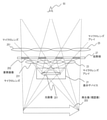
図8は、液晶レンズアレイ80の構成例を示す分解斜視図である。液晶レンズアレイ80は、前側の第1基板81と後側の第2基板82とを含む。第1基板81と第2基板82とは、絶縁性の透明基板である。対向する第1基板81と第2基板82との間に、液晶材料(不図示)が封入される。
[Display device configuration]
FIG. 8 is an exploded perspective view showing a configuration example of the liquid
第1基板81と第2基板82の互いに対向する面に、それぞれ、複数の電極が配置されている。第1基板81の液晶材料に対向する面には、帯状の複数の電極811が配列されている。第2基板82の液晶材料に対向する面には、帯状の複数の電極821が配列されている。電極811、821は、透明導電材料、例えば、ITO(Indium Tin Oxide)やZnO(酸化亜鉛)で形成されている。
A plurality of electrodes are arranged on the surfaces of the first substrate 81 and the second substrate 82 facing each other. A plurality of strip-shaped
帯状の複数の電極811は、同一方向に延びており、その方向と垂直な方向に配列されている。帯状の複数の電極821は、同一方向に延びており、その方向と垂直な方向に配列されている。電極811と電極821とが、基板主面の法線方向において見て(平面視において)、交差するように、第1基板81及び第2基板82は配置、固定される。以下に説明する例において、電極811が延びる方向と電極821が延びる方向との間の角度は、平面視において、直角である。
The band-shaped plurality of
図9Aは、電極811及び電極821のレイアウト及び電極それぞれに与えられる電圧を示す平面図である。図9Aにおいて、電極EL1、EL2、EL3は、第1基板81上に配置されている電極811である。電極EL4、EL5、EL6は、第2基板82上に配置されている電極821である。不図示の駆動回路が、電極811及び電極821それぞれを駆動し、各電極の電位を制御する。
FIG. 9A is a plan view showing the layout of the
配列された電極811は、ストライプパターンを有する。電極811は、図9Aにおいて左右方向に延び、上下方向に配列されている。電極811の形状は同一であり、上下方向において等間隔で配列されている。配列された電極821は、ストライプパターンを有する。電極821は、図9Aにおい上下方向に延び、左右方向に配列されている。電極821の形状は同一であり、左右方向において等間隔で配列されている。
The arranged
電極811と電極821とは、平面視において交差しており、図9Aの例において、電極811と電極821とは直交している。電極811と電極821は同一の形状を有し、配列ピッチも同一である。電極811と電極821の形状及び/又はピッチは異なっていてもよい。電極811と電極821とは直交していなくてもよい。
The
第1基板81の電極811のうち、X[mm]間隔の電極EL1、EL2、EL3は、接地され、0[V]が与えられている。電極811の他の電極は、フローティング状態である。第2基板82の電極821のうち、X[mm]間隔の電極EL4、EL5、EL6に対して、正の電圧V1[V]が与えられている。電極821の他の電極は、フローティング状態である。
Of the
図9Bは、図9AにおけるBB切断線での断面における、電位分布及び屈折率分布を示す。図9Cは、図9AにおけるCC切断線での断面における、電位分布及び屈折率分布を示す。図9Bに示すように、屈折率は、電極EL4、EL5、EL6の位置で最も小さく、電極EL4、EL5間の中央位置、及び、電極EL5、EL6間の中央位置に向かって漸増し、それら中央位置で最も高くなっている。 FIG. 9B shows the potential distribution and the refractive index distribution in the cross section at the BB cutting line in FIG. 9A. FIG. 9C shows the potential distribution and the refractive index distribution in the cross section at the CC cutting line in FIG. 9A. As shown in FIG. 9B, the refractive index is the smallest at the positions of the electrodes EL4, EL5, and EL6, and gradually increases toward the central position between the electrodes EL4 and EL5 and the central position between the electrodes EL5 and EL6, and the center thereof. It is the highest in the position.
また、図9Cに示すように、屈折率は、電極EL1、EL2、EL3の位置で最も小さく、電極EL1、EL2間の中央位置、及び、電極EL2、EL3間の中央位置に向かって漸増し、それら中央位置で最も高くなっている。 Further, as shown in FIG. 9C, the refractive index is the smallest at the positions of the electrodes EL1, EL2 and EL3, and gradually increases toward the central position between the electrodes EL1 and EL2 and the central position between the electrodes EL2 and EL3. It is the highest in their central position.
このように、0[V]が与えられている二つの隣接電極と、V1[V]が与えられている二つの隣接電極とで画定される範囲において、液晶材料が略円形の凸レンズとして透過光に作用する。つまり、直径及びピッチがX[mm]の屈折率分布型レンズアレイが形成される。 As described above, in the range defined by the two adjacent electrodes to which 0 [V] is given and the two adjacent electrodes to which V1 [V] is given, the liquid crystal material is transmitted light as a substantially circular convex lens. Acts on. That is, a refractive index distribution type lens array having a diameter and pitch of X [mm] is formed.
具体的には、電極EL1、EL2、EL4、EL5で囲まれる領域、及び、電極EL1、EL2、EL5、EL6で囲まれる領域、それぞれに、屈折率分布型レンズが形成される。また、電極EL2、EL3、EL4、EL5で囲まれる領域、及び、電極EL2、EL3、EL5、EL6で囲まれる領域、それぞれに、屈折率分布型レンズが形成される。 Specifically, a refractive index distribution type lens is formed in each of the region surrounded by the electrodes EL1, EL2, EL4, and EL5 and the region surrounded by the electrodes EL1, EL2, EL5, and EL6. Further, a refractive index distribution type lens is formed in each of the region surrounded by the electrodes EL2, EL3, EL4, and EL5 and the region surrounded by the electrodes EL2, EL3, EL5, and EL6.
0[V]を与える電極の間隔及びV1[V]を与える電極の間隔を増減することで、レンズピッチを増減することができる。なお、第1基板81の電極811にV1[V]を与え、第2基板の電極821に0[V]を与えてもよい。図9B、9Cに示すような電位分布を形成できれば、一方の基板の電極に与える電位は0[V]と異なる電圧V1より低い所定電圧でもよく、二つの基板に与える電位の極性も任意である。電圧V1は、負の電圧であってもよい。
The lens pitch can be increased or decreased by increasing or decreasing the distance between the electrodes that give 0 [V] and the distance between the electrodes that give V1 [V]. It should be noted that V1 [V] may be given to the
図10は、第2マイクロレンズアレイに、液晶レンズアレイ80を使用した表示装置20の構成例を示す。液晶レンズアレイ80に対して、実施形態1における第2マイクロレンズアレイ25の説明を適用することができる。液晶レンズアレイ80は、上述のように駆動され、レンズピッチX[mm]は、要素画像202の画像ピッチよりも小さい。
FIG. 10 shows a configuration example of a
レンズピッチを変更することで、再生像203の表示位置を変更することができる。例えば、帯状の電極811、821の幅が0.02[mm]、電極間ピッチが0.04[mm]とする。拡散板27に映された要素画像202のピッチが1[mm]とする。液晶レンズアレイ80が、レンズピッチX=0.96[mm]で駆動されると、再生像203は、拡散板27の前側で視認される。液晶レンズアレイ80が、レンズピッチX=1.04[mm]で駆動されると、再生像203は拡散板27の後側に視認される。
By changing the lens pitch, the display position of the reproduced
次に、液晶レンズアレイ80の他の駆動例を説明する。図11Aは、電極811及び電極821のレイアウト及び電極それぞれに与えられる電圧を示す平面図である。第1基板81の電極811のうち、X[mm]間隔の電極EL1、EL2、EL3は、接地され、0[V]が与えられている。電極811のうち、他の電極はフローティング状態である。
Next, another driving example of the liquid
第2基板82の電極821のうち、X[mm]間隔の電極EL4、EL5、EL6に対して、正の電圧V1[V]が与えられている。さらに、第2基板82の電極821のうち、電圧V1[V]が与えられている電極間の中央に位置する電極EL7、EL8が接地され、0[V]が与えられている。電極821のうち、他の電極はフローティング状態である。図9A、9B、9Cを参照して説明した駆動方法と比較して、電極EL7、EL8の電圧が異なる。他の点は、上記駆動方法と同様である。
A positive voltage V1 [V] is applied to the electrodes EL4, EL5, and EL6 at intervals of X [mm] among the
図11Bは、図11AにおけるBB切断線での断面における、電位分布及び屈折率分布を示す。また、図9Cを参照した説明が、本駆動方法にも適用できる。上記駆動方法と同様に、液晶レンズアレイ80は、直径及びピッチがX[mm]の屈折率分布型レンズアレイとして作用する。さらに、電極EL7とEL8に0[V]を与えることで、低電位のピーク位置を正確に定めることができ、上記駆動方法と比較し、レンズの光軸位置をより正確に定めることができる。電極EL1、EL2、EL3、EL7、EL8に与える電圧は、0[V]と異なる電圧V1[V]より低い所定電圧でもよい。
FIG. 11B shows the potential distribution and the refractive index distribution in the cross section at the BB cut line in FIG. 11A. Further, the description with reference to FIG. 9C can be applied to this driving method. Similar to the above driving method, the liquid
次に、液晶レンズアレイ80の他の構成例を説明する。図12は、液晶レンズアレイ80の他の構成例の分解斜視図である。液晶レンズアレイ80は、前側の第1液晶セル850と、後側の第2液晶セル860とを含む。
Next, another configuration example of the liquid
第1液晶セル850は、第1基板851と第2基板852とを含む。第1基板851と第2基板852とは、絶縁性の透明基板である。対向する第1基板851と第2基板852との間に、液晶材料(不図示)が封入される。第1基板851の第2基板852及び液晶材料に対向する面に、面状の電極853が配置されている。第2基板852の第1基板851及び液晶材料に対向する面に、ストライプパターンの複数の電極854が配置されている。
The first
第2基板852上で、帯状の複数の電極854が同一方向に延びており、その方向と垂直な方向に配列されている。面状の電極853と全ての複数の電極854とが、対向している。電極853、854は、透明導電材料、例えば、ITO(Indium Tin Oxide)やZnO(酸化亜鉛)で形成されている。
On the
第2液晶セル860は、第1基板861と第2基板862とを含む。第1基板861と第2基板862とは、絶縁性の透明基板である。対向する第1基板861と第2基板862との間に、液晶材料(不図示)が封入される。第1基板861の第2基板862及び液晶材料に対向する面に、面状の電極863が配置されている。第2基板862の第1基板861及び液晶材料に対向する面に、ストライプパターンの複数の電極864が配置されている。
The second
第2基板862上で、帯状の複数の電極864が同一方向に延びており、その方向と垂直な方向に配列されている。面状の電極863と全ての複数の電極864とが、対向している。電極863、864は、透明導電材料、例えば、ITO(Indium Tin Oxide)やZnO(酸化亜鉛)で形成されている。
On the
第1液晶セル850のストライプパターンを有する電極854と、第2液晶セル860のストライプパターンを有する電極864とが、直行するように、第1液晶セル850及び第2液晶セル860は積層され、固定される。
The first
図13Aは、第1液晶セル850のストライプパターンの電極854の一部及びそれらに与えられる電圧を示す平面図である。電極854のうち、X[mm]間隔の電極EL1、EL2、EL3に、正電圧V1[V]が与えられている。電圧V1[V]が与えられている電極間の中央に位置する電極EL4、EL5は、接地され、0[V]が与えられている。電極854の他の電極はフローティング状態である。電極854に対向する面状電極853は接地され、0[V]が与えられる。
FIG. 13A is a plan view showing a part of the
図13Bは、図13AにおけるBB切断線での断面における、電位分布及び屈折率分布を示す。屈折率は、電圧V1[V]が与えられている電極EL1、EL2、EL3の位置において最も小さく、電極EL4、EL5位置で最も大きい。屈折率は、電極EL1、EL2、EL3から、電極EL4又はEL5に向かって、漸増している。図13Aの屈折率分布から理解されるように、電圧V1[V]が与えられている隣接電極間の領域は、X[mm]幅の屈折率分布型のシリンドリカルレンズとして作用する。 FIG. 13B shows the potential distribution and the refractive index distribution in the cross section at the BB cut line in FIG. 13A. The refractive index is the smallest at the positions of the electrodes EL1, EL2, and EL3 to which the voltage V1 [V] is applied, and is the largest at the positions of the electrodes EL4 and EL5. The refractive index gradually increases from the electrodes EL1, EL2, and EL3 toward the electrodes EL4 or EL5. As can be understood from the refractive index distribution of FIG. 13A, the region between the adjacent electrodes to which the voltage V1 [V] is applied acts as a refractive index distribution type cylindrical lens having an X [mm] width.
第2液晶セル860も、第1液晶セル850と同様に、上述のように駆動される。第2液晶セル860が形成するX[mm]幅のシリンドリカルレンズは、第1液晶セル850が形成するX[mm]幅のシリンドリカルレンズに、平面視において交差し、本例において、直交する。これらは、直交していなくてもよい。液晶レンズアレイ80は、直径及びピッチがX[mm]の屈折率分布型レンズアレイとして作用する。
The second
なお、上記の屈折率分布を得ることができれば、電極に与える電圧は、上記例に限定されない、例えば、上記駆動における0[V]に代えて、電圧V1より小さい正又は負の所定電圧を与えてもよい。 If the above-mentioned refractive index distribution can be obtained, the voltage applied to the electrodes is not limited to the above-mentioned example. For example, instead of 0 [V] in the above-mentioned drive, a positive or negative predetermined voltage smaller than the voltage V1 is given. You may.
[表示装置の制御]
以下において、液晶レンズアレイ80を含む表示装置20の制御を説明する。図14Aは、表示装置20を含む表示システム1の論理構成を示す。表示システム1は、表示装置20を制御する表示制御部10をさらに含む。表示制御部10は、表示デバイス21を制御する画像制御部11及び液晶レンズアレイ80を制御する液晶レンズ制御部13を含む。本例において、液晶レンズアレイ80は、要素画像202の前側に配置されている。
[Display device control]
Hereinafter, the control of the
画像制御部11は、元画像(データ)53から、表示デバイス21に元画像201を表示させるための制御信号を、表示デバイス21に送信する。表示デバイス21は、元画像201をスクリーン上で表示する。
The
液晶レンズ制御部13は、ユーザ入力51に基づき、液晶レンズアレイ80を制御する。具体的には、液晶レンズ制御部13は、ユーザが指定した再生像203の表示位置を示す情報に基づき、液晶レンズアレイ80のレンズピッチを制御する。再生像203の位置は、例えば、ユーザに最も近い位置から最も遠い位置までのいくつかの位置から選択可能である。指定可能な位置は、例えば、要素画像202の前側及び後側の位置を含む。なお、液晶レンズ制御部13が受け付ける再生像203の位置の指定方法は特に限定されない。
The liquid crystal
液晶レンズ制御部13は、ユーザに指定され得る再生像203の表示位置と、液晶レンズアレイ80の電極それぞれに対して与える電圧とを対応付ける情報を保持している。再生像203の位置は、液晶レンズアレイ80のレンズピッチに対応する。液晶レンズアレイ80のレンズピッチは、上述のように制御することができる。液晶レンズ制御部13は、ユーザ指定された再生像203の位置に対応するレンズピッチとなるように、液晶レンズアレイ80に制御信号を送信する。これにより、ユーザの視力や位置等のユーザ状態に応じて適切な再生像203を形成することができる。
The liquid crystal
図14Bに、表示システム1のハードウェア構成例を模式的に示す。表示システム1は、表示装置20に加え、制御装置102及び入力デバイス127を含む。制御装置102は、例えば、計算機構成を有することができる。具体的には、制御装置102は、例えば、プロセッサ121、入出力インタフェース(I/F)122、通信I/F123、補助記憶装置125、及びメモリ126を含む。これらはバスを介して接続されている。
FIG. 14B schematically shows a hardware configuration example of the
入出力インタフェース122は、複数のポートを含み、複数の外部デバイスと接続され得る。図14Bにおいて、入出力インタフェース122には、表示装置20が接続される。表示デバイス21及び液晶レンズアレイ80への制御信号は、入出力インタフェース122から送信される。
The input /
入出力インタフェース122は、さらに、入力デバイス127に接続されている。入力デバイス127は、ユーザに操作されるデバイスであって、例えば、タッチパネルデバイス(表示デバイスと共に使用される)や操作ボタンである。入力デバイス127からの信号は、入出力インタフェース122により受信される。
The input /
通信インタフェース123は、所定のプロトコルに従って、他の装置との通信を制御するネットワークインタフェース装置である。通信インタフェース123は、外部メモリと接続するためのインタフェースを含んでもよい。
The
補助記憶装置125は、例えば、フラッシュメモリデバイス等の不揮発性記憶装置であり、プロセッサ121が実行するプログラム及びプログラムの実行時に使用されるデータを格納する。本例において、補助記憶装置125は、元画像53を格納している。補助記憶装置125は、複数の元画像を格納し得る。元画像53は静止画像であるが、複数の元画像により、動画像を構成することができる。
The
一般に、補助記憶装置125に格納されているデータは、メモリ126にロードされて使用される。メモリ126は、例えば、揮発性メモリであり、プロセッサ121が実行するプログラム及びプログラムの実行時に使用されるデータを格納する。補助記憶装置125、メモリ126及びこれらの組み合わせは、それぞれ、記憶装置である。
Generally, the data stored in the
プロセッサ121は、メモリ126に格納されたプログラムを実行する。プロセッサ121は、プログラムに従って動作することによって、所定の機能を実現する機能部(手段)として動作する。例えば、プロセッサ121は、画像制御プログラムに従って動作することで画像制御部11として機能し、液晶レンズアレイ制御プログラムに従って動作することで液晶レンズ制御部13として機能する。
The
本例において、画像制御部11及び液晶レンズ制御部13は、プロセッサ121により実装されているが、これらの機能を有する論理回路がプロセッサ121とは別に実装されてもよい。
In this example, the
上述のように、液晶レンズアレイ80は、レンズピッチを変更可能なマイクロレンズアレイとして動作する。液晶レンズアレイが、要素画像202を生成する構成においては、要素画像202のピッチを制御するように、液晶レンズアレイの電極に与える電圧が制御される。要素画像202の生成及び統合のそれぞれに液晶レンズアレイが使用される場合、双方又は一方のみのレンズピッチは、ユーザ指定に応じて制御してよい。
As described above, the liquid
実施形態2において説明したように、ピンホールアレイをマイクロレンズアレイに代えて使用することができ、ピンホールピッチを変更可能なピンホールアレイとして、透過型表示デバイス、例えば、液晶表示デバイスを使用することができる。表示制御部10は、液晶表示デバイスにおいてピンホールアレイの画像を表示する。ピンホールそれぞれの領域は光を透過させ、ピンホール以外の領域は、光を遮断又は散乱する。ピンホールピッチを制御することで、再生像203の位置を制御することができる。
As described in the second embodiment, a transmissive display device, for example, a liquid crystal display device is used as the pinhole array in which the pinhole array can be used instead of the microlens array and the pinhole pitch can be changed. be able to. The
以上、本発明の実施形態を説明したが、本発明が上記の実施形態に限定されるものではない。当業者であれば、上記の実施形態の各要素を、本発明の範囲において容易に変更、追加、変換することが可能である。ある実施形態の構成の一部を他の実施形態の構成に置き換えることが可能であり、ある実施形態の構成に他の実施形態の構成を加えることも可能である。 Although the embodiments of the present invention have been described above, the present invention is not limited to the above embodiments. A person skilled in the art can easily change, add, or convert each element of the above embodiment within the scope of the present invention. It is possible to replace a part of the configuration of one embodiment with the configuration of another embodiment, and it is also possible to add the configuration of another embodiment to the configuration of one embodiment.
1 表示システム、10 表示制御部、11 画像制御部、13 液晶レンズ制御部、20 表示装置、21 表示デバイス、23、25 マイクロレンズアレイ、24、26 ピンホールアレイ、27 拡散板、50 ユーザ、51 ユーザ入力、53 元画像データ、80 液晶レンズアレイ、81、82 基板、102 制御装置、121 プロセッサ、122 入出力インタフェース、123 通信インタフェース、125 補助記憶装置、126 メモリ、127 入力デバイス、201 元画像、202 要素画像、203 再生像、211 プロジェクタ、212 プロジェクションスクリーン、231、251 マイクロレンズ、241、261 ピンホール、811、821 電極、850、860 液晶セル、851、852、861、862 基板、853、854、8653、864 電極、EL1~EL8 電極、P1 レンズピッチ、P2 画像ピッチ 1 Display system, 10 Display control unit, 11 Image control unit, 13 Liquid crystal lens control unit, 20 Display device, 21 Display device, 23, 25 Microlens array, 24, 26 Pinhole array, 27 Diffuse plate, 50 users, 51 User input, 53 original image data, 80 liquid crystal lens array, 81, 82 boards, 102 control device, 121 processor, 122 input / output interface, 123 communication interface, 125 auxiliary storage device, 126 memory, 127 input device, 201 original image, 202 element image, 203 reproduction image, 211 projector, 212 projection screen, 231 and 251 microlens, 241 and 261 pinholes, 811, 821 electrodes, 850 and 860 liquid crystal cells, 851, 852, 861 and 862 substrates, 853 and 854. , 8653, 864 electrodes, EL1 to EL8 electrodes, P1 lens pitch, P2 image pitch
Claims (9)
レンズアレイ又はピンホールアレイである、第2アレイと、
前記表示デバイスと前記第2アレイとの間に、前記表示デバイス及び前記第2アレイから離間して配置された、レンズアレイ又はピンホールアレイである、第1アレイと、
を含み、
前記第1アレイは、前記元画像から生成した複数の要素画像を、前記第1アレイと前記第2アレイとの間に結像し、
前記複数の要素画像のピッチは、前記第2アレイのレンズピッチ又はピンホールピッチと異なり、
前記第2アレイは、前記複数の要素画像を統合して、前記元画像を表す一つの再生像を生成し、
前記第1アレイ及び前記第2アレイの少なくとも一方は、レンズピッチを変更可能なレンズアレイである、
表示装置。 A display device that displays the original image at the original image display position,
A second array, which is a lens array or a pinhole array,
A first array, which is a lens array or a pinhole array, arranged between the display device and the second array so as to be separated from the display device and the second array.
Including
The first array forms a plurality of element images generated from the original image between the first array and the second array.
The pitch of the plurality of element images is different from the lens pitch or pinhole pitch of the second array.
The second array integrates the plurality of element images to generate one reproduced image representing the original image .
At least one of the first array and the second array is a lens array whose lens pitch can be changed.
Display device.
前記第2アレイのレンズピッチ又はピンホールピッチは、前記複数の要素画像のピッチよりも大きく、
前記再生像は、前記複数の要素画像の後側に位置する虚像である、
表示装置。 The display device according to claim 1.
The lens pitch or pinhole pitch of the second array is larger than the pitch of the plurality of element images.
The reproduced image is a virtual image located behind the plurality of element images.
Display device.
前記第2アレイのレンズピッチ又はピンホールピッチは、前記複数の要素画像のピッチよりも小さく、
前記再生像は、前記複数の要素画像の前側に位置する実像である、
表示装置。 The display device according to claim 1.
The lens pitch or pinhole pitch of the second array is smaller than the pitch of the plurality of element images.
The reproduced image is a real image located in front of the plurality of element images.
Display device.
前記第1アレイと前記第2アレイとの間に配置され、前記複数の要素画像における要素画像からの光線の少なくとも一部の方向を、前記再生像の生成に使用するように制御する、光線方向制御板、をさらに含む、
表示装置。 The display device according to claim 1.
A ray direction arranged between the first array and the second array that controls the direction of at least a portion of the rays from the element images in the plurality of element images to be used to generate the reproduced image. Control plate, including,
Display device.
前記複数の要素画像は、前記光線方向制御板内で結像されている、
表示装置。 The display device according to claim 4.
The plurality of element images are imaged in the ray direction control plate.
Display device.
前記光線方向制御板は拡散板である、
表示装置。 The display device according to claim 4.
The ray direction control plate is a diffusion plate.
Display device.
前記レンズアレイは、 The lens array is
対向する第1基板及び第2基板と、 Opposing first and second boards,
前記第1基板と前記第2基板との間の液晶と、 The liquid crystal display between the first substrate and the second substrate,
前記第1基板の前記第2基板に対向する面に形成されたストライプ状の第1電極パターンと、 A striped first electrode pattern formed on the surface of the first substrate facing the second substrate, and
前記第2基板の前記第1基板に対向する面に形成され、前記第1電極パターンと交差する、ストライプ状の第2電極パターンと、 A striped second electrode pattern formed on the surface of the second substrate facing the first substrate and intersecting with the first electrode pattern.
を含み、 Including
前記第1電極パターンにおける所定間隔の電極に対して所定電圧が与えられ、前記第1電極パターンにおける他の電極はフローティング状態であり、 A predetermined voltage is applied to the electrodes at predetermined intervals in the first electrode pattern, and the other electrodes in the first electrode pattern are in a floating state.
前記第2電極パターンにおける所定間隔の電極に対して前記所定電圧より低い電圧が与えられ、前記第2電極パターンにおける他の電極はフローティング状態である、 A voltage lower than the predetermined voltage is applied to the electrodes at predetermined intervals in the second electrode pattern, and the other electrodes in the second electrode pattern are in a floating state.
表示装置。 Display device.
前記第1電極パターンにおいて前記所定電圧が与えられている電極間の中央の電極に、前記所定電圧より低い前記電圧が与えられている、 The voltage lower than the predetermined voltage is applied to the central electrode between the electrodes to which the predetermined voltage is applied in the first electrode pattern.
表示装置。 Display device.
前記レンズアレイは、 The lens array is
積層配置されている第1液晶セルと第2液晶セルとを含み、 Including the first liquid crystal cell and the second liquid crystal cell which are arranged in a stacked manner,
前記第1液晶セルは、 The first liquid crystal cell is
対向する第1基板及び第2基板と、 Opposing first and second boards,
前記第1基板と前記第2基板との間の液晶と、 The liquid crystal display between the first substrate and the second substrate,
前記第1基板の前記第2基板に対向する面に形成された第1面状電極と、 The first planar electrode formed on the surface of the first substrate facing the second substrate, and
前記第2基板の前記第1基板に対向する面に形成された、ストライプ状の第1電極パターンと、 A striped first electrode pattern formed on the surface of the second substrate facing the first substrate, and
を含み、 Including
前記第2液晶セルは、 The second liquid crystal cell is
対向する第3基板及び第4基板と、 Opposing 3rd and 4th boards,
前記第3基板と前記第4基板との間の液晶と、 The liquid crystal display between the third substrate and the fourth substrate,
前記第3基板の前記第4基板に対向する面に形成された第2面状電極と、 A second planar electrode formed on the surface of the third substrate facing the fourth substrate, and
前記第4基板の前記第3基板に対向する面に形成され、第1電極パターンと交差する、ストライプ状の第2電極パターンと、 A striped second electrode pattern formed on the surface of the fourth substrate facing the third substrate and intersecting with the first electrode pattern.
を含み、 Including
前記第1電極パターンにおける所定間隔の電極に対して第1所定電圧が与えられ、前記第1電極パターンにおける他の電極はフローティング状態であり、 A first predetermined voltage is applied to the electrodes at predetermined intervals in the first electrode pattern, and the other electrodes in the first electrode pattern are in a floating state.
前記第1面状電極に対して前記第1所定電圧より低い電圧が与えられ、 A voltage lower than the first predetermined voltage is applied to the first planar electrode, and a voltage lower than the first predetermined voltage is applied.
前記第2電極パターンにおける所定間隔の電極に対して第2所定電圧が与えられ、前記第2電極パターンにおける他の電極はフローティング状態であり、 A second predetermined voltage is applied to the electrodes at predetermined intervals in the second electrode pattern, and the other electrodes in the second electrode pattern are in a floating state.
前記第2面状電極に対して前記第2所定電圧より低い電圧が与えられる、 A voltage lower than the second predetermined voltage is applied to the second planar electrode.
表示装置。 Display device.
Priority Applications (3)
| Application Number | Priority Date | Filing Date | Title |
|---|---|---|---|
| JP2018015517A JP7011161B2 (en) | 2018-01-31 | 2018-01-31 | Display device |
| CN201910053672.1A CN110095872B (en) | 2018-01-31 | 2019-01-21 | Display device |
| US16/263,038 US10824002B2 (en) | 2018-01-31 | 2019-01-31 | Display apparatus |
Applications Claiming Priority (1)
| Application Number | Priority Date | Filing Date | Title |
|---|---|---|---|
| JP2018015517A JP7011161B2 (en) | 2018-01-31 | 2018-01-31 | Display device |
Publications (3)
| Publication Number | Publication Date |
|---|---|
| JP2019133028A JP2019133028A (en) | 2019-08-08 |
| JP2019133028A5 JP2019133028A5 (en) | 2021-02-18 |
| JP7011161B2 true JP7011161B2 (en) | 2022-02-10 |
Family
ID=67392060
Family Applications (1)
| Application Number | Title | Priority Date | Filing Date |
|---|---|---|---|
| JP2018015517A Active JP7011161B2 (en) | 2018-01-31 | 2018-01-31 | Display device |
Country Status (3)
| Country | Link |
|---|---|
| US (1) | US10824002B2 (en) |
| JP (1) | JP7011161B2 (en) |
| CN (1) | CN110095872B (en) |
Families Citing this family (4)
| Publication number | Priority date | Publication date | Assignee | Title |
|---|---|---|---|---|
| WO2020143915A1 (en) * | 2019-01-10 | 2020-07-16 | Osram Gmbh | Image displaying device and method for displaying an image on a screen |
| EP4001242A4 (en) | 2019-07-18 | 2022-08-31 | Sumitomo Electric Industries, Ltd. | Cubic boron nitride sintered body |
| EP3855219A1 (en) * | 2020-01-21 | 2021-07-28 | Focuslight Technologies Inc. | Diffuser device |
| CN111323978B (en) * | 2020-04-08 | 2021-03-16 | Tcl华星光电技术有限公司 | Pixel unit, array substrate and display panel |
Citations (7)
| Publication number | Priority date | Publication date | Assignee | Title |
|---|---|---|---|---|
| JP2003195215A (en) | 2001-12-28 | 2003-07-09 | Toshiba Corp | Three-dimensional display device |
| JP2006259058A (en) | 2005-03-16 | 2006-09-28 | Matsushita Electric Ind Co Ltd | Three-dimensional picture display device |
| JP2007233253A (en) | 2006-03-03 | 2007-09-13 | Nippon Hoso Kyokai <Nhk> | Stereoscopic video display device |
| JP2011008167A (en) | 2009-06-29 | 2011-01-13 | Nippon Hoso Kyokai <Nhk> | Stereoscopic image display |
| JP2012098689A (en) | 2010-11-04 | 2012-05-24 | Samsung Mobile Display Co Ltd | Optical unit and display device including the same |
| JP2014032281A (en) | 2012-08-02 | 2014-02-20 | Nippon Hoso Kyokai <Nhk> | Reproduced image display device |
| JP2017003981A (en) | 2015-06-12 | 2017-01-05 | 群創光電股▲ふん▼有限公司 | Display device and method for operating display device |
Family Cites Families (18)
| Publication number | Priority date | Publication date | Assignee | Title |
|---|---|---|---|---|
| JPS56158320A (en) * | 1980-05-12 | 1981-12-07 | Victor Co Of Japan Ltd | 3-dimensional display device |
| US4878735A (en) * | 1988-01-15 | 1989-11-07 | Lookingglass Technology, Inc. | Optical imaging system using lenticular tone-plate elements |
| EP0451681B1 (en) * | 1990-04-05 | 1997-11-05 | Seiko Epson Corporation | Optical apparatus |
| JPH0833591B2 (en) * | 1990-08-27 | 1996-03-29 | 日本ビクター株式会社 | 3D display device |
| US5499138A (en) * | 1992-05-26 | 1996-03-12 | Olympus Optical Co., Ltd. | Image display apparatus |
| JP2862462B2 (en) * | 1993-09-09 | 1999-03-03 | シャープ株式会社 | 3D display device |
| JP3980242B2 (en) * | 2000-03-10 | 2007-09-26 | パイオニア株式会社 | Stereoscopic two-dimensional image display apparatus and image display method |
| KR100433276B1 (en) * | 2001-05-02 | 2004-05-31 | 대한민국 | Three-dimensional display |
| JP4202676B2 (en) * | 2002-05-08 | 2008-12-24 | パイオニア株式会社 | Image display device and information recording medium |
| JP2010169847A (en) * | 2009-01-22 | 2010-08-05 | Sony Corp | Spatial image display |
| JP2010224191A (en) * | 2009-03-23 | 2010-10-07 | Toshiba Corp | Apparatus for displaying stereoscopic image |
| JP2011095369A (en) * | 2009-10-28 | 2011-05-12 | Sony Corp | Stereoscopic image display device and method of driving the same |
| JP5657508B2 (en) * | 2011-12-13 | 2015-01-21 | 株式会社ジャパンディスプレイ | Liquid crystal display device, electronic device, and optical device |
| CN103207511B (en) * | 2012-01-11 | 2016-01-13 | 台达电子工业股份有限公司 | Multi-view stereoscopic display |
| CN202948239U (en) * | 2012-12-10 | 2013-05-22 | 京东方科技集团股份有限公司 | Liquid crystal lens and 3D (three-dimensional) display device |
| CN203299500U (en) * | 2013-06-09 | 2013-11-20 | 京东方科技集团股份有限公司 | Double-layer structure liquid crystal lens and 3D display device |
| TW201500805A (en) * | 2013-06-25 | 2015-01-01 | Wintek Corp | Liquid crystal lens, stereoscopic display device and displaying method thereof |
| EP3261083A4 (en) * | 2015-02-18 | 2018-10-03 | Sony Corporation | Optical sheet, display device and electronic apparatus |
-
2018
- 2018-01-31 JP JP2018015517A patent/JP7011161B2/en active Active
-
2019
- 2019-01-21 CN CN201910053672.1A patent/CN110095872B/en active Active
- 2019-01-31 US US16/263,038 patent/US10824002B2/en active Active
Patent Citations (7)
| Publication number | Priority date | Publication date | Assignee | Title |
|---|---|---|---|---|
| JP2003195215A (en) | 2001-12-28 | 2003-07-09 | Toshiba Corp | Three-dimensional display device |
| JP2006259058A (en) | 2005-03-16 | 2006-09-28 | Matsushita Electric Ind Co Ltd | Three-dimensional picture display device |
| JP2007233253A (en) | 2006-03-03 | 2007-09-13 | Nippon Hoso Kyokai <Nhk> | Stereoscopic video display device |
| JP2011008167A (en) | 2009-06-29 | 2011-01-13 | Nippon Hoso Kyokai <Nhk> | Stereoscopic image display |
| JP2012098689A (en) | 2010-11-04 | 2012-05-24 | Samsung Mobile Display Co Ltd | Optical unit and display device including the same |
| JP2014032281A (en) | 2012-08-02 | 2014-02-20 | Nippon Hoso Kyokai <Nhk> | Reproduced image display device |
| JP2017003981A (en) | 2015-06-12 | 2017-01-05 | 群創光電股▲ふん▼有限公司 | Display device and method for operating display device |
Also Published As
| Publication number | Publication date |
|---|---|
| CN110095872B (en) | 2022-04-12 |
| CN110095872A (en) | 2019-08-06 |
| JP2019133028A (en) | 2019-08-08 |
| US20190235313A1 (en) | 2019-08-01 |
| US10824002B2 (en) | 2020-11-03 |
Similar Documents
| Publication | Publication Date | Title |
|---|---|---|
| JP7011161B2 (en) | Display device | |
| CN101331776B (en) | Display device | |
| US7630131B2 (en) | Image display apparatus and optical member therefor | |
| EP3240037B1 (en) | Display for personal immersion apparatus | |
| JP5454661B2 (en) | Image display device | |
| US8373630B2 (en) | Display device | |
| EP2662725B1 (en) | Lenticular lens, liquid crystal lens, and display component | |
| RU2638084C2 (en) | Autostereoscopic display device | |
| EP3671318B1 (en) | Near-eye display device | |
| JP2005078091A (en) | Multiple-view directional display | |
| KR20110014311A (en) | Liquid crystal lens panel, method of manufacturing the same and display device having the liquid crystal lens panel | |
| JP2010503009A (en) | Autostereoscopic display device | |
| KR20100033193A (en) | Display device | |
| JP2009510538A (en) | Improving lenticular design by providing light blocking features | |
| US20210088808A1 (en) | Multi-view display device | |
| JP4503619B2 (en) | Portable device | |
| US20180275417A1 (en) | Display device | |
| KR20220017017A (en) | Display device and manufacturing method thereof | |
| JP2021056523A (en) | Optical element and optical device | |
| KR20170025745A (en) | Stereoscopic Image Display Device | |
| JP5318014B2 (en) | 3D display device | |
| CN215264304U (en) | Display device and terminal equipment | |
| WO2021166833A1 (en) | Display apparatus and display method | |
| CN117518519B (en) | Three-dimensional display device with arc view points distributed | |
| EP4239377A1 (en) | Lens array and display device including the same |
Legal Events
| Date | Code | Title | Description |
|---|---|---|---|
| A521 | Request for written amendment filed |
Free format text: JAPANESE INTERMEDIATE CODE: A523 Effective date: 20210105 |
|
| A621 | Written request for application examination |
Free format text: JAPANESE INTERMEDIATE CODE: A621 Effective date: 20210105 |
|
| A977 | Report on retrieval |
Free format text: JAPANESE INTERMEDIATE CODE: A971007 Effective date: 20210915 |
|
| A131 | Notification of reasons for refusal |
Free format text: JAPANESE INTERMEDIATE CODE: A131 Effective date: 20211005 |
|
| A521 | Request for written amendment filed |
Free format text: JAPANESE INTERMEDIATE CODE: A523 Effective date: 20211129 |
|
| TRDD | Decision of grant or rejection written | ||
| A01 | Written decision to grant a patent or to grant a registration (utility model) |
Free format text: JAPANESE INTERMEDIATE CODE: A01 Effective date: 20211214 |
|
| A61 | First payment of annual fees (during grant procedure) |
Free format text: JAPANESE INTERMEDIATE CODE: A61 Effective date: 20211227 |
|
| R150 | Certificate of patent or registration of utility model |
Ref document number: 7011161 Country of ref document: JP Free format text: JAPANESE INTERMEDIATE CODE: R150 |