CN110095872B - Display device - Google Patents
Display device Download PDFInfo
- Publication number
- CN110095872B CN110095872B CN201910053672.1A CN201910053672A CN110095872B CN 110095872 B CN110095872 B CN 110095872B CN 201910053672 A CN201910053672 A CN 201910053672A CN 110095872 B CN110095872 B CN 110095872B
- Authority
- CN
- China
- Prior art keywords
- array
- substrate
- display device
- image
- pitch
- Prior art date
- Legal status (The legal status is an assumption and is not a legal conclusion. Google has not performed a legal analysis and makes no representation as to the accuracy of the status listed.)
- Active
Links
Images


Classifications
-
- G—PHYSICS
- G02—OPTICS
- G02B—OPTICAL ELEMENTS, SYSTEMS OR APPARATUS
- G02B3/00—Simple or compound lenses
- G02B3/0006—Arrays
-
- G—PHYSICS
- G02—OPTICS
- G02F—OPTICAL DEVICES OR ARRANGEMENTS FOR THE CONTROL OF LIGHT BY MODIFICATION OF THE OPTICAL PROPERTIES OF THE MEDIA OF THE ELEMENTS INVOLVED THEREIN; NON-LINEAR OPTICS; FREQUENCY-CHANGING OF LIGHT; OPTICAL LOGIC ELEMENTS; OPTICAL ANALOGUE/DIGITAL CONVERTERS
- G02F1/00—Devices or arrangements for the control of the intensity, colour, phase, polarisation or direction of light arriving from an independent light source, e.g. switching, gating or modulating; Non-linear optics
- G02F1/01—Devices or arrangements for the control of the intensity, colour, phase, polarisation or direction of light arriving from an independent light source, e.g. switching, gating or modulating; Non-linear optics for the control of the intensity, phase, polarisation or colour
- G02F1/13—Devices or arrangements for the control of the intensity, colour, phase, polarisation or direction of light arriving from an independent light source, e.g. switching, gating or modulating; Non-linear optics for the control of the intensity, phase, polarisation or colour based on liquid crystals, e.g. single liquid crystal display cells
- G02F1/133—Constructional arrangements; Operation of liquid crystal cells; Circuit arrangements
- G02F1/1333—Constructional arrangements; Manufacturing methods
- G02F1/1335—Structural association of cells with optical devices, e.g. polarisers or reflectors
- G02F1/133526—Lenses, e.g. microlenses or Fresnel lenses
-
- G—PHYSICS
- G02—OPTICS
- G02B—OPTICAL ELEMENTS, SYSTEMS OR APPARATUS
- G02B27/00—Optical systems or apparatus not provided for by any of the groups G02B1/00 - G02B26/00, G02B30/00
- G02B27/09—Beam shaping, e.g. changing the cross-sectional area, not otherwise provided for
- G02B27/0938—Using specific optical elements
- G02B27/095—Refractive optical elements
- G02B27/0955—Lenses
- G02B27/0961—Lens arrays
-
- G—PHYSICS
- G02—OPTICS
- G02B—OPTICAL ELEMENTS, SYSTEMS OR APPARATUS
- G02B30/00—Optical systems or apparatus for producing three-dimensional [3D] effects, e.g. stereoscopic images
- G02B30/20—Optical systems or apparatus for producing three-dimensional [3D] effects, e.g. stereoscopic images by providing first and second parallax images to an observer's left and right eyes
- G02B30/26—Optical systems or apparatus for producing three-dimensional [3D] effects, e.g. stereoscopic images by providing first and second parallax images to an observer's left and right eyes of the autostereoscopic type
- G02B30/27—Optical systems or apparatus for producing three-dimensional [3D] effects, e.g. stereoscopic images by providing first and second parallax images to an observer's left and right eyes of the autostereoscopic type involving lenticular arrays
-
- G—PHYSICS
- G02—OPTICS
- G02B—OPTICAL ELEMENTS, SYSTEMS OR APPARATUS
- G02B30/00—Optical systems or apparatus for producing three-dimensional [3D] effects, e.g. stereoscopic images
- G02B30/50—Optical systems or apparatus for producing three-dimensional [3D] effects, e.g. stereoscopic images the image being built up from image elements distributed over a 3D volume, e.g. voxels
- G02B30/56—Optical systems or apparatus for producing three-dimensional [3D] effects, e.g. stereoscopic images the image being built up from image elements distributed over a 3D volume, e.g. voxels by projecting aerial or floating images
-
- G—PHYSICS
- G02—OPTICS
- G02B—OPTICAL ELEMENTS, SYSTEMS OR APPARATUS
- G02B5/00—Optical elements other than lenses
- G02B5/02—Diffusing elements; Afocal elements
-
- G—PHYSICS
- G02—OPTICS
- G02F—OPTICAL DEVICES OR ARRANGEMENTS FOR THE CONTROL OF LIGHT BY MODIFICATION OF THE OPTICAL PROPERTIES OF THE MEDIA OF THE ELEMENTS INVOLVED THEREIN; NON-LINEAR OPTICS; FREQUENCY-CHANGING OF LIGHT; OPTICAL LOGIC ELEMENTS; OPTICAL ANALOGUE/DIGITAL CONVERTERS
- G02F1/00—Devices or arrangements for the control of the intensity, colour, phase, polarisation or direction of light arriving from an independent light source, e.g. switching, gating or modulating; Non-linear optics
- G02F1/01—Devices or arrangements for the control of the intensity, colour, phase, polarisation or direction of light arriving from an independent light source, e.g. switching, gating or modulating; Non-linear optics for the control of the intensity, phase, polarisation or colour
- G02F1/13—Devices or arrangements for the control of the intensity, colour, phase, polarisation or direction of light arriving from an independent light source, e.g. switching, gating or modulating; Non-linear optics for the control of the intensity, phase, polarisation or colour based on liquid crystals, e.g. single liquid crystal display cells
- G02F1/133—Constructional arrangements; Operation of liquid crystal cells; Circuit arrangements
- G02F1/1333—Constructional arrangements; Manufacturing methods
- G02F1/1335—Structural association of cells with optical devices, e.g. polarisers or reflectors
- G02F1/133504—Diffusing, scattering, diffracting elements
-
- G—PHYSICS
- G02—OPTICS
- G02F—OPTICAL DEVICES OR ARRANGEMENTS FOR THE CONTROL OF LIGHT BY MODIFICATION OF THE OPTICAL PROPERTIES OF THE MEDIA OF THE ELEMENTS INVOLVED THEREIN; NON-LINEAR OPTICS; FREQUENCY-CHANGING OF LIGHT; OPTICAL LOGIC ELEMENTS; OPTICAL ANALOGUE/DIGITAL CONVERTERS
- G02F1/00—Devices or arrangements for the control of the intensity, colour, phase, polarisation or direction of light arriving from an independent light source, e.g. switching, gating or modulating; Non-linear optics
- G02F1/01—Devices or arrangements for the control of the intensity, colour, phase, polarisation or direction of light arriving from an independent light source, e.g. switching, gating or modulating; Non-linear optics for the control of the intensity, phase, polarisation or colour
- G02F1/13—Devices or arrangements for the control of the intensity, colour, phase, polarisation or direction of light arriving from an independent light source, e.g. switching, gating or modulating; Non-linear optics for the control of the intensity, phase, polarisation or colour based on liquid crystals, e.g. single liquid crystal display cells
- G02F1/133—Constructional arrangements; Operation of liquid crystal cells; Circuit arrangements
- G02F1/1333—Constructional arrangements; Manufacturing methods
- G02F1/1343—Electrodes
-
- G—PHYSICS
- G02—OPTICS
- G02F—OPTICAL DEVICES OR ARRANGEMENTS FOR THE CONTROL OF LIGHT BY MODIFICATION OF THE OPTICAL PROPERTIES OF THE MEDIA OF THE ELEMENTS INVOLVED THEREIN; NON-LINEAR OPTICS; FREQUENCY-CHANGING OF LIGHT; OPTICAL LOGIC ELEMENTS; OPTICAL ANALOGUE/DIGITAL CONVERTERS
- G02F1/00—Devices or arrangements for the control of the intensity, colour, phase, polarisation or direction of light arriving from an independent light source, e.g. switching, gating or modulating; Non-linear optics
- G02F1/29—Devices or arrangements for the control of the intensity, colour, phase, polarisation or direction of light arriving from an independent light source, e.g. switching, gating or modulating; Non-linear optics for the control of the position or the direction of light beams, i.e. deflection
- G02F1/294—Variable focal length devices
Abstract
A display device, comprising: a display device configured to display an original image at an original image display position; a second array of lens arrays or pinhole arrays; and a first array of lens arrays or pinhole arrays disposed between the display device and the second array remote from the display device and the second array. The first array is configured to form a plurality of elemental images generated from the original image at locations between the first array and the second array. The pitch of the plurality of elemental images is different from the lens pitch or the pinhole pitch of the second array. The second array is configured to integrate the plurality of elemental images to generate a single reproduced image of the original image.
Description
Technical Field
The present disclosure relates to a display device.
Background
Image reproduction techniques based on the principle of integral photography (integral photography) known as integral imaging (integral imaging) are known. The integral imaging generates a reproduced image (image to be viewed) from a plurality of element images. A typical display system for integrated imaging displays a plurality of elemental images on a screen. Each element image is a reduced original image. The display system emits light from the plurality of elemental images through microlenses (elemental lenses) associated in one-to-one correspondence with the plurality of elemental images to form a reproduced image at a specific position in the air away from the screen.
Disclosure of Invention
In order to increase the resolution of an image reproduced by the above-described conventional display system, a minute elemental image having a high resolution is required. In other words, a display device having high resolution is required. However, there is a limitation in increasing the resolution of the display device, and thus, there is a limitation in reproducing a high-resolution image.
One aspect of the present disclosure is a display device including: a display device configured to display an original image at an original image display position; a second array of lens arrays or pinhole arrays; and a first array of lens arrays or pinhole arrays disposed between the display device and the second array remote from the display device and the second array. The first array is configured to form a plurality of elemental images generated from the original image at locations between the first array and the second array. The pitch of the plurality of elemental images is different from the lens pitch or the pinhole pitch of the second array. The second array is configured to integrate the plurality of elemental images to generate a single reproduced image of the original image.
One aspect of the present disclosure enables formation of a high-resolution image to be viewed at a position remote from a display device displaying an original image.
It is to be understood that both the foregoing general description and the following detailed description are exemplary and explanatory only and are not restrictive of the disclosure.
Drawings
Fig. 1A is an exploded perspective view schematically showing components included in the display device in embodiment 1;
fig. 1B is a sectional view schematically showing a positional relationship of components of a display device and a relationship of an image generated by the display device in a normal direction of a principal plane of a display apparatus in embodiment 1;
fig. 2A is an exploded perspective view of another configuration example of the display device in embodiment 2;
fig. 2B is a sectional view of another configuration example of the display device in embodiment 2;
fig. 3A is an exploded perspective view of still another configuration example of a display device in embodiment 2;
fig. 3B is a sectional view of still another configuration example of the display device in embodiment 2;
fig. 4A is an exploded perspective view of still another configuration example of a display device in embodiment 2;
fig. 4B is a sectional view of still another configuration example of the display device in embodiment 2;
fig. 5 is a sectional view of still another configuration example of a display device in embodiment 2;
fig. 6A is a sectional view showing an example of a relationship among a microlens pitch of the second microlens array, an image pitch of the element image, and a reproduced image in embodiment 3;
fig. 6B is a sectional view showing another example of the relationship among the microlens pitch of the second microlens array, the image pitch of the elemental image, and the reproduced image in embodiment 3;
fig. 7A is an exploded perspective view of an example of a configuration for reproducing a virtual image behind the display device in embodiment 3;
fig. 7B is a sectional view of a configuration example for reproducing a virtual image behind the display apparatus in embodiment 3;
fig. 8 is an exploded perspective view showing a configuration example of a liquid crystal lens array of embodiment 4;
fig. 9A is a plan view showing the electrode layout of the liquid crystal lens array and voltages to be applied to the electrodes in embodiment 4;
fig. 9B shows the potential distribution and the refractive index distribution in the cross section cut along the line B-B in fig. 9A in example 4;
fig. 9C shows the potential distribution and the refractive index distribution in the cross section cut along the line C-C in fig. 9A in example 4;
fig. 10 shows a configuration example of a display device employing a liquid crystal lens array as a second microlens array in embodiment 4;
fig. 11A is a plan view showing the electrode layout of the liquid crystal lens array and voltages to be applied to the electrodes in embodiment 4;
fig. 11B shows the potential distribution and the refractive index distribution in the cross section cut along the line B-B in fig. 11A in example 4;
fig. 12 is an exploded perspective view of another configuration example of a liquid crystal lens array in embodiment 4;
fig. 13A is a plan view showing a part of electrodes in a stripe pattern in a first liquid crystal cell and a voltage to be applied to the electrodes in embodiment 4;
fig. 13B shows the potential distribution and the refractive index distribution in the cross section cut along the line B-B in fig. 13A in example 4;
fig. 14A shows a logical configuration of a display system including the display device in embodiment 4; and is
Fig. 14B schematically shows an example of the hardware configuration of the display system in embodiment 4.
Detailed Description
Hereinafter, embodiments are explicitly described with reference to the accompanying drawings. Common elements in the figures are denoted by the same reference numerals. Elements in the drawings may be exaggerated in size or shape for clarity of illustration.
Disclosed herein is a display device that displays an image to be viewed reproduced from an original image on a display at a position different from that of the original image. The display apparatus includes a display device for displaying an original image, a first lens array, and a second lens array. The first lens array is arranged between the display device and the second lens array. The first lens array generates a plurality of elemental images from an original image to form an image between the first lens array and the second lens array. The second lens array integrates the plurality of elemental images to form one reproduced image. As a result, the reproduced image is formed at a position different from that of the original image. Since the display device needs to display one original image without displaying a plurality of element images, a high-resolution reproduced image can be generated.
Example 1
Fig. 1A is an exploded perspective view schematically showing components included in the display device 20 in this embodiment. The display apparatus 20 includes a display device 21, a first microlens array 23, a diffusion plate 27, and a second microlens array 25. The user 50 views a reproduced image (image to be viewed) 203 generated by the display device 20. The user 50 views the reproduced image 203 from the front of the display device 20. In other words, the user side is the front of the display device 20, and the opposite side is the rear of the display device 20.
As shown in fig. 1A, the first microlens array 23 is disposed in front of the display device 21, the diffusion plate 27 is disposed in front of the first microlens array 23, and the second microlens array 25 is disposed in front of the diffusion plate 27. A diffusion plate 27 is interposed between the first microlens array 23 and the second microlens array 25.
The display device 21 may be a liquid crystal display device or an Organic Light Emitting Diode (OLED) display device. The display device 21 may be any type of display device. For example, the display device 21 includes: a display panel including a plurality of pixels arranged in a matrix; a driving circuit for driving the pixels of the display panel; and a control circuit for driving the circuit.
Each of the first microlens array 23 and the second microlens array 25 includes a plurality of microlenses (element lenses) arranged in a matrix. The microlenses may be biconvex lenses or plano-convex lenses. The shape of the microlens is optionally designed, which may be rectangular or circular. The microlens arrays 23 and 25 may be made of resin or glass.
The first microlens array 23 is disposed away from the display device 21. The diffusion plate 27 is disposed away from the first microlens array 23 or in contact with the first microlens array 23. The second microlens array 25 is disposed away from the diffusion plate 27 or in contact with the diffusion plate 27. The second microlens array 25 is disposed away from the first microlens array 23.
The distance between the first microlens array 23 and the front of the display device 21 may be several centimeters to several tens of centimeters. The distance between the first microlens array 23 and the second microlens array 25 may be several millimeters to several centimeters.
For example, the first microlens array 23, the second microlens array 25, and the diffusion plate 27 cover the entire display area of the display device 21 when viewed in the normal direction of the front surface of the display device 21. The centers of the display area of the display device 21, the first microlens array 23, and the second microlens array 25 are located in the normal direction.
The display device 21 displays the original image 201 in its display area. The first microlens array 23 generates a plurality of elemental images 202 from the original image 201. The light of the elemental image 202 is diffused by the diffusion plate 27 and enters the second microlens array 25. The second microlens array 25 integrates the plurality of elemental images 202 with the plurality of two-dimensionally arranged microlenses 251 to generate a reproduced image 203. The reproduced image 203 is an enlarged image of the original image 201; in the example of fig. 1A, a reproduced image 203 is generated (viewed) in front of the second microlens array 25.
Fig. 1B is a sectional view schematically showing the positional relationship of the components of the display device 20 and the relationship of an image generated by the display device 20 in the normal direction of the principal plane of the display apparatus 21. In fig. 1B, a dotted line indicates a chief ray starting from two points of the original image 201, passing through the microlenses 231 and 251, and forming the reproduced image 203. In the example of fig. 1B, the microlenses 231 have the same shape, and the microlenses 251 have the same shape. In fig. 1B, only one microlens of the first microlens array 23 is denoted by reference numeral 231, and only one microlens of the second microlens array 25 is denoted by reference numeral 251.
Each microlens 231 of the first microlens array 23 generates one elemental image 202 from the original image 201 displayed on the display device 21. The microlenses 231 collect light from each point of the original image 201 to a corresponding point of the elemental image 202. A plurality of elemental images 202 are generated between the first microlens array 23 and the second microlens array 25 to be two-dimensionally arranged in a plane like the microlens 231.
Each elemental image 202 is a reduced image of the original image 201, and is formed between the first microlens array 23 and the second microlens array 25. In the example of fig. 1B, each elemental image 202 is formed within the diffuser plate 27. This configuration results in a clearer reproduced image 203. The elemental image 202 may be formed outside the diffusion plate 27, for example, in a space between the diffusion plate 27 and the first microlens array 23.
The diffusion plate 27 is a light direction control plate, and when the diffusion plate 27 is not arranged, the reproduced image 203 is generated with at least a part of the light from the elemental image 202 that is not used for the reproduced image. The diffusion plate 27 adds light to be used for generating the reproduced image 203 from the plurality of elemental images 202 to increase the luminance of the reproduced image 203. A different kind of light direction control plate (such as an optical fiber array) other than the diffusion plate 27 may be employed.
As shown in fig. 1B, light from one elemental image 202 to form the reproduced image 203 passes through one microlens 251 associated with the elemental image 202. The diffusion plate 27 causes more light from the elemental image 202 to enter the microlenses 251 for transmitting light for forming the reproduced image 203, thereby increasing the brightness of the reproduced image 203.
Although the diffusion plate 27 may reduce the light for forming the reproduced image 203 that travels from a portion of the elemental image 202 toward the associated microlens 251, the diffusion plate 27 guides more light for forming the reproduced image 203 from the other elemental images 202 to the associated microlens 251. The diffusion plate 27 adds light for forming a reproduced image 203 to the plurality of elemental images 202 as a whole.
The diffusion plate 27 also makes it difficult for the user 50 to view the original image 201 displayed on the display device 21. In the case where the microlens arrays 23 and 25 include transparent flat non-microlens regions between the microlenses, the user 50 can view the original image 201 through these regions. The diffuser plate 27 disturbs the user 50 in viewing the original image 201. The diffusion plate 27 may be omitted.
The second microlens array 25 integrates the elemental images 202 to generate a reproduced image 203. In the example of fig. 1B, the reproduced image 203 is a real image formed in front of the second microlens array 25. Each microlens 251 collects light from each point of the associated elemental image 202 to a corresponding point of the reproduced image 203. The diffuser plate 27 increases the total light traveling from the elemental image 202 to the reproduced image 203 to increase the brightness of the reproduced image 203.
The above-described configuration of the present embodiment generates the reproduced image 203 from the high-resolution original image 201 displayed on the display device 21, and therefore, the high-resolution reproduced image 203 can be generated.
Example 2
Hereinafter, another configuration example of the display device 20 is described. Differences from embodiment 1 are mainly described. Fig. 2A and 2B are an exploded perspective view and a sectional view, respectively, of another configuration example of the display device 20. The display device 20 in this example includes a pinhole array 24 in place of the first microlens array 23 in the configuration example described with reference to fig. 1A and 1B. The pinhole array 24 includes pinholes 241 arranged in a matrix. In fig. 2B, only one of the pinholes is indicated by way of example with reference numeral 241. The positional relationship of the pinhole array 24 and other components is the same as that of the first microlens array 23 and other components.
The pinhole array 24 forms a plurality of elemental images 202 from the original image 201. An elemental image 202 is formed between the pinhole array 24 and the second microlens array 25 by a pinhole 241. In the example of fig. 2B, elemental images 202 are formed within the diffuser plate 27. Unlike the lens that collects light, the pinhole 241 selectively transmits only light within a particular angle (range of angles) from each point of the original image 201 to form the elemental image 202.
Fig. 3A and 3B are an exploded perspective view and a sectional view, respectively, of still another configuration example of the display device 20. The display device 20 in this example includes a pinhole array 26 in place of the second microlens array 25 in the configuration example described with reference to fig. 1A and 1B. The pinhole array 26 includes pinholes 261 arranged in a matrix. In fig. 3B, only one of the pinholes is indicated by way of example with reference numeral 261. The positional relationship of the pinhole array 26 and other components is the same as that of the second microlens array 25 and other components.
The pinhole array 26 integrates the plurality of elemental images 202 to generate a reconstructed image 203 in front of the pinhole array 26. One pinhole 261 transmits only light within a certain angle (angular range) from each point of the associated elemental image 202. A reproduced image 203 of a real image is generated from the elemental image 202 through a plurality of pinholes 261.
Fig. 4A and 4B are an exploded perspective view and a sectional view, respectively, of still another configuration example of the display device 20. The display device 20 in this example includes: a pinhole array 24 that replaces the first microlens array 23 in the configuration example described with reference to fig. 1A and 1B; and a pinhole array 26 which replaces the second microlens array 25 in fig. 1A and 1B. The foregoing description applies to pinhole arrays 24 and 26.
Fig. 5 is a sectional view showing still another configuration example of the display device 20. The display device 21 of this example includes a projector 211 and a projection screen 212. A reproduced image 203 is generated from the original image 201 displayed on the projection screen 212. The description provided with reference to fig. 1A and 1B applies to the rest. As illustrated in this example, the original image 201 may be displayed on a screen of any type of display device.
Example 3
Hereinafter, the relationship between the pitch of the microlenses in the second microlens array, the pitch of the elemental images, and the reproduced image is described. Fig. 6A and 6B are sectional views showing examples of the relationship among the microlens pitch P1 of the second microlens array 25, the image pitch P2 of the element image 202, and the reproduced image 203. The lens pitch P1 and the image pitch P2 are uniform. The lens pitch P1 and the image pitch P2 may vary according to regions.
In fig. 6A, the microlens pitch P1 of the second microlens array 25 is shorter than the image pitch P2 of the elemental image 202. The reproduced image 203 generated under this condition is a real image formed in front of the second microlens array 25. This is because light from the corresponding points of the plurality of elemental images 202 is collected by the microlens array 25. This configuration in which the reproduced image 203 is formed in front of the display device 20 provides an image that is easy to view particularly for a myopic user.
In the configuration of fig. 6A, when the lens pitch P1 increases relative to the image pitch P2, the reproduced image 203 moves forward and is enlarged. In contrast, when the lens pitch P1 is decreased with respect to the image pitch P2, the reproduced image 203 moves and decreases toward the second microlens array 25. The lens pitch P1 may be shorter than the image pitch P2 by a plurality of percents.
In fig. 6B, the microlens pitch P1 of the second microlens array 25 is longer than the image pitch P2 of the elemental image 202. The reproduced image 203 generated under this condition is a virtual image formed behind the elemental image 202. This is because light from the corresponding points of the plurality of elemental images 202 is diffused after passing through the microlens array 25. This configuration of forming the reproduced image 203 behind the display device 21 provides an image that is easy to see particularly for a far-sighted user.
In the configuration of fig. 6B, when the lens pitch P1 increases relative to the image pitch P2, the reproduced image 203 moves forward to be closer to the elemental image 202 and is reduced. In contrast, when the lens pitch P1 is reduced relative to the image pitch P2, the reproduced image 203 moves backward to be distant from the elemental image 202 and is enlarged. The lens pitch P1 may be longer than the image pitch P2 by multiple percents.
As understood from the above, the position and scale of the reproduced image 203 to be viewed (generated) depend on the relationship between the lens pitch P1 of the second microlens array 25 and the image pitch P2 of the element image 202. The image pitch P2 of the elemental image 202 depends on the lens pitch of the first microlens array 23. Accordingly, the position and scale of the reproduced image 203 to be viewed can be changed by changing the lens pitch of the second microlens array 25 and/or the lens pitch of the first microlens array 23.
The image pitch P2 of the elemental image 202 also depends on the distance between the original image 201 and the first microlens array 23 and the focal length of the first microlens array 23. The lens pitch of the first microlens array 23 and the lens pitch of the second microlens array 25 may be the same or different.
A configuration example of reproducing a virtual image behind a display device is described. Differences from embodiment 1 are mainly described. Fig. 7A and 7B are an exploded perspective view and a sectional view, respectively, of a configuration example for reproducing a virtual image behind a display device. The difference from embodiment 1 is the relationship between the length of the lens pitch of the second microlens array 25 and the length of the image pitch of the elemental image 202.
In the configuration of embodiment 1, the lens pitch of the second microlens array 25 is shorter than the image pitch of the elemental image 202. In the configuration example in fig. 7A and 7B, the lens pitch of the second microlens array 25 is longer than the image pitch of the elemental image 202. In a configuration in which the lens pitch of the second microlens array 25 is shorter than the image pitch of the elemental images 202, a reproduced image 203 is formed in front of the second microlens array 25, as described with reference to fig. 6A.
In contrast, in a configuration in which the lens pitch of the second microlens array 25 is longer than the image pitch of the elemental image 202, the reproduced image 203 is formed as a virtual image behind the elemental image 202, as described with reference to fig. 6B.
Example 4
Hereinafter, a configuration using a liquid crystal microlens array as a microlens array is described. When a potential is applied to the liquid crystal layer, liquid crystals therein are aligned. A refractive index distribution is generated according to the orientation of the liquid crystal, thereby providing the liquid crystal layer with the characteristics of a gradient index lens.
A liquid crystal microlens array may be used as the first microlens array 23 and/or the second microlens array 25. Since the liquid crystal microlens array can be electrically controlled at a lens pitch, the display device can easily generate a reproduced image at an appropriate position according to a user.
Arrangement of display device
Fig. 8 is an exploded perspective view showing a configuration example of the liquid crystal lens array 80. The liquid crystal lens array 80 includes a front first substrate 81 and a rear second substrate 82. The first substrate 81 and the second substrate 82 are insulating transparent substrates. A liquid crystal material (not shown) is encapsulated between the first substrate 81 and the second substrate 82 which are opposite to each other.
A plurality of electrodes are provided on the faces of the first substrate 81 and the second substrate 82 which face each other. On a surface of the first substrate 81 facing the liquid crystal material, a plurality of stripe electrodes 811 are disposed. On the surface of the second substrate 82 facing the liquid crystal material, a plurality of stripe-shaped electrodes 821 are provided. The electrodes 811 and 821 are made of a transparent conductive material such as Indium Tin Oxide (ITO) or zinc oxide (ZnO).
The plurality of stripe electrodes 811 are disposed to extend in the same direction and to be distant from each other in a direction perpendicular to the direction. The plurality of stripe electrodes 821 are disposed to extend in the same direction and to be distant from each other in a direction perpendicular to the direction. The first substrate 81 and the second substrate 82 are fixed in the following orientations: the electrode 811 crosses the electrode 812 when viewed in the normal direction of the front surface of the substrate (in plan view). In the example described below, the angle between the direction in which the electrode 811 extends and the direction in which the electrode 812 extends is a right angle in a plan view.
Fig. 9A is a plan view showing the layout of the electrodes 811 and 821 and the voltages to be applied to the electrodes. In fig. 9A, electrodes EL1, EL2, and EL3 are electrodes 811 provided on the first substrate 81. The electrodes EL4, EL5, and EL6 are electrodes 821 provided on the second substrate 82. A driving circuit, not shown, drives the electrodes 811 and 821 to control the potentials of the electrodes.
The electrodes 811 are disposed in a stripe pattern. The electrodes 811 are disposed to extend in the horizontal direction and to be distant from each other in the vertical direction in fig. 9A. The electrodes 811 have the same shape, and they are arranged at equal intervals in the vertical direction. The electrodes 821 are arranged in a striped pattern. The electrodes 821 are provided to extend in the vertical direction and to be distant from each other in the horizontal direction in fig. 9A. The electrodes 821 have the same shape, and they are arranged at equal intervals in the horizontal direction.
In a plan view, the electrode 811 intersects the electrode 821, and in the example of fig. 9A, the electrode 811 is perpendicular to the electrode 821. The electrode 811 has the same shape as the electrode 821, and the array pitch of the electrode 811 is the same as the array pitch of the electrode 821. The shape and/or spacing of electrodes 811 may be different than the shape and/or spacing of electrodes 821. Electrode 811 need not be perpendicular to electrode 821.
The electrodes EL1, EL2, and EL3 at every X mm among the electrodes 811 on the first substrate 81 are grounded and supplied with 0V. The other electrode 811 is in a floating state. The electrodes EL4, EL5, and EL6 at every X mm of the electrodes 821 on the second substrate 82 are supplied with a positive voltage of V1V. The other electrode 821 is in a floating state.
Fig. 9B shows the potential distribution and the refractive index distribution in a cross section cut along line B-B in fig. 9A. Fig. 9C shows the potential distribution and the refractive index distribution in the cross section cut along the line C-C in fig. 9A. As shown in fig. 9B, the refractive index takes the lowest value at the points of the electrodes EL4, EL5, and EL6, gradually increases toward the midpoint between the electrodes EL4 and EL5 and the midpoint between the electrodes EL5 and EL6, and takes the highest value at the midpoint.
As shown in fig. 9C, the refractive index takes the lowest value at the points of the electrodes EL1, EL2, and EL3, gradually increases toward the midpoint between the electrodes EL1 and EL2 and the midpoint between the electrodes EL2 and EL3, and takes the highest value at the midpoint.
The liquid crystal material acts as a substantially circular convex lens on the light passing therethrough in the region defined by the two adjacent electrodes provided with 0V and the two adjacent electrodes provided with V1V. In other words, a gradient index lens array composed of gradient index lenses having a diameter and pitch of X mm is provided.
Specifically, a gradient index lens is formed in each of a region surrounded by the electrodes EL1, EL2, EL4, and EL5 and a region surrounded by the electrodes EL1, EL2, EL5, and EL 6. Further, a gradient index lens is formed in each of a region surrounded by the electrodes EL2, EL3, EL4, and EL5 and a region surrounded by the electrodes EL2, EL3, EL5, and EL 6.
The lens pitch can be increased or decreased by increasing or decreasing the interval between the electrodes to be provided with 0V and the interval between the electrodes to be provided with V1V. Alternatively, the electrode 811 on the first substrate 81 may be provided with V1V and the electrode 821 on the second substrate 82 may be provided with 0V. As long as the potential distribution as shown in fig. 9B and 9C is generated, the potential of the electrode to be applied to one of the substrates may be a predetermined voltage different from 0V but lower than the voltage V1, and the polarity of the potential to be applied to the two substrates may be freely selected. The voltage V1 may be a negative voltage.
Fig. 10 shows a configuration example of the display device 20 in which a liquid crystal lens array 80 is employed as the second microlens array. The description about the second microlens array 25 in embodiment 1 is applied to the liquid crystal lens array 80. The liquid crystal lens array 80 is driven as described above, and the lens pitch of X mm thereof is shorter than the image pitch of the elemental images 202.
The display position of the reproduced image 203 can be changed by changing the lens pitch. For example, assuming that the width of the stripe-shaped electrodes 811 and 821 is 0.02mm, the pitch of the electrodes is 0.04mm, and the pitch of the elemental images 202 projected on the diffusion plate 27 is 1.00 mm. When the liquid crystal lens array 80 is driven to have a lens pitch X of 0.96mm, the reproduced image 203 is viewed in front of the diffusion plate 27. When the liquid crystal lens array 80 is driven to have a lens pitch X of 1.04mm, the reproduced image 203 is viewed behind the diffusion plate 27.
Next, another example of driving the liquid crystal lens array 80 is described. Fig. 11A is a plan view showing the layout of the electrodes 811 and 821 and the voltages to be applied to the electrodes. The electrodes EL1, EL2, and EL3 at every X mm among the electrodes 811 on the first substrate 81 are grounded and supplied with 0V. The other electrode 811 is in a floating state.
The electrodes EL4, EL5, and EL6 at every X mm of the electrodes 821 on the second substrate 82 are supplied with a positive voltage of V1V. The electrodes EL7 and EL8 at the middle between the electrodes provided with V1V among the electrodes 821 on the second substrate 82 are grounded and provided with 0V. The other electrode 821 is in a floating state. Compared with the driving method described with reference to fig. 9A, 9B, and 9C, the voltages of the electrodes EL7 and EL8 are different. The rest is the same as the above-described driving method.
Fig. 11B shows the potential distribution and the refractive index distribution in a cross section cut along line B-B in fig. 11A. The description provided with reference to fig. 9C is applicable to this driving method. Similar to the first driving method, the liquid crystal lens array 80 functions as a gradient index lens array composed of gradient index lenses having a diameter of X mm and a lens pitch. Further, supplying 0V to the electrodes EL7 and EL8 accurately determines the peak point of the low potential, and therefore, the optical axis of the lens can be accurately determined as compared with the first driving method. The voltages applied to the electrodes EL1, EL2, EL3, EL7, and EL8 may be predetermined voltages other than 0V but lower than the voltage V1V.
Next, another configuration example of the liquid crystal lens array 80 is described. Fig. 12 is an exploded perspective view of another configuration example of the liquid crystal lens array 80. The liquid crystal lens array 80 includes a front first liquid crystal cell 850 and a rear second liquid crystal cell 860.
The first liquid crystal cell 850 includes a first substrate 851 and a second substrate 852. The first substrate 851 and the second substrate 852 are insulating transparent substrates. A liquid crystal material (not shown) is encapsulated between the first substrate 851 and the second substrate 852 opposite to each other. A planar electrode 853 is disposed on the face of the first substrate 851 facing the second substrate 852 and the liquid crystal material. A plurality of electrodes 854 in a stripe pattern are disposed on the side of the second substrate 852 facing the first substrate 851 and the liquid crystal material.
The plurality of stripe electrodes 854 are disposed to extend in the same direction and to be distant from each other in a direction perpendicular to the direction on the second substrate 852. All of the plurality of electrodes 854 face the planar electrode 853. The electrodes 853 and 854 are made of a transparent conductive material such as Indium Tin Oxide (ITO) or zinc oxide (ZnO).
The second liquid crystal cell 860 includes a first substrate 861 and a second substrate 862. The first substrate 861 and the second substrate 862 are insulating transparent substrates. A liquid crystal material (not shown) is enclosed between the first substrate 861 and the second substrate 862 opposite to each other. A planar electrode 863 is disposed on a face of the first substrate 861 facing the second substrate 862 and the liquid crystal material. A plurality of electrodes 864 in a stripe pattern are disposed on a face of the second substrate 862 facing the first substrate 861 and the liquid crystal material.
The plurality of stripe electrodes 864 are disposed to extend in the same direction and to be distant from each other in a direction perpendicular to the direction on the second substrate 862. All of the plurality of electrodes 864 face the planar electrode 863. The electrodes 863 and 864 are made of a transparent conductive material such as Indium Tin Oxide (ITO) or zinc oxide (ZnO).
The first liquid crystal cell 850 and the second liquid crystal cell 860 are stacked and fixed in the following orientations: the electrodes 854 in the stripe pattern of the first liquid crystal cell 850 are perpendicular to the electrodes 864 in the stripe pattern of the second liquid crystal cell 860.
Fig. 13A is a plan view showing a part of the electrode 854 in the stripe pattern in the first liquid crystal cell 850 and a voltage to be applied to the electrode. The electrodes EL1, EL2, and EL3 at every X mm of the electrodes 854 are supplied with a positive voltage of V1V. The electrodes EL4 and EL5 at the midpoint between the electrodes supplied with V1V are grounded and supplied with 0V. The other electrode 854 is in a floating state. The planar electrode 853 opposite to the electrode 854 is grounded and supplied with 0V.
Fig. 13B shows the potential distribution and the refractive index distribution in a cross section cut along line B-B in fig. 13A. The refractive index takes the lowest value at the point of the electrodes EL1, EL2, and EL3 provided with V1V, and takes the highest value at the point of the electrodes EL4 and EL 5. The refractive index gradually increases from the point of the electrodes EL1, EL2, and EL3 to the point of the electrodes EL4 and EL 5. As understood from the refractive index profile in fig. 13A, each region between the electrodes provided with V1V adjacent to each other functions as a cylindrical gradient index lens having a width of X mm.
Similarly to the first liquid crystal cell 850, the second liquid crystal cell 860 is driven as described above. In a plan view, the cylindrical lens having a width of X mm provided by the second liquid crystal cell 860 intersects with the cylindrical lens having a width of X mm provided by the first liquid crystal cell 850. In this example, they intersect vertically. These need not be perpendicular to each other. The liquid crystal lens array 80 functions as a gradient index lens array composed of gradient index lenses having a diameter and a pitch of X mm.
The voltage to be applied to the electrodes is not limited to the foregoing examples as long as the above-described refractive index distribution is obtained. For example, instead of 0V in the above-described driving, a predetermined voltage lower than the voltage V1 or a predetermined negative voltage may be applied.
Control of display device
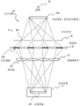
Hereinafter, the control of the display device 20 including the liquid crystal lens array 80 is described. Fig. 14A shows a logical configuration of the display system 1 including the display device 20. The display system 1 further comprises a display controller 10 for controlling the display device 20. The display controller 10 includes an image controller 11 for controlling the display device 21 and a liquid crystal lens controller 13 for controlling the liquid crystal lens array 80. In this example, the liquid crystal lens array 80 is disposed in front of the elemental image 202.
The image controller 11 transmits a control signal for displaying the original image 201 on the display device 21 in accordance with the original image (data) 53. The display device 21 displays the original image 201 on the screen.
The liquid crystal lens controller 13 controls the liquid crystal lens array 80 based on the user input 51. Specifically, the liquid crystal lens controller 13 controls the lens pitch of the liquid crystal lens array 80 according to information on the display position of the reproduced image 203 specified by the user. The position at which the image 203 is reproduced may be selected from a plurality of positions between a position closest to the user and a position farthest from the user. The selection of the location may include a location in front of the elemental image 202 and a location behind the elemental image 202. The manner in which the position of the reproduced image 203 is assigned to the liquid crystal lens controller 13 is not limited to a specific manner.
The liquid crystal lens controller 13 holds information for associating the display position of the reproduced image 203 that can be specified by the user with the voltage to be applied to the electrodes in the liquid crystal lens array 80. The position of the reproduced image 203 depends on the lens pitch of the liquid crystal lens array 80. As described above, the lens pitch of the liquid crystal lens array 80 can be controlled. The liquid crystal lens controller 13 sends a control signal to the liquid crystal lens array 80 to achieve a lens pitch associated with the position of the reproduced image 20 specified by the user. As a result, an appropriate reproduction image 203 is generated according to the conditions of the user (such as visual acuity and the position of the user).
Fig. 14B schematically shows an example of the hardware configuration of the display system 1. In addition to the display apparatus 20, the display system 1 includes a control device 102 and an input device 127. The control device 102 may have a computer configuration. Specifically, the control device 102 includes a processor 121, an input and output interface (input and output I/F)122, a communication interface (communication I/F)123, a secondary storage device 125, and a memory 126. These are connected by a bus.
The input and output interface 122 includes a plurality of ports, and can be connected with a plurality of external devices. In fig. 14B, the input and output interface 122 is connected to the display device 20. Control signals for the display device 21 and the liquid crystal lens array 80 are sent from the input and output interface 122.
The input and output interface 122 is also connected to an input device 127. The input device 127 is a device to be operated by the user, such as a touch panel device (to be used with the display device) or operation buttons. Signals from the input device 127 are received by the input and output interface 122.
The communication interface 123 is a network interface device for controlling communication with other devices according to a predetermined protocol. The communication interface 123 may include an interface for connecting to an external memory.
The secondary storage device 125 is a nonvolatile storage device such as a flash memory device, and stores programs to be executed by the processor 121 and data for executing the programs. The secondary storage device 125 in this example stores the original image 53. The secondary storage device 125 may store a plurality of raw images. Although the original image 53 is a still image, a moving picture can be generated using a plurality of original images.
Typically, data stored in the secondary storage device 125 is loaded into memory 126 for use. The memory 126 may be a volatile memory, and stores programs to be used by the processor 121 and data for executing the programs. Each of the secondary storage device 125, the memory 126, and combinations thereof is a storage device.
The processor 121 executes programs stored in the memory 126. The processor 121 operates according to a program to function as a functional unit (device) that implements a predetermined function. For example, the processor 121 operates according to an image control program to function as the image controller 11 or operates according to a liquid crystal lens control program to function as the liquid crystal lens controller 13.
Although the image controller 11 and the liquid crystal lens controller 13 in this example are implemented by the processor 121, a logic circuit having these functions may be installed in addition to the processor 121.
As described above, the liquid crystal lens array 80 functions as a microlens array whose lens pitch is variable. In the configuration in which the liquid crystal lens array generates the elemental images 202, the voltages to be applied to the electrodes of the liquid crystal lens array are controlled to control the pitches of the elemental images 202. In configurations where an array of liquid crystal lenses is used to generate the elemental image 202 and to integrate the elemental image 202, one or more lens pitches of either or both of the liquid crystal lens arrays may be controlled as specified by a user.
As described in example 2, a pinhole array may replace the microlens array. As the pinhole array whose pinhole pitch is variable, a transmissive display device such as a liquid crystal display device can be employed. The display controller 10 displays an image through a pinhole array on the liquid crystal display device. Each pinhole transmits light, and the area outside the pinhole blocks or diffuses light. The position of the reproduced image 203 can be controlled by controlling the pinhole pitch.
As described above, the embodiments of the present invention have been described; however, the present invention is not limited to the foregoing embodiments. Each element in the foregoing embodiments may be easily modified, added, or converted by those skilled in the art within the scope of the present invention. A part of the configuration of one embodiment may be replaced with the configuration of another embodiment, or the configuration of an embodiment may be incorporated in the configuration of another embodiment.
Claims (8)
1. A display device, comprising:
a display device configured to display an original image at an original image display position;
a second array of lens arrays or pinhole arrays; and
a first array of lens arrays or pinhole arrays disposed between the display device and the second array remote from the display device and the second array,
wherein the first array is configured to form a plurality of elemental images generated from the original image at locations between the first array and the second array,
wherein a pitch of the plurality of elemental images is different from a lens pitch or a pinhole pitch of the second array,
wherein the second array is configured to integrate the plurality of elemental images to generate a single reproduced image of the original image,
wherein the display device further comprises a light direction control panel disposed between the first array and the second array, the light direction control panel being configured to control a direction of at least a portion of light from the plurality of elemental images for use in generating the reproduction image, and
wherein the plurality of elemental images are formed within the light direction control plate.
2. The display device according to claim 1, wherein the first and second light sources are arranged in a matrix,
wherein the second array has a lens pitch or pinhole pitch longer than the pitch of the plurality of elemental images, and
wherein the reproduction image is a virtual image located behind the plurality of elemental images.
3. The display device according to claim 1, wherein the first and second light sources are arranged in a matrix,
wherein the second array has a lens pitch or a pinhole pitch shorter than the pitch of the plurality of elemental images, and
wherein the reproduction image is a real image located in front of the plurality of elemental images.
4. The display device of claim 1, wherein the light direction control plate is a diffuser plate.
5. The display device of claim 1, wherein at least either of the first array and the second array is a variable-pitch lens array.
6. The display device according to claim 5, wherein the first and second light sources are arranged in a matrix,
wherein the lens array with variable lens pitch comprises:
a first substrate and a second substrate opposite to each other;
a liquid crystal between the first substrate and the second substrate;
a striped first electrode pattern formed on a surface of the first substrate facing the second substrate; and
a stripe-shaped second electrode pattern formed on a surface of the second substrate facing the first substrate to cross the first electrode pattern,
wherein electrodes at a predetermined distance in the first electrode pattern are supplied with a predetermined voltage, and the other electrodes in the first electrode pattern are in a floating state, and
wherein the electrodes at a predetermined distance in the second electrode pattern are supplied with a voltage lower than the predetermined voltage, and the other electrodes in the second electrode pattern are in a floating state.
7. The display device according to claim 6, wherein an electrode at a middle between the electrodes in the first electrode pattern to which the predetermined voltage is supplied with the voltage lower than the predetermined voltage.
8. The display device according to claim 5, wherein the first and second light sources are arranged in a matrix,
wherein the lens array with variable lens pitch comprises a first liquid crystal cell and a second liquid crystal cell stacked one on top of the other,
wherein the first liquid crystal cell comprises:
a first substrate and a second substrate opposite to each other;
a liquid crystal between the first substrate and the second substrate;
a first planar electrode formed on a face of the first substrate facing the second substrate; and
a striped first electrode pattern formed on a surface of the second substrate facing the first substrate,
wherein the second liquid crystal cell includes:
a third substrate and a fourth substrate facing each other;
a liquid crystal between the third substrate and the fourth substrate;
a second planar electrode formed on a face of the third substrate facing the fourth substrate; and
a stripe-shaped second electrode pattern formed on a surface of the fourth substrate facing the third substrate to cross the first electrode pattern,
wherein electrodes at a predetermined distance in the first electrode pattern are supplied with a first predetermined voltage, and other electrodes in the first electrode pattern are in a floating state,
wherein the first planar electrode is supplied with a voltage lower than the first predetermined voltage,
wherein electrodes at a predetermined distance in the second electrode pattern are supplied with a second predetermined voltage, and the other electrodes in the second electrode pattern are in a floating state, and
wherein the second planar electrode is supplied with a voltage lower than the second predetermined voltage.
Applications Claiming Priority (2)
| Application Number | Priority Date | Filing Date | Title |
|---|---|---|---|
| JP2018-015517 | 2018-01-31 | ||
| JP2018015517A JP7011161B2 (en) | 2018-01-31 | 2018-01-31 | Display device |
Publications (2)
| Publication Number | Publication Date |
|---|---|
| CN110095872A CN110095872A (en) | 2019-08-06 |
| CN110095872B true CN110095872B (en) | 2022-04-12 |
Family
ID=67392060
Family Applications (1)
| Application Number | Title | Priority Date | Filing Date |
|---|---|---|---|
| CN201910053672.1A Active CN110095872B (en) | 2018-01-31 | 2019-01-21 | Display device |
Country Status (3)
| Country | Link |
|---|---|
| US (1) | US10824002B2 (en) |
| JP (1) | JP7011161B2 (en) |
| CN (1) | CN110095872B (en) |
Families Citing this family (4)
| Publication number | Priority date | Publication date | Assignee | Title |
|---|---|---|---|---|
| DE112019006630T5 (en) * | 2019-01-10 | 2021-09-23 | Osram Gmbh | Image display apparatus and method for displaying an image on a screen |
| US11518718B2 (en) | 2019-07-18 | 2022-12-06 | Sumitomo Electric Industries, Ltd. | Cubic boron nitride sintered material |
| EP3855219A1 (en) * | 2020-01-21 | 2021-07-28 | Focuslight Technologies Inc. | Diffuser device |
| CN111323978B (en) * | 2020-04-08 | 2021-03-16 | Tcl华星光电技术有限公司 | Pixel unit, array substrate and display panel |
Citations (9)
| Publication number | Priority date | Publication date | Assignee | Title |
|---|---|---|---|---|
| US5499138A (en) * | 1992-05-26 | 1996-03-12 | Olympus Optical Co., Ltd. | Image display apparatus |
| KR20020084470A (en) * | 2001-05-02 | 2002-11-09 | 대한민국(서울대학교 총장) | Three-dimensional display |
| JP2007233253A (en) * | 2006-03-03 | 2007-09-13 | Nippon Hoso Kyokai <Nhk> | Stereoscopic video display device |
| JP2010224191A (en) * | 2009-03-23 | 2010-10-07 | Toshiba Corp | Apparatus for displaying stereoscopic image |
| CN102282500A (en) * | 2009-01-22 | 2011-12-14 | 索尼公司 | Spatial image display device |
| CN202948239U (en) * | 2012-12-10 | 2013-05-22 | 京东方科技集团股份有限公司 | Liquid crystal lens and 3D (three-dimensional) display device |
| CN103207511A (en) * | 2012-01-11 | 2013-07-17 | 台达电子工业股份有限公司 | Multi-view stereoscopic display |
| CN203299500U (en) * | 2013-06-09 | 2013-11-20 | 京东方科技集团股份有限公司 | Double-layer structure liquid crystal lens and 3D display device |
| CN104252082A (en) * | 2013-06-25 | 2014-12-31 | 胜华科技股份有限公司 | Liquid crystal lens, stereoscopic display device and display method thereof |
Family Cites Families (16)
| Publication number | Priority date | Publication date | Assignee | Title |
|---|---|---|---|---|
| JPS56158320A (en) * | 1980-05-12 | 1981-12-07 | Victor Co Of Japan Ltd | 3-dimensional display device |
| US4878735A (en) * | 1988-01-15 | 1989-11-07 | Lookingglass Technology, Inc. | Optical imaging system using lenticular tone-plate elements |
| DE69128103T2 (en) * | 1990-04-05 | 1998-04-02 | Seiko Epson Corp | Optical device |
| JPH0833591B2 (en) * | 1990-08-27 | 1996-03-29 | 日本ビクター株式会社 | 3D display device |
| JP2862462B2 (en) * | 1993-09-09 | 1999-03-03 | シャープ株式会社 | 3D display device |
| JP3980242B2 (en) * | 2000-03-10 | 2007-09-26 | パイオニア株式会社 | Stereoscopic two-dimensional image display apparatus and image display method |
| JP3811062B2 (en) * | 2001-12-28 | 2006-08-16 | 株式会社東芝 | 3D image display device |
| JP4202676B2 (en) | 2002-05-08 | 2008-12-24 | パイオニア株式会社 | Image display device and information recording medium |
| JP2006259058A (en) * | 2005-03-16 | 2006-09-28 | Matsushita Electric Ind Co Ltd | Three-dimensional picture display device |
| JP5205339B2 (en) * | 2009-06-29 | 2013-06-05 | 日本放送協会 | 3D image display device |
| JP2011095369A (en) * | 2009-10-28 | 2011-05-12 | Sony Corp | Stereoscopic image display device and method of driving the same |
| KR101729682B1 (en) * | 2010-11-04 | 2017-04-25 | 삼성디스플레이 주식회사 | Optical unit and display device having the same |
| JP5657508B2 (en) * | 2011-12-13 | 2015-01-21 | 株式会社ジャパンディスプレイ | Liquid crystal display device, electronic device, and optical device |
| JP6080121B2 (en) * | 2012-08-02 | 2017-02-15 | 日本放送協会 | Reproduced image display device |
| WO2016132643A1 (en) * | 2015-02-18 | 2016-08-25 | ソニー株式会社 | Optical sheet, display device and electronic apparatus |
| US9881529B2 (en) * | 2015-06-12 | 2018-01-30 | Innolux Corporation | Display device and operating method thereof |
-
2018
- 2018-01-31 JP JP2018015517A patent/JP7011161B2/en active Active
-
2019
- 2019-01-21 CN CN201910053672.1A patent/CN110095872B/en active Active
- 2019-01-31 US US16/263,038 patent/US10824002B2/en active Active
Patent Citations (9)
| Publication number | Priority date | Publication date | Assignee | Title |
|---|---|---|---|---|
| US5499138A (en) * | 1992-05-26 | 1996-03-12 | Olympus Optical Co., Ltd. | Image display apparatus |
| KR20020084470A (en) * | 2001-05-02 | 2002-11-09 | 대한민국(서울대학교 총장) | Three-dimensional display |
| JP2007233253A (en) * | 2006-03-03 | 2007-09-13 | Nippon Hoso Kyokai <Nhk> | Stereoscopic video display device |
| CN102282500A (en) * | 2009-01-22 | 2011-12-14 | 索尼公司 | Spatial image display device |
| JP2010224191A (en) * | 2009-03-23 | 2010-10-07 | Toshiba Corp | Apparatus for displaying stereoscopic image |
| CN103207511A (en) * | 2012-01-11 | 2013-07-17 | 台达电子工业股份有限公司 | Multi-view stereoscopic display |
| CN202948239U (en) * | 2012-12-10 | 2013-05-22 | 京东方科技集团股份有限公司 | Liquid crystal lens and 3D (three-dimensional) display device |
| CN203299500U (en) * | 2013-06-09 | 2013-11-20 | 京东方科技集团股份有限公司 | Double-layer structure liquid crystal lens and 3D display device |
| CN104252082A (en) * | 2013-06-25 | 2014-12-31 | 胜华科技股份有限公司 | Liquid crystal lens, stereoscopic display device and display method thereof |
Also Published As
| Publication number | Publication date |
|---|---|
| JP2019133028A (en) | 2019-08-08 |
| US10824002B2 (en) | 2020-11-03 |
| JP7011161B2 (en) | 2022-02-10 |
| US20190235313A1 (en) | 2019-08-01 |
| CN110095872A (en) | 2019-08-06 |
Similar Documents
| Publication | Publication Date | Title |
|---|---|---|
| CN110095872B (en) | Display device | |
| CN101331776B (en) | Display device | |
| US7630131B2 (en) | Image display apparatus and optical member therefor | |
| JP5024992B2 (en) | Display device | |
| US8866980B2 (en) | Display device having a barrier section including a spacer arrangement | |
| US8373630B2 (en) | Display device | |
| RU2598158C2 (en) | Autostereoscopic displaying device with optical zoom | |
| US8698704B2 (en) | Electro-optical device having parallax barrier system | |
| US20180113370A1 (en) | Display module and display system | |
| JP5384113B2 (en) | Autostereoscopic display device | |
| KR20110014311A (en) | Liquid crystal lens panel, method of manufacturing the same and display device having the liquid crystal lens panel | |
| KR20130092005A (en) | Liquid crytal lens panel, display device having the same | |
| US20100073641A1 (en) | Display device | |
| JP2009520229A (en) | Switchable autostereoscopic display device | |
| KR102134595B1 (en) | Three-dimension display apparatus | |
| US8952996B2 (en) | Image display system | |
| JP2009115920A (en) | Display device | |
| US11409126B2 (en) | Light adjustment apparatus, 3D display apparatus, and control method thereof | |
| CN115453769A (en) | Display device, electronic apparatus, and adjustment method | |
| CN209858911U (en) | Display device | |
| JP2021056523A (en) | Optical element and optical device | |
| US9581826B2 (en) | 3D display device | |
| JPH09113928A (en) | Projection type picture display device | |
| US9690110B2 (en) | Fine-coarse autostereoscopic display | |
| US11774837B2 (en) | Image displaying device and method for displaying an image on a screen |
Legal Events
| Date | Code | Title | Description |
|---|---|---|---|
| PB01 | Publication | ||
| PB01 | Publication | ||
| SE01 | Entry into force of request for substantive examination | ||
| SE01 | Entry into force of request for substantive examination | ||
| GR01 | Patent grant | ||
| GR01 | Patent grant |