JP5024992B2 - Display device - Google Patents
Display device Download PDFInfo
- Publication number
- JP5024992B2 JP5024992B2 JP2007024430A JP2007024430A JP5024992B2 JP 5024992 B2 JP5024992 B2 JP 5024992B2 JP 2007024430 A JP2007024430 A JP 2007024430A JP 2007024430 A JP2007024430 A JP 2007024430A JP 5024992 B2 JP5024992 B2 JP 5024992B2
- Authority
- JP
- Japan
- Prior art keywords
- lens array
- display
- substrate
- unit
- display device
- Prior art date
- Legal status (The legal status is an assumption and is not a legal conclusion. Google has not performed a legal analysis and makes no representation as to the accuracy of the status listed.)
- Active
Links
Images


Classifications
-
- G—PHYSICS
- G02—OPTICS
- G02B—OPTICAL ELEMENTS, SYSTEMS OR APPARATUS
- G02B30/00—Optical systems or apparatus for producing three-dimensional [3D] effects, e.g. stereoscopic images
- G02B30/20—Optical systems or apparatus for producing three-dimensional [3D] effects, e.g. stereoscopic images by providing first and second parallax images to an observer's left and right eyes
- G02B30/26—Optical systems or apparatus for producing three-dimensional [3D] effects, e.g. stereoscopic images by providing first and second parallax images to an observer's left and right eyes of the autostereoscopic type
- G02B30/27—Optical systems or apparatus for producing three-dimensional [3D] effects, e.g. stereoscopic images by providing first and second parallax images to an observer's left and right eyes of the autostereoscopic type involving lenticular arrays
Landscapes
- Physics & Mathematics (AREA)
- General Physics & Mathematics (AREA)
- Optics & Photonics (AREA)
- Liquid Crystal (AREA)
- Stereoscopic And Panoramic Photography (AREA)
- Devices For Indicating Variable Information By Combining Individual Elements (AREA)
Description
この発明は、表示装置に係り、特に、レンズアレイユニットを備えた立体映像表示装置に関する。 The present invention relates to a display device, and more particularly to a stereoscopic image display device including a lens array unit.
動画表示が可能な立体画像表示装置、所謂、3次元ディスプレイには、種々の方式が知られている。近年、特にフラットパネルタイプで、且つ、専用の眼鏡等を必要としない方式の要望が高くなっている。このタイプの立体動画表示装置のうち、ホログラフィの原理を利用する方式はフルカラー動画の実現が難しいが、直視型或いは投影型の液晶表示装置やプラズマ表示装置などのような画素位置が固定されている表示ユニット(表示装置)の直前に、表示ユニットからの光線を制御して観察者に向ける光線制御素子を設置する方式は比較的容易に実現できる。 Various methods are known for stereoscopic image display devices capable of displaying moving images, so-called three-dimensional displays. In recent years, there has been a growing demand for a flat panel type method that does not require special glasses. Of this type of stereoscopic video display device, the method using the principle of holography is difficult to realize a full-color video, but the pixel position is fixed as in a direct-view or projection-type liquid crystal display device or plasma display device. A method of installing a light beam control element that controls the light beam from the display unit and directs it to the observer just before the display unit (display device) can be realized relatively easily.
光線制御素子は、一般的にはパララクスバリア或いは視差バリアとも称され、光線制御素子上の同一位置でも角度により異なる画像が見えるように光線を制御している。具体的には、左右視差(水平視差)のみを与える場合には、スリット或いはレンチキュラーレンズシート(シリンドリカルレンズアレイ)が用いられ、上下視差(垂直視差)も含める場合には、ピンホールアレイ或いはマトリクス状のレンズからなるレンズアレイが用いられる。視差バリアを用いる方式にも、さらに2眼式、多眼式、超多眼式(多眼式の超多眼条件)、インテグラルフォトグラフィー(以下、IPとも云う)に分類される。これらの基本的な原理は、100年程度前に発明され立体写真に用いられてきたものと実質上同一である。 The light beam control element is generally called a parallax barrier or a parallax barrier, and controls light beams so that different images can be seen depending on the angle even at the same position on the light beam control element. Specifically, slits or lenticular lens sheets (cylindrical lens arrays) are used when only left-right parallax (horizontal parallax) is given, and pinhole arrays or matrix shapes are used when vertical parallax is also included. A lens array consisting of these lenses is used. The system using the parallax barrier is further classified into a binocular system, a multi-view system, a super multi-view system (multi-view super multi-view condition), and an integral photography (hereinafter also referred to as IP). These basic principles are substantially the same as those invented about 100 years ago and used in stereoscopic photography.
このうちIP方式は、視点位置の自由度が高く、容易に立体視が可能となるという特徴がある。水平視差のみで垂直視差のない1次元IP方式では、非特許文献1に記載されているように、解像度の高い表示装置の実現も比較的容易である。これに対し、2眼方式や多眼方式では、立体視できる視点位置の範囲、すなわち視域が狭く、見にくいという問題があるが、立体画像表示装置としての構成としては最も単純であり、表示画像も簡単に作成できる。 Among these, the IP method has a feature that the viewpoint position is highly flexible and stereoscopic viewing can be easily performed. In the one-dimensional IP system that has only horizontal parallax and no vertical parallax, as described in Non-Patent Document 1, it is relatively easy to realize a display device with high resolution. On the other hand, the binocular method and the multi-view method have a problem that the range of viewpoint positions that can be viewed stereoscopically, that is, the viewing range is narrow and difficult to see, but the configuration as a stereoscopic image display device is the simplest, and the display image Can also be created easily.
光線制御素子は、表示ユニットに対して適当なギャップを保って精度良く固定されることが望まれる。光線制御素子の一つであるレンズアレイユニットを表示ユニットに固定する手法は種々開示されている。特許文献1は、立体画像表示装置とは関係ないが、画素の開口率を実効的に高める目的で、カバーガラス側の外面にマイクロレンズを配置した構成の第2基板を用いた液晶表示素子を開示している。特に、この特許文献1によれば、マイクロレンズが形成されたガラス基板上において、マイクロレンズの外周にマイクロレンズと同じ高さのスペーサを設け、このスペーサを介してカバーガラスの外面にガラス基板を接着する構成が開示されている。 It is desirable that the light beam control element is fixed with high accuracy while maintaining an appropriate gap with respect to the display unit. Various methods for fixing a lens array unit, which is one of light beam control elements, to a display unit have been disclosed. Although Patent Document 1 is not related to a stereoscopic image display device, for the purpose of effectively increasing the aperture ratio of a pixel, a liquid crystal display element using a second substrate having a configuration in which microlenses are arranged on the outer surface on the cover glass side is disclosed. Disclosure. In particular, according to Patent Document 1, a spacer having the same height as the microlens is provided on the outer periphery of the microlens on the glass substrate on which the microlens is formed, and the glass substrate is disposed on the outer surface of the cover glass via the spacer. A structure for bonding is disclosed.
また、特許文献2も立体画像表示装置とは関係ないが、構造的な安定性を得る目的で、マイクロレンズのレンズ面が形成された第1透明基板と、これに対向配置された第2透明基板との間に、減圧層を備えたマイクロレンズアレイ板、及び、これを備えた電気光学装置(液晶装置)が開示されている。
十分な立体表示特性を得るためには、種々の設計パラメータを最適化する必要がある。特に、所望の表示特性を得るためには、レンズアレイユニットと表示ユニットとを組み合わせた構成において、表示エリアにおけるレンズ−画素間ギャップを均一化することが極めて重要である。 In order to obtain sufficient stereoscopic display characteristics, it is necessary to optimize various design parameters. In particular, in order to obtain desired display characteristics, it is extremely important to make the lens-pixel gap uniform in the display area in a configuration in which the lens array unit and the display unit are combined.
この発明は、上述した問題点に鑑みなされたものであって、その目的は、所望の表示特性を得ることが可能な表示装置を提供することにある。 The present invention has been made in view of the above-described problems, and an object thereof is to provide a display device capable of obtaining desired display characteristics.
本実施形態によれば、
レンズアレイユニットと、第1基板及びこの第1基板と前記レンズアレイユニットとの間に配置された第2基板を貼り合わせた構造であり、マトリクス状に配列された画素によって構成された表示エリアを有する表示ユニットと、前記表示エリアに配置され、前記表示ユニットの前記第2基板と前記レンズアレイユニットとの間に所定のギャップを形成するギャップ制御層と、前記表示ユニットの表示エリア外において、前記表示ユニットの前記第1基板と前記レンズアレイユニットとを固定する支持体と、を備えたことを特徴とする表示装置が提供される。
According to this embodiment,
A structure in which a lens array unit, a first substrate, and a second substrate disposed between the first substrate and the lens array unit are bonded together, and a display area constituted by pixels arranged in a matrix a display unit having the arranged display area, and a gap control layer for forming a predetermined gap between the second substrate and the lens array unit of the display unit, the display outside the area of the display unit, wherein There is provided a display device comprising a support for fixing the first substrate of the display unit and the lens array unit.
この発明によれば、所望の表示特性を得ることが可能な表示装置を提供することができる。 According to the present invention, it is possible to provide a display device capable of obtaining desired display characteristics.
以下、この発明の一実施の形態に係る表示装置について図面を参照して説明する。 A display device according to an embodiment of the present invention will be described below with reference to the drawings.
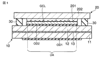
図1に示すように、表示装置は、表示ユニット10と、光線制御素子であるレンズアレイユニット20と、を備えて構成されている。表示ユニット10は、一対の基板すなわち第1基板11と第2基板12とを貼り合わせた構造である。第2基板12は、第1基板11とレンズアレイユニット20との間に配置されている。
As shown in FIG. 1, the display device includes a
この表示ユニット10は、液晶表示パネル、プラズマ表示パネル、有機EL(エレクトロルミネッセンス)表示パネル、電界放出型表示パネルなどで構成されており、特に、種類は問わない。この実施の形態においては、特に、表示ユニット10として液晶表示パネルを適用した例について説明する。
The
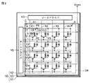
図2及び図3に示すように、液晶表示パネル10は、一対の基板すなわち第1基板(アレイ基板)11及び第2基板(対向基板)12間に液晶層13を保持した構造であり、画像を表示する表示エリアDAを備えている。この表示エリアDAは、マトリクス状に配置された複数の画素PXによって構成されている。
As shown in FIGS. 2 and 3, the liquid
第1基板11は、例えばガラス基板等の光透過性を有する絶縁基板11Aを用いて形成されている。この第1基板11は、絶縁基板11A上において、各画素に駆動信号を供給する配線部を備えている。すなわち、第1基板11は、配線部として、画素PXの行方向に沿って配置された複数の走査線Y(Y1〜Ym)及び複数の補助容量線C(C1〜Cm)、画素PXの列方向に沿って配置されたN本の信号線X(X1〜Xn)、画素PX毎に配置されたスイッチング素子SWなどを備えている。さらに、第1基板11は、各スイッチング素子SWに接続された画素電極PEなどを備えている。走査線Yのそれぞれは、駆動信号(走査信号)を供給するゲートドライバYDに接続されている。信号線Xのそれぞれは、駆動信号(映像信号)を供給するソースドライバXDに接続されている。
The
各スイッチング素子SWは、例えば薄膜トランジスタによって構成されている。このスイッチング素子SWは、各画素PXに対応して走査線Y及び信号線Xの交差部に配置されている。スイッチング素子SWのゲートは、対応する走査線Yに接続されている(あるいは走査線Yと一体的に形成されている)。スイッチング素子SWのソースは、対応する信号線Xに接続されている(あるいは信号線Xと一体的に形成されている)。スイッチング素子SWのドレインは、画素電極PEに電気的に接続されている。 Each switching element SW is composed of, for example, a thin film transistor. The switching element SW is disposed at the intersection of the scanning line Y and the signal line X corresponding to each pixel PX. The gate of the switching element SW is connected to the corresponding scanning line Y (or formed integrally with the scanning line Y). The source of the switching element SW is connected to the corresponding signal line X (or formed integrally with the signal line X). The drain of the switching element SW is electrically connected to the pixel electrode PE.
各画素電極PEは、スイッチング素子SWを覆う絶縁膜IL上に配置されており、絶縁膜ILに形成されたコンタクトホールを介してスイッチング素子SWのドレインと電気的に接続されている。この画素電極PEは、バックライトユニットから放射されたバックライト光を選択的に透過して画像を表示する透過型の液晶表示パネルにおいては、インジウム・ティン・オキサイド(ITO)やインジウム・ジンク・オキサイド(IZO)などの光透過性を有する導電材料によって形成される。また、各画素電極PEは、第2基板12側から入射する外光(フロントライトユニットから放射されたフロントライト光も含む)を選択的に反射して画像を表示する反射型の液晶表示パネルにおいては、アルミニウム(Al)などの光反射性を有する導電材料によって形成される。このような画素電極PEの表面は、液晶層13に含まれる液晶分子の配向を制御するための第1配向膜AL1によって覆われている。
Each pixel electrode PE is disposed on the insulating film IL covering the switching element SW, and is electrically connected to the drain of the switching element SW through a contact hole formed in the insulating film IL. The pixel electrode PE is made of indium tin oxide (ITO) or indium zinc oxide in a transmissive liquid crystal display panel that selectively transmits backlight light emitted from the backlight unit and displays an image. It is formed of a light-transmitting conductive material such as (IZO). Each pixel electrode PE is a reflective liquid crystal display panel that selectively reflects external light (including front light emitted from the front light unit) incident from the
第2基板12は、例えばガラス基板等の光透過性を有する絶縁基板12Aを用いて形成されている。この第2基板12は、絶縁基板12A上において、複数の画素電極PEに対向して配置された対向電極CEなどを備えている。対向電極CEは、光透過性を有する導電材料によって形成されている。このような対向電極CEの表面は、液晶層13に含まれる液晶分子の配向を制御するための第2配向膜AL2によって覆われている。
The
これらの第1基板11及び第2基板12は、画素電極PEと対向電極CEとを対向させた状態で配設され、これらの間にセルギャップを形成する。液晶層13は、第1基板11と第2基板12とのセルギャップに封止された液晶組成物によって形成されている。この実施の形態においては、液晶モードについて特に制限はなく、TN(Twisted Nematic)モード、OCB(Optically Compensated Bend)モード、VA(Vertical Aligned)モード、IPS(In−Plane Switching)モードなどが適用可能である。
The
カラー表示タイプの液晶表示装置では、液晶表示パネル10は、複数種類の画素、例えば赤(R)を表示する赤色画素、緑(G)を表示する緑色画素、青(B)を表示する青色画素を有している。すなわち、赤色画素は、赤色の主波長の光を透過する赤色カラーフィルタを備えている。緑色画素は、緑色の主波長の光を透過する緑色カラーフィルタを備えている。青色画素は、青色の主波長の光を透過する青色カラーフィルタを備えている。これらのカラーフィルタは、第1基板11または第2基板12の主面に配置される。
In the color display type liquid crystal display device, the liquid
各画素PXは、各々画素電極PE及び対向電極CE間に液晶容量CLCを有している。複数の補助容量線C(C1〜Cm)は、各々対応行の画素電極PEに容量結合して補助容量Csを構成する。 Each pixel PX has a liquid crystal capacitor CLC between the pixel electrode PE and the counter electrode CE. The plurality of auxiliary capacitance lines C (C1 to Cm) are capacitively coupled to the pixel electrodes PE in the corresponding rows, respectively, to form the auxiliary capacitance Cs.
透過型の液晶表示パネルを適用した構成においてはバックライトユニットを含み、図3に示すように、表示エリアDAに対応して第1基板11の外面に偏光板を含む第1光学素子OD1が配置され、また、第2基板12の外面にも同様に偏光板を含む第2光学素子OD2が配置されている。
In the configuration using the transmissive liquid crystal display panel, a first optical element OD1 including a backlight unit and including a polarizing plate is disposed on the outer surface of the
レンズアレイユニット20は、例えば図4Aや図4Bなどに示すような形状で構成される。すなわち、レンズアレイユニット20は、基体202と、基体202上に配置されたレンズアレイ層201と、を備えて構成されている。これらのレンズアレイユニット20のレンズアレイ層201は、一方向に並んだ複数のシリンドリカルレンズによって構成されている。ここで、便宜上、走査線が延在する方向と平行な方向をXとし、信号線が延在する方向と平行な方向をYとし、X−Y平面の法線方向(表示ユニット10の厚み方向)をZとする。
The
図4Aに示した例のレンズアレイユニット20においては、各シリンドリカルレンズはその円筒面の母線がY方向に伸びた形状であり、複数のシリンドリカルレンズがX方向に並んでいる。また、図4Bに示した例のレンズアレイユニット20においては、各シリンドリカルレンズはその円筒面の母線がX方向及びY方向に対して傾いた形状であり、複数のシリンドリカルレンズがX方向に並んでいる。
In the
レンズアレイ層201において、シリンドリカルレンズの水平ピッチPsは、表示ユニット10の表示エリアDAにおける行方向(つまりX方向)に一致する方向のピッチである。このレンズアレイ層201は、レンズアレイユニット20が表示ユニット10に対向して配置された際、少なくとも表示エリアDAと対向するような領域にわたって形成されている。つまり、レンズアレイ層201が形成される面積は、表示エリアDAと同等以上に設定される。レンズアレイ層201の厚み(すなわち、基体の表面からレンズのトップ部分までの厚み)は、例えば0.2mm乃至0.5mm程度であり、また、レンズの間の掘り込み量は、例えば0.05mm乃至0.1mm程度であるが、これらの値は設計に応じて種々変更可能である。
In the
基体202は、レンズアレイ層201を支持する平板状のものであって、レンズアレイ層201よりも大きなサイズを有している。この基体202は、例えば0.7mm乃至1.1mm程度の厚さを有しているが、必要に応じてさらに厚い数mm程度のものを適用しても良い。
The
このようなレンズアレイユニット20は、種々の形態が提案され、いずれも適用可能である。すなわち、図5Aに示した例のレンズアレイユニット20は、ガラス製の基体202及びガラス製のレンズアレイ層201によって一体的に形成したものである。つまり、図5Aの例は、ガラス基板の表面に加工を施して直接レンズ形状を形成したものである。このようにガラスによって一体的に形成されたレンズアレイユニット20は、温度変化の影響を受けにくく、安定した性能を維持できるといったメリットがある。
Various types of such
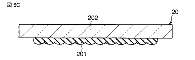
図5Bに示した例のレンズアレイユニット20は、ガラス製の基体202に接着層203を介して樹脂製のレンズアレイ層201を接着したものである。図5Cに示した例のレンズアレイユニット20は、ガラス製の基体202に直接樹脂製のレンズアレイ層201を成型したものである。樹脂製のレンズアレイ層201は、例えばPMMA(ポリメチルメタクリレート)やPC(ポリカーボネート)などの材料によって形成されている。このような樹脂製のレンズアレイ層201は、プレス成型や射出成型により安価に製造できるといったメリットがある。一方で、樹脂材料は、基体202を形成するガラスよりも線膨張係数が大きいため、温度変化の影響を受けやすい。このため、水平ピッチPsの変動を抑制する目的で、レンズアレイ層201は、比較的厚い基体202に貼り付けることが望ましい。基体202の面積はレンズ層201よりもやや大きめにしてあり、余剰部分はレンズアレイユニット20を表示ユニット10に固定するための接着部として利用可能である。
The
このようなレンズアレイユニット20は、支持体30により表示ユニット10に対して所定のギャップを形成した状態で固定されている。すなわち、図1に示したように、レンズアレイユニット20は、レンズアレイ層201側が、表示ユニット10に対向するように配置されている。レンズアレイ層201が観察者側に面する構造を適用することも可能であるが、耐久性や信頼性の確保のために厚い基体202を用いた場合、レンズ焦点距離が長くなるためレンズ設計に制約が出る点や、レンズ凸面による外光反射を防止するためにさらに外側にフェースガラスを設置させると部材点数や重量が増大する。
Such a
特に、この実施の形態においては、表示ユニット10とレンズアレイユニット20との間に所定のギャップを形成するギャップ制御層GCLが配置されている。すなわち、このギャップ制御層GCLは、支持体30によって囲まれた内側の領域に配置され、表示ユニット10における第2基板12の外面に配置された第2光学素子OD2に接触するとともに、レンズアレイユニット20におけるレンズアレイ層201のレンズトップ部分に接触している。このようなギャップ制御層GCLは、表示ユニット10とレンズアレイユニット20との間に均一なギャップを形成するものである。なお、ギャップ制御層GCLは、レンズアレイ層201に接触することからそのレンズ作用に影響を及ぼさないようにするためにも、ギャップ制御層GCLを構成する材料の屈折率は、レンズアレイ層201を構成する材料の屈折率とは異なることが望ましい。
In particular, in this embodiment, a gap control layer GCL that forms a predetermined gap is disposed between the
支持体30は、表示ユニット10の表示エリアDA外において、表示ユニット10とレンズアレイユニット20との間に所定のギャップを形成した状態で固定する。図1に示した例では、レンズアレイ層201は、その表面が表示ユニット10の表面とは接着することなく、表示ユニット10を構成する第2基板12に対して、レンズアレイユニット20の周辺部のみが固定されている。つまり、表示ユニット10とレンズアレイユニット20とは、上述したようなギャップ制御層GCLを挟持した状態で支持体30によって直接固定されており、両者の間の距離が安定的に固定され、表示性能の安定性が確保される。
The
特に、図1に示した例では、レンズアレイユニット20は、表示エリアDAと同等の面積にわたって配置されたレンズアレイ層201を備えており、支持体30は、表示ユニット10の第2基板12と、レンズアレイユニット20の基体202との間に配置されている。
In particular, in the example shown in FIG. 1, the
支持体30は、表示エリアDAを囲む枠状に配置されても良いし、表示エリアDAの外周に点在した柱状に形成されても良い。このような支持体30は、表示ユニット10とレンズアレイユニット20との間の距離を保持するためのスペーサを有している。
The
例えば、支持体30は、金属板、樹脂板、ガラス板などの板状スペーサを有し、表示ユニット10及びレンズアレイユニット20に対してそれぞれ接着剤により接着されている。また、支持体30は、板状スペーサを有するものに限らず、棒状や小片を含むものであってもよい。このとき、接着剤は、熱硬化性樹脂、紫外線硬化性樹脂などが使用可能である。また、支持体30は、表示ユニット10とレンズアレイユニット20との間の距離を保持するためのスペーサを含有する接着剤によって形成してもよい。ここで、接着剤に含有されるスペーサとしては、スペーサビーズやカットファイバ、ミルドファイバなどが使用可能である。このときの接着剤は、熱硬化性樹脂、紫外線硬化性樹脂などが使用可能である。
For example, the
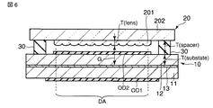
このような構成により、表示エリアDAにおけるレンズ−画素間ギャップを高い精度で均一化することが可能となる。すなわち、図6に本実施形態に対する比較例を示す。この比較例に係る表示装置は、基体202の表面にレンズアレイ層201を有するレンズアレイユニット20と、レンズアレイユニット20に対向して配置された表示ユニット10とを備え、表示ユニット10を構成する2枚の基板のうち、レンズアレイユニット20側の第2基板12に対してレンズアレイユニット20の周辺部が支持体30を介して固定されている。
With such a configuration, the lens-pixel gap in the display area DA can be made uniform with high accuracy. That is, FIG. 6 shows a comparative example for this embodiment. The display device according to this comparative example includes a
レンズ−画素間ギャップとは、レンズアレイユニット20のレンズと表示ユニット10の画素PXとの間の距離である。表示ユニット10として図3に示したような液晶表示パネルを適用する場合、レンズ−画素間ギャップは、より厳密にはレンズアレイユニット20のレンズアレイ層201におけるトップ部分から液晶表示パネル10の液晶層13までの距離に相当する(つまり、レンズアレイ層201と第2光学素子OD2との間の厚み+第2光学素子OD2の厚み+ガラス基板12Aの厚み+対向電極CEの厚み+第2配向膜AL2の厚みがレンズ−画素間ギャップであるが、対向電極CEの厚み及び第2配向膜AL2の厚みは他の構成の厚みに比べて極めて小さいため要求される精度に応じて無視しても良い)。
The lens-pixel gap is a distance between the lens of the
このような表示ユニット10とレンズアレイユニット20との組み合わせにおいては、所望の表示特性を得るためには、少なくとも表示エリアDAにおいて、レンズ−画素間ギャップを均一に制御することが非常に重要である。図6に示した比較例においては、レンズ−画素間ギャップGは以下の式で表される。
In such a combination of the
G=T(substrate)+T(spacer)−T(lens)
ただし、T(substrate)は第2基板12の厚さであり、T(spacer)は支持体30の厚さであり、T(lens)はレンズアレイ層201の厚さである。
G = T (substrate) + T (spacer) −T (lens)
Here, T (substrate) is the thickness of the
このように、図6に示した例では、レンズ−画素間ギャップGのばらつきは、T(substrate)、T(spacer)、T(lens)のばらつきの総和となる。また、レンズアレイユニット20は、周辺部のみ支持体30によって固定されているため、自重によって表示ユニット10側へ反ってしまう。このような現象は、特に画面の大型化に伴って顕著となる。結果として、表示面内においてレンズ−画素間ギャップGが不均一になるといった課題がある。このため、レンズアレイユニット20の自重の大小にかかわらず、レンズ−画素間ギャップGを表示面内で均一にできる構造が要望されている。
As described above, in the example illustrated in FIG. 6, the variation in the lens-pixel gap G is the sum of variations in T (substrate), T (spacer), and T (lens). Further, since the
このような要望に対して、図1に示した本実施形態によれば、表示ユニット10とレンズアレイユニット20との間に、均一な厚さのギャップ制御層GCLを介在させた構造を適用することにより、レンズアレイユニット20の自重による表示ユニット側への反りを抑制することが可能となる。したがって、表示面内において、レンズ−画素間ギャップGをより均一に所望の値に制御することが可能となる。
In response to such a demand, according to the present embodiment shown in FIG. 1, a structure in which a gap control layer GCL having a uniform thickness is interposed between the
図1に示した例では、ギャップ制御層GCLは、シート状のものを適用している。このようなギャップ制御層GCLは、透明な樹脂フィルム、ガラスなどを用いて形成可能である。このようなギャップ制御層GCLの形成方法としては、表示ユニット10のレンズアレイユニット20側の第2光学素子OD2上に接着剤又は糊を介してシートを貼り合せる方式や、液状の樹脂材料をキャスト方式で形成する方式などが適用可能である。
In the example shown in FIG. 1, the gap control layer GCL is a sheet-like material. Such a gap control layer GCL can be formed using a transparent resin film, glass or the like. As a method for forming such a gap control layer GCL, a method in which a sheet is bonded to the second optical element OD2 on the
本実施形態において適用可能なギャップ制御層GCLの形態は、上述したようなシート状のものに限らない。すなわち、ギャップ制御層GCLとしては、表示エリアDAの略全体にわたって配置されたシート状のものに限らず、表示エリアDA内に点在する球状のものや柱状のものを適用しても良い。 The form of the gap control layer GCL applicable in the present embodiment is not limited to the sheet-like form as described above. In other words, the gap control layer GCL is not limited to the sheet-like layer disposed over substantially the entire display area DA, and may be a spherical layer or a column-like layer scattered in the display area DA.
例えば、図7Aに示した例では、ギャップ制御層GCLは、球状スペーサSPによって構成されている。このような球状スペーサSPは、支持体30によって囲まれた内側の領域に配置されており、ガラス、樹脂、シリカ(二酸化珪素)等の材料によって形成可能である。また、球状スペーサSP自身のレンズ作用による表示画像への影響を低減するために、球状スペーサSPは、光吸収性の材料(例えば黒色材料)を用いて形成しても良いが、極めて小さな直径の球状スペーサSPを適用する場合には透明な材料を用いて形成しても良い。
For example, in the example shown in FIG. 7A, the gap control layer GCL is configured by a spherical spacer SP. Such a spherical spacer SP is disposed in an inner region surrounded by the
この球状スペーサSPの直径は、数μmから数百μmまでの範囲で設定可能であるが、球状スペーサSP自身のレンズ作用による表示画像への影響を考慮すると、レンズアレイ層201におけるシリンドリカルレンズの水平ピッチPs(例えば500μm)よりも十分に小さい直径に設定することが望ましい。
The diameter of the spherical spacer SP can be set in a range from several μm to several hundred μm. However, in consideration of the influence on the display image by the lens action of the spherical spacer SP itself, the horizontal length of the cylindrical lens in the
このような構成例においては、第2光学素子OD2上に球状スペーサSPが略均一に散布され、表示ユニット10とレンズアレイユニット20との間で挟持される。このため、ギャップ制御層GCLにおいては、大部分の球状スペーサSPが第2光学素子OD2とレンズアレイ層201のトップ部分との間に挟持される。
In such a configuration example, the spherical spacers SP are distributed substantially uniformly on the second optical element OD2, and are sandwiched between the
図7Bに示した例では、ギャップ制御層GCLは、柱状スペーサCLによって構成されている。このような柱状スペーサCLは、支持体30によって囲まれた内側の領域に配置されており、感光性樹脂材料を用いてフォトリソグラフィ法によって形成可能である。すなわち、このような柱状スペーサCLは、第2光学素子OD2上において、選択的に形成可能であり、図7Bに示した例では、柱状スペーサCLは、その先端部がレンズアレイ層201のトップ部分と接触するように配置されている。
In the example shown in FIG. 7B, the gap control layer GCL is constituted by columnar spacers CL. Such columnar spacers CL are arranged in an inner region surrounded by the
また、図7Cに示した例でも同様に、ギャップ制御層GCLは、柱状スペーサCLによって構成されているが、この柱状スペーサCLは、第2光学素子OD2上において、その先端部がレンズアレイ層201のボトム部分と接触するように配置されている。
Similarly, in the example illustrated in FIG. 7C, the gap control layer GCL is configured by the columnar spacer CL. The columnar spacer CL has a tip end portion on the second optical element OD2 and the
これら、図7A乃至図7Cに示したような各種形態のギャップ制御層GCLを適用した場合であっても、上述した例と同様に、レンズ−画素間ギャップGの表示面内均一性を向上することが可能となり、優れた表示特性を実現することができる。 Even when the gap control layers GCL of various forms as shown in FIGS. 7A to 7C are applied, the in-display uniformity of the lens-pixel gap G is improved as in the above-described example. And excellent display characteristics can be realized.
以上説明した実施の形態においては、表示ユニット10とレンズアレイユニット20とは、表示ユニット10を構成する第2基板12とレンズアレイユニット20を構成する基体202との間に配置された支持体30によって固定されているが、レンズ−画素間ギャップGのばらつきの原因となるパラメータを低減するために、図8Aに示したように、表示ユニット10を構成する2枚の基板のうち、レンズアレイユニット20から遠い側の第1基板11に対して、レンズアレイユニット20の基体202が支持体30を介して固定しても良い。このような構成例においては、レンズ−画素間ギャップGは以下の式で表される。
In the embodiment described above, the
G=T(spacer)−T(lens)
このように、図1に示した例では、レンズ−画素間ギャップGのばらつきは、T(spacer)、T(lens)のばらつきの総和となり、図6に示した比較例の構造と比較すると、レンズ−画素間ギャップGをばらつかせるパラメータが一つ減る。したがって、表示エリアDA内において、ギャップ制御層GCLを配置した効果に加え、さらにレンズ−画素間ギャップGのばらつきを抑えることが可能となり、より均一に所望の値に制御することが可能となる。
G = T (spacer) −T (lens)
Thus, in the example shown in FIG. 1, the variation in the lens-pixel gap G is the sum of the variations in T (spacer) and T (lens). Compared with the structure of the comparative example shown in FIG. One parameter for varying the lens-pixel gap G is reduced. Therefore, in addition to the effect of disposing the gap control layer GCL in the display area DA, it is possible to further suppress variations in the lens-pixel gap G, and to control to a desired value more uniformly.
また、図8Bに示した例では、レンズアレイユニット20は、表示ユニット10の第2基板12よりも大きな面積にわたって配置されたレンズアレイ層201を備えており、支持体30は、表示ユニット10の第1基板11と、レンズアレイユニット20のレンズアレイ層201との間に配置されている。
In the example shown in FIG. 8B, the
図8Bに示した例によれば、表示ユニット10を構成する2枚の基板のうち、レンズアレイユニット20から遠い側の第1基板に対して、レンズアレイユニット20のレンズアレイ層201が支持体30を介して固定されているため、レンズ−画素間ギャップGは以下の式で表される。
According to the example shown in FIG. 8B, the
G=T(spacer)
このように、図8Bに示した例では、レンズ−画素間ギャップGのばらつきは、T(spacer)のばらつきとなり、図8Aに示した実施形態と比較して、レンズ−画素間ギャップGをばらつかせるパラメータがさらに一つ減る。したがって、表示エリアDA内において、ギャップ制御層GCLを配置した効果に加え、さらにレンズ−画素間ギャップGのばらつきをさらに抑えることが可能となり、より均一に所望の値に制御することが可能となる。
G = T (spacer)
As described above, in the example illustrated in FIG. 8B, the variation in the lens-pixel gap G is a variation in T (spacer), and the lens-pixel gap G is different from that in the embodiment illustrated in FIG. 8A. One more parameter can be used. Therefore, in addition to the effect of disposing the gap control layer GCL in the display area DA, it is possible to further suppress the variation in the lens-pixel gap G, and to control to a desired value more uniformly. .
なお、図8A及び図8Bに示した例では、ギャップ制御層GCLとしてシート状のものを適用した場合を図示しているが、これらの例に限らず、図7A乃至図7Cに示した形態のギャップ制御層GCLを適用してもよいことは言うまでもない。 In the example shown in FIGS. 8A and 8B, a case in which a sheet-like material is applied as the gap control layer GCL is illustrated. However, the present invention is not limited to these examples, and the configuration shown in FIGS. 7A to 7C is used. Needless to say, the gap control layer GCL may be applied.
次に、表示装置の一例として、1次元IP方式や多眼方式の立体映像を表示可能な表示装置について説明する。 Next, as an example of a display device, a display device capable of displaying a one-dimensional IP system or multi-view 3D video will be described.
図9は、立体映像表示装置の全体を概略的に示す斜視図である。立体映像表示装置は、要素画像表示部を含む液晶表示パネルなどの表示ユニット10及び光学的開口を有する光線制御素子として機能するレンズアレイユニット20を備えている。レンズアレイユニット20は、要素画像表示部に対向して設けられ、レンズアレイ層の各レンズ主点を基準にした各方向の光線によって立体表示を行う。観察者の想定位置44において、水平画角41と垂直画角42との範囲で、レンズアレイユニット20の前面及び背面の近傍に立体映像が観察可能となる。
FIG. 9 is a perspective view schematically showing the entire stereoscopic video display apparatus. The stereoscopic image display apparatus includes a
図10は、図9に示した立体映像表示装置の表示部を基準にして垂直面内及び水平面内における光線再生範囲を概略的に示す展開図である。図10の(a)に表示ユニット10及びレンズアレイユニット20の正面図、図10の(b)に立体映像表示装置の画像配置を示す平面図、図10の(c)に立体映像表示装置の側面図を示す。図10において、レンズアレイユニット20と視距離面43との間の視距離L、レンズアレイユニット20における水平ピッチPs、レンズアレイユニット20と画素面とのギャップdが定められれば、要素画像水平ピッチPeが視距離面43上の視点からアパーチャ(またはレンズ主点)中心を要素画像表示面(画素面)上に投影した間隔により決定される。符号46は、視点位置と各アパーチャ中心(レンズ主点)とを結ぶ線を示し、視域幅Wは画素面上で要素画像同士が重なり合わないという条件から決定される。平行光線の組を持つ条件の1次元IP方式の場合は、要素画像の水平ピッチの平均値がサブ画素水平ピッチの整数倍よりわずかに大きく、かつレンズアレイユニット20の水平ピッチがサブ画素水平ピッチの整数倍に等しい。多眼方式の場合は、要素画像の水平ピッチがサブ画素水平ピッチの整数倍に等しく、かつレンズアレイユニットの水平ピッチがサブ画素水平ピッチの整数倍よりわずかに小さい。
FIG. 10 is a developed view schematically showing light beam reproduction ranges in the vertical plane and the horizontal plane with reference to the display unit of the stereoscopic video display apparatus shown in FIG. 10 (a) is a front view of the
図11は、立体映像表示装置の一部分の構成を概略的に示す斜視図である。ここでは、液晶表示パネルなどの平面状の要素画像表示部の前面に、シリンドリカルレンズアレイからなるレンズアレイユニット(レンチキュラーシート)20が配置されている場合を示している。図11に示されるように、要素画像表示部には、縦横比が3:1のサブ画素31が横方向(X方向)及び縦方向(Y方向)に夫々直線状にマトリクス状に配置され、サブ画素31は、行方向(X方向)及び列方向(Y方向)に赤(R)、緑(G)、青(B)が交互に並ぶように配列されている。このような色配列は、一般にモザイク配列と呼ばれる。 FIG. 11 is a perspective view schematically showing a configuration of a part of the stereoscopic video display apparatus. Here, a case where a lens array unit (lenticular sheet) 20 formed of a cylindrical lens array is arranged on the front surface of a planar element image display unit such as a liquid crystal display panel is shown. As shown in FIG. 11, in the element image display unit, sub-pixels 31 having an aspect ratio of 3: 1 are arranged in a matrix in a straight line in the horizontal direction (X direction) and the vertical direction (Y direction), respectively. The sub-pixels 31 are arranged so that red (R), green (G), and blue (B) are alternately arranged in the row direction (X direction) and the column direction (Y direction). Such a color arrangement is generally called a mosaic arrangement.
ここに示した例では、9列3行のサブ画素31で1つの立体映像表示時の実効画素32(黒枠で示されている)が構成される。このような表示部の構造では、立体映像表示時の実効画素32が27サブ画素からなることから、1視差に3色成分が必要であるとすると、X方向に9視差を与える立体画像・映像表示が可能となる。なお、実効画素とは立体表示時の解像度を決定する最小単位のサブ画素群をさし、要素画像とは1つのレンズに対応する視差成分画像の集合をさす。したがって、シリンドリカルレンズを使用する構成の立体映像表示装置の場合は、1つの要素画像は、縦方向に並ぶ多数の実効画素を含んでいる。
In the example shown here, the effective pixels 32 (indicated by a black frame) at the time of stereoscopic image display are configured by the sub-pixels 31 of 9 columns and 3 rows. In such a structure of the display unit, since the
なお、この発明は、上記実施形態そのものに限定されるものではなく、その実施の段階ではその要旨を逸脱しない範囲で構成要素を変形して具体化できる。また、上記実施形態に開示されている複数の構成要素の適宜な組み合せにより種々の発明を形成できる。例えば、実施形態に示される全構成要素から幾つかの構成要素を削除してもよい。更に、異なる実施形態に亘る構成要素を適宜組み合せてもよい。 In addition, this invention is not limited to the said embodiment itself, In the stage of implementation, it can change and implement a component within the range which does not deviate from the summary. Further, various inventions can be formed by appropriately combining a plurality of constituent elements disclosed in the embodiment. For example, some components may be deleted from all the components shown in the embodiment. Furthermore, you may combine suitably the component covering different embodiment.
例えば、この発明は、立体映像表示装置として構成する場合に限らず、表示パネルとレンズアレイユニットとを所定のギャップで固定して構成される他の表示装置、例えば2以上の方位で異なる画像を同時に表示可能なマルチビューディスプレイを構成する場合にも適用可能である。 For example, the present invention is not limited to the case where it is configured as a stereoscopic video display device, but other display devices configured by fixing the display panel and the lens array unit at a predetermined gap, for example, images different in two or more directions. The present invention can also be applied to the case of configuring a multi-view display that can display simultaneously.
DA…表示エリア PX…画素 G…レンズ−画素間ギャップ GCL…ギャップ制御層 SP…球状スペーサ CL…柱状スペーサ
10…表示ユニット(液晶表示パネル) 11…第1基板(アレイ基板) 12…第2基板(対向基板) 13…液晶層 20…レンズアレイユニット 30…支持体
201…レンズアレイ層 202…基体 203…接着層
DA ... display area PX ... pixel G ... lens-pixel gap GCL ... gap control layer SP ... spherical spacer CL ...
Claims (8)
第1基板及びこの第1基板と前記レンズアレイユニットとの間に配置された第2基板を貼り合わせた構造であり、マトリクス状に配列された画素によって構成された表示エリアを有する表示ユニットと、
前記表示エリアに配置され、前記表示ユニットの前記第2基板と前記レンズアレイユニットとの間に所定のギャップを形成するギャップ制御層と、
前記表示ユニットの表示エリア外において、前記表示ユニットの前記第1基板と前記レンズアレイユニットとを固定する支持体と、
を備えたことを特徴とする表示装置。 A lens array unit;
A display unit having a first substrate and a second substrate disposed between the first substrate and the lens array unit, the display unit having a display area composed of pixels arranged in a matrix;
A gap control layer disposed in the display area and forming a predetermined gap between the second substrate of the display unit and the lens array unit;
A support for fixing the first substrate of the display unit and the lens array unit outside the display area of the display unit;
A display device comprising:
前記レンズアレイユニットは、ガラス製の前記基体及び前記レンズアレイ層によって一体的に形成されたもの、ガラス製の前記基体に接着層を介して樹脂製の前記レンズアレイ層を接着したもの、及び、ガラス製の前記基体に直接樹脂製の前記レンズアレイ層を成型したもののいずれかであることを特徴とする請求項1に記載の表示装置。 The lens array unit includes a base and a lens array layer facing at least the display area on the base,
The lens array unit is integrally formed by the glass base and the lens array layer, the glass base is bonded to the resin lens array layer through an adhesive layer, and 2. The display device according to claim 1, wherein the lens array layer made of resin is directly molded on the glass substrate.
前記支持体は、前記第1基板と前記基体とを固定することを特徴とする請求項1に記載の表示装置。The display device according to claim 1, wherein the support fixes the first substrate and the base body.
前記支持体は、前記第1基板と前記レンズアレイ層とを固定することを特徴とする請求項1に記載の表示装置。The display device according to claim 1, wherein the support fixes the first substrate and the lens array layer.
Priority Applications (2)
| Application Number | Priority Date | Filing Date | Title |
|---|---|---|---|
| JP2007024430A JP5024992B2 (en) | 2007-02-02 | 2007-02-02 | Display device |
| US11/971,964 US7675681B2 (en) | 2007-02-02 | 2008-01-10 | Display device |
Applications Claiming Priority (1)
| Application Number | Priority Date | Filing Date | Title |
|---|---|---|---|
| JP2007024430A JP5024992B2 (en) | 2007-02-02 | 2007-02-02 | Display device |
Publications (3)
| Publication Number | Publication Date |
|---|---|
| JP2008191325A JP2008191325A (en) | 2008-08-21 |
| JP2008191325A5 JP2008191325A5 (en) | 2010-03-11 |
| JP5024992B2 true JP5024992B2 (en) | 2012-09-12 |
Family
ID=39675899
Family Applications (1)
| Application Number | Title | Priority Date | Filing Date |
|---|---|---|---|
| JP2007024430A Active JP5024992B2 (en) | 2007-02-02 | 2007-02-02 | Display device |
Country Status (2)
| Country | Link |
|---|---|
| US (1) | US7675681B2 (en) |
| JP (1) | JP5024992B2 (en) |
Families Citing this family (83)
| Publication number | Priority date | Publication date | Assignee | Title |
|---|---|---|---|---|
| JP2009115920A (en) * | 2007-11-02 | 2009-05-28 | Toshiba Matsushita Display Technology Co Ltd | Display device |
| US8866920B2 (en) | 2008-05-20 | 2014-10-21 | Pelican Imaging Corporation | Capturing and processing of images using monolithic camera array with heterogeneous imagers |
| EP3328048B1 (en) | 2008-05-20 | 2021-04-21 | FotoNation Limited | Capturing and processing of images using monolithic camera array with heterogeneous imagers |
| US11792538B2 (en) | 2008-05-20 | 2023-10-17 | Adeia Imaging Llc | Capturing and processing of images including occlusions focused on an image sensor by a lens stack array |
| GB2461907A (en) * | 2008-07-17 | 2010-01-20 | Sharp Kk | Angularly restricted display |
| JP2010128277A (en) * | 2008-11-28 | 2010-06-10 | Oki Data Corp | Lens array unit, optical head and information apparatus |
| JP5511180B2 (en) * | 2008-12-19 | 2014-06-04 | キヤノン株式会社 | Solid-state imaging device manufacturing method and solid-state imaging device |
| JP2011051245A (en) * | 2009-09-02 | 2011-03-17 | Seiko Epson Corp | Exposure head, and image forming apparatus |
| EP2502115A4 (en) | 2009-11-20 | 2013-11-06 | Pelican Imaging Corp | Capturing and processing of images using monolithic camera array with heterogeneous imagers |
| JP2013145254A (en) * | 2010-04-21 | 2013-07-25 | Asahi Glass Co Ltd | Glass lenticular lens structure and stereoscopic display device, and method of manufacturing glass lenticular lens structure |
| SG10201503516VA (en) | 2010-05-12 | 2015-06-29 | Pelican Imaging Corp | Architectures for imager arrays and array cameras |
| EP3557311A1 (en) * | 2010-07-28 | 2019-10-23 | Koninklijke Philips N.V. | Optical beam deflection arrangement and multi-view display having the same |
| JP5149356B2 (en) * | 2010-09-08 | 2013-02-20 | 株式会社東芝 | Stereoscopic image display device |
| JP5222918B2 (en) | 2010-09-29 | 2013-06-26 | 株式会社ジャパンディスプレイセントラル | Liquid crystal display |
| US8878950B2 (en) | 2010-12-14 | 2014-11-04 | Pelican Imaging Corporation | Systems and methods for synthesizing high resolution images using super-resolution processes |
| US9268175B2 (en) * | 2011-03-28 | 2016-02-23 | Sharp Kabushiki Kaisha | Display device |
| JP5377555B2 (en) | 2011-03-29 | 2013-12-25 | 株式会社ジャパンディスプレイ | Liquid crystal display |
| JP2012208324A (en) * | 2011-03-30 | 2012-10-25 | Citizen Finetech Miyota Co Ltd | Liquid crystal element |
| KR101973822B1 (en) | 2011-05-11 | 2019-04-29 | 포토네이션 케이맨 리미티드 | Systems and methods for transmitting and receiving array camera image data |
| TWI565119B (en) * | 2011-05-27 | 2017-01-01 | 半導體能源研究所股份有限公司 | Method of manufacturing light-emitting device and light-emitting device |
| US20130265459A1 (en) | 2011-06-28 | 2013-10-10 | Pelican Imaging Corporation | Optical arrangements for use with an array camera |
| JP2014521117A (en) | 2011-06-28 | 2014-08-25 | ペリカン イメージング コーポレイション | Optical array for use with array cameras |
| WO2013043751A1 (en) | 2011-09-19 | 2013-03-28 | Pelican Imaging Corporation | Systems and methods for controlling aliasing in images captured by an array camera for use in super resolution processing using pixel apertures |
| IN2014CN02708A (en) | 2011-09-28 | 2015-08-07 | Pelican Imaging Corp | |
| US20130169885A1 (en) * | 2011-12-28 | 2013-07-04 | Masataka Tsunemi | Display device and television receiver |
| WO2013126578A1 (en) | 2012-02-21 | 2013-08-29 | Pelican Imaging Corporation | Systems and methods for the manipulation of captured light field image data |
| JP6008233B2 (en) * | 2012-03-23 | 2016-10-19 | Nltテクノロジー株式会社 | Image display device |
| US9210392B2 (en) | 2012-05-01 | 2015-12-08 | Pelican Imaging Coporation | Camera modules patterned with pi filter groups |
| WO2014005123A1 (en) | 2012-06-28 | 2014-01-03 | Pelican Imaging Corporation | Systems and methods for detecting defective camera arrays, optic arrays, and sensors |
| US20140002674A1 (en) | 2012-06-30 | 2014-01-02 | Pelican Imaging Corporation | Systems and Methods for Manufacturing Camera Modules Using Active Alignment of Lens Stack Arrays and Sensors |
| US9211481B2 (en) * | 2012-07-27 | 2015-12-15 | Nb Tech Inc. | Visual display system and method of constructing a high-gain reflective beam-splitter |
| WO2014031795A1 (en) | 2012-08-21 | 2014-02-27 | Pelican Imaging Corporation | Systems and methods for parallax detection and correction in images captured using array cameras |
| US20140055632A1 (en) | 2012-08-23 | 2014-02-27 | Pelican Imaging Corporation | Feature based high resolution motion estimation from low resolution images captured using an array source |
| US9214013B2 (en) | 2012-09-14 | 2015-12-15 | Pelican Imaging Corporation | Systems and methods for correcting user identified artifacts in light field images |
| EP2901671A4 (en) | 2012-09-28 | 2016-08-24 | Pelican Imaging Corp | Generating images from light fields utilizing virtual viewpoints |
| WO2014078443A1 (en) | 2012-11-13 | 2014-05-22 | Pelican Imaging Corporation | Systems and methods for array camera focal plane control |
| US9462164B2 (en) | 2013-02-21 | 2016-10-04 | Pelican Imaging Corporation | Systems and methods for generating compressed light field representation data using captured light fields, array geometry, and parallax information |
| US9374512B2 (en) | 2013-02-24 | 2016-06-21 | Pelican Imaging Corporation | Thin form factor computational array cameras and modular array cameras |
| US9638883B1 (en) | 2013-03-04 | 2017-05-02 | Fotonation Cayman Limited | Passive alignment of array camera modules constructed from lens stack arrays and sensors based upon alignment information obtained during manufacture of array camera modules using an active alignment process |
| WO2014138697A1 (en) | 2013-03-08 | 2014-09-12 | Pelican Imaging Corporation | Systems and methods for high dynamic range imaging using array cameras |
| US8866912B2 (en) | 2013-03-10 | 2014-10-21 | Pelican Imaging Corporation | System and methods for calibration of an array camera using a single captured image |
| US9521416B1 (en) | 2013-03-11 | 2016-12-13 | Kip Peli P1 Lp | Systems and methods for image data compression |
| US9888194B2 (en) | 2013-03-13 | 2018-02-06 | Fotonation Cayman Limited | Array camera architecture implementing quantum film image sensors |
| US9519972B2 (en) | 2013-03-13 | 2016-12-13 | Kip Peli P1 Lp | Systems and methods for synthesizing images from image data captured by an array camera using restricted depth of field depth maps in which depth estimation precision varies |
| WO2014164550A2 (en) | 2013-03-13 | 2014-10-09 | Pelican Imaging Corporation | System and methods for calibration of an array camera |
| US9106784B2 (en) | 2013-03-13 | 2015-08-11 | Pelican Imaging Corporation | Systems and methods for controlling aliasing in images captured by an array camera for use in super-resolution processing |
| WO2014159779A1 (en) | 2013-03-14 | 2014-10-02 | Pelican Imaging Corporation | Systems and methods for reducing motion blur in images or video in ultra low light with array cameras |
| US9100586B2 (en) | 2013-03-14 | 2015-08-04 | Pelican Imaging Corporation | Systems and methods for photometric normalization in array cameras |
| US10122993B2 (en) | 2013-03-15 | 2018-11-06 | Fotonation Limited | Autofocus system for a conventional camera that uses depth information from an array camera |
| US9497429B2 (en) | 2013-03-15 | 2016-11-15 | Pelican Imaging Corporation | Extended color processing on pelican array cameras |
| EP2973476A4 (en) | 2013-03-15 | 2017-01-18 | Pelican Imaging Corporation | Systems and methods for stereo imaging with camera arrays |
| US9497370B2 (en) | 2013-03-15 | 2016-11-15 | Pelican Imaging Corporation | Array camera architecture implementing quantum dot color filters |
| US9445003B1 (en) | 2013-03-15 | 2016-09-13 | Pelican Imaging Corporation | Systems and methods for synthesizing high resolution images using image deconvolution based on motion and depth information |
| US9633442B2 (en) | 2013-03-15 | 2017-04-25 | Fotonation Cayman Limited | Array cameras including an array camera module augmented with a separate camera |
| JP2013238859A (en) * | 2013-06-10 | 2013-11-28 | Nippon Steel & Sumikin Chemical Co Ltd | Ink composition for inkjet color filter superior in storage stability, and cured film of inkjet color filter and color filter obtained by using ink composition |
| US9898856B2 (en) | 2013-09-27 | 2018-02-20 | Fotonation Cayman Limited | Systems and methods for depth-assisted perspective distortion correction |
| US9185276B2 (en) | 2013-11-07 | 2015-11-10 | Pelican Imaging Corporation | Methods of manufacturing array camera modules incorporating independently aligned lens stacks |
| US10119808B2 (en) | 2013-11-18 | 2018-11-06 | Fotonation Limited | Systems and methods for estimating depth from projected texture using camera arrays |
| WO2015081279A1 (en) | 2013-11-26 | 2015-06-04 | Pelican Imaging Corporation | Array camera configurations incorporating multiple constituent array cameras |
| US10089740B2 (en) | 2014-03-07 | 2018-10-02 | Fotonation Limited | System and methods for depth regularization and semiautomatic interactive matting using RGB-D images |
| US9247117B2 (en) | 2014-04-07 | 2016-01-26 | Pelican Imaging Corporation | Systems and methods for correcting for warpage of a sensor array in an array camera module by introducing warpage into a focal plane of a lens stack array |
| US9521319B2 (en) | 2014-06-18 | 2016-12-13 | Pelican Imaging Corporation | Array cameras and array camera modules including spectral filters disposed outside of a constituent image sensor |
| JP2017531976A (en) | 2014-09-29 | 2017-10-26 | フォトネイション ケイマン リミテッド | System and method for dynamically calibrating an array camera |
| CN104360545B (en) * | 2014-12-03 | 2018-02-06 | 京东方科技集团股份有限公司 | A kind of display panel, display device |
| US9942474B2 (en) | 2015-04-17 | 2018-04-10 | Fotonation Cayman Limited | Systems and methods for performing high speed video capture and depth estimation using array cameras |
| CN104865619B (en) | 2015-06-05 | 2016-08-24 | 京东方科技集团股份有限公司 | A kind of antireflection film, its preparation method, display floater and display device |
| RU2617003C1 (en) * | 2015-11-05 | 2017-04-19 | Самсунг Электроникс Ко., Лтд. | Light guide plate and backlight device containing it |
| US10482618B2 (en) | 2017-08-21 | 2019-11-19 | Fotonation Limited | Systems and methods for hybrid depth regularization |
| CN107991782B (en) * | 2017-11-06 | 2021-01-05 | 维瑟运动国际有限公司 | Naked eye 3D display device |
| JP7187838B2 (en) * | 2018-06-29 | 2022-12-13 | セイコーエプソン株式会社 | head mounted display |
| TWI708222B (en) * | 2019-02-18 | 2020-10-21 | 友達光電股份有限公司 | Display panel |
| MX2022003020A (en) | 2019-09-17 | 2022-06-14 | Boston Polarimetrics Inc | Systems and methods for surface modeling using polarization cues. |
| DE112020004813B4 (en) | 2019-10-07 | 2023-02-09 | Boston Polarimetrics, Inc. | System for expanding sensor systems and imaging systems with polarization |
| CN114787648B (en) | 2019-11-30 | 2023-11-10 | 波士顿偏振测定公司 | Systems and methods for transparent object segmentation using polarization cues |
| US11195303B2 (en) | 2020-01-29 | 2021-12-07 | Boston Polarimetrics, Inc. | Systems and methods for characterizing object pose detection and measurement systems |
| JP2023511747A (en) | 2020-01-30 | 2023-03-22 | イントリンジック イノベーション エルエルシー | Systems and methods for synthesizing data for training statistical models with different imaging modalities, including polarization imaging |
| US11953700B2 (en) | 2020-05-27 | 2024-04-09 | Intrinsic Innovation Llc | Multi-aperture polarization optical systems using beam splitters |
| US11808959B2 (en) * | 2020-08-11 | 2023-11-07 | Himax Technologies Limited | Optical element and wafer level optical module |
| KR20230132475A (en) * | 2021-01-28 | 2023-09-15 | 소니그룹주식회사 | Arrays and stereoscopic displays |
| US11954886B2 (en) | 2021-04-15 | 2024-04-09 | Intrinsic Innovation Llc | Systems and methods for six-degree of freedom pose estimation of deformable objects |
| US11290658B1 (en) | 2021-04-15 | 2022-03-29 | Boston Polarimetrics, Inc. | Systems and methods for camera exposure control |
| US11689813B2 (en) | 2021-07-01 | 2023-06-27 | Intrinsic Innovation Llc | Systems and methods for high dynamic range imaging using crossed polarizers |
| CN115440145A (en) * | 2022-09-30 | 2022-12-06 | 京东方科技集团股份有限公司 | Display module and display device |
Family Cites Families (7)
| Publication number | Priority date | Publication date | Assignee | Title |
|---|---|---|---|---|
| US5956001A (en) * | 1996-03-15 | 1999-09-21 | Sharp Kabushiki Kaisha | Image display device |
| US6219113B1 (en) * | 1996-12-17 | 2001-04-17 | Matsushita Electric Industrial Co., Ltd. | Method and apparatus for driving an active matrix display panel |
| JPH11202313A (en) | 1998-01-19 | 1999-07-30 | Matsushita Electron Corp | Liquid crystal display element |
| JP2003121609A (en) * | 2001-10-11 | 2003-04-23 | Hitachi Ltd | Optical sheet and display device equipped with the same |
| JP4293013B2 (en) * | 2003-02-28 | 2009-07-08 | 日本電気株式会社 | Image display device and manufacturing method thereof |
| JP2006039265A (en) | 2004-07-28 | 2006-02-09 | Seiko Epson Corp | Microlens array plate, its manufacturing method, electrooptical device, and electronic equipment |
| US7800825B2 (en) * | 2006-12-04 | 2010-09-21 | 3M Innovative Properties Company | User interface including composite images that float |
-
2007
- 2007-02-02 JP JP2007024430A patent/JP5024992B2/en active Active
-
2008
- 2008-01-10 US US11/971,964 patent/US7675681B2/en active Active
Also Published As
| Publication number | Publication date |
|---|---|
| US7675681B2 (en) | 2010-03-09 |
| JP2008191325A (en) | 2008-08-21 |
| US20080186572A1 (en) | 2008-08-07 |
Similar Documents
| Publication | Publication Date | Title |
|---|---|---|
| JP5024992B2 (en) | Display device | |
| JP5596625B2 (en) | Display device | |
| US7630131B2 (en) | Image display apparatus and optical member therefor | |
| US9158120B2 (en) | Image display apparatus and variable lens array | |
| JP5877979B2 (en) | Image display device using diffraction element | |
| JP5301283B2 (en) | Display device | |
| US9638964B2 (en) | Liquid crystal lens and three-dimensional display device | |
| CN110286525B (en) | Display substrate, display panel and display device | |
| JP5039055B2 (en) | Switchable autostereoscopic display device | |
| RU2589249C2 (en) | Optical beam deflection device and multi-view display device comprising same | |
| TW201418777A (en) | Display device | |
| JP2008089906A (en) | Lens array unit and stereoscopic video display device equipped therewith | |
| JPWO2014196125A1 (en) | Image display device and liquid crystal lens | |
| TWI417574B (en) | Zoom lens array and switchable two and three dimensional display | |
| KR20150142891A (en) | 3d display apparatus | |
| JP2012531617A (en) | Autostereoscopic display device | |
| JP2009115920A (en) | Display device | |
| JP2006126721A (en) | Liquid crystal optical element array and liquid crystal device | |
| KR102134595B1 (en) | Three-dimension display apparatus | |
| JP2009198830A (en) | Display | |
| JP2010014881A (en) | Optical member, electro-optical apparatus and electronic device | |
| JP2008139793A (en) | Display device | |
| JP2010044206A (en) | Display device | |
| JP2009047759A (en) | Display device | |
| CN102449539A (en) | Liquid chrystal display device with focusing arrangement |
Legal Events
| Date | Code | Title | Description |
|---|---|---|---|
| A521 | Request for written amendment filed |
Free format text: JAPANESE INTERMEDIATE CODE: A523 Effective date: 20100125 |
|
| A621 | Written request for application examination |
Free format text: JAPANESE INTERMEDIATE CODE: A621 Effective date: 20100125 |
|
| A977 | Report on retrieval |
Free format text: JAPANESE INTERMEDIATE CODE: A971007 Effective date: 20110831 |
|
| A131 | Notification of reasons for refusal |
Free format text: JAPANESE INTERMEDIATE CODE: A131 Effective date: 20110906 |
|
| A521 | Request for written amendment filed |
Free format text: JAPANESE INTERMEDIATE CODE: A523 Effective date: 20111102 |
|
| TRDD | Decision of grant or rejection written | ||
| A01 | Written decision to grant a patent or to grant a registration (utility model) |
Free format text: JAPANESE INTERMEDIATE CODE: A01 Effective date: 20120522 |
|
| A01 | Written decision to grant a patent or to grant a registration (utility model) |
Free format text: JAPANESE INTERMEDIATE CODE: A01 |
|
| RD04 | Notification of resignation of power of attorney |
Free format text: JAPANESE INTERMEDIATE CODE: A7424 Effective date: 20120529 |
|
| A61 | First payment of annual fees (during grant procedure) |
Free format text: JAPANESE INTERMEDIATE CODE: A61 Effective date: 20120618 |
|
| FPAY | Renewal fee payment (event date is renewal date of database) |
Free format text: PAYMENT UNTIL: 20150629 Year of fee payment: 3 |
|
| R150 | Certificate of patent or registration of utility model |
Ref document number: 5024992 Country of ref document: JP Free format text: JAPANESE INTERMEDIATE CODE: R150 Free format text: JAPANESE INTERMEDIATE CODE: R150 |
|
| R250 | Receipt of annual fees |
Free format text: JAPANESE INTERMEDIATE CODE: R250 |
|
| R250 | Receipt of annual fees |
Free format text: JAPANESE INTERMEDIATE CODE: R250 |
|
| R250 | Receipt of annual fees |
Free format text: JAPANESE INTERMEDIATE CODE: R250 |
|
| R250 | Receipt of annual fees |
Free format text: JAPANESE INTERMEDIATE CODE: R250 |
|
| R250 | Receipt of annual fees |
Free format text: JAPANESE INTERMEDIATE CODE: R250 |
|
| R250 | Receipt of annual fees |
Free format text: JAPANESE INTERMEDIATE CODE: R250 |
|
| S111 | Request for change of ownership or part of ownership |
Free format text: JAPANESE INTERMEDIATE CODE: R313111 |
|
| R350 | Written notification of registration of transfer |
Free format text: JAPANESE INTERMEDIATE CODE: R350 |
|
| R250 | Receipt of annual fees |
Free format text: JAPANESE INTERMEDIATE CODE: R250 |
|
| R250 | Receipt of annual fees |
Free format text: JAPANESE INTERMEDIATE CODE: R250 |
|
| R250 | Receipt of annual fees |
Free format text: JAPANESE INTERMEDIATE CODE: R250 |