JP7007092B2 - Data addressing method of memory device, memory device and memory module - Google Patents
Data addressing method of memory device, memory device and memory module Download PDFInfo
- Publication number
- JP7007092B2 JP7007092B2 JP2017028878A JP2017028878A JP7007092B2 JP 7007092 B2 JP7007092 B2 JP 7007092B2 JP 2017028878 A JP2017028878 A JP 2017028878A JP 2017028878 A JP2017028878 A JP 2017028878A JP 7007092 B2 JP7007092 B2 JP 7007092B2
- Authority
- JP
- Japan
- Prior art keywords
- row
- address
- subset
- column
- address bits
- Prior art date
- Legal status (The legal status is an assumption and is not a legal conclusion. Google has not performed a legal analysis and makes no representation as to the accuracy of the status listed.)
- Active
Links
Images


Classifications
-
- G—PHYSICS
- G11—INFORMATION STORAGE
- G11C—STATIC STORES
- G11C8/00—Arrangements for selecting an address in a digital store
- G11C8/08—Word line control circuits, e.g. drivers, boosters, pull-up circuits, pull-down circuits, precharging circuits, for word lines
-
- G—PHYSICS
- G11—INFORMATION STORAGE
- G11C—STATIC STORES
- G11C7/00—Arrangements for writing information into, or reading information out from, a digital store
- G11C7/10—Input/output [I/O] data interface arrangements, e.g. I/O data control circuits, I/O data buffers
- G11C7/1015—Read-write modes for single port memories, i.e. having either a random port or a serial port
- G11C7/1018—Serial bit line access mode, e.g. using bit line address shift registers, bit line address counters, bit line burst counters
-
- G—PHYSICS
- G11—INFORMATION STORAGE
- G11C—STATIC STORES
- G11C11/00—Digital stores characterised by the use of particular electric or magnetic storage elements; Storage elements therefor
- G11C11/21—Digital stores characterised by the use of particular electric or magnetic storage elements; Storage elements therefor using electric elements
- G11C11/34—Digital stores characterised by the use of particular electric or magnetic storage elements; Storage elements therefor using electric elements using semiconductor devices
- G11C11/40—Digital stores characterised by the use of particular electric or magnetic storage elements; Storage elements therefor using electric elements using semiconductor devices using transistors
- G11C11/401—Digital stores characterised by the use of particular electric or magnetic storage elements; Storage elements therefor using electric elements using semiconductor devices using transistors forming cells needing refreshing or charge regeneration, i.e. dynamic cells
- G11C11/4063—Auxiliary circuits, e.g. for addressing, decoding, driving, writing, sensing or timing
- G11C11/407—Auxiliary circuits, e.g. for addressing, decoding, driving, writing, sensing or timing for memory cells of the field-effect type
- G11C11/408—Address circuits
-
- G—PHYSICS
- G11—INFORMATION STORAGE
- G11C—STATIC STORES
- G11C13/00—Digital stores characterised by the use of storage elements not covered by groups G11C11/00, G11C23/00, or G11C25/00
- G11C13/0002—Digital stores characterised by the use of storage elements not covered by groups G11C11/00, G11C23/00, or G11C25/00 using resistive RAM [RRAM] elements
- G11C13/0021—Auxiliary circuits
- G11C13/0023—Address circuits or decoders
- G11C13/0026—Bit-line or column circuits
-
- G—PHYSICS
- G11—INFORMATION STORAGE
- G11C—STATIC STORES
- G11C13/00—Digital stores characterised by the use of storage elements not covered by groups G11C11/00, G11C23/00, or G11C25/00
- G11C13/0002—Digital stores characterised by the use of storage elements not covered by groups G11C11/00, G11C23/00, or G11C25/00 using resistive RAM [RRAM] elements
- G11C13/0021—Auxiliary circuits
- G11C13/0023—Address circuits or decoders
- G11C13/0028—Word-line or row circuits
-
- G—PHYSICS
- G11—INFORMATION STORAGE
- G11C—STATIC STORES
- G11C13/00—Digital stores characterised by the use of storage elements not covered by groups G11C11/00, G11C23/00, or G11C25/00
- G11C13/0002—Digital stores characterised by the use of storage elements not covered by groups G11C11/00, G11C23/00, or G11C25/00 using resistive RAM [RRAM] elements
- G11C13/0021—Auxiliary circuits
- G11C13/0069—Writing or programming circuits or methods
-
- G—PHYSICS
- G11—INFORMATION STORAGE
- G11C—STATIC STORES
- G11C8/00—Arrangements for selecting an address in a digital store
- G11C8/04—Arrangements for selecting an address in a digital store using a sequential addressing device, e.g. shift register, counter
-
- G—PHYSICS
- G11—INFORMATION STORAGE
- G11C—STATIC STORES
- G11C8/00—Arrangements for selecting an address in a digital store
- G11C8/06—Address interface arrangements, e.g. address buffers
-
- G—PHYSICS
- G11—INFORMATION STORAGE
- G11C—STATIC STORES
- G11C8/00—Arrangements for selecting an address in a digital store
- G11C8/12—Group selection circuits, e.g. for memory block selection, chip selection, array selection
-
- G—PHYSICS
- G11—INFORMATION STORAGE
- G11C—STATIC STORES
- G11C8/00—Arrangements for selecting an address in a digital store
- G11C8/18—Address timing or clocking circuits; Address control signal generation or management, e.g. for row address strobe [RAS] or column address strobe [CAS] signals
Description
本発明はメモリ装置のデータアドレッシング方法に関し、特に追加的なピンの増加又はピン形成費用の増加無しで高容量SDRAMライクメモリのアドレッシング方法を提供するメモリ装置とのそのデータアドレッシング方法及びメモリモジュールに関する。 The present invention relates to a data addressing method for a memory device, particularly to a data addressing method and a memory module with a memory device that provides a method for addressing a high capacity SDRAM-like memory without additional pin increase or pin formation cost increase.
JEDEC DDR4 SDRAM標準で、CID(チップID、又はランク)のために3つのピンが、バンクのために4つのピンが、行と列(命令語に依存的な)のためには18個の共有されるピンが存在する(命令語に依存)。
現在のピン使用方式とアドレッシング方式とは、DRAMチップデータサイズ、幅、及び構成の正確な組み合わせが選択されて組み立てられたことを仮定すれば(そうでない場合、DIMMの容量が低くなり、アドレッシング可能な領域が減少する結果をもたらす)、DIMM(Dual Inline Memory Module、1つのパッケージに複数のDRAMチップの集合)当たり256GBまでの容量を支援することができる。
In the JEDEC DDR4 SDRAM standard, 3 pins for CID (chip ID or rank), 4 pins for banks, 18 shares for rows and columns (instruction dependent). There is a pin to be used (depending on the command word).
Current pin usage and addressing schemes assume that the correct combination of DRAM chip data size, width, and configuration has been selected and assembled (otherwise the DIMM capacity will be low and addressing is possible. Can support capacities up to 256 GB per DIMM (Dual Inline Memory Module, a collection of multiple DRAM chips in one package).
しかしながら、これよりさらに大きいモジュール容量又はアドレッシング可能性は支援されないという問題がある(例えば、メモリがモジュールに物理的に追加されたとしてもメモリはアドレッシングが不可である)。 However, there is the problem that even larger module capacities or addressing possibilities are not supported (eg, memory is not addressable even if memory is physically added to the module).
本発明は上記従来のメモリ装置における問題点に鑑みてなされたものであって、本発明の目的は、ピン費用又はピン数の増加無しで高容量SDRAMライクメモリのアドレッシング方法を提供できるメモリ装置とのそのデータアドレッシング方法及びメモリモジュールを提供することにある。 The present invention has been made in view of the above-mentioned problems in the conventional memory device, and an object of the present invention is a memory device capable of providing an addressing method for a high-capacity SDRAM-like memory without increasing the pin cost or the number of pins. To provide its data addressing method and memory module.
本発明の実施形態は、SDRAM命令語、タイミング、及び構造を提供する。
一例として、本発明はピン費用又はピン数の増加無しで高容量SDRAMライクメモリのアドレッシング方法及びシステムを提供するためのものである。
本発明のその他の特徴によれば、本発明はSDRAM-like(例えば、DDR4)のアドレスピン標準を維持しながら、高容量メモリモジュールを支援するためのものである。
本発明の他の特徴は、アクティブ命令語(ACT+)又は読出し/書込み命令語(RD/WR+)の拡張をためのことである。
本発明のその他の特徴は、バックツーバック(back to back)RAS/CAS(行アドレスストロボ/列アドレスストロボ)命令語、バックツーバックCAS/CAS、及びタイミング調整のためのことである。
その他の本発明の特徴は、命令語調整及び装置再構成を含むマルチ行又はマルチ列バッファ構造を提供するためのことである。
Embodiments of the invention provide SDRAM commands, timings, and structures.
As an example, the present invention is intended to provide addressing methods and systems for high capacity SDRAM-like memories without pin costs or increased pin counts.
According to other features of the invention, the invention is for supporting high capacity memory modules while maintaining the address pin standard of SDRAM-like (eg DDR4).
Another feature of the present invention is to extend the active instruction word (ACT +) or the read / write instruction word (RD / WR +).
Other features of the invention are for back-to-back RAS / CAS (row address strobe / column address strobe) instructions, back-to-back CAS / CAS, and timing adjustments.
Another feature of the present invention is to provide a multi-row or multi-column buffer structure including instruction word adjustment and device reconstruction.
上記目的を達成するためになされた本発明によるメモリ装置のデータアドレッシング方法は、メモリ装置内のデータは、第1の数の行アドレスビットと第2の数の列アドレスビットによって各々インデックスされる行と列のアレイ内に配列され、前記データは、第3の数の行アドレスビットを特定する行アドレス命令語と、前記行アドレス命令語に後続する第4の数の列アドレスビットを特定する列アドレス命令語によって定義されるアーキテクチャを使用してアドレッシングされる前記メモリ装置の前記データのアドレッシング方法において、前記第1の数が前記第2の数より大きく、かつ、前記第1の数が前記第3の数より大きく、かつ、前記第2の数と前記第4の数が同じ場合、前記第1の数の行アドレスビットを行アドレスビットの第1サブセットと行アドレスビットの第2サブセットとに分離し、前記第1サブセットを前記行アドレス命令語で特定し、前記第2サブセットを後続(next)アドレス命令語で特定する段階と、前記メモリ装置の行に対する行アクセスの一部又は全部として前記行アドレス命令語を発行する段階と、前記行アドレス命令語の発行後、前記後続アドレス命令語を発行する段階と、を有し、前記第2の数が前記第1の数より大きく、かつ、前記第2の数が前記第4の数より大きく、かつ、前記第1の数と前記第3の数が同じ場合、前記第2の数の列アドレスビットを列アドレスビットの第3サブセットと列アドレスビットの第4サブセットとに分離し、前記第4サブセットは、前記列アドレス命令語で特定し、前記第3サブセットを以前(previous)アドレス命令語で特定する段階と、前記列に対する列アクセスの一部又は全部として前記列アドレス命令語を発行する段階と、前記列アドレス命令語の発行前に、前記以前アドレス命令語を発行する段階と、を有し、前記後続アドレス命令語は、前記第4の数の列アドレスビットを特定する前記列アドレス命令語であり、前記以前アドレス命令語は、前記第3の数の行アドレスビットを特定する前記行アドレス命令語であり、前記列アドレス命令語を発行する段階は、前記行アドレス命令語を発行する段階の直後に行われ、前記後続アドレス命令語の発行は前記行アドレス命令語の発行の直後に実行され、前記以前アドレス命令語の発行は前記列アドレス命令語の発行の直前に実行されることを特徴とする。 In the data addressing method of the memory device according to the present invention made to achieve the above object, the data in the memory device is indexed by the first number of row address bits and the second number of column address bits, respectively. And in an array of columns, the data is a column that identifies a third number of row address bits and a fourth number of column address bits that follow the row address command. In the method of attaching the data of the memory device to which the architecture defined by the address command word is used, the first number is larger than the second number and the first number is the first number. When the number is larger than the number 3 and the second number and the fourth number are the same, the row address bits of the first number are divided into a first subset of row address bits and a second subset of row address bits. The steps of separating, specifying the first subset by the row address command word, and identifying the second subset by the next address command word, and as part or all of the row access to the row of the memory device. It has a stage of issuing a line address command word and a stage of issuing the subsequent address command word after the line address command word is issued, and the second number is larger than the first number and When the second number is larger than the fourth number and the first number and the third number are the same, the column address bits of the second number are columned with the third subset of the column address bits. Separated into a fourth subset of address bits, the fourth subset is specified by the column address command term, the third subset is specified by the previous address command word, and the column access to the column. It has a step of issuing the column address command word as a part or a whole, and a step of issuing the previous address command word before the issuance of the column address command word, and the subsequent address command word is the first. The column address command word that specifies the number of column address bits of 4, and the former address command word is the row address command word that specifies the row address bit of the third number, and the column address command word. Issuance is performed immediately after the stage of issuing the line address command word, the issuance of the subsequent address command word is executed immediately after the issuance of the line address command word, and the issuance of the previous address command word is performed. It is characterized in that it is executed immediately before the issuance of the column address command word.
前記第1の数が前記第2の数より大きく、かつ、前記第1の数が前記第3の数より大きく、かつ、前記第2の数と前記第4の数が同じ場合、前記アーキテクチャは、前記列アドレス命令語とデータバスへのデータアクセス可能時点との間の遅延を示す第1アクセス時間によって定義され、前記第1アクセス時間より長い第2アクセス時間内に前記行のイニシャル(initial)列アクセスを実行する段階と、前記第1アクセス時間内に前記行への後続(subsequent)列アクセスを実行する段階と、をさらに有することが好ましい。
前記第1の数が前記第2の数より大きく、かつ、前記第1の数が前記第3の数より大きく、かつ、前記第2の数と前記第4の数が同じ場合、前記第2の数の列アドレスビットを前記列アドレスビットの第3サブセットと列アドレスビットの第4サブセットとに分離し、前記第4サブセットを前記列アドレス命令語で特定し、前記第3サブセットを以前アドレス命令語で特定する段階をさらに有することが好ましい。
If the first number is greater than the second number, the first number is greater than the third number, and the second number and the fourth number are the same, then the architecture is , Initial of the row within a second access time that is longer than the first access time, as defined by the first access time, which indicates the delay between the column address command word and the time when the data is accessible to the data bus. It is still preferred to have a step of performing column access and a step of performing subsequent column access to the row within the first access time.
When the first number is larger than the second number, the first number is larger than the third number, and the second number and the fourth number are the same, the second number is the same. The number of column address bits is separated into a third subset of the column address bits and a fourth subset of the column address bits, the fourth subset is specified by the column address command term, and the third subset is previously an address command. It is preferable to have further steps specified by words.
前記第1の数が前記第2の数より大きく、かつ、前記第1の数が前記第3の数より大きく、かつ、前記第2の数と前記第4の数が同じ場合、前記データは、複数の行と列を有する複数のサブアレイに配列され、各々の前記サブアレイは、行と列のサブセットになり、各々前記第3の数の行アドレスビットと前記第2の数の列アドレスビットとによってインデックスされ、前記行アドレスビットの前記第1サブセットは、前記行アドレスビットの前記第3の数になり、前記メモリ装置は、前記サブアレイごとに行バッファを含み、前記サブアレイの各々において、前記行アドレス命令語に応答して対応する前記行アドレスビットの前記第1サブセットによって特定されるサブアレイからの行データを対応する行バッファにロード(load)する段階をさらに有することが好ましい。
前記後続アドレス命令語の行アドレスビットの中の前記第2サブセットによって特定されるサブアレイの中の1つを選択する段階をさらに有することが好ましい。
When the first number is larger than the second number, the first number is larger than the third number, and the second number and the fourth number are the same, the data is , Arranged in multiple subarrays with multiple rows and columns, each said subarray being a subset of rows and columns, with the third number of row address bits and the second number of column address bits, respectively. Indexed by, the first subset of the row address bits becomes the third number of the row address bits, the memory device includes a row buffer for each subarray, and in each of the subarrays, the row. It is further preferred to have a step of loading row data from the subarray identified by said first subset of the corresponding row address bits in response to the address command word into the corresponding row buffer.
It is preferred to further have a step of selecting one of the subarrays identified by the second subset of the row address bits of the subsequent address instruction word.
前記第2の数が前記第1の数より大きく、かつ、前記第2の数が前記第4の数より大きく、かつ、前記第1の数と前記第3の数が同じ場合、前記データは、複数の行と列を有する複数のサブアレイに配列され、各々の前記サブアレイは、行と列のサブセットになり、各々の前記第1の数の行アドレスビットと前記第4の数の列アドレスビットによってインデックスされ、前記列アドレスビットの前記第4サブセットは、前記列アドレスビットの前記第4の数になり、前記メモリ装置は、前記サブアレイごとに行バッファを含み、前記サブアレイ各々において、前記行アドレス命令語に応答して対応する前記第1の数の行アドレスビットによって特定されるサブアレイからの行データを対応する行バッファにロードする段階をさらに有することが好ましい。
前記以前アドレス命令語の列アドレスビットの中の前記第3サブセットによって特定されるサブアレイの中の1つを選択する段階をさらに有することが好ましい。
When the second number is larger than the first number, the second number is larger than the fourth number, and the first number and the third number are the same , the data is , Arranged in multiple sub-arrays with multiple rows and columns, each said sub-array is a subset of rows and columns, each said first number of row address bits and said fourth number of column address bits. Indexed by, the fourth subset of the column address bits becomes the fourth number of the column address bits, the memory device includes a row buffer for each subarray, and in each of the subarrays the row address. It is further preferred to have a step of loading the row data from the subarray identified by the corresponding first number of row address bits in response to the command word into the corresponding row buffer.
It is preferred to further have a step of selecting one of the subarrays identified by the third subset of the column address bits of the previous address instruction word.
上記目的を達成するためになされた本発明によるメモリ装置は、メモリ装置であって、各々、第1の数の行アドレスビットによってインデックスされる行と、第2の数の列アドレスビットによってインデックスされる列とによって配列されるデータを格納するストレージセルを含み、前記メモリ装置のデータは、第3の数の行アドレスビットを特定する行アドレス命令語と、前記行アドレス命令語に後続する第4の数の列アドレスビットを特定する列アドレス命令語によって定義されるアーキテクチャを使用してアドレッシングされ、前記メモリ装置は、前記データのアドレッシングとして、前記第1の数が前記第2の数より大きく、かつ、前記第1の数が前記第3の数より大きく、かつ、前記第2の数と前記第4の数が同じ場合、前記第1の数の行アドレスビットを行アドレスビットの第1サブセットと行アドレスビットの第2サブセットとに分離し、前記第1サブセットを前記行アドレス命令語で特定し、前記第2サブセットを後続アドレス命令語で特定し、前記メモリ装置の行に対する行アクセスの一部又は全部として前記行アドレス命令語として発行し、前記行アドレス命令語の発行後、前記後続アドレス命令語の発行を行うことを実行し、前記第2の数が前記第1の数より大きく、かつ、前記第2の数が前記第4の数より大きく、かつ、前記第1の数と前記第3の数が同じ場合、前記第2の数の列アドレスビットを列アドレスビットの第3サブセットと列アドレスビットの第4サブセットとに分離し、前記第4サブセットを前記列アドレス命令語で特定し、前記第3サブセットを以前アドレス命令語で特定し、前記列に対する列アクセスの一部又は全部として前記列アドレス命令語を発行し、前記列アドレス命令語の発行前に、以前アドレス命令語の発行を行うことを実行し、前記後続アドレス命令語は、前記第4の数の列アドレスビットを特定する前記列アドレス命令語であり、前記以前アドレス命令語は、前記第3の数の行アドレスビットを特定する前記行アドレス命令語であり、前記列アドレス命令語の発行は、前記行アドレス命令語の発行の直後に行われ、前記後続アドレス命令語の発行は前記行アドレス命令語の発行の直後に行われ、前記以前アドレス命令語の発行は前記列アドレス命令語の発行の直前に行われることを特徴とする。 The memory device according to the invention made to achieve the above object is a memory device, which is indexed by a first number of row address bits and a second number of column address bits, respectively. The data of the memory device includes a storage cell for storing data arranged by a column, a row address command word that specifies a third number of row address bits, and a fourth row address command word that follows the row address command word. Addressed using an architecture defined by a column address directive that identifies a number of column address bits, the memory device is such that the first number is greater than the second number as the addressing of the data. When the first number is larger than the third number and the second number and the fourth number are the same, the row address bits of the first number are the first subset of the row address bits. And a second subset of row address bits, the first subset is specified by the row address command word, the second subset is specified by the subsequent address command word, and one of the row access to the row of the memory device. It is issued as the line address command word as a part or the whole, and after the line address command word is issued, the subsequent address command word is issued, and the second number is larger than the first number. When the second number is larger than the fourth number and the first number and the third number are the same, the column address bits of the second number are the third subset of the column address bits. And the fourth subset of column address bits, the fourth subset is specified by the column address command word, the third subset is previously specified by the address command word, and some or all of the column access to the column. Issuing the column address command word as The column address command word to be specified, the former address command word is the row address command word that specifies the third number of row address bits, and the issuance of the column address command word is the row address command. Immediately after the issuance of the word, the issuance of the subsequent address command word is performed immediately after the issuance of the row address command word, and the issuance of the previous address command word is performed immediately before the issuance of the column address command word. It is characterized by that.
前記第1の数が前記第2の数より大きく、かつ、前記第1の数が前記第3の数より大きく、かつ、前記第2の数と前記第4の数が同じ場合、前記アーキテクチャは、前記列アドレス命令語とデータバスのデータアクセス可能時点との間の遅延を示す第1アクセス時間によって定義され、前記データのアドレッシングとして、前記第1アクセス時間より長い第2アクセス時間内に前記行のイニシャル列アクセスを実行することと、前記第1アクセス時間内に前記行への後続列アクセスを実行することと、をさらに含むことが好ましい。 If the first number is greater than the second number, the first number is greater than the third number, and the second number and the fourth number are the same, then the architecture. , The row is defined by a first access time indicating the delay between the column address instruction and the data accessible time point of the data bus, and as an addressing of the data, within a second access time longer than the first access time. It is preferable to further include the execution of the initial column access of the above and the execution of the subsequent column access to the row within the first access time.
前記第1の数が前記第2の数より大きく、かつ、前記第1の数が前記第3の数より大きく、かつ、前記第2の数と前記第4の数が同じ場合、前記データは、複数の行と列を有する複数のサブアレイに配列され、各々の前記サブアレイは、行と列のサブセットになり、各々前記第3の数の行アドレスビットと前記第2の数の列アドレスビットによってインデックスされ、前記行アドレスビットの前記第1サブセットは、前記行アドレスビットの前記第3の数になり、前記メモリ装置は、前記サブアレイごとに行バッファを含み、前記データのアドレッシングは、前記サブアレイの各々において、前記行アドレス命令語に応答して対応する前記行アドレスビットの前記第1サブセットによって特定されるサブアレイからの行データを対応する行バッファにロードすることを含むことが好ましい。
前記データのアドレッシングにおいて、前記後続アドレス命令語の行アドレスビットの中の前記第2サブセットによって特定されるサブアレイの中の1つを選択することをさらに含むことが好ましい。
When the first number is larger than the second number, the first number is larger than the third number, and the second number and the fourth number are the same, the data is , Arranged in multiple subarrays with multiple rows and columns, each said subarray becoming a subset of rows and columns, with the third number of row address bits and the second number of column address bits, respectively. Indexed, the first subset of the row address bits becomes the third number of the row address bits, the memory device includes a row buffer for each subarray, and the addressing of the data is in the subarray. In each, it is preferred to include loading the row data from the subarray identified by the first subset of the corresponding row address bits in response to the row address command into the corresponding row buffer.
In addressing the data, it is further preferred to further include selecting one of the subarrays identified by the second subset of the row address bits of the subsequent address instruction word.
前記第2の数が前記第1の数より大きく、かつ、前記第2の数が前記第4の数より大きく、かつ、前記第1の数と前記第3の数が同じ場合、前記データは、複数の行と列を有する複数のサブアレイに配列され、各々の前記サブアレイは、行と列のサブセットになり、各々の前記第1の数の行アドレスビットと前記第4の数の列アドレスビットによってインデックスされ、前記列アドレスビットの前記第4サブセットは、前記列アドレスビットの前記第4の数になり、前記メモリ装置は、前記サブアレイごとに行バッファを含み、前記データのアドレッシングは、前記サブアレイの各々において、前記行アドレス命令語に応答して対応する前記第1の数の行アドレスビットによって特定されるサブアレイからの行データを対応する行バッファにロードすることをさらに含むことが好ましい。
前記データのアドレッシングは、前記以前アドレス命令語の列アドレスビットの中の前記第3サブセットによって特定されるサブアレイの中の1つを選択することをさらに含むことが好ましい。
When the second number is larger than the first number, the second number is larger than the fourth number, and the first number and the third number are the same , the data is , Arranged in multiple sub-arrays with multiple rows and columns, each said sub-array is a subset of rows and columns, each said first number of row address bits and said fourth number of column address bits. Indexed by, the fourth subset of the column address bits becomes the fourth number of the column address bits, the memory device includes a row buffer for each subarray, and the addressing of the data is the subarray. In each of the above, it is further preferred to include loading the row data from the subarray identified by the corresponding first number of row address bits in response to the row address command into the corresponding row buffer.
The addressing of the data preferably further comprises selecting one of the subarrays identified by the third subset of the column address bits of the previous address instruction word.
上記目的を達成するためになされた本発明によるメモリモジュールは、複数のメモリ装置を有し、前記複数のメモリ装置の各々は、各々の第1の数の行アドレスビットによってインデックスされる行と、第2の数の列アドレスビットによってインデックスされる列とによって配列されるデータを格納するストレージセルを含み、前記メモリ装置のデータは、第3の数の行アドレスビットで特定される行アドレス命令語と、前記行アドレス命令語に後続する第4の数の列アドレスビットで特定される列アドレス命令語によって定義されるアーキテクチャを使用してアドレッシングされ、前記複数のメモリ装置の各々は、前記データのアドレッシングとして、前記第1の数が前記第2の数より大きく、かつ、前記第1の数が前記第3の数より大きく、かつ、前記第2の数と前記第4の数が同じ場合、前記第1の数の行アドレスビットを行アドレスビットの第1サブセットと行アドレスビットの第2サブセットとに分離し、前記第1サブセットを前記行アドレス命令語で特定し、前記第2サブセットを後続アドレス命令語で特定し、前記メモリ装置の行に対する行アクセスの一部又は全部として前記行アドレス命令語を発行し、前記第2の数が前記第1の数より大きく、かつ、前記第2の数が前記第4の数より大きく、かつ、前記第1の数と前記第3の数が同じ場合、前記第2の数の列アドレスビットを列アドレスビットの第3サブセットと列アドレスビットの第4サブセットとに分離し、前記第4サブセットを前記列アドレス命令語で特定し、前記第3サブセットを以前アドレス命令語で特定し、前記列に対する列アクセスの一部又は全部として前記列アドレス命令語を発行する、ことを実行し、前記後続アドレス命令語は、前記第4の数の列アドレスビットを特定する前記列アドレス命令語であり、前記以前アドレス命令語は、前記第3の数の行アドレスビットを特定する前記行アドレス命令語であり、前記列アドレス命令語の発行は、前記行アドレス命令語の発行の直後に行われ、前記後続アドレス命令語の発行は前記行アドレス命令語の発行の直後に行われ、前記以前アドレス命令語の発行は前記列アドレス命令語の発行の直前に行われることを特徴とする。 The memory module according to the invention made to achieve the above object has a plurality of memory devices, each of which is a row indexed by a first number of row address bits. The data of the memory device includes a storage cell that stores data arranged by a column indexed by a second number of column address bits and the data of the memory device is a row address instruction term specified by the third number of row address bits. And dressed using the architecture defined by the column address command specified by the fourth number of column address bits following the row address command, each of the plurality of memory devices is of the data. As an addressing, when the first number is larger than the second number, the first number is larger than the third number, and the second number and the fourth number are the same. The first number of row address bits is separated into a first subset of row address bits and a second subset of row address bits, the first subset is specified by the row address command term, and the second subset is followed. The row address command term is specified by the address command term and is issued as a part or all of the row access to the row of the memory device, the second number is larger than the first number, and the second number is described. When the number is larger than the fourth number and the first number and the third number are the same, the column address bits of the second number are the third subset of the column address bits and the third of the column address bits. Separated into four subsets, the fourth subset is specified by the column address command word, the third subset is previously specified by the address command word, and the column address command word is used as part or all of the column access to the column. The subsequent address command word is the column address command word that identifies the fourth number of column address bits, and the previous address command word is the third number of rows. The row address command word that specifies the address bit, the column address command word is issued immediately after the issuance of the row address command word, and the subsequent address command word is issued immediately after the issuance of the row address command word. The previous address command word is issued immediately after the issuance of the column address command word.
前記第1の数が前記第2の数より大きく、かつ、前記第1の数が前記第3の数より大きく、かつ、前記第2の数と前記第4の数が同じ場合、前記アーキテクチャは、前記列アドレス命令語とデータバスのデータアクセス可能時点の遅延を示す第1アクセス時間によって定義され、前記データのアドレッシングとして、前記第1アクセス時間より長い第2アクセス時間内に前記行のイニシャル列アクセスを実行することと、前記第1アクセス時間内に前記行への後続列アクセスを実行することと、をさらに含むことが好ましい。 If the first number is greater than the second number, the first number is greater than the third number, and the second number and the fourth number are the same, then the architecture. , The initial column of the row within the second access time, which is longer than the first access time, as the addressing of the data, defined by the column address command and the first access time indicating the delay of the data access time of the data bus. It is preferable to further include performing access and performing subsequent column access to the row within the first access time.
前記メモリ装置の各々において、前記第1の数が前記第2の数より大きく、かつ、前記第1の数が前記第3の数より大きく、かつ、前記第2の数と前記第4の数が同じ場合、前記データは、複数の行と列を有する複数のサブアレイに配列され、各々の前記サブアレイは、行と列のサブセットになり、各々前記第3の数の行アドレスビットと前記第2の数の列アドレスビットによってインデックスされ、前記行アドレスビットの前記第1サブセットは、前記行アドレスビットの前記第3の数になり、前記メモリ装置は、前記サブアレイごとに行バッファを含み、前記データのアドレッシングは、前記サブアレイの各々において、前記行アドレス命令語に応答して対応する前記行アドレスビットの前記第1サブセットによって特定されるサブアレイからの行データを対応する行バッファにロードすることを含むが好ましい。
前記メモリ装置の各々において、前記第2の数が前記第1の数より大きく、かつ、前記第2の数が前記第4の数より大きく、かつ、前記第1の数と前記第3の数が同じ場合、前記データは、複数の行と列を有する複数のサブアレイに配列され、各々の前記サブアレイは、行と列のサブセットになり、各々の前記第1の数の行アドレスビットと前記第4の数の列アドレスビットによってインデックスされ、前記列アドレスビットの前記第4サブセットは、前記列アドレスビットの前記第4の数になり、前記メモリ装置は、前記サブアレイごとに行バッファを含み、前記データのアドレッシングは、前記サブアレイの各々に対し、前記行アドレス命令語に応答して対応する前記第1の数の行アドレスビットによって特定されるサブアレイからの行データを対応する行バッファにロードすることをさらに含むことが好ましい。
前記メモリ装置の各々は、相変化ランダムアクセスメモリ(phase-change random access memory、PRAM)装置を含むことが好ましい。
また、上記目的を達成するためになされた本発明によるメモリ装置のデータアドレッシング方法は、メモリ装置内のデータは、第1の数の行アドレスビットと第2の数の列アドレスビットによって各々インデックスされる行と列のアレイ内に配列され、前記データは、第3の数の行アドレスビットを特定する行アドレス命令語と、第4の数の列アドレスビットを特定する列アドレス命令語によって定義されるアーキテクチャを使用してアドレッシングされる前記メモリ装置の前記データのアドレッシング方法において、前記第1の数が前記第2の数より大きく、かつ、前記第1の数が前記第3の数より大きく、かつ、前記第2の数と前記第4の数が同じ場合、前記第1の数の行アドレスビットを行アドレスビットの第1サブセットと行アドレスビットの第2サブセットとに分離する段階と、前記第1サブセットを前記行アドレス命令語で特定し、前記第2サブセットを後続(next)アドレス命令語で特定する段階と、前記メモリ装置の行に対する行アクセスの一部又は全部として前記行アドレス命令語を発行する段階と、を有し、前記後続アドレス命令語は、前記第4の数の列アドレスビットを特定する前記列アドレス命令語であり、前記行アドレス命令語を発行する段階の直後に、前記列アドレス命令語を発行する段階をさらに有し、前記後続アドレス命令語の発行は、前記行アドレス命令語の発行の直後に実行されることを特徴とする。
また、上記目的を達成するためになされた本発明によるメモリ装置のデータアドレッシング方法は、メモリ装置内のデータは、第1の数の行アドレスビットと第2の数の列アドレスビットによって各々インデックスされる行と列のアレイ内に配列され、前記データは、第3の数の行アドレスビットを特定する行アドレス命令語と、前記行アドレス命令語に後続する第4の数の列アドレスビットを特定する列アドレス命令語によって定義されるアーキテクチャを使用してアドレッシングされる前記メモリ装置の前記データのアドレッシング方法において、前記第2の数が前記第1の数より大きく、かつ、前記第2の数が前記第4の数より大きく、かつ、前記第1の数と前記第3の数が同じ場合、前記第2の数の列アドレスビットを、列アドレスビットの第3サブセットと列アドレスビットの第4サブセットとに分割する段階と、前記第4サブセットを前記列アドレス命令語で特定し、前記第3サブセットを以前(previous)アドレス命令語で特定する段階と、前記列に対する列アクセスの一部又は全部として前記列アドレス命令語を発行する段階と、前記列アドレス命令語の発行前に、前記以前アドレス命令語を発行する段階と、を有し、前記以前アドレス命令語は、前記第3の数の行アドレスビットを特定する前記行アドレス命令語であり、前記列アドレス命令語の発行は、前記行アドレス命令語の発行の直後に行われ、前記データのアドレッシングとして、前記行アドレス命令語の発行後、直ちに後続アドレス命令語を発行するか、或いは前記以前アドレス命令語は、前記列アドレス命令語の発行直前に発行されることを特徴とする。
また、上記目的を達成するためになされた本発明によるメモリ装置は、メモリ装置であって、各々、第1の数の行アドレスビットによってインデックスされる行と、第2の数の列アドレスビットによってインデックスされる列とによって配列されるデータを格納するストレージセルを含み、前記メモリ装置のデータは、第3の数の行アドレスビットを特定する行アドレス命令語と、前記行アドレス命令語に後続する第4の数の列アドレスビットを特定する列アドレス命令語によって定義されるアーキテクチャを使用してアドレッシングされ、前記メモリ装置は、前記データのアドレッシングとして、前記第1の数が前記第2の数より大きく、かつ、前記第1の数が前記第3の数より大きく、かつ、前記第2の数と前記第4の数が同じ場合、前記第1の数の行アドレスビットを行アドレスビットの第1サブセットと行アドレスビットの第2サブセットとに分離し、前記第1サブセットを前記行アドレス命令語で特定し、前記第2サブセットを後続アドレス命令語で特定し、前記メモリ装置の行に対する行アクセスの一部又は全部として前記行アドレス命令語を発行することを実行し、前記後続アドレス命令語は、前記第4の数の列アドレスビットを特定する前記列アドレス命令語であり、前記行アドレス命令語を発行した直後に、前記列アドレス命令語の発行を行って、前記データをアドレス指定し、前記後続アドレス命令語の発行は、前記行アドレス命令語の発行の直後に行われることを特徴とする。
In each of the memory devices, the first number is larger than the second number, the first number is larger than the third number, and the second number and the fourth number. If they are the same, the data is arranged in multiple subarrays with multiple rows and columns, each of which is a subset of rows and columns, with the third number of row address bits and the second, respectively. Indexed by a number of column address bits, the first subset of the row address bits becomes the third number of the row address bits, and the memory device includes a row buffer for each subarray and the data. Addressing includes loading, in each of the sub-arrays, the row data from the sub-array identified by the first subset of the corresponding row address bits in response to the row address command word into the corresponding row buffer. Is preferable.
In each of the memory devices, the second number is larger than the first number, the second number is larger than the fourth number, and the first number and the third number. If they are the same, the data is arranged in multiple subarrays with multiple rows and columns, each of which is a subset of rows and columns, each of the first number of row address bits and the first. Indexed by a number of column address bits, the fourth subset of the column address bits becomes the fourth number of the column address bits, and the memory device includes a row buffer for each subarray. Data addressing is to load, for each of the subarrays, the row data from the subarray identified by the corresponding first number of row address bits in response to the row address command into the corresponding row buffer. It is preferable to further include.
Each of the memory devices preferably includes a phase-change random access memory (PRAM) device.
Further, in the data addressing method of the memory device according to the present invention, which has been made to achieve the above object, the data in the memory device is indexed by the first number of row address bits and the second number of column address bits, respectively. Arranged in an array of rows and columns, the data is defined by a row address instruction that identifies a third number of row address bits and a column address instruction that identifies a fourth number of column address bits. The first number is greater than the second number and the first number is greater than the third number in the method of attaching the data of the memory device to be attached using the architecture. When the second number and the fourth number are the same, the step of separating the row address bits of the first number into a first subset of row address bits and a second subset of row address bits, and the above-mentioned step. The row address instruction word as part or all of the step of specifying the first subset by the row address instruction term and the second subset by the subsequent (next) address instruction term and the row access to the row of the memory device. The subsequent address command word is the column address command word that specifies the fourth number of column address bits, and immediately after the step of issuing the row address command word, It further comprises a step of issuing the column address command, characterized in that the issuance of the subsequent address command is executed immediately after the issuance of the row address command.
Further, in the data addressing method of the memory device according to the present invention, which has been made to achieve the above object, the data in the memory device is indexed by the first number of row address bits and the second number of column address bits, respectively. Arranged in an array of rows and columns, the data identifies a row address command word that identifies a third number of row address bits and a fourth number of column address bits that follow the row address command word. The second number is greater than the first number and the second number is in the method of addressing the data of the memory device that is addressed using the architecture defined by the column address directive. If it is larger than the fourth number and the first number and the third number are the same, the column address bits of the second number are the third subset of the column address bits and the fourth of the column address bits. Part or all of the column access to the column , the step of dividing into subsets, the step of identifying the fourth subset with the column address command, and the step of identifying the third subset with the previous address directive. The former address command word has a step of issuing the column address command word and a step of issuing the previous address command word before the issuance of the column address command word, and the previous address command word is of the third number. It is the row address command word that specifies the row address bit, and the column address command word is issued immediately after the issuance of the row address command word, and after the row address command word is issued as the addressing of the data. , The subsequent address command word is issued immediately , or the previous address command word is issued immediately before the issuance of the column address command word.
Further, the memory device according to the present invention made to achieve the above object is a memory device, each of which is indexed by a first number of row address bits and a second number of column address bits. The data in the memory device comprises a storage cell that stores the data arranged by the column to be indexed, and the data in the memory device is followed by a row address instruction that identifies a third number of row address bits and the row address instruction. Addressed using an architecture defined by a column address instruction that identifies a fourth number of column address bits, the memory device is such that the first number is more than the second number as the addressing of the data. When the first number is larger than the third number and the second number and the fourth number are the same, the row address bit of the first number is the row address bit of the row address bit. Separated into one subset and a second subset of row address bits, the first subset is specified by the row address instruction, the second subset is specified by the subsequent address instruction, and row access to the row of the memory device. Issuing the row address command as part or all of the column address command, the subsequent address command is the column address command that specifies the fourth number of column address bits, and the row address command. Immediately after issuing the word, the column address command word is issued to specify the data, and the subsequent address command word is issued immediately after the row address command word is issued. do.
容量問題とアドレッシングの問題との解決のためにアドレスピンの追加が1つの方法であるが、ピンは費用が掛かり、そしてSDRAM(例えば、DDR4)ピンの規定を維持することが一般的に望ましく、本発明に係るメモリ装置のデータアドレッシング方法及びメモリ装置並びにメモリモジュールによれば、ピン費用又はピン数の増加無しで高容量SDRAMライクメモリのアドレッシング方法を提供することができる。
また、本発明の方法によれば、モジュールからの支援と情報に基づいて初期化動作で設定されることができる。
Adding address pins is one way to solve capacity and addressing problems, but pins are expensive and it is generally desirable to maintain the provisions of SDRAM (eg DDR4) pins. According to the data addressing method of the memory device and the memory device and the memory module according to the present invention, it is possible to provide a method of addressing a high-capacity SDRAM-like memory without increasing the pin cost or the number of pins.
Further, according to the method of the present invention, it can be set by the initialization operation based on the support and information from the module.
次に、本発明に係るメモリ装置のデータアドレッシング方法及びメモリ装置並びにメモリモジュールを実施するための形態の具体例を図面を参照しながら説明する。 Next, a specific example of the data addressing method of the memory device according to the present invention and the embodiment for implementing the memory device and the memory module will be described with reference to the drawings.
ここで、本発明の実施形態を説明するのに使用される用語“~できる”の使用は“本発明の1つ又はそれ以上の実施形態”を示す。その上で、本発明の実施形態を説明するのに使用される代案を意味する用語“又は”は各々リストされた項目に対応する“本発明の1つ又はそれ以上の実施形態”を示す。 Here, the use of the term "can" used to describe an embodiment of the invention refers to "one or more embodiments of the invention". In addition, the term "or", which means an alternative used to describe an embodiment of the invention, indicates "one or more embodiments of the invention" corresponding to each of the listed items.
本発明の実施形態に係る、ここで説明する電子又は電気装置及び/又は他の関連する装置又は構成は、適切なハードウェア、ファームウェア(例えば、ASIC)、ソフトウェア、又はソフトウェア、ファームウェア、及びハードウェアの組み合わせを使用して具現することができる。
例えば、これら装置の多様な構成は1つの集積回路(IC)チップ上に又は分離された集積回路チップに形成されることができる。
また、これら装置の多様な構成はフレキシブル印刷回路フィルム上に、テープキャリヤーパッケージ(TCP)、印刷回路基板(PCB)、又は1つの基板上に形成することができる。
The electronic or electrical device and / or other related device or configuration described herein according to an embodiment of the invention is the appropriate hardware, firmware (eg, ASIC), software, or software, firmware, and hardware. Can be embodied using a combination of.
For example, various configurations of these devices can be formed on one integrated circuit (IC) chip or on separate integrated circuit chips.
Also, various configurations of these devices can be formed on a flexible printed circuit film, a tape carrier package (TCP), a printed circuit board (PCB), or a single substrate.
加えて、これらの装置の多様な構成は1つ又はそれ以上のコンピュータ装置内に装着された1つ又はそれ以上のコンピュータプロセッサ(マイクロプロセッサのような)で駆動され、コンピュータプログラム命令語を実行し、ここに開示される多様な機能を遂行するための他のシステム構成と相互作用するプロセスやスレッドである。
コンピュータプログラム命令語は、ランダムアクセスメモリ(RAM)のような標準メモリ装置を使用するコンピューティング装置内に装着されたメモリに格納することができる。
コンピュータプログラム命令語は、また他の非一時的(non-transitory)であるコンピュータ読出し可能記録媒体(例えば、CD-ROM、フラッシュドライブ等のような)に格納することができる。
加えて、この分野の技術に熟練された人は本発明の思想及び範囲を逸脱しなくて多様なコンピューティング装置の機能が1つのコンピュータ装置に組み合わせ又は集積されるか、或いは特定コンピューティング装置の機能が1つ又はそれ以上のコンピューティング装置に分散されることをよく理解できる。
In addition, the various configurations of these devices are driven by one or more computer processors (such as microprocessors) mounted within one or more computer devices to execute computer program instructions. , Processes and threads that interact with other system configurations to perform the various functions disclosed herein.
Computer program commands can be stored in memory installed in a computing device that uses a standard memory device such as random access memory (RAM).
Computer program instructions can also be stored on other non-transitory computer-readable recording media (eg, CD-ROMs, flash drives, etc.).
In addition, those skilled in the art of this field may combine or integrate the functions of various computing devices into one computer device, or a specific computing device, without departing from the ideas and scope of the present invention. It is easy to understand that the functions are distributed to one or more computing devices.
DDR4 SDRAMで、メモリ装置(例えば、チップ)は行と列とのアレイで構成される。
行はSDRAM装置でのアクセスの大きさの単位(Granularity、即ち512、1024、又は2048バイトのような)、例えば装置の行内のメモリ位置が読み出されるか、或は書き込まれる時、アクセスされるデータ量を示す。
列は読み出されるか、或は書き込まれる行内で特定部分(例えば、4、8、16ビット、データワードであると称される)を示す。
SDRAM装置の行を行バッファに持ってくるために行アドレスが優先的(ACT命令語と共に)に提供され、行データが行バッファに存在する間に行の特定部分を読み出すか、或いは書み込むために列アドレス(例えば、読出し(RD)又は書込み(WR)命令語と共に)が後続される。
各行DMS装置の全体容量に比べて相対的に小さいバイト数であるので、列に比べてはるかに多い行が存在する。したがって、行内での列をアドレッシングするためのビット数より行をアドレッシングするためにさらに多いビット数(又はハードウェアでのピン数)が使用される。
In DDR4 SDRAM, a memory device (eg, a chip) consists of an array of rows and columns.
A row is a unit of magnitude of access in an SDRAM device (such as Granularity, ie 512, 1024, or 2048 bytes), eg, data that is accessed when a memory location within a row of the device is read or written. Indicates the amount.
A column indicates a particular part (eg, 4, 8, 16 bits, referred to as a data word) within a row that is read or written.
The row address is preferentially provided (along with the ACT instruction word) to bring the row of the SDRAM device to the row buffer, and a specific part of the row is read or written while the row data is in the row buffer. Is followed by a column address (eg, with a read (RD) or write (WR) instruction word).
Since the number of bytes is relatively small compared to the total capacity of each row DMS appliance, there are far more rows than columns. Therefore, a larger number of bits (or number of pins in hardware) is used to address the row than the number of bits to address the columns in the row.
その上に、列アドレスより大きいアドレスである行アドレスが先ず提供されるので、DDR4 SDRAMの行アドレスピンの一部は列アドレスを提供するために再使用されることもある。
基本的なメモリチップの行と列の数がこのような関係に対して均衡をなす時、アドレスピンは列アドレス命令語が提供される間に効率的に再使用され、このアーキテクチャ(行と列アドレスピンの共有)の効率的な使用が可能である。
しかし、行と列の数の均衡がとれていない場合、アドレスピンは効率的に再使用されることができなく、アドレッシングを通じて提供されるメモリ容量は制限される。
例えば、DDR4で行の数は18ビットでアドレッシング可能であり、列の数は10ビットでアドレッシング可能である。
これは対応するメモリチップのサイズのみならず、アドレッシングを通じて最大に活用可能なデータシステム(行と列の数)を制限する。
例えば、多い数の行(例えば、18ビット値以上)を支援するが、相対的に少ない数の列を支援するメモリチップはこのようなアドレッシング方式の充分な長所を活用することを難しくする。
In addition, some of the row address pins of the DDR4 SDRAM may be reused to provide the column address, since the row address, which is an address larger than the column address, is provided first.
When the number of rows and columns in the basic memory chip balances for such a relationship, the address pins are efficiently reused while the column address instruction is provided, and this architecture (rows and columns). Efficient use of address pin sharing) is possible.
However, if the number of rows and columns is not balanced, the address pins cannot be reused efficiently and the amount of memory provided through addressing is limited.
For example, in DDR4, the number of rows can be addressed with 18 bits and the number of columns can be addressed with 10 bits.
This limits not only the size of the corresponding memory chip, but also the data system (number of rows and columns) that can be maximally utilized through addressing.
For example, a memory chip that supports a large number of rows (eg, 18-bit values and above) but a relatively small number of columns makes it difficult to take advantage of such an addressing scheme.
本発明の1つ又はそれ以上の実施形態で、高容量メモリモジュール(例えば、DDR4 SDRAMメモリモジュール)を支援するための方法と構造を提供する。
例えば、所定の実施形態は不揮発性ストレージ(PRAMのような)アクセスのためにSDRAMライク(例えば、DDR4)アドレスピン定義を提供する。
本発明の1つ又はそれ以上の実施形態で、アクティブ命令語(ACT)が拡張された命令語(例えば、(ACT+))が提供される。
この新しいアクティブ命令語(ACT+)は、拡張されたアドレッシング能力(拡張された行アドレス)のために既存のアクティブ命令語(ACT)に1つの追加的なサイクルが付加することができる。
他の実施形態で、この拡張アクティブ命令語(ACT+)は、拡張されたアドレッシング機能のための全く新しい(分離された)命令語である。
One or more embodiments of the invention provide methods and structures for supporting high capacity memory modules (eg, DDR4 SDRAM memory modules).
For example, certain embodiments provide SDRAM-like (eg, DDR4) address pin definitions for non-volatile storage (such as PRAM) access.
In one or more embodiments of the invention, a command word (eg, (ACT +)) with an extension of the active command word (ACT) is provided.
This new active instruction (ACT +) can add one additional cycle to the existing active instruction (ACT) due to the extended addressing capability (extended row address).
In another embodiment, this extended active command word (ACT +) is a brand new (separated) command word for the extended addressing function.
本発明の1つ又はそれ以上の実施形態によれば、拡張された読出し/書込み命令語(RD/(WR+))又は他の列アドレス命令語が提供される。
これらの新しい命令語は既存に存在する読出し/書込み命令語(RD/WR)に拡張されたアドレッシング機能(拡張された列アドレス)のために1つのサイクルをさらに含むことができる。
他の実施形態で、この拡張読出し/書込み命令語(RD/(WR+))は拡張されたアドレッシング機能のための新しい(分離された)命令語である。
According to one or more embodiments of the invention, extended read / write instructions (RD / (WR +)) or other column address instructions are provided.
These new instructions may further include one cycle due to the addressing function (extended column address) extended to the existing read / write instructions (RD / WR).
In another embodiment, this extended read / write command (RD / (WR +)) is a new (separated) command for the extended addressing function.
本発明の他の実施形態によれば、変形されたバックツーバック行アクセス/列アクセス(RAS/CAS、以下、‘行アクセスストロボ’、及び‘列アクセスストロボ’と称する)命令語(変形された読出し又は書込み命令語)が対応するタイミング調整と共に提供される。
例示的に、新しいRD/WRCAS(読出し/書込み命令語とそれに対応する列選択ビット)定義が提供されて、非使用ビット(例えば、列アドレス命令語区間で使用されない行又は列アドレスビット)が拡張された行アドレスを伝達するために用途変更され、異なって設定されるか、或いは予め決定された(即ち、アーキテクチャに付加された)制限を超えてアドレッシングビットの数を効果的に増加させる。
例えば、1つ又はそれ以上の実施形態で、これのような新しい(又は用途変更された)読出し/書込み命令語を支援するために変形されたアクティブ(ACT)及び読出し/書込みタイミングに依存する新しいタイミングパラメーターが使用される。
According to another embodiment of the invention, a modified back-to-back row access / column access (RAS / CAS, hereinafter referred to as'row access strobe'and'column access strobe') directive (modified). Read or write command words) are provided with the corresponding timing adjustments.
Illustratively, a new RD / WRCAS (read / write instruction and corresponding column selection bit) definition is provided to extend unused bits (eg, row or column address bits not used in the column address instruction interval). The number of addressing bits is effectively increased beyond the limits that have been modified to propagate the row addresses, set differently, or predetermined (ie, added to the architecture).
For example, in one or more embodiments, a new active (ACT) and read / write timing-dependent modification to support new (or repurposed) read / write instructions such as this. Timing parameters are used.
他の実施形態によれば、変形されたバックツーバック列アクセス(CAS/CAS)命令語が提供される。
例えば、新しい読出し/書込み命令語(RD/WR)が2つのCAS命令語の中でいずれか1つに拡張された列又は行アドレスビットの提供を通じて拡張された列(又は行)機能の支援が提供される。
本発明の他の実施形態によれば、マルチ行バッファ構造(例えば、命令語調整及び装置再構成と共に)が提供される。
例えば、基本アーキテクチャがあまりにも多い数の行アドレスを単なる支援する反面、新しい装置構造によって追加的な行アドレスのインデックスが提供される。
一例として、1つ又はそれ以上の実施形態で、新しい読出し/書込みCAS命令語が提供され、拡張された行アドレス又は拡張された列アドレスのような拡張されたアドレスを伝達するために非使用ビット(例えば、列アドレス命令語区間で非使用行又は列アドレスビット)の用途が変更される。
According to another embodiment, a modified back-to-back column access (CAS / CAS) instruction is provided.
For example, support for column (or row) functionality where a new read / write instruction (RD / WR) is extended through the provision of a column or row address bit extended to any one of the two CAS instructions. Provided.
According to another embodiment of the invention, a multi-row buffer structure (eg, along with instruction word adjustment and device reconfiguration) is provided.
For example, while the basic architecture simply supports too many row addresses, the new appliance structure provides an additional row address index.
As an example, in one or more embodiments, new read / write CAS directives are provided and unused bits to carry extended addresses such as extended row addresses or extended column addresses. The usage of (for example, unused rows or column address bits in the column address command word interval) is changed.
他の実施形態によれば、マルチ列バッファ構造(例えば、命令語調整及び装置再構成と共に)が提供される。
例えば、基本アーキテクチャがあまりにも多い数の列アドレスを単なる支援する反面、新しい装置構造によって追加的な列アドレスのインデックスが提供される。
一例として、1つ又はそれ以上の実施形態で、新しいアクティブ命令語RASが提供され、拡張された列アドレスのような拡張されたアドレスを伝達するために非使用ビット(例えば、行アドレス命令語区間で非使用行アドレスビット)の用途が変更される。
本発明の実施形態に係る先に説明されるか、或いは他の方法はモジュールから情報又は支援に基づいてメモリモジュールのメモリ装置の各々の初期化の時に設定することができる。
According to other embodiments, a multi-column buffer structure (eg, along with instruction word adjustment and device reconfiguration) is provided.
For example, while the basic architecture simply supports too many column addresses, the new appliance structure provides an index of additional column addresses.
As an example, in one or more embodiments, a new active instruction word RAS is provided and unused bits (eg, row address instruction word interval) to convey an extended address, such as an extended column address. The usage of the unused row address bit) is changed.
The previously described embodiments of the present invention, or other methods, can be set at the time of initialization of each of the memory devices of the memory module based on information or assistance from the module.
説明の簡易化のために、以下で記述される内容は、主に4-ビット、8-ビット、又は16-ビット幅のDRAMチップに適用されるJEDEC DDR4 SDRAM標準(簡単に、DDR4)に基づくが、本発明はここに制限されない。
他の実施形態で、例えば、他のSDRAM標準(他のDDR標準を含む)のような他の標準で本発明の思想と範囲が適用されることはこの分野で一般的な技術を習得した者には明確である。
異なって説明されない限り、DDR4の言及は“JEDECStandard for DDR4 SDRAM、volume JESD79-4A(November 2013) of the JEDEC Solid State Technology Association governs”を指称し、本発明のレファレンスとして含まれる。
For the sake of brevity, the content described below is based primarily on the JEDEC DDR4 SDRAM standard (simply DDR4), which applies to DRAM chips with 4-bit, 8-bit, or 16-bit widths. However, the present invention is not limited here.
In other embodiments, the application of the ideas and scope of the invention in other standards, such as other SDRAM standards (including other DDR standards), is those who have mastered the art in this area. Is clear.
Unless explained differently, the reference to DDR4 includes "JEDEC Standard for DDR4 SDRAM, volume JESD79-4A (November 2013) of the JEDEC Solid State Technology Association" reference, as a reference.
加えて、詳細な説明の全般にわたって、用語“KB”、“MB”、“GB”、及び“TB”は2の累乗に対応するバイト(B、又はコンピュータアーキテクチャ標準で8-ビット)を示す。即ち、1KB=1024bytes、1MB=1024KB、1GB=1024MB、及び1TB=1024GBを意味する。
説明を簡単にするために、たとえば、実際には他の数のチップ(例えば、8データチップ当たり1つの追加チップ)がエラー検出や訂正のような機能のために使用されるが、DRAMチップはデータチップであり、2の累乗(例えば、4チップ、8チップ、16チップ)に対応する数ぐらいで提供されることと仮定する。
説明を簡単にするために、用語“ページ”がここでは“行”と同意語として使用するが、これらの用語の全ては特定行に対応するメモリチップのメモリ部分に関連されたものである。
このように、“チップ”と“装置”との全てがメモリハードウェアを指す時、同意語として使用するが、この2つは全てのメモリモジュールに脱/付着することができる(或いは積層されたメモリチップでのように、場合によってはアドレッシング可能な)最小メモリ要素を示す。
In addition, throughout the detailed description, the terms "KB", "MB", "GB", and "TB" indicate bytes corresponding to a power of 2 (B, or 8-bit in computer architecture standards). That is, it means 1KB = 1024bytes, 1MB = 1024KB, 1GB = 1024MB, and 1TB = 1024GB.
For simplicity of explanation, for example, in practice other numbers of chips (eg, one additional chip per 8 data chips) are used for functions such as error detection and correction, but DRAM chips It is assumed that it is a data chip and is provided in a number corresponding to a power of 2 (for example, 4 chips, 8 chips, 16 chips).
For the sake of brevity, the term "page" is used here as a synonym for "line", but all of these terms are related to the memory portion of the memory chip that corresponds to a particular line.
Thus, when "chip" and "device" all refer to memory hardware, they are used as synonyms, but the two can be detached / attached (or stacked) to all memory modules. Indicates the smallest memory element (which can be addressed in some cases, as in a memory chip).
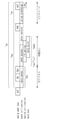
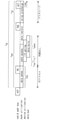
図1は、本発明の実施形態に係るメモリモジュール100とメモリ装置120とを示す概略図である。
例えば、メモリモジュール100は、DDR4 SDRAM DIMMのようなデュアルインラインメモリモジュール(DIMM)である。
メモリモジュール100は、ピン相互接続構造を有する印刷回路基板110(以下、PCBと記す)、PCB110に実装されるメモリ装置120(例えば、RAMチップのようなメモリチップ)、及びメモリ装置120と、ワークステーションや個人用コンピュータのマイクロプロセッサのようなメモリモジュール100を使用する電子装置とを接続するためのピン130とを含む。
PCB110は、両面に形成されるピン130とメモリ装置120と、貫通するピン配線構造を含み、メモリ装置120は積層(貫通シリコンビア又はTSVを使用して)され得る。
FIG. 1 is a schematic view showing a
For example, the
The
The
図2A及び図2Bは、各々本発明の実施形態に係る拡張されたアクティブ(又はACT+)命令語を使用するデータ接続動作の例を示す図である。
図2A及び図2Bで、多様なタイミングパラメーター(例えば、tRC、tRAS)を示す。
これらのパラメーターは、関連された部分でより詳細に説明されるが、これらの定義と使用は、JEDEC DDR4 SDRAM標準によって提供され、当業者に広く公知された事項である。
2A and 2B are diagrams showing an example of a data connection operation using the extended active (or ACT +) instruction word according to the embodiment of the present invention, respectively.
2A and 2B show various timing parameters (eg, t RC , t RAS ).
These parameters are described in more detail in the relevant sections, but their definitions and uses are provided by the JEDEC DDR4 SDRAM standard and are widely known to those of skill in the art.
DDR4標準で、CID(チップID、又はランク)のために3つのピンが、バンク(メモリチップ内の行と列の分離されたアレイ)アドレッシングのために4つのピンが、行(そして、列)アドレッシングのためには18個のピンが使用される。
DDR4 SDRAMのアドレスピンは、行と列のアドレッシングのために再使用される。
DDR4標準で、メモリコントローラは互いに異なるサイクルの間に同一のピンに伝達される2つの命令語(ACT(activate)とRD/WR(read/write))を使用してSDRAMアドレスにアクセスする。
In DDR4 standard, 3 pins for CID (chip ID, or rank), 4 pins for bank (row and column separated array in memory chip) addressing, row (and column) Eighteen pins are used for addressing.
DDR4 SDRAM address pins are reused for row and column addressing.
In the DDR4 standard, memory controllers access a SDRAM address using two instructions (ACT (active) and RD / WR (read / write)) transmitted to the same pin during different cycles.
アクティブ命令語(ACT)は、行アドレス(18ピン)を使用して行を活性化させ、活性化された行を行バッファにロードさせる一方、読出し/書込み命令語(RD/WR)は行バッファから対応する列を選択するために列アドレス(10ピン)を使用する。
ここで、“RD/WR”は読出し命令語(Read command)と書込み命令語(Write command(又は他の列アドレス命令語)の縮約された表現であり、これらの2つの命令語の形態又は分類は特定的に言及(例えば、“RD/WR”、“RD”、及び“WR”は読出し又は書込み命令語を示すための同意語として使用される)しない以上区分されなく、使用される。
The active instruction (ACT) uses the row address (pin 18) to activate the row and loads the activated row into the row buffer, while the read / write instruction (RD / WR) is the row buffer. Use the column address (pin 10) to select the corresponding column from.
Here, "RD / WR" is an abbreviated expression of a read command word (Read command) and a write command word (Write command (or another column address command word), and the forms of these two command words or Classification is used without distinction as long as it is not specifically mentioned (eg, "RD / WR", "RD", and "WR" are used as synonyms to indicate a read or write command).
DDR4標準で、現在のピン使用及びアドレッシング方式は高容量メモリを支援しない。
例えば、現在のDDR4標準は、DRAMチップ当たり2GB容量であり、ランク当たり(同時にアドレッシング可能な)16DRAMチップ(例えば、各々のDRAMチップはランク内で1回に総16×4=64ビットのデータアクセスのために4ビットデータを提供する)、及び8個ランク(又は積層可能であるDRAMチップのセット)のようなチップ構成を仮定すれば、DIMM当たり256GBのみを支援することができる。
With DDR4 standard, current pin usage and addressing schemes do not support high capacity memory.
For example, the current DDR4 standard is 2GB capacity per DRAM chip and 16 DRAM chips per rank (which can be attached at the same time) (eg, each DRAM chip has a total of 16 x 4 = 64 bits of data access at a time within the rank). (Providing 4-bit data for), and assuming chip configurations such as 8 ranks (or a set of stackable DRAM chips), only 256 GB per DIMM can be supported.
しかし、この容量はこのような厳格な設定条件のみで得られる。多くの場合、アーキテクチャによって規定された(意図された)行と列の数と基底のハードウェアで支援される実際の行と列の数の間には不均衡が存在し(例えば、アーキテクチャの効率的な具現のために設計されたことより過度に多い数の行と過度に少ない数の列がハードウェアに存在するか、又は逆に、過度に少ない行と過度に多い数の列が存在する場合)、これは必然的にピンの消耗を引き起こす。
全体の容量の増加や不均一な行/列の数を許容するために1つの解決策はさらに多いピンを追加することである。
しかし、このような解決策は費用を過度に必要とし、現在のDDR4標準の変更を必要とする。
However, this capacity can be obtained only under such strict setting conditions. Often there is an imbalance between the number of rows and columns specified by the architecture (intended) and the actual number of rows and columns supported by the underlying hardware (eg, the efficiency of the architecture). There are too many rows and too few columns in the hardware than designed for realization, or conversely, there are too few rows and too many columns. If), this inevitably causes pin wear.
One solution is to add more pins to allow for an increase in overall capacity and a non-uniform number of rows / columns.
However, such a solution is excessively costly and requires changes to the current DDR4 standard.
本発明の実施形態によれば、図2Bに示すように、1つの可能な解決策は2サイクルのアクティブ(ACT)命令語(通常の1サイクルアクティブ命令語の代わりに)である、拡張アクティブ命令語(ACT+)を使用することである。
比較として、図2AはDDR4での標準アクティブ命令語(ACT)を示す。
図2Aと図2B(そして、他のタイミング図)で、上方から下方に[(i)メモリ命令語及びアドレスバス、(ii)メモリバンク、(iii)メモリ装置(例えば、DRAMチップ)、及び(iv)メモリデータバス]であるアクセスされる4つの別の水平リソースと共にタイミング(時間)は左側から右側に進行する。
要約すれば、メモリモジュール(DIMMのような)上にランクを構成するメモリ(DRAM)チップのセットはバンク単位(メモリチップ内での論理的区分)にアクセスされ、各々のバンクは行で構成され、そして各々の行は複数の列で構成される。
According to an embodiment of the invention, as shown in FIG. 2B, one possible solution is an extended active instruction, which is a two-cycle active (ACT) instruction (instead of the usual one-cycle active instruction). To use the word (ACT +).
For comparison, FIG. 2A shows the standard active instruction word (ACT) in DDR4.
In FIGS. 2A and 2B (and other timing diagrams), from top to bottom [(i) memory commands and address buses, (ii) memory banks, (iii) memory devices (eg DRAM chips), and ( The timing (time) progresses from left to right with four other horizontal resources being accessed: iv) memory data bus.
In summary, a set of memory (DRAM) chips that make up a rank on a memory module (like a DIMM) is accessed on a bank-by-bank basis (logical division within the memory chip), and each bank is made up of rows. , And each row consists of multiple columns.
各々のDIMMはランクやDRAMチップのセットを複数に含む。
説明を簡単にするために、DIMMにアクセスする時、1つのランク内に1つのシングルバンクのみを含む単一ランク構成のみを考慮する。
アクティブ命令語(ACT)は、バンク(例えば、3又は4ビット)とバンク内の行(例えば、18ビットまで)を指定することができる。
図2Aと図2Bで左側から右側の時間軸に沿って行が先にアクセスされ(ACT命令語によって指定される)、列(RDのような読出し/書込み(RD/WR)命令語によって指定される)が続いてアクセスされる。
Each DIMM contains multiple sets of ranks and DRAM chips.
For simplicity of explanation, when accessing DIMMs, consider only a single rank configuration containing only one single bank within a rank.
The active instruction word (ACT) can specify a bank (eg, 3 or 4 bits) and a line within the bank (eg, up to 18 bits).
Rows are accessed first along the left-to-right time axis in FIGS. 2A and 2B (specified by the ACT instruction word) and are specified by the column (read / write (RD / WR) instruction word such as RD). Is subsequently accessed.
これは装置当たり4又は8データワード又はDIMM当たり32又は64バイトのデータバースト(Burst)が読み出されるか、或は書き込まれるようにする。
各々の装置の同一の行で4又は8データワード(DIMMで32又は64バイトの連続バイト)の追加的なアクセスは迅速に遂行される。
しかし、他の行へのアクセスのために、プリチャージ命令語(PRE)を使用することができ、後続するアクティブ命令語(ACT)によってアクセスされる次の行の準備のために現在の行が再びメモリアレイ内に書き込まれる。
This allows a data burst of 4 or 8 data words per device or 32 or 64 bytes per DIMM to be read or written.
Additional access to 4 or 8 datawords (32 or 64 bytes of contiguous bytes in DIMMs) on the same row of each device is performed quickly.
However, a precharge instruction word (PRE) can be used for access to other lines, and the current line is prepared for the next line to be accessed by a subsequent active instruction word (ACT). It is written into the memory array again.
図2Bの実施形態で、拡張されたアクティブ命令語(ACT+)が使用される。
ここで、アクティブ命令語(ACT)は1つのクロックサイクルから2つのクロックサイクルに拡張される。
即ち、アクティブ命令語(ACT)は第2クロックサイクル(ACT+)で追加的なアドレスビットを提供することができるので、提供される行アドレスビットの数を増加させることができる。
例えば、DDR4標準で、追加されるクロックサイクル(ACT+)は同一の行アドレスピンを通じて行アドレス(総36ビット)の他の18ビット(拡張ビット)を伝送するのに使用され、これは相変わらず同一(又はそれ以上の)である量のデータをアドレッシングできながらも、はるかに狭い行(即ち、さらに少ない数の列)を許容する。
他の実施形態で、拡張されたアクティブ命令語(ACT+)が適切な演算コード(op code)を有するように10又は12行アドレスビットが拡張されたアクティブ命令語(ACT+)によって提供することができる。
In the embodiment of FIG. 2B, the extended active instruction word (ACT +) is used.
Here, the active instruction word (ACT) is extended from one clock cycle to two clock cycles.
That is, since the active instruction word (ACT) can provide additional address bits in the second clock cycle (ACT +), the number of row address bits provided can be increased.
For example, in the DDR4 standard, the added clock cycle (ACT +) is used to transmit the other 18 bits (extended bits) of the row address (36 bits total) through the same row address pin, which is still the same (extended bits). Allows much narrower rows (ie, a smaller number of columns) while being able to address an amount of data (or more).
In other embodiments, 10 or 12 line address bits can be provided by an extended active instruction (ACT +) such that the extended active instruction (ACT +) has an appropriate opcode. ..
例えば、所定の実施形態で、拡張されたアクティブ命令語(ACT+)を支援するメモリ装置は、標準ACT(単一サイクル)RAC命令語と、又は新しい(2個サイクル)ACT/(ACT+)プロトコルを認識するために初期化時点に設定することができる。
このような方式には、単なる1つのACT命令語のみが存在し、メモリ装置は標準DDR4アーキテクチャによって、発行される単一アクティブ命令語(ACT)を受信するか、又は拡張されたACT(ACT+)プロトコルが使用される場合、連続されるサイクルの間に発行される2回のアクティブ命令語を受信することを予測することができる。
For example, in a given embodiment, a memory device that supports an extended active instruction (ACT +) may use a standard ACT (single cycle) RAC instruction or a new (two cycle) ACT / (ACT +) protocol. It can be set at the time of initialization for recognition.
In such a scheme, there is only one ACT instruction word, and the memory device receives a single active instruction word (ACT) issued by the standard DDR4 architecture, or has an extended ACT (ACT +). When the protocol is used, it can be expected to receive two active instructions issued during a continuous cycle.
各行が単なる1つの4ビットの列を有する極端の場合でも、先に説明した2サイクルの間に36行アドレスビットを有する拡張されたアクティブ命令語(ACT+)を使用すれば、この拡張された行アドレス機能を使用する単一DRAMチップはピン数やピン費用の変更や増加無しでこのような4-ビット列(ニブル又はハーフバイト)の240又はDDR4アーキテクチャ規格の512GBデータ(即ち、4ビットのバンクアドレス及び36ビットの拡張された行アドレスを使用して)にアクセスすることができる。
これはDDR4標準が全体DIMM(128個のDRAMチップまで含む)のために提供することより単一メモリチップで既にさらに大きい容量値である。
Even in the extreme case where each row has only one 4-bit column, this extended row can be used with the extended active instruction (ACT +) which has 36 row address bits during the two cycles described above. A single DRAM chip using the address function can have such 4-bit string (nibble or half byte) 240 or DDR4 architecture standard 512 GB data (ie, 4-bit bank address) without changing or increasing the number of pins or pin costs. And can be accessed using the 36-bit extended row address).
This is already a larger capacity value on a single memory chip than the DDR4 standard provides for total DIMMs (including up to 128 DRAM chips).
所定の実施形態で、さらに狭い行はDDR4DIMMでこのようなアクティブ命令語(ACT+)の拡張のために従来のSDRAMチップを相変化RAM(以下、PRAM)に代替するのに適用することができる。
例えば、PRAMは、4-ビット幅(1024列)に対して512バイトサイズの行を有するDRAMチップを含む比較できるSDRAMチップに比べて狭い行(例えば、少ない数の列)の数を増加させるのに容易である。
拡張されたアクティブ(ACT)命令語の他の実施形態で、アクティブ(ACT)命令語は変更されなく、追加的なアドレッシングビット(10又は12ビット)を伝達するために“ACT+”と称される新しい1サイクルの命令語が単純に後続され得る。
In certain embodiments, a narrower line can be applied in DDR4DIMM to replace a conventional SDRAM chip with a phase change RAM (PRAM) for such an extension of the active instruction word (ACT +).
For example, a PRAM increases the number of narrow rows (eg, a small number of columns) compared to a comparable SDRAM chip that includes a DRAM chip with 512 byte size rows for a 4-bit width (1024 columns). Easy to use.
In another embodiment of the extended active (ACT) instruction, the active (ACT) instruction remains unchanged and is referred to as "ACT +" to convey additional addressing bits (10 or 12 bits). A new one-cycle command word can simply be followed.
例えば、図2Bに示したように、(ACT+)命令語は拡張された行情報を伝達するために第1ACT命令語に直ちに続く(即ち、先に説明した2サイクルの(ACT+)命令語のような方式に動作)。
新しい(ACT+)命令語それ自体は、ACT命令語(DDR4で専用命令語ビットを有する)に比べて著しく多いビット数が要求されるので、標準ACT命令語が1サイクルで2サイクルに長くなる時、使用可能なアドレスビットの長さより残っている可用アドレスビットの数は若干減少(18ビットの代わりに10又は12ビット)することができる。
For example, as shown in FIG. 2B, the (ACT +) command immediately follows the first ACT command (ie, like the two-cycle (ACT +) command described above to convey extended row information. Works in various ways).
When the standard ACT instruction is lengthened to 2 cycles in 1 cycle, the new (ACT +) instruction itself requires a significantly higher number of bits than the ACT instruction (which has dedicated instruction bits in DDR4). , The number of available address bits remaining can be slightly reduced (10 or 12 bits instead of 18 bits) from the length of the available address bits.
図3は本発明の実施形態に係る拡張された読出し(RD+)命令語を使用したデータアクセス動作の例を示す図である。
図3に示すような他の実施形態で、読出し/書込み(RD/WR)命令語(又は他の列アドレス命令語)は先に説明した追加された列情報を伝達するためのACT命令語に対する変更方式と同一の方式に変更することができる。
例えば、DRAMサイズは、ピン費用やピン数の増加無しで追加的なアドレッシングビット(10又は12のさらに多い列アドレスビット)を指定するためのRD/(WR+)命令語を使用することによって列サイズが10列アドレスビットで20又は22列アドレスビットに増加する方式に増加することができる。
FIG. 3 is a diagram showing an example of a data access operation using the extended read (RD +) instruction word according to the embodiment of the present invention.
In another embodiment as shown in FIG. 3, the read / write (RD / WR) instruction (or other column address instruction) is for the ACT instruction for transmitting the added column information described above. It can be changed to the same method as the change method.
For example, the DRAM size is column size by using the RD / (WR +) instruction to specify additional addressing bits (10 or 12 more column address bits) without pin cost or increase in pin count. Can be increased in a manner that increases from 10 column address bits to 20 or 22 column address bits.
上述した技術の中でいずれか1つ(又は2つの技術の組み合わせ)はピン費用やピン数の変更無しでメモリチップのアドレス機能(即ち、TBサイズやそれ以上に)を画期的に増加させることができる。
(ACT+)又はRD/(WR+)の特別な具現は、DIMMの固定された機能である必要はない。
例えば、所定の実施形態では、拡張されたACT命令語又は拡張されたRD/WR命令語を使用するためのシステムの選択は初期化動作(そして、後続される初期化動作で変更可能な)で実行することができる。
One of the techniques described above (or a combination of the two techniques) dramatically increases the addressing capabilities of the memory chip (ie, TB size and above) without changing pin costs or pin counts. be able to.
The special embodiment of (ACT +) or RD / (WR +) does not have to be a fixed function of the DIMM.
For example, in certain embodiments, the choice of system for using the extended ACT or extended RD / WR instructions is in the initialization operation (and can be changed in subsequent initialization operations). Can be executed.
図4A及び図4Bは、各々本発明の実施形態に係るバックツーバック(back to back)RAS/CAS命令語シークェンスを使用するデータアクセス動作の例を示す図である。
ここで使用するように、RASは“行アドレスストロボ”、CASは“列アドレスストロボ”の本来の意味を有するが、これらの用語の各々はメモリチップの読出し又は書込み動作で行アドレスと列アドレスを提供する意味として大部分使用される。
追加的なアドレスビットを提供するための二重CAS(即ち、バックツーバックCAS)シークェンスの例としては、後述する説明及び図6を参照すればよい。
4A and 4B are diagrams showing an example of a data access operation using a back-to-back RAS / CAS command word sequence according to an embodiment of the present invention, respectively.
As used here, RAS has the original meaning of "row address strobe" and CAS has the original meaning of "column address strobe", but each of these terms refers to the row address and column address in the read or write operation of the memory chip. Mostly used as a meaning to provide.
See below and FIG. 6 for examples of double CAS (ie, back-to-back CAS) sequences to provide additional address bits.
図4A、4Bは、本発明の実施形態に係る追加的な行/列情報を提供するための追加的な技術、即ち新しいバックツーバックRAS/CASシステムを使用する例を示す。
このメカニズムで、非使用アドレスビット(列又は行)が拡張されたアドレス情報を伝達し、標準読出し/書込み(RD/WR)命令語より先に命令語が提供される新しいRD/WRCASが定義される。
一例として、DDR4で、行アドレスビットの中の3個上位-ビットが読出し(RD)及び書込み(WR)命令のためにCASビットと共に使用可能である。
他の実施形態で、基底のメモリ装置は10個列アドレスビットが提供することより少ない列を支援し、したがってこれら余分の列アドレスビットは拡張された行アドレスビットを伝達するのに再割り当てすることができる。
4A and 4B show an example of using an additional technique for providing additional row / column information according to an embodiment of the invention, ie, a new back-to-back RAS / CAS system.
This mechanism defines a new RD / WRCAS in which unused address bits (columns or rows) carry extended address information and the instructions are provided before the standard read / write (RD / WR) instructions. To.
As an example, in DDR4, the three most significant bits of the row address bits can be used with the CAS bits for read (RD) and write (WR) instructions.
In another embodiment, the underlying memory device supports fewer columns than the 10 column address bits provide, so these extra column address bits are reassigned to carry the extended row address bits. Can be done.
他の実施形態で、列アドレス命令語で動的に選択可能な特徴(オンザフライ(on-the-fly)データバースト長さのような)を制御するために提供される上位行アドレスビットが追加的な拡張されたアドレスビット及び静的設定にデフォルトされた(defaulted to)特定な動的特徴として用途変更することができる。
これらの列アドレスの変更と共に、読出し/書込み(RD/WR)命令語の用途変更を支援するために新しいタイミングパラメーターと変更されたアクティブ(ACT)及び読出し/書込み(RD/WR)タイミングが提供される。
このような特徴は、標準読出し/書込み(RD/WR)プロトコル(RD/WRインストラクションはRDで表現される)を示した図4A、及び変更されたRAS/CAS命令語シークェンスを示した図4Bに説明される。
In other embodiments, additional high row address bits are provided to control dynamically selectable features (such as on-the-fly data burst length) with column address instructions. It can be repurposed as a specific dynamic feature that is defaulted to a wide range of extended address bits and static settings.
Along with these column address changes, new timing parameters and changed active (ACT) and read / write (RD / WR) timings are provided to assist in changing the use of read / write (RD / WR) instructions. To.
Such features are shown in FIG. 4A showing the standard read / write (RD / WR) protocol (RD / WR instructions are represented by RD) and FIG. 4B showing the modified RAS / CAS instruction word sequence. Be explained.
さらに詳細には、図4Aに示した標準DDR4で、後続される読出し/書込み(RD/WR)命令語は列アドレス(CAS、10ビット)を提供する一方、アクティブ(ACT)命令語は行アドレス(RAS、18ビット)を提供する。
4個までのバンクビットと共に提供されるこれら28(18+10)ビットはランクへの特定(64ビット)読出し又は書込みアクセスのためにランクを構成する各々のDRAMチップ(例えば、4、8、或いは16メモリチップデータ幅(例えば、4、8、或いは16ビット)をアドレッシングする。
More specifically, in the standard DDR4 shown in FIG. 4A, the subsequent read / write (RD / WR) instruction provides the column address (CAS, 10 bits), while the active (ACT) instruction is the row address. (RAS, 18 bits) is provided.
Provided with up to four bank bits, these 28 (18 + 10) bits are each DRAM chip (eg, 4, 8, or 16 memory) that constitutes a rank for specific (64-bit) read or write access to the rank. Address the chip data width (eg, 4, 8, or 16 bits).
しかし、RASとCASをバックツーバック方式に伝達することによって、任意の非使用アドレスビット(例えば、RD又はWRのようなCAS命令語の3つの非使用行アドレスビット共に提供されるRASとCASのためのビット)は、DDR4で定義されたことと異なる行及び列配列を有するメモリチップを最大に活用する場合のような異なるフォーマット又は分類にアドレッシングする拡張された行や列を提供するために再設定することができる。
加えて、拡張された行アドレスのために、メモリ装置はアクティブ(ACT)命令語(例えば、データアクセスの遅延を避けるために利用可能である18行アドレスビットと共に)によって指定されたすべての行に初期にアクセスするように設定され、(できる限り直ちに)後続する読出し命令語(RD)に残余(拡張された)行アドレスビットを使用して選択を減少させる。
However, by transmitting RAS and CAS back-to-back, any unused address bits (eg, RAS and CAS provided with the three unused row address bits of a CAS instruction such as RD or WR). Bits for) are re-arranged to provide extended rows and columns to address different formats or classifications, such as when making full use of memory chips with different rows and column arrays as defined in DDR4. Can be set.
In addition, due to the extended row address, the memory device is on every row specified by the active (ACT) instruction word (eg, with the 18 row address bits available to avoid delays in data access). It is set to be initially accessed and uses the remaining (extended) row address bits in the subsequent read instruction (RD) (as soon as possible) to reduce the selection.
例えば、メモリ装置は、最初提供される18行アドレスビットによってアドレッシングできるすべての行のための行バッファを含む。
他の実施形態で、メモリ装置は、すべてのこのような行を1つの行バッファにロードすることを開始するが、行アドレスの余りが一旦提供されれば、実際の行が行バッファにロードされるようにただ許諾することができる。
例えば、バックツーバックRAS/CAS命令語シークェンスでアドレッシングのために利用可能である31ビット(18RAS+10CAS+3非使用)を使用して、18ビットの拡張された行アドレスがACT命令語に提供され、3ビット(8個列)の列アドレスと共に直ちに後続されるRD/WR命令語に残る10ビットの拡張された行アドレスの提供が続く。
For example, the memory device contains a row buffer for all rows that can be addressed by the initially provided 18 row address bits.
In another embodiment, the memory device initiates loading all such rows into one row buffer, but once the remainder of the row address is provided, the actual rows are loaded into the row buffer. Can just be licensed.
For example, using 31 bits (18RAS + 10CAS + 3 not used) available for addressing in the back-to-back RAS / CAS instruction sequence, an 18-bit extended row address is provided for the ACT instruction and 3 bits. The provision of the 10-bit extended row address that remains in the RD / WR instruction immediately following with the (8 columns) column address follows.
したがって、何らかのピン数の増加無しでも総アドレス性能は8倍増加し、基本的な行と列のサイズが基本メモリチップ技術(PRAMのような)に最適化されるように調整され得る。
他の実施形態で、CAS(可能には非使用アドレスビットの一部によって拡張された)が列アドレスと共に拡張された行アドレスの余りを伝達する一方、RASは単なる行アドレスの一部を伝達することができる(又は逆に拡張された列アドレスに対して他の実施形態で具現することができる)。
この命令語シークェンスの変更は、メモリモジュールにアクセスするためにメモリコントローラによって使用されるタイミングパラメーターの調整を要求することができる。
Therefore, the total address performance can be increased by a factor of 8 without any increase in the number of pins, and the basic row and column sizes can be adjusted to be optimized for basic memory chip technology (such as PRAM).
In other embodiments, CAS (possibly extended by some of the unused address bits) conveys the remainder of the extended row address along with the column address, while RAS conveys only part of the row address. Can (or vice versa can be embodied in other embodiments for extended column addresses).
This instruction sequence change can require adjustment of the timing parameters used by the memory controller to access the memory module.
例えば、DDR4で、tRCDとtCLが影響を受ける。
ここで、tRCD(RASとCASとの間の遅延)はアクティブ(ACT)命令語と後続する最初読出し(RD)又は書込み(WR)命令語が提供される時間の最小時間(即ち、クロックサイクル)を意味する(即ち、ACT命令語の開始(又は終了)から対応するRD/WR命令語の開始(又は終了)まで測定される時間)。
その上に、tCL(又はtCAS、CASレイテンシと公知される)は、CASの供給時点とデータバス上で最初列に対応するデータアクセスが可能な時点との間の時間を意味する。
図4BでtRCD+tCLに対応する全体時間が図4Aの対応する時間と同一である(即ち、tRCDの減少量がtCLの増加量と同一)。
For example, in DDR4, t RCD and t CL are affected.
Here, t RCD (delay between RAS and CAS) is the minimum time (ie, clock cycle) in which the active (ACT) instruction and the subsequent first read (RD) or write (WR) instruction are provided. ) (Ie, the time measured from the start (or end) of the ACT command word to the start (or end) of the corresponding RD / WR command word).
In addition, t CL (or t CAS , also known as CAS latency) means the time between the point of supply of CAS and the time of data access corresponding to the first column on the data bus.
In FIG. 4B, the total time corresponding to t RCD + t CL is the same as the corresponding time in FIG. 4A (that is, the amount of decrease in t RCD is the same as the amount of increase in t CL ).
図4Bで、さらに長いtCL時間にしたがう性能イッシューを避けることを助けるために、幾つかの実施形態ではオープンページ(オープン行)方策と共に新しいタイミングパラメーターtCL_L(long)とtCL_S(Short)とが定義される。
ここで、tCL_L(例えば、図4BのtCLと示した)がページ内で列に最初アクセスするためにtRCDと共に使用され、tCL_Sはオープンページで後続の行バッファ(同一行の他の列)アクセスのために使用することができる。
これは長短の相違点(例えば、tRRD_LとtRRD_S)を有するDDR4に既に存在する一部のタイミングパラメーターと似ているか、又は同様であり、メモリコントローラはいつtCL_LとtCL_Sを使用するかを追跡することができる。
このような技術の具現には追加的な命令語が必要としなく、メモリ構成は他のtCLを認知する必要がない。
In Figure 4B, to help avoid performance issues that follow longer tCL times, in some embodiments with new timing parameters tCL_L (long) and tCL_S (Short) along with an open page (open line) strategy . Is defined.
Here, t CL_L (eg, shown as t CL in FIG. 4B) is used with t RCD to first access the column in the page, and t CL_S is the open page and the subsequent row buffer (other in the same row). Column) Can be used for access.
This is similar to or similar to some timing parameters already present in DDR4 with long and short differences (eg, t RRD_L and t RRD_S ), and when the memory controller uses t CL_L and t CL_S . Can be tracked.
The realization of such a technique does not require additional instructions and the memory configuration does not need to recognize other tCLs .
図5は、本発明の実施形態に係るバックツーバックCAS/CAS(二重CAS)命令語シークェンスを使用するデータアクセス動作の例を示す図である。
図5で、2つのCAS命令語(例えば、バックツーバックCAS又は二重CAS命令語、2つのRD命令語(RDとRD+)に示した)がアドレスの拡張のために使用することができる。
FIG. 5 is a diagram showing an example of a data access operation using the back-to-back CAS / CAS (double CAS) instruction word sequence according to the embodiment of the present invention.
In FIG. 5, two CAS instructions (eg, shown in back-to-back CAS or double CAS instructions, two RD instructions (RD and RD +)) can be used for address expansion.
例えば、1つ又は2つのCAS命令語は、追加(拡張)アドレスビットを提供することができる。
アドレスビットの割り当ては、基本メモリ装置に基づいて設定することができ、メモリ装置の特性を活用するときのためにアドレスビットを2つのCAS命令語の中でさらに適切なところに移動するように割り当てることができる。
例えば、メモリ装置が単一CAS命令語によってアドレッシングされることよりさらに多い列を有する大きい行を支援する場合、追加的な列アドレスビットは“論理行”アドレス拡張として機能するように第1CAS命令語に提供されるが、“論理行”アドレス拡張は大きい行の各々を多いさらに小さい行に効率的に分割し、さらに小さい行の各々は標準アーキテクチャで最も大きい可能な行サイズである。
第2CAS命令語は、以後、標準CAS命令語と同様に機能することができる。
For example, one or two CAS instructions can provide additional (extended) address bits.
Address bit assignments can be set based on the basic memory device and assign the address bits to move to the more appropriate place in the two CAS directives for when taking advantage of the characteristics of the memory device. be able to.
For example, if the memory device supports a large row with more columns than it is addressed by a single CAS instruction, the additional column address bits should act as a "logical row" address extension for the first CAS instruction. As provided in, the "logical row" address extension efficiently divides each of the larger rows into many smaller rows, and each of the smaller rows is the largest possible row size in the standard architecture.
The second CAS command can subsequently function in the same manner as the standard CAS command.
その他の例をあげれば、メモリ装置が大きい数の小さい行を支援する場合(即ち、アドレス可能なことよりさらに多い行)、第1CAS命令語は、最初のRAS命令語にマッチングする各々の可能な対応行アドレスのための分離された行バッファと共に、行内で特定列を選択するための標準CAS命令語である。
第2CAS命令語は、以後のどの行バッファが実際にデータを供給(又は受信)するかを選択するための行バッファ選択に使用される。
他の実施形態で、増加されたアドレッシング機能を使用するために拡張されたアドレスビットは、他の論理方式(例えば、二重CAS命令語内で再分配)で整列させることができる。
As another example, if the memory device supports a large number of small rows (ie, more rows than can be addressed), the first CAS instruction is each possible to match the first RAS instruction. A standard CAS instruction for selecting a particular column within a row, along with a separate row buffer for the corresponding row address.
The second CAS instruction word is used for row buffer selection for selecting which subsequent row buffer actually supplies (or receives) data.
In other embodiments, the address bits extended to use the increased addressing function can be aligned in other logical schemes (eg, redistributed within the dual CAS command word).
図6は、本発明の実施形態に係るバックツーバックRAS/CAS又はCAS/CAS命令語シークェンスを使用するデータアクセス動作の例を示す図である。
ここで、2つのCAS命令語(例えば、バックツーバックCAS又は二重CAS命令語、例として、2つのRD命令語として示したように)が図4Bの実施形態でさらにアドレスを拡張するために使用することができる。
図6で第2RD命令語は、(RD+)命令語として示している。
先に説明した図2Bの(ACT+)命令語と同様に、余分の命令語が余分のアドレスビットを提供するために使用され、したがって10又は12ビットのアドレスビットの追加が可能である。また、これは以前の技術と組み合わせることができる。
FIG. 6 is a diagram showing an example of a data access operation using the back-to-back RAS / CAS or CAS / CAS command word sequence according to the embodiment of the present invention.
Here, in order for two CAS commands (eg, back-to-back CAS or double CAS commands, eg, as shown as two RD commands) to further extend the address in the embodiment of FIG. 4B. Can be used.
In FIG. 6, the second RD command word is shown as a (RD +) command word.
Similar to the (ACT +) command word of FIG. 2B described above, the extra command word is used to provide the extra address bits, so it is possible to add 10 or 12 bit address bits. It can also be combined with previous technology.
限定されない例として、拡張された行アドレスの残余行アドレスビットを提供するための第1RD命令語と共に、(RD+)命令語が列アドレスを提供するために使用することができる。
他の実施形態で、最初列アドレスビットが第1RD命令語と共に提供され、(RD+)命令語は拡張された列アドレスの残余アドレスビットを提供するために使用することができる。
他の実施形態で、(RD+)命令語(又は、第2RD命令語)が列アドレスの全て或いは一部を提供するための一般列アクセス時間まで遅延されるのに反して、第1RD命令語はACT命令語に直ちに続く(例えば、余分の行アドレスビットと可能には一部の列アドレスビットをバックツーバックRAS/CASシークェンスの一部に提供)。
As a non-limiting example, the (RD +) instruction can be used to provide a column address, along with a first RD instruction to provide the residual row address bits of the extended row address.
In other embodiments, the first column address bits are provided with the first RD instruction word, and the (RD +) instruction words can be used to provide the residual address bits of the extended column address.
In other embodiments, the first RD instruction is delayed until the general column access time for the (RD +) instruction (or the second RD instruction) to provide all or part of the column address. Immediately following the ACT instruction (eg, providing extra row address bits and possibly some column address bits as part of the back-to-back RAS / CAS sequence).
他の実施形態で、アドレスビット(列アドレスビットのような)は基本的なハードウェアを適切に収容するために2つのCAS(RD又はWRのような)命令語の間で再分配することができる。
例えば、(拡張された)列アドレスが単一命令語に収容されない同一の(広い)行への連続的なアクセスは、それらの拡張された列アドレスが連続されるRD又はWRCAS命令語の対にわたって分離されるようにすることができる。
図6では隣接するACT、RD、及び(RD+)命令語を示しているが、実施形態に係って隣接する命令語の間には(例えば、ACT命令語とRD命令語との間又はRD命令語と(RD+)命令語との間)遅延又はギャップが存在することができる。
In other embodiments, address bits (such as column address bits) may be redistributed between two CAS (such as RD or WR) directives to properly accommodate the basic hardware. can.
For example, continuous access to the same (wide) row where the (extended) column address is not contained in a single instruction word spans a pair of RD or WRCAS instructions where those extended column addresses are contiguous. Can be separated.
Although the adjacent ACT, RD, and (RD +) command words are shown in FIG. 6, between the adjacent command words according to the embodiment (for example, between the ACT command word and the RD command word or RD). There can be a delay or gap (between the command word and the (RD +) command word).
図7は、本発明の実施形態に係る例示的な拡張された読出し(RD+)命令語のためのDDR4 SDRAMの真理表である。
図7を参照すれば、(RD+)命令語は2つの命令語サイクルに掛けて伝達されるように計画される。
この実施形態で、(RD+)命令語は初期化時間で設定することができ、第3チップIDビットC2を使用する(例えば、(RD+)はC2=Hで、RDはC2=L)ことによってRD命令語と区分することができる。
FIG. 7 is a truth table of DDR4 SDRAM for an exemplary extended read (RD +) instruction word according to an embodiment of the invention.
With reference to FIG. 7, the (RD +) command word is planned to be transmitted over two command word cycles.
In this embodiment, the (RD +) command word can be set in the initialization time and by using the third chip ID bit C2 (eg, (RD +) is C2 = H and RD is C2 = L). It can be distinguished from the RD command word.
これはメモリチップの積層を単なる4つに制限する一方、他の実施形態で、他のビットが2つの命令語を区分するために使用することができる。
加えて、図7で、オンザフライ(on-the-fly)バーストモードビット(BC_n)が拡張アドレスビット(A12)の定義に用途変更することができる。
このような実施形態は、オンザフライ(on-the-fly)バーストモード選択を不可能にするが、バーストモードは必要な時にモードレジスター設定を通じて相変わらず変更することができ、他の実施形態では他のビットがアドレスを拡張するために使用することができる。
This limits the stacking of memory chips to just four, while in other embodiments the other bits can be used to distinguish between the two instructions.
In addition, in FIG. 7, the on-the-fly burst mode bit (BC_n) can be repurposed to the definition of an extended address bit (A12).
Such embodiments make on-the-fly burst mode selection impossible, but the burst mode can still be changed through mode register settings when needed, and in other embodiments other bits. Can be used to extend the address.
したがって、図7の(RD+)命令語は、一般的な10ビットの列アドレス(CA)、2ビットのバンクグループ(BG)、及び2ビットのバンクアドレス(BA)に加えて4ビットの追加的な拡張されたアドレス(EA)を伝達することができる。
拡張されたアドレス(EA)ビットは、例えばアクティブ命令語ACTによって指定される18ビットの行アドレス(RA)や10ビットの列アドレス(CA)以外の行アドレスや列アドレス情報をさらに指定するのに使用することができる。
Therefore, the (RD +) instruction in FIG. 7 is a 4-bit additional in addition to the general 10-bit column address (CA), 2-bit bank group (BG), and 2-bit bank address (BA). Extended address (EA) can be transmitted.
The extended address (EA) bits further specify row addresses and column address information other than, for example, the 18-bit row address (RA) and 10-bit column address (CA) specified by the active instruction word ACT. Can be used.
加えて、図7の(RD+)命令語は、第1命令語サイクルに直ちに続く第2命令語サイクルを有し、この時間は2ビットの優先順位フィールドと10ビットの読出しIDフィールド(RID)と共に非使用命令語コード(DDR4アーキテクチャでは予備未来フィールド又はRFU)を利用する。
したがって、図7に示した残余3ビットはRFUになる。
優先順位フィールドと読出しIDフィールド(RID)とは、例えば、メモリ装置がDDR4アーキテクチャで定義されたことに追加的な機能又はストレージ(即ち、追加的な行やバッファ)を有する場合、追加的な情報(例えば、追加的なアドレスビットやバッファ選択ビット)を提供することができる。
In addition, the (RD +) command word in FIG. 7 has a second command word cycle immediately following the first command word cycle, this time with a 2-bit priority field and a 10-bit read ID field (RID). Use a non-used imperative code (preliminary future field or RFU in DDR4 architecture).
Therefore, the remaining 3 bits shown in FIG. 7 become RFU.
Priority fields and read ID fields (RIDs) are, for example, additional information if the memory device has additional functionality or storage (ie, additional rows or buffers) defined in the DDR4 architecture. (For example, additional address bits and buffer selection bits) can be provided.
図8は本発明の実施形態に係るメモリチップの行構造を例示的に示す図である。
所定の実施形態で、ピン数やピン費用の増加無しで追加的な行/列情報を提供するための追加技術はマルチ行バッファ構造を採択することができる。
ここで、メモリ装置は追加アドレスインデックスを支援するために新しい内部組織を有し、追加的な情報を伝達するために新しいRD/WRCAS命令語システムを使用することができる(拡張された行アドレスの一部に指定するために使用されないCASビットを用途変更するように)。
FIG. 8 is a diagram schematically showing a row structure of a memory chip according to an embodiment of the present invention.
In certain embodiments, a multi-row buffer structure can be adopted as an additional technique for providing additional row / column information without increasing the number of pins or pin costs.
Here, the memory device has a new internal organization to support the additional address index and can use the new RD / WRCAS instruction system to convey additional information (extended row address). (To change the use of CAS bits that are not used to specify some).
さらに詳細に説明すれば、図8で示すように、単なる1つのバッファ815(行バッファ)と共に提供される比較的“狭いが、高い(即ち、行の数は多いが、相対的に列の数が少ない)”メモリアレイ810は各々が自分のバッファ835(行バッファ)を有する複数のさらに小さいアレイ830を有する同様のアレイ構造820に分割することができる。
ここで、複数の小さいアレイ830の各々は、メモリアレイ810より行の数は少ないが、列の数は同一の“狭くて短い”構造を有する。
例えば、アレイ構造820は、すべての行のアドレッシングが可能(即ち、17又は18ビットのアドレス空間より小さいか、或いは同一)であるアレイ830を含む一方、メモリアレイ810は通常のアドレッシング可能行より多い行(即ち、17又は18ビットのアドレス空間より多い)を有する。
More specifically, as shown in FIG. 8, the relatively "narrow but high (ie, many rows but relatively many columns) provided with just one buffer 815 (row buffer)". The
Here, each of the plurality of
For example, the
所定の実施形態では、行バッファ835のアドレッシング及びアクセスのためにターゲットデータアレイの行アドレスと共にACT命令語が小さいアレイ830の各々に伝達することができる。
アレイ830の各々は、その行からの情報を対応する自身のバッファ835に提供することによって応答する。
次に、列アドレス、アレイIDと共にRD/WR命令語が伝達され、これは図8の最も下方のアレイ830に図に示したようにターゲットアレイ830のバッファにデータを書き込むか、或いは読み出すようにする。
In certain embodiments, the ACT instruction can be propagated to each of the
Each of the
Next, the RD / WR instruction word is transmitted along with the column address and array ID so that the
言い換えれば、拡張された行アドレスは、ACT命令語に下位行アドレスビット(行ID)を提供し、そしてRD/WR命令語と共に上位行アドレスビット(アレイID)を(CASフィールドの非使用部分に、或いは図7に示した(RD+)命令語のEA、又はRIDビットのような他の非使用アドレスビットに)提供するように支援することができる。
このような方式によれば、ピン数やピン費用の増加無しで又はACT命令語の発行から対応する行への最初データアクセスまでの遅延の増加無しで他の技術のメモリチップ(PRAMのような)に画期的に増加された容量を提供することができる。
In other words, the extended row address provides the lower row address bits (row ID) for the ACT instruction and the upper row address bits (array ID) along with the RD / WR instruction (in the unused portion of the CAS field). , Or to other unused address bits such as the EA of the (RD +) opposition shown in FIG. 7, or the RID bit).
According to such a method, a memory chip of another technology (such as PRAM) without an increase in the number of pins or pin cost, or without an increase in the delay from the issuance of the ACT instruction to the first data access to the corresponding row. ) Can provide a breakthrough increased capacity.
その上に、同一のグループの行(例えば、同一の行IDを共有する)の追加的なRD/WR命令語は、追加的なその他のACT命令語無しで、他のアレイID(最初ACT命令語によって対応するバッファに既にロードされた)を特定するための同一の非使用ビット(例えば、EA、RID、非使用CA)を使用することによって達成することができる。 On top of that, additional RD / WR instructions for rows in the same group (eg, sharing the same row ID) are other array IDs (first ACT instructions) without additional other ACT instructions. This can be achieved by using the same unused bits (eg, EA, RID, unused CA) to identify (already loaded into the corresponding buffer by word).
図9は、本発明の実施形態に係る例示的な拡張された書込み(WR+)命令語のためのDDR4 SDRAMの真理表である。
図9を参照すれば、(WR+)命令語は単一サイクル命令語である。
この実施形態で、(WR+)命令語は初期化時間で設定することができ、第3チップIDビットC2を使用すること(例えば、(WR+)はC2=Hで、WRはC2=L)としてWR命令語と区分することができる。
このような特徴は、メモリチップの積層を4個に制限する一方、他の実施形態では、他のビットが2つの命令語を区分するために使用することができる。
FIG. 9 is a truth table of DDR4 SDRAM for an exemplary extended write (WR +) instruction word according to an embodiment of the invention.
Referring to FIG. 9, the (WR +) command word is a single cycle command word.
In this embodiment, the (WR +) command word can be set by the initialization time, and the third chip ID bit C2 is used (for example, (WR +) is C2 = H and WR is C2 = L). It can be distinguished from the WR command word.
Such a feature limits the stacking of memory chips to four, while in other embodiments, other bits can be used to distinguish between the two instructions.
加えて、図9で、オンザフライ(on-the-fly)バーストモードビット(BC_n)が拡張されたアドレスビット(A12)の定義のために用途変更することができる。
このような実施形態は、オンザフライ(on-the-fly)バーストモード選択を不可能にするが、バーストモードは必要の時にモードレジスター設定を通じて相変わらず変更することができ、他の実施形態では他のビットが拡張されたアドレスビットのために使用することができる。
In addition, in FIG. 9, the on-the-fly burst mode bit (BC_n) can be repurposed for the definition of an extended address bit (A12).
Such embodiments make on-the-fly burst mode selection impossible, but the burst mode can still be changed through mode register settings when needed, and in other embodiments other bits. Can be used for extended address bits.
したがって、図9の(WR+)命令語は、一般的な10ビットの列アドレス(CA)、2ビットのバンクグループ(BG)、及び2ビットのバンクアドレス(BA)に加えて4ビットの追加的な拡張されたアドレス(EA)を伝達することができる。
EAビットは、例えばACT命令語によって指定される18ビットの行アドレス(RA)や10ビットの列アドレス(CA)以外の行アドレスや列アドレス情報を追加的に指定するのに使用することができる。
Therefore, the (WR +) instruction in FIG. 9 is a 4-bit additional in addition to the general 10-bit column address (CA), 2-bit bank group (BG), and 2-bit bank address (BA). Extended address (EA) can be transmitted.
The EA bit can be used to additionally specify row address or column address information other than, for example, the 18-bit row address (RA) or 10-bit column address (CA) specified by the ACT instruction word. ..
図10は、本発明の実施形態に係るメモリチップの列構造を例示的に示す図である。
図8のマルチ行バッファ構造のように、図10に示すように、ピン数やピン費用の増加無しで追加的な行/列情報を提供するための追加技術はマルチ列バッファ構造を採択することができる。
ここで、メモリ装置は追加アドレスインデックスを支援するために新しい内部構造を有することができ、余分の情報を伝達するために新しいACT(RAS)命令語システムを使用することができる(拡張された列アドレスの一部を指定するために使用されないRASビットを用途変更するように)。
FIG. 10 is a diagram schematically showing a row structure of a memory chip according to an embodiment of the present invention.
As shown in FIG. 10, as in the multi-row buffer structure of FIG. 8, an additional technique for providing additional row / column information without increasing the number of pins or the pin cost is to adopt the multi-column buffer structure. Can be done.
Here, the memory device can have a new internal structure to assist with the additional address index, and a new ACT (RAS) command word system can be used to convey extra information (extended column). Use RAS bits that are not used to specify part of the address).
さらに詳細に説明すれば、図10で示すように、単なる1つのバッファ1015(行バッファ)と共に提供される比較的“広いが、短い(即ち、行の数は少ないが、相対的に列の数が多い)”メモリアレイ1010は各々が自分のバッファ1035(行バッファ)を有する複数のさらに小さいアレイ1030を有する同様な構造1020に分割することができる。
ここで、複数の小さいアレイ1030の各々は、メモリアレイ1010と行の数は同一であり、列の数はさらに少ない“狭くて短い”構造を有する。
例えば、アレイ構造1010は、一般的にアドレッシング可能(即ち、10ビットより多いアドレス空間を有する)であることより多い列を有するが、アレイ構造1020は各々すべての列のアドレッシングが可能なアレイ1030を含む(即ち、10ビット以下のアドレス空間を有する)。
More specifically, as shown in FIG. 10, a relatively "wide but short (ie, a small number of rows but a relative number of columns) provided with just one buffer 1015 (row buffer). The
Here, each of the plurality of
For example, the
所定の実施形態では、行バッファ1035のアドレッシング及びアクセスのためにターゲットデータアレイの(相対的に小さい)行アドレスと共にACT命令語が小さいアレイ1030の各々に伝達することができる。
小さいアレイ1030の各々は、対応する行バッファ1035にターゲット行を順にロードする。
加えて、アレイ1030内のターゲット列とターゲットアレイ1030(図10の左側から3番目のアレイ1030の同一)を識別するために列アドレス、アレイIDが提供(例えば、1つ又は2つの後続されるCAS命令語や、また場合によっては、アクティブ命令語(ACT)の部分に含まれ、1つ又は2つの後続されるCAS命令語を使用)される。
In certain embodiments, the ACT instruction can be propagated to each of the
Each of the
In addition, a column address, array ID is provided (eg, one or two subsequent) to distinguish between the target column in the
言い換えれば、拡張された列アドレスは、ACT命令語に行アドレスビット(行ID)を提供し、後続されるRD/WR命令語(下位列アドレスビット(列ID)及び上位列アドレスビット(アレイID)を提供することによって、また場合によっては、ACT命令語内の任意の非使用アドレスビットを使用(ACT命令語にアレイIDを提供することの同一)することによって支援することができる。
これは、ピン数やピン費用の増加無しで、又はACT命令語の発行から対応する列への最初データアクセスまでの遅延の増加無しで幾つのメモリチップ(多い数の列を収容する)を使用して容量を画期的に増加させることができる。
これらの技術及び他の技術が適用可能な分野、即ち、オープンページと広い列が組み合わされることによって同一の広い行に(即ち、同一又は異なるアレイIDに)連続的にアクセスすることが追加的なRASディレイの誘発無しでこの通常のCASレイテンシ(tCL)時間内に達成されるよう組み合わせることができる。
In other words, the extended column address provides the row address bit (row ID) for the ACT instruction word, followed by the RD / WR instruction word (lower column address bit (column ID) and upper column address bit (array). It can be assisted by providing an ID) and, in some cases, by using any unused address bit in the ACT instruction (the same as providing an array ID in the ACT instruction).
It uses several memory chips (accommodating a large number of columns) without an increase in the number of pins or pin costs, or without an increase in the delay from the issuance of the ACT instruction to the first data access to the corresponding column. The capacity can be dramatically increased.
Additional areas where these and other technologies are applicable: continuous access to the same wide row (ie, the same or different array IDs) by combining open pages and wide columns. It can be combined to be achieved within this normal CAS latency (tCL) time without inducing a RAS delay.
図11は、本発明の実施形態に係るメモリ装置のアドレッシング方法の例を説明するためのフローチャートである。
ここで、メモリ装置は、特定アーキテクチャ(DDR4 SDRAMのような)を使用してアクセスされ、使用されるアーキテクチャが一般設定で支援(即ち、アドレス可能な)することより多い行や列を有するものとみなされる。
しかし、本発明の実施形態によれば、メモリ装置の行は、拡張された行アドレスやメモリ装置の列は拡張された列アドレスを使用してアクセスされ、これらの拡張された行アドレスや列アドレスは基本アーキテクチャの組み合わされた行アドレスと列アドレス部分(即ち、2以上の連続されるRAS/CAS命令語)に適合する。
FIG. 11 is a flowchart for explaining an example of an addressing method for a memory device according to an embodiment of the present invention.
Here, the memory device is accessed using a particular architecture (such as DDR4 SDRAM) and has more rows and columns than the architecture used supports (ie, addressable) in the general settings. It is regarded.
However, according to an embodiment of the invention, the rows of the memory device are accessed using the extended row addresses and the columns of the memory device are accessed using the extended column addresses, and these extended row addresses and column addresses are used. Fits the combined row and column address parts of the basic architecture (ie, two or more consecutive RAS / CAS directives).
図11を参照すると、まず、S1110段階で、もし行アドレスが過度に多いビット数を有する場合(即ち、メモリ装置が支援するアーキテクチャより多い行を有する場合)、行アドレスビットは第1サブセットと第2サブセットとに分離され、第1サブセットは行アドレス命令語(例えば、ACT)によって特定され、第2サブセットは後続されるアドレス命令語(例えば、(ACT+)又はRD/WR)によって特定される。 Referring to FIG. 11, first, in step S1110, if the row address has an excessively large number of bits (ie, has more rows than the architecture supported by the memory device), the row address bits are the first subset and the first. Separated into two subsets, the first subset is specified by a row address command word (eg, ACT) and the second subset is specified by a subsequent address command word (eg, (ACT +) or RD / WR).
次に、S1120段階で、行アドレス命令語がメモリ装置の行に対する行アクセスの一部又は全部として発行される。
例えば、メモリ装置がアーキテクチャによって支援される行より少ない数の行を有する場合、すべての行アドレスは行アドレス命令語によって特定することができるが、メモリ装置がアーキテクチャによって支援される行より多い数の行を有する場合には行アドレスの一部のみが(即ち、第1サブセット)行アドレス命令語によって特定され、残る行アドレス(即ち、第2サブセット)は後続アドレス命令語によって特定される。
Next, at step S1120, the row address instruction word is issued as part or all of the row access to the row in the memory device.
For example, if the memory device has fewer rows than the architecture-supported rows, then all row addresses can be specified by the row address instruction, but the memory device has more rows than the architecture-supported rows. If it has rows, only part of the row address (ie, the first subset) is specified by the row address command, and the remaining row addresses (ie, the second subset) are specified by the subsequent address command.
同様に、S1130段階で、もし列アドレスが過度に多いビット数を有する場合(即ち、メモリ装置が支援するアーキテクチャより多い列を有する場合)、列アドレスビットは第3サブセットと第4サブセットとに分離され、第4サブセットは列アドレス命令語(例えば、RD/WRやRD/(WR+))によって特定され、第3サブセットは以前アドレス命令語(例えば、ACT、(ACT+)又はRD/WR)によって特定される。 Similarly, at step S1130, if the column address has an excessively large number of bits (ie, has more columns than the memory device supports), the column address bits are separated into a third subset and a fourth subset. The fourth subset is identified by a column address directive (eg, RD / WR or RD / (WR +)) and the third subset is previously identified by an address directive (eg, ACT, (ACT +) or RD / WR). Will be done.
次に、S1140段階で、列アドレス命令語が行に対する列アクセスの一部又は全部として発行する。
例えば、メモリ装置がアーキテクチャによって支援される列より少ない数の列を有する場合、すべての列アドレスは列アドレス命令語によって特定することができるが、メモリ装置がアーキテクチャによって支援される列より多い数の列を有する場合には列アドレスの一部(第4サブセット)のみが列アドレス命令語によって特定され、残る列アドレス(第3サブセット)は以前アドレス命令語によって特定される。
Next, at step S1140, the column address command word is issued as part or all of the column access to the row.
For example, if the memory device has fewer columns than the architecture-supported columns, all column addresses can be specified by the column address instruction, but the memory device has more columns than the architecture-supported columns. If there is a column, only part of the column address (fourth subset) is specified by the column address command, and the remaining column address (third subset) is previously specified by the address command.
もし、メモリ装置で必要である全体アドレスビット(行及び列数が行アドレス命令語(例えば、ACT)と列アドレス命令語(例えば、RD/WR)によって特定される数より大きくない場合、後続アドレス命令語は列アドレス命令語になるか、或いは以前アドレス命令語は行アドレス命令語になる(バックツーバックRAS/CASのように)。
このようにすれば、2つのアドレス命令語(可能には、バックツーバック方式の)としてもメモリ装置のアドレッシングのために十分である。
If the total address bits (number of rows and columns) required by the memory device are not greater than the number specified by the row address instruction (eg, ACT) and the column address instruction (eg, RD / WR), the subsequent address. The command can be a column address command, or a former address command can be a row address command (like back-to-back RAS / CAS).
In this way, two address instructions (possibly back-to-back) are sufficient for addressing the memory device.
一方、メモリ装置で必要である全体アドレスビット(行及び列数が行アドレス命令語と列アドレス命令語によって特定される数より大きい場合、後続アドレス命令語や以前アドレス命令語(例えば、(ACT+)又はRD/WR)は行アドレス命令語と列アドレス命令語との間で発行される。
例えば、後続アドレス命令語と以前アドレス命令語とは同一の命令語であり、そして拡張された行アドレスビットや拡張された列アドレスビット、また場合によっては、これらの全てを特定することができる。
この後続アドレス命令語は、また行アドレス命令語を直ちに続くか(例えば、(ACT+)又はバックツーバックRAS/CASでのように)、列アドレス命令語の直前に直ちに発行することができる(例えば、バックツーバックCAS/CASでのように)。
On the other hand, the total address bits required by the memory device (if the number of rows and columns is greater than the number specified by the row address command and the column address command, the subsequent address command or the previous address command (eg, (ACT +)). Or RD / WR) is issued between the row address command word and the column address command word.
For example, a subsequent address command and a previous address command are the same command, and extended row address bits, extended column address bits, and, in some cases, all of them can be specified.
This subsequent address command can also be immediately followed by the row address command (eg (ACT +) or back-to-back RAS / CAS) or issued immediately before the column address command (eg,). , Like in back-to-back CAS / CAS).
整理すれば、本発明は、SDRAMライクアーキテクチャの新しい命令語及びタイミング定義を提供するためのものであり、現在のSDRAMアーキテクチャに比べてさらに良いアドレス性能を可能にする。
例えば、幾つかの実施形態では、現在のSDRAMアーキテクチャに比べてさらに良いアドレス性能を可能にするための新しいメモリ構造とアドレス定義を提供することができる。
加えて、他の実施形態では、設定可能なアドレス拡張方法(例えば、メモリチップの初期化やパワーオンの時に活性化される)を提供することができる。
これらの実施形態はピン数やピン費用の増加無しで高容量メモリを支援することができる。これらの実施形態はまたアドレスピンの再利用率を高くすることができる。
In summary, the present invention is intended to provide new instruction words and timing definitions for SDRAM-like architectures, enabling even better address performance compared to current SDRAM architectures.
For example, in some embodiments, new memory structures and address definitions can be provided to enable even better address performance compared to current SDRAM architectures.
In addition, other embodiments can provide configurable address extension methods (eg, activated at memory chip initialization or power-on).
These embodiments can support high capacity memory without increasing the number of pins or the cost of pins. These embodiments can also increase the reuse rate of address pins.
尚、本発明は、上述の実施形態に限られるものではない。本発明の技術的範囲から逸脱しない範囲内で多様に変更実施することが可能である。 The present invention is not limited to the above-described embodiment. Various changes can be made without departing from the technical scope of the present invention.
100 メモリモジュール
110 印刷回路基板(PCB)
120 メモリ装置
130 ピン
100
120
Claims (28)
前記第1の数が前記第2の数より大きく、かつ、前記第1の数が前記第3の数より大きく、かつ、前記第2の数と前記第4の数が同じ場合、
前記第1の数の行アドレスビットを行アドレスビットの第1サブセットと行アドレスビットの第2サブセットとに分離し、前記第1サブセットを前記行アドレス命令語で特定し、前記第2サブセットを後続(next)アドレス命令語で特定する段階と、
前記メモリ装置の行に対する行アクセスの一部又は全部として前記行アドレス命令語を発行する段階と、
前記行アドレス命令語の発行後、前記後続アドレス命令語を発行する段階と、を有し、
前記第2の数が前記第1の数より大きく、かつ、前記第2の数が前記第4の数より大きく、かつ、前記第1の数と前記第3の数が同じ場合、
前記第2の数の列アドレスビットを列アドレスビットの第3サブセットと列アドレスビットの第4サブセットとに分離し、前記第4サブセットは、前記列アドレス命令語で特定し、前記第3サブセットを以前(previous)アドレス命令語で特定する段階と、
前記列に対する列アクセスの一部又は全部として前記列アドレス命令語を発行する段階と、
前記列アドレス命令語の発行前に、前記以前アドレス命令語を発行する段階と、を有し、
前記後続アドレス命令語は、前記第4の数の列アドレスビットを特定する前記列アドレス命令語であり、前記以前アドレス命令語は、前記第3の数の行アドレスビットを特定する前記行アドレス命令語であり、
前記列アドレス命令語を発行する段階は、前記行アドレス命令語を発行する段階の直後に行われ、
前記後続アドレス命令語の発行は前記行アドレス命令語の発行の直後に実行され、
前記以前アドレス命令語の発行は前記列アドレス命令語の発行の直前に実行されることを特徴とするメモリ装置のデータアドレッシング方法。 The data in the memory device is arranged in an array of rows and columns indexed by the first number of row address bits and the second number of column address bits, respectively, and the data is the third number of row addresses. The memory device said to be addressed using an architecture defined by a row address instruction that identifies a bit and a column address instruction that identifies a fourth number of column address bits following the row address instruction. In the data addressing method
When the first number is larger than the second number, the first number is larger than the third number, and the second number and the fourth number are the same.
The first number of row address bits is separated into a first subset of row address bits and a second subset of row address bits, the first subset is specified by the row address instruction term, and the second subset is followed. (Next) The stage of specifying by the address command word,
At the stage of issuing the row address command word as part or all of the row access to the row of the memory device,
After issuing the line address command word, it has a stage of issuing the subsequent address command word.
When the second number is larger than the first number, the second number is larger than the fourth number, and the first number and the third number are the same.
The second number of column address bits is separated into a third subset of column address bits and a fourth subset of column address bits, the fourth subset is specified by the column address command term, and the third subset is specified. The stage of specifying with the previous (previous) address command word,
At the stage of issuing the column address command as part or all of the column access to the column,
It has a stage of issuing the previous address command word before the issuance of the column address command word.
The subsequent address instruction word is the column address instruction word that specifies the fourth number of column address bits, and the previous address instruction word is the row address instruction that specifies the third number of row address bits. Is a word
The step of issuing the column address command word is performed immediately after the step of issuing the row address command word.
The issuance of the subsequent address command word is executed immediately after the issuance of the line address command word.
A method for data addressing of a memory device, characterized in that the issuance of the previous address command word is executed immediately before the issuance of the column address command word.
前記アーキテクチャは、前記列アドレス命令語とデータバスへのデータアクセス可能時点との間の遅延を示す第1アクセス時間によって定義され、
前記第1アクセス時間より長い第2アクセス時間内に前記行のイニシャル(initial)列アクセスを実行する段階と、
前記第1アクセス時間内に前記行への後続(subsequent)列アクセスを実行する段階と、をさらに有することを特徴とする請求項1に記載のメモリ装置のデータアドレッシング方法。 When the first number is larger than the second number, the first number is larger than the third number, and the second number and the fourth number are the same.
The architecture is defined by a first access time that indicates the delay between the column address instruction and the point in time when data is accessible to the data bus.
The stage of executing the initial column access of the row within the second access time longer than the first access time, and
The data addressing method for a memory device according to claim 1, further comprising a step of performing subsequent column access to the row within the first access time.
前記第2の数の列アドレスビットを前記列アドレスビットの第3サブセットと列アドレスビットの第4サブセットとに分離し、前記第4サブセットを前記列アドレス命令語で特定し、前記第3サブセットを以前アドレス命令語で特定する段階をさらに有することを特徴とする請求項1に記載のメモリ装置のデータアドレッシング方法。 When the first number is larger than the second number, the first number is larger than the third number, and the second number and the fourth number are the same.
The second number of column address bits is separated into a third subset of the column address bits and a fourth subset of the column address bits, the fourth subset is specified by the column address instruction term, and the third subset is specified. The data addressing method for a memory device according to claim 1, further comprising a step previously specified by an address instruction term.
前記データは、複数の行と列を有する複数のサブアレイに配列され、各々の前記サブアレイは、行と列のサブセットになり、各々前記第3の数の行アドレスビットと前記第2の数の列アドレスビットとによってインデックスされ、前記行アドレスビットの前記第1サブセットは、前記行アドレスビットの前記第3の数になり、
前記メモリ装置は、前記サブアレイごとに行バッファを含み、
前記サブアレイの各々において、前記行アドレス命令語に応答して対応する前記行アドレスビットの前記第1サブセットによって特定されるサブアレイからの行データを対応する行バッファにロード(load)する段階をさらに有することを特徴とする請求項1に記載のメモリ装置のデータアドレッシング方法。 When the first number is larger than the second number, the first number is larger than the third number, and the second number and the fourth number are the same.
The data is arranged in a plurality of sub-arrays having a plurality of rows and columns, and each of the sub-arrays becomes a subset of rows and columns, the third number of row address bits and the second number of columns, respectively. Indexed by the address bits, the first subset of the row address bits becomes the third number of the row address bits.
The memory device includes a row buffer for each subarray.
Each of the sub-arrays further comprises a step of loading row data from the sub-array identified by the first subset of the corresponding row address bits in response to the row address instruction word into the corresponding row buffer. The data addressing method for a memory device according to claim 1.
前記データは、複数の行と列を有する複数のサブアレイに配列され、各々の前記サブアレイは、行と列のサブセットになり、各々の前記第1の数の行アドレスビットと前記第4の数の列アドレスビットによってインデックスされ、前記列アドレスビットの前記第4サブセットは、前記列アドレスビットの前記第4の数になり、
前記メモリ装置は、前記サブアレイごとに行バッファを含み、
前記サブアレイ各々において、前記行アドレス命令語に応答して対応する前記第1の数の行アドレスビットによって特定されるサブアレイからの行データを対応する行バッファにロードする段階をさらに有することを特徴とする請求項1に記載のメモリ装置のデータアドレッシング方法。 When the second number is larger than the first number, the second number is larger than the fourth number, and the first number and the third number are the same.
The data is arranged in a plurality of sub-arrays having a plurality of rows and columns, and each of the sub-arrays becomes a subset of rows and columns of the first number of row address bits and the fourth number of each. Indexed by the column address bits, the fourth subset of the column address bits becomes the fourth number of the column address bits.
The memory device includes a row buffer for each subarray.
Each of the sub-arrays further comprises loading the row data from the sub-array identified by the corresponding first number of row address bits in response to the row address instruction into the corresponding row buffer. The data addressing method for the memory device according to claim 1.
各々、第1の数の行アドレスビットによってインデックスされる行と、第2の数の列アドレスビットによってインデックスされる列とによって配列されるデータを格納するストレージセルを含み、
前記メモリ装置のデータは、第3の数の行アドレスビットを特定する行アドレス命令語と、前記行アドレス命令語に後続する第4の数の列アドレスビットを特定する列アドレス命令語によって定義されるアーキテクチャを使用してアドレッシングされ、
前記メモリ装置は、前記データのアドレッシングとして、
前記第1の数が前記第2の数より大きく、かつ、前記第1の数が前記第3の数より大きく、かつ、前記第2の数と前記第4の数が同じ場合、
前記第1の数の行アドレスビットを行アドレスビットの第1サブセットと行アドレスビットの第2サブセットとに分離し、前記第1サブセットを前記行アドレス命令語で特定し、前記第2サブセットを後続アドレス命令語で特定し、
前記メモリ装置の行に対する行アクセスの一部又は全部として前記行アドレス命令語として発行し、
前記行アドレス命令語の発行後、前記後続アドレス命令語の発行を行うことを実行し、
前記第2の数が前記第1の数より大きく、かつ、前記第2の数が前記第4の数より大きく、かつ、前記第1の数と前記第3の数が同じ場合、
前記第2の数の列アドレスビットを列アドレスビットの第3サブセットと列アドレスビットの第4サブセットとに分離し、前記第4サブセットを前記列アドレス命令語で特定し、前記第3サブセットを以前アドレス命令語で特定し、
前記列に対する列アクセスの一部又は全部として前記列アドレス命令語を発行し、
前記列アドレス命令語の発行前に、以前アドレス命令語の発行を行うことを実行し、
前記後続アドレス命令語は、前記第4の数の列アドレスビットを特定する前記列アドレス命令語であり、前記以前アドレス命令語は、前記第3の数の行アドレスビットを特定する前記行アドレス命令語であり、
前記列アドレス命令語の発行は、前記行アドレス命令語の発行の直後に行われ、
前記後続アドレス命令語の発行は前記行アドレス命令語の発行の直後に行われ、
前記以前アドレス命令語の発行は前記列アドレス命令語の発行の直前に行われることを特徴とするメモリ装置。 It ’s a memory device,
Each contains a storage cell that stores data arranged by a row indexed by a first number of row address bits and a column indexed by a second number of column address bits.
The data of the memory device is defined by a row address command word that specifies a third number of row address bits and a column address command word that specifies a fourth number of column address bits following the row address command word. Addressed using the architecture
The memory device serves as an addressing for the data.
When the first number is larger than the second number, the first number is larger than the third number, and the second number and the fourth number are the same.
The first number of row address bits is separated into a first subset of row address bits and a second subset of row address bits, the first subset is specified by the row address instruction term, and the second subset is followed. Specified by the address command word,
Issued as the row address command as part or all of the row access to the row of the memory device.
After issuing the line address command word, the subsequent address command word is issued.
When the second number is larger than the first number, the second number is larger than the fourth number, and the first number and the third number are the same.
The second number of column address bits is separated into a third subset of column address bits and a fourth subset of column address bits, the fourth subset is specified by the column address directive, and the third subset is previously. Specified by the address command word,
Issue the column address command as part or all of the column access to the column.
Before issuing the column address command word, execute the previous issue of the address command word,
The subsequent address instruction word is the column address instruction word that specifies the fourth number of column address bits, and the previous address instruction word is the row address instruction that specifies the third number of row address bits. Is a word
The issuance of the column address command word is performed immediately after the issuance of the row address command word.
The subsequent address command word is issued immediately after the line address command word is issued.
A memory device characterized in that the issuance of the previous address command word is performed immediately before the issuance of the column address command word.
前記アーキテクチャは、前記列アドレス命令語とデータバスのデータアクセス可能時点との間の遅延を示す第1アクセス時間によって定義され、
前記データのアドレッシングとして、
前記第1アクセス時間より長い第2アクセス時間内に前記行のイニシャル列アクセスを実行することと、
前記第1アクセス時間内に前記行への後続列アクセスを実行することと、をさらに含むことを特徴とする請求項8に記載のメモリ装置。 When the first number is larger than the second number, the first number is larger than the third number, and the second number and the fourth number are the same.
The architecture is defined by a first access time that indicates the delay between the column address instruction and the data accessible point in time of the data bus.
As the addressing of the data,
To execute the initial column access of the row within the second access time longer than the first access time,
The memory device according to claim 8, further comprising performing subsequent column access to the row within the first access time.
前記データは、複数の行と列を有する複数のサブアレイに配列され、各々の前記サブアレイは、行と列のサブセットになり、各々前記第3の数の行アドレスビットと前記第2の数の列アドレスビットによってインデックスされ、前記行アドレスビットの前記第1サブセットは、前記行アドレスビットの前記第3の数になり、
前記メモリ装置は、前記サブアレイごとに行バッファを含み、
前記データのアドレッシングは、前記サブアレイの各々において、前記行アドレス命令語に応答して対応する前記行アドレスビットの前記第1サブセットによって特定されるサブアレイからの行データを対応する行バッファにロードすることを含むことを特徴とする請求項8に記載のメモリ装置。 When the first number is larger than the second number, the first number is larger than the third number, and the second number and the fourth number are the same.
The data is arranged in a plurality of sub-arrays having a plurality of rows and columns, and each of the sub-arrays becomes a subset of rows and columns, the third number of row address bits and the second number of columns, respectively. Indexed by the address bits, the first subset of the row address bits becomes the third number of the row address bits.
The memory device includes a row buffer for each subarray.
The addressing of the data is to load in each of the subarrays the row data from the subarray identified by the first subset of the corresponding row address bits in response to the row address instruction word into the corresponding row buffer. The memory device according to claim 8, wherein the memory device comprises.
前記データは、複数の行と列を有する複数のサブアレイに配列され、各々の前記サブアレイは、行と列のサブセットになり、各々の前記第1の数の行アドレスビットと前記第4の数の列アドレスビットによってインデックスされ、前記列アドレスビットの前記第4サブセットは、前記列アドレスビットの前記第4の数になり、
前記メモリ装置は、前記サブアレイごとに行バッファを含み、
前記データのアドレッシングは、前記サブアレイの各々において、前記行アドレス命令語に応答して対応する前記第1の数の行アドレスビットによって特定されるサブアレイからの行データを対応する行バッファにロードすることをさらに含むことを特徴とする請求項8に記載のメモリ装置。 When the second number is larger than the first number, the second number is larger than the fourth number, and the first number and the third number are the same.
The data is arranged in a plurality of sub-arrays having a plurality of rows and columns, and each of the sub-arrays becomes a subset of rows and columns of the first number of row address bits and the fourth number of each. Indexed by the column address bits, the fourth subset of the column address bits becomes the fourth number of the column address bits.
The memory device includes a row buffer for each subarray.
The addressing of the data is to load the row data from the subarray identified by the corresponding first number of row address bits in response to the row address instruction in each of the subarrays into the corresponding row buffer. The memory device according to claim 8, further comprising.
前記複数のメモリ装置の各々は、各々の第1の数の行アドレスビットによってインデックスされる行と、第2の数の列アドレスビットによってインデックスされる列とによって配列されるデータを格納するストレージセルを含み、
前記メモリ装置のデータは、第3の数の行アドレスビットで特定される行アドレス命令語と、前記行アドレス命令語に後続する第4の数の列アドレスビットで特定される列アドレス命令語によって定義されるアーキテクチャを使用してアドレッシングされ、
前記複数のメモリ装置の各々は、前記データのアドレッシングとして、
前記第1の数が前記第2の数より大きく、かつ、前記第1の数が前記第3の数より大きく、かつ、前記第2の数と前記第4の数が同じ場合、
前記第1の数の行アドレスビットを行アドレスビットの第1サブセットと行アドレスビットの第2サブセットとに分離し、前記第1サブセットを前記行アドレス命令語で特定し、前記第2サブセットを後続アドレス命令語で特定し、
前記メモリ装置の行に対する行アクセスの一部又は全部として前記行アドレス命令語を発行し、
前記第2の数が前記第1の数より大きく、かつ、前記第2の数が前記第4の数より大きく、かつ、前記第1の数と前記第3の数が同じ場合、
前記第2の数の列アドレスビットを列アドレスビットの第3サブセットと列アドレスビットの第4サブセットとに分離し、前記第4サブセットを前記列アドレス命令語で特定し、前記第3サブセットを以前アドレス命令語で特定し、
前記列に対する列アクセスの一部又は全部として前記列アドレス命令語を発行する、ことを実行し、
前記後続アドレス命令語は、前記第4の数の列アドレスビットを特定する前記列アドレス命令語であり、前記以前アドレス命令語は、前記第3の数の行アドレスビットを特定する前記行アドレス命令語であり、
前記列アドレス命令語の発行は、前記行アドレス命令語の発行の直後に行われ、
前記後続アドレス命令語の発行は前記行アドレス命令語の発行の直後に行われ、
前記以前アドレス命令語の発行は前記列アドレス命令語の発行の直前に行われることを特徴とするメモリモジュール。 Has multiple memory devices,
Each of the plurality of memory devices is a storage cell that stores data arranged by a row indexed by a first number of row address bits and a column indexed by a second number of column address bits. Including
The data of the memory device is composed of a row address command word specified by a third number of row address bits and a column address command word specified by a fourth number of column address bits following the row address command word. Addressed using the defined architecture,
Each of the plurality of memory devices is used as an addressing of the data.
When the first number is larger than the second number, the first number is larger than the third number, and the second number and the fourth number are the same.
The first number of row address bits is separated into a first subset of row address bits and a second subset of row address bits, the first subset is specified by the row address instruction term, and the second subset is followed. Specified by the address command word,
Issue the row address command as part or all of the row access to the row in the memory device.
When the second number is larger than the first number, the second number is larger than the fourth number, and the first number and the third number are the same.
The second number of column address bits is separated into a third subset of column address bits and a fourth subset of column address bits, the fourth subset is specified by the column address directive, and the third subset is previously. Specified by the address command word,
Issuing the column address command as part or all of the column access to the column,
The subsequent address instruction word is the column address instruction word that specifies the fourth number of column address bits, and the previous address instruction word is the row address instruction that specifies the third number of row address bits. Is a word
The issuance of the column address command word is performed immediately after the issuance of the row address command word.
The subsequent address command word is issued immediately after the line address command word is issued.
A memory module characterized in that the issuance of the previous address command word is performed immediately before the issuance of the column address command word.
前記アーキテクチャは、前記列アドレス命令語とデータバスのデータアクセス可能時点の遅延を示す第1アクセス時間によって定義され、
前記データのアドレッシングとして、
前記第1アクセス時間より長い第2アクセス時間内に前記行のイニシャル列アクセスを実行することと、
前記第1アクセス時間内に前記行への後続列アクセスを実行することと、をさらに含むことを特徴とする請求項14に記載のメモリモジュール。 When the first number is larger than the second number, the first number is larger than the third number, and the second number and the fourth number are the same.
The architecture is defined by the column address instruction and the first access time, which indicates the delay at the time of data access of the data bus.
As the addressing of the data,
To execute the initial column access of the row within the second access time longer than the first access time,
14. The memory module of claim 14, further comprising performing subsequent column access to the row within the first access time.
前記第1の数が前記第2の数より大きく、かつ、前記第1の数が前記第3の数より大きく、かつ、前記第2の数と前記第4の数が同じ場合、
前記データは、複数の行と列を有する複数のサブアレイに配列され、各々の前記サブアレイは、行と列のサブセットになり、各々前記第3の数の行アドレスビットと前記第2の数の列アドレスビットによってインデックスされ、前記行アドレスビットの前記第1サブセットは、前記行アドレスビットの前記第3の数になり、
前記メモリ装置は、前記サブアレイごとに行バッファを含み、
前記データのアドレッシングは、前記サブアレイの各々において、前記行アドレス命令語に応答して対応する前記行アドレスビットの前記第1サブセットによって特定されるサブアレイからの行データを対応する行バッファにロードすることを含むことを特徴とする請求項14に記載のメモリモジュール。 In each of the memory devices
When the first number is larger than the second number, the first number is larger than the third number, and the second number and the fourth number are the same.
The data is arranged in a plurality of sub-arrays having a plurality of rows and columns, and each of the sub-arrays becomes a subset of rows and columns, the third number of row address bits and the second number of columns, respectively. Indexed by the address bits, the first subset of the row address bits becomes the third number of the row address bits.
The memory device includes a row buffer for each subarray.
The addressing of the data is to load, in each of the subarrays, the row data from the subarray identified by the first subset of the corresponding row address bits in response to the row address instruction into the corresponding row buffer. The memory module according to claim 14, wherein the memory module comprises.
前記第2の数が前記第1の数より大きく、かつ、前記第2の数が前記第4の数より大きく、かつ、前記第1の数と前記第3の数が同じ場合、
前記データは、複数の行と列を有する複数のサブアレイに配列され、各々の前記サブアレイは、行と列のサブセットになり、各々の前記第1の数の行アドレスビットと前記第4の数の列アドレスビットによってインデックスされ、前記列アドレスビットの前記第4サブセットは、前記列アドレスビットの前記第4の数になり、
前記メモリ装置は、前記サブアレイごとに行バッファを含み、
前記データのアドレッシングは、前記サブアレイの各々に対し、前記行アドレス命令語に応答して対応する前記第1の数の行アドレスビットによって特定されるサブアレイからの行データを対応する行バッファにロードすることをさらに含むことを特徴とする請求項14に記載のメモリモジュール。 In each of the memory devices
When the second number is larger than the first number, the second number is larger than the fourth number, and the first number and the third number are the same.
The data is arranged in a plurality of sub-arrays having a plurality of rows and columns, and each of the sub-arrays becomes a subset of rows and columns of the first number of row address bits and the fourth number of each. Indexed by the column address bits, the fourth subset of the column address bits becomes the fourth number of the column address bits.
The memory device includes a row buffer for each subarray.
The data addressing loads, for each of the subarrays, the row data from the subarray identified by the corresponding first number of row address bits in response to the row address instruction into the corresponding row buffer. The memory module according to claim 14, further comprising:
前記第1の数が前記第2の数より大きく、かつ、前記第1の数が前記第3の数より大きく、かつ、前記第2の数と前記第4の数が同じ場合、
前記第1の数の行アドレスビットを行アドレスビットの第1サブセットと行アドレスビットの第2サブセットとに分離する段階と、
前記第1サブセットを前記行アドレス命令語で特定し、前記第2サブセットを後続(next)アドレス命令語で特定する段階と、
前記メモリ装置の行に対する行アクセスの一部又は全部として前記行アドレス命令語を発行する段階と、を有し、
前記後続アドレス命令語は、前記第4の数の列アドレスビットを特定する前記列アドレス命令語であり、
前記行アドレス命令語を発行する段階の直後に、前記列アドレス命令語を発行する段階をさらに有し、
前記後続アドレス命令語の発行は、前記行アドレス命令語の発行の直後に実行されることを特徴とするメモリ装置のデータアドレッシング方法。 The data in the memory device is arranged in an array of rows and columns indexed by the first number of row address bits and the second number of column address bits, respectively, and the data is the third number of row addresses. In the method of addressing the data of the memory device, which is addressed using the architecture defined by the row address instruction that identifies the bit and the column address instruction that identifies the fourth number of column address bits.
When the first number is larger than the second number, the first number is larger than the third number, and the second number and the fourth number are the same.
A step of separating the first number of row address bits into a first subset of row address bits and a second subset of row address bits.
The stage where the first subset is specified by the row address command word and the second subset is specified by the subsequent (next) address command word.
It has a step of issuing the row address instruction word as part or all of the row access to the row of the memory device.
The subsequent address command word is the column address command word that identifies the fourth number of column address bits.
Immediately after the stage of issuing the row address command word, the stage of issuing the column address command word is further included.
A method for data addressing of a memory device, characterized in that the issuance of the subsequent address command word is executed immediately after the issuance of the line address command word.
前記メモリ装置は、前記サブアレイごとに行バッファを含み、
前記サブアレイの各々において、前記行アドレス命令語に応答して対応する前記行アドレスビットの前記第1サブセットによって特定されるサブアレイからの行データを対応する行バッファにロード(load)する段階をさらに有することを特徴とする請求項19に記載のメモリ装置のデータアドレッシング方法。 The data is arranged in a plurality of sub-arrays having a plurality of rows and columns, each of which is a subset of the array, with the third number of row address bits and the second number of column addresses, respectively. Indexed by a bit, said first subset of said row address bits is said said third number of said row address bits.
The memory device includes a row buffer for each subarray.
Each of the sub-arrays further comprises a step of loading row data from the sub-array identified by the first subset of the corresponding row address bits in response to the row address instruction word into the corresponding row buffer. 19. The data addressing method for a memory device according to claim 19.
前記第2の数が前記第1の数より大きく、かつ、前記第2の数が前記第4の数より大きく、かつ、前記第1の数と前記第3の数が同じ場合、
前記第2の数の列アドレスビットを、列アドレスビットの第3サブセットと列アドレスビットの第4サブセットとに分割する段階と、
前記第4サブセットを前記列アドレス命令語で特定し、前記第3サブセットを以前(previous)アドレス命令語で特定する段階と、
前記列に対する列アクセスの一部又は全部として前記列アドレス命令語を発行する段階と、
前記列アドレス命令語の発行前に、前記以前アドレス命令語を発行する段階と、を有し、
前記以前アドレス命令語は、前記第3の数の行アドレスビットを特定する前記行アドレス命令語であり、
前記列アドレス命令語の発行は、前記行アドレス命令語の発行の直後に行われ、
前記データのアドレッシングとして、前記行アドレス命令語の発行後、直ちに後続アドレス命令語を発行するか、或いは前記以前アドレス命令語は、前記列アドレス命令語の発行直前に発行されることを特徴とするメモリ装置のデータアドレッシング方法。 The data in the memory device is arranged in an array of rows and columns indexed by the first number of row address bits and the second number of column address bits, respectively, and the data is the third number of row addresses. The memory device said to be addressed using an architecture defined by a row address instruction that identifies a bit and a column address instruction that identifies a fourth number of column address bits following the row address instruction. In the data addressing method
When the second number is larger than the first number, the second number is larger than the fourth number, and the first number and the third number are the same.
A step of dividing the second number of column address bits into a third subset of column address bits and a fourth subset of column address bits.
The stage where the fourth subset is specified by the column address command and the third subset is specified by the prior address command.
At the stage of issuing the column address command as part or all of the column access to the column,
It has a stage of issuing the previous address command word before the issuance of the column address command word.
The former address command word is the line address command word that specifies the third number of line address bits.
The issuance of the column address command word is performed immediately after the issuance of the row address command word.
As the addressing of the data, the subsequent address command word is issued immediately after the issuance of the row address command word, or the previous address command word is issued immediately before the issuance of the column address command word. Data addressing method of the memory device.
前記メモリ装置は、前記サブアレイごとに行バッファを含み、
前記サブアレイ各々において、前記行アドレス命令語に応答して対応する前記第1の数の行アドレスビットによって特定されるサブアレイからの行データを対応する行バッファにロードする段階をさらに有することを特徴とする請求項22に記載のメモリ装置のデータアドレッシング方法。 The data is arranged in a plurality of sub-arrays having a plurality of rows and columns, and each of the sub-arrays becomes a subset of rows and columns of the first number of row address bits and the fourth number of each. Indexed by the column address bits, the fourth subset of the column address bits becomes the fourth number of the column address bits.
The memory device includes a row buffer for each subarray.
Each of the sub-arrays further comprises loading the row data from the sub-array identified by the corresponding first number of row address bits in response to the row address instruction into the corresponding row buffer. The data addressing method for the memory device according to claim 22.
各々、第1の数の行アドレスビットによってインデックスされる行と、第2の数の列アドレスビットによってインデックスされる列とによって配列されるデータを格納するストレージセルを含み、
前記メモリ装置のデータは、第3の数の行アドレスビットを特定する行アドレス命令語と、前記行アドレス命令語に後続する第4の数の列アドレスビットを特定する列アドレス命令語によって定義されるアーキテクチャを使用してアドレッシングされ、
前記メモリ装置は、前記データのアドレッシングとして、
前記第1の数が前記第2の数より大きく、かつ、前記第1の数が前記第3の数より大きく、かつ、前記第2の数と前記第4の数が同じ場合、
前記第1の数の行アドレスビットを行アドレスビットの第1サブセットと行アドレスビットの第2サブセットとに分離し、前記第1サブセットを前記行アドレス命令語で特定し、前記第2サブセットを後続アドレス命令語で特定し、
前記メモリ装置の行に対する行アクセスの一部又は全部として前記行アドレス命令語を発行することを実行し、
前記後続アドレス命令語は、前記第4の数の列アドレスビットを特定する前記列アドレス命令語であり、
前記行アドレス命令語を発行した直後に、前記列アドレス命令語の発行を行って、前記データをアドレス指定し、
前記後続アドレス命令語の発行は、前記行アドレス命令語の発行の直後に行われることを特徴とするメモリ装置。 It ’s a memory device,
Each contains a storage cell that stores data arranged by a row indexed by a first number of row address bits and a column indexed by a second number of column address bits.
The data of the memory device is defined by a row address command word that specifies a third number of row address bits and a column address command word that specifies a fourth number of column address bits following the row address command word. Addressed using the architecture
The memory device serves as an addressing for the data.
When the first number is larger than the second number, the first number is larger than the third number, and the second number and the fourth number are the same.
The first number of row address bits is separated into a first subset of row address bits and a second subset of row address bits, the first subset is specified by the row address instruction term, and the second subset is followed. Specified by the address command word,
Issuing the row address command as part or all of the row access to the row in the memory device
The subsequent address command word is the column address command word that identifies the fourth number of column address bits.
Immediately after issuing the row address command word, the column address command word is issued to specify the address of the data.
A memory device characterized in that the subsequent address command word is issued immediately after the line address command word is issued.
前記メモリ装置は、前記サブアレイごとに行バッファをさらに含み、
前記データのアドレッシングは、前記サブアレイの各々において、前記行アドレス命令語に応答して対応する前記行アドレスビットの前記第1サブセットによって特定されるサブアレイからの行データを対応する行バッファにロードすることをさらに含むことを特徴とする請求項25に記載のメモリ装置。 The data is arranged in a plurality of sub-arrays having a plurality of rows and columns, and each of the sub-arrays becomes a subset of rows and columns, the third number of row address bits and the second number of columns, respectively. Indexed by the address bits, the first subset of the row address bits becomes the third number of the row address bits.
The memory device further includes a row buffer for each subarray.
The addressing of the data is to load in each of the subarrays the row data from the subarray identified by the first subset of the corresponding row address bits in response to the row address instruction word into the corresponding row buffer. 25. The memory device according to claim 25.
前記第2の数の列アドレスビットを、列アドレスビットの第3サブセットと列アドレスビットの第4サブセットとに分離し、前記第4サブセットを前記列アドレス命令語で特定し、前記第3サブセットを以前(previous)アドレス命令語で特定し、
前記列に対する列アクセスの一部又は全部として前記列アドレス命令語を発行し、
前記列アドレス命令語の発行前に、前記以前アドレス命令語を発行し、
前記以前アドレス命令語は、前記第3の数の行アドレスビットを特定する前記行アドレス命令語であり、
前記行アドレス命令語を発行した直後に、前記列アドレス命令語の発行を行って、前記データをアドレス指定し、
前記以前アドレス命令語の発行は、前記列アドレス命令語の発行直前に発行され、
前記データは、複数の行と列を有する複数のサブアレイに配列され、各々の前記サブアレイは、行と列のサブセットになり、各々の前記第1の数の行アドレスビットと前記第4の数の列アドレスビットによってインデックスされ、
前記メモリ装置は、前記サブアレイごとに行バッファをさらに含み、
前記データのアドレッシングは、前記サブアレイの各々において、前記行アドレス命令語に応答して対応する前記第1の数の行アドレスビットによって特定されるサブアレイからの行データを対応する行バッファにロードすることをさらに含むことを特徴とする請求項27に記載のメモリ装置。 When the second number is larger than the first number, the second number is larger than the fourth number, and the first number and the third number are the same.
The second number of column address bits is separated into a third subset of column address bits and a fourth subset of column address bits, the fourth subset is specified by the column address command term, and the third subset is defined. Specified by the previous (previous) address command word,
Issue the column address command as part or all of the column access to the column.
Before issuing the column address command word, issue the previous address command word,
The former address command word is the line address command word that specifies the third number of line address bits.
Immediately after issuing the row address command word, the column address command word is issued to specify the address of the data.
The issuance of the previous address command word is issued immediately before the issuance of the column address command word.
The data is arranged in a plurality of sub-arrays having a plurality of rows and columns, and each of the sub-arrays becomes a subset of rows and columns of the first number of row address bits and the fourth number of each. Indexed by column address bits,
The memory device further includes a row buffer for each subarray.
The addressing of the data is to load the row data from the subarray identified by the corresponding first number of row address bits in response to the row address instruction in each of the subarrays into the corresponding row buffer. 27. The memory device according to claim 27, further comprising.
Applications Claiming Priority (6)
| Application Number | Priority Date | Filing Date | Title |
|---|---|---|---|
| US201662303353P | 2016-03-03 | 2016-03-03 | |
| US62/303,353 | 2016-03-03 | ||
| US201662347569P | 2016-06-08 | 2016-06-08 | |
| US62/347,569 | 2016-06-08 | ||
| US15/227,911 | 2016-08-03 | ||
| US15/227,911 US9837135B2 (en) | 2016-03-03 | 2016-08-03 | Methods for addressing high capacity SDRAM-like memory without increasing pin cost |
Publications (3)
| Publication Number | Publication Date |
|---|---|
| JP2017157209A JP2017157209A (en) | 2017-09-07 |
| JP2017157209A5 JP2017157209A5 (en) | 2020-04-02 |
| JP7007092B2 true JP7007092B2 (en) | 2022-01-24 |
Family
ID=59722348
Family Applications (1)
| Application Number | Title | Priority Date | Filing Date |
|---|---|---|---|
| JP2017028878A Active JP7007092B2 (en) | 2016-03-03 | 2017-02-20 | Data addressing method of memory device, memory device and memory module |
Country Status (5)
| Country | Link |
|---|---|
| US (2) | US9837135B2 (en) |
| JP (1) | JP7007092B2 (en) |
| KR (1) | KR20170104116A (en) |
| CN (1) | CN107154270B (en) |
| TW (1) | TWI688857B (en) |
Families Citing this family (3)
| Publication number | Priority date | Publication date | Assignee | Title |
|---|---|---|---|---|
| TWI709858B (en) * | 2017-12-28 | 2020-11-11 | 慧榮科技股份有限公司 | Flash memory controller, sd card device, method used in flash memory controller, and host for accessing sd card device |
| US10866746B2 (en) * | 2017-12-28 | 2020-12-15 | Silicon Motion Inc. | Memory addressing methods and associated controller, memory device and host |
| US11164613B2 (en) * | 2019-12-02 | 2021-11-02 | Micron Technology, Inc. | Processing multi-cycle commands in memory devices, and related methods, devices, and systems |
Citations (2)
| Publication number | Priority date | Publication date | Assignee | Title |
|---|---|---|---|---|
| JP2001014842A (en) | 1999-06-28 | 2001-01-19 | Toshiba Corp | Semiconductor memory and logical lsi mixingly equipped with memory |
| JP2001101865A (en) | 2000-09-01 | 2001-04-13 | Mitsubishi Electric Corp | Semiconductor memory |
Family Cites Families (11)
| Publication number | Priority date | Publication date | Assignee | Title |
|---|---|---|---|---|
| US6108745A (en) * | 1997-10-31 | 2000-08-22 | Hewlett-Packard Company | Fast and compact address bit routing scheme that supports various DRAM bank sizes and multiple interleaving schemes |
| US6493814B2 (en) * | 2001-03-08 | 2002-12-10 | International Business Machines Corporation | Reducing resource collisions associated with memory units in a multi-level hierarchy memory system |
| US7093059B2 (en) * | 2002-12-31 | 2006-08-15 | Intel Corporation | Read-write switching method for a memory controller |
| US7936639B2 (en) * | 2007-09-27 | 2011-05-03 | Micron Technology, Inc. | System and method for processing signals in high speed DRAM |
| US8130576B2 (en) | 2008-06-30 | 2012-03-06 | Intel Corporation | Memory throughput increase via fine granularity of precharge management |
| EP2652741B1 (en) * | 2010-12-17 | 2019-02-20 | Everspin Technologies, Inc. | Memory controller and method for interleaving dram and mram accesses |
| US9251874B2 (en) | 2010-12-21 | 2016-02-02 | Intel Corporation | Memory interface signal reduction |
| US9104646B2 (en) | 2012-12-12 | 2015-08-11 | Rambus Inc. | Memory disturbance recovery mechanism |
| US20160019161A1 (en) | 2013-03-12 | 2016-01-21 | Hewlett-Packard Development Company, L.P. | Programmable address mapping and memory access operations |
| KR20150040481A (en) | 2013-10-07 | 2015-04-15 | 에스케이하이닉스 주식회사 | Memory device, operation method of memory device and memory system |
| WO2015070245A1 (en) | 2013-11-11 | 2015-05-14 | Rambus Inc. | High capacity memory system using standard controller component |
-
2016
- 2016-08-03 US US15/227,911 patent/US9837135B2/en active Active
-
2017
- 2017-01-11 KR KR1020170004319A patent/KR20170104116A/en not_active Application Discontinuation
- 2017-02-16 TW TW106104984A patent/TWI688857B/en active
- 2017-02-20 JP JP2017028878A patent/JP7007092B2/en active Active
- 2017-03-03 CN CN201710123119.1A patent/CN107154270B/en active Active
- 2017-11-13 US US15/811,576 patent/US10504572B2/en active Active
Patent Citations (2)
| Publication number | Priority date | Publication date | Assignee | Title |
|---|---|---|---|---|
| JP2001014842A (en) | 1999-06-28 | 2001-01-19 | Toshiba Corp | Semiconductor memory and logical lsi mixingly equipped with memory |
| JP2001101865A (en) | 2000-09-01 | 2001-04-13 | Mitsubishi Electric Corp | Semiconductor memory |
Also Published As
| Publication number | Publication date |
|---|---|
| KR20170104116A (en) | 2017-09-14 |
| US9837135B2 (en) | 2017-12-05 |
| US10504572B2 (en) | 2019-12-10 |
| TW201732601A (en) | 2017-09-16 |
| CN107154270B (en) | 2019-07-30 |
| JP2017157209A (en) | 2017-09-07 |
| TWI688857B (en) | 2020-03-21 |
| US20180102152A1 (en) | 2018-04-12 |
| US20170256311A1 (en) | 2017-09-07 |
| CN107154270A (en) | 2017-09-12 |
Similar Documents
| Publication | Publication Date | Title |
|---|---|---|
| US7471538B2 (en) | Memory module, system and method of making same | |
| US8819356B2 (en) | Configurable multirank memory system with interface circuit | |
| US8386722B1 (en) | Stacked DIMM memory interface | |
| US20170140810A1 (en) | Memory device and memory system including the same for controlling collision between access operation and refresh operation | |
| US20150213871A1 (en) | Semiconductor memory device and method for refreshing memory cells | |
| JP6303247B2 (en) | Techniques for accessing a dynamic random access memory array | |
| US8873329B1 (en) | Patterned memory page activation | |
| US9984739B2 (en) | Apparatuses and methods for controlling wordlines and sense amplifiers | |
| KR102384706B1 (en) | Semiconductor memory devices, memory systems including the same and method of operating semiconductor memory devices | |
| US9064603B1 (en) | Semiconductor memory device and memory system including the same | |
| JP7007092B2 (en) | Data addressing method of memory device, memory device and memory module | |
| US20230087747A1 (en) | Bandwidth boosted stacked memory | |
| US9563384B2 (en) | Systems and methods for data alignment in a memory system | |
| US8750068B2 (en) | Memory system and refresh control method thereof | |
| US10614014B2 (en) | Semiconductor storage device having a memory controller, a selection unit and a switch unit connected to each other | |
| US20220179463A1 (en) | Memory expansion card | |
| KR20130018487A (en) | Memory device for implementing hidden timing parameters management |
Legal Events
| Date | Code | Title | Description |
|---|---|---|---|
| A521 | Request for written amendment filed |
Free format text: JAPANESE INTERMEDIATE CODE: A523 Effective date: 20200220 |
|
| A621 | Written request for application examination |
Free format text: JAPANESE INTERMEDIATE CODE: A621 Effective date: 20200220 |
|
| A871 | Explanation of circumstances concerning accelerated examination |
Free format text: JAPANESE INTERMEDIATE CODE: A871 Effective date: 20200220 |
|
| A975 | Report on accelerated examination |
Free format text: JAPANESE INTERMEDIATE CODE: A971005 Effective date: 20200221 |
|
| A977 | Report on retrieval |
Free format text: JAPANESE INTERMEDIATE CODE: A971007 Effective date: 20200827 |
|
| A131 | Notification of reasons for refusal |
Free format text: JAPANESE INTERMEDIATE CODE: A131 Effective date: 20200901 |
|
| A521 | Request for written amendment filed |
Free format text: JAPANESE INTERMEDIATE CODE: A523 Effective date: 20201130 |
|
| A131 | Notification of reasons for refusal |
Free format text: JAPANESE INTERMEDIATE CODE: A131 Effective date: 20210302 |
|
| A521 | Request for written amendment filed |
Free format text: JAPANESE INTERMEDIATE CODE: A523 Effective date: 20210528 |
|
| A131 | Notification of reasons for refusal |
Free format text: JAPANESE INTERMEDIATE CODE: A131 Effective date: 20210824 |
|
| A521 | Request for written amendment filed |
Free format text: JAPANESE INTERMEDIATE CODE: A523 Effective date: 20211119 |
|
| TRDD | Decision of grant or rejection written | ||
| A01 | Written decision to grant a patent or to grant a registration (utility model) |
Free format text: JAPANESE INTERMEDIATE CODE: A01 Effective date: 20211207 |
|
| A61 | First payment of annual fees (during grant procedure) |
Free format text: JAPANESE INTERMEDIATE CODE: A61 Effective date: 20220106 |
|
| R150 | Certificate of patent or registration of utility model |
Ref document number: 7007092 Country of ref document: JP Free format text: JAPANESE INTERMEDIATE CODE: R150 |