JP7004734B2 - Array board, liquid crystal display panel and liquid crystal display device - Google Patents
Array board, liquid crystal display panel and liquid crystal display device Download PDFInfo
- Publication number
- JP7004734B2 JP7004734B2 JP2019548984A JP2019548984A JP7004734B2 JP 7004734 B2 JP7004734 B2 JP 7004734B2 JP 2019548984 A JP2019548984 A JP 2019548984A JP 2019548984 A JP2019548984 A JP 2019548984A JP 7004734 B2 JP7004734 B2 JP 7004734B2
- Authority
- JP
- Japan
- Prior art keywords
- electrode layer
- liquid crystal
- crystal display
- display panel
- branches
- Prior art date
- Legal status (The legal status is an assumption and is not a legal conclusion. Google has not performed a legal analysis and makes no representation as to the accuracy of the status listed.)
- Active
Links
Images


Classifications
-
- G—PHYSICS
- G02—OPTICS
- G02F—OPTICAL DEVICES OR ARRANGEMENTS FOR THE CONTROL OF LIGHT BY MODIFICATION OF THE OPTICAL PROPERTIES OF THE MEDIA OF THE ELEMENTS INVOLVED THEREIN; NON-LINEAR OPTICS; FREQUENCY-CHANGING OF LIGHT; OPTICAL LOGIC ELEMENTS; OPTICAL ANALOGUE/DIGITAL CONVERTERS
- G02F1/00—Devices or arrangements for the control of the intensity, colour, phase, polarisation or direction of light arriving from an independent light source, e.g. switching, gating or modulating; Non-linear optics
- G02F1/01—Devices or arrangements for the control of the intensity, colour, phase, polarisation or direction of light arriving from an independent light source, e.g. switching, gating or modulating; Non-linear optics for the control of the intensity, phase, polarisation or colour
- G02F1/13—Devices or arrangements for the control of the intensity, colour, phase, polarisation or direction of light arriving from an independent light source, e.g. switching, gating or modulating; Non-linear optics for the control of the intensity, phase, polarisation or colour based on liquid crystals, e.g. single liquid crystal display cells
- G02F1/133—Constructional arrangements; Operation of liquid crystal cells; Circuit arrangements
- G02F1/1333—Constructional arrangements; Manufacturing methods
- G02F1/1343—Electrodes
- G02F1/134309—Electrodes characterised by their geometrical arrangement
- G02F1/134372—Electrodes characterised by their geometrical arrangement for fringe field switching [FFS] where the common electrode is not patterned
-
- G—PHYSICS
- G02—OPTICS
- G02F—OPTICAL DEVICES OR ARRANGEMENTS FOR THE CONTROL OF LIGHT BY MODIFICATION OF THE OPTICAL PROPERTIES OF THE MEDIA OF THE ELEMENTS INVOLVED THEREIN; NON-LINEAR OPTICS; FREQUENCY-CHANGING OF LIGHT; OPTICAL LOGIC ELEMENTS; OPTICAL ANALOGUE/DIGITAL CONVERTERS
- G02F2201/00—Constructional arrangements not provided for in groups G02F1/00 - G02F7/00
- G02F2201/12—Constructional arrangements not provided for in groups G02F1/00 - G02F7/00 electrode
- G02F2201/121—Constructional arrangements not provided for in groups G02F1/00 - G02F7/00 electrode common or background
-
- G—PHYSICS
- G02—OPTICS
- G02F—OPTICAL DEVICES OR ARRANGEMENTS FOR THE CONTROL OF LIGHT BY MODIFICATION OF THE OPTICAL PROPERTIES OF THE MEDIA OF THE ELEMENTS INVOLVED THEREIN; NON-LINEAR OPTICS; FREQUENCY-CHANGING OF LIGHT; OPTICAL LOGIC ELEMENTS; OPTICAL ANALOGUE/DIGITAL CONVERTERS
- G02F2201/00—Constructional arrangements not provided for in groups G02F1/00 - G02F7/00
- G02F2201/12—Constructional arrangements not provided for in groups G02F1/00 - G02F7/00 electrode
- G02F2201/123—Constructional arrangements not provided for in groups G02F1/00 - G02F7/00 electrode pixel
Description
本開示は、表示技術分野に関し、特にアレイ基板、液晶表示パネル及び液晶表示装置に関するものである。 The present disclosure relates to the field of display technology, and particularly to an array substrate, a liquid crystal display panel, and a liquid crystal display device.
フリンジフィールド駆動液晶表示パネルにおいて、液晶層はフリンジ電界により駆動される。フリンジフィールド駆動液晶表示パネルの例には、高級超次元スイッチング(Advanced super Dimension Switching:ADS)液晶表示パネルが含まれる。例えば、ADS方式の液晶表示パネルでは、同一平面内の複数のスリット電極のエッジで発生する電界、及びスリット電極層とプレート電極層とで発生する電界によって多次元電界が形成される。上述した電界によって、スリット電極の間及びスリット電極の上に位置する液晶分子を回転させる。ADS方式の液晶表示パネルでは、液晶表示パネルの操作効率及び光透過率が大幅に向上される。 In the fringe field drive liquid crystal display panel, the liquid crystal layer is driven by a fringe electric field. Examples of fringe field driven liquid crystal display panels include Advanced super Dimension Switching (ADS) liquid crystal display panels. For example, in an ADS type liquid crystal display panel, a multidimensional electric field is formed by an electric field generated at the edges of a plurality of slit electrodes in the same plane and an electric field generated between the slit electrode layer and the plate electrode layer. The electric field described above causes the liquid crystal molecules located between the slit electrodes and above the slit electrodes to rotate. In the ADS type liquid crystal display panel, the operation efficiency and the light transmittance of the liquid crystal display panel are significantly improved.
本発明の一つの態様では、複数のサブ画素領域を有するアレイ基板を提供する。前記アレイ基板は、前記複数のサブ画素領域の一つにおいて、液晶分子を駆動するためのフリンジフィールドを形成するように配置される第1電極層、第2電極層、及び前記第1電極層と前記第2電極層との間に位置する絶縁層を備え、前記第2電極層は、複数のブランチを含み、前記複数のブランチは、複数の歯部にグループ化され、前記複数の歯部のうち隣接する歯部は、第1スリットによって離間されており、前記第1スリットは、実質的に前記複数のサブ画素領域のうちの一つのサブ画素領域における前記第2電極層の一つの次元にわたって延在し、且つ、隣接する歯部は、第1端部で互いに分離されると共に、第2端部で互いに接続される。 In one aspect of the present invention, an array substrate having a plurality of sub-pixel regions is provided. The array substrate includes a first electrode layer, a second electrode layer, and the first electrode layer arranged so as to form a fringe field for driving a liquid crystal molecule in one of the plurality of subpixel regions. The second electrode layer includes an insulating layer located between the second electrode layer and the second electrode layer, and the plurality of branches are grouped into a plurality of teeth portions of the plurality of tooth portions. The adjacent tooth portions are separated by a first slit, and the first slit substantially spans one dimension of the second electrode layer in one subpixel region of the plurality of subpixel regions. The extending and adjacent teeth are separated from each other at the first end and connected to each other at the second end.
選択的には、前記複数の歯部の一つは、前記複数のブランチのうちの一つのみを備える。 Optionally, one of the plurality of teeth comprises only one of the plurality of branches.
選択的には、前記第2電極層は、第2端部で前記複数の歯部のうち隣接する歯部を接続するバーをさらに備える櫛歯状電極層である。 Optionally, the second electrode layer is a comb-toothed electrode layer further comprising a bar at the second end that connects adjacent teeth of the plurality of teeth.
選択的には、前記バーは、前記第2電極層の周辺領域に位置する。 Optionally, the bar is located in the peripheral region of the second electrode layer.
選択的には、前記アレイ基板は、共通電極信号線をさらに備え、前記共通電極信号線の前記アレイ基板のベース基板における投影は、前記バーの前記アレイ基板の前記ベース基板における投影と少なくとも部分的に重なる。 Optionally, the array substrate further comprises a common electrode signal line, and the projection of the common electrode signal line on the base substrate of the array substrate is at least partial with the projection of the array substrate of the bar on the base substrate . Overlap on.
選択的には、前記共通電極信号線の前記アレイ基板の前記ベース基板における投影は、前記バーの前記アレイ基板の前記ベース基板における投影と実質的に重なる。 Optionally, the projection of the common electrode signal line on the base substrate of the array substrate substantially overlaps with the projection of the bar on the base substrate of the array substrate.
選択的には、前記共通電極信号線の前記アレイ基板の前記ベース基板における投影は、前記バーの前記アレイ基板の前記ベース基板における投影を完全に覆う。 Optionally, the projection of the common electrode signal line on the base substrate of the array substrate completely covers the projection of the bar on the base substrate of the array substrate.
選択的には、前記アレイ基板は、共通電極信号線をさらに備え、前記共通電極信号線の前記アレイ基板のベース基板における投影は、前記第1端部で前記複数の歯部の前記アレイ基板の前記ベース基板における投影と少なくとも部分的に重なる。 Optionally, the array substrate further comprises a common electrode signal line, the projection of the common electrode signal line onto the base substrate of the array substrate at the first end of the array substrate of the plurality of teeth. It overlaps at least partially with the projection on the base substrate .
選択的には、前記複数の歯部の一つは、前記複数のブランチのうちの第1ブランチと第2ブランチとを備え、さらに、第1ブランチと第2ブランチとは、第2スリットによって離間されており、前記第2スリットは、実質的に前記第2電極層の前記一つの次元にわたって延在する。 Optionally, one of the plurality of teeth comprises a first branch and a second branch of the plurality of branches, and the first branch and the second branch are further separated by a second slit. The second slit extends substantially over the one dimension of the second electrode layer.
選択的には、第2スリットは第1スリットと実質的に平行であり、第1ブランチと第2ブランチは、第3端部で互いに接続されると共に、第4端部で互いに分離され;第3端部は、第1端部に接近すると共に、第2端部から離れており、第4端部は、第2端部に接近すると共に、第1端部から離れる。 Optionally, the second slit is substantially parallel to the first slit, and the first and second branches are connected to each other at the third end and separated from each other at the fourth end; The three ends approach the first end and are separated from the second end, and the fourth end approaches the second end and separates from the first end.
選択的には、第2電極層はジグザグ形状(zig-zag shaped)の電極層である。 Optionally, the second electrode layer is a zig-zag shaped electrode layer.
選択的には、第1電極層は、実質的に前記複数のサブ画素領域のうちの一つにわたって延在するプレート電極層である。 Optionally, the first electrode layer is a plate electrode layer that substantially extends over one of the plurality of subpixel regions.
選択的には、前記複数のブランチの一つは、実質的に第2電極層の前記一つの次元にわたって延在する。 Optionally, one of the plurality of branches extends substantially over the one dimension of the second electrode layer.
選択的には、隣接する歯部を接続する如何なる構造も、第2電極層の周辺領域に位置付けられる。 Optionally, any structure connecting adjacent tooth portions is located in the peripheral region of the second electrode layer.
選択的には、前記第1端部及び前記第2端部は、第2電極層の周辺領域に位置する。 Optionally, the first end and the second end are located in the peripheral region of the second electrode layer.
選択的には、第2電極層は、第1ドメインと第2ドメインとを備え、第1ドメインにおけるブランチ及びスリットは、実質的に第1方向に沿って延在し、そして第2ドメインにおけるブランチ及びスリットは、実質的に第2方向に沿って延在する。 Optionally, the second electrode layer comprises a first domain and a second domain, the branches and slits in the first domain substantially extend along the first direction, and the branches in the second domain. And the slits extend substantially along the second direction.
選択的には、前記複数のブランチは、実質的にサブ画素領域の長手方向に沿って延在する。 Optionally, the plurality of branches extend substantially along the longitudinal direction of the subpixel region.
選択的には、前記複数のブランチは、実質的にサブ画素領域の横方向に沿って延在する。 Optionally, the plurality of branches extend substantially along the lateral direction of the subpixel region.
選択的には、第1電極層は共通電極層であり、第2電極層は画素電極層である。 Optionally, the first electrode layer is a common electrode layer and the second electrode layer is a pixel electrode layer.
選択的には、第2電極層は共通電極層であり、第1電極層は画素電極層である。 Optionally, the second electrode layer is a common electrode layer and the first electrode layer is a pixel electrode layer.
別の態様では、本発明は、本明細書に記載のアレイ基板と、前記アレイ基板に対向する対向基板と、前記アレイ基板1と前記対向基板2との間に位置する液晶層を備える液晶表示パネルを提供する。
In another aspect, the invention comprises a liquid crystal display comprising the array substrate described herein , a facing substrate facing the array substrate, and a liquid crystal layer located between the
選択的には、液晶表示パネルは、液晶層中の液晶分子がフリンジ電界によって駆動されるフリンジフィールド駆動液晶表示パネルである。 Optionally, the liquid crystal display panel is a fringe field driven liquid crystal display panel in which liquid crystal molecules in the liquid crystal layer are driven by a fringe electric field.
選択的には、液晶表示パネルは、高級超次元スイッチング型液晶表示パネルである。 Optionally, the liquid crystal display panel is a high-grade superdimensional switching type liquid crystal display panel.
もう一つの態様では、本発明は、本明細書に記載の液晶表示パネルを備える液晶表示装置を提供する。 In another aspect, the invention provides a liquid crystal display device comprising the liquid crystal display panel described herein.
以下の図面は、開示された様々な実施形態を示すための例示のみであり、本発明の範囲を限定することを意図するものではない。 The following drawings are merely exemplary to illustrate the various disclosed embodiments and are not intended to limit the scope of the invention.
以下の実施例を参照して、本開示をさらに詳細に説明する。なお、本明細書において、幾つかの実施例に係る以下の説明は、例示及び説明のみを目的として提示されるものである。網羅的であること、又は開示された精確な形態に限定されることを意図するものではない。 The present disclosure will be described in more detail with reference to the following examples. In addition, in this specification, the following description which concerns on some Examples is presented only for the purpose of illustration and explanation. It is not intended to be exhaustive or limited to the exact form disclosed.
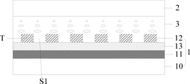
図1は従来の液晶表示パネルの構造を示す概略図である。図2は、図1における液晶表示パネルのA-A’線に沿う断面図である。図1及び図2に示すように、従来の液晶表示パネルは、アレイ基板1と、アレイ基板1に対向する対向基板2と、アレイ基板1と対向基板2との間に位置する液晶層3とを備える。液晶表示パネルは、第1電極層11、第2電極層12、及び第1電極層11と第2電極層12との間に位置する絶縁層13を含む。第2電極層は、例えば、画素電極層とすることができる。図1に示すように、画素電極層は、複数のスリットSによって離間された複数のブランチ12Bを含む。複数のブランチ12Bは、第2電極層12の底部に位置する第1バー12-1と第2電極層12の頂部に位置する第2バー12-2とによって互いに接続される。複数のスリットSの各々は、第1端部と第2端部とを有しており、この両端部は、いずれも閉合端である。例えば、第1バー12-1及び第2バー12-2は、当該スリットの第1端部及び第2端部において前記複数のスリットSの各々を閉合させる。第1電極層11は、サブ画素領域のエッジまで延在する。図1に示すように、第1電極層11のベース基板10における投影は、サブ画素領域のエッジに沿って第1電極層11の幅にわたって第2電極層12の第1バー12-1のベース基板10における投影と重なる。第1電極層11と第2電極層12との間(例えば、第1バー12-1と第2バー12-2に対応する領域内)の重なり領域が大きいので、第1電極層11と第2電極層12との間には一つの大きな蓄積容量が形成される。その蓄積容量は、以下の式によって決定され得る。
![]()
![]()
ここで、εは誘電率、Sは第1電極層11と第2電極層12との重なり面積、dは第1電極層11と第2電極層12との間の距離である。
Here, ε is the dielectric constant, S is the overlapping area between the
通常、第1電極層11及び第2電極層12は、インジウム錫酸化物、又は他の類似の金属酸化物又は透明導電材料から作製される。光は、サブ画素領域のエッジに沿って、2つの電極層を通過するようになる、例えば、まず第1電極層11を通過し、そして第1バー12-1又は第2バー12-2を通過する。従って、第1バー12-1及び第2バー12-2に対応する領域の光透過率は、例えば20%減少され、サブ画素領域のエッジに沿って暗領域が形成される。
Usually, the
よって、本開示は特に、関連技術の制限及び欠点による不具合の一つ又は複数を実質的に回避できるアレイ基板、液晶表示パネル及び液晶表示装置を提供する。一つの態様では、本開示は液晶表示パネルを提供する。幾つかの実施例において、液晶表示パネルは、アレイ基板と、アレイ基板に対向する対向基板と、複数のサブ画素とを有する液晶表示パネルである。液晶表示パネルは、各サブ画素において、アレイ基板と対向基板との間に位置する液晶層と、液晶層内に液晶分子を駆動するためのフリンジフィールドを形成するように配置される第1電極層、第2電極層と、前記第1電極層と前記第2電極層との間に位置する絶縁層とを備え;前記第2電極層は、複数のブランチを含み;前記複数のブランチは、複数の歯部にグループ化されることができ;前記複数の歯部のうち隣接する歯部は、一つの第1スリットによって離間されており、第1スリットは、第1端部E1で開放されると共に、第2端部E2で閉合され、且つ実質的に第2電極層の一つの次元にわたって延在しており、第1端部E1は第2端部E2に互いに対向し、隣接する歯部は、第1端部E1で互いに分離されると共に、第2端部E2で互いに接続される。選択的には、第1電極層は共通電極層であり、第2電極層は画素電極層である。選択的には、第2電極層は共通電極層であり、且つ第1電極層は画素電極層である。本開示の記述においては、前記複数の歯部の各々は、一つ又は複数の隣接するブランチを備えることができる。選択的には、前記複数の歯部の各々は、一つのブランチのみを備える。選択的には、前記複数の歯部の各々は、2つの隣接するブランチを備える。選択的には、前記複数の歯部の各々は、2つ以上の隣接するブランチを備える。 Accordingly, the present disclosure specifically provides an array substrate, a liquid crystal display panel and a liquid crystal display device that can substantially avoid one or more of the defects due to the limitations and drawbacks of the related art. In one aspect, the present disclosure provides a liquid crystal display panel. In some embodiments, the liquid crystal display panel is a liquid crystal display panel having an array substrate, a facing substrate facing the array substrate, and a plurality of sub-pixels. The liquid crystal display panel is a first electrode layer arranged so as to form a liquid crystal layer located between the array substrate and the facing substrate in each subpixel and a fringe field for driving the liquid crystal molecules in the liquid crystal layer. , A second electrode layer and an insulating layer located between the first electrode layer and the second electrode layer; the second electrode layer includes a plurality of branches; the plurality of branches are a plurality of branches. Can be grouped into teeth; adjacent teeth of the plurality of teeth are separated by one first slit, the first slit being opened at the first end E1. At the same time, it is closed at the second end E2 and substantially extends over one dimension of the second electrode layer, and the first end E1 faces the second end E2 and is adjacent to each other. Are separated from each other at the first end E1 and connected to each other at the second end E2. Optionally, the first electrode layer is a common electrode layer and the second electrode layer is a pixel electrode layer. Optionally, the second electrode layer is a common electrode layer, and the first electrode layer is a pixel electrode layer. In the description of the present disclosure, each of the plurality of teeth may include one or more adjacent branches. Optionally, each of the plurality of teeth comprises only one branch. Optionally, each of the plurality of teeth comprises two adjacent branches. Optionally, each of the plurality of teeth comprises two or more adjacent branches.
図3は、本開示の幾つかの実施形態に係る液晶表示パネルの構造を示す概略図である。図4は、図3における液晶表示パネルの線B-B’線に沿う断面図である。図3及び図4に示すように、幾つかの実施例に係る液晶表示パネルは、アレイ基板1と、アレイ基板1に対向する対向基板2と、アレイ基板1と対向基板2との間に位置する液晶層3とを備える。液晶表示パネルは、複数のサブ画素を有する。サブ画素の各々において、液晶表示パネルは、第1電極層11、第2電極層12、及び第1電極層11と第2電極層12との間に位置する絶縁層13を含む。第1電極層11及び第2電極層12は、液晶層3内の液晶分子を駆動するためのフリンジフィールドを形成するように配置される。液晶表示パネルは、さらに互いに交差する複数のゲート線GLと複数のデータ線DLとを備え、これによって、複数のサブ画素を限定する。サブ画素の各々は、さらにサブ画素内の画像表示を駆動するためのゲートGを有するスイッチング薄膜トランジスタを含む。第2電極層12は画素電極層である場合(図3に示すように)、第2電極層12がこのスイッチング薄膜トランジスタのドレインに接続され、且つ複数のデータ線DLのうちの一つは、このスイッチング薄膜トランジスタのソースに接続される。選択的には、第2電極層12は共通電極層であり、第1電極層11は画素電極層であり、且つ第1電極層11は、このスイッチング薄膜トランジスタのドレインに接続される。
FIG. 3 is a schematic diagram showing the structure of a liquid crystal display panel according to some embodiments of the present disclosure. FIG. 4 is a cross-sectional view taken along the line BB'of the liquid crystal display panel in FIG. As shown in FIGS. 3 and 4, the liquid crystal display panel according to some embodiments is located between the
図3に示すように、第1電極層11(例えば共通電極層)は、実質的にサブ画素にわたって延在し、例えばサブ画素の第1エッジまで延在する(例えば、図3の線B-B’に接近する)プレート電極層である。第2電極層12は複数のブランチ12Bを含み、前記複数のブランチ12Bの各々は、実質的にサブ画素の長手方向に沿って延在する。選択的には、複数のブランチ12Bは、複数のデータ線DLと実質的に平行な方向に沿って延在する。選択的には、複数のブランチ12Bは、複数のゲート線GLと実質的に平行な方向に沿って延在する。複数のブランチ12Bは、複数のスリット(例えば、図3の第1スリットS1)によって離間される。
As shown in FIG. 3, the first electrode layer 11 (eg, the common electrode layer) substantially extends over the sub-pixels, eg, extends to the first edge of the sub-pixels (eg, line B— in FIG. 3). It is a plate electrode layer (close to B'). The
幾つかの実施例において、複数のブランチ12Bは、複数の歯部Tにグループ化されることができる。図3に示す実施例において、複数のブランチ12Bの各々は、複数の歯部Tのうちの一つに対応し、例えば複数の歯部Tの各々は、複数のブランチ12Bのうちの一つのみを含む。複数の歯部Tのうち隣接する歯部は、第1スリットS1によって離間される。従って、図3に示す実施例において、複数のブランチ12Bのうち隣接するブランチは、第1スリットS1によって離間される。
In some embodiments, the plurality of
第1スリットS1は、第1端部E1(例えば、サブ画素の第1エッジに沿う第1信号線に接近する一端)で開放されると共に、第2端部E2(例えば、サブ画素の第1エッジに対向する第2エッジに沿う第2信号線に接近する一端)で閉合される。第1端部E1は第2端部E2に対向する。第1スリットS1は、隣接する歯部(又は図3に示す実施例の隣接するブランチ12B)と実質的に平行な方向に沿って延在し、第1スリットS1の第1端部E1は、複数のブランチ12Bのうちの一つのブランチの第1端部に接近すると共に、複数のブランチ12Bのうちの該一つのブランチの第2端部(複数のブランチ12Bのうちの該一つのブランチの第1端部に対向する)から離れており、さらに、第1スリットS1の第2端部E2は、複数のブランチ12Bのうちの一つのブランチの第2端部に接近すると共に、複数のブランチ12Bのうちの該一つのブランチの第1端部から離れる。第1スリットS1は、実質的に第2電極層12の一つの次元にわたって延在し、例えば、第2電極層12の長手方向の次元にわたって延在する。隣接する歯部は、第1端部E1で互いに分離されると共に、第2端部E2で互いに接続される。図3に示す実施例において、複数のブランチ12Bのうち隣接するブランチは、第1端部E1で互いに分離されると共に、第2端部E2で互いに接続される。
The first slit S1 is opened at the first end E1 (for example, one end approaching the first signal line along the first edge of the sub pixel) and the second end E2 (for example, the first of the sub pixels). It is closed at one end) approaching the second signal line along the second edge facing the edge. The first end E1 faces the second end E2. The first slit S1 extends along a direction substantially parallel to the adjacent tooth portion (or the
図3に示す実施例において、第2電極層12は、複数の歯部Tと、第2端部E2において複数の歯部Tのうち隣接する歯部を接続するバー(例えば、図3に示す第1バー12-1)とを有する櫛歯状電極層である。従来の液晶表示パネルと比べて、図3に示す液晶表示パネルは、サブ画素の一つのエッジのみに沿った一つのバーを有する、例えば、サブ画素の対向するエッジに沿った第2バーを備えない。図2と図4に示す断面図から明らかなように、本設計は、第1電極層11と第2電極層12との間の重なり面積を大幅に減少した。その結果、第1電極層11と第2電極層12との間の蓄積容量が大幅に減少された。図4に示すように、本液晶表示パネルはサブ画素のエッジに沿った複数のスリットを有し、これらの領域において、光は2つの電極層を通過する必要がない。従って、サブ画素のエッジに沿った光透過率は著しく改善され、サブ画素のエッジ沿いの暗領域発生は回避される。
In the embodiment shown in FIG. 3, the
図3に示すように、複数のブランチ12Bの各々は、実質的に第2電極層12の一つの次元(例えば、長手方向の次元)にわたって延在する。隣接する歯部又は隣接するブランチを接続するための任意の構造は、第2電極層12の周辺領域に配置される。第1スリットS1の第1端部E1及び第2端部E2は、第2電極層12の周辺領域に位置される。複数の歯部のうち隣接する歯部を接続するバーも、第2電極層12の周辺領域に位置する。
As shown in FIG. 3, each of the plurality of
図5は、本開示の幾つかの実施例に係る液晶表示パネルの構造を示す概略図である。図3に示す実施例において、隣接する歯部又は隣接するブランチを接続するバーは、サブ画素の発光を制御するためのゲート走査信号をサブ画素に提供するように配置されたゲート線に接近する第1バー12-1である。図5に示す実施例において、隣接する歯部又は隣接するブランチを接続するバーは、サブ画素の第1エッジに沿った第2バー12-2であり、前記第1エッジはサブ画素の第2エッジに対向しており、サブ画素の発光を制御するゲート線は、第2エッジに位置する。図3に示す実施例と同様に、従来の液晶表示パネルに比べて、第1電極層11と第2電極層12との間の重なり面積及び蓄積容量は、著しく減少する。サブ画素のエッジに沿った光透過率が向上され、画像表示における暗いエッジが除去されるようになる。
FIG. 5 is a schematic diagram showing the structure of a liquid crystal display panel according to some embodiments of the present disclosure. In the embodiment shown in FIG. 3, a bar connecting adjacent teeth or adjacent branches approaches a gate line arranged to provide a gate scan signal to the subpixels to control the emission of the subpixels. The first bar 12-1. In the embodiment shown in FIG. 5, the bar connecting the adjacent tooth portions or the adjacent branches is the second bar 12-2 along the first edge of the sub-pixel, and the first edge is the second of the sub-pixel. The gate line facing the edge and controlling the light emission of the sub-pixel is located at the second edge. Similar to the embodiment shown in FIG. 3, the overlapping area and the accumulated capacity between the
幾つかの実施例において、液晶表示パネルは、さらに複数の共通電極信号線を備える。図3及び図5に示すように、各サブ画素は共通電極信号線CLと関連付けられる。選択的には、共通電極信号線CLは、サブ画素の発光を制御するゲート線が位置するサブ画素の第2エッジに対向するサブ画素の第1エッジに接近する位置にある。図3に示すように、幾つかの実施例において、共通電極信号線CLのアレイ基板のベース基板における投影は、第1端部E1において複数の歯部Tのアレイ基板のベース基板における投影と少なくとも部分的に重なる。 In some embodiments, the liquid crystal display panel further comprises a plurality of common electrode signal lines. As shown in FIGS. 3 and 5, each subpixel is associated with a common electrode signal line CL. Optionally, the common electrode signal line CL is located close to the first edge of the subpixel facing the second edge of the subpixel where the gate line controlling the emission of the subpixel is located. As shown in FIG. 3, in some embodiments, the projection of the common electrode signal line CL on the base substrate of the array substrate is at least the projection on the base substrate of the array substrate of the plurality of tooth portions T at the first end E1. Partially overlap.
図5に示すように、幾つかの実施例において、共通電極信号線CLのアレイ基板のベース基板における投影は、第2バー12-2のアレイ基板のベース基板における投影と少なくとも部分的に重なる。選択的には、共通電極信号線CLのアレイ基板のベース基板における投影は、第2バー12-2のアレイ基板のベース基板における投影と実質的に重なる。選択的には、共通電極信号線CLのアレイ基板のベース基板における投影は、第2バー12-2のアレイ基板のベース基板における投影を完全に覆う。サブ画素領域内の共通電極信号線CLに対応する領域は、暗領域である。バーを少なくとも部分的に共通電極信号線CLに対応する領域に位置させるように配置することによって、表示パネルの開口率及び光透過率は、バーから最小限の影響を受けるか、又はバーからの影響を受けさせない。 As shown in FIG. 5, in some embodiments, the projection of the common electrode signal line CL on the base substrate of the array substrate overlaps at least partially with the projection of the second bar 12-2 on the base substrate of the array substrate. Optionally, the projection of the common electrode signal line CL on the base substrate of the array substrate substantially overlaps with the projection on the base substrate of the array substrate of the second bar 12-2. Optionally, the projection of the common electrode signal line CL on the base substrate of the array substrate completely covers the projection on the base substrate of the array substrate of the second bar 12-2. The region corresponding to the common electrode signal line CL in the sub-pixel region is a dark region. By arranging the bar at least partially so as to be located in the region corresponding to the common electrode signal line CL, the aperture ratio and light transmittance of the display panel are minimally affected by the bar or from the bar. Not affected.
幾つかの実施例において、図3及び図5に示すように、共通電極信号線CLは、複数のゲート線GLと同じ層に位置する。選択的には、共通電極信号線CLと複数のゲート線GLとは、同じ材料からなり、且つ同じマスクプレートによってパターニングされる。幾つかの実施例において、共通電極信号線CLは、複数のゲート線GLと異なる層に位置する。 In some embodiments, as shown in FIGS. 3 and 5, the common electrode signal line CL is located on the same layer as the plurality of gate lines GL. Optionally, the common electrode signal line CL and the plurality of gate lines GL are made of the same material and are patterned by the same mask plate. In some embodiments, the common electrode signal line CL is located on a different layer than the plurality of gate lines GL.
図6は、本開示の幾つかの実施形態に係る液晶表示パネルの構造を示す概略図である。図7は、図6における液晶表示パネルの線C-C’線に沿う断面図である。図8は、図6における液晶表示パネルの線D-D’線に沿う断面図である。図6~図8に示すように、サブ画素の各々において、幾つかの実施例に係る液晶表示パネルは、第1電極層11、第2電極層12、及び第1電極層11と第2電極層12との間に位置する絶縁層13を含む。第1電極層11及び第2電極層12は、液晶層3内の液晶分子を駆動するためのフリンジフィールドを形成するように配置される。選択的には、第2電極層12は共通電極層であり、第1電極層11は画素電極層であり、且つ第1電極層11はスイッチング薄膜トランジスタのドレインに接続される。
FIG. 6 is a schematic diagram showing the structure of a liquid crystal display panel according to some embodiments of the present disclosure. FIG. 7 is a cross-sectional view taken along the line CC'of the liquid crystal display panel in FIG. FIG. 8 is a cross-sectional view taken along the line DD'of the liquid crystal display panel in FIG. As shown in FIGS. 6 to 8, in each of the sub-pixels, the liquid crystal display panel according to some embodiments is the
図6に示すように、第1電極層11(例えば、共通電極層)は、実質的にサブ画素領域にわたって延在し、例えばサブ画素の第1エッジまで延在する(例えば、図6の線C-C’線に接近する)プレート電極層である。第2電極層12は複数のブランチ12B(例えば、図6の第1ブランチ12B1と第2ブランチ12B2)を含み、前記複数のブランチ12Bの各々は、実質的にサブ画素の長手方向に沿って延在する。複数のブランチ12Bは、複数のスリット(例えば、図6の第1スリットS1と第2スリットS2)によって離間される。
As shown in FIG. 6, the first electrode layer 11 (eg, the common electrode layer) substantially extends over the subpixel region, eg, extends to the first edge of the subpixel (eg, line of FIG. 6). It is a plate electrode layer (close to the CC'line). The
幾つかの実施例において、複数のブランチ12Bは、複数の歯部Tにグループ化されることができる。図6に示す実施例において、複数の歯部Tの各々は、複数のブランチ12Bのうちの第1ブランチ12B1と第2ブランチ12B2とを含む。第1ブランチ12B1と第2ブランチ12B2は、図6の線C-C’に接近するサブ画素の第1エッジに沿って互いに接続される。複数の歯部Tのうち隣接する歯部は、第1スリットS1によって離間される。複数の歯部Tの各々における第1ブランチ12B1と第2ブランチ12B2は、第2スリットS2によって離間される。
In some embodiments, the plurality of
第1スリットS1は、第1端部E1(例えば、サブ画素の第1エッジに沿った第1信号線に接近する一端)で開放されると共に、第2端部E2(例えば、サブ画素の第1エッジに対向する第2エッジに沿った第2信号線に接近する一端)で閉合される。第1端部E1は第2端部E2に対向する。第1スリットS1は、隣接する歯部(又は図6に示す実施例の隣接するブランチ12B)と実質的に平行な方向に沿って延在し、第1スリットS1の第1端部E1は、複数の歯部Tのうちの一つの歯部の第1端部に接近すると共に、複数の歯部Tのうちの該一つの歯部の第2端部(複数の歯部Tのうちの該一つの歯部の第1端部に対向する)から離れており、且つ、第1スリットS1の第2端部E2は、複数の歯部Tのうちの一つの歯部の第2端部に接近すると共に、複数の歯部Tのうちの該一つの歯部の第1端部から離れる。第1スリットS1は、実質的に第2電極層12の一つの次元にわたって延在する、例えば、第2電極層12の長手方向の次元にわたって延在する。隣接する歯部は、第1端部E1で互いに分離されると共に、第2端部E2で互いに接続される。ここで、第1スリットS1が実質的に第2電極層12の一つの次元にわたって延在するとは、第1スリットS1のその延在方向に沿った長さが第2の電極層12の対応する一つの次元よりも小さいが、それに近いことを指す。
The first slit S1 is opened at the first end E1 (for example, one end approaching the first signal line along the first edge of the sub pixel) and the second end E2 (for example, the first of the sub pixels). It is closed at one end) approaching the second signal line along the second edge facing the first edge. The first end E1 faces the second end E2. The first slit S1 extends along a direction substantially parallel to the adjacent tooth portion (or the
第2スリットS2は、第3端部E3(例えば、サブ画素の第1エッジに沿った第1信号線に接近する一端)で閉合され、且つ第4端部E4(例えば、サブ画素の第1エッジに対向する第2エッジに沿った第2信号線に接近する)で開放される。第3端部E3は第4端部E4に対向する。第2スリットS2は、複数の歯部Tのうちの各々における第1ブランチ12B1及び第2ブランチ12B2と実質的に平行な方向に沿って延在し、第2スリットS2の第3端部E3は、複数の歯部Tのうちの一つの歯部の第1端部に接近すると共に、複数の歯部Tのうちの該一つの歯部の第2端部(複数の歯部Tのうちの該一つの歯部の第1端部に対向する)から離れ、且つ、第2スリットS2の第4端部E4は、複数の歯部Tのうちの一つの歯部の第2端部に接近すると共に、複数の歯部Tのうちの該一つの歯部の第1端部から離れる。第2スリットS2は、実質的に第2電極層12の一つの次元にわたって延在し、例えば、第2電極層12の長手方向の次元にわたって延在する。ここで、第2スリットS2が実質的に第2電極層12の一つの次元にわたって延在するとは、第2スリットS2のその延在方向に沿った長さが第2の電極層12の一つの次元よりも小さいが、それに近いことを指す。
The second slit S2 is closed at the third end E3 (eg, one end approaching the first signal line along the first edge of the subpixel) and the fourth end E4 (eg, the first of the subpixels). It approaches the second signal line along the second edge facing the edge). The third end E3 faces the fourth end E4. The second slit S2 extends along a direction substantially parallel to the first branch 12B1 and the second branch 12B2 in each of the plurality of tooth portions T, and the third end E3 of the second slit S2 , Approaching the first end of one tooth of the plurality of teeth T, and the second end of the one tooth of the plurality of teeth T (of the plurality of teeth T). Away from the first end of the one tooth), and the fourth end E4 of the second slit S2 approaches the second end of one of the plurality of teeth T. At the same time, the tooth portion T is separated from the first end portion of the one tooth portion. The second slit S2 extends substantially over one dimension of the
幾つかの実施例において、第2スリットS2は第1スリットS1と実質的に平行である。選択的には、第3端部E3は、第1端部E1に接近すると共に、第2端部E2から離れており、第4端部E4は、第2端部E2に接近すると共に、第1端部E1から離れる。選択的には、第1ブランチ12B1と第2ブランチ12B2とは、第4端部E4で互いに分離されると共に、第3端部E3で互いに接続される。 In some embodiments, the second slit S2 is substantially parallel to the first slit S1. Optionally, the third end E3 is approaching the first end E1 and away from the second end E2, and the fourth end E4 is approaching and away from the second end E2. Move away from one end E1. Optionally, the first branch 12B1 and the second branch 12B2 are separated from each other at the fourth end E4 and connected to each other at the third end E3.
幾つかの実施例において、第2電極層12は、ジグザグ形状の電極層である。図6に示すように、液晶表示パネルは、サブ画素の第1エッジと第2エッジの両方に沿って複数の歯部Tを含む。図7及び図8に示すように、本液晶表示パネルはサブ画素の2つのエッジに沿った複数のスリットを有する。従来の液晶表示パネルに比べて、図6~図8の実施例に示す液晶表示パネルは、第1電極層11と第2電極層12との間の重なり面積が大幅に減少される。第1電極層11と第2電極層12との間の蓄積容量が大幅に減少される。サブ画素の二つのエッジに沿った複数のスリット領域において、光は2つの電極層を通過する必要がない。従って、サブ画素のエッジに沿って光透過率は著しく改善され、サブ画素のエッジ沿いの暗領域発生は回避される。
In some embodiments, the
図3~図7に示す実施例において、複数のブランチは、実質的にサブ画素の長手方向に沿って延在する。選択的には、複数のブランチは、実質的にサブ画素の横方向に沿って延在する。 In the embodiments shown in FIGS. 3-7, the plurality of branches substantially extend along the longitudinal direction of the subpixels. Optionally, the plurality of branches substantially extend along the lateral direction of the subpixels.
選択的には、第1電極層11及び第2電極層12は、両方ともにアレイ基板1内に位置する。
Optionally, both the
図6に示すように、複数のブランチ12Bの各々は、実質的に第2電極層12の一つの次元(例えば、長手方向の次元)にわたって延在する。隣接する歯部又は隣接するブランチを接続する如何なる構造も、第2電極層12の周辺領域に配置される。第1スリットS1の第1端部E1、第2端部E2及び第2スリットS2の第3端部E3、第4端部E4は、第2電極層12の周辺領域に位置する。
As shown in FIG. 6, each of the plurality of
幾つかの実施例において、第2電極層12は、モノドメイン電極層である。幾つかの実施例において、第2電極層12は、マルチドメイン電極層である。選択的には、第2電極層12は、第1ドメインと第2ドメインとを有し、第1ドメインにおけるブランチ及びスリットは、実質的に第1方向に沿って延在し、第2ドメインにおけるブランチ及びスリットは、実質的に第2方向に沿って延在する。
In some embodiments, the
図9は、従来の液晶表示パネルの構造を示す概略図である。図9に示すように、従来の液晶表示パネルは、サブ画素の各々において、第1電極層11と第2電極層12とを有する。幾つかの実施例における第2電極層12は、第1ドメイン(トップドメイン)と第2ドメイン(ボトムドメイン)とを有する。第2電極層12は、複数のスリットSによって離間された複数のブランチ12Bを含む。第1ドメインにおける複数のブランチ12Bは、実質的に第1方向に沿って延在する。第2ドメインにおける複数のブランチ12Bは、実質的に第2方向に沿って延在する。複数のブランチ12Bは、第2電極層12の左側に位置する第1バー12-1と第2電極層12の右側に位置する第2バー12-2とによって互いに接続される。複数のスリットSの各々は、第1端部と第2端部とを有しており、その両方は、いずれも閉合端である。例えば、第1バー12-1及び第2バー12-2は、前記複数のスリットSの各々を該スリットの第1端部及び第2端部で閉合させる。第1電極層11は、サブ画素のエッジまで延在する。第1電極層11のベース基板10における投影は、サブ画素のエッジに沿って第1電極層11の長さにわたって第2電極層12の第1バー12-1のベース基板10における投影と重なる。第1電極層11と第2電極層12との間の重なり面積が大きいため、第1電極層11と第2電極層12との間に大きな蓄積容量が形成され、且つ第1バー12-1及び第2バー12-2に対応する領域の光透過率は減少される。
FIG. 9 is a schematic view showing the structure of a conventional liquid crystal display panel. As shown in FIG. 9, the conventional liquid crystal display panel has a
図10は、本開示の幾つかの実施例に係る液晶表示パネルの構造を示す概略図である。図10に示すように、第1電極層11(例えば、共通電極層)は、実質的にサブ画素領域にわたって延在し、例えばサブ画素の第1エッジまで延在する(例えば、サブ画素の右縦エッジ)プレート電極層である。第2電極層12は複数のブランチ12Bを含み、前記複数のブランチ12Bの各々は、実質的にサブ画素の横方向に沿って延在する。複数のブランチ12Bは、複数のスリット(例えば、図10の第1スリットS1)によって離間される。複数のブランチ12Bは、複数の歯部Tにグループ化されることができる。図10に示す実施例において、複数のブランチ12Bの各々は、複数の歯部Tのうちの一つに対応し、例えば複数の歯部Tの各々は、複数のブランチ12Bのうちの一つのみを含む。複数の歯部Tのうち隣接する歯部は、第1スリットS1によって離間される。従って、図10に示す実施例において、複数のブランチ12Bのうち隣接するブランチは、第1スリットS1によって離間される。
FIG. 10 is a schematic diagram showing the structure of a liquid crystal display panel according to some embodiments of the present disclosure. As shown in FIG. 10, the first electrode layer 11 (eg, the common electrode layer) substantially extends over the subpixel region, eg, extends to the first edge of the subpixel (eg, to the right of the subpixel). Vertical edge) Plate electrode layer. The
第1スリットS1は、第1端部E1(例えば、サブ画素の第1エッジに沿った第1信号線に接近する一端)で開放されると共に、第2端部E2(例えば、サブ画素の第1エッジに対向する第2エッジに沿った第2信号線に接近する一端)で閉合される。第1端部E1は第2端部E2に対向する。第1スリットS1は、隣接する歯部(又は図10に示す実施例の隣接するブランチ)と実質的に平行な方向に沿って延在し、第1スリットS1の第1端部E1は、複数のブランチ12Bのうちの一つのブランチの第1端部に接近すると共に、複数のブランチ12Bのうちの該一つのブランチの第2端部(複数のブランチ12Bのうちの該一つのブランチの第1端部に対向する)から離れており、且つ、第1スリットS1の第2端部E2は、複数のブランチ12Bのうちの一つのブランチの第2端部に接近すると共に、複数のブランチ12Bのうちの該一つのブランチの第1端部から離れる。第1スリットS1は、実質的に第2電極層12の一つの次元にわたって延在する、例えば、第2電極層12の横方向の次元にわたって延在する。隣接する歯部は、第1端部E1で互いに分離されると共に、第2端部E2で互いに接続される。図10に示す実施例において、複数のブランチ12Bのうち隣接するブランチは、第1端部E1では互いに分離されると共に、第2端部E2で互いに接続される。
The first slit S1 is opened at the first end E1 (for example, one end approaching the first signal line along the first edge of the sub pixel) and the second end E2 (for example, the first of the sub pixels). It is closed at one end) approaching the second signal line along the second edge facing the first edge. The first end E1 faces the second end E2. The first slit S1 extends along a direction substantially parallel to the adjacent tooth portion (or the adjacent branch of the embodiment shown in FIG. 10), and the first end portion E1 of the first slit S1 has a plurality of portions. Close to the first end of one of the
図10に示す第2電極層12は、複数の歯部Tと、第2端部E2において複数の歯部Tのうち隣接する歯部を接続するバー(例えば、図10に示す第1バー12-1)とを有する櫛歯状電極層である。複数のブランチ12Bの各々は、実質的に第2電極層12の一つの次元(例えば、横方向の次元)にわたって延在する。隣接する歯部又は隣接するブランチを接続する如何なる構造も、第2電極層12の周辺領域に配置される。第1スリットS1の第1端部E1及び第2端部E2は、第2電極層12の周辺領域に位置される。複数の歯部のうち隣接する歯部を接続するバーも、第2電極層12の周辺領域に位置する。
The
図11は、本開示の幾つかの実施形態に係る液晶表示パネルの構造を示す概略図である。図11において、隣接する歯部又は隣接するブランチを接続するバーは、サブ画素の右側エッジに沿った第2バー12-2である。図10に示す実施例と同様に、従来の液晶表示パネルに比べて、第1電極層11と第2電極層12との間の重なり面積及び蓄積容量は、著しく減少される。サブ画素のエッジ沿いの光透過率が向上され、画像表示における暗いエッジが除去される。
FIG. 11 is a schematic diagram showing the structure of a liquid crystal display panel according to some embodiments of the present disclosure. In FIG. 11, the bar connecting the adjacent teeth or adjacent branches is the second bar 12-2 along the right edge of the subpixel. Similar to the embodiment shown in FIG. 10, the overlapping area and the accumulated capacity between the
図12は、本開示の幾つかの実施形態に係る液晶表示パネルの構造を示す概略図である。図12に示すように、第2電極層12は複数のブランチ12B(例えば、図12の第1ブランチ12B1と第2ブランチ12B2)を有し、前記複数のブランチ12Bの各々は、実質的にサブ画素の横方向に沿って延在する。複数のブランチ12Bは、複数のスリット(例えば、図12の第1スリットS1と第2スリットS2)によって離間される。複数のブランチ12Bは、複数の歯部Tにグループ化される、例えば、図12において、複数の歯部Tの各々は、複数のブランチ12Bのうちの第1ブランチ12B1と第2ブランチ12B2とを有する。第1ブランチ12B1と第2ブランチ12B2は、サブ画素の右側エッジに沿って互いに接続される。複数の歯部Tのうち隣接する歯部は、第1スリットS1によって離間される。複数の歯部Tのうちの各々における第1ブランチ12B1と第2ブランチ12B2は、第2スリットS2によって離間される。
FIG. 12 is a schematic diagram showing the structure of a liquid crystal display panel according to some embodiments of the present disclosure. As shown in FIG. 12, the
第1スリットS1は、第1端部E1で開放されると共に、第2端部E2で閉合されており、第1端部E1は第2端部E2に対向する。第1スリットS1は、隣接する歯部又は隣接するブランチと実質的に平行な方向に沿って延在する。第1スリットS1は、実質的に第2電極層12の一つの次元にわたって延在する、例えば、第2電極層12の横方向の次元にわたって延在する。隣接する歯部は、第1端部E1で互いに分離されると共に、第2端部E2で互いに接続される。第2スリットS2は、第3端部E3で閉合されると共に、第4端部E4で開放されており、第3端部E3は第4端部E4に対向する。第2スリットS2は、複数の歯部Tのうちの各々における第1ブランチ12B1及び第2ブランチ12B2と実質的に平行な方向に沿って延在する。第2スリットS2は、実質的に第2電極層12の一つの次元にわたって延在する、例えば、第2電極層12の横方向の次元にわたって延在する。幾つかの実施例において、第2スリットS2は第1スリットS1と実質的に平行である。選択的には、第3端部E3は、第1端部E1に接近すると共に、第2端部E2から離れており、第4端部E4は、第2端部E2に接近すると共に、第1端部E1から離れる。選択的には、第1ブランチ12B1と第2ブランチ12B2とは、第4端部E4で互いに分離されると共に、第3端部E3で互いに接続される。図12における第2電極層12は、ジグザグ形状の電極層である。液晶表示パネルは、サブ画素の左エッジと右エッジの両者に沿って複数の歯部Tを含む。
The first slit S1 is opened at the first end E1 and closed at the second end E2, and the first end E1 faces the second end E2. The first slit S1 extends along a direction substantially parallel to the adjacent tooth portion or adjacent branch. The first slit S1 extends substantially over one dimension of the
図9~図12に示すように、複数のブランチ12Bの各々は、実質的に第2電極層12の一つの次元(例えば、横方向の次元)にわたって延在する。隣接する歯部又は隣接するブランチを接続する如何なる構造も、第2電極層12の周辺領域に配置される。第1スリットS1の第1端部E1、第2端部E2及び第2スリットS2の第3端部E3、第4端部E4は、第2電極層12の周辺領域に位置される。
As shown in FIGS. 9-12, each of the plurality of
幾つかの実施例において、液晶表示パネは、フリンジフィールド駆動液晶表示パネルであり、その中の液晶層はフリンジ電界により駆動される。フリンジフィールド駆動液晶表示パネルの例示としては、高級超次元スイッチング(Advanced super Dimension Switching:ADS)型液晶表示パネル、インプレーンスイッチング(IPS)型液晶表示パネル及びフリンジフィールドスイッチング(FFS)型液晶パネルが挙げられるが、これらに限定されない。 In some embodiments, the liquid crystal display panel is a fringe field driven liquid crystal display panel in which the liquid crystal layer is driven by a fringe electric field. Examples of the fringe field drive liquid crystal display panel include an advanced super dimensional switching (ADS) type liquid crystal display panel, an inplane switching (IPS) type liquid crystal display panel, and a fringe field switching (FFS) type liquid crystal display panel. However, it is not limited to these.
もう一つの態様では、本発明は、本明細書に記載の液晶表示パネルを備える液晶表示装置を提供する。表示装置の好適な例示としては、電子ペーパー、携帯電話、タブレットコンピュータ、テレビ、モニタ、ノートブックコンピュータ、デジタルフォトアルバム、ゲームシステム等が挙げられるが、これらに限定されない。 In another aspect, the invention provides a liquid crystal display device comprising the liquid crystal display panel described herein. Preferable examples of the display device include, but are not limited to, electronic paper, mobile phones, tablet computers, televisions, monitors, notebook computers, digital photo albums, game systems and the like.
本発明の実施例の上述した説明は、例示及び説明を目的とする。それらは網羅的であること、又は本発明を開示された精確な形態又は例示的な実施例に限定することを意図していない。従って、上記の説明は、限定的ではなく、例示的と理解されるべきである。種々の変形や変更を行うことができるということは当業者には明らかであろう。これらの実施例を選択して説明するのは、本発明の原理及び最良の実施形態の実際の適用を解釈することにより、当業者に種々の実施例、及び特定用途や構想された実施形態に適した様々な変形例を通じて本発明を理解させるためである。本発明の範囲は、添付の特許請求の範囲及びそれらの均等の形態によって限定されることを意図しており、特に言及しない限り、全ての用語は、それらの最も広く、合理的な意味で理解されるべきである。従って、「前記発明」、「本発明」などの用語は、必ずしも特許請求の範囲を特定の実施例に限定することを意図するものではなく、本発明の例示的な実施例への言及は、本発明を限定することを意図するものではないし、そのような制限も推断されるべきではない。本発明は、添付の特許請求の範囲の精神及び範囲のみによって限定される。さらに、これらの請求項では、名詞又はエレメントの前に「第1」、「第2」等を付しても良い。これらの用語は命名法として理解されるべきであり、特定の数が与えられていない限り、これらの命名法によって修飾されるエレメントの数を限定するものとして理解されるべきではない。説明された如何なる利点及び効果も、本発明の全ての実施例に適用しなくてもよい。添付の特許請求の範囲によって限定された本発明の範囲から逸脱しない範囲内において、当業者であればここに記載の実施例に対して様々な変形をなし得ると理解されるべきである。さらに、本開示における如何なるエレメント及び構成要素も、添付の特許請求の範囲に明確に記載されているか否かにかかわらず、公衆に捧げることを意図するものではない。 The above description of the embodiments of the present invention is for purposes of illustration and description. They are not intended to be exhaustive or to limit the invention to the disclosed precise embodiments or exemplary examples. Therefore, the above description should be understood as exemplary rather than limiting. It will be apparent to those skilled in the art that various modifications and changes can be made. These embodiments will be selected and described to those skilled in the art by interpreting the principles of the invention and the actual application of the best embodiments to various embodiments and specific uses and conceived embodiments. This is for the purpose of understanding the present invention through various suitable modifications. The scope of the invention is intended to be limited by the appended claims and their equivalent forms, and unless otherwise stated, all terms are understood in their broadest and most rational sense. It should be. Therefore, terms such as "the invention" and "the present invention" are not necessarily intended to limit the scope of claims to specific embodiments, and references to exemplary embodiments of the present invention are made. It is not intended to limit the invention and such restrictions should not be inferred. The present invention is limited only by the spirit and scope of the appended claims. Further, in these claims, "first", "second" and the like may be added before the noun or element. These terms should be understood as nomenclatures and should not be understood as limiting the number of elements modified by these nomenclatures unless a particular number is given. Any of the advantages and effects described may not apply to all embodiments of the invention. It should be understood that one of ordinary skill in the art may make various modifications to the embodiments described herein within the scope of the invention limited by the appended claims. Moreover, no element or component in this disclosure is intended to be dedicated to the public, whether or not expressly stated in the appended claims.
Claims (12)
前記アレイ基板は、前記複数のサブ画素領域の一つのサブ画素領域は、
液晶分子を駆動するためのフリンジフィールドを形成するように配置される第1電極層、第2電極層と、
前記第1電極層と前記第2電極層との間に位置する絶縁層とを備え、
前記第2電極層は、複数のブランチを含み、前記複数のブランチは、実質的に前記データ線に平行な方向に沿って延在し、
前記複数のブランチは、複数の歯部にグループ化され、
前記複数の歯部のうち隣接する歯部は、第1スリットによって離間されており、前記第1スリットは、実質的に前記複数のサブ画素領域のうちの一つのサブ画素領域における前記第2電極層の一つの次元にわたって延在し、
隣接する歯部は、第1端部で互いに分離されると共に、第2端部で互いに接続され、
前記複数の歯部の一つは、前記複数のブランチのうちの第1ブランチと第2ブランチとを含み、且つ、
前記第1ブランチと前記第2ブランチとは、第2スリットによって離間されており、前記第2スリットは、実質的に前記第2電極層の前記一つの次元にわたって延在し、
前記第2スリットは、前記第1スリットと実質的に平行であり、
前記第1ブランチと前記第2ブランチは、第3端部で互いに接続され、そして第4端部で互いに分離され、
前記第3端部は、前記第1端部に接近すると共に前記第2端部から離れており、
前記第4端部は、前記第2端部に接近すると共に前記第1端部から離れ、
前記第3端部に対応する位置における前記第2電極層の前記アレイ基板における正投影と、前記共通電極信号線の前記アレイ基板における正投影とは、複数の重なり部分があり、且つ、
前記データ線の延在方向と前記共通電極信号線の延在方向とは直交する、
アレイ基板。 An array substrate having a plurality of sub-pixel regions defined by using a data line and a common electrode signal line .
In the array substrate, one sub-pixel area of the plurality of sub-pixel areas is
A first electrode layer, a second electrode layer, and a second electrode layer arranged so as to form a fringe field for driving liquid crystal molecules.
An insulating layer located between the first electrode layer and the second electrode layer is provided.
The second electrode layer contains a plurality of branches, the plurality of branches extending in a direction substantially parallel to the data line .
The plurality of branches are grouped into a plurality of teeth, and the plurality of branches are grouped into a plurality of teeth.
The adjacent tooth portions of the plurality of tooth portions are separated by a first slit, and the first slit is substantially the second electrode in one sub-pixel region of the plurality of sub-pixel regions. Extending over one dimension of the layer,
Adjacent teeth are separated from each other at the first end and connected to each other at the second end.
One of the plurality of teeth includes a first branch and a second branch of the plurality of branches, and the plurality of teeth are included.
The first branch and the second branch are separated by a second slit, which substantially extends over the one dimension of the second electrode layer.
The second slit is substantially parallel to the first slit.
The first branch and the second branch are connected to each other at the third end and separated from each other at the fourth end.
The third end is close to the first end and away from the second end.
The fourth end approaches the second end and separates from the first end .
The orthogonal projection of the second electrode layer on the array substrate at the position corresponding to the third end portion and the orthogonal projection of the common electrode signal line on the array substrate have a plurality of overlapping portions, and
The extending direction of the data line and the extending direction of the common electrode signal line are orthogonal to each other.
Array board.
前記アレイ基板1に対向する対向基板と、
前記アレイ基板1と前記対向基板2との間に位置する液晶層とを備える、液晶表示パネル。 The array substrate according to any one of claims 1 to 8,
The facing board facing the array board 1 and the facing board
A liquid crystal display panel including a liquid crystal layer located between the array substrate 1 and the facing substrate 2.
Applications Claiming Priority (1)
| Application Number | Priority Date | Filing Date | Title |
|---|---|---|---|
| PCT/CN2017/079339 WO2018176483A1 (en) | 2017-04-01 | 2017-04-01 | Array substrate, liquid crystal display panel and liquid crystal display apparatus |
Publications (2)
| Publication Number | Publication Date |
|---|---|
| JP2020513111A JP2020513111A (en) | 2020-04-30 |
| JP7004734B2 true JP7004734B2 (en) | 2022-02-10 |
Family
ID=63674058
Family Applications (1)
| Application Number | Title | Priority Date | Filing Date |
|---|---|---|---|
| JP2019548984A Active JP7004734B2 (en) | 2017-04-01 | 2017-04-01 | Array board, liquid crystal display panel and liquid crystal display device |
Country Status (5)
| Country | Link |
|---|---|
| US (1) | US20200249534A1 (en) |
| EP (1) | EP3607398B1 (en) |
| JP (1) | JP7004734B2 (en) |
| CN (1) | CN109154749A (en) |
| WO (1) | WO2018176483A1 (en) |
Families Citing this family (1)
| Publication number | Priority date | Publication date | Assignee | Title |
|---|---|---|---|---|
| CN114660856B (en) * | 2022-03-16 | 2024-02-20 | Tcl华星光电技术有限公司 | Array substrate and display device |
Citations (8)
| Publication number | Priority date | Publication date | Assignee | Title |
|---|---|---|---|---|
| JP2001059976A (en) | 1999-06-30 | 2001-03-06 | Hyundai Electronics Ind Co Ltd | Liquid crystal display device and its manufacturing method |
| JP2001228493A (en) | 1999-12-29 | 2001-08-24 | Hynix Semiconductor Inc | Method of manufacturing for thin film transistor liquid crystal display device |
| US20040227875A1 (en) | 1998-06-30 | 2004-11-18 | Park In Cheol | Reflective liquid crystal display of high aperture ratio, high transmittance and wide viewing angle |
| JP2007327997A (en) | 2006-06-06 | 2007-12-20 | Epson Imaging Devices Corp | Liquid crystal device and electronic equipment |
| CN101995700A (en) | 2009-08-10 | 2011-03-30 | 北京京东方光电科技有限公司 | Liquid crystal panel and manufacturing method thereof |
| CN103185993A (en) | 2011-12-29 | 2013-07-03 | 上海天马微电子有限公司 | Array substrate of IPS (in-plane switching)/FFS (fringe field switching) liquid crystal display device |
| JP2014228565A (en) | 2013-05-17 | 2014-12-08 | パナソニック液晶ディスプレイ株式会社 | Liquid crystal display device and manufacturing method of liquid crystal display device |
| JP2015520940A (en) | 2012-04-24 | 2015-07-23 | 京東方科技集團股▲ふん▼有限公司 | Organic thin film transistor array substrate, method for manufacturing the same, and display device |
Family Cites Families (10)
| Publication number | Priority date | Publication date | Assignee | Title |
|---|---|---|---|---|
| TW387997B (en) * | 1997-12-29 | 2000-04-21 | Hyundai Electronics Ind | Liquid crystal display and fabrication method |
| KR20000039794A (en) * | 1998-12-16 | 2000-07-05 | 김영환 | Method for manufacturing liquid crystal display device with high aperture rate and high transparency |
| JP4201051B2 (en) | 2006-09-15 | 2008-12-24 | エプソンイメージングデバイス株式会社 | LCD panel |
| CN100565313C (en) * | 2006-09-15 | 2009-12-02 | 爱普生映像元器件有限公司 | LCD panel |
| JP4600463B2 (en) * | 2007-11-21 | 2010-12-15 | ソニー株式会社 | Liquid crystal display |
| KR20090116856A (en) * | 2008-05-08 | 2009-11-12 | 전북대학교산학협력단 | Fringe in-plane field switching liquid crystal display |
| US8953132B2 (en) | 2011-03-30 | 2015-02-10 | Au Optronics Corp. | Pixel array of fringe field switching liquid crystal display panel and driving method thereof |
| CN203894515U (en) * | 2014-06-13 | 2014-10-22 | 京东方科技集团股份有限公司 | Array substrate and display device |
| CN105137680B (en) * | 2015-10-20 | 2018-11-06 | 京东方科技集团股份有限公司 | A kind of liquid crystal display electrode, array substrate, display panel, display device |
| CN105676550A (en) * | 2016-04-21 | 2016-06-15 | 京东方科技集团股份有限公司 | Array substrate, manufacturing method thereof and display device |
-
2017
- 2017-04-01 EP EP17903368.3A patent/EP3607398B1/en active Active
- 2017-04-01 US US15/761,347 patent/US20200249534A1/en not_active Abandoned
- 2017-04-01 JP JP2019548984A patent/JP7004734B2/en active Active
- 2017-04-01 WO PCT/CN2017/079339 patent/WO2018176483A1/en unknown
- 2017-04-01 CN CN201780000183.9A patent/CN109154749A/en active Pending
Patent Citations (8)
| Publication number | Priority date | Publication date | Assignee | Title |
|---|---|---|---|---|
| US20040227875A1 (en) | 1998-06-30 | 2004-11-18 | Park In Cheol | Reflective liquid crystal display of high aperture ratio, high transmittance and wide viewing angle |
| JP2001059976A (en) | 1999-06-30 | 2001-03-06 | Hyundai Electronics Ind Co Ltd | Liquid crystal display device and its manufacturing method |
| JP2001228493A (en) | 1999-12-29 | 2001-08-24 | Hynix Semiconductor Inc | Method of manufacturing for thin film transistor liquid crystal display device |
| JP2007327997A (en) | 2006-06-06 | 2007-12-20 | Epson Imaging Devices Corp | Liquid crystal device and electronic equipment |
| CN101995700A (en) | 2009-08-10 | 2011-03-30 | 北京京东方光电科技有限公司 | Liquid crystal panel and manufacturing method thereof |
| CN103185993A (en) | 2011-12-29 | 2013-07-03 | 上海天马微电子有限公司 | Array substrate of IPS (in-plane switching)/FFS (fringe field switching) liquid crystal display device |
| JP2015520940A (en) | 2012-04-24 | 2015-07-23 | 京東方科技集團股▲ふん▼有限公司 | Organic thin film transistor array substrate, method for manufacturing the same, and display device |
| JP2014228565A (en) | 2013-05-17 | 2014-12-08 | パナソニック液晶ディスプレイ株式会社 | Liquid crystal display device and manufacturing method of liquid crystal display device |
Also Published As
| Publication number | Publication date |
|---|---|
| WO2018176483A9 (en) | 2018-11-15 |
| CN109154749A (en) | 2019-01-04 |
| JP2020513111A (en) | 2020-04-30 |
| EP3607398A4 (en) | 2020-09-02 |
| EP3607398A1 (en) | 2020-02-12 |
| WO2018176483A1 (en) | 2018-10-04 |
| US20200249534A1 (en) | 2020-08-06 |
| EP3607398B1 (en) | 2022-01-12 |
Similar Documents
| Publication | Publication Date | Title |
|---|---|---|
| US10459302B2 (en) | Array substrate, display panel and display device | |
| TWI509482B (en) | Liquid crystal display device with a built-in touch panel | |
| JP5875001B2 (en) | Horizontal electric field type liquid crystal display device | |
| JP7142756B2 (en) | Display device | |
| US9196634B2 (en) | TFT array substrate, display panel and display device | |
| TWI468826B (en) | Pixel array substrate | |
| US9335591B2 (en) | Array substrate, display panel and display device | |
| WO2016107098A1 (en) | Touch substrate and touch device | |
| US10317737B2 (en) | Array substrate, display panel and display device | |
| US9360727B1 (en) | Pixel structure of display panel | |
| JP5127485B2 (en) | Liquid crystal display | |
| US8947608B2 (en) | Display apparatus including electrostatic preventing pattern | |
| US9146423B2 (en) | Pixel structure | |
| JP6356469B2 (en) | Liquid crystal display | |
| US20160026043A1 (en) | Display device | |
| US9946117B2 (en) | Display device | |
| JP6336762B2 (en) | Liquid crystal display | |
| WO2019080596A1 (en) | Array substrate and display device | |
| JP7004734B2 (en) | Array board, liquid crystal display panel and liquid crystal display device | |
| KR20100122404A (en) | Fringe field switching liquid crystal display device and method of fabricating the same | |
| JP6488407B2 (en) | Array substrate and liquid crystal display device | |
| WO2019200964A1 (en) | Display substrate and display device | |
| JP6400935B2 (en) | Display device | |
| JP2008197343A (en) | Liquid crystal display device | |
| KR102085857B1 (en) | Liquid Crystal Display Device and METHOD FOR FABRICATING THE SAME |
Legal Events
| Date | Code | Title | Description |
|---|---|---|---|
| A521 | Request for written amendment filed |
Free format text: JAPANESE INTERMEDIATE CODE: A523 Effective date: 20191003 |
|
| A621 | Written request for application examination |
Free format text: JAPANESE INTERMEDIATE CODE: A621 Effective date: 20200309 |
|
| A977 | Report on retrieval |
Free format text: JAPANESE INTERMEDIATE CODE: A971007 Effective date: 20210322 |
|
| A131 | Notification of reasons for refusal |
Free format text: JAPANESE INTERMEDIATE CODE: A131 Effective date: 20210406 |
|
| A521 | Request for written amendment filed |
Free format text: JAPANESE INTERMEDIATE CODE: A523 Effective date: 20210705 |
|
| A131 | Notification of reasons for refusal |
Free format text: JAPANESE INTERMEDIATE CODE: A131 Effective date: 20210824 |
|
| A521 | Request for written amendment filed |
Free format text: JAPANESE INTERMEDIATE CODE: A523 Effective date: 20211124 |
|
| TRDD | Decision of grant or rejection written | ||
| A01 | Written decision to grant a patent or to grant a registration (utility model) |
Free format text: JAPANESE INTERMEDIATE CODE: A01 Effective date: 20211214 |
|
| A61 | First payment of annual fees (during grant procedure) |
Free format text: JAPANESE INTERMEDIATE CODE: A61 Effective date: 20220104 |
|
| R150 | Certificate of patent or registration of utility model |
Ref document number: 7004734 Country of ref document: JP Free format text: JAPANESE INTERMEDIATE CODE: R150 |