JP7003003B2 - Power circuit - Google Patents
Power circuit Download PDFInfo
- Publication number
- JP7003003B2 JP7003003B2 JP2018117743A JP2018117743A JP7003003B2 JP 7003003 B2 JP7003003 B2 JP 7003003B2 JP 2018117743 A JP2018117743 A JP 2018117743A JP 2018117743 A JP2018117743 A JP 2018117743A JP 7003003 B2 JP7003003 B2 JP 7003003B2
- Authority
- JP
- Japan
- Prior art keywords
- voltage
- circuit
- comparator
- output
- reference voltage
- Prior art date
- Legal status (The legal status is an assumption and is not a legal conclusion. Google has not performed a legal analysis and makes no representation as to the accuracy of the status listed.)
- Active
Links
Images


Classifications
-
- H—ELECTRICITY
- H02—GENERATION; CONVERSION OR DISTRIBUTION OF ELECTRIC POWER
- H02M—APPARATUS FOR CONVERSION BETWEEN AC AND AC, BETWEEN AC AND DC, OR BETWEEN DC AND DC, AND FOR USE WITH MAINS OR SIMILAR POWER SUPPLY SYSTEMS; CONVERSION OF DC OR AC INPUT POWER INTO SURGE OUTPUT POWER; CONTROL OR REGULATION THEREOF
- H02M1/00—Details of apparatus for conversion
- H02M1/14—Arrangements for reducing ripples from DC input or output
- H02M1/15—Arrangements for reducing ripples from DC input or output using active elements
-
- H—ELECTRICITY
- H02—GENERATION; CONVERSION OR DISTRIBUTION OF ELECTRIC POWER
- H02M—APPARATUS FOR CONVERSION BETWEEN AC AND AC, BETWEEN AC AND DC, OR BETWEEN DC AND DC, AND FOR USE WITH MAINS OR SIMILAR POWER SUPPLY SYSTEMS; CONVERSION OF DC OR AC INPUT POWER INTO SURGE OUTPUT POWER; CONTROL OR REGULATION THEREOF
- H02M1/00—Details of apparatus for conversion
- H02M1/14—Arrangements for reducing ripples from DC input or output
-
- H—ELECTRICITY
- H02—GENERATION; CONVERSION OR DISTRIBUTION OF ELECTRIC POWER
- H02M—APPARATUS FOR CONVERSION BETWEEN AC AND AC, BETWEEN AC AND DC, OR BETWEEN DC AND DC, AND FOR USE WITH MAINS OR SIMILAR POWER SUPPLY SYSTEMS; CONVERSION OF DC OR AC INPUT POWER INTO SURGE OUTPUT POWER; CONTROL OR REGULATION THEREOF
- H02M3/00—Conversion of DC power input into DC power output
- H02M3/02—Conversion of DC power input into DC power output without intermediate conversion into AC
- H02M3/04—Conversion of DC power input into DC power output without intermediate conversion into AC by static converters
- H02M3/06—Conversion of DC power input into DC power output without intermediate conversion into AC by static converters using resistors or capacitors, e.g. potential divider
- H02M3/07—Conversion of DC power input into DC power output without intermediate conversion into AC by static converters using resistors or capacitors, e.g. potential divider using capacitors charged and discharged alternately by semiconductor devices with control electrode, e.g. charge pumps
-
- H—ELECTRICITY
- H02—GENERATION; CONVERSION OR DISTRIBUTION OF ELECTRIC POWER
- H02M—APPARATUS FOR CONVERSION BETWEEN AC AND AC, BETWEEN AC AND DC, OR BETWEEN DC AND DC, AND FOR USE WITH MAINS OR SIMILAR POWER SUPPLY SYSTEMS; CONVERSION OF DC OR AC INPUT POWER INTO SURGE OUTPUT POWER; CONTROL OR REGULATION THEREOF
- H02M1/00—Details of apparatus for conversion
- H02M1/0003—Details of control, feedback or regulation circuits
- H02M1/0012—Control circuits using digital or numerical techniques
-
- H—ELECTRICITY
- H02—GENERATION; CONVERSION OR DISTRIBUTION OF ELECTRIC POWER
- H02M—APPARATUS FOR CONVERSION BETWEEN AC AND AC, BETWEEN AC AND DC, OR BETWEEN DC AND DC, AND FOR USE WITH MAINS OR SIMILAR POWER SUPPLY SYSTEMS; CONVERSION OF DC OR AC INPUT POWER INTO SURGE OUTPUT POWER; CONTROL OR REGULATION THEREOF
- H02M1/00—Details of apparatus for conversion
- H02M1/0003—Details of control, feedback or regulation circuits
- H02M1/0025—Arrangements for modifying reference values, feedback values or error values in the control loop of a converter
-
- H—ELECTRICITY
- H02—GENERATION; CONVERSION OR DISTRIBUTION OF ELECTRIC POWER
- H02M—APPARATUS FOR CONVERSION BETWEEN AC AND AC, BETWEEN AC AND DC, OR BETWEEN DC AND DC, AND FOR USE WITH MAINS OR SIMILAR POWER SUPPLY SYSTEMS; CONVERSION OF DC OR AC INPUT POWER INTO SURGE OUTPUT POWER; CONTROL OR REGULATION THEREOF
- H02M1/00—Details of apparatus for conversion
- H02M1/0003—Details of control, feedback or regulation circuits
- H02M1/0041—Control circuits in which a clock signal is selectively enabled or disabled
-
- H—ELECTRICITY
- H03—ELECTRONIC CIRCUITRY
- H03K—PULSE TECHNIQUE
- H03K19/00—Logic circuits, i.e. having at least two inputs acting on one output; Inverting circuits
- H03K19/20—Logic circuits, i.e. having at least two inputs acting on one output; Inverting circuits characterised by logic function, e.g. AND, OR, NOR, NOT circuits
- H03K19/21—EXCLUSIVE-OR circuits, i.e. giving output if input signal exists at only one input; COINCIDENCE circuits, i.e. giving output only if all input signals are identical
Landscapes
- Engineering & Computer Science (AREA)
- Power Engineering (AREA)
- Dc-Dc Converters (AREA)
Description
本発明は電源回路に関し、例えば安定した出力電圧を生成するのに適した電源回路に関する。 The present invention relates to a power supply circuit, for example, a power supply circuit suitable for generating a stable output voltage.
半導体装置では、プロセスの微細化に伴って、各トランジスタの耐圧が低下している。そのため、半導体装置を駆動するための電圧を生成する電源回路は、トランジスタが破壊しないように、リップル成分(変動幅、ゆらぎ)の少ない安定した電圧を生成することが求められている。 In semiconductor devices, the withstand voltage of each transistor decreases with the miniaturization of the process. Therefore, a power supply circuit that generates a voltage for driving a semiconductor device is required to generate a stable voltage with a small ripple component (fluctuation width, fluctuation) so that the transistor is not destroyed.
リップル成分を抑制する技術が特許文献1に開示されている。特許文献1に開示された電源回路は、クロック信号により昇圧動作するチャージポンプと、チャージポンプの出力電圧の分圧電圧と基準電圧とを比較するコンパレータと、コンパレータによる比較結果に基づいてチャージポンプへのクロック信号の供給の可否を制御するNAND回路と、を備える。ここで、この電源回路では、コンパレータの速度が、チャージポンプの出力電圧の分圧電圧が基準電圧を上回った時点からコンパレータの出力電圧が反転するまでは速く、かつ、チャージポンプの出力電圧の分圧電圧が基準電圧を下回った時点からコンパレータの出力電圧が反転するまでは遅くなるように制御される。それにより、この電源回路は、負荷への出力電流が小さい場合に、チャージポンプの出力電圧のリップル成分を抑制することができる。
しかしながら、特許文献1に開示された構成では、コンパレータの速度が、チャージポンプの出力電圧の分圧電圧が基準電圧を下回った時点からコンパレータの出力電圧が反転するまでは遅くなるように制御されるため、負荷への出力電流が大きくなるほど、チャージポンプの出力電圧のリップル成分が大きくなってしまうという問題があった。その他の課題と新規な特徴は、本明細書の記述および添付図面から明らかになるであろう。
However, in the configuration disclosed in
一実施の形態によれば、電源回路は、外部出力電圧に応じた分圧電圧と、第1基準電圧及び第2基準電圧のそれぞれと、を比較して、比較結果を出力する比較部と、前記比較部による比較結果に基づいてクロック信号の出力の可否を制御する第1イネーブル回路と、前記クロック信号が前記第1イネーブル回路を介して供給された場合に、前記外部出力電圧を昇圧する昇圧回路と、を備える。 According to one embodiment, the power supply circuit has a comparison unit that compares the divided voltage according to the external output voltage with each of the first reference voltage and the second reference voltage and outputs the comparison result. A first enable circuit that controls whether or not to output a clock signal based on the comparison result by the comparison unit, and a booster that boosts the external output voltage when the clock signal is supplied via the first enable circuit. It is equipped with a circuit.
また、他の実施の形態によれば、電源回路は、外部出力電圧に応じた第1分圧電圧及び第2分圧電圧のうち選択された何れかの分圧電圧と、基準電圧と、を比較するコンパレータと、前記コンパレータによる比較結果に基づいて、前記第1分圧電圧及び前記第2分圧電圧の何れかを選択し、前記選択された分圧電圧として出力する選択回路と、前記コンパレータによる比較結果に基づいてクロック信号の出力の可否を制御する第1イネーブル回路と、前記クロック信号が前記第1イネーブル回路を介して供給された場合に、前記外部出力電圧を昇圧する昇圧回路と、を備える。 Further, according to another embodiment, the power supply circuit determines the divided voltage selected from the first divided voltage and the second divided voltage according to the external output voltage, and the reference voltage. A selector circuit to be compared, a selection circuit that selects either the first divided voltage or the second divided voltage based on the comparison result by the comparator and outputs the selected voltage divided voltage, and the comparator. A first enable circuit that controls whether or not the clock signal can be output based on the comparison result, and a booster circuit that boosts the external output voltage when the clock signal is supplied via the first enable circuit. To prepare for.
前記一実施の形態によれば、負荷への出力電流の大きさに関係なく、安定した出力電圧を生成することが可能な電源回路を提供することができる。 According to the above embodiment, it is possible to provide a power supply circuit capable of generating a stable output voltage regardless of the magnitude of the output current to the load.
説明の明確化のため、以下の記載及び図面は、適宜、省略、及び簡略化がなされている。また、様々な処理を行う機能ブロックとして図面に記載される各要素は、ハードウェア的には、CPU(Central Processing Unit)、メモリ、その他の回路で構成することができ、ソフトウェア的には、メモリにロードされたプログラムなどによって実現される。したがって、これらの機能ブロックがハードウェアのみ、ソフトウェアのみ、またはそれらの組合せによっていろいろな形で実現できることは当業者には理解されるところであり、いずれかに限定されるものではない。なお、各図面において、同一の要素には同一の符号が付されており、必要に応じて重複説明は省略されている。 In order to clarify the explanation, the following description and drawings are omitted or simplified as appropriate. Further, each element described in the drawing as a functional block for performing various processing can be configured by a CPU (Central Processing Unit), a memory, and other circuits in terms of hardware, and in terms of software, memory. It is realized by the program loaded in. Therefore, it is understood by those skilled in the art that these functional blocks can be realized in various forms by hardware only, software only, or a combination thereof, and the present invention is not limited to any of them. In each drawing, the same elements are designated by the same reference numerals, and duplicate explanations are omitted as necessary.
また、上述したプログラムは、様々なタイプの非一時的なコンピュータ可読媒体を用いて格納され、コンピュータに供給することができる。非一時的なコンピュータ可読媒体は、様々なタイプの実体のある記録媒体を含む。非一時的なコンピュータ可読媒体の例は、磁気記録媒体(例えばフレキシブルディスク、磁気テープ、ハードディスクドライブ)、光磁気記録媒体(例えば光磁気ディスク)、CD-ROM(Read Only Memory)、CD-R、CD-R/W、半導体メモリ(例えば、マスクROM、PROM(Programmable ROM)、EPROM(Erasable PROM)、フラッシュROM、RAM(Random Access Memory))を含む。また、プログラムは、様々なタイプの一時的なコンピュータ可読媒体によってコンピュータに供給されてもよい。一時的なコンピュータ可読媒体の例は、電気信号、光信号、及び電磁波を含む。一時的なコンピュータ可読媒体は、電線及び光ファイバ等の有線通信路、又は無線通信路を介して、プログラムをコンピュータに供給できる。 Also, the programs described above can be stored and supplied to a computer using various types of non-temporary computer-readable media. Non-temporary computer-readable media include various types of tangible recording media. Examples of non-temporary computer-readable media include magnetic recording media (eg, flexible disks, magnetic tapes, hard disk drives), optomagnetic recording media (eg, optomagnetic disks), CD-ROMs (Read Only Memory), CD-Rs, Includes CD-R / W, semiconductor memory (eg, mask ROM, PROM (Programmable ROM), EPROM (Erasable PROM), flash ROM, RAM (Random Access Memory)). The program may also be supplied to the computer by various types of temporary computer-readable media. Examples of temporary computer readable media include electrical, optical, and electromagnetic waves. The temporary computer-readable medium can supply the program to the computer via a wired communication path such as an electric wire and an optical fiber, or a wireless communication path.
<実施の形態1>
図1は、実施の形態1にかかる電源回路1の構成例を示す図である。
図1に示すように、電源回路1は、昇圧回路11と、選択回路12と、コンパレータ13と、否定論理積回路(以下、NAND回路と称す)14と、抵抗素子R1と、を備える。選択回路12及びコンパレータ13によって比較部10が構成されている。
<
FIG. 1 is a diagram showing a configuration example of the
As shown in FIG. 1, the
昇圧回路11は、所謂チャージポンプであって、クロック信号CLKが供給されることによって電圧Voutを昇圧させる。なお、昇圧回路11は、クロック信号CLKが供給されない場合には、電圧Voutの昇圧を行わない。この場合、電圧Voutは下降する。昇圧回路11の出力電圧Voutは、電源回路1の出力端子OUTを介して外部に出力される。
The
抵抗素子R1は、抵抗素子R1a,R1bによって構成され、電源回路1の出力端子OUTと、接地電圧端子GNDと、の間に直列に設けられている。抵抗素子R1は、抵抗素子R1a,R1b間のノードN0の電圧Vdを出力する。換言すると、抵抗素子R1は、電源回路1の出力端子OUTの電圧Voutを、抵抗素子R1a,R1bの抵抗比で分圧して、分圧電圧Vdとして出力する。
The resistance element R1 is composed of resistance elements R1a and R1b, and is provided in series between the output terminal OUT of the
選択回路12は、コンパレータ13から出力される電圧Vcに基づいて、基準電圧Vref1及び基準電圧Vref2の何れかを選択して基準電圧Vrefとして出力する。なお、本実施の形態では、基準電圧Vref1が基準電圧Vref2よりも大きい場合を例に説明する。
The
例えば、コンパレータ13からLレベルの電圧Vcが出力されている場合、選択回路12は、基準電圧Vref1を選択して基準電圧Vrefとして出力する。それに対し、コンパレータ13からHレベルの電圧Vcが出力されている場合、選択回路12は、基準電圧Vref2を選択して基準電圧Vrefとして出力する。
For example, when the L level voltage Vc is output from the
(選択回路12の具体的な構成例)
図2は、選択回路12の具体的な構成例を示す回路図である。
図2に示すように、選択回路12は、インバータINV1と、トランスファゲートTG1と、トランスファゲートTG2と、を有する。トランスファゲートTG1は、PチャネルMOSトランジスタMP1及びNチャネルMOSトランジスタMN1からなる。トランスファゲートTG2は、PチャネルMOSトランジスタMP2及びNチャネルMOSトランジスタMN2からなる。
(Specific configuration example of the selection circuit 12)
FIG. 2 is a circuit diagram showing a specific configuration example of the
As shown in FIG. 2, the
トランスファゲートTG1は、外部から基準電圧Vref1が供給される選択回路12の入力端子i1と、選択回路12の出力端子o1と、の間に設けられ、コンパレータ13から選択回路12の入力端子s1を介して供給された電圧Vc、及び、当該電圧VcをインバータINV1によって論理反転させた電圧Vcbに基づいて、オンオフを切り替える。トランスファゲートTG1は、外部から基準電圧Vref2が供給される選択回路12の入力端子i2と、選択回路12の出力端子o1と、の間に設けられ、コンパレータ13から選択回路12の入力端子s1を介して供給された電圧Vc、及び、当該電圧VcをインバータINV1によって論理反転させた電圧Vcbに基づいて、トランスファゲートTG1と相補的にオンオフを切り替える。
The transfer gate TG1 is provided between the input terminal i1 of the
具体的には、トランスファゲートTG1において、トランジスタMP1,MN1は、選択回路12の入力端子i1と、選択回路12の出力端子o1と、の間に並列に設けられ、それぞれゲートに供給された電圧Vc,Vcbに基づいてオンオフを切り替える。トランスファゲートTG2において、トランジスタMP2,MN2は、選択回路12の入力端子i2と、選択回路12の出力端子o1と、の間に並列に設けられ、それぞれゲートに供給された電圧Vcb,Vcに基づいて、トランジスタMP1,MN1と相補的にオンオフを切り替える。
Specifically, in the transfer gate TG1, the transistors MP1 and MN1 are provided in parallel between the input terminal i1 of the
例えば、コンパレータ13からLレベルの電圧Vcが出力された場合、トランスファゲートTG1はオンし、かつ、トランスファゲートTG2はオフする。そのため、選択回路12は、基準電圧Vref1を基準電圧Vrefとして出力端子o1から出力する。それに対し、コンパレータ13からHレベルの電圧Vcが出力された場合、トランスファゲートTG1はオフし、かつ、トランスファゲートTG2はオンする。そのため、選択回路12は、基準電圧Vref2を基準電圧Vrefとして出力端子o1から出力する。
For example, when the L level voltage Vc is output from the
なお、選択回路12の構成は、図2に示す構成に限られず、図2に示す構成と同等の機能を実現可能な他の構成に適宜変更可能である。
The configuration of the
図1に戻り、説明を続ける。
コンパレータ13は、分圧電圧Vdと基準電圧Vrefとを比較して、比較結果である電圧Vcを出力する。理想的には、コンパレータ13は、電圧Vdが基準電圧Vref以上の場合にLレベルの電圧Vcを出力し、電圧Vdが基準電圧Vref未満の場合にHレベルの電圧Vcを出力する。
Returning to FIG. 1, the explanation will be continued.
The
NAND回路14は、所謂イネーブル回路であって、コンパレータ13の出力電圧Vcに基づいて、昇圧回路11に対してクロック信号CLKを出力するか否かを制御する。例えば、コンパレータ13からLレベルの信号が出力されている場合、NAND回路14は、クロック信号CLKに関わらずHレベルの信号を出力する。つまり、NAND回路14は、昇圧回路11へのクロック信号CLKの供給を停止させる。このとき、昇圧回路11は、出力電圧Voutの昇圧を行わない。それに対し、コンパレータ13からHレベルの信号が出力されている場合、NAND回路14は、昇圧回路11へのクロック信号CLK(厳密に言えば、本例ではクロック信号CLKの反転信号)の供給を行う。このとき、昇圧回路11は、出力電圧Voutを昇圧させる。なお、NAND回路14は、例えば論理積回路(AND回路)など、コンパレータ13の出力電圧Vcに基づいて昇圧回路11へのクロック信号CLKの供給の可否を制御可能な他の回路に適宜変更可能である。
The
(電源回路1の動作)
続いて、図3を用いて、電源回路1の動作について説明する。
図3は、電源回路1の動作を示すタイミングチャートである。なお、以下では、昇圧回路11を駆動する電源電圧VDDが2V、昇圧回路11の出力電圧Voutのターゲット電圧が10V、抵抗素子R1a,R1bの抵抗比R1a:R1bが9:1、基準電圧Vref1が1.05V、基準電圧Vref2が0.95Vである場合を例に説明する。
(Operation of power supply circuit 1)
Subsequently, the operation of the
FIG. 3 is a timing chart showing the operation of the
図3に示すように、昇圧回路11による出力電圧Voutの昇圧開始直後は、出力電圧Voutは、電源電圧VDD(=2V)以上、かつ、ターゲット電圧(=10V)以下を示している(時刻t10)。例えば、出力電圧Voutが5Vを示す場合、出力電圧Voutの分圧電圧Vdは0.5Vを示す。このとき、分圧電圧Vdは、選択回路12によって基準電圧Vref1,Vref2の何れが基準電圧Vrefとして選択されているかに関わらず、基準電圧Vrefよりも小さくなる。そのため、コンパレータ13は、Hレベルの電圧Vcを出力する。
As shown in FIG. 3, immediately after the start of boosting of the output voltage Vout by the
コンパレータ13からHレベルの電圧Vcが出力されている場合、選択回路12は、基準電圧Vref2(=0.95V)を選択して基準電圧Vrefとして出力する。また、このとき、NAND回路14は、昇圧回路11へのクロック信号CLKの供給を行う。それにより、昇圧回路11は、出力電圧Voutの昇圧を継続する。
When the H level voltage Vc is output from the
出力電圧Voutが上昇すると、それに伴って、出力電圧Voutの分圧電圧Vdも上昇する。したがって、しばらくすると、分圧電圧Vdは、基準電圧Vref(=0.95V)に達する(時刻t11)。しかしながら、コンパレータ13は、コンパレータ13のオフセット電圧、コンパレータ13の反応速度、及び、昇圧回路11によって決まる出力電圧Voutの昇圧速度などの影響を受けて、出力電圧VcをHレベルに維持する。
As the output voltage Vout rises, the voltage dividing voltage Vd of the output voltage Vout also rises accordingly. Therefore, after a while, the voltage dividing voltage Vd reaches the reference voltage Vref (= 0.95V) (time t11). However, the
その後、出力電圧Voutがさらに上昇し、それに伴って、分圧電圧Vdが上昇すると、コンパレータ13は、出力電圧VcをHレベルからLレベルに切り替える(時刻t12)。例えば、出力電圧Voutがターゲット電圧(=10V)を超えて11Vを示す場合、出力電圧Voutの分圧電圧Vdは1.1Vを示す。このとき、分圧電圧Vdは、基準電圧Vref(=1.05V)よりも大きくなるため、コンパレータ13は、Lレベルの電圧Vcを出力する。
After that, when the output voltage Vout further rises and the voltage dividing voltage Vd rises accordingly, the
それにより、選択回路12は、基準電圧Vref2から基準電圧Vref1(=1.05V)に選択を切り替えて基準電圧Vrefとして出力する。また、このとき、NAND回路14は、昇圧回路11へのクロック信号CLKの供給を停止させる。それにより、昇圧回路11は、出力電圧Voutの昇圧を停止させる。それにより、出力電圧Voutは、下降し始める。
As a result, the
出力電圧Voutが下降すると、それに伴って、出力電圧Voutの分圧電圧Vdも下降する。したがって、しばらくすると、分圧電圧Vdは、基準電圧Vref(=1.05V)に達する(時刻t13)。しかしながら、コンパレータ13は、コンパレータ13のオフセット電圧、コンパレータ13の反応速度、及び、昇圧回路11の出力電流負荷によって決まる出力電圧Voutの下降速度などの影響を受けて、出力電圧VcをLレベルに維持する。
When the output voltage Vout drops, the voltage dividing voltage Vd of the output voltage Vout also drops accordingly. Therefore, after a while, the voltage dividing voltage Vd reaches the reference voltage Vref (= 1.05V) (time t13). However, the
その後、出力電圧Voutがさらに下降し、それに伴って、分圧電圧Vdが下降すると、コンパレータ13は、出力電圧VcをLレベルからHレベルに切り替える(時刻t14)。それにより、選択回路12は、基準電圧Vref1から基準電圧Vref2(=0.95V)に選択を切り替えて基準電圧Vrefとして出力する。また、このとき、NAND回路14は、昇圧回路11へのクロック信号CLKの供給を再開させる。それにより、昇圧回路11は、出力電圧Voutの昇圧を再開させる。
After that, when the output voltage Vout further decreases and the voltage dividing voltage Vd decreases accordingly, the
その後、時刻t15以降では、時刻t11~t15の動作が繰り返される。 After that, after the time t15, the operations of the times t11 to t15 are repeated.
ここで、昇圧回路11のリップル上昇成分は、時刻t11から時刻t12にかけて上昇した分圧電圧Vdの上昇分Vdupに比例する正の値を示す。また、昇圧回路11のリップル下降成分は、時刻t13から時刻t14にかけて下降した分圧電圧Vdの下降分Vddwnに比例する負の値を示す。したがって、昇圧回路11のリップル成分は、リップル上昇成分とリップル下降成分との和、即ち、電圧Vdupと電圧Vddwnとの和に比例する値を示す。しかしながら、電圧Vdupと電圧Vddwnとは、基準電圧Vref1,Vref2間の電位差の分だけ重複している。そのため、昇圧回路11のリップル成分は、その基準電圧Vref1,Vref2間の電位差に比例する値の分だけ抑制される。
Here, the ripple rising component of the
このように、本実施の形態にかかる電源回路1は、出力電圧Voutの分圧電圧Vdと、選択的に用いられる基準電圧Vref1,Vref2の何れかと、の比較結果に基づいて、昇圧回路11による出力電圧Voutの昇圧の可否を制御している。それにより、本実施の形態にかかる電源回路1は、昇圧回路11のリップル上昇成分及びリップル下降成分を部分的に重複させることができるため、昇圧回路11の全体的なリップル成分を抑制することができる。換言すると、本実施の形態にかかる電源回路1は、負荷への出力電流の大きさに関係なく、安定した出力電圧Voutを生成することができる。
As described above, the
なお、例えば、特許文献1のように、基準電圧Vrefに使用される電圧が1種類の場合、昇圧回路11のリップル上昇成分とリップル下降成分との重複部分がないため、昇圧回路11の全体的なリップル成分を抑制することはできない。
For example, as in
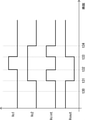
図4は、本実施の形態にかかる電源回路1における、基準電圧Vrefに使用される2種類の基準電圧Vref1,Vref2の設定値と、出力電圧Voutと、の関係を示す図である。なお、図4には、比較のため、基準電圧Vrefに使用される電圧が1種類の場合における出力電圧Voutも示されている。
FIG. 4 is a diagram showing the relationship between the set values of the two types of reference voltages Vref1 and Vref2 used for the reference voltage Vref and the output voltage Vout in the
なお、図4の例では、基準電圧Vrefに使用される電圧が1種類の場合、基準電圧Vrefは0.80Vを示すものとする。また、基準電圧Vrefに使用される電圧が基準電圧Vref1,Vref2の2種類の場合、基準電圧Vref1,Vref2の平均電圧が0.80Vを示すものとする。 In the example of FIG. 4, when one type of voltage is used for the reference voltage Vref, the reference voltage Vref is assumed to be 0.80V. Further, when there are two types of reference voltages Vref1 and Vref2, the average voltage of the reference voltages Vref1 and Vref2 is assumed to be 0.80V.
図4を参照すると、基準電圧Vrefに使用される電圧が1種類の場合、出力電圧Voutの最小値は6.93V、最大値は7.84V、平均値は7.43V、最大値と最小値の差(即ち、リップル成分)は0.91Vを示している。 Referring to FIG. 4, when one type of voltage is used for the reference voltage Vref, the minimum value of the output voltage Vout is 6.93V, the maximum value is 7.84V, the average value is 7.43V, and the maximum value and the minimum value are used. The difference (that is, the ripple component) is 0.91V.
それに対し、基準電圧Vrefに使用される電圧が、0.79Vの基準電圧Vref1、及び、0.82Vの基準電圧Vref2の2種類の場合、出力電圧Voutの最小値は7.16V、最大値は7.75V、平均値は7.47V、最大値と最小値の差(即ち、リップル成分)は0.59Vを示している。この場合、リップル成分は、基準電圧Vrefに使用される電圧が1種類の場合と比較して、約35%抑制されている。 On the other hand, when the voltage used for the reference voltage Vref is 0.79V reference voltage Vref1 and 0.82V reference voltage Vref2, the minimum value of the output voltage Vout is 7.16V and the maximum value is 7.16V. The average value is 7.75V, the average value is 7.47V, and the difference between the maximum value and the minimum value (that is, the ripple component) is 0.59V. In this case, the ripple component is suppressed by about 35% as compared with the case where the voltage used for the reference voltage Vref is one type.
また、基準電圧Vrefに使用される電圧が、0.78Vの基準電圧Vref1、及び、0.82Vの基準電圧Vref2の2種類の場合、出力電圧Voutの最小値は7.26V、最大値は7.80V、平均値は7.57V、最大値と最小値の差(即ち、リップル成分)は0.54Vを示している。この場合、リップル成分は、基準電圧Vrefに使用される電圧が1種類の場合と比較して、約41%抑制されている。 When the reference voltage Vref has two types, a reference voltage Vref1 of 0.78V and a reference voltage Vref2 of 0.82V, the minimum value of the output voltage Vout is 7.26V and the maximum value is 7. The average value is .80V, the average value is 7.57V, and the difference between the maximum value and the minimum value (that is, the ripple component) is 0.54V. In this case, the ripple component is suppressed by about 41% as compared with the case where the voltage used for the reference voltage Vref is one type.
図5は、本実施の形態にかかる電源回路における、出力端子OUTに付加される安定化容量の容量値と、出力電圧Voutと、の関係を示す図である。なお、図5には、比較のため、基準電圧Vrefに使用される電圧が1種類の場合における出力電圧Voutも示されている。 FIG. 5 is a diagram showing the relationship between the capacitance value of the stabilized capacitance added to the output terminal OUT and the output voltage Vout in the power supply circuit according to the present embodiment. Note that FIG. 5 also shows the output voltage Vout when one type of voltage is used for the reference voltage Vref for comparison.
なお、図5の例では、基準電圧Vrefに使用される電圧が1種類の場合、基準電圧Vrefが0.80Vを示し、かつ、安定化容量が16pFを示すものとする。また、基準電圧Vrefに使用される電圧が基準電圧Vref1,Vref2の2種類の場合、基準電圧Vref1が0.78V、基準電圧Vref2が0.82Vを示すものとする。 In the example of FIG. 5, when one kind of voltage is used for the reference voltage Vref, it is assumed that the reference voltage Vref shows 0.80V and the stabilized capacitance shows 16pF. When the reference voltage Vref has two types of voltages, the reference voltage Vref1 and the reference voltage Vref2, the reference voltage Vref1 indicates 0.78V and the reference voltage Vref2 indicates 0.82V.
図5を参照すると、基準電圧Vrefに使用される電圧が1種類、かつ、安定化容量が16pFの場合、出力電圧Voutの最小値は6.93V、最大値は7.84V、平均値は7.43V、最大値と最小値の差(即ち、リップル成分)は0.91Vを示している。 Referring to FIG. 5, when one type of voltage is used for the reference voltage Vref and the stabilized capacitance is 16 pF, the minimum value of the output voltage Vout is 6.93 V, the maximum value is 7.84 V, and the average value is 7. It shows .43V, and the difference between the maximum value and the minimum value (that is, the ripple component) is 0.91V.
それに対し、基準電圧Vrefに使用される電圧が2種類、かつ、安定化容量が16pFの場合、出力電圧Voutの最小値は7.26V、最大値は7.80V、平均値は7.57V、最大値と最小値の差(即ち、リップル成分)は0.54Vを示している。この場合、リップル成分は、既に説明したように、基準電圧Vrefに使用される電圧が1種類の場合と比較して、約41%抑制されている。 On the other hand, when there are two types of voltages used for the reference voltage Vref and the stabilized capacitance is 16 pF, the minimum value of the output voltage Vout is 7.26 V, the maximum value is 7.80 V, and the average value is 7.57 V. The difference between the maximum value and the minimum value (that is, the ripple component) shows 0.54V. In this case, as described above, the ripple component is suppressed by about 41% as compared with the case where the voltage used for the reference voltage Vref is one type.
ここで、安定化容量の容量値を8pFまで小さくすると、出力電圧Voutの最小値は7.01V、最大値は7.83V、平均値は7.52V、最大値と最小値の差(即ち、リップル成分)は0.82Vを示す。さらに、安定化容量の容量値を6pFまで小さくすると、出力電圧Voutの最小値は6.88V、最大値は7.95V、平均値は7.50V、最大値と最小値の差(即ち、リップル成分)は1.07Vを示す。したがって、安定化容量の容量値が7pF程度の場合に、出力電圧Voutのリップル成分が0.9V程度になるものと考えられる。 Here, when the capacitance value of the stabilized capacitance is reduced to 8 pF, the minimum value of the output voltage Vout is 7.01 V, the maximum value is 7.83 V, the average value is 7.52 V, and the difference between the maximum value and the minimum value (that is, that is). Ripple component) shows 0.82V. Further, when the capacitance value of the stabilized capacitance is reduced to 6 pF, the minimum value of the output voltage Vout is 6.88 V, the maximum value is 7.95 V, the average value is 7.50 V, and the difference between the maximum value and the minimum value (that is, ripple). Component) shows 1.07V. Therefore, when the capacitance value of the stabilized capacitance is about 7 pF, it is considered that the ripple component of the output voltage Vout is about 0.9 V.
つまり、基準電圧Vrefに使用される電圧が2種類の場合には、安定化容量の容量値を7pF程度にまで小さくしても、基準電圧Vrefに使用される電圧が1種類の場合、かつ、安定化容量が16pFの場合と同等程度のリップル成分に抑えることができる。換言すると、本実施の形態にかかる電源回路11は、基準電圧Vrefに使用される電圧が1種類の場合と比較して、より小さな回路規模で同等のリップル成分の抑制を実現することができる。
That is, when there are two types of voltages used for the reference voltage Vref, even if the capacitance value of the stabilized capacitance is reduced to about 7 pF, there is only one type of voltage used for the reference voltage Vref, and The ripple component can be suppressed to the same level as when the stabilized capacitance is 16 pF. In other words, the
(電源回路1の変形例)
図6は、電源回路1の変形例を電源回路1aとして示す図である。
電源回路1aは、電源回路1と比較して、論理和回路(以下、OR回路と称す)15をさらに備える。
(Modification example of power supply circuit 1)
FIG. 6 is a diagram showing a modified example of the
The
OR回路15は、所謂イネーブル回路であって、外部から供給されたイネーブル信号ENと、コンパレータ13から出力された電圧Vcと、の論理和を、電圧Vselとして出力する。なお、イネーブル信号ENは、例えば、昇圧回路11又はその周辺回路の動作の可否を制御するために用いられているイネーブル信号と共用されても良い。
The OR
OR回路15は、イネーブル信号ENがHレベルの場合、コンパレータ13の出力電圧Vcに関わらずHレベルの電圧Vselを出力し、イネーブル信号ENがLレベルの場合、コンパレータ13の出力電圧Vcをそのまま電圧Vselとして出力する。この電圧Vselは、電圧Vcの代わりに、選択回路12及びNAND回路14に入力される。
When the enable signal EN is H level, the
例えば、電源起動直後の所定期間、イネーブル信号ENはHレベルに設定される。それにより、コンパレータ13の出力電圧Vcが不安定な場合でも、選択回路12及びNAND回路14に入力される電圧Vselを安定したレベル(Hレベル)に固定することができる。そして、所定期間経過後、コンパレータ13の出力電圧Vcが安定すると、イネーブル信号ENはHレベルからLレベルに切り替わる。それにより、安定したコンパレータ13の出力電圧Vcを、電圧Vselとして、選択回路12及びNAND回路14に入力することができる。
For example, the enable signal EN is set to the H level for a predetermined period immediately after the power is turned on. As a result, even when the output voltage Vc of the
なお、OR回路15は、イネーブル信号ENに基づいてコンパレータ13の出力電圧Vc及び固定電圧の何れかを電圧Vselとして出力することが可能な他の回路に適宜変更可能である。
The OR
<実施の形態2>
図7は、実施の形態2にかかる電源回路2の構成例を示す図である。電源回路2は、電源回路1と比較して、選択回路12の代わりに選択回路21を備える。また、電源回路2には、基準電圧Vref1,Vref2が供給される代わりに基準電圧Vrefのみが供給されている。さらに、抵抗素子R1は、抵抗素子R1a,R1bの代わりに、抵抗素子R1c,R1d,R1eによって構成されている。以下、具体的に説明する。
<
FIG. 7 is a diagram showing a configuration example of the
図7に示すように、電源回路2は、昇圧回路11と、選択回路21と、コンパレータ13と、NAND回路14と、抵抗素子R1と、を備える。
As shown in FIG. 7, the
抵抗素子R1は、抵抗素子R1c,R1d,R1eによって構成され、電源回路2の出力端子OUTと、接地電圧端子GNDと、の間に直列に設けられている。抵抗素子R1は、抵抗素子R1c,R1d間のノードN1の電圧Vd1を出力するとともに、抵抗素子R1d,R1e間のノードN2の電圧Vd2を出力する。換言すると、抵抗素子R1は、電源回路2の出力端子OUTの電圧Voutを、抵抗素子R1cと抵抗素子R1d,R1eとの抵抗比で分圧して電圧Vd1として出力するとともに、抵抗素子R1c,R1dと抵抗素子R1eとの抵抗比で分圧して電圧Vd2として出力する。
The resistance element R1 is composed of resistance elements R1c, R1d, and R1e, and is provided in series between the output terminal OUT of the
選択回路21は、コンパレータ13から出力される電圧Vcに基づいて、分圧電圧Vd1及び分圧電圧Vd2の何れかを選択して分圧電圧Vdとして出力する。なお、本実施の形態では、分圧電圧Vd1が分圧電圧Vd2よりも大きい場合を例に説明する。
The
例えば、コンパレータ13からLレベルの電圧Vcが出力されている場合、選択回路21は、分圧電圧Vd2を選択して分圧電圧Vdとして出力する。それに対し、コンパレータ13からHレベルの電圧Vcが出力されている場合、選択回路21は、分圧電圧Vd1を選択して分圧電圧Vdとして出力する。
For example, when the L level voltage Vc is output from the
電源回路2のその他の構成については、電源回路1の場合と同様であるため、その説明を省略する。
Since the other configurations of the
(電源回路2の動作)
続いて、図8を用いて、電源回路2の動作について説明する。
図8は、電源回路2の動作を示すタイミングチャートである。なお、以下では、昇圧回路11を駆動する電源電圧VDDが2V、昇圧回路11の出力電圧Voutのターゲット電圧が10V、抵抗素子R1c,R1d,R1eの抵抗比R1c:R1d:R1eが8.95:0.1:0.95、基準電圧Vrefが1Vである場合を例に説明する。
(Operation of power supply circuit 2)
Subsequently, the operation of the
FIG. 8 is a timing chart showing the operation of the
図8に示すように、昇圧回路11による出力電圧Voutの昇圧開始直後は、出力電圧Voutは、電源電圧VDD(=2V)以上、かつ、ターゲット電圧(=10V)以下を示している(時刻t20)。例えば、出力電圧Voutが5Vを示す場合、分圧電圧Vd1は0.525Vを示し、分圧電圧Vd2は0.475Vを示す。このとき、基準電圧Vref(=1V)は、選択回路21によって分圧電圧Vd1,Vd2のうち何れが分圧電圧Vdとして選択されているかに関わらず、分圧電圧Vdよりも大きくなる。そのため、コンパレータ13は、Hレベルの電圧Vcを出力する。
As shown in FIG. 8, immediately after the start of boosting of the output voltage Vout by the
コンパレータ13からHレベルの電圧Vcが出力されている場合、選択回路21は、分圧電圧Vd1(=0.525V)を選択して分圧電圧Vdとして出力する。また、このとき、NAND回路14は、昇圧回路11へのクロック信号CLKの供給を行う。それにより、昇圧回路11は、出力電圧Voutの昇圧を継続する。
When the H level voltage Vc is output from the
出力電圧Voutが上昇すると、それに伴って、出力電圧Voutの分圧電圧Vd(ここでは、Vd=Vd1)も上昇する。したがって、しばらくすると、分圧電圧Vdは、基準電圧Vref(=1V)に達する(時刻t21)。しかしながら、コンパレータ13は、コンパレータ13のオフセット電圧、コンパレータ13の反応速度、及び、昇圧回路11によって決まる出力電圧Voutの昇圧速度などの影響を受けて、出力電圧VcをHレベルに維持する。
As the output voltage Vout rises, the voltage divider voltage Vd (here, Vd = Vd1) of the output voltage Vout also rises accordingly. Therefore, after a while, the voltage dividing voltage Vd reaches the reference voltage Vref (= 1V) (time t21). However, the
その後、出力電圧Voutがさらに上昇し、それに伴って、分圧電圧Vdが上昇すると、コンパレータ13は、出力電圧VcをHレベルからLレベルに切り替える(時刻t22)。例えば、出力電圧Voutがターゲット電圧(=10V)を超えて11Vを示す場合、分圧電圧Vd1は1.155Vを示し、分圧電圧Vd2は1.045Vを示す。このとき、分圧電圧Vd(=1.155V)は、基準電圧Vref(=1V)よりも大きくなるため、コンパレータ13は、Lレベルの電圧Vcを出力する。
After that, when the output voltage Vout further rises and the voltage dividing voltage Vd rises accordingly, the
それにより、選択回路21は、分圧電圧Vd1から分圧電圧Vd2に選択を切り替えて分圧電圧Vdとして出力する。また、このとき、NAND回路14は、昇圧回路11へのクロック信号CLKの供給を停止させる。それにより、昇圧回路11は、出力電圧Voutの昇圧を停止させる。それにより、出力電圧Voutは、下降し始める。
As a result, the
出力電圧Voutが下降すると、それに伴って、出力電圧Voutの分圧電圧Vd(ここでは、Vd=Vd2)も下降する。したがって、しばらくすると、分圧電圧Vdは、基準電圧Vref(=1V)に達する(時刻t23)。しかしながら、コンパレータ13は、コンパレータ13のオフセット電圧、コンパレータ13の反応速度、及び、昇圧回路11の出力電流負荷によって決まる出力電圧Voutの下降速度などの影響を受けて、出力電圧VcをLレベルに維持する。
When the output voltage Vout decreases, the voltage dividing voltage Vd (here, Vd = Vd2) of the output voltage Vout also decreases accordingly. Therefore, after a while, the voltage dividing voltage Vd reaches the reference voltage Vref (= 1V) (time t23). However, the
その後、出力電圧Voutがさらに下降し、それに伴って、分圧電圧Vdが下降すると、コンパレータ13は、出力電圧VcをLレベルからHレベルに切り替える(時刻t24)。それにより、選択回路21は、分圧電圧Vd2から分圧電圧Vd1に選択を切り替えて分圧電圧Vdとして出力する。また、このとき、NAND回路14は、昇圧回路11へのクロック信号CLKの供給を再開させる。それにより、昇圧回路11は、出力電圧Voutの昇圧を再開させる。
After that, when the output voltage Vout further decreases and the voltage dividing voltage Vd decreases accordingly, the
その後、時刻t25以降では、時刻t21~t25の動作が繰り返される。 After that, after the time t25, the operations of the times t21 to t25 are repeated.
このように、本実施の形態にかかる電源回路2は、基準電圧Vrefと、選択的に用いられる分圧電圧Vd1,Vd2の何れかと、の比較結果に基づいて、昇圧回路11による出力電圧Voutの昇圧の可否を制御している。それにより、本実施の形態にかかる電源回路2は、昇圧回路11のリップル上昇成分及びリップル下降成分を部分的に重複させることができるため、昇圧回路11の全体的なリップル成分を抑制することができる。換言すると、本実施の形態にかかる電源回路1は、負荷への出力電流の大きさに関係なく、安定した出力電圧Voutを生成することができる。
As described above, the
(電源回路2の変形例)
図9は、電源回路2の変形例を電源回路2aとして示す図である。
電源回路2aは、電源回路2と比較して、論理和回路(以下、OR回路と称す)22をさらに備える。
(Modification example of power supply circuit 2)
FIG. 9 is a diagram showing a modified example of the
The
OR回路22は、所謂イネーブル回路であって、外部から供給されたイネーブル信号ENと、コンパレータ13から出力された電圧Vcと、の論理和を、電圧Vselとして出力する。なお、イネーブル信号ENは、例えば、昇圧回路11又はその周辺回路の動作の可否を制御するために用いられているイネーブル信号と共用されても良い。
The OR
OR回路22は、イネーブル信号ENがHレベルの場合、コンパレータ13の出力電圧Vcに関わらずHレベルの電圧Vselを出力し、イネーブル信号ENがLレベルの場合、コンパレータ13の出力電圧Vcをそのまま電圧Vselとして出力する。この電圧Vselは、電圧Vcの代わりに、選択回路21及びNAND回路14に入力される。
When the enable signal EN is H level, the
例えば、電源起動直後の所定期間、イネーブル信号ENはHレベルに設定される。それにより、コンパレータ13の出力電圧Vcが不安定な場合でも、選択回路21及びNAND回路14に入力される電圧Vselのレベルを安定させることができる。そして、所定期間経過後、コンパレータ13の出力電圧Vcが安定すると、イネーブル信号ENはHレベルからLレベルに切り替わる。それにより、安定したコンパレータ13の出力電圧Vcを、電圧Vselとして、選択回路21及びNAND回路14に入力することができる。
For example, the enable signal EN is set to the H level for a predetermined period immediately after the power is turned on. As a result, even when the output voltage Vc of the
なお、OR回路22は、イネーブル信号ENに基づいてコンパレータ13の出力電圧Vc及び固定電圧の何れかを電圧Vselとして出力することが可能な他の回路に適宜変更可能である。
The OR
<実施の形態3>
図10は、実施の形態3にかかる電源回路3の構成例を示す図である。電源回路3は、電源回路1と比較して、比較部10の代わりに比較部30を備える。比較部30は、コンパレータ31と、コンパレータ32と、制御回路33と、を有する。
<
FIG. 10 is a diagram showing a configuration example of the
コンパレータ31は、分圧電圧Vdと基準電圧Vref1とを比較して、比較結果である電圧Vc1を出力する。理想的には、コンパレータ31は、分圧電圧Vdが基準電圧Vref1以上の場合にHレベルの電圧Vc1を出力し、分圧電圧Vdが基準電圧Vref1未満の場合にLレベルの電圧Vc1を出力する。
The
コンパレータ32は、分圧電圧Vdと基準電圧Vref2とを比較して、比較結果である電圧Vc2を出力する。理想的には、コンパレータ32は、分圧電圧Vdが基準電圧Vref2以上の場合にHレベルの電圧Vc2を出力し、分圧電圧Vdが基準電圧Vref2未満の場合にLレベルの電圧Vc2を出力する。
The
制御回路33は、コンパレータ31,32のそれぞれから出力された電圧Vc1,Vc2に応じた電圧Vcoutを出力する。
The
(制御回路33の具体的な構成例)
図11は、制御回路33の具体的な構成例を示す図である。
図11に示すように、制御回路33は、排他的論理和回路(XOR回路)331と、Dフリップフロップ332と、を備える。
(Specific configuration example of the control circuit 33)
FIG. 11 is a diagram showing a specific configuration example of the
As shown in FIG. 11, the
XOR回路331は、電圧Vc1,Vc2の排他的論理和を、電圧Vcintとして出力する。Dフリップフロップ332は、電圧Vcintの立ち上がりに同期して電圧Voutを取り込み、論理反転させて電圧Voutとして出力する。
The
なお、制御回路33の構成は、図11に示す構成に限られず、図11に示す構成と同等の機能を実現可能な他の構成に適宜変更可能である。
The configuration of the
図10に戻り、説明を続ける。
NAND回路14は、制御回路33の出力電圧Vcoutに基づいて、昇圧回路11に対してクロック信号CLKを出力するか否かを制御する。例えば、制御回路33からLレベルの信号が出力されている場合、NAND回路14は、クロック信号CLKに関わらずHレベルの信号を出力する。つまり、NAND回路14は、昇圧回路11へのクロック信号CLKの供給を停止させる。それに対し、コンパレータ13からHレベルの信号が出力されている場合、NAND回路14は、昇圧回路11へのクロック信号CLK(厳密に言えば、本例ではクロック信号CLKの反転信号)の供給を行う。このとき、昇圧回路11は、出力Voutを昇圧させる。
Returning to FIG. 10, the description will be continued.
The
電源回路3のその他の構成については、電源回路1の場合と同様であるため、その説明を省略する。
Since the other configurations of the
(電源回路3の動作)
続いて、図12を用いて、電源回路3の動作について説明する。
図12は、電源回路3の動作を示すタイミングチャートである。なお、以下では、昇圧回路11を駆動する電源電圧VDDが2V、昇圧回路11の出力電圧Voutのターゲット電圧が10V、抵抗素子R1a,R1bの抵抗比R1a:R1bが9:1、基準電圧Vref1が1.05V、基準電圧Vref2が0.95Vである場合を例に説明する。
(Operation of power supply circuit 3)
Subsequently, the operation of the
FIG. 12 is a timing chart showing the operation of the
図12に示すように、昇圧回路11による出力電圧Voutの昇圧開始直後は、出力電圧Voutは、ターゲット電圧(=10V)に満たない状態である(時刻t30)。そのため、コンパレータ31,32は何れもLレベルの電圧Vc1,Vc2を出力する。このとき、制御回路33では、XOR回路331がLレベルの電圧Vcintを出力するため、Dフリップフロップ332は、初期値であるHレベルの電圧Vcoutを出力する。
As shown in FIG. 12, immediately after the start of boosting of the output voltage Vout by the
制御回路33からHレベルの電圧Vcoutが出力されるため、NAND回路14は、昇圧回路11へのクロック信号CLKの供給を行う。それにより、昇圧回路11は、出力電圧Voutの昇圧を継続する。
Since the H level voltage Vcout is output from the
その後、出力電圧Voutが上昇してターゲット電圧を超えると、まず、コンパレータ32の出力電圧Vc2がLレベルからHレベルに切り替わり(時刻t31)、その後、コンパレータ31の出力電圧Vc1がLレベルからHレベルに切り替わる(時刻t32)。それにより、制御回路33では、XOR回路331の出力電圧VcintがLレベルからHレベルに切り替わり(時刻t31)、その後、HレベルからLレベルに切り替わる(時刻t32)。このとき、Dフリップフロップ332は、XOR回路331の出力電圧Vcintの立ち上がりに同期して出力電圧VoutをHレベルからLレベルに反転させる(時刻t31)。
After that, when the output voltage Vout rises and exceeds the target voltage, the output voltage Vc2 of the
制御回路33からLレベルの電圧Vcoutが出力されるため、NAND回路14は、昇圧回路11へのクロック信号CLKの供給を停止させる。それにより、昇圧回路11は、出力電圧Voutの昇圧を停止させる。それにより、出力電圧Voutは、下降し始める。
Since the L level voltage Vcout is output from the
その後、出力電圧Voutが下降してターゲット電圧を下回ると、まず、コンパレータ31の出力電圧Vc1がHレベルからLレベルに切り替わり(時刻t33)、その後、コンパレータ32の出力電圧Vc2がHレベルからLレベルに切り替わる(時刻t34)。それにより、制御回路33では、XOR回路331の出力電圧VcintがLレベルからHレベルに切り替わり(時刻t33)、その後、HレベルからLレベルに切り替わる(時刻t34)。このとき、Dフリップフロップ332は、XOR回路331の出力電圧Vcintの立ち上がりに同期して出力電圧VoutをLレベルからHレベルに反転させる(時刻t34)。
After that, when the output voltage Vout drops and falls below the target voltage, the output voltage Vc1 of the
その後は、時刻t31~t34の動作が繰り返される。 After that, the operations at times t31 to t34 are repeated.
このように、本実施の形態にかかる電源回路3は、出力電圧Voutの分圧電圧Vdと、基準電圧Vref1,Vref2のそれぞれと、の比較結果に基づいて、昇圧回路11による出力電圧Voutの昇圧の可否を制御している。それにより、本実施の形態にかかる電源回路3は、昇圧回路11のリップル上昇成分及びリップル下降成分を部分的に重複させることができるため、昇圧回路11の全体的なリップル成分を抑制することができる。換言すると、本実施の形態にかかる電源回路1は、負荷への出力電流の大きさに関係なく、安定した出力電圧Voutを生成することができる。
As described above, in the
(電源回路3の変形例)
図13は、電源回路3の変形例を電源回路3aとして示す図である。電源回路3aは、電源回路3と比較して、論理和回路(以下、OR回路と称す)34をさらに備える。
(Modification example of power supply circuit 3)
FIG. 13 is a diagram showing a modified example of the
OR回路34は、所謂イネーブル回路であって、外部から供給されたイネーブル信号ENと、制御回路33から出力された電圧Vcoutと、の論理和を、電圧Vselとして出力する。なお、イネーブル信号ENは、例えば、昇圧回路11又はその周辺回路の動作の可否を制御するために用いられているイネーブル信号と共用されても良い。
The OR
OR回路34は、イネーブル信号ENがHレベルの場合、制御回路33の出力電圧Vcoutに関わらずHレベルの電圧Vselを出力し、イネーブル信号ENがLレベルの場合、制御回路33の出力電圧Vcoutをそのまま電圧Vselとして出力する。この電圧Vselは、電圧Vcoutの代わりに、NAND回路14に入力される。
When the enable signal EN is H level, the
例えば、電源起動直後の所定期間、イネーブル信号ENはHレベルに設定される。それにより、制御回路33の出力電圧Vcoutが不安定な場合でも、NAND回路14に入力される電圧Vselのレベルを安定させることができる。そして、所定期間経過後、制御回路33の出力電圧Vcoutが安定すると、イネーブル信号ENはHレベルからLレベルに切り替わる。それにより、安定した制御回路33の出力電圧Vcoutを、電圧Vselとして、NAND回路14に入力することができる。
For example, the enable signal EN is set to the H level for a predetermined period immediately after the power is turned on. As a result, even when the output voltage Vcout of the
なお、OR回路34は、イネーブル信号ENに基づいて制御回路33の出力電圧Vcout及び固定電圧の何れかを電圧Vselとして出力することが可能な他の回路に適宜変更可能である。
The OR
以上、本発明者によってなされた発明を実施の形態に基づき具体的に説明したが、本発明は既に述べた実施の形態に限定されるものではなく、その要旨を逸脱しない範囲において種々の変更が可能であることはいうまでもない。 Although the invention made by the present inventor has been specifically described above based on the embodiments, the present invention is not limited to the embodiments already described, and various changes can be made without departing from the gist thereof. It goes without saying that it is possible.
上記実施の形態1~3では、基準電圧Vref1,Vref2の値が固定されているか、または、分圧電圧Vd1,Vd2の値が固定されている場合について説明したが、これに限られない。上記実施の形態1~3に係る電源回路1~3は、例えば、出力電圧Voutのリップル成分(変動幅)を測定する測定回路と、測定回路による測定結果に基づいて基準電圧Vref1,Vref2又は分圧電圧Vd1,Vd2の値を調整する調整回路と、を備えていても良い。それにより、出力電圧Voutのリップル成分をさらに抑制することが可能となる。
In the
例えば、上記の実施の形態に係る電源回路では、半導体基板、半導体層、拡散層(拡散領域)などの導電型(p型もしくはn型)を反転させた構成としてもよい。そのため、n型、及びp型の一方の導電型を第1の導電型とし、他方の導電型を第2の導電型とした場合、第1の導電型をp型、第2の導電型をn型とすることもできるし、反対に第1の導電型をn型、第2の導電型をp型とすることもできる。 For example, in the power supply circuit according to the above embodiment, the conductive type (p type or n type) such as the semiconductor substrate, the semiconductor layer, and the diffusion layer (diffusion region) may be inverted. Therefore, when one of the n-type and the p-type is the first conductive type and the other conductive type is the second conductive type, the first conductive type is the p-type and the second conductive type is the second conductive type. It can be n-type, or conversely, the first conductive type can be n-type and the second conductive type can be p-type.
1~3 電源回路
1a 電源回路
2a 電源回路
3a 電源回路
10 比較部
11 昇圧回路
12 選択回路
13 コンパレータ
14 否定論理積回路(NAND回路)
15 論理和回路(OR回路)
21 選択回路
22 論理和回路(OR回路)
30 比較部
31 コンパレータ
32 コンパレータ
33 制御回路
34 論理和回路(OR回路)
331 排他的論理和回路(XOR回路)
332 Dフリップフロップ
INV1 インバータ
MN1,MN2 NチャネルMOSトランジスタ
MP1,MP2 PチャネルMOSトランジスタ
N0,N1,N2 ノード
R1 抵抗素子
R1a,R1b,R1c,R1d,R1e 抵抗素子
TG1 トランスファゲート
TG2 トランスファゲート
1-3
15 OR circuit (OR circuit)
21
30
331 Exclusive OR circuit (XOR circuit)
332 D flip-flop INV1 inverter MN1, MN2 N-channel MOS transistor MP1, MP2 P-channel MOS transistor N0, N1, N2 node R1 resistance element R1a, R1b, R1c, R1d, R1e resistance element TG1 transfer gate TG2 transfer
Claims (6)
前記比較部による比較結果に基づいてクロック信号の出力の可否を制御する第1イネーブル回路と、
前記クロック信号が前記第1イネーブル回路を介して供給された場合に、前記外部出力電圧を昇圧する昇圧回路と、
を備え、
前記比較部は、
前記分圧電圧と、前記第1及び第2基準電圧のうち選択された何れかの基準電圧と、を比較して、前記比較部による比較結果として出力するコンパレータと、
前記コンパレータによる比較結果に基づいて、前記第1基準電圧及び前記第2基準電圧の何れかを選択し、前記選択された基準電圧として出力する選択回路と、
を有し、
前記選択回路は、前記分圧電圧が前記選択された基準電圧以上であることを示す比較結果が前記コンパレータから出力された場合に、前記第2基準電圧から前記第2基準電圧よりも高い前記第1基準電圧に選択を切り替えて、前記選択された基準電圧として出力し、かつ、前記分圧電圧が前記選択された基準電圧未満であることを示す比較結果が前記コンパレータから出力された場合に、前記第1基準電圧から前記第2基準電圧に選択を切り替えて、前記選択された基準電圧として出力する、
電源回路。 A comparison unit that compares the divided voltage according to the external output voltage with each of the first reference voltage and the second reference voltage and outputs the comparison result.
The first enable circuit that controls whether or not the clock signal can be output based on the comparison result by the comparison unit, and
A booster circuit that boosts the external output voltage when the clock signal is supplied via the first enable circuit, and a booster circuit.
Equipped with
The comparison unit
A comparator that compares the divided voltage with a reference voltage selected from the first and second reference voltages and outputs the comparison result by the comparison unit.
A selection circuit that selects either the first reference voltage or the second reference voltage based on the comparison result by the comparator and outputs the selected reference voltage.
Have,
The selection circuit has the second reference voltage higher than the second reference voltage when a comparison result indicating that the voltage dividing voltage is equal to or higher than the selected reference voltage is output from the comparator. 1 When the selection is switched to the reference voltage, the voltage is output as the selected reference voltage, and the comparison result indicating that the divided voltage is less than the selected reference voltage is output from the comparator. The selection is switched from the first reference voltage to the second reference voltage, and the voltage is output as the selected reference voltage.
Power circuit.
前記比較部による比較結果に基づいてクロック信号の出力の可否を制御する第1イネーブル回路と、
前記クロック信号が前記第1イネーブル回路を介して供給された場合に、前記外部出力電圧を昇圧する昇圧回路と、
前記外部出力電圧の変動幅を測定する測定回路と、
前記測定回路による測定結果に基づいて、前記第1基準電圧及び前記第2基準電圧の値を調整する調整回路と、
を備え、
前記比較部は、
前記分圧電圧と、前記第1及び第2基準電圧のうち選択された何れかの基準電圧と、を比較して、前記比較部による比較結果として出力するコンパレータと、
前記コンパレータによる比較結果に基づいて、前記第1基準電圧及び前記第2基準電圧の何れかを選択し、前記選択された基準電圧として出力する選択回路と、
を有する、
電源回路。 A comparison unit that compares the divided voltage according to the external output voltage with each of the first reference voltage and the second reference voltage and outputs the comparison result.
The first enable circuit that controls whether or not the clock signal can be output based on the comparison result by the comparison unit, and
A booster circuit that boosts the external output voltage when the clock signal is supplied via the first enable circuit, and a booster circuit.
A measurement circuit that measures the fluctuation range of the external output voltage,
An adjustment circuit that adjusts the values of the first reference voltage and the second reference voltage based on the measurement results of the measurement circuit, and
Equipped with
The comparison unit
A comparator that compares the divided voltage with a reference voltage selected from the first and second reference voltages and outputs the comparison result by the comparison unit.
A selection circuit that selects either the first reference voltage or the second reference voltage based on the comparison result by the comparator and outputs the selected reference voltage.
Have,
Power circuit.
前記比較部による比較結果に基づいてクロック信号の出力の可否を制御する第1イネーブル回路と、
前記クロック信号が前記第1イネーブル回路を介して供給された場合に、前記外部出力電圧を昇圧する昇圧回路と、
を備え、
前記比較部は、
前記分圧電圧と、前記第1基準電圧と、を比較する第1コンパレータと、
前記分圧電圧と、前記第2基準電圧と、を比較する第2コンパレータと、
前記第1コンパレータ及び前記第2コンパレータのそれぞれの比較結果に応じた電圧を、前記比較部による比較結果として出力する制御回路と、
を有し、
前記制御回路は、
前記第1コンパレータによる比較結果と、前記第2コンパレータによる比較結果と、の排他的論理和を出力する排他的論理和回路と、
前記排他的論理和回路の出力電圧の立ち上がりに同期して、前記制御回路の出力電圧を反転させるフリップフロップ回路と、
を有する、
電源回路。 A comparison unit that compares the divided voltage according to the external output voltage with each of the first reference voltage and the second reference voltage and outputs the comparison result.
The first enable circuit that controls whether or not the clock signal can be output based on the comparison result by the comparison unit, and
A booster circuit that boosts the external output voltage when the clock signal is supplied via the first enable circuit, and a booster circuit.
Equipped with
The comparison unit
A first comparator that compares the voltage divider voltage with the first reference voltage,
A second comparator that compares the voltage divider voltage with the second reference voltage,
A control circuit that outputs a voltage corresponding to each comparison result of the first comparator and the second comparator as a comparison result by the comparison unit, and a control circuit.
Have,
The control circuit is
An exclusive OR circuit that outputs an exclusive OR of the comparison result by the first comparator and the comparison result by the second comparator.
A flip-flop circuit that inverts the output voltage of the control circuit in synchronization with the rise of the output voltage of the exclusive OR circuit.
Have,
Power circuit.
前記比較部による比較結果に基づいてクロック信号の出力の可否を制御する第1イネーブル回路と、
前記クロック信号が前記第1イネーブル回路を介して供給された場合に、前記外部出力電圧を昇圧する昇圧回路と、
前記外部出力電圧の変動幅を測定する測定回路と、
前記測定回路による測定結果に基づいて、前記第1基準電圧及び前記第2基準電圧の値を調整する調整回路と、
を備え、
前記比較部は、
前記分圧電圧と、前記第1基準電圧と、を比較する第1コンパレータと、
前記分圧電圧と、前記第2基準電圧と、を比較する第2コンパレータと、
前記第1コンパレータ及び前記第2コンパレータのそれぞれの比較結果に応じた電圧を、前記比較部による比較結果として出力する制御回路と、
を有する、
電源回路。 A comparison unit that compares the divided voltage according to the external output voltage with each of the first reference voltage and the second reference voltage and outputs the comparison result.
The first enable circuit that controls whether or not the clock signal can be output based on the comparison result by the comparison unit, and
A booster circuit that boosts the external output voltage when the clock signal is supplied via the first enable circuit, and a booster circuit.
A measurement circuit that measures the fluctuation range of the external output voltage,
An adjustment circuit that adjusts the values of the first reference voltage and the second reference voltage based on the measurement results of the measurement circuit, and
Equipped with
The comparison unit
A first comparator that compares the voltage divider voltage with the first reference voltage,
A second comparator that compares the voltage divider voltage with the second reference voltage,
A control circuit that outputs a voltage corresponding to each comparison result of the first comparator and the second comparator as a comparison result by the comparison unit, and a control circuit.
Have,
Power circuit.
前記コンパレータによる比較結果に基づいて、前記第1分圧電圧及び前記第2分圧電圧の何れかを選択し、前記選択された分圧電圧として出力する選択回路と、
前記コンパレータによる比較結果に基づいてクロック信号の出力の可否を制御する第1イネーブル回路と、
前記クロック信号が前記第1イネーブル回路を介して供給された場合に、前記外部出力電圧を昇圧する昇圧回路と、
を備え、
前記選択回路は、前記選択された分圧電圧が前記基準電圧以上であることを示す比較結果が前記コンパレータから出力された場合に、第1分圧電圧から前記第1分圧電圧よりも低い前記第2分圧電圧に選択を切り替えて、前記選択された分圧電圧として出力し、かつ、前記選択された分圧電圧が前記基準電圧未満であることを示す比較結果が前記コンパレータから出力された場合に、前記第2分圧電圧から前記第1分圧電圧に選択を切り替えて、前記選択された分圧電圧として出力する、
電源回路。 A comparator that compares the voltage divider selected from the first voltage divider voltage and the second voltage divider voltage according to the external output voltage with the reference voltage.
A selection circuit that selects either the first voltage divider voltage or the second voltage divider voltage based on the comparison result by the comparator and outputs the selected voltage divider voltage.
A first enable circuit that controls whether or not a clock signal can be output based on the comparison result of the comparator, and
A booster circuit that boosts the external output voltage when the clock signal is supplied via the first enable circuit, and a booster circuit.
Equipped with
In the selection circuit, when a comparison result indicating that the selected voltage division voltage is equal to or higher than the reference voltage is output from the comparator, the first voltage division voltage is lower than the first voltage division voltage. The selector is output as a comparison result indicating that the selection is switched to the second divided voltage and the selected voltage is output as the selected divided voltage and the selected divided voltage is less than the reference voltage. In this case, the selection is switched from the second divided voltage to the first divided voltage, and the voltage is output as the selected divided voltage.
Power circuit.
前記コンパレータによる比較結果に基づいて、前記第1分圧電圧及び前記第2分圧電圧の何れかを選択し、前記選択された分圧電圧として出力する選択回路と、
前記コンパレータによる比較結果に基づいてクロック信号の出力の可否を制御する第1イネーブル回路と、
前記クロック信号が前記第1イネーブル回路を介して供給された場合に、前記外部出力電圧を昇圧する昇圧回路と、
前記外部出力電圧の変動幅を測定する測定回路と、
前記測定回路による測定結果に基づいて、前記第1分圧電圧及び前記第2分圧電圧の値を調整する調整回路と、
を備えた電源回路。 A comparator that compares the voltage divider selected from the first voltage divider voltage and the second voltage divider voltage according to the external output voltage with the reference voltage.
A selection circuit that selects either the first voltage divider voltage or the second voltage divider voltage based on the comparison result by the comparator and outputs the selected voltage divider voltage.
A first enable circuit that controls whether or not a clock signal can be output based on the comparison result of the comparator, and
A booster circuit that boosts the external output voltage when the clock signal is supplied via the first enable circuit, and a booster circuit.
A measurement circuit that measures the fluctuation range of the external output voltage,
An adjustment circuit that adjusts the values of the first voltage divider voltage and the second voltage divider voltage based on the measurement results of the measurement circuit, and
Power supply circuit with.
Priority Applications (3)
| Application Number | Priority Date | Filing Date | Title |
|---|---|---|---|
| JP2018117743A JP7003003B2 (en) | 2018-06-21 | 2018-06-21 | Power circuit |
| CN201910482325.0A CN110635681B (en) | 2018-06-21 | 2019-06-04 | power supply |
| US16/433,835 US10644580B2 (en) | 2018-06-21 | 2019-06-06 | Power supplies |
Applications Claiming Priority (1)
| Application Number | Priority Date | Filing Date | Title |
|---|---|---|---|
| JP2018117743A JP7003003B2 (en) | 2018-06-21 | 2018-06-21 | Power circuit |
Publications (2)
| Publication Number | Publication Date |
|---|---|
| JP2019221087A JP2019221087A (en) | 2019-12-26 |
| JP7003003B2 true JP7003003B2 (en) | 2022-01-20 |
Family
ID=68968613
Family Applications (1)
| Application Number | Title | Priority Date | Filing Date |
|---|---|---|---|
| JP2018117743A Active JP7003003B2 (en) | 2018-06-21 | 2018-06-21 | Power circuit |
Country Status (3)
| Country | Link |
|---|---|
| US (1) | US10644580B2 (en) |
| JP (1) | JP7003003B2 (en) |
| CN (1) | CN110635681B (en) |
Families Citing this family (8)
| Publication number | Priority date | Publication date | Assignee | Title |
|---|---|---|---|---|
| US11158390B2 (en) * | 2019-10-02 | 2021-10-26 | Silicon Motion, Inc. | Method and apparatus for performing automatic power control in a memory device with aid of associated detection during initialization phase |
| CN114079420A (en) * | 2020-08-13 | 2022-02-22 | 致新科技股份有限公司 | Overvoltage protection circuit |
| CN112968606B (en) * | 2021-05-18 | 2021-07-27 | 上海南芯半导体科技有限公司 | ELVDD structure for AMOLED |
| EP4102698A1 (en) * | 2021-06-07 | 2022-12-14 | Robert Bosch GmbH | Circuit for use in voltage supply for an electrical device and corresponding use |
| CN113507198B (en) * | 2021-09-09 | 2021-12-10 | 武汉市聚芯微电子有限责任公司 | Power supply driving device, method and equipment |
| TWI852095B (en) * | 2021-09-23 | 2024-08-11 | 極創電子股份有限公司 | Synchronous rectification circuit |
| CN117293938A (en) * | 2022-06-17 | 2023-12-26 | 上海韦尔半导体股份有限公司 | power supply system |
| US12445052B2 (en) * | 2023-06-08 | 2025-10-14 | Novatek Microelectronics Corp. | Power converting device and control method thereof |
Citations (5)
| Publication number | Priority date | Publication date | Assignee | Title |
|---|---|---|---|---|
| US20060261881A1 (en) | 2005-05-20 | 2006-11-23 | Sitronix Technology Corp. | Circuit of voltage multiplier with programmable output |
| JP2010057230A (en) | 2008-08-27 | 2010-03-11 | Nec Electronics Corp | Voltage generation circuit and operation control method therefor |
| JP2010124590A (en) | 2008-11-19 | 2010-06-03 | Seiko Instruments Inc | Booster circuit |
| JP2012100376A (en) | 2010-10-29 | 2012-05-24 | Mitsumi Electric Co Ltd | Switching power supply device |
| JP2013258895A (en) | 2012-05-18 | 2013-12-26 | Semiconductor Energy Lab Co Ltd | Semiconductor device and method for driving the same |
Family Cites Families (5)
| Publication number | Priority date | Publication date | Assignee | Title |
|---|---|---|---|---|
| JP2005020971A (en) * | 2003-06-30 | 2005-01-20 | Nec Kansai Ltd | Power supply circuit |
| JP4425727B2 (en) | 2004-02-27 | 2010-03-03 | Necエレクトロニクス株式会社 | Power circuit |
| JP5154152B2 (en) * | 2007-07-04 | 2013-02-27 | ルネサスエレクトロニクス株式会社 | Boost power supply circuit |
| CN104022641B (en) * | 2014-06-05 | 2016-09-07 | 辉芒微电子(深圳)有限公司 | Anti-cross punching and the fast charge pump circuit started and anti-cross punching start method soon |
| US10033268B2 (en) * | 2015-07-10 | 2018-07-24 | Micron Technology, Inc. | Apparatuses and methods for charge pump regulation |
-
2018
- 2018-06-21 JP JP2018117743A patent/JP7003003B2/en active Active
-
2019
- 2019-06-04 CN CN201910482325.0A patent/CN110635681B/en active Active
- 2019-06-06 US US16/433,835 patent/US10644580B2/en active Active
Patent Citations (5)
| Publication number | Priority date | Publication date | Assignee | Title |
|---|---|---|---|---|
| US20060261881A1 (en) | 2005-05-20 | 2006-11-23 | Sitronix Technology Corp. | Circuit of voltage multiplier with programmable output |
| JP2010057230A (en) | 2008-08-27 | 2010-03-11 | Nec Electronics Corp | Voltage generation circuit and operation control method therefor |
| JP2010124590A (en) | 2008-11-19 | 2010-06-03 | Seiko Instruments Inc | Booster circuit |
| JP2012100376A (en) | 2010-10-29 | 2012-05-24 | Mitsumi Electric Co Ltd | Switching power supply device |
| JP2013258895A (en) | 2012-05-18 | 2013-12-26 | Semiconductor Energy Lab Co Ltd | Semiconductor device and method for driving the same |
Also Published As
| Publication number | Publication date |
|---|---|
| CN110635681A (en) | 2019-12-31 |
| JP2019221087A (en) | 2019-12-26 |
| US20190393766A1 (en) | 2019-12-26 |
| US10644580B2 (en) | 2020-05-05 |
| CN110635681B (en) | 2024-11-26 |
Similar Documents
| Publication | Publication Date | Title |
|---|---|---|
| JP7003003B2 (en) | Power circuit | |
| JP4257196B2 (en) | Semiconductor device and driving method of semiconductor device | |
| CN111934545B (en) | Boost circuit and control method thereof | |
| US20090115494A1 (en) | Charge pump warm-up current reduction | |
| JP2020510397A (en) | Low dropout regulator | |
| CN112053728B (en) | Voltage generating circuit and semiconductor device | |
| JP2005278383A (en) | Power supply circuit | |
| TW201814418A (en) | Device and method to stabilize a supply voltage | |
| KR102506190B1 (en) | Electronic oscillator and semiconductor integrated circuit | |
| JP5486221B2 (en) | DC-DC converter control circuit, DC-DC converter and electronic apparatus | |
| US9548656B1 (en) | Low voltage ripple charge pump with shared capacitor oscillator | |
| US9733655B2 (en) | Low dropout regulators with fast response speed for mode switching | |
| TWI408691B (en) | Internal voltage generator | |
| JP2018098901A (en) | Charge pump circuit and boosting circuit | |
| JP2014187838A (en) | Semiconductor integrated circuit | |
| JP2022129460A (en) | Voltage dividing circuit, negative feedback circuit and power-on reset circuit | |
| JP2016095713A (en) | Internal power voltage generation circuit, semiconductor storage device, and semiconductor device | |
| JP2010098804A (en) | Boosting circuit | |
| JP7091113B2 (en) | Semiconductor devices and control methods for semiconductor devices | |
| KR20090085468A (en) | Multi Level Pumping Voltage Generator | |
| JP4835237B2 (en) | Current source circuit and comparator including the same | |
| CN118631059A (en) | DC-DC converter, control method and control program | |
| JP5520524B2 (en) | Power supply circuit for memory writing | |
| CN106328206A (en) | A programming signal generating device for a non-volatile memory | |
| JP2005057867A (en) | Step-up circuit |
Legal Events
| Date | Code | Title | Description |
|---|---|---|---|
| A621 | Written request for application examination |
Free format text: JAPANESE INTERMEDIATE CODE: A621 Effective date: 20201111 |
|
| A977 | Report on retrieval |
Free format text: JAPANESE INTERMEDIATE CODE: A971007 Effective date: 20210914 |
|
| A131 | Notification of reasons for refusal |
Free format text: JAPANESE INTERMEDIATE CODE: A131 Effective date: 20210928 |
|
| A521 | Request for written amendment filed |
Free format text: JAPANESE INTERMEDIATE CODE: A523 Effective date: 20211112 |
|
| TRDD | Decision of grant or rejection written | ||
| A01 | Written decision to grant a patent or to grant a registration (utility model) |
Free format text: JAPANESE INTERMEDIATE CODE: A01 Effective date: 20211207 |
|
| A61 | First payment of annual fees (during grant procedure) |
Free format text: JAPANESE INTERMEDIATE CODE: A61 Effective date: 20211228 |
|
| R150 | Certificate of patent or registration of utility model |
Ref document number: 7003003 Country of ref document: JP Free format text: JAPANESE INTERMEDIATE CODE: R150 |