JP6978956B2 - Electrical connector for circuit board and its assembly - Google Patents
Electrical connector for circuit board and its assembly Download PDFInfo
- Publication number
- JP6978956B2 JP6978956B2 JP2018021696A JP2018021696A JP6978956B2 JP 6978956 B2 JP6978956 B2 JP 6978956B2 JP 2018021696 A JP2018021696 A JP 2018021696A JP 2018021696 A JP2018021696 A JP 2018021696A JP 6978956 B2 JP6978956 B2 JP 6978956B2
- Authority
- JP
- Japan
- Prior art keywords
- side walls
- pair
- circuit board
- connector
- wall
- Prior art date
- Legal status (The legal status is an assumption and is not a legal conclusion. Google has not performed a legal analysis and makes no representation as to the accuracy of the status listed.)
- Active
Links
Images


Description
本発明は、回路基板用電気コネクタ及びその組立体に関する。 The present invention relates to an electric connector for a circuit board and an assembly thereof.
回路基板に取り付けられるコネクタとして、ハウジングが回路基板の実装面に面する底壁から立ち上がる四つの側壁で四角枠状の周壁を有し、四つの側壁のそれぞれに複数の信号端子を設けることとした回路基板用電気コネクタが特許文献1に開示されている。
As a connector to be attached to the circuit board, it was decided that the housing would have a square frame-shaped peripheral wall with four side walls rising from the bottom wall facing the mounting surface of the circuit board, and multiple signal terminals would be provided on each of the four side walls. An electric connector for a circuit board is disclosed in
特許文献1においては、ハウジングの周壁は正方形枠状をなしていて、いずれの側壁とも同数の信号端子が保持されており、どの側壁も端子配列方向で同一長さをもち、同一壁厚を有している。
In
かかる回路基板用電気コネクタは、他の回路基板に実装された他の回路基板用電気コネクタと挿抜される。コネクタの挿抜には、両コネクタの側壁に挿抜方向の力、さらには、特に抜出時に、抜出されようとするコネクタの傾くようなこじりにより、側壁に曲げ方向の力が作用する。曲げ方向の力は、一つの方向で対向する一対の側壁とこれと直交する方向の他の一対の側壁のいずれかに作用するという方向性をもつ。 Such a circuit board electric connector is inserted and removed from another circuit board electric connector mounted on another circuit board. When inserting or removing the connector, a force in the insertion / removal direction acts on the side walls of both connectors, and a force in the bending direction acts on the side wall due to a tilting twist of the connector to be pulled out, especially at the time of removal. The force in the bending direction has the direction of acting on one of a pair of side walls facing each other in one direction and another pair of side walls in a direction orthogonal to the side wall.
特許文献1のコネクタにあっては、正方形の周壁を形成する四つの側壁は端子配列方向での長さが同じで壁厚も同じなので、上記挿抜方向の力そして曲げ方向の力等の外力に対して、同じ強度をもつ。
In the connector of
特許文献1のコネクタにあっては、正方形形状の周壁はどの側壁も同じ壁厚で同じ強度を有しているが、外力に対しての強度を高めようとすると、どの側壁も壁厚を厚くすることとなる。一方、一般に、回路基板用電気コネクタは、他種のコネクタと同様に、小型化、特に、回路基板の実装面積を小さくするために周壁の一辺の長さ、すなわち側壁の長さを短くしたいという要請がある。しかしながら、特許文献1のコネクタの強度を高めようとすると、どの側壁も壁厚が厚くなるので、結果的に周壁はどの辺でも側壁が長くなり、小型化が図れない。
In the connector of
上記コネクタに作用する外力のうち、側壁に対して好ましくないのは相手コネクタのこじりにより受ける曲げ方向の力である。その理由は、相手コネクタの挿抜による挿抜方向の力は四つの側壁に分散して作用し、こじりによる曲げ方向の力は対向するいずれか一対の側壁のみに作用すること、さらには、曲げ方向の力自体が挿抜方向の力よりも高い応力を側壁の基部にもたらすことである。 Of the external forces acting on the connector, the unfavorable force on the side wall is the force in the bending direction received by the twisting of the mating connector. The reason is that the force in the insertion / removal direction due to the insertion / removal of the mating connector acts on the four side walls in a distributed manner, and the force in the bending direction due to prying acts only on any one pair of opposite side walls, and further, in the bending direction. The force itself exerts a higher stress on the base of the sidewall than the force in the insertion / extraction direction.
本発明は、かかる事情に鑑み、コネクタの小型化を図るとともに、こじりによる曲げ方向の力に対しても対応できる回路基板用電気コネクタ及びその組立体を提供することを課題とする。 In view of such circumstances, it is an object of the present invention to provide an electric connector for a circuit board and an assembly thereof, which can cope with a force in a bending direction due to prying while reducing the size of the connector.
本発明に係る回路基板用電気コネクタ及びその組立体は、次のように構成される。 The electric connector for a circuit board and the assembly thereof according to the present invention are configured as follows.
<回路基板用電気コネクタ>
回路基板の実装面上に配されて該実装面に対して直角方向を相手側回路基板用電気コネクタとの挿抜方向とする回路基板用電気コネクタであって、ハウジングと、前記ハウジングに保持される複数の信号端子を備え、前記ハウジングは、前記実装面に対面する底壁と、前記挿抜方向で前記底壁から立ち上がり四つの側壁で形成される四角枠状の周壁とを有しており、前記四つの側壁に前記複数の信号端子が保持されている回路基板用電気コネクタにおいて、
前記四つの側壁は、前記実装面に平行な第一方向に沿って延びる一対の側壁と、前記第一方向に対して直角な第二方向に沿って延びる他の一対の側壁とを有しており、
前記他の一対の側壁の壁厚は、前記一対の側壁の壁厚よりも大きく構成されていることを特徴とする回路基板用電気コネクタ。
<Electrical connector for circuit board>
An electric connector for a circuit board that is arranged on a mounting surface of a circuit board and whose direction perpendicular to the mounting surface is the insertion / extraction direction with the electric connector for the circuit board on the other side, and is held by the housing and the housing. The housing includes a plurality of signal terminals, and the housing has a bottom wall facing the mounting surface and a square frame-shaped peripheral wall that rises from the bottom wall in the insertion / removal direction and is formed by four side walls. In an electric connector for a circuit board in which the plurality of signal terminals are held on four side walls,
The four side walls have a pair of side walls extending along a first direction parallel to the mounting surface and another pair of side walls extending along a second direction perpendicular to the first direction. Ori,
An electric connector for a circuit board, wherein the wall thickness of the other pair of side walls is larger than the wall thickness of the pair of side walls.
このように構成される本発明にあっては、互いに直角をなす第二方向そして第一方向でそれぞれ対向する一対の側壁そして他の一対の側壁のうち、一対の側壁の壁厚を他の一対の側壁より小さくすることで、この一対の側壁が対向する上記第二の方向でのコネクタを小型化でき、前記一対の側壁より壁厚が大きい他の一対の側壁で、端子を介して伝達されるこじりによる曲げ応力を受けることで強度の確保を図ることができる。すなわち、前記他方の一対の側壁が対向する前記第一方向に対し直角な第二方向で、こじりによる曲げ応力を受けるように取り扱うように定めることで、こじりにも対応できる。 In the present invention configured as described above, the wall thickness of one side wall of the pair of side walls and the other pair of side walls facing each other in the second direction and the first direction at right angles to each other is set to the other pair. By making it smaller than the side wall of the wall, the connector in the second direction in which the pair of side walls face each other can be miniaturized, and the other side wall having a wall thickness larger than that of the pair of side walls is transmitted via the terminal. Strength can be ensured by receiving bending stress due to rubbing. That is, by stipulating that the other pair of side walls be handled so as to receive bending stress due to prying in the second direction perpendicular to the first direction facing the other side wall, it is possible to cope with prying.
本発明において、前記ハウジングは、前記一対の側壁と前記他の一対の側壁とを連結する隅部を有しており、
前記隅部の前記挿抜方向の高さは、前記各側壁における前記複数の信号端子の配列範囲の高さよりも高く形成されていることが好ましい。こうすることで、相手コネクタとの嵌合開始時に、相手コネクタは、先ず上記隅部で案内され、その後に端子を保持する側壁で案内されることになり、相手コネクタが正規位置からずれた位置で嵌合されようとしたときに相手コネクタは隅部に衝突して正規位置にもたらされてから嵌合がなされるので、相手コネクタが端子に衝突することを阻止できる。
In the present invention, the housing has a corner portion connecting the pair of side walls and the other pair of side walls.
It is preferable that the height of the corner portion in the insertion / removal direction is formed higher than the height of the arrangement range of the plurality of signal terminals on each side wall. By doing so, at the start of mating with the mating connector, the mating connector is first guided by the above corner, and then guided by the side wall holding the terminal, so that the mating connector is displaced from the normal position. When the mating is attempted, the mating connector collides with the corner and is brought to the normal position before mating, so that the mating connector can be prevented from colliding with the terminal.
本発明において、前記隅部には、前記ハウジングの外面に位置する部分を有する金具が設けられているようにすることができる。こうすることで、相手コネクタが隅部に衝突してもハウジングが金具で保護されて損傷することがなくなる。 In the present invention, the corner may be provided with a metal fitting having a portion located on the outer surface of the housing. By doing so, even if the mating connector collides with the corner, the housing is protected by the metal fittings and is not damaged.
本発明において、前記複数の信号端子の配列範囲で、前記一対の側壁の長さは前記他の一対の側壁の長さよりも長く構成されており、かつ、前記一対の側壁の壁厚は前記他の一対の側壁の壁厚よりも小さく構成されているようにすることができる。換言すれば、コネクタの長手方向となる側壁を薄くすることで、広い範囲でのコネクタの小型化を図ることができる。 In the present invention, in the arrangement range of the plurality of signal terminals, the length of the pair of side walls is longer than the length of the other pair of side walls, and the wall thickness of the pair of side walls is the other. It can be configured to be smaller than the wall thickness of the pair of side walls. In other words, by thinning the side wall in the longitudinal direction of the connector, it is possible to reduce the size of the connector in a wide range.
本発明において、前記一対の側壁に保持される前記信号端子の形状と前記他の一対の側壁に保持される前記信号端子の形状とは、異なるように形成できる。 In the present invention, the shape of the signal terminal held on the pair of side walls and the shape of the signal terminal held on the other pair of side walls can be formed differently.
<回路基板用電気コネクタの組立体>
この組立体は、次のように構成される。
<Assembly of electrical connector for circuit board>
This assembly is constructed as follows.
二つの平行な回路基板のそれぞれの実装面上に配されて該実装面に対し直角方向を挿抜方向として互いに嵌合される二つの回路基板用電気コネクタを有し、いずれの回路基板用電気コネクタも上記実装面に対面する底壁と上記挿抜方向で前記底壁から立ち上がり四つの側壁で形成される四角枠状の周壁とを有し、該周壁の各側壁に複数の信号端子が保持されている回路基板用電気コネクタの組立体において、
いずれの回路基板用コネクタも、実装面に平行な第一方向に沿って延びる一対の側壁と、前記第一方向に対して直角な第二方向に沿って延びる他の一対の側壁とを有しており、
前記他の一対の側壁の壁厚は、前記一対の側壁(13、53)の壁厚よりも大きく構成されていることを特徴とする回路基板用電気コネクタの組立体。
It has two circuit board electric connectors arranged on each mounting surface of two parallel circuit boards and fitted to each other with the direction perpendicular to the mounting surface as the insertion / extraction direction, and any circuit board electric connector. Also has a bottom wall facing the mounting surface and a square frame-shaped peripheral wall rising from the bottom wall in the insertion / removal direction and formed by four side walls, and a plurality of signal terminals are held on each side wall of the peripheral wall. In the assembly of electrical connectors for circuit boards
Each circuit board connector has a pair of side walls extending along a first direction parallel to the mounting surface and another pair of side walls extending along a second direction perpendicular to the first direction. And
An assembly of an electric connector for a circuit board, wherein the wall thickness of the other pair of side walls is larger than the wall thickness of the pair of side walls (13, 53).
かかる組立体は、嵌合される二つの回路基板用電気コネクタを既述の回路基板用電気コネクタの構成をもつようにすることで得られる。このような組立体によると、二つの回路基板用電気コネクタのいずれにおいても、上記第二方向でのコネクタの小型化、そしてこれに直角な第一方向で対向する前記他の一対の側壁でこじりに対応することができる。 Such an assembly is obtained by making the two electric connectors for a circuit board to be fitted have the configuration of the electric connector for a circuit board described above. According to such an assembly, in either of the two circuit board electrical connectors, the miniaturization of the connector in the second direction and the other pair of side walls facing it in the first direction at right angles to it are pryed. Can be accommodated.
以上のように、本発明による回路基板用電気コネクタそしてその組立体にあっては、四角枠状の周壁を形成する四つの側壁のうち、第二方向で対向する一対の側壁に対し、第一方向で対向する一対の側壁の壁厚を大きくすることとしたので、前記第二方向での側壁の壁厚を小さくしてこの第二方向でのコネクタの小型化を図り、第一方向で対向する壁厚の大きい他の一対の側壁でこじりによる曲げ方向の力に対応することができるようになる。 As described above, in the circuit board electric connector and its assembly according to the present invention, among the four side walls forming the square frame-shaped peripheral wall, the first side wall is opposed to the pair of side walls facing each other in the second direction. Since it was decided to increase the wall thickness of the pair of side walls facing each other in the direction, the wall thickness of the side walls in the second direction was reduced to reduce the size of the connector in the second direction, and the connectors faced each other in the first direction. Another pair of side walls with a large wall thickness can cope with the force in the bending direction due to prying.
以下、添付図面にもとづき、本発明の一実施形態を説明する。 Hereinafter, an embodiment of the present invention will be described with reference to the accompanying drawings.
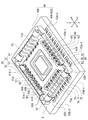
図1において、プラグコネクタIは、回路基板P1に取り付けられている。該プラグコネクタIは、電気絶縁材のプラグハウジング10に第一信号端子20と、第二信号端子30と、金具40が取り付けられていることで構成されている。
In FIG. 1, the plug connector I is attached to the circuit board P1. The plug connector I is configured by attaching a
プラグハウジング10は、回路基板P1の実装面に対面する平面形状が四角板形の底壁11と、底壁11の周囲から立ち上がる四角枠状の周壁12を有する。この周壁12は、四つの側壁から形成されており、第一方向としての第一端子配列方向Xに沿って延びる一対の側壁13と、この第一方向に直角な第二方向としての第二端子配列方向Yに沿って延びる他の一対の側壁14とを有している。すなわち、一対の側壁13は第二端子配列方向Yで対向して配置されており、他の一対の側壁14は第一端子配列方向Xで対向して配置されている。
The
図1において、空間に直交立体座標軸XYZを設定しており、プラグコネクタIのプラグハウジング10に設けられた周壁12の一対の側壁13が延び第一信号端子20を配列保持している方向を第一端子配列方向X、側壁13が延びる方向に直角な方向で他の一対の側壁14が延び第二信号端子30を配列保持している方向を第二端子配列方向Yとしている。したがって、第一端子配列方向Xと第二端子配列方向Yとを含む面に位置する底壁11に直角な方向をコネクタの挿抜方向Zとしている。
In FIG. 1, an orthogonal solid coordinate axis XYZ is set in space, and a direction in which a pair of
プラグハウジング10の一対の側壁13と他の一対の側壁14とは、それらの端部をなす四箇所で隅部15によって連結されていて、挿抜方向Zから見て四角枠状をなす周壁12を形成している。側壁13には第一端子配列方向Xで両方の端部、すなわち隅部15寄りの位置に金具40が配され、両金具40間に複数の第一信号端子20が配されている。金具40は、挿抜方向Zから見てL字状に屈曲されていて、後述するように、一部が隅部15を越えて側壁14の方にまで及んでいる。側壁14は、第二端子配列方向Yで、隅部15の近傍で金具40の一部を保持しているとともに、両方の隅部15の間で複数の第二信号端子30を配列保持している。
The pair of
周壁12の内側には、該周壁12と間隔をもった位置で該周壁12に囲まれるようにして、四角枠状の内側嵌合壁16が底壁11から起立して設けられている。内側嵌合壁16は、四つの壁がそれぞれ側壁13および側壁14と平行に延びている。
Inside the
図1に示されるように回路基板P1に取り付けられたプラグコネクタIは、図2に示されるように他の回路基板P2に取り付けられた相手コネクタとしてのレセプタクルコネクタIIに嵌合されるが、例えば図3に見られるようにレセプタクルコネクタIIが下方に位置して配置されて、プラグコネクタIは、図1の姿勢を上下反転して上方から該レセプタクルコネクタIIに嵌合される。 The plug connector I attached to the circuit board P1 as shown in FIG. 1 is fitted to the receptacle connector II as a mating connector attached to another circuit board P2 as shown in FIG. 2, for example. As can be seen in FIG. 3, the receptacle connector II is arranged at a lower position, and the plug connector I is fitted to the receptacle connector II from above by turning the posture of FIG. 1 upside down.
次に、図1及び図3そして図4を参照して、プラグコネクタIの第一信号端子20、金具40および第二信号端子30について順に説明する。
Next, the
第一信号端子20は、プラグハウジング10の側壁13に第一端子配列方向Xに沿って所定の間隔をもって複数配列保持されている。本実施形態では、第一信号端子20は、プラグハウジング10との一体モールド成形で、側壁13により保持されている。第一信号端子20は、金属帯状素材を屈曲して作られており、側壁13の内面と上面(図3では下面)そして外面の一部に及んで側壁13により保持される被保持部21と、側壁13の底面に位置して外方に延び、回路基板P1のパッドP1A−1に半田接続される接続部22とを有している。被保持部21のうち側壁13の内面に位置する部分と外面に位置する部分とは、レセプタクルコネクタIIの相手端子と接触するための内側接触部21Aと外側接触部21Bとをそれぞれ形成する。外側接触部21Bの端部には段部が形成されており、ロック部21B−1をなしている。
A plurality of
金具40は、第一端子配列方向Xで第一信号端子20の配列範囲の外側に位置しており、第一信号端子20より幅広の金属帯状素材を屈曲して作られていて、コネクタの挿抜方向Zから見てL字状に屈曲していて、側壁13に位置する第一金具部40Aと側壁14に位置する第二金具部40Bとを有している。第一金具部40Aは、プラグハウジング10との一体モールド成形により、第一信号端子20と同様に側壁13の内面と上面(図3では下棉)そして外面の一部に及んで側壁13により保持される被保持部41と、側壁13の内面側から底面にまわり込み外方に延び、回路基板P1のパッドP1A−2に半田接続される接続部42とを有している。被保持部41のうち側壁13の内面に位置する部分と外面に位置する部分とは、レセプタクルコネクタIIの相手金具と接触するための内側接触部41Aと外側接触部41Bとをそれぞれ形成する。外側接触部41Bの端部には段部が形成されており、ロック部41B−1をなしている。一方、第二金具部40Bは、プラグハウジング10の隅部15内に埋設されている連結部(図示されず)を介して第一金具部40Aとつながっており、その一部が側壁14の上面から外面にかけて露呈するように位置している。側壁14に位置し回路基板P1のパッドP1B−2に半田接続される第二金具部40Bの接続部は、側壁14内に埋設された部分から底面に突出し該底面に面する範囲に位置しており、図1そして図3には表われていない。かかる金具40は、補強金具として供するのみならず、電源端子としても使用可能である。
The
第二信号端子30は、基本的には、第一信号端子20に類似した形態をなしており、側壁14に第二端子配列方向Yに沿って所定の間隔をもって複数配列保持されている。第二信号端子30は、第二端子配列方向Yで両方の端部に位置する第二金具部40Bの間に配列されている。本実施形態では、第二信号端子30は、プラグハウジング10との一体モールド成形で、側壁14により保持されている。第二信号端子30は、金属帯状素材を屈曲して作られており、側壁14の内面と上面(図3では下面)そして外面の一部に及んで側壁14により保持される被保持部31と、側壁14の底面に位置して外方に延び、回路基板P1のパッドP1B−1に半田接続される接続部32とを有している。第二信号端子30を保持する側壁14は、第一信号端子20を保持する側壁13よりも壁厚(第一端子配列方向Xでの壁の厚み)が大きく設定されている。したがって、被保持部31の側壁14の上面に位置する部分は、第一信号端子20の対応部分より大きくなっている。被保持部31のうち側壁14の内面に位置する部分と外面に位置する部分とは、レセプタクルコネクタIIの相手端子と接触するための内側接触部31Aと外側接触部31Bとをそれぞれ形成する。外側接触部31Bの端部には四角形に没入して形成されたロック部31B−1が設けられている。
The
プラグコネクタIに嵌合される相手コネクタとしてのレセプタクルコネクタIIは、図2に見られるごとく、プラグコネクタIとは別の回路基板P2に取り付けられている。このレセプタクルコネクタIIにおいても、プラグコネクタIと同じ直交立体座標軸XYZ、すなわち、第一端子配列方向X、第二端子配列方向Yそしてコネクタ高さ方向Zが設定されている。 As seen in FIG. 2, the receptacle connector II as a mating connector fitted to the plug connector I is attached to a circuit board P2 different from the plug connector I. Also in this receptacle connector II, the same orthogonal solid coordinate axes XYZ as the plug connector I, that is, the first terminal arrangement direction X, the second terminal arrangement direction Y, and the connector height direction Z are set.
レセプタクルコネクタIIは、プラグコネクタIの場合と同様に、電気絶縁材のレセプタクルハウジング50に第一信号端子60と、第二信号端子70と、電源端子80と、金具90が取り付けられていることで構成されている。
Similar to the case of the plug connector I, the receptacle connector II has a
レセプタクルハウジング50は、回路基板P2の実装面に対面する平面形状が四角形板状をなし底壁を兼ねている中央壁51と、中央壁51の周囲に設けられた四角枠状の周壁52を有する。周壁52は、四つの側壁から形成されており、第一方向としての第一端子配列方向Xに沿って延びる一対の側壁53と、この第一方向に直角な第二方向としての第二端子配列方向Yに沿って延びる他の一対の側壁54とを有している。すなわち、一対の側壁53は、第二端子配列方向Yで対向して配置されており、他の一対の側壁54は第一端子配列方向Xで対向して配置されている。側壁53と側壁54は、隅部55により連結されている。隅部55は、コネクタの挿抜方向Zで側壁53および側壁54より高く形成されていて、隅部55の内側上面にはテーパ部55Aが形成されている。中央壁51と周壁52との間には、プラグコネクタIの周壁12が嵌合する四角環状の嵌合溝56が形成されている。中央壁51の外周縁、すなわち中央壁51における嵌合溝56側の周縁には、後述の第一信号端子60、電源端子80および第二信号端子70のそれぞれの端子の自由端側を収容し、該自由端側の弾性変位を許容する端子自由端側収容凹部56A,56B,56Cが形成されている。
The
中央壁51には、コネクタの挿抜方向Zで没入して形成された四角環状の内側嵌合環状溝57が設けられており、該内側環状溝57に、プラグコネクタIの内側嵌合壁16が嵌合するようになっている。
The
次に、図2ないし図4を参照して、レセプタクルコネクタIIの第一信号端子60、電源端子80、金具90および第二信号端子70について順に説明する。
Next, with reference to FIGS. 2 to 4, the
第一信号端子60は、レセプタクルハウジング50の側壁53に第一端子配列方向Xに沿って所定の間隔をもって複数配列保持されている。本実施形態では、第一信号端子60は、レセプタクルハウジング50との一体モールド成形で、側壁53により保持されている。第一信号端子60は、金属帯状素材を屈曲して作られており、側壁53の内面と上面に及んで側壁53の壁厚内に埋設保持される部分を有し、逆U字状をなす被保持部61と、側壁53の底面に位置して外方に延び、回路基板P2のパッドP2A−1に半田接続される接続部62と、嵌合溝56内に位置するU字状の弾性腕部63とを有している。被保持部61のうち側壁53の内面に位置する部分は、プラグコネクタIの相手端子と接触するための外側接触部61Aを形成している。この外側接触部61Aの下方には没入部が形成されており、ロック部61A−1をなしている。また、弾性腕部63の自由端側は、レセプタクルハウジング50の底部位置から端子自由端側収容凹部56A内で挿抜方向Zに沿って立ち上がり、その先端(図2,3にて上端)側に側壁53側に向け凸弯曲した内側接触部63Aを形成している。かくして、第二信号端子60は、外側接触部61Aと内側接触部63Aとで、プラグコネクタIの第一信号端子20を挟圧するようにして第一信号端子20と接触する。
A plurality of
電源端子80は、側壁53に複数配列されている第一信号端子60の配列範囲の外側に位置し、隅部55に隣接するように設けられている。本実施形態では、電源端子80は、レセプタクルハウジング50との一体モールド成形で、側壁53により保持されている。電源端子80は、金属帯状素材を屈曲して作られていて第一信号端子60より幅(第一端子配列方向Xでの寸法)が大きくなっており、側壁53の内面と上面に及んで側壁53の壁厚内に埋設保持される部分を有し、逆U字状をなす被保持部81と、側壁53の底面側に位置し外方に延び、回路基板P2のパッドP2A−2に半田接続される接続部82と、嵌合溝56内に位置するU字状の弾性腕部83とを有している。被保持部81のうち側壁53の内面に位置する部分は、プラグコネクタIの相手電源端子(プラグコネクタIの金具40が電源端子として用いられた場合の第一金具部40A)と接触するための外側接触部81Aを形成している。この外側接触部81Aの下方には没入部が形成されており、ロック部81A−1をなしている。また、弾性腕部83の自由端側は、レセプタクルハウジング50の底部位置から端子自由端側収容凹部56B内で立ち上がり、その先端(図2にて上端)側に側壁53側に向け凸弯曲した内側接触部83Aを形成している。かくして、電源端子80は、外側接触部81Aと内側接触部83Aとで、プラグコネクタIの金具40の第一金具部40Aを挟圧するようにして金具40と接触する。
The
金具90は、第一端子配列方向Xで第一信号端子60そして電源端子80の配列範囲の外側に位置しており、後述の第二信号端子70より幅広の金属帯状素材を屈曲して作られていて、コネクタの挿抜方向Zから見てL字状に屈曲していて、記側壁53に位置する第一金具部90Aと側壁54に位置する第二金具部90Bとを有している。第一金具部90Aは、レセプタクルハウジング50との一体モールド成形により、側壁53に埋設されている被保持部(したがって図には表われていない)と、側壁53の内面側から底面にまわり込み外方に延び、回路基板P2のパッドP2A−3に半田接続される接続部92Aとを有している。一方、第二金具部90Bは、隅部55内に埋設されている連結部(図示されず)を介して第一金具部90Aとつながっており、側壁54の上面から外面にかけて露呈するように位置している。側壁54に位置し回路基板P2のパッドP2B−2に半田接続される第二金具部90Bの接続部92Bは、側壁54の底面に面し外方に延出している。かかる金具90は、補強金具として供するのみならず、電源端子としても使用可能である。
The
第二信号端子70は、基本的には、第一信号端子60に類似した形態をなしており、側壁54に第二端子配列方向Yで所定の間隔をもって複数配列保持されている。第二信号端子70は、第二端子配列方向Yで両方の端部に位置する第二金具部90Bの間に配列されている。本実施形態では、第二信号端子70は、レセプタクルハウジング50との一体モールド成形で、側壁54により保持されている。側壁54は、第一信号端子60を配列している側壁53よりも壁厚(第一端子配列方向Xでの壁の厚み)が大きく設定されている。したがって、側壁54は、側壁53よりも強度が高い。第二信号端子70は、金属帯状素材を屈曲して作られており、側壁54の内面と上面に及んで側壁54の壁厚内に埋設保持される部分を有し、逆U字状をなす被保持部71と、側壁54の底面に位置し外方に延び、回路基板P2のパッドP2B−1に半田接続される接続部72と、嵌合溝56内に位置するU字状の弾性腕部73とを有している。被保持部71のうち側壁54の内面側に位置する部分は、プラグコネクタIの相手端子と接触するための外側接触部71Aを形成している。また、弾性腕部73の自由端側は、レセプタクルハウジング50の底部位置から端子自由端側収容凹部56C内で挿抜方向Zに沿って立ち上がり、その先端(図2,4にて上端)側に側壁54側に向け凸弯曲した内側接触部73Aを形成している。かくして、第二信号端子70は、外側接触部71Aと内側接触部73Aとで、プラグコネクタIの第二信号端子30を挟圧するようにして第二信号端子30と接触する。
The
このような本実施形態のプラグコネクタIとレセプタクルコネクタIIは、次の要領でコネクタ組立体として使用される。 Such a plug connector I and a receptacle connector II of the present embodiment are used as a connector assembly in the following manner.
プラグコネクタIは回路基板P1、レセプタクルコネクタIIは回路基板P2に取り付けられる。プラグコネクタIは、第一信号端子20の接続部22がパッドP1A−1に、金具40における第一金具部40Aの接続部42がパッドP1A−2に、第二金具部40Bの接続部(図示されず)がパッドP1B−2に、第二信号端子30の接続部32がパッドP1B−1にそれぞれ半田接続されることで回路基板P1に取り付けられる。一方、レセプタクルコネクタIIは、第一信号端子60の接続部62がパッドP2A−1に、電源端子80の接続部82がパッドP2A−2に、金具90における第一金具部90Aの接続部92がパッドP2A−3に、第二金具部90Bの接続部92BがパッドP2B−2にそれぞれ半田接続されることで回路基板P2に取り付けられる。
The plug connector I is attached to the circuit board P1, and the receptacle connector II is attached to the circuit board P2. In the plug connector I, the
このようにして、回路基板P1に取り付けられたプラグコネクタIと回路基板P2に取り付けられたレセプタクルコネクタIIは、回路基板P1,P2の図示を省略した図3および図4に見られるように、互いに上下方向をコネクタの挿抜方向Zとした姿勢で対向して配置された後、プラグコネクタIの周壁12がレセプタクルコネクタの嵌合溝56へ、プラグコネクタIの内側嵌合壁16がレセプタクルコネクタIIの内側環状溝57へそれぞれ挿入されることで接続される。
In this way, the plug connector I attached to the circuit board P1 and the receptacle connector II attached to the circuit board P2 are attached to each other as seen in FIGS. 3 and 4 in which the circuit boards P1 and P2 are not shown. After being arranged facing each other with the vertical direction as the connector insertion / removal direction Z, the
かくして、プラグコネクタIの第一信号端子20と第二信号端子30は、レセプタクルコネクタIIの第一信号端子60と第二信号端子70にそれぞれ接続され、さらに、プラグコネクタIの金具40の第一金具部40Aと第二金具部40Bは、レセプタクルコネクタIIの電源端子80と金具90にそれぞれ接続される。
Thus, the
プラグコネクタIのレセプタクルコネクタIIからの抜出時には、プラグコネクタIは挿抜方向Z方向で上方にもち上げられる。 When the plug connector I is pulled out from the receptacle connector II, the plug connector I is lifted upward in the insertion / removal direction Z direction.
プラグコネクタIがレセプタクルコネクタIIに対して挿抜されるとき、特に抜出されるときには、プラグコネクタIをレセプタクルコネクタIIの回路基板P2の実装面に対して一方そして他方へ傾けることを繰り返す、いわゆるこじり操作が行われることが多い。このようなこじり操作は、各端子やハウジングが変形または破損する原因となるおそれがあり、好ましくない。本実施形態では、このこじりにおける傾きの方向は、第一端子配列方向Xで対向する一対の側壁14の一方と他方に繰り返す方向にて行われるように規定されている。第一端子配列方向Xで対向するプラグコネクタIの側壁14は側壁13より壁厚が大きく構成され、同様に、第一端子配列方向Xで対向するレセプタクルコネクタIIの側壁54は側壁53より壁厚が大きく構成されている。このような構成により、側壁14および側壁54は、こじりによる曲げ応力に十分耐えられる。一方、こじり操作の方向ではない第二端子配列Y方向で対向する側壁13および側壁53は、こじりによる曲げ応力を受けることがないので、壁厚を小さく設定することができ、プラグコネクタIそしてレセプタクルコネクタIIともに、第二端子配列方向Yでの寸法をその分だけ小さくすることができる。
When the plug connector I is inserted into and removed from the receptacle connector II, especially when it is pulled out, the plug connector I is repeatedly tilted to one side and the other side with respect to the mounting surface of the circuit board P2 of the receptacle connector II, a so-called prying operation. Is often done. Such a prying operation may cause deformation or damage of each terminal or housing, which is not preferable. In the present embodiment, the direction of inclination in this prying is defined to be repeated in one and the other of the pair of
本実施形態では、レセプタクルコネクタIIのレセプタクルハウジング50における隅部15の高さが、第一信号端子60が配列されている部分の側壁53および第二信号端子70が配列されている部分の側壁54の高さよりもコネクタの挿抜方向Zで高く形成されている。そのため、プラグコネクタIが正規位置から多少ずれてレセプタクルコネクタIIに挿入されようとしても、プラグコネクタIは第一信号端子60と第二信号端子70に衝突せずに隅部15に衝突して正規位置へ誘導されるので、これらの信号端子は保護される。特に、この隅部15に金具が配置されていると、その保護の機能はさらに高められる。
In the present embodiment, the height of the
本実施形態では、プラグコネクタIとレセプタクルコネクタIIの両方とも、側壁の壁厚を第二端子配列方向Yに延びる側壁の方が第一端子配列方向Xに延びる側壁よりも大きくするように寸法関係を設定したが、両コネクタのうち一方だけに、第一端子配列方向Xでのこじりに対する強度の向上そして第二端子配列方向Yでの小型化を図るだけでよい場合には、この一方のコネクタに、かかる寸法関係を設定すれば十分である。 In the present embodiment, both the plug connector I and the receptacle connector II are dimensionally related so that the wall thickness of the side wall is larger in the side wall extending in the second terminal arrangement direction Y than in the side wall extending in the first terminal arrangement direction X. However, if it is only necessary to improve the strength against prying in the first terminal arrangement direction X and reduce the size in the second terminal arrangement direction Y for only one of the two connectors, this one connector It is sufficient to set such a dimensional relationship.
本発明において、一方の一対の側壁を他方の一対の側壁よりも端子配列方向での長さを大きくして、他方の一対の側壁の方向への傾きをもつようにこじりを許容すれば、他方の一対の側壁は前記一方の一対の側壁よりも短いのでそれだけこじりによる曲げ応力に強くなる。 In the present invention, if one pair of side walls is made longer in the terminal arrangement direction than the other pair of side walls and is allowed to be twisted so as to have an inclination in the direction of the other pair of side walls, the other. Since the pair of side walls is shorter than the pair of side walls, it is more resistant to bending stress due to prying.
10 (プラグ)ハウジング 52 周壁
11 底壁 53 側壁
12 周壁 54 側壁
13 側壁 55 隅部
14 側壁 60 (第一)信号端子
15 隅部 70 (第二)信号端子
20 (第一)信号端子 90 金具
30 (第二)信号端子 P1 回路基板
40 金具 P2 回路基板
50 (レセプタクル)ハウジング I (プラグ)コネクタ
51 中央壁 II (レセプタクル)コネクタ
10 (Plug)
Claims (5)
前記四つの側壁は、前記実装面に平行な第一方向に沿って延びる一対の側壁と、前記第一方向に対して直角な第二方向に沿って延びる他の一対の側壁とを有しており、
前記他の一対の側壁の壁厚は、前記一対の側壁の壁厚よりも大きく構成されており、
前記信号端子は、前記四つの側壁のそれぞれで複数保持されており、
前記一対の側壁に保持される前記信号端子の形状と前記他の一対の側壁に保持される前記信号端子の形状とが異なっていることを特徴とする回路基板用電気コネクタ。 An electric connector for a circuit board that is arranged on a mounting surface of a circuit board and whose direction perpendicular to the mounting surface is the insertion / extraction direction with the electric connector for the circuit board on the other side, and is held by the housing and the housing. The housing includes a plurality of signal terminals, and the housing has a bottom wall facing the mounting surface and a square frame-shaped peripheral wall that rises from the bottom wall in the insertion / removal direction and is formed by four side walls. In an electric connector for a circuit board in which the plurality of signal terminals are held on four side walls,
The four side walls have a pair of side walls extending along a first direction parallel to the mounting surface and another pair of side walls extending along a second direction perpendicular to the first direction. Ori,
The wall thickness of the other pair of side walls is configured to be larger than the wall thickness of the pair of side walls .
A plurality of the signal terminals are held on each of the four side walls.
An electric connector for a circuit board, characterized in that the shape of the signal terminal held on the pair of side walls and the shape of the signal terminal held on the other pair of side walls are different.
前記隅部の前記挿抜方向の高さは、前記各側壁における前記複数の信号端子の配列範囲の高さよりも高く形成されていることとする請求項1に記載の回路基板用電気コネクタ。 The housing has a corner connecting the pair of side walls and the other pair of side walls.
The electric connector for a circuit board according to claim 1, wherein the height of the corner portion in the insertion / removal direction is formed higher than the height of the arrangement range of the plurality of signal terminals on each side wall.
いずれの回路基板用コネクタも、前記実装面に平行な第一方向に沿って延びる一対の側壁と、前記第一方向に対して直角な第二方向に沿って延びる他の一対の側壁とを有しており、
前記他の一対の側壁の壁厚は、前記一対の側壁の壁厚よりも大きく構成されており、
前記信号端子は、前記四つの側壁のそれぞれで複数保持されており、
前記一対の側壁に保持される前記信号端子の形状と前記他の一対の側壁に保持される前記信号端子の形状とが異なっていることを特徴とする回路基板用電気コネクタの組立体。 It has two circuit board electric connectors arranged on each mounting surface of two parallel circuit boards and fitted to each other with the direction perpendicular to the mounting surface as the insertion / extraction direction, and any circuit board electric connector. Also has a bottom wall facing the mounting surface and a square frame-shaped peripheral wall rising from the bottom wall in the insertion / removal direction and formed by four side walls, and a plurality of signal terminals are held on the four side walls. In the assembly of electrical connectors for circuit boards
Connector for any of the circuit board is also closed and a pair of side walls extending along a first direction parallel to the mounting surface, and another pair of side walls extending along a second direction perpendicular to said first direction And
The wall thickness of the other pair of side walls is configured to be larger than the wall thickness of the pair of side walls .
A plurality of the signal terminals are held on each of the four side walls.
An assembly of an electric connector for a circuit board, characterized in that the shape of the signal terminal held on the pair of side walls and the shape of the signal terminal held on the other pair of side walls are different.
Priority Applications (1)
| Application Number | Priority Date | Filing Date | Title |
|---|---|---|---|
| JP2018021696A JP6978956B2 (en) | 2018-02-09 | 2018-02-09 | Electrical connector for circuit board and its assembly |
Applications Claiming Priority (1)
| Application Number | Priority Date | Filing Date | Title |
|---|---|---|---|
| JP2018021696A JP6978956B2 (en) | 2018-02-09 | 2018-02-09 | Electrical connector for circuit board and its assembly |
Publications (2)
| Publication Number | Publication Date |
|---|---|
| JP2019139938A JP2019139938A (en) | 2019-08-22 |
| JP6978956B2 true JP6978956B2 (en) | 2021-12-08 |
Family
ID=67694227
Family Applications (1)
| Application Number | Title | Priority Date | Filing Date |
|---|---|---|---|
| JP2018021696A Active JP6978956B2 (en) | 2018-02-09 | 2018-02-09 | Electrical connector for circuit board and its assembly |
Country Status (1)
| Country | Link |
|---|---|
| JP (1) | JP6978956B2 (en) |
Families Citing this family (2)
| Publication number | Priority date | Publication date | Assignee | Title |
|---|---|---|---|---|
| TWM622358U (en) * | 2021-04-22 | 2022-01-21 | 禾昌興業股份有限公司 | Polygon connector |
| CN115377759A (en) * | 2021-05-17 | 2022-11-22 | 日本航空电子工业株式会社 | Connector and connector assembly |
Family Cites Families (3)
| Publication number | Priority date | Publication date | Assignee | Title |
|---|---|---|---|---|
| JP2013101909A (en) * | 2011-10-14 | 2013-05-23 | Molex Inc | Connector |
| JP2016110706A (en) * | 2014-12-02 | 2016-06-20 | タイコエレクトロニクスジャパン合同会社 | Connector assembly |
| JP6319210B2 (en) * | 2015-07-02 | 2018-05-09 | Smk株式会社 | Connector and connector device |
-
2018
- 2018-02-09 JP JP2018021696A patent/JP6978956B2/en active Active
Also Published As
| Publication number | Publication date |
|---|---|
| JP2019139938A (en) | 2019-08-22 |
Similar Documents
| Publication | Publication Date | Title |
|---|---|---|
| JP6591251B2 (en) | connector | |
| KR102041368B1 (en) | Receptacle connector and connector assembly including the same | |
| US9397423B2 (en) | Board-to-board connector | |
| JP6150423B2 (en) | connector | |
| JP5232202B2 (en) | Circuit board electrical connector | |
| JP4030954B2 (en) | Receptacle electrical connector | |
| TWI667849B (en) | Connector | |
| JP2017162774A (en) | Electrical connector for circuit board | |
| JP6978956B2 (en) | Electrical connector for circuit board and its assembly | |
| JP5444285B2 (en) | Circuit board electrical connector | |
| JP5203029B2 (en) | Electrical connector | |
| JP5444284B2 (en) | Electrical connector | |
| JP5444283B2 (en) | Electrical connector and electrical connector assembly | |
| JP7385771B2 (en) | Socket reinforcement member, board-to-board socket and board-to-board connector assembly | |
| TW201509007A (en) | Connector | |
| US7950946B2 (en) | Electrical connector for receiving CPU | |
| CN112018535A (en) | Electric connector assembly | |
| JP7379309B2 (en) | A protective member for protecting a connector equipped with a housing having a central convex portion, and a connector in which the protective member is arranged | |
| JP2017147171A (en) | connector | |
| JP5659212B2 (en) | Circuit board electrical connector | |
| JP2022088211A (en) | Electric connector for circuit board and electric connector assembly | |
| JP2020187953A (en) | Board connector and board connector structure | |
| CN219371469U (en) | Board-to-board plug | |
| JP2018073536A (en) | Electric connector for board connection | |
| TWI837329B (en) | Electrical connector assembly |
Legal Events
| Date | Code | Title | Description |
|---|---|---|---|
| A621 | Written request for application examination |
Free format text: JAPANESE INTERMEDIATE CODE: A621 Effective date: 20201014 |
|
| A977 | Report on retrieval |
Free format text: JAPANESE INTERMEDIATE CODE: A971007 Effective date: 20210727 |
|
| A131 | Notification of reasons for refusal |
Free format text: JAPANESE INTERMEDIATE CODE: A131 Effective date: 20210817 |
|
| A521 | Written amendment |
Free format text: JAPANESE INTERMEDIATE CODE: A523 Effective date: 20210907 |
|
| TRDD | Decision of grant or rejection written | ||
| A01 | Written decision to grant a patent or to grant a registration (utility model) |
Free format text: JAPANESE INTERMEDIATE CODE: A01 Effective date: 20211026 |
|
| A61 | First payment of annual fees (during grant procedure) |
Free format text: JAPANESE INTERMEDIATE CODE: A61 Effective date: 20211112 |
|
| R150 | Certificate of patent or registration of utility model |
Ref document number: 6978956 Country of ref document: JP Free format text: JAPANESE INTERMEDIATE CODE: R150 |