JP6974446B2 - Fin field effect transistor (FET) that applies stress to the channel region using a dielectric material layer - Google Patents
Fin field effect transistor (FET) that applies stress to the channel region using a dielectric material layer Download PDFInfo
- Publication number
- JP6974446B2 JP6974446B2 JP2019513978A JP2019513978A JP6974446B2 JP 6974446 B2 JP6974446 B2 JP 6974446B2 JP 2019513978 A JP2019513978 A JP 2019513978A JP 2019513978 A JP2019513978 A JP 2019513978A JP 6974446 B2 JP6974446 B2 JP 6974446B2
- Authority
- JP
- Japan
- Prior art keywords
- dielectric material
- material layer
- fin
- finfet
- channel region
- Prior art date
- Legal status (The legal status is an assumption and is not a legal conclusion. Google has not performed a legal analysis and makes no representation as to the accuracy of the status listed.)
- Active
Links
- 239000003989 dielectric material Substances 0.000 title claims description 134
- 230000005669 field effect Effects 0.000 title claims description 8
- 239000000758 substrate Substances 0.000 claims description 63
- 238000000034 method Methods 0.000 claims description 37
- 239000000463 material Substances 0.000 claims description 18
- 238000000137 annealing Methods 0.000 claims description 6
- 238000005229 chemical vapour deposition Methods 0.000 claims description 6
- 238000005530 etching Methods 0.000 claims description 4
- 238000004519 manufacturing process Methods 0.000 description 22
- 230000008569 process Effects 0.000 description 19
- 230000006870 function Effects 0.000 description 9
- 238000003860 storage Methods 0.000 description 6
- 238000012545 processing Methods 0.000 description 4
- 238000007796 conventional method Methods 0.000 description 3
- 238000013461 design Methods 0.000 description 3
- VYPSYNLAJGMNEJ-UHFFFAOYSA-N Silicium dioxide Chemical compound O=[Si]=O VYPSYNLAJGMNEJ-UHFFFAOYSA-N 0.000 description 2
- 238000004891 communication Methods 0.000 description 2
- 239000013078 crystal Substances 0.000 description 2
- 230000000694 effects Effects 0.000 description 2
- 238000005516 engineering process Methods 0.000 description 2
- 239000002184 metal Substances 0.000 description 2
- 238000004904 shortening Methods 0.000 description 2
- 229910052581 Si3N4 Inorganic materials 0.000 description 1
- 238000003491 array Methods 0.000 description 1
- 230000001413 cellular effect Effects 0.000 description 1
- 230000008859 change Effects 0.000 description 1
- 230000007423 decrease Effects 0.000 description 1
- 238000010586 diagram Methods 0.000 description 1
- 239000004744 fabric Substances 0.000 description 1
- 230000036541 health Effects 0.000 description 1
- 230000000977 initiatory effect Effects 0.000 description 1
- 238000002955 isolation Methods 0.000 description 1
- 239000004973 liquid crystal related substance Substances 0.000 description 1
- 239000006249 magnetic particle Substances 0.000 description 1
- 230000000116 mitigating effect Effects 0.000 description 1
- 238000012986 modification Methods 0.000 description 1
- 230000004048 modification Effects 0.000 description 1
- 230000003287 optical effect Effects 0.000 description 1
- 230000003071 parasitic effect Effects 0.000 description 1
- 239000002245 particle Substances 0.000 description 1
- 238000000926 separation method Methods 0.000 description 1
- 235000012239 silicon dioxide Nutrition 0.000 description 1
- 239000000377 silicon dioxide Substances 0.000 description 1
- HQVNEWCFYHHQES-UHFFFAOYSA-N silicon nitride Chemical compound N12[Si]34N5[Si]62N3[Si]51N64 HQVNEWCFYHHQES-UHFFFAOYSA-N 0.000 description 1
- 230000000007 visual effect Effects 0.000 description 1
Images


Classifications
-
- H—ELECTRICITY
- H01—ELECTRIC ELEMENTS
- H01L—SEMICONDUCTOR DEVICES NOT COVERED BY CLASS H10
- H01L29/00—Semiconductor devices adapted for rectifying, amplifying, oscillating or switching, or capacitors or resistors with at least one potential-jump barrier or surface barrier, e.g. PN junction depletion layer or carrier concentration layer; Details of semiconductor bodies or of electrodes thereof ; Multistep manufacturing processes therefor
- H01L29/66—Types of semiconductor device ; Multistep manufacturing processes therefor
- H01L29/68—Types of semiconductor device ; Multistep manufacturing processes therefor controllable by only the electric current supplied, or only the electric potential applied, to an electrode which does not carry the current to be rectified, amplified or switched
- H01L29/76—Unipolar devices, e.g. field effect transistors
- H01L29/772—Field effect transistors
- H01L29/78—Field effect transistors with field effect produced by an insulated gate
- H01L29/7842—Field effect transistors with field effect produced by an insulated gate means for exerting mechanical stress on the crystal lattice of the channel region, e.g. using a flexible substrate
- H01L29/7846—Field effect transistors with field effect produced by an insulated gate means for exerting mechanical stress on the crystal lattice of the channel region, e.g. using a flexible substrate the means being located in the lateral device isolation region, e.g. STI
-
- H—ELECTRICITY
- H01—ELECTRIC ELEMENTS
- H01L—SEMICONDUCTOR DEVICES NOT COVERED BY CLASS H10
- H01L29/00—Semiconductor devices adapted for rectifying, amplifying, oscillating or switching, or capacitors or resistors with at least one potential-jump barrier or surface barrier, e.g. PN junction depletion layer or carrier concentration layer; Details of semiconductor bodies or of electrodes thereof ; Multistep manufacturing processes therefor
- H01L29/66—Types of semiconductor device ; Multistep manufacturing processes therefor
- H01L29/68—Types of semiconductor device ; Multistep manufacturing processes therefor controllable by only the electric current supplied, or only the electric potential applied, to an electrode which does not carry the current to be rectified, amplified or switched
- H01L29/76—Unipolar devices, e.g. field effect transistors
- H01L29/772—Field effect transistors
- H01L29/78—Field effect transistors with field effect produced by an insulated gate
- H01L29/785—Field effect transistors with field effect produced by an insulated gate having a channel with a horizontal current flow in a vertical sidewall of a semiconductor body, e.g. FinFET, MuGFET
-
- H—ELECTRICITY
- H01—ELECTRIC ELEMENTS
- H01L—SEMICONDUCTOR DEVICES NOT COVERED BY CLASS H10
- H01L21/00—Processes or apparatus adapted for the manufacture or treatment of semiconductor or solid state devices or of parts thereof
- H01L21/02—Manufacture or treatment of semiconductor devices or of parts thereof
- H01L21/02104—Forming layers
- H01L21/02107—Forming insulating materials on a substrate
- H01L21/02225—Forming insulating materials on a substrate characterised by the process for the formation of the insulating layer
- H01L21/0226—Forming insulating materials on a substrate characterised by the process for the formation of the insulating layer formation by a deposition process
- H01L21/02263—Forming insulating materials on a substrate characterised by the process for the formation of the insulating layer formation by a deposition process deposition from the gas or vapour phase
- H01L21/02271—Forming insulating materials on a substrate characterised by the process for the formation of the insulating layer formation by a deposition process deposition from the gas or vapour phase deposition by decomposition or reaction of gaseous or vapour phase compounds, i.e. chemical vapour deposition
-
- H—ELECTRICITY
- H01—ELECTRIC ELEMENTS
- H01L—SEMICONDUCTOR DEVICES NOT COVERED BY CLASS H10
- H01L21/00—Processes or apparatus adapted for the manufacture or treatment of semiconductor or solid state devices or of parts thereof
- H01L21/02—Manufacture or treatment of semiconductor devices or of parts thereof
- H01L21/04—Manufacture or treatment of semiconductor devices or of parts thereof the devices having at least one potential-jump barrier or surface barrier, e.g. PN junction, depletion layer or carrier concentration layer
- H01L21/18—Manufacture or treatment of semiconductor devices or of parts thereof the devices having at least one potential-jump barrier or surface barrier, e.g. PN junction, depletion layer or carrier concentration layer the devices having semiconductor bodies comprising elements of Group IV of the Periodic System or AIIIBV compounds with or without impurities, e.g. doping materials
- H01L21/30—Treatment of semiconductor bodies using processes or apparatus not provided for in groups H01L21/20 - H01L21/26
- H01L21/302—Treatment of semiconductor bodies using processes or apparatus not provided for in groups H01L21/20 - H01L21/26 to change their surface-physical characteristics or shape, e.g. etching, polishing, cutting
- H01L21/306—Chemical or electrical treatment, e.g. electrolytic etching
- H01L21/30604—Chemical etching
-
- H—ELECTRICITY
- H01—ELECTRIC ELEMENTS
- H01L—SEMICONDUCTOR DEVICES NOT COVERED BY CLASS H10
- H01L21/00—Processes or apparatus adapted for the manufacture or treatment of semiconductor or solid state devices or of parts thereof
- H01L21/70—Manufacture or treatment of devices consisting of a plurality of solid state components formed in or on a common substrate or of parts thereof; Manufacture of integrated circuit devices or of parts thereof
- H01L21/77—Manufacture or treatment of devices consisting of a plurality of solid state components or integrated circuits formed in, or on, a common substrate
- H01L21/78—Manufacture or treatment of devices consisting of a plurality of solid state components or integrated circuits formed in, or on, a common substrate with subsequent division of the substrate into plural individual devices
- H01L21/82—Manufacture or treatment of devices consisting of a plurality of solid state components or integrated circuits formed in, or on, a common substrate with subsequent division of the substrate into plural individual devices to produce devices, e.g. integrated circuits, each consisting of a plurality of components
- H01L21/822—Manufacture or treatment of devices consisting of a plurality of solid state components or integrated circuits formed in, or on, a common substrate with subsequent division of the substrate into plural individual devices to produce devices, e.g. integrated circuits, each consisting of a plurality of components the substrate being a semiconductor, using silicon technology
- H01L21/8232—Field-effect technology
- H01L21/8234—MIS technology, i.e. integration processes of field effect transistors of the conductor-insulator-semiconductor type
- H01L21/823418—MIS technology, i.e. integration processes of field effect transistors of the conductor-insulator-semiconductor type with a particular manufacturing method of the source or drain structures, e.g. specific source or drain implants or silicided source or drain structures or raised source or drain structures
-
- H—ELECTRICITY
- H01—ELECTRIC ELEMENTS
- H01L—SEMICONDUCTOR DEVICES NOT COVERED BY CLASS H10
- H01L21/00—Processes or apparatus adapted for the manufacture or treatment of semiconductor or solid state devices or of parts thereof
- H01L21/70—Manufacture or treatment of devices consisting of a plurality of solid state components formed in or on a common substrate or of parts thereof; Manufacture of integrated circuit devices or of parts thereof
- H01L21/77—Manufacture or treatment of devices consisting of a plurality of solid state components or integrated circuits formed in, or on, a common substrate
- H01L21/78—Manufacture or treatment of devices consisting of a plurality of solid state components or integrated circuits formed in, or on, a common substrate with subsequent division of the substrate into plural individual devices
- H01L21/82—Manufacture or treatment of devices consisting of a plurality of solid state components or integrated circuits formed in, or on, a common substrate with subsequent division of the substrate into plural individual devices to produce devices, e.g. integrated circuits, each consisting of a plurality of components
- H01L21/822—Manufacture or treatment of devices consisting of a plurality of solid state components or integrated circuits formed in, or on, a common substrate with subsequent division of the substrate into plural individual devices to produce devices, e.g. integrated circuits, each consisting of a plurality of components the substrate being a semiconductor, using silicon technology
- H01L21/8232—Field-effect technology
- H01L21/8234—MIS technology, i.e. integration processes of field effect transistors of the conductor-insulator-semiconductor type
- H01L21/823431—MIS technology, i.e. integration processes of field effect transistors of the conductor-insulator-semiconductor type with a particular manufacturing method of transistors with a horizontal current flow in a vertical sidewall of a semiconductor body, e.g. FinFET, MuGFET
-
- H—ELECTRICITY
- H01—ELECTRIC ELEMENTS
- H01L—SEMICONDUCTOR DEVICES NOT COVERED BY CLASS H10
- H01L21/00—Processes or apparatus adapted for the manufacture or treatment of semiconductor or solid state devices or of parts thereof
- H01L21/70—Manufacture or treatment of devices consisting of a plurality of solid state components formed in or on a common substrate or of parts thereof; Manufacture of integrated circuit devices or of parts thereof
- H01L21/77—Manufacture or treatment of devices consisting of a plurality of solid state components or integrated circuits formed in, or on, a common substrate
- H01L21/78—Manufacture or treatment of devices consisting of a plurality of solid state components or integrated circuits formed in, or on, a common substrate with subsequent division of the substrate into plural individual devices
- H01L21/82—Manufacture or treatment of devices consisting of a plurality of solid state components or integrated circuits formed in, or on, a common substrate with subsequent division of the substrate into plural individual devices to produce devices, e.g. integrated circuits, each consisting of a plurality of components
- H01L21/822—Manufacture or treatment of devices consisting of a plurality of solid state components or integrated circuits formed in, or on, a common substrate with subsequent division of the substrate into plural individual devices to produce devices, e.g. integrated circuits, each consisting of a plurality of components the substrate being a semiconductor, using silicon technology
- H01L21/8232—Field-effect technology
- H01L21/8234—MIS technology, i.e. integration processes of field effect transistors of the conductor-insulator-semiconductor type
- H01L21/823437—MIS technology, i.e. integration processes of field effect transistors of the conductor-insulator-semiconductor type with a particular manufacturing method of the gate conductors, e.g. particular materials, shapes
-
- H—ELECTRICITY
- H01—ELECTRIC ELEMENTS
- H01L—SEMICONDUCTOR DEVICES NOT COVERED BY CLASS H10
- H01L21/00—Processes or apparatus adapted for the manufacture or treatment of semiconductor or solid state devices or of parts thereof
- H01L21/70—Manufacture or treatment of devices consisting of a plurality of solid state components formed in or on a common substrate or of parts thereof; Manufacture of integrated circuit devices or of parts thereof
- H01L21/77—Manufacture or treatment of devices consisting of a plurality of solid state components or integrated circuits formed in, or on, a common substrate
- H01L21/78—Manufacture or treatment of devices consisting of a plurality of solid state components or integrated circuits formed in, or on, a common substrate with subsequent division of the substrate into plural individual devices
- H01L21/82—Manufacture or treatment of devices consisting of a plurality of solid state components or integrated circuits formed in, or on, a common substrate with subsequent division of the substrate into plural individual devices to produce devices, e.g. integrated circuits, each consisting of a plurality of components
- H01L21/822—Manufacture or treatment of devices consisting of a plurality of solid state components or integrated circuits formed in, or on, a common substrate with subsequent division of the substrate into plural individual devices to produce devices, e.g. integrated circuits, each consisting of a plurality of components the substrate being a semiconductor, using silicon technology
- H01L21/8232—Field-effect technology
- H01L21/8234—MIS technology, i.e. integration processes of field effect transistors of the conductor-insulator-semiconductor type
- H01L21/823481—MIS technology, i.e. integration processes of field effect transistors of the conductor-insulator-semiconductor type isolation region manufacturing related aspects, e.g. to avoid interaction of isolation region with adjacent structure
-
- H—ELECTRICITY
- H01—ELECTRIC ELEMENTS
- H01L—SEMICONDUCTOR DEVICES NOT COVERED BY CLASS H10
- H01L21/00—Processes or apparatus adapted for the manufacture or treatment of semiconductor or solid state devices or of parts thereof
- H01L21/70—Manufacture or treatment of devices consisting of a plurality of solid state components formed in or on a common substrate or of parts thereof; Manufacture of integrated circuit devices or of parts thereof
- H01L21/77—Manufacture or treatment of devices consisting of a plurality of solid state components or integrated circuits formed in, or on, a common substrate
- H01L21/78—Manufacture or treatment of devices consisting of a plurality of solid state components or integrated circuits formed in, or on, a common substrate with subsequent division of the substrate into plural individual devices
- H01L21/82—Manufacture or treatment of devices consisting of a plurality of solid state components or integrated circuits formed in, or on, a common substrate with subsequent division of the substrate into plural individual devices to produce devices, e.g. integrated circuits, each consisting of a plurality of components
- H01L21/822—Manufacture or treatment of devices consisting of a plurality of solid state components or integrated circuits formed in, or on, a common substrate with subsequent division of the substrate into plural individual devices to produce devices, e.g. integrated circuits, each consisting of a plurality of components the substrate being a semiconductor, using silicon technology
- H01L21/8232—Field-effect technology
- H01L21/8234—MIS technology, i.e. integration processes of field effect transistors of the conductor-insulator-semiconductor type
- H01L21/8238—Complementary field-effect transistors, e.g. CMOS
- H01L21/823821—Complementary field-effect transistors, e.g. CMOS with a particular manufacturing method of transistors with a horizontal current flow in a vertical sidewall of a semiconductor body, e.g. FinFET, MuGFET
-
- H—ELECTRICITY
- H01—ELECTRIC ELEMENTS
- H01L—SEMICONDUCTOR DEVICES NOT COVERED BY CLASS H10
- H01L21/00—Processes or apparatus adapted for the manufacture or treatment of semiconductor or solid state devices or of parts thereof
- H01L21/70—Manufacture or treatment of devices consisting of a plurality of solid state components formed in or on a common substrate or of parts thereof; Manufacture of integrated circuit devices or of parts thereof
- H01L21/77—Manufacture or treatment of devices consisting of a plurality of solid state components or integrated circuits formed in, or on, a common substrate
- H01L21/78—Manufacture or treatment of devices consisting of a plurality of solid state components or integrated circuits formed in, or on, a common substrate with subsequent division of the substrate into plural individual devices
- H01L21/82—Manufacture or treatment of devices consisting of a plurality of solid state components or integrated circuits formed in, or on, a common substrate with subsequent division of the substrate into plural individual devices to produce devices, e.g. integrated circuits, each consisting of a plurality of components
- H01L21/84—Manufacture or treatment of devices consisting of a plurality of solid state components or integrated circuits formed in, or on, a common substrate with subsequent division of the substrate into plural individual devices to produce devices, e.g. integrated circuits, each consisting of a plurality of components the substrate being other than a semiconductor body, e.g. being an insulating body
- H01L21/845—Manufacture or treatment of devices consisting of a plurality of solid state components or integrated circuits formed in, or on, a common substrate with subsequent division of the substrate into plural individual devices to produce devices, e.g. integrated circuits, each consisting of a plurality of components the substrate being other than a semiconductor body, e.g. being an insulating body including field-effect transistors with a horizontal current flow in a vertical sidewall of a semiconductor body, e.g. FinFET, MuGFET
-
- H—ELECTRICITY
- H01—ELECTRIC ELEMENTS
- H01L—SEMICONDUCTOR DEVICES NOT COVERED BY CLASS H10
- H01L27/00—Devices consisting of a plurality of semiconductor or other solid-state components formed in or on a common substrate
- H01L27/02—Devices consisting of a plurality of semiconductor or other solid-state components formed in or on a common substrate including semiconductor components specially adapted for rectifying, oscillating, amplifying or switching and having at least one potential-jump barrier or surface barrier; including integrated passive circuit elements with at least one potential-jump barrier or surface barrier
- H01L27/0203—Particular design considerations for integrated circuits
- H01L27/0207—Geometrical layout of the components, e.g. computer aided design; custom LSI, semi-custom LSI, standard cell technique
-
- H—ELECTRICITY
- H01—ELECTRIC ELEMENTS
- H01L—SEMICONDUCTOR DEVICES NOT COVERED BY CLASS H10
- H01L27/00—Devices consisting of a plurality of semiconductor or other solid-state components formed in or on a common substrate
- H01L27/02—Devices consisting of a plurality of semiconductor or other solid-state components formed in or on a common substrate including semiconductor components specially adapted for rectifying, oscillating, amplifying or switching and having at least one potential-jump barrier or surface barrier; including integrated passive circuit elements with at least one potential-jump barrier or surface barrier
- H01L27/04—Devices consisting of a plurality of semiconductor or other solid-state components formed in or on a common substrate including semiconductor components specially adapted for rectifying, oscillating, amplifying or switching and having at least one potential-jump barrier or surface barrier; including integrated passive circuit elements with at least one potential-jump barrier or surface barrier the substrate being a semiconductor body
- H01L27/08—Devices consisting of a plurality of semiconductor or other solid-state components formed in or on a common substrate including semiconductor components specially adapted for rectifying, oscillating, amplifying or switching and having at least one potential-jump barrier or surface barrier; including integrated passive circuit elements with at least one potential-jump barrier or surface barrier the substrate being a semiconductor body including only semiconductor components of a single kind
- H01L27/085—Devices consisting of a plurality of semiconductor or other solid-state components formed in or on a common substrate including semiconductor components specially adapted for rectifying, oscillating, amplifying or switching and having at least one potential-jump barrier or surface barrier; including integrated passive circuit elements with at least one potential-jump barrier or surface barrier the substrate being a semiconductor body including only semiconductor components of a single kind including field-effect components only
- H01L27/088—Devices consisting of a plurality of semiconductor or other solid-state components formed in or on a common substrate including semiconductor components specially adapted for rectifying, oscillating, amplifying or switching and having at least one potential-jump barrier or surface barrier; including integrated passive circuit elements with at least one potential-jump barrier or surface barrier the substrate being a semiconductor body including only semiconductor components of a single kind including field-effect components only the components being field-effect transistors with insulated gate
- H01L27/0886—Devices consisting of a plurality of semiconductor or other solid-state components formed in or on a common substrate including semiconductor components specially adapted for rectifying, oscillating, amplifying or switching and having at least one potential-jump barrier or surface barrier; including integrated passive circuit elements with at least one potential-jump barrier or surface barrier the substrate being a semiconductor body including only semiconductor components of a single kind including field-effect components only the components being field-effect transistors with insulated gate including transistors with a horizontal current flow in a vertical sidewall of a semiconductor body, e.g. FinFET, MuGFET
-
- H—ELECTRICITY
- H01—ELECTRIC ELEMENTS
- H01L—SEMICONDUCTOR DEVICES NOT COVERED BY CLASS H10
- H01L27/00—Devices consisting of a plurality of semiconductor or other solid-state components formed in or on a common substrate
- H01L27/02—Devices consisting of a plurality of semiconductor or other solid-state components formed in or on a common substrate including semiconductor components specially adapted for rectifying, oscillating, amplifying or switching and having at least one potential-jump barrier or surface barrier; including integrated passive circuit elements with at least one potential-jump barrier or surface barrier
- H01L27/04—Devices consisting of a plurality of semiconductor or other solid-state components formed in or on a common substrate including semiconductor components specially adapted for rectifying, oscillating, amplifying or switching and having at least one potential-jump barrier or surface barrier; including integrated passive circuit elements with at least one potential-jump barrier or surface barrier the substrate being a semiconductor body
- H01L27/08—Devices consisting of a plurality of semiconductor or other solid-state components formed in or on a common substrate including semiconductor components specially adapted for rectifying, oscillating, amplifying or switching and having at least one potential-jump barrier or surface barrier; including integrated passive circuit elements with at least one potential-jump barrier or surface barrier the substrate being a semiconductor body including only semiconductor components of a single kind
- H01L27/085—Devices consisting of a plurality of semiconductor or other solid-state components formed in or on a common substrate including semiconductor components specially adapted for rectifying, oscillating, amplifying or switching and having at least one potential-jump barrier or surface barrier; including integrated passive circuit elements with at least one potential-jump barrier or surface barrier the substrate being a semiconductor body including only semiconductor components of a single kind including field-effect components only
- H01L27/088—Devices consisting of a plurality of semiconductor or other solid-state components formed in or on a common substrate including semiconductor components specially adapted for rectifying, oscillating, amplifying or switching and having at least one potential-jump barrier or surface barrier; including integrated passive circuit elements with at least one potential-jump barrier or surface barrier the substrate being a semiconductor body including only semiconductor components of a single kind including field-effect components only the components being field-effect transistors with insulated gate
- H01L27/092—Devices consisting of a plurality of semiconductor or other solid-state components formed in or on a common substrate including semiconductor components specially adapted for rectifying, oscillating, amplifying or switching and having at least one potential-jump barrier or surface barrier; including integrated passive circuit elements with at least one potential-jump barrier or surface barrier the substrate being a semiconductor body including only semiconductor components of a single kind including field-effect components only the components being field-effect transistors with insulated gate complementary MIS field-effect transistors
- H01L27/0924—Devices consisting of a plurality of semiconductor or other solid-state components formed in or on a common substrate including semiconductor components specially adapted for rectifying, oscillating, amplifying or switching and having at least one potential-jump barrier or surface barrier; including integrated passive circuit elements with at least one potential-jump barrier or surface barrier the substrate being a semiconductor body including only semiconductor components of a single kind including field-effect components only the components being field-effect transistors with insulated gate complementary MIS field-effect transistors including transistors with a horizontal current flow in a vertical sidewall of a semiconductor body, e.g. FinFET, MuGFET
-
- H—ELECTRICITY
- H01—ELECTRIC ELEMENTS
- H01L—SEMICONDUCTOR DEVICES NOT COVERED BY CLASS H10
- H01L27/00—Devices consisting of a plurality of semiconductor or other solid-state components formed in or on a common substrate
- H01L27/02—Devices consisting of a plurality of semiconductor or other solid-state components formed in or on a common substrate including semiconductor components specially adapted for rectifying, oscillating, amplifying or switching and having at least one potential-jump barrier or surface barrier; including integrated passive circuit elements with at least one potential-jump barrier or surface barrier
- H01L27/12—Devices consisting of a plurality of semiconductor or other solid-state components formed in or on a common substrate including semiconductor components specially adapted for rectifying, oscillating, amplifying or switching and having at least one potential-jump barrier or surface barrier; including integrated passive circuit elements with at least one potential-jump barrier or surface barrier the substrate being other than a semiconductor body, e.g. an insulating body
- H01L27/1203—Devices consisting of a plurality of semiconductor or other solid-state components formed in or on a common substrate including semiconductor components specially adapted for rectifying, oscillating, amplifying or switching and having at least one potential-jump barrier or surface barrier; including integrated passive circuit elements with at least one potential-jump barrier or surface barrier the substrate being other than a semiconductor body, e.g. an insulating body the substrate comprising an insulating body on a semiconductor body, e.g. SOI
- H01L27/1211—Devices consisting of a plurality of semiconductor or other solid-state components formed in or on a common substrate including semiconductor components specially adapted for rectifying, oscillating, amplifying or switching and having at least one potential-jump barrier or surface barrier; including integrated passive circuit elements with at least one potential-jump barrier or surface barrier the substrate being other than a semiconductor body, e.g. an insulating body the substrate comprising an insulating body on a semiconductor body, e.g. SOI combined with field-effect transistors with a horizontal current flow in a vertical sidewall of a semiconductor body, e.g. FinFET, MuGFET
-
- H—ELECTRICITY
- H01—ELECTRIC ELEMENTS
- H01L—SEMICONDUCTOR DEVICES NOT COVERED BY CLASS H10
- H01L29/00—Semiconductor devices adapted for rectifying, amplifying, oscillating or switching, or capacitors or resistors with at least one potential-jump barrier or surface barrier, e.g. PN junction depletion layer or carrier concentration layer; Details of semiconductor bodies or of electrodes thereof ; Multistep manufacturing processes therefor
- H01L29/02—Semiconductor bodies ; Multistep manufacturing processes therefor
- H01L29/06—Semiconductor bodies ; Multistep manufacturing processes therefor characterised by their shape; characterised by the shapes, relative sizes, or dispositions of the semiconductor regions ; characterised by the concentration or distribution of impurities within semiconductor regions
- H01L29/08—Semiconductor bodies ; Multistep manufacturing processes therefor characterised by their shape; characterised by the shapes, relative sizes, or dispositions of the semiconductor regions ; characterised by the concentration or distribution of impurities within semiconductor regions with semiconductor regions connected to an electrode carrying current to be rectified, amplified or switched and such electrode being part of a semiconductor device which comprises three or more electrodes
- H01L29/0843—Source or drain regions of field-effect devices
- H01L29/0847—Source or drain regions of field-effect devices of field-effect transistors with insulated gate
-
- H—ELECTRICITY
- H01—ELECTRIC ELEMENTS
- H01L—SEMICONDUCTOR DEVICES NOT COVERED BY CLASS H10
- H01L29/00—Semiconductor devices adapted for rectifying, amplifying, oscillating or switching, or capacitors or resistors with at least one potential-jump barrier or surface barrier, e.g. PN junction depletion layer or carrier concentration layer; Details of semiconductor bodies or of electrodes thereof ; Multistep manufacturing processes therefor
- H01L29/40—Electrodes ; Multistep manufacturing processes therefor
- H01L29/41—Electrodes ; Multistep manufacturing processes therefor characterised by their shape, relative sizes or dispositions
- H01L29/417—Electrodes ; Multistep manufacturing processes therefor characterised by their shape, relative sizes or dispositions carrying the current to be rectified, amplified or switched
- H01L29/41725—Source or drain electrodes for field effect devices
- H01L29/41791—Source or drain electrodes for field effect devices for transistors with a horizontal current flow in a vertical sidewall, e.g. FinFET, MuGFET
-
- H—ELECTRICITY
- H01—ELECTRIC ELEMENTS
- H01L—SEMICONDUCTOR DEVICES NOT COVERED BY CLASS H10
- H01L29/00—Semiconductor devices adapted for rectifying, amplifying, oscillating or switching, or capacitors or resistors with at least one potential-jump barrier or surface barrier, e.g. PN junction depletion layer or carrier concentration layer; Details of semiconductor bodies or of electrodes thereof ; Multistep manufacturing processes therefor
- H01L29/66—Types of semiconductor device ; Multistep manufacturing processes therefor
- H01L29/66007—Multistep manufacturing processes
- H01L29/66075—Multistep manufacturing processes of devices having semiconductor bodies comprising group 14 or group 13/15 materials
- H01L29/66227—Multistep manufacturing processes of devices having semiconductor bodies comprising group 14 or group 13/15 materials the devices being controllable only by the electric current supplied or the electric potential applied, to an electrode which does not carry the current to be rectified, amplified or switched, e.g. three-terminal devices
- H01L29/66409—Unipolar field-effect transistors
- H01L29/66477—Unipolar field-effect transistors with an insulated gate, i.e. MISFET
- H01L29/66787—Unipolar field-effect transistors with an insulated gate, i.e. MISFET with a gate at the side of the channel
- H01L29/66795—Unipolar field-effect transistors with an insulated gate, i.e. MISFET with a gate at the side of the channel with a horizontal current flow in a vertical sidewall of a semiconductor body, e.g. FinFET, MuGFET
-
- H—ELECTRICITY
- H01—ELECTRIC ELEMENTS
- H01L—SEMICONDUCTOR DEVICES NOT COVERED BY CLASS H10
- H01L29/00—Semiconductor devices adapted for rectifying, amplifying, oscillating or switching, or capacitors or resistors with at least one potential-jump barrier or surface barrier, e.g. PN junction depletion layer or carrier concentration layer; Details of semiconductor bodies or of electrodes thereof ; Multistep manufacturing processes therefor
- H01L29/66—Types of semiconductor device ; Multistep manufacturing processes therefor
- H01L29/68—Types of semiconductor device ; Multistep manufacturing processes therefor controllable by only the electric current supplied, or only the electric potential applied, to an electrode which does not carry the current to be rectified, amplified or switched
- H01L29/76—Unipolar devices, e.g. field effect transistors
- H01L29/772—Field effect transistors
- H01L29/78—Field effect transistors with field effect produced by an insulated gate
- H01L29/7842—Field effect transistors with field effect produced by an insulated gate means for exerting mechanical stress on the crystal lattice of the channel region, e.g. using a flexible substrate
- H01L29/7843—Field effect transistors with field effect produced by an insulated gate means for exerting mechanical stress on the crystal lattice of the channel region, e.g. using a flexible substrate the means being an applied insulating layer
-
- H—ELECTRICITY
- H01—ELECTRIC ELEMENTS
- H01L—SEMICONDUCTOR DEVICES NOT COVERED BY CLASS H10
- H01L29/00—Semiconductor devices adapted for rectifying, amplifying, oscillating or switching, or capacitors or resistors with at least one potential-jump barrier or surface barrier, e.g. PN junction depletion layer or carrier concentration layer; Details of semiconductor bodies or of electrodes thereof ; Multistep manufacturing processes therefor
- H01L29/66—Types of semiconductor device ; Multistep manufacturing processes therefor
- H01L29/68—Types of semiconductor device ; Multistep manufacturing processes therefor controllable by only the electric current supplied, or only the electric potential applied, to an electrode which does not carry the current to be rectified, amplified or switched
- H01L29/76—Unipolar devices, e.g. field effect transistors
- H01L29/772—Field effect transistors
- H01L29/78—Field effect transistors with field effect produced by an insulated gate
- H01L29/785—Field effect transistors with field effect produced by an insulated gate having a channel with a horizontal current flow in a vertical sidewall of a semiconductor body, e.g. FinFET, MuGFET
- H01L29/7851—Field effect transistors with field effect produced by an insulated gate having a channel with a horizontal current flow in a vertical sidewall of a semiconductor body, e.g. FinFET, MuGFET with the body tied to the substrate
-
- H—ELECTRICITY
- H10—SEMICONDUCTOR DEVICES; ELECTRIC SOLID-STATE DEVICES NOT OTHERWISE PROVIDED FOR
- H10B—ELECTRONIC MEMORY DEVICES
- H10B12/00—Dynamic random access memory [DRAM] devices
- H10B12/01—Manufacture or treatment
- H10B12/02—Manufacture or treatment for one transistor one-capacitor [1T-1C] memory cells
- H10B12/05—Making the transistor
- H10B12/056—Making the transistor the transistor being a FinFET
-
- H—ELECTRICITY
- H10—SEMICONDUCTOR DEVICES; ELECTRIC SOLID-STATE DEVICES NOT OTHERWISE PROVIDED FOR
- H10B—ELECTRONIC MEMORY DEVICES
- H10B12/00—Dynamic random access memory [DRAM] devices
- H10B12/30—DRAM devices comprising one-transistor - one-capacitor [1T-1C] memory cells
- H10B12/36—DRAM devices comprising one-transistor - one-capacitor [1T-1C] memory cells the transistor being a FinFET
Landscapes
- Engineering & Computer Science (AREA)
- Power Engineering (AREA)
- Microelectronics & Electronic Packaging (AREA)
- Condensed Matter Physics & Semiconductors (AREA)
- General Physics & Mathematics (AREA)
- Computer Hardware Design (AREA)
- Physics & Mathematics (AREA)
- Manufacturing & Machinery (AREA)
- Ceramic Engineering (AREA)
- Chemical & Material Sciences (AREA)
- Crystallography & Structural Chemistry (AREA)
- Chemical Kinetics & Catalysis (AREA)
- General Chemical & Material Sciences (AREA)
- General Engineering & Computer Science (AREA)
- Thin Film Transistor (AREA)
- Insulated Gate Type Field-Effect Transistor (AREA)
Description
優先権出願
本出願は、2016年9月15日に出願された「FIN FIELD EFFECT TRANSISTORS(FETs)(FINFETs) EMPLOYING DIELECTRIC MATERIAL LAYERS TO APPLY STRESS TO CHANNEL REGIONS」という名称の米国特許出願第15/266,840号の優先権を主張する。米国特許出願第15/266,840号は、その全体が参照により本明細書に組み込まれる。
Priority application This application is called "FIN FIELD EFFECT TRANSISTORS (FETs) (FINFETs) EMPLOYING DIELECTRIC MATERIAL LAYERS TO APPLY STRESS TO CHANNEL REGIONS" filed on September 15, 2016. Claim the priority of No. 840. U.S. Patent Application No. 15 / 266,840, in its entirety, is incorporated herein by reference in its entirety.
本開示の技術は、概してフィン電界効果トランジスタ(FET)(FinFET)に関し、詳細にはFinFETのチャネル領域に応力を加えることに関する。 The art of the present disclosure relates generally to fin field effect transistors (FETs) (FinFETs), and more particularly to applying stress to the channel region of FinFETs.
トランジスタは、近代の電子デバイスにおいて本質的な構成要素である。多数のトランジスタが、多くの近代の電子デバイスにおける集積回路(IC)内に使用される。たとえば、中央処理装置(CPU)およびメモリシステムなどの構成要素はそれぞれ、論理回路およびメモリデバイス用に多数のトランジスタを使用する。 Transistors are an essential component of modern electronic devices. Numerous transistors are used in integrated circuits (ICs) in many modern electronic devices. For example, components such as central processing units (CPUs) and memory systems each use a large number of transistors for logic circuits and memory devices.
電子デバイスの機能がより複雑になるにつれて、そのようなデバイスにより多くのトランジスタを含めることが必要になる。しかし、電子デバイスは、たとえば、メモリデバイスなどのますます小形化するパッケージ内に設けることが求められているので、より小形のICチップ内により多くのトランジスタを設ける必要がある。このようなトランジスタの数の増加は、IC内のトランジスタの小型化(すなわち、同じ空き容量内により多くのトランジスタを配置すること)に継続的に取り組むことによって実現される。具体的には、IC内の最小金属線幅を小さくすることによって(たとえば、65ナノメートル(nm)、45nm、28nm、20nmなど)ICにおけるノードサイズがスケールダウンされている。その結果、プレーナトランジスタのゲート長もスケーリング可能に短くされ、それによってトランジスタおよび相互接続部のチャネル長が短くされる。プレーナトランジスタにおけるチャネル長を短くすることには、駆動強度が高くなり(すなわち、ドレイン電流が増大し)、寄生容量が減って回路遅延が短くなるという利点がある。しかし、プレーナトランジスタにおけるチャネル長を、空乏層幅と同様な大きさに近くなるように小さくすると、性能を低下させる短チャネル効果が生じることがある。より具体的には、プレーナトランジスタにおけるSCEは、電流漏れの増大、しきい値電圧の低下、および/またはしきい値電圧ロールオフ(すなわち、より短いゲート長におけるしきい値電圧が低下する)を生じさせる。 As the functionality of electronic devices becomes more complex, it will be necessary to include more transistors in such devices. However, since electronic devices are required to be installed in smaller and smaller packages such as memory devices, it is necessary to install more transistors in smaller IC chips. Such an increase in the number of transistors is realized by continuously working on the miniaturization of the transistors in the IC (that is, arranging more transistors in the same free capacity). Specifically, the node size in the IC is scaled down by reducing the minimum metal wire width in the IC (eg, 65 nanometers (nm), 45 nm, 28 nm, 20 nm, etc.). As a result, the gate length of the planar transistor is also scaleably shortened, thereby shortening the channel length of the transistor and interconnect. Shortening the channel length in the planar transistor has the advantages of higher drive strength (ie, higher drain current), less parasitic capacitance, and shorter circuit delay. However, if the channel length of the planar transistor is reduced so as to be close to the width of the depletion layer, a short channel effect that deteriorates the performance may occur. More specifically, the SCE in the planar transistor has increased current leakage, reduced threshold voltage, and / or threshold voltage rolloff (ie, reduced threshold voltage at shorter gate lengths). Cause.
この点に関して、SCEを回避または軽減しつつトランジスタにおけるチャネル長をスケールダウンする必要に対処するために、プレーナトランジスタに代わるトランジスタ構成が開発されている。1つのそのような代替トランジスタ構成には、基板から形成された「フィン」を介して伝導チャネルを構成するフィン電界効果トランジスタ(FET)(FinFET)が含まれる。このフィンの周りを材料で包み込んでデバイスのゲートが形成される。たとえば、図1は例示的なFinFET100を示す。FinFET100は、基板102と、基板102から形成されたフィン104とを含む。フィン104のいずれかの側に酸化物層106が含まれる。FinFET100は、フィン104によって相互接続されたソース108とドレイン110とを含み、それによって、フィン104の内部がソース108とドレイン110との間の伝導チャネル112として働く。フィン104は、「ラップアラウンド」ゲート114によって囲まれる。ゲート114のラップアラウンド構造は、チャネル112に対するより優れた静電制御を実現し、したがって、漏れ電流を低減させ、他のSCEを解消するのを助ける。
In this regard, transistor configurations have been developed to replace planar transistors to address the need to scale down channel lengths in transistors while avoiding or mitigating SCE. One such alternative transistor configuration includes fin field effect transistors (FETs) (FinFETs) that make up conduction channels via "fins" formed from the substrate. A material is wrapped around the fins to form the gate of the device. For example, FIG. 1 shows an exemplary FinFET 100. The FinFET 100 includes a
FinFET100などのFinFETは、プレーナトランジスタと比較して漏れ電流を低減させSCEを回避または軽減するが、FinFETを使用するICについては引き続き性能を向上させる必要がある。FinFET100を含むFETの性能を向上させる1つの方法は、チャネル内のキャリア移動度を変更するようにチャネルに応力を加えることである。たとえば、N型FinFETとして使用されるFinFET100のチャネル112に応力116を加えると、対応する電子がより流れやすくなる。さらに、P型FinFETとして使用されるFinFET100のチャネル112に応力116を加えると、対応する正孔がより流れやすくなる。いずれの場合も、チャネル112に加えられる応力116は、チャネル112における伝導性を高め、したがって、対応するFinFET100の性能を向上させるようにキャリア移動度を変更するように設計される。応力116は、圧縮圧力または引張圧力をチャネル112に加えることによって実現される。応力116を加えるための従来の方法は、FinFET100を含むFinFETに使用するとより複雑になり、より効果が低くなる。たとえば、ソース108およびドレイン110に対応するエピタキシャル層(図示せず)を成長させるか、またはFinFET100を他のデバイスから分離する分離トレンチ(図示せず)の組成を変更することによって、応力116をチャネル112に加えることができる。さらに、FinFETは引き続き面積が狭くなっているので、これらの従来の方法は特に効果が低い。
FinFETs such as the FinFET 100 reduce leakage currents and avoid or reduce SCE as compared to planar transistors, but ICs that use FinFETs still need to be improved in performance. One way to improve the performance of FETs, including the FinFET 100, is to stress the channel to change carrier mobility within the channel. For example, when
本明細書で開示される態様は、誘電体材料層を使用してチャネル領域に応力を加えるフィン電界効果トランジスタ(FET)(FinFET)を含む。一態様では、FinFETが提供される。FinFETは、基板と、基板の上に配設されたフィンとを含む。フィンは、ソースと、ドレインと、ソースとドレインとの間のチャネル領域とを含む。チャネル領域の周りにゲートが配設される。FinFETのチャネル領域に応力を加えるために、基板の上にかつフィンの一方の側に隣接するように第1の誘電体材料層が配設される。さらに、基板の上にかつフィンの別の側に隣接するように第2の誘電体材料層が配設される。このようにして、第1の誘電体材料層と第2の誘電体材料層はどちらも、応力をチャネル領域に加えるとともにフィンに沿って加える。さらに、エピタキシャル層を成長させることによって誘起される応力とは異なり、第1および第2の誘電体材料層によって加えられる場合がある応力のレベルは、各層の体積に依存しない。したがって、第1および第2の誘電体材料層は、FinFETの面積が狭くなってもチャネル領域上に一定のレベルの応力を加える場合がある。 Aspects disclosed herein include Fin Field Effect Transistors (FETs) (FinFETs) that apply stress to the channel region using a dielectric material layer. In one aspect, FinFETs are provided. FinFETs include a substrate and fins disposed on the substrate. The fins include a source, a drain, and a channel region between the source and the drain. A gate is arranged around the channel area. A first dielectric material layer is disposed on the substrate and adjacent to one side of the fins to stress the channel region of the FinFET. Further, a second dielectric material layer is disposed on the substrate and adjacent to another side of the fins. In this way, both the first dielectric material layer and the second dielectric material layer apply stress to the channel region and along the fins. Moreover, unlike the stress induced by growing the epitaxial layer, the level of stress that may be applied by the first and second dielectric material layers does not depend on the volume of each layer. Therefore, the first and second dielectric material layers may apply a constant level of stress on the channel region even if the area of the FinFET is reduced.
この点に関して、一態様では、FinFETが提供される。このFinFETは基板を含む。FinFETはまた、基板の上に配設されたフィンを含む。フィンは、ソースと、ドレインと、ソースとドレインとの間のチャネル領域とを含む。FinFETはまた、チャネル基板の上に配設されたフィンを含む。FinFETはまた、基板の上にかつフィンの第1の側に隣接するように配設された第1の誘電体材料層を含む。第1の誘電体材料層は、チャネル領域に応力を加える。FinFETはまた、基板の上にかつ第1の側とは異なるフィンの第2の側に隣接するように配設された第2の誘電体材料層を含む。第2の誘電体材料層は、チャネル領域に応力を加える。 In this regard, in one aspect, FinFETs are provided. This FinFET includes a substrate. FinFETs also include fins disposed on the substrate. The fins include a source, a drain, and a channel region between the source and the drain. FinFETs also include fins disposed on the channel substrate. FinFETs also include a first dielectric material layer disposed on the substrate and adjacent to the first side of the fins. The first dielectric material layer stresses the channel region. FinFETs also include a second dielectric material layer disposed on the substrate and adjacent to the second side of the fin, which is different from the first side. The second dielectric material layer stresses the channel region.
別の態様では、FinFETが提供される。このFinFETは、基板を提供するための手段を含む。FinFETはまた、基板の上にフィンを設けるための手段を含む。フィンは、ソースと、ドレインと、ソースとドレインとの間のチャネル領域とを含む。FinFETはまた、チャネル領域の周りにゲートを設けるための手段を含む。FinFETはまた、基板の上にかつフィンの第1の側に隣接するように配設された第1の誘電体材料層を設けるための手段を含む。第1の誘電体材料層は、チャネル領域に応力を加える。FinFETはまた、基板の上にかつ第1の側とは異なるフィンの第2の側に隣接するように配設された第2の誘電体材料層を向けるための手段を含む。第2の誘電体材料層は、チャネル領域に応力を加える。 In another aspect, FinFETs are provided. This FinFET includes means for providing a substrate. FinFETs also include means for providing fins on the substrate. The fins include a source, a drain, and a channel region between the source and the drain. FinFETs also include means for providing a gate around the channel region. FinFETs also include means for providing a first dielectric material layer on the substrate and adjacent to the first side of the fins. The first dielectric material layer stresses the channel region. FinFETs also include means for directing a second dielectric material layer disposed on the substrate and adjacent to the second side of the fin, which is different from the first side. The second dielectric material layer stresses the channel region.
別の態様では、誘電体材料層を使用してチャネル領域に応力を加えるFinFETを製作するための方法が提供される。この方法は、フィンを備える基板を設けるステップを含む。この方法はまた、基板の上にかつフィンの第1の側に隣接するように第1の誘電体材料層を配設するステップを含む。この方法はまた、基板の上にかつフィンの第2の側に隣接するように第2の誘電体材料層を配設するステップであって、第2の側が第1の側とは異なる、ステップを含む。この方法はまた、フィン、第1の誘電体材料層、および第2の誘電体材料層の上のゲート領域内に、FinFETのゲート長にほぼ等しい幅を有するゲートを配設するステップを含む。 In another aspect, a method for making a FinFET that stresses a channel region using a dielectric material layer is provided. This method involves providing a substrate with fins. The method also comprises disposing a first dielectric material layer on the substrate and adjacent to the first side of the fins. This method is also a step of disposing a second dielectric material layer on the substrate and adjacent to the second side of the fin, wherein the second side is different from the first side. including. The method also comprises disposing a gate having a width approximately equal to the gate length of the FinFET in the gate region above the fins, the first dielectric material layer, and the second dielectric material layer.
ここで図面を参照して、本開示のいくつかの例示的な態様について説明する。「例示的な」という語は、本明細書では「例、事例、または例示として機能すること」を意味するために使用される。本明細書で「例示的」として説明するいかなる態様も、必ずしも他の態様よりも好ましいまたは有利なものと解釈されるべきではない。 Some exemplary embodiments of the present disclosure will be described herein with reference to the drawings. The term "exemplary" is used herein to mean "to act as an example, case, or example." Any aspect described herein as "exemplary" should not necessarily be construed as preferable or advantageous over any other aspect.
本明細書で開示される態様は、誘電体材料層を使用してチャネル領域に応力を加えるフィン電界効果トランジスタ(FET)(FinFET)を含む。一態様では、FinFETが提供される。FinFETは、基板と、基板の上に配設されたフィンとを含む。フィンは、ソースと、ドレインと、ソースとドレインとの間のチャネル領域とを含む。チャネル領域の周りにゲートが配設される。FinFETのチャネル領域に応力を加えるために、基板の上にかつフィンの一方の側に隣接するように第1の誘電体材料層が配設される。さらに、基板の上にかつフィンの別の側に隣接するように第2の誘電体材料層が配設される。このようにして、第1の誘電体材料層と第2の誘電体材料層はどちらも、応力をチャネル領域に加えるとともにフィンに沿って加える。さらに、エピタキシャル層を成長させることによって誘起される応力とは異なり、第1および第2の誘電体材料層によって加えられる場合がある応力のレベルは、各層の体積に依存しない。したがって、第1および第2の誘電体材料層は、FinFETの面積が狭くなってもチャネル領域上に一定のレベルの応力を加える場合がある。 Aspects disclosed herein include Fin Field Effect Transistors (FETs) (FinFETs) that apply stress to the channel region using a dielectric material layer. In one aspect, FinFETs are provided. FinFETs include a substrate and fins disposed on the substrate. The fins include a source, a drain, and a channel region between the source and the drain. A gate is arranged around the channel area. A first dielectric material layer is disposed on the substrate and adjacent to one side of the fins to stress the channel region of the FinFET. Further, a second dielectric material layer is disposed on the substrate and adjacent to another side of the fins. In this way, both the first dielectric material layer and the second dielectric material layer apply stress to the channel region and along the fins. Moreover, unlike the stress induced by growing the epitaxial layer, the level of stress that may be applied by the first and second dielectric material layers does not depend on the volume of each layer. Therefore, the first and second dielectric material layers may apply a constant level of stress on the channel region even if the area of the FinFET is reduced.
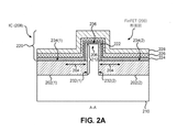
この点に関して、図2Aおよび図2Bは、第1および第2の誘電体材料層202(1)、202(2)を使用してチャネル領域206に応力204を加える例示的なFinFET 200を示す。本明細書で説明するFinFET200は、集積回路(IC)208に組み込むことができる。図2AはFinFET200の断面図であり、図2BはFinFET200の上面図である。FinFET200の構成要素は、図2Aおよび図2Bでは共通の要素番号によって参照されている。
In this regard, FIGS. 2A and 2B show an
図2Aおよび図2Bを参照するとわかるように、FinFET200は、基板210と、基板210から形成されたフィン212とを含む。この例では、フィン212は第1の方向214に配設される。図2Bに示すように、フィン212は、ソース216とドレイン218とを含む。FinFET200のチャネル領域206は、フィン212においてソース216とドレイン218との間に配設される。さらに、チャネル領域206の周りにゲート220が配設される。この例では、ゲート220は、高誘電率金属ゲート(HKMG)として形成される。したがって、以下でより詳細に説明するように、ゲート酸化物層222、ゲート誘電体材料層224、仕事関数層226、および導電層228を使用してゲート220が形成される。しかし、FinFET200の他の態様は、本明細書で説明するHKMG以外のゲートタイプを使用してもよい。さらに、FinFET200はまた、ダミーゲートとして機能するように構成されたゲート構造230(1)〜230(4)を使用することができる。
As can be seen with reference to FIGS. 2A and 2B, the
引き続き図2Aおよび図2Bを参照するとわかるように、チャネル領域206に応力204を加えるために、第1の誘電体材料層202(1)は、基板210の上にかつフィン212の第1の側232(1)に隣接するように配設される。さらに、第2の誘電体材料層202(2)は、基板210の上にかつ第1の側232(1)とは異なるフィン212の第2の側232(2)に隣接するように配設される。この例では、第1および第2の誘電体材料層202(1)、202(2)は第1の方向214に配設される。さらに、第1および第2の誘電体材料層202(1)、202(2)のそれぞれ上面234(1)、234(2)は、ゲート220を形成するための空間を残すようにフィン212の上面236よりも低い。さらに、第1および第2の誘電体材料層202(1)、202(2)は、FinFET200の活性層240を囲む活性領域境界238内に配設される。本明細書で使用するFinFET200の活性層240は、基板210のドープ領域に対応し、ドープ領域上に、FinFET200のソースおよびドレインなどの活性要素が形成される場合がある。このようにして、チャネル領域206に応力204を加え、一方、応力204が加えることができない不活性領域または非ドープ領域に材料を配設するのを回避するように、第1および第2の誘電体材料層202(1)、202(2)を活性領域境界238に限定することができる。
As will continue to be seen with reference to FIGS. 2A and 2B, the first dielectric material layer 202 (1) is placed on top of the
引き続き図2Aおよび図2Bを参照すると、以下でより詳細に説明するように、この態様における第1および第2の誘電体材料層202(1)、202(2)は、流動化学気相堆積(FCVP)または高アスペクト比処理(HARP)などのプロセスを使用して基板210の上に配設された(たとえば、堆積された)1つまたは複数の酸化物材料から形成される。第1および第2の誘電体材料層202(1)、202(2)の酸化物材料は、特定の種類または大きさの応力204を加えるように熱アニールされてもよい。たとえば、第1および第2の誘電体材料層202(1)、202(2)は、二酸化ケイ素またはシリコン窒化物から形成することができる。FinFET200がN型FinFETである場合、第1および第2の誘電体材料層202(1)、202(2)は、チャネル領域206に加えられる応力204が引張応力になるように熱アニールすることができる。FinFET200がP型FinFETである場合、第1および第2の誘電体材料層202(1)、202(2)は、チャネル領域206に加えられる応力204が圧縮応力になるように熱アニールすることができる。
Continuing with reference to FIGS. 2A and 2B, the first and second dielectric material layers 202 (1), 202 (2) in this embodiment are flow chemical vapor deposition (as described in more detail below). It is formed from one or more oxide materials disposed (eg, deposited) on a
図2Aおよび図2Bを引き続き参照するとわかるように、上述のように第1および第2の誘電体材料層202(1)、202(2)の酸化物材料を配設しアニールすることによって、チャネル領域206を含むフィン212に沿って応力204が加えられる。このようにして、エピタキシャル層を成長させることなど、他の方法によって誘起される応力とは異なり、第1および第2の誘電体材料層202(1)、202(2)によって加えられる応力204のレベルは、第1および第2の誘電体材料層202(1)、202(2)の体積に依存しない。より詳細には、第1および第2の誘電体材料層202(1)、202(2)の代わりにエピタキシャル層を使用する例示的なFinFETでは、エピタキシャル層によって加えられる応力の大きさはそのような層の体積と相関する。したがって、そのようなFinFETの面積が狭くなるにつれて、エピタキシャル層によって誘起される応力も弱くなる。このことは、結晶構造の体積が小さくなるにつれてより弱い応力を誘起するエピタキシャル層の結晶構造の特性に起因する。したがって、応力がエピタキシャル層によって誘起される場合とは異なり、第1および第2の誘電体材料層202(1)、202(2)は、FinFET200の面積が狭くなっても、チャネル領域206に一定のレベルの応力204を加えることがある。
Channels are formed by disposing and annealing the oxide materials of the first and second dielectric material layers 202 (1), 202 (2) as described above, as can be seen by continuing to refer to FIGS. 2A and 2B.
さらに、応力が回路内の他のデバイスからFinFET200を電気的に絶縁するために使用されるシャロートレンチ分離(STI)構造242(1)、242(2)を使用することによって誘起される場合とは異なり、第1および第2の誘電体材料層202(1)、202(2)を使用して応力204を加えてもFinFET200の面積は大きくならない。たとえば、STI構造242(1)、242(2)は、各STI構造242(1)、242(2)の幅を大きくすることによって応力を誘起するように設計することができる。STI構造242(1)、242(2)の幅を小さくすると、FinFET200を使用する回路の面積が広くなる。さらに、STI構造242(1)、242(2)の幅を大きくすると、FinFET200に加えられる応力が弱くなる。より詳細には、STI構造242(1)、242(2)によって加えられる応力の大きさは、STI構造242(1)、242(2)の幅と反比例する。したがって、STI構造242(1)、242(2)が拡大すると、その結果加えられる応力が弱くなる。したがって、FinFET200の面積が狭くなっても一定の応力204を加えることに加えて、第1および第2の誘電体材料層202(1)、202(2)は、面積を広くすることなく一定の大きさの応力204を加える。
Furthermore, when stress is induced by using shallow trench isolation (STI) structures 242 (1), 242 (2) used to electrically insulate the
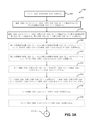
図3Aおよび図3Bは、図2Aおよび図2BにおけるFinFE 200を製作するために使用される例示的な製作プロセス300を示す。さらに、図4A〜図4Dは、製作プロセス300の間のFinFET200のそれぞれの段階400(1)〜400(4)を示す断面図および上面図である。図4A〜図4DにおけるFinFET200を示す断面図および上面図について、図3Aおよび図3Bにおける製作プロセス300の例示的な製作ステップの説明に関連して説明する。
3A and 3B show an
この点に関して、図3Aから始まる製作プロセス300は、フィン212を含む基板210を設ける(ブロック302、図4Aの段階400(1))ことを含む。この例では、フィン212は第1の方向214に配設される。製作プロセス300はまた、基板210の上にかつフィン212の第1の側232(1)に隣接するように第1の誘電体材料層202(1)を配設する(ブロック304、図4Bの段階400(2))ことを含む。製作プロセス300は、基板210の上にかつフィン212の第2の側232(2)に隣接するように第2の誘電体材料層202(2)を配設する(ブロック306、図4Bの段階400(2))ことをさらに含む。この例では、第1および第2の誘電体材料層202(1)、202(2)は第1の方向214に配設される。前述のように、第1および第2の誘電体材料層202(1)、202(2)は、ブロック304および306において流動化学気相堆積(FCVP)または高アスペクト比処理(HARP)などのプロセスを使用して基板210の上に配設することができる。さらに、第1および第2の誘電体材料層202(1)、202(2)は、活性領域境界238に限定されるように配設することができる。
In this regard, the
引き続き図3Aおよび図3Bを参照するとわかるように、熱アニールを使用して、第1および第2の誘電体材料層202(1)、202(2)によって加えられる応力204を調整することができる。より詳細には、製作プロセス300は、第1および第2の誘電体材料層202(1)、202(2)をウェットアニールして、FinFET200のチャネル領域206に加えられる応力204を調整することを含むことができる(ブロック308、図4Bの段階400(2))。たとえば、ブロック308において約600℃の低温ウェットアニールが使用されてもよい。製作プロセス300はまた、第1の誘電体材料層202(1)および第2の誘電体材料層202(2)をドライアニールして、FinFET200のチャネル領域206に加えられる応力204を調整することを含むことができる(ブロック310、図4Bの段階400(2))。たとえば、ブロック310において約1050℃の高温ウェットアニールを使用することができる。
Thermal annealing can be used to adjust the
引き続き図3Aおよび図3Bを参照するとわかるように、製作プロセス300は、ゲート領域406の第1の側404(1)のFinFET200のソース領域402に対応するフィン212をエッチングすることを含むことができる(ブロック312、図4Bの段階400(2))。製作プロセス300はまた、第1の側404(1)とは異なるゲート領域406の第2の側404(2)のFinFET200のドレイン領域408に対応するフィン212をエッチングすることを含むことができる(ブロック314、図4Bの段階400(2))。さらに、製作プロセス300は、ソース領域402においてソース材料410を成長させることを含むことができる(ブロック316、図4Bの段階400(2))。製作プロセス300はまた、ドレイン領域408においてドレイン材料412を成長させることを含むことができる(ブロック318、図4Bの段階400(2))。
As will continue to be seen with reference to FIGS. 3A and 3B, the
引き続き図3Aおよび図3Bを参照するとわかるように、製作プロセス300はまた、FinFET200のゲート長にほぼ等しい幅Wを有するゲート220をゲート領域406内に配設することを含む(ブロック320、図4C、図4Dにおける段階400(3)、400(4))。たとえば、FinFET200が10ナノメートル(nm)技術において使用される場合、ゲート長はほぼ10nmに等しい。詳細には、ゲート220は、フィン212、第1の誘電体材料層202(1)、および第2の誘電体材料層202(2)の上に配設される。この例では、ゲート220は、第1の方向214に実質的に直交する第2の方向414に配設される。ゲート220は、ブロック320において、FinFET200のゲート長にほぼ等しい幅Wを有するゲート酸化物層222をフィン212の上のゲート領域406内に配設することによって配設することができる(ブロック322、図4Cの段階400(3))。ブロック320においてゲート220を配設することは、FinFET200のゲート長にほぼ等しい幅Wを有するゲート誘電体材料層224をゲート領域406内に配設することによって配設することができる(ブロック324、図4Dの段階400(4))。ゲート誘電体材料層224は、ブロック324において、ゲート酸化物層222、第1の誘電体材料層202(1)、および第2の誘電体材料層202(2)の上に配設される。ブロック320においてゲート220を配設することはまた、FinFET200のゲート長にほぼ等しい幅Wを有する仕事関数層226をゲート領域406内に配設することを含むことができる(ブロック326、図4Dの段階400(4))。仕事関数層226は、ゲート誘電体材料層224の上に配設される。さらに、ブロック320においてゲート220を配設することは、FinFET200のゲート長にほぼ等しい幅Wを有する導電層228を仕事関数層226の上のゲート領域406内に配設することを含むことができる(ブロック328、図4Dの段階400(4))。
As will continue to be seen with reference to FIGS. 3A and 3B, the
製作プロセス300を使用してFinFET200を製造すると、FinFET200は、FinFET200の面積が狭くなってもチャネル領域206に一定のレベルの応力204を加えることができる。さらに、製作プロセス300は、従来のFinFET製作方法に含まれる様々なステップを含む。特定の種類または大きさの応力204を誘起するための上記の追加のステップを組み込むと、従来の方法と比較して1つの追加のマスクが含められる場合がある。したがって、上述のように応力204を加え、同時に、製造コストおよび複雑さの増大を最小限に抑えるようにFinFET200を製作することができる。
When the
図2Aおよび図2BにおけるFinFET200に加えて、本明細書で説明する態様はまた、複数のフィンに対応する誘電体材料層を使用して複数のチャネル領域に応力を加えるFinFETを含むことができる。この点に関して、図5Aおよび図5Bは、第1、第2、および第3の誘電体材料層202(1)〜202(3)を使用して第1および第2のチャネル領域206(1)、206(2)に応力204を加える例示的なFinFET500を示す。図5AはFinFET500の断面図であり、図5BはFinFET500の上面図である。FinFET500の構成要素は、図5Aおよび図5Bでは一般的な要素番号によって参照されている。さらに、FinFET500は、図2A、図2Bと図5A、図5Bとの間で同様の要素番号で示されるように、図2Aおよび図2BにおけるFinFET200と共通のいくつかの構成要素を含み、したがって本明細書で再び説明されることはない。
In addition to the
引き続き図5Aおよび図5Bを参照するとわかるように、FinFET500は、基板210と、基板210の上に配設された第1および第2のフィン212(1)、212(2)とを含む。この例では、第1および第2の誘電体材料層212(1)、212(2)は第1の方向214に配設される。非制限的な例として、FinFET500が10nm技術(すなわち、10nmゲート長)において製作される場合、第1および第2のフィン212(1)、212(2)は、32nmにほぼ等しい距離Dだけ分離される。図5Bに示すように、第1および第2のフィン212(1)、212(2)の各々はそれぞれ、ソース216(1)、216(2)とドレイン218(1)、218(2)とを含む。FinFET500の第1および第2のチャネル領域206(1)、206(2)はそれぞれ、第1および第2のフィン212(1)、212(2)において、それぞれのソース216(1)、216(2)とドレイン218(1)、218(2)との間に配設される。さらに、ゲート220は、第1および第2のチャネル領域206(1)、206(2)の周りに配設される。FinFET200と同様に、それぞれ第1および第2のフィン212(1)、212(2)の上のゲート酸化物層222(1)、222(2)、ゲート誘電体材料層224、仕事関数層226、および導電層228を使用してゲート220が形成される。
As will continue to be seen with reference to FIGS. 5A and 5B, the
引き続き図5Aおよび図5Bを参照するとわかるように、FinFET500は、第1のチャネル領域206(1)に応力204を加える第1および第2の誘電体材料層202(1)、202(2)に加えて、チャネル領域206(2)にも応力204が加えられるように設計される。具体的には、第2のフィン212(2)のチャネル領域206(2)に応力204を加えるために、基板210の上にかつ第2のフィン212(2)の第2の側502(2)に隣接するように第3の誘電体材料層202(3)が配設される。さらに、第2の誘電体材料層202(2)は、基板210の上にかつ第2の側502(2)とは異なるフィン212(2)の第2の側502(1)に隣接するように配設される。この例では、第2および第3の誘電体材料層202(2)、202(3)は第1の方向214に配設される。このようにして、第2の誘電体材料層202(2)はまた、チャネル領域206(2)に応力204を加える。さらに、第1、第2、および第3の誘電体材料層202(1)〜202(3)は、FinFET500の活性層506を囲む活性領域境界504内に配設される。したがって、第1、第2、および第3の誘電体材料層202(1)〜202(3)は、FinFET500の面積が狭くなっても、第1および第2のチャネル領域206(1)、206(2)に一定のレベルの応力204を加える場合がある。たとえば、FinFET500の面積が狭くなると、第1のフィン212(1)と第2のフィン212(2)との間の距離Dも32nmよりも短くなる。しかし、上述の第1、第2、および第3の誘電体材料層202(1)〜202(3)の特性に起因して、応力204は、エピタキシャル層によって誘起される応力とは異なり、距離Dが短くなっても一定のままである。
As will continue to be seen with reference to FIGS. 5A and 5B, the
本明細書で説明する要素は、特定の特性を実現するための手段と呼ばれることがある。この点に関して、基板210は、本明細書では「基板を設けるための手段」と呼ばれることがある。フィン212は、本明細書では、「基板の上にフィンを設けるための手段」と呼ばれることがある。さらに、ゲート220は、本明細書では、「チャネル領域の周りにゲートを設けるための手段」と呼ばれることがある。第1の誘電体材料層202(1)は、本明細書では、「基板の上にかつフィンの第1の側に隣接するように第1の誘電体材料層を設けるための手段であって、第1の誘電体材料層がチャネル領域に応力を加える手段」と呼ばれることがある。第2の誘電体材料層202(2)は、本明細書では、「基板の上にかつ第1の側とは異なるフィンの第2の側に隣接するように第2の誘電体材料層を設けるための手段であって、第2の誘電体材料層がチャネル領域に応力を加える手段」と呼ばれることがある。
The elements described herein are sometimes referred to as means for achieving certain properties. In this regard, the
本明細書で開示する態様による、誘電体材料層を使用してチャネル領域に応力を加えるFinFETは、任意のプロセッサベースのデバイス内に設けられるか、またはその中に組み込まれてもよい。例には、限定はしないが、セットトップボックス、エンターテインメントユニット、ナビゲーションデバイス、通信デバイス、固定ロケーションデータユニット、モバイルロケーションデータユニット、全地球測位システム(GPS)デバイス、モバイルフォン、セルラーフォン、スマートフォン、セッション開始プロトコル(SIP)フォン、タブレット、ファブレット、サーバ、コンピュータ、ポータブルコンピュータ、モバイルコンピューティングデバイス、装着型コンピューティングデバイス(たとえば、スマートウォッチ、ヘルスまたはフィットネストラッカー、アイウェアなど)、デスクトップコンピュータ、携帯情報端末(PDA)、モニタ、コンピュータモニタ、テレビ、チューナ、ラジオ、衛星ラジオ、音楽プレーヤ、デジタル音楽プレーヤ、ポータブル音楽プレーヤ、デジタルビデオプレーヤ、ビデオプレーヤ、デジタルビデオディスク(DVD)プレーヤ、ポータブルデジタルビデオプレーヤ、自動車、車両構成要素、アビオニクスシステム、ドローン、およびマルチコプターが含まれる。 A FinFET that stresses the channel region using a dielectric material layer, as disclosed herein, may be provided or incorporated within any processor-based device. Examples include, but are not limited to, set-top boxes, entertainment units, navigation devices, communication devices, fixed location data units, mobile location data units, Global Positioning System (GPS) devices, mobile phones, cellular phones, smartphones, sessions. Initiation Protocol (SIP) Phones, Tablets, Fablets, Servers, Computers, Portable Computers, Mobile Computing Devices, Wearable Computing Devices (eg Smart Watches, Health or Fitness Trackers, Eyewear, etc.), Desktop Computers, Mobile Information Terminal (PDA), monitors, computer monitors, televisions, tuners, radios, satellite radios, music players, digital music players, portable music players, digital video players, video players, digital video disc (DVD) players, portable digital video players, Includes cars, vehicle components, avionics systems, drones, and multicopters.
この点に関して、図6は、図2Aおよび図2Bに示すFinFET200および図5Aおよび図5Bに示すFinFET500を用いることができる、プロセッサベースのシステム600の一例を示す。この例では、プロセッサベースシステム600は、それぞれが1つまたは複数のプロセッサ604を含む、1つまたは複数の中央処理装置(CPU)602を含む。CPU602は、一時的に記憶されたデータへの高速アクセスのためにプロセッサ604に結合されたキャッシュメモリ606を有してもよい。CPU602は、システムバス608に結合され、プロセッサベースシステム600内に含まれるマスタデバイスとスレーブデバイスとを相互結合することができる。よく知られているように、CPU602は、アドレス情報、制御情報、およびデータ情報を、システムバス608を介して交換することによって、これらの他のデバイスと通信する。たとえば、CPU602は、スレーブデバイスの一例として、メモリコントローラ610にバストランザクション要求を通信することができる。図6には示されていないが、複数のシステムバス608を設けることができ、各システムバス608は、異なるファブリックを構成する。
In this regard, FIG. 6 shows an example of a processor-based
他のマスタデバイスおよびスレーブデバイスをシステムバス608に接続することが可能である。図6に示すように、これらのデバイスは、例として、メモリシステム612、1つまたは複数の入力デバイス614、1つまたは複数の出力デバイス616、1つまたは複数のネットワークインターフェースデバイス618、および1つまたは複数のディスプレイコントローラ620を含むことができる。入力デバイス614は、入力キー、スイッチ、音声プロセッサなどを含むが、これらに限定されない、任意のタイプの入力デバイスを含むことができる。出力デバイス616は、オーディオ、ビデオ、他の視覚インジケータなどを含むが、これらに限定されない、任意のタイプの出力デバイスを含むことができる。ネットワークインターフェースデバイス618は、ネットワーク622との間のデータの交換を可能にするように構成された任意のデバイスであってもよい。ネットワーク622は、限定はしないが、有線ネットワークまたはワイヤレスネットワーク、プライベートネットワークまたは公衆ネットワーク、ローカルエリアネットワーク(LAN)、ワイヤレスローカルエリアネットワーク(WLAN)、ワイドエリアネットワーク(WAN)、BLUETOOTH(登録商標)ネットワーク、およびインターネットを含む、任意のタイプのネットワークであってもよい。ネットワークインターフェースデバイス618は、必要に応じて、任意のタイプの通信プロトコルをサポートするように構成されることが可能である。メモリシステム612は、1つまたは複数のメモリユニット624(0)〜624(M)を含むことができる。
Other master and slave devices can be connected to the
CPU602はまた、システムバス608を介してディスプレイコントローラ620にアクセスして、1つまたは複数のディスプレイ626に送信される情報を制御するように構成されてもよい。ディスプレイコントローラ620は、1つまたは複数のビデオプロセッサ628を介して表示されるように情報をディスプレイ626へ送り、ビデオプロセッサ628は、表示すべき情報を処理してディスプレイ626に適したフォーマットにする。ディスプレイ626は、限定はしないが、陰極線管(CRT)、液晶ディスプレイ(LCD)、プラズマディスプレイ、発光ダイオード(LED)ディスプレイなどを含む、任意のタイプのディスプレイを含むことができる。
The
当業者は、本明細書で開示する態様に関して説明する様々な例示的な論理ブロック、モジュール、回路、およびアルゴリズムが、電子ハードウェア、メモリ内もしくは別のコンピュータ可読媒体内に記憶され、プロセッサもしくは他の処理デバイスによって実行される命令、または両方の組合せとして実装され得ることをさらに諒解されよう。本明細書で説明するマスタデバイスおよびスレーブデバイスは、例として、任意の回路、ハードウェア構成要素、集積回路(IC)、またはICチップにおいて採用され得る。本明細書で開示するメモリは、任意のタイプおよびサイズのメモリであってよく、任意のタイプの所望の情報を記憶するように構成され得る。この互換性について明確に例示するために、様々な例示的な構成要素、ブロック、モジュール、回路、およびステップについて、上記では概してそれらの機能に関して説明した。そのような機能性がどのように実装されるのかは、特定の適用例、設計選択、および/またはシステム全体に課される設計制約によって決まる。当業者は、特定の適用例ごとに様々な方式で記載の機能を実装してもよいが、そのような実装の決定が、本開示の範囲からの逸脱を引き起こすと解釈されるべきではない。 Those skilled in the art will appreciate the various exemplary logic blocks, modules, circuits, and algorithms described with respect to the embodiments disclosed herein, stored in electronic hardware, memory, or in another computer-readable medium, processor or other. It will be further understood that it can be implemented as an instruction executed by a processing device of the above, or a combination of both. The master and slave devices described herein can be employed, for example, in any circuit, hardware component, integrated circuit (IC), or IC chip. The memory disclosed herein may be any type and size of memory and may be configured to store any type of desired information. To clearly illustrate this compatibility, various exemplary components, blocks, modules, circuits, and steps have been generally described above with respect to their function. How such functionality is implemented depends on specific application examples, design choices, and / or design constraints imposed on the entire system. One of ordinary skill in the art may implement the features described in various ways for each particular application, but such implementation decisions should not be construed as causing deviations from the scope of the present disclosure.
本明細書で開示する態様に関連して説明した様々な例示的な論理ブロック、モジュール、および回路は、プロセッサ、デジタル信号プロセッサ(DSP)、特定用途向け集積回路(ASIC)、フィールドプログラマブルゲートアレイ(FPGA)もしくは他のプログラマブル論理デバイス、個別ゲートもしくはトランジスタ論理、個別ハードウェア構成要素、または本明細書で説明する機能を実行するように設計されたそれらの任意の組合せを用いて実装または実施されてもよい。プロセッサは、マイクロプロセッサであってもよいが、代替としてプロセッサは、任意の従来のプロセッサ、コントローラ、マイクロコントローラ、またはステートマシンであってもよい。プロセッサはまた、コンピューティングデバイスの組合せ(たとえば、DSPおよびマイクロプロセッサの組合せ、複数のマイクロプロセッサ、DSPコアと連携する1つもしくは複数のマイクロプロセッサ、または任意の他のそのような構成)として実装されてもよい。 The various exemplary logic blocks, modules, and circuits described in relation to the embodiments disclosed herein include processors, digital signal processors (DSPs), application specific integrated circuits (ASICs), and field programmable gate arrays. Implemented or implemented using FPGAs) or other programmable logic devices, individual gate or transistor logic, individual hardware components, or any combination thereof designed to perform the functions described herein. May be good. The processor may be a microprocessor, but instead the processor may be any conventional processor, controller, microcontroller, or state machine. Processors are also implemented as a combination of computing devices (eg, a combination of DSPs and microprocessors, multiple microprocessors, one or more microprocessors working with a DSP core, or any other such configuration). You may.
本明細書で開示する態様は、ハードウェアにおいて具現化されてもよく、かつハードウェア内に記憶され、たとえば、ランダムアクセスメモリ(RAM)、フラッシュメモリ、読取り専用メモリ(ROM)、電気的プログラマブルROM(EPROM)、電気的消去可能プログラマブルROM(EEPROM)、レジスタ、ハードディスク、リムーバブルディスク、CD−ROM、または当技術分野において知られている任意の他の形態のコンピュータ可読媒体の中に存在し得る命令において具現化されてもよい。例示的な記憶媒体は、プロセッサが記憶媒体から情報を読み取るとともに記憶媒体に情報を書き込むことができるように、プロセッサに結合される。代替として、記憶媒体は、プロセッサと一体化してよい。プロセッサおよび記憶媒体は、ASICの中に存在する場合がある。ASICは、リモート局の中に存在する場合がある。代替として、プロセッサおよび記憶媒体は、個別構成要素としてリモート局、基地局、またはサーバの中に存在する場合がある。 The embodiments disclosed herein may be embodied in hardware and are stored in hardware, such as random access memory (RAM), flash memory, read-only memory (ROM), electrically programmable ROM. (EPROM), electrically erasable programmable ROM (EEPROM), registers, hard disks, removable disks, CD-ROMs, or instructions that may be present in any other form of computer-readable medium known in the art. It may be embodied in. An exemplary storage medium is coupled to the processor so that the processor can read information from the storage medium and write information to the storage medium. Alternatively, the storage medium may be integrated with the processor. Processors and storage media may reside in the ASIC. The ASIC may be present in a remote station. Alternatively, the processor and storage medium may reside as individual components within a remote station, base station, or server.
本明細書の例示的な態様のいずれかで説明した動作ステップが、例示および説明のために記載されていることにも留意されたい。説明した動作は、図示のシーケンス以外の数多くの異なるシーケンスにおいて実行される場合がある。さらに、単一の動作ステップにおいて説明する動作は、実際にはいくつかの異なるステップにおいて実行される場合がある。さらに、例示的な態様で説明した1つまたは複数の動作ステップは、組み合わせられてよい。当業者には容易に明らかになるように、フローチャート図に示される動作ステップが数多くの異なる変更を受ける場合があることを理解されたい。情報および信号が様々な異なる技術および技法のいずれかを使用して表される場合があることも当業者は理解されよう。たとえば、上記の説明全体に渡って参照される場合があるデータ、命令、コマンド、情報、信号、ビット、シンボル、およびチップは、電圧、電流、電磁波、磁場もしくは磁気粒子、光場もしくは光学粒子、またはそれらの任意の組合せによって表されてもよい。 It should also be noted that the operating steps described in any of the exemplary embodiments of the present specification are provided for illustration and illustration. The operations described may be performed in a number of different sequences other than those shown. Moreover, the operations described in a single operation step may actually be performed in several different steps. Further, the one or more operation steps described in the exemplary embodiment may be combined. It should be appreciated by those skilled in the art that the operating steps shown in the flow chart are subject to a number of different changes, as will be readily apparent. Those skilled in the art will also appreciate that information and signals may be represented using any of a variety of different techniques and techniques. For example, data, instructions, commands, information, signals, bits, symbols, and chips that may be referred to throughout the above description are voltages, currents, electromagnetic waves, magnetic fields or magnetic particles, light fields or optical particles, Alternatively, it may be represented by any combination thereof.
本開示の上記の説明は、あらゆる当業者が本開示を作成または使用することを可能にするために提供されている。本開示の様々な変更が当業者に容易に明らかになり、本明細書で定義する一般原理は、本開示の趣旨または範囲から逸脱することなく他の変形形態に適用されてもよい。したがって、本開示は、本明細書で説明した例および設計に限定されるものでなく、本明細書で開示する原理および新規の特徴と一致する最も広い範囲を与えられるべきである。 The above description of this disclosure is provided to allow any person skilled in the art to create or use this disclosure. Various modifications of the present disclosure will be readily apparent to those of skill in the art, and the general principles defined herein may be applied to other variants without departing from the spirit or scope of the present disclosure. Accordingly, this disclosure is not limited to the examples and designs described herein, but should be given the broadest scope consistent with the principles and novel features disclosed herein.
100 FinFET
102 基板
104 フィン
106 酸化物層
108 ソース
110 ドレイン
112 伝導チャネル
114 ゲート
116 応力
200 FinFET
202(1)、202(2) 誘電体材料層
204 応力
206 チャネル領域
208 集積回路
210 基板
212 フィン
214 第1の方向
216 ソース
218 ドレイン
220 ゲート
222 ゲート酸化物層
224 ゲート誘電体材料層
226 仕事関数層
228 導電層
230(1)〜230(4) ゲート構造
232(1) 第1の側
232(2) 第2の側
234(1)、234(2) 上面
236 上面
238 活性領域境界
240 活性層
242(1)、242(2) STI構造
404(1) 第1の側
404(2) 第2の側
406 ゲート領域
408 ドレイン領域
410 ソース材料
412 ドレイン材料
414 第2の方向
500 FinFET
502(1) 第1の側
502(2) 第2の側
504 活性領域境界
506 活性層
600 プロセッサベースシステム
602 中央処理装置(CPU)
604 プロセッサ
606 キャッシュメモリ
608 システムバス
610 メモリコントローラ
612 メモリシステム
614 入力デバイス
616 出力デバイス
618 ネットワークインターフェースデバイス
620 ディスプレイコントローラ
622 ネットワーク
624(0)〜624(M) メモリユニット
626 ディスプレイ
628 ビデオプロセッサ
100 FinFET
102
202 (1), 202 (2)
502 (1) 1st side 502 (2) 2nd side 504 Active region boundary 506
604 Processor 606
Claims (13)
基板と、
前記基板の上に配設された第1のフィンであって、
第1のソースと、
第1のドレインと、
前記第1のソースと前記第1のドレインとの間に配設された第1のチャネル領域とを備える第1のフィンと、
前記第1のチャネル領域の周りに配設されたゲートと、
前記基板の上にかつ前記第1のフィンの第1の側の前記第1のチャネル領域に隣接するように配設された第1の誘電体材料層であって、前記第1のチャネル領域に応力を加える第1の誘電体材料層と、
前記基板の上にかつ前記第1の側とは異なる前記第1のフィンの第2の側の前記第1のチャネル領域に隣接するように配設された第2の誘電体材料層であって、前記第1のチャネル領域に応力を加える第2の誘電体材料層と、
前記基板の上にかつ前記第1のフィンに平行に配設された第2のフィンであって、
第2のソースと、
第2のドレインと、
前記第2のフィンの前記第2のソースと前記第2のドレインとの間に配設された第2のチャネル領域とを備える第2のフィンと、
前記第2のフィンの前記第2のチャネル領域の周りに配設された前記ゲートと、
前記基板の上にかつ前記第2のフィンの第2の側の前記第2のチャネル領域に隣接するように配設された第3の誘電体材料層であって、前記第2のフィンの前記第2のチャネル領域に応力を加える第3の誘電体材料層と
を備え、
前記第2の誘電体材料層は、前記第2の誘電体材料層が前記第2のフィンの前記第2のチャネル領域に応力を加えるように、前記基板の上にかつ前記第2の側とは異なる前記第2のフィンの第1の側の前記第2のチャネル領域に隣接するように配設され、
前記第1のフィンと前記第2のフィンとの間の距離が、32ナノメートル以下であり、
前記FinFETの活性層を囲む活性領域境界をさらに備え、前記活性層は、その上に前記ソースおよびドレインが形成された前記基板のドープ領域に対応し、前記第1の誘電体材料層、前記第2の誘電体材料層、および前記第3の誘電体材料層の各々は、前記活性領域境界内のみに配設される、FinFET。 FinFET field effect transistor FinFET
With the board
A first fin disposed on the substrate.
The first source and
With the first drain,
A first fin comprising a first channel region disposed between the first source and the first drain.
With the gates arranged around the first channel region,
A first dielectric material layer disposed on the substrate and adjacent to the first channel region on the first side of the first fin, in the first channel region. The first dielectric material layer to which stress is applied and
A second dielectric material layer disposed on the substrate and adjacent to the first channel region on the second side of the first fin, which is different from the first side. , A second dielectric material layer that stresses the first channel region, and
A second fin disposed on the substrate and parallel to the first fin.
With the second source,
With the second drain,
A second fin comprising a second channel region disposed between the second source of the second fin and the second drain.
With the gate disposed around the second channel region of the second fin,
A third dielectric material layer disposed on the substrate and adjacent to the second channel region on the second side of the second fin, the said second fin. With a third dielectric material layer that stresses the second channel region,
The second dielectric material layer is on and on the second side of the substrate such that the second dielectric material layer stresses the second channel region of the second fin. Are disposed adjacent to the second channel region on the first side of the different second fins.
The distance between the first fin and the second fin is 32 nanometers or less.
Further comprising an active region boundary surrounding the active layer of the FinFET, the active layer corresponds to a dope region of the substrate on which the source and drain are formed, the first dielectric material layer, the first. A FinFET in which each of the second dielectric material layer and the third dielectric material layer is disposed only within the active region boundary.
前記第2の誘電体材料層の上面は、前記第1のフィンの上面よりも低い、請求項1に記載のFinFET。 The upper surface of the first dielectric material layer is lower than the upper surface of the first fin.
The FinFET according to claim 1, wherein the upper surface of the second dielectric material layer is lower than the upper surface of the first fin.
前記第1および第2の誘電体材料層は、前記第1および第2の誘電体材料層が前記第1のチャネル領域に引張応力を加えるように1つまたは複数の酸化物材料を含む、請求項1に記載のFinFET。 The FinFET includes an N-type FinFET.
The first and second dielectric material layers are claimed to include one or more oxide materials such that the first and second dielectric material layers apply tensile stress to the first channel region. Item 1. The FinFET according to Item 1.
前記第1および第2の誘電体材料層は、前記第1および第2の誘電体材料層が前記第1のチャネル領域に圧縮応力を加えるように1つまたは複数の酸化物材料を含む、請求項1に記載のFinFET。 The FinFET includes a P-type FinFET.
The first and second dielectric material layers are claimed to include one or more oxide materials such that the first and second dielectric material layers apply compressive stress to the first channel region. Item 1. The FinFET according to Item 1.
第1のフィンおよび第2のフィンを備える基板を設けるステップであって、前記第1のフィンは、第1のソースと、第1のドレインと、前記第1のソースと前記第1のドレインとの間に配設された第1のチャネル領域とを備え、前記第2のフィンは、第2のソースと、第2のドレインと、前記第2のソースと前記第2のドレインとの間に配設された第2のチャネル領域とを備える、ステップと、
前記基板の上にかつ前記第1のフィンの第1の側の前記チャネル領域に隣接するように第1の誘電体材料層を配設するステップと、
前記基板の上にかつ前記第1のフィンの第2の側の前記チャネル領域に隣接するように第2の誘電体材料層を配設するステップであって、前記第2の側が前記第1の側とは異なる、ステップと、
前記第1のフィン、前記第2のフィン、前記第1の誘電体材料層、および前記第2の誘電体材料層の上のゲート領域内に、前記FinFETのゲート長に等しい幅を有するゲートを配設するステップとを含み、
前記第1のフィンと前記第2のフィンとの間の距離が、32ナノメートル以下であり、
前記第1の誘電体材料層を配設する前記ステップは、前記基板の上に、かつ前記FinFETの活性層を囲む活性領域境界内のみに、前記第1のフィンの第1の側の前記チャネル領域に隣接するように前記第1の誘電体材料層を配設するステップであって、前記活性層は、その上に前記ソースおよびドレインが形成された前記基板のドープ領域に対応する、ステップを含み、
前記第2の誘電体材料層を配設する前記ステップは、前記基板の上に、かつ前記活性領域境界内のみに、前記第1のフィンの前記第2の側の前記チャネル領域に隣接するように前記第2の誘電体材料層を配設するステップを含む、方法。 A method for making a fin field effect transistor FinFET that applies stress to the channel region using a dielectric material layer.
A step of providing a substrate comprising a first fin and a second fin, wherein the first fin includes a first source, a first drain, the first source, and the first drain. The second fin comprises a first channel region disposed between the two sources, the second source, the second drain, and the second source and the second drain. A step, comprising a second channel region disposed.
A step of disposing a first dielectric material layer on the substrate and adjacent to the channel region on the first side of the first fin.
A step of disposing a second dielectric material layer on the substrate and adjacent to the channel region on the second side of the first fin, wherein the second side is the first. Different from the side, with steps,
A gate having a width equal to the gate length of the FinFET in the gate region above the first fin, the second fin, the first dielectric material layer, and the second dielectric material layer. Including steps to dispose
The distance between the first fin and the second fin is 32 nanometers or less.
The step of disposing the first dielectric material layer is on the substrate and only within the active region boundary surrounding the active layer of the FinFET, the channel on the first side of the first fin. A step of disposing the first dielectric material layer adjacent to the region, wherein the active layer corresponds to a dope region of the substrate on which the source and drain are formed. Including,
The step of disposing the second dielectric material layer is such that it is adjacent to the channel region on the second side of the first fin only on the substrate and within the active region boundary. A method comprising the step of disposing the second dielectric material layer.
前記FinFETのゲート長に等しい幅を有するゲート酸化物層を前記第1のフィンおよび前記第2のフィンの上の前記ゲート領域内に配設するステップと、
前記ゲート酸化物層、前記第1の誘電体材料層、および前記第2の誘電体材料層の上のゲート領域内に、前記FinFETの前記ゲート長に等しい幅を有するゲート誘電体材料層を配設するステップと、
前記ゲート誘電体材料層の上の前記ゲート領域内に、前記FinFETの前記ゲート長に等しい幅を有する仕事関数層を配設するステップと、
前記仕事関数層の上の前記ゲート領域内に、前記FinFETの前記ゲート長に等しい幅を有する導電層を配設するステップとを含む、請求項6に記載の方法。 The step of arranging the gate is
A step of disposing a gate oxide layer having a width equal to the gate length of the FinFET in the gate region on the first fin and the second fin.
Within the gate region above the gate oxide layer, the first dielectric material layer, and the second dielectric material layer, a gate dielectric material layer having a width equal to the gate length of the FinFET is arranged. Steps to set up and
A step of disposing a work function layer having a width equal to the gate length of the FinFET in the gate region on the gate dielectric material layer.
The method of claim 6 , comprising the step of disposing a conductive layer having a width equal to the gate length of the FinFET in the gate region above the work function layer.
前記ゲート領域の第1の側とは異なる前記ゲート領域の第2の側の前記FinFETのドレイン領域に対応する前記第1のフィンをエッチングするステップと、
前記ソース領域においてソース材料を成長させるステップと、
前記ドレイン領域内でドレイン材料を成長させるステップとをさらに含む、請求項6に記載の方法。 A step of etching the first fin corresponding to the source region of the FinFET on the first side of the gate region.
A step of etching the first fin corresponding to the drain region of the FinFET on the second side of the gate region, which is different from the first side of the gate region.
The step of growing the source material in the source region,
The method of claim 6 , further comprising the step of growing the drain material in the drain region.
前記第2の誘電体材料層を配設する前記ステップは、流動化学気相堆積を使用して前記基板の上にかつ前記第1のフィンの前記第2の側の前記チャネル領域に隣接するように前記第2の誘電体材料層を配設するステップを含む、請求項6に記載の方法。 The step of disposing the first dielectric material layer is such that the flow chemical vapor deposition is used on the substrate and adjacent to the channel region on the first side of the first fin. Including the step of disposing the first dielectric material layer in the
The step of disposing the second dielectric material layer is such that the flow chemical vapor deposition is used on the substrate and adjacent to the channel region on the second side of the first fin. 6. The method of claim 6 , comprising the step of disposing the second dielectric material layer.
前記第2の誘電体材料層を配設する前記ステップは、流動化学気相堆積を使用して前記基板の上にかつ前記第1のフィンの前記第2の側に隣接するように1つまたは複数の酸化物材料を配設するステップを含む、請求項6に記載の方法。 The step of disposing the first dielectric material layer may be one or the other so as to be on the substrate and adjacent to the first side of the first fin using flow chemical vapor deposition. Including the step of disposing multiple oxide materials
The step of disposing the second dielectric material layer may be one or the other so as to be on the substrate and adjacent to the second side of the first fin using flow chemical vapor deposition. The method of claim 6 , comprising the step of disposing the plurality of oxide materials.
前記第2の誘電体材料層を配設する前記ステップは、高アスペクト比処理を使用して前記基板の上にかつ前記第1のフィンの前記第2の側の前記チャネル領域に隣接するように1つまたは複数の酸化物材料を配設するステップを含む、請求項6に記載の方法。 The step of disposing the first dielectric material layer is such that the high aspect ratio treatment is used on the substrate and adjacent to the channel region on the first side of the first fin. Including the step of disposing one or more oxide materials
The step of disposing the second dielectric material layer is such that the high aspect ratio treatment is used on the substrate and adjacent to the channel region on the second side of the first fin. The method of claim 6 , comprising the step of disposing one or more oxide materials.
Applications Claiming Priority (3)
| Application Number | Priority Date | Filing Date | Title |
|---|---|---|---|
| US15/266,840 | 2016-09-15 | ||
| US15/266,840 US9882051B1 (en) | 2016-09-15 | 2016-09-15 | Fin field effect transistors (FETs) (FinFETs) employing dielectric material layers to apply stress to channel regions |
| PCT/US2017/046525 WO2018052591A1 (en) | 2016-09-15 | 2017-08-11 | Fin field effect transistors (fets) (finfets) employing dielectric material layers to apply stress to channel regions |
Publications (3)
| Publication Number | Publication Date |
|---|---|
| JP2019530227A JP2019530227A (en) | 2019-10-17 |
| JP2019530227A5 JP2019530227A5 (en) | 2020-08-27 |
| JP6974446B2 true JP6974446B2 (en) | 2021-12-01 |
Family
ID=59684098
Family Applications (1)
| Application Number | Title | Priority Date | Filing Date |
|---|---|---|---|
| JP2019513978A Active JP6974446B2 (en) | 2016-09-15 | 2017-08-11 | Fin field effect transistor (FET) that applies stress to the channel region using a dielectric material layer |
Country Status (8)
| Country | Link |
|---|---|
| US (1) | US9882051B1 (en) |
| EP (1) | EP3513437A1 (en) |
| JP (1) | JP6974446B2 (en) |
| KR (1) | KR102550579B1 (en) |
| CN (1) | CN109844957A (en) |
| BR (1) | BR112019004507B1 (en) |
| CA (1) | CA3032965A1 (en) |
| WO (1) | WO2018052591A1 (en) |
Families Citing this family (2)
| Publication number | Priority date | Publication date | Assignee | Title |
|---|---|---|---|---|
| US10109507B2 (en) * | 2016-06-01 | 2018-10-23 | Taiwan Semiconductor Manufacturing Co., Ltd. | Fluorine contamination control in semiconductor manufacturing process |
| US11211243B2 (en) * | 2018-11-21 | 2021-12-28 | Taiwan Semiconductor Manufacturing Company, Ltd. | Method of filling gaps with carbon and nitrogen doped film |
Family Cites Families (20)
| Publication number | Priority date | Publication date | Assignee | Title |
|---|---|---|---|---|
| US7081395B2 (en) | 2003-05-23 | 2006-07-25 | Taiwan Semiconductor Manufacturing Co., Ltd. | Silicon strain engineering accomplished via use of specific shallow trench isolation fill materials |
| JP2007207837A (en) | 2006-01-31 | 2007-08-16 | Toshiba Corp | Semiconductor device, and method of manufacturing same |
| US7939862B2 (en) | 2007-05-30 | 2011-05-10 | Synopsys, Inc. | Stress-enhanced performance of a FinFet using surface/channel orientations and strained capping layers |
| US7943531B2 (en) * | 2007-10-22 | 2011-05-17 | Applied Materials, Inc. | Methods for forming a silicon oxide layer over a substrate |
| US7915112B2 (en) | 2008-09-23 | 2011-03-29 | Taiwan Semiconductor Manufacturing Company, Ltd. | Metal gate stress film for mobility enhancement in FinFET device |
| US9953885B2 (en) * | 2009-10-27 | 2018-04-24 | Taiwan Semiconductor Manufacturing Company, Ltd. | STI shape near fin bottom of Si fin in bulk FinFET |
| US8426923B2 (en) * | 2009-12-02 | 2013-04-23 | Taiwan Semiconductor Manufacturing Company, Ltd. | Multiple-gate semiconductor device and method |
| DE102010002410B4 (en) | 2010-02-26 | 2017-03-02 | Globalfoundries Dresden Module One Limited Liability Company & Co. Kg | Deformation memory technology in deformed SOI substrates of semiconductor devices |
| US8937353B2 (en) * | 2010-03-01 | 2015-01-20 | Taiwan Semiconductor Manufacturing Co., Ltd. | Dual epitaxial process for a finFET device |
| JP2013093438A (en) * | 2011-10-26 | 2013-05-16 | Renesas Electronics Corp | Semiconductor device manufacturing method |
| US8698199B2 (en) | 2012-01-11 | 2014-04-15 | United Microelectronics Corp. | FinFET structure |
| US8941187B2 (en) | 2012-01-13 | 2015-01-27 | Globalfoundries Inc. | Strain engineering in three-dimensional transistors based on strained isolation material |
| CN103681846B (en) | 2012-09-20 | 2017-02-08 | 中芯国际集成电路制造(上海)有限公司 | Semiconductor device and manufacturing method thereof |
| US9263585B2 (en) * | 2012-10-30 | 2016-02-16 | Globalfoundries Inc. | Methods of forming enhanced mobility channel regions on 3D semiconductor devices, and devices comprising same |
| US8759874B1 (en) * | 2012-11-30 | 2014-06-24 | Stmicroelectronics, Inc. | FinFET device with isolated channel |
| US8877588B2 (en) | 2013-02-11 | 2014-11-04 | Globalfoundries Inc. | Methods of forming a three-dimensional semiconductor device with a dual stress channel and the resulting device |
| US9721955B2 (en) | 2014-04-25 | 2017-08-01 | Taiwan Semiconductor Manufacturing Company, Ltd. | Structure and method for SRAM FinFET device having an oxide feature |
| US9306067B2 (en) | 2014-08-05 | 2016-04-05 | Taiwan Semiconductor Manufacturing Company, Ltd. | Nonplanar device and strain-generating channel dielectric |
| TWI655774B (en) * | 2015-08-12 | 2019-04-01 | 聯華電子股份有限公司 | Semiconductor device and method for fabricating the same |
| US9614086B1 (en) * | 2015-12-30 | 2017-04-04 | Taiwan Semiconductor Manufacturing Company, Ltd. | Conformal source and drain contacts for multi-gate field effect transistors |
-
2016
- 2016-09-15 US US15/266,840 patent/US9882051B1/en active Active
-
2017
- 2017-08-11 JP JP2019513978A patent/JP6974446B2/en active Active
- 2017-08-11 KR KR1020197007266A patent/KR102550579B1/en active IP Right Grant
- 2017-08-11 CN CN201780056420.3A patent/CN109844957A/en active Pending
- 2017-08-11 CA CA3032965A patent/CA3032965A1/en active Pending
- 2017-08-11 EP EP17755390.6A patent/EP3513437A1/en active Pending
- 2017-08-11 BR BR112019004507-4A patent/BR112019004507B1/en active IP Right Grant
- 2017-08-11 WO PCT/US2017/046525 patent/WO2018052591A1/en active Search and Examination
Also Published As
| Publication number | Publication date |
|---|---|
| CN109844957A (en) | 2019-06-04 |
| EP3513437A1 (en) | 2019-07-24 |
| KR102550579B1 (en) | 2023-07-03 |
| WO2018052591A1 (en) | 2018-03-22 |
| KR20190047696A (en) | 2019-05-08 |
| CA3032965A1 (en) | 2018-03-22 |
| BR112019004507B1 (en) | 2023-10-03 |
| BR112019004507A2 (en) | 2019-06-04 |
| US9882051B1 (en) | 2018-01-30 |
| JP2019530227A (en) | 2019-10-17 |
Similar Documents
| Publication | Publication Date | Title |
|---|---|---|
| US10134734B2 (en) | Fin field effect transistor (FET) (FinFET) complementary metal oxide semiconductor (CMOS) circuits employing single and double diffusion breaks for increased performance | |
| US9570442B1 (en) | Applying channel stress to Fin field-effect transistors (FETs) (FinFETs) using a self-aligned single diffusion break (SDB) isolation structure | |
| US20210050455A1 (en) | Fabrication of non-planar igzo devices for improved electrostatics | |
| US10032678B2 (en) | Nanowire channel structures of continuously stacked nanowires for complementary metal oxide semiconductor (CMOS) devices | |
| JP2016516301A (en) | Metal oxide semiconductor (MOS) isolation scheme and related methods having continuous active regions divided by dummy gates | |
| JP6974446B2 (en) | Fin field effect transistor (FET) that applies stress to the channel region using a dielectric material layer | |
| US20200273998A1 (en) | Source electrode and drain electrode protection for nanowire transistors | |
| US10714582B2 (en) | Controlling dimensions of a negative capacitance layer of a gate stack of a field-effect transistor (FET) to increase power density | |
| EP3378095B1 (en) | Semiconductor devices with wider field gates for reduced gate resistance | |
| US20170084628A1 (en) | Substrate-transferred, deep trench isolation silicon-on-insulator (soi) semiconductor devices formed from bulk semiconductor wafers | |
| US9171952B2 (en) | Low gate-to-drain capacitance fully merged finFET | |
| TWI721110B (en) | Nanowire for transistor integration | |
| US11798838B2 (en) | Capacitance reduction for semiconductor devices based on wafer bonding | |
| US20190296126A1 (en) | Systems and methods for dummy gate tie-offs in a self-aligned gate contact (sagc) cell | |
| US20150311138A1 (en) | Transistors with improved thermal conductivity | |
| EP3513429B1 (en) | Semiconductor devices employing field effect transistors (fets) with multiple channel structures without shallow trench isolation (sti) void-induced electrical shorts | |
| TWI836013B (en) | Gate stacks for finfet transistors | |
| US10600774B2 (en) | Systems and methods for fabrication of gated diodes with selective epitaxial growth | |
| US11532719B2 (en) | Transistors on heterogeneous bonding layers |
Legal Events
| Date | Code | Title | Description |
|---|---|---|---|
| A521 | Request for written amendment filed |
Free format text: JAPANESE INTERMEDIATE CODE: A523 Effective date: 20190318 |
|
| A521 | Request for written amendment filed |
Free format text: JAPANESE INTERMEDIATE CODE: A523 Effective date: 20200717 |
|
| A621 | Written request for application examination |
Free format text: JAPANESE INTERMEDIATE CODE: A621 Effective date: 20200717 |
|
| A131 | Notification of reasons for refusal |
Free format text: JAPANESE INTERMEDIATE CODE: A131 Effective date: 20210531 |
|
| A977 | Report on retrieval |
Free format text: JAPANESE INTERMEDIATE CODE: A971007 Effective date: 20210531 |
|
| A521 | Request for written amendment filed |
Free format text: JAPANESE INTERMEDIATE CODE: A523 Effective date: 20210831 |
|
| TRDD | Decision of grant or rejection written | ||
| A01 | Written decision to grant a patent or to grant a registration (utility model) |
Free format text: JAPANESE INTERMEDIATE CODE: A01 Effective date: 20211004 |
|
| A61 | First payment of annual fees (during grant procedure) |
Free format text: JAPANESE INTERMEDIATE CODE: A61 Effective date: 20211104 |
|
| R150 | Certificate of patent or registration of utility model |
Ref document number: 6974446 Country of ref document: JP Free format text: JAPANESE INTERMEDIATE CODE: R150 |