JP6972575B2 - Frequency characteristic adjustment circuit, optical transmission module using this, and optical transceiver - Google Patents
Frequency characteristic adjustment circuit, optical transmission module using this, and optical transceiver Download PDFInfo
- Publication number
- JP6972575B2 JP6972575B2 JP2017030312A JP2017030312A JP6972575B2 JP 6972575 B2 JP6972575 B2 JP 6972575B2 JP 2017030312 A JP2017030312 A JP 2017030312A JP 2017030312 A JP2017030312 A JP 2017030312A JP 6972575 B2 JP6972575 B2 JP 6972575B2
- Authority
- JP
- Japan
- Prior art keywords
- circuit
- current
- optical
- signal
- drive
- Prior art date
- Legal status (The legal status is an assumption and is not a legal conclusion. Google has not performed a legal analysis and makes no representation as to the accuracy of the status listed.)
- Active
Links
Images


Landscapes
- Optical Modulation, Optical Deflection, Nonlinear Optics, Optical Demodulation, Optical Logic Elements (AREA)
- Optical Communication System (AREA)
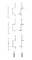
Description
本発明は、周波数特性調整回路とこれを用いた光送信モジュール、及び光トランシーバに関する。 The present invention relates to a frequency characteristic adjustment circuit, an optical transmission module using the same, and an optical transceiver.
データトラフィックの増大に伴い、光通信ネットワークの大容量化のため1波長あたり40Gbps(ギガビット毎秒)、100Gbpsなどの高速通信が実用化されつつある。高速の光通信を実現する技術のひとつとして、シリコンフォトニクス技術で微細な光導波路構造を作製し、1チップに演算回路と電気/光変換回路を集積する技術が注目されている。シリコンフォトニクスの光変調器では、導波路の中央に形成されたPN接合に電圧を印加し、キャリア密度の変化すなわち屈折率の変化(キャリアプラズマ分散)を利用して光路長を変化させる。屈折率の変化はキャリア密度の変化に比例するため、できるだけ小さな電圧変化でキャリア密度を変化させることが望ましい。PN接合では順方向にバイアス電圧を印加したときのほうがキャリア密度の変化が大きく、変調効率がよい。しかし、それゆえに帯域が狭いという問題がある。ドライバ側から見ると、光変調器の接合容量は負荷容量に見え、高周波成分の信号が減衰して帯域が劣化するからである。pin型ダイオードを用いた場合は接合容量がより大きいため、高周波帯域での特性が悪くなる。 With the increase in data traffic, high-speed communication such as 40 Gbps (gigabit per second) and 100 Gbps per wavelength is being put into practical use in order to increase the capacity of optical communication networks. As one of the technologies for realizing high-speed optical communication, a technology for producing a fine optical waveguide structure by silicon photonics technology and integrating an arithmetic circuit and an electric / optical conversion circuit on one chip is attracting attention. In the silicon photonics light modulator, a voltage is applied to the PN junction formed in the center of the waveguide, and the optical path length is changed by utilizing the change in carrier density, that is, the change in refractive index (carrier plasma dispersion). Since the change in the refractive index is proportional to the change in the carrier density, it is desirable to change the carrier density with the smallest possible voltage change. In the PN junction, the change in carrier density is larger and the modulation efficiency is better when the bias voltage is applied in the forward direction. However, there is a problem that the band is narrow. From the driver's point of view, the junction capacitance of the light modulator looks like a load capacitance, and the signal of the high frequency component is attenuated and the band deteriorates. When a pin type diode is used, the junction capacitance is large, so that the characteristics in the high frequency band are deteriorated.
高速駆動される光変調器で帯域の劣化を防止する方法として、ドライバ回路と光変調器の間に、キャパシタ(C)と抵抗(R)で形成される整合回路(マッチング回路)を挿入する方法が提案されている(たとえば、非特許文献1参照)。光変調器のPN接合と電気的に等価な整合回路を挿入することで、pin型ダイオードの接合容量を光変調器の設計容量に低減する。 As a method of preventing band deterioration in a high-speed driven optical modulator, a matching circuit (matching circuit) formed by a capacitor (C) and a resistor (R) is inserted between the driver circuit and the optical modulator. Has been proposed (see, for example, Non-Patent Document 1). By inserting a matching circuit that is electrically equivalent to the PN junction of the optical modulator, the junction capacitance of the pin type diode is reduced to the design capacitance of the optical modulator.
駆動回路と光変調器、面発光レーザ等の光回路素子の間にイコライズ回路を挿入して、高周波側に帯域拡張する構成を採用した場合、入力データパタン(「1」または「0」)に応じた光回路出力を得るために、大きな駆動電圧が必要になる。たとえば、シリコンフォトニクスで形成された光変調器を駆動する現実的な電圧値(VDD)では、イコライズ回路が挿入された光変調器回路を高速駆動して入力データパタンに応じた変調器出力を得ることが難しい。 When an equalization circuit is inserted between the drive circuit and an optical circuit element such as an optical modulator or a surface emission laser to expand the band to the high frequency side, the input data pattern (“1” or “0”) is used. A large drive voltage is required to obtain the corresponding optical circuit output. For example, in a realistic voltage value (VDD ) that drives an optical modulator formed of silicon photonics, the optical modulator circuit with an equalize circuit inserted is driven at high speed to output the modulator output according to the input data pattern. Difficult to get.
そこで、低い電圧で光回路素子を高速駆動し、応答特性の良い光出力を得ることのできる構成を提供することを目的とする。 Therefore, it is an object of the present invention to provide a configuration capable of driving an optical circuit element at a high speed with a low voltage and obtaining an optical output having good response characteristics.
本発明の一態様では、光回路素子と前記光回路素子を駆動する駆動回路の間に周波数特性調整回路が配置され、前記周波数特性調整回路は、
前記駆動回路の出力に接続されるキャパシタと、
前記駆動回路で生成される電圧によって制御される電流供給回路と、を有し、
前記電流供給回路は、前記駆動回路から受け取る電圧に応じて異なる電流値の電流を前記光回路素子に供給する。
In one aspect of the present invention, a frequency characteristic adjusting circuit is arranged between the optical circuit element and the drive circuit for driving the optical circuit element, and the frequency characteristic adjusting circuit is the frequency characteristic adjusting circuit.
The capacitor connected to the output of the drive circuit and
It has a current supply circuit, which is controlled by the voltage generated by the drive circuit, and
The current supply circuit supplies the optical circuit element with a current having a different current value depending on the voltage received from the drive circuit.
上記の構成により、低い電圧で光回路素子を高速駆動して良好な応答特性を得ることができる。 With the above configuration, it is possible to drive the optical circuit element at high speed with a low voltage and obtain good response characteristics.
実施形態では、ドライバ(駆動回路)と光変調器等の光回路素子の間に、キャパシタと電流源を含む周波数特性調整回路を挿入する。周波数特性調整回路の挿入により、帯域を拡張し、駆動電圧を増大させずに、あるいは高電圧源や負電圧源を追加せずに、高速駆動で入力データパタンに応じた光出力を得る。周波数特性調整回路は、ドライバからの出力電圧に応じて電流源から光回路素子へ供給される電流量を調整する。この構成により、低い電圧で光回路素子を高速駆動し、かつ、光回路素子の応答特性を安定させることができる。中周波数から高周波の領域で周波数特性が安定するため、副次的な効果として符号間干渉を抑制することができる。実施形態の構成の詳細を説明する前に、公知文献のマッチング回路の構成をそのまま適用したイコライズ回路を挿入することによる帯域の拡張とその問題点を説明する。 In the embodiment, a frequency characteristic adjustment circuit including a capacitor and a current source is inserted between the driver (drive circuit) and an optical circuit element such as an optical modulator. By inserting the frequency characteristic adjustment circuit, the band is expanded and the optical output according to the input data pattern is obtained by high-speed driving without increasing the driving voltage or adding a high voltage source or a negative voltage source. The frequency characteristic adjustment circuit adjusts the amount of current supplied from the current source to the optical circuit element according to the output voltage from the driver. With this configuration, the optical circuit element can be driven at high speed with a low voltage, and the response characteristics of the optical circuit element can be stabilized. Since the frequency characteristics are stable in the medium to high frequency range, intersymbol interference can be suppressed as a secondary effect. Before explaining the details of the configuration of the embodiment, the band expansion by inserting the equalization circuit to which the configuration of the matching circuit of the publicly known document is applied as it is and the problem thereof will be described.
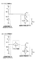
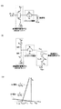
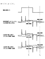
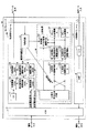
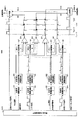
図1と図2は、イコライズ回路の挿入による帯域の拡張を説明する図である。図1(A)はイコライズ回路なしの駆動回路と光変調器の等価回路図、図1(B)はイコライズ回路を挿入したときの等価回路図である。 1 and 2 are diagrams for explaining band expansion by inserting an equalize circuit. FIG. 1A is an equivalent circuit diagram of a drive circuit without an equalizing circuit and an optical modulator, and FIG. 1B is an equivalent circuit diagram when an equalizing circuit is inserted.
光変調器を駆動するCMOSドライバの各MOSトランジスタは、スイッチ(SW)と内部抵抗(RL)で表され、VDDとVSSの間に直列接続されている。イコライズ回路は、並列接続される抵抗RFとキャパシタンスCFで表される。光変調器は、並列接続される接合容量CM及び接合抵抗RMと、直列の寄生抵抗Rsで表される。VMODは光変調器の容量部分にかかる電圧である。 Each MOS transistor of the CMOS driver for driving the optical modulator is represented by the switch (SW) and internal resistance (R L), connected in series between V DD and V SS. Equalizing circuit is represented by a resistor R F and the capacitance C F are connected in parallel. Optical modulator, a junction capacitance C M and the junction resistance R M are connected in parallel, is represented by the series parasitic resistor Rs. V MOD is the voltage applied to the capacitive portion of the light modulator.
図1(A)でイコライズ回路なしの場合、光変調器の容量部分に加わる電圧VMOD(正確には電圧VMODでの電荷量)は位相変化量に比例し、電圧VMODの周波数依存性は光変調器の周波数依存性を表わす。図1(A)の構成で、電圧VMODの周波数依存性は、式(1)で表される。 When there is no equalization circuit in FIG. 1 (A), the voltage V MOD (more accurately, the amount of charge in the voltage V MOD ) applied to the capacitive portion of the optical modulator is proportional to the amount of phase change, and the frequency dependence of the voltage V MOD. Represents the frequency dependence of the light modulator. In the configuration of FIG. 1A, the frequency dependence of the voltage V MOD is expressed by the equation (1).
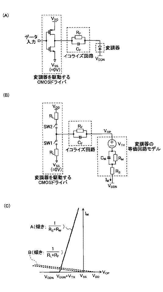
図1(B)でイコライズ回路が挿入された場合、イコライズ回路の抵抗RFとキャパシタンスCFが加わり、電圧条件は式(2)で表される。 If the equalizing circuit is inserted in FIG. 1 (B), the added resistance R F and the capacitance C F of the equalizing circuit, the voltage condition is expressed by Equation (2).
CMRM=CFRFが成り立つときは、式(2)は式(3)となり、式(1)と同じ形になる。 When C M R M = C F R F , the equation (2) becomes the equation (3) and has the same form as the equation (1).
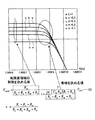
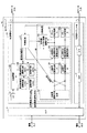
図2は、周波数特性とイコライズ回路の抵抗RFの関係を示す。グラフの横軸は周波数[Hz]、縦軸はゲインまたは光変調器にかかる電圧である。パラメータηを、
η=(RL+RS+RM)/(RL+RS+RM+RF)
として、イコライズ回路のないとき(RF=0すなわちη=1)とイコライズ回路を挿入したとき(η<1)を比較する。式(3)の右辺で乗算される最初の項のRM/(RL+RS+RM+RF)が低周波領域の利得を決める項であり、CMRM(RL+RS)/(RL+RS+RM+RF)が帯域を決める項である。
Figure 2 shows the relationship between the resistance R F of the frequency response and equalizing circuit. The horizontal axis of the graph is the frequency [Hz], and the vertical axis is the gain or voltage applied to the light modulator. Parameter η,
η = ( RL + R S + RM ) / ( RL + R S + R M + R F )
As is compared in the absence of the equalizing circuit and (R F = 0 i.e. eta = 1) upon insertion of the equalizing circuit (η <1). The first term RM / ( RL + R S + R M + R F ) multiplied by the right-hand side of equation (3) is the term that determines the gain in the low frequency region, and is C M R M ( RL + R S ) /. ( RL + R S + R M + R F ) is a term that determines the band.
イコライズ回路を挿入することで、中周波数領域の利得はフラットな特性を維持したまま「η」の値に応じて下がるが、帯域は1/η倍に拡張されることがわかる。また、CMRM=CFRFのときには、RFの調整だけで低周波領域の利得と、帯域を制御できることがわかる。 It can be seen that by inserting the equalize circuit, the gain in the middle frequency region decreases according to the value of "η" while maintaining the flat characteristics, but the band is expanded by 1 / η times. Further, when C M R M = C F R F , it can be seen that the gain and band in the low frequency region can be controlled only by adjusting the R F.
図1及び図2の説明は、駆動対象が光変調器である場合に限らず、たとえば直接駆動型のレーザダイオードを駆動する場合にも当てはまる。 The description of FIGS. 1 and 2 applies not only to the case where the driving target is an optical modulator, but also to the case of driving, for example, a direct drive type laser diode.
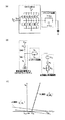
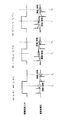
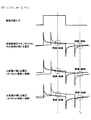
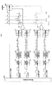
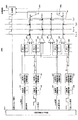
図3は、イコライズ回路を用いるときの課題を説明する図である。図3(A)は駆動回路をCMOSドライバで形成し、CMOSドライバとダイオードの間にイコライズ回路を挿入した図を示す。イコライズ回路の容量のコンダクタンスをηCON、抵抗のコンダクタンスをηGONとする。ドライバ側からみると、総容量はηCON/(1+η)となる。ηを1より十分に小さくすれば容量が小さくなり、高速動作でも周波数依存性が小さくなる。これは図2でも示されるとおりである。 FIG. 3 is a diagram illustrating a problem when using an equalize circuit. FIG. 3A shows a diagram in which a drive circuit is formed by a CMOS driver and an equalize circuit is inserted between the CMOS driver and a diode. ItaC ON the conductance of the capacity of the equalizing circuit, the conductance of the resistor and ηG ON. Seen from the driver side, the total capacity is ηC ON / (1 + η). If η is made sufficiently smaller than 1, the capacitance becomes small, and the frequency dependence becomes small even in high-speed operation. This is also shown in FIG.
図3(B)は、図3(A)に対応する等化回路モデルである。CMOSドライバのトランジスタは、スイッチSWと内部抵抗RLで単純化されている。図3(C)のグラフの横軸は動作電圧VOP、縦軸は光変調器に流れる電流IMである。実線Aは光変調器の電流-電圧特性、破線Bは負荷線を示す。たとえば、ドライバが高電位(H)側の電圧を出力するときに変調器が「1」の状態を出力するためには、適切なRLまたは電源電圧VDDを与える必要がある。閾値電圧VTHが0.6V、電流-電圧特性と負荷線の交点を0.9V(オーバードライバ電圧は0.3V)、η=0.1(10倍の帯域拡大)とする。この場合、RLを無限大、RSを0に近似したとしてもVDDは3.6Vとなる。このような電圧が可能なCMOSでドライバ回路を作製しても、10Gbps以上の高速で動作させることはできない。 FIG. 3B is an equalization circuit model corresponding to FIG. 3A. The CMOS driver transistor is simplified with a switch SW and an internal resistance RL. The horizontal axis operating voltage V OP of the graph of FIG. 3 (C), the vertical axis represents the current I M flowing through the optical modulator. The solid line A shows the current-voltage characteristics of the optical modulator, and the broken line B shows the load line. For example, in order for the modulator to output the "1" state when the driver outputs the voltage on the high potential (H) side, it is necessary to provide an appropriate RL or power supply voltage VDD. The threshold voltage V TH is 0.6 V, the intersection of the current-voltage characteristic and the load line is 0.9 V (overdriver voltage is 0.3 V), and η = 0.1 (10 times band expansion). In this case, even if RL is approximated to infinity and RS is approximated to 0, VDD is 3.6V. Even if a driver circuit is made of CMOS capable of such a voltage, it cannot be operated at a high speed of 10 Gbps or more.
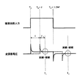
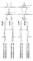
ひとつの解決策として、図4及び図5に示すように、光変調器へのバイアス印加用に追加の電源電圧VDDP、VDDNを用いて、ドライバの電源電圧VDDを1.0V以下の低い電圧に抑えることが考えられる。 As one solution, as shown in FIGS. 4 and 5, the driver's power supply voltage VDD is 1.0 V or less using additional power supply voltages V DDP , V DDN for biasing the light modulator. It is conceivable to suppress it to a low voltage.
図4は、光変調器にVDDよりも高い正のDCバイアス(VDDP)を印加する構成例を示す。図5は、光変調器にCMOSドライバのグランド電位よりも低いバイアス(VDDN)を印加する構成例を示す。図4及び図5でVDD=0.9V、VSS=0Vとすると、光変調器を動作させるためには、VDDP=3.6Vという高電圧(図4)、または、VDDN=−2.7Vという負電圧(図5)が必要になる。光モジュールに供給される一般的な電圧は3.3Vであり、この供給電圧から高電圧または負電圧を生成するために回路が複雑化、大型化する。 FIG. 4 shows a configuration example in which a positive DC bias ( VDDP ) higher than VDD is applied to the light modulator. FIG. 5 shows a configuration example in which a bias (VDDN ) lower than the ground potential of the CMOS driver is applied to the light modulator. V DD = 0.9V in FIGS. 4 and 5, when V SS = 0V, to operate the optical modulator, a high voltage of V DDP = 3.6V (FIG. 4), or, V DDN = - A negative voltage of 2.7V (Fig. 5) is required. The general voltage supplied to the optical module is 3.3V, and the circuit becomes complicated and large in order to generate a high voltage or a negative voltage from this supply voltage.
さらに別の問題として、イコライズ回路はCMRM=CFRFが成り立つことを前提としているが、光変調器やレーザダイオードの接合容量CMと接合抵抗RMは電圧に対して非線形であり、入力データ「1」、「0」に応じて切り替えられるドライバ出力の変化により、必ずしもCMRM=CFRFが成り立たなくなる。そのため、フィルタ(イコライズ回路)の特性を駆動対象である光回路素子(光変調器、レーザダイオード等を含む)の特性に合わせる構成が望まれる。 As still another problem, although equalizing circuit assumes that holds the C M R M = C F R F, the junction resistance R M and the junction capacitance C M of the optical modulator and a laser diode is nonlinear with respect to the voltage Yes, due to the change in the driver output that can be switched according to the input data "1" and "0", C M R M = C F R F does not always hold. Therefore, it is desired to have a configuration in which the characteristics of the filter (equalize circuit) are matched with the characteristics of the optical circuit element (including the optical modulator, laser diode, etc.) to be driven.
上記の課題に鑑みて、実施形態では、駆動回路と光回路素子の間に、キャパシタと電流源を有する周波数特性調整回路を配置し、駆動回路の出力電圧に応じて電流源から光回路素子に供給される電流量を調整する。これにより、低い駆動電圧で光回路素子を高速駆動し、良好な応答特性の光出力を実現する。 In view of the above problems, in the embodiment, a frequency characteristic adjustment circuit having a capacitor and a current source is arranged between the drive circuit and the optical circuit element, and the current source is changed to the optical circuit element according to the output voltage of the drive circuit. Adjust the amount of current supplied. As a result, the optical circuit element is driven at high speed with a low drive voltage, and an optical output with good response characteristics is realized.
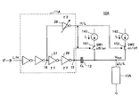
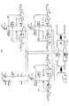
図6は、実施形態の周波数特性調整回路10の基本構成と、これを用いた光送信フロントエンドの構成を示す図である。図3に示されたRFとCFからなるイコライズ回路の代わりに、周波数特性調整回路10が、駆動回路11と光変調器13の間に配置される。なお光変調器13は光回路素子の一例であり、VCSEL(Vertical Cavity Surface Emitting Laser)等の面発光レーザを用いてもよい。駆動回路11は、たとえばCMOSドライバであり、入力データに応じてVDD(H)またはVSS(L)を出力する。周波数特性調整回路10は容量CFのキャパシタ12と、電流供給回路14を含む。容量CFは図3のイコライズ回路と同じである。違いはRFの代わりに、電流供給回路14の第1の電流源141と、第2の電流源142を用いて、駆動回路11の出力に応じて電流I1または電流I2を供給する。たとえば、PMOS111がONしているときに電流I2を出力し、NMOS112がONしているときに電流I1を出力する。
FIG. 6 is a diagram showing a basic configuration of the frequency
図4(A)の構成でPMOSがONしているときの電流をI2、NMOSがONしているときの電流をI1とすると、図6の回路は図4(A)の回路と同じ動作が可能であり、かつ電圧VDDHはVDDPよりも低い。また、図5のような負電源も不要である。図4の回路と同じ動作が、より低い電圧と簡単な回路構成で実現できる。 Assuming that the current when the MOSFET is ON is I 2 and the current when the MOSFET is ON is I 1 in the configuration of FIG. 4 (A), the circuit of FIG. 6 is the same as the circuit of FIG. 4 (A). It is operational and the voltage V DDH is lower than V DDP. Further, the negative power supply as shown in FIG. 5 is not required. The same operation as the circuit of FIG. 4 can be realized with a lower voltage and a simple circuit configuration.
図7は、図6の等価回路である。入力データに応じて駆動回路11のスイッチSW1とSW2が切り替えられ、周波数特性調整回路10に電流I1または電流I2が流れる。ノードVoutから光変調器の等価回路13eqに、電流Imが流れる。等価回路13eqにおいて、ノードVoutと光変調器の接地電位VSSの間の電位差Vmが、光変調器13にかかる電圧である。電流源141及び142から供給される電流I1とI2の値は、駆動回路11の出力が高速に切り替わっても光変調器13で安定した応答特性が得られるように、所定の条件を満たすように設定されている。
FIG. 7 is an equivalent circuit of FIG. The switches SW1 and SW2 of the
図8と図9を参照して、電流供給回路14で用いられる電流値の設定を説明する。図8は、従来構成のイコライズ回路を用いたときの周波数特性を示す。横軸は周波数、縦軸はログスケールによるゲイン(光変調器にかかる電圧)である。イコライズ回路を挿入してη=0.1に設定することで、高周波側に帯域が拡張されている。
The setting of the current value used in the
図8の実線は、式(2)でCFRF=CMRMが成り立つことを条件、すなわち式(3)で表される小信号特性をプロットしたものである。帯域が拡張されてもフラットな特性が維持されている。しかし、プロセスばらつきにより、CF、RF、CM、RMが設計値からずれたり、接合容量や接合抵抗の電圧依存性に強い非線形な要素が含まれると、必ずしもCFRF=CMRMは成り立たなくなる。 The solid line in FIG. 8 is a plot C F R F = C M R M condition that is satisfied by the equation (2), i.e., the small signal characteristics of the formula (3). Flat characteristics are maintained even when the band is expanded. However, process variations, C F, R F, C M, R M is or shifted from the design value, is contained strong nonlinear element voltage dependence of the junction capacitance and junction resistance, always C F R F = C M R M will not hold.
そこで、CFRF>CmRmCFRFの条件での周波数特性(細かい破線)と、CFRF<CMRMの条件での周波数特性(粗い破線)を合わせて示す。CFRF=CMRMが満たされない場合、特に、容量CFまたはCMを変えたときに、100MHz〜数GHzの中周波数領域Mで周波数特性がフラットでなくなる。 Therefore, C F R F> C m R m C F frequency characteristics in terms of R F and (short dashed line) shows the combined C F R F <frequency characteristic of the condition of C M R M (long dashed line) .. If C F R F = C M R M is not satisfied, in particular, when changing the capacitance C F or C M, the frequency characteristics in the frequency region M in the 100MHz~ several GHz is no longer flat.
したがって、光変調器の電流-電圧特性、または容量-電圧特性が非線形であるということは、電流または容量値の電圧依存性が変化することを意味する。この場合、図8のように中周波数帯域での特性変動が生じる。特に、順方向のPN接合では電圧に対する接合容量の変化が非線形であり、周波数特性が変動しやすい。 Therefore, a non-linear current-voltage characteristic or capacitance-voltage characteristic of an optical modulator means that the voltage dependence of the current or capacitance value changes. In this case, characteristic fluctuation occurs in the middle frequency band as shown in FIG. In particular, in a forward PN junction, the change in junction capacitance with respect to voltage is non-linear, and the frequency characteristics tend to fluctuate.
中周波数領域で周波数特性が変動する理由のひとつは、図1(B)で入力データに応じてCMOSドライバの出力レベル(「H」または「L」)が変わると、ノードVoutに存在する電荷量が変わり、信号の変化が、その電荷量の変化の時定数(〜CMRM)より早いか遅いかでゲインが変化するためである。中周波数領域Mで特性が変動すると、データ依存性のジッタである符号間干渉(ISI:Inter-Symbol Interference)が生じる。したがって、図7において、駆動回路11の出力レベルに応じて、周波数特性調整回路10から供給される電流量I1、I2を変調器の特性やCFのプロセスばらつきに対して、適切な値に設定できることが望まれる。
One of the reasons why the frequency characteristics fluctuate in the medium frequency region is the amount of charge existing in the node Vout when the output level (“H” or “L”) of the CMOS driver changes according to the input data in FIG. 1 (B). changes, signal change is early or late or gain than a constant (~C M R M) when the change of the charge amount is to change. When the characteristics fluctuate in the middle frequency region M, inter-symbol interference (ISI), which is a data-dependent jitter, occurs. Therefore, in FIG. 7, the current amounts I 1 and I 2 supplied from the frequency
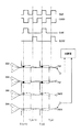
図9は、周波数特性調整回路10の電流設定条件を示す図である。図9の左図は、低電位電圧VSSが選択されて光変調器に電流I1が流れる状態を示す。図9の右図は、高電位電圧VDDが選択されて光変調器13に電流I2が流れる状態を示す。左図でVSSが選択されると、ノード16に電圧VM1が現れる。このとき、スイッチ151がオンして光変調器13に電流IM(VM1)が流れる。右図でVDDが選択されると、ノード16に電圧VM2が現れる。このとき、スイッチ152がオンしてノード17から光変調器13に電流IM(VM2)が流れる。
FIG. 9 is a diagram showing current setting conditions of the frequency
周波数特性調整回路10のキャパシタ12の容量をCF、光変調器13の電流-電圧特性をIM(VM)、光変調器13の電荷-電圧特性をQM(VM)とする。周波数特性をフラットにするための電流条件は、
IM(VM1)=I1 (4)
IM(VM2)=I2 (5)
Q1−CF(Vss-VM1)=Q2−CF(VDD-VM2) (6)
である。ここで、Q1は、光変調器13に電圧VM1がかかるときの容量CMの電荷量である(Q1=QM(VM1))。Q2は、光変調器13に電圧VM2がかかるときの容量CMの電荷量である(Q2=QM(VM2))。CF(Vss-VM1)は駆動回路11で電圧Vssが選択されたときのキャパシタ12の電荷量、CF(VDD-VM1)は駆動回路11で電圧VDDが選択されたときのキャパシタ12の電荷量である。
Capacity C F capacitor 12 of the frequency
I M (V M1) = I 1 (4)
I M (V M2) = I 2 (5)
Q1-C F (V ss -V M1) = Q2-C F (V DD -V M2) (6)
Is. Here, Q1 is a voltage V M1 to the
この電流条件は、入力データ「0」、「1」の変化にかかわらずノード16での電荷量を一定に保つことを意味する。これにより、帯域拡張された光変調器13で周波数特性がフラットになり、データ依存性のジッタを生じさせずに高速動作が実現できる。
This current condition means that the amount of charge at the
電流源141、142を付加することにより消費電流の増加はあるが、駆動回路11の電源電圧自体を低く抑えることができるため、あるいは、バイアス印加用に追加の電源電圧を必要としないため、全体の消費電力やコストを抑えることができる。
Although the current consumption is increased by adding the
図10は、実施例1の周波数特性調整回路10Aを用いたレーザダイオード13Aの調整動作を示す。レーザダイオードは、たとえばVCSEL等の面発光レーザである。駆動回路11AにデータLが入力されると、ノード18が「L」となる。ノード18で駆動信号が分割され、一方の信号は遅延回路27、28によりτ1+τ2の遅延を受け、ノード19で「L」になる。この場合、キャパシタ12に「L」が出力されるとともに、SW1がOFFとなり電流I1は流れない。分割された他方の信号は、遅延回路29で遅延調整されて「H」が出力される。遅延回路29の遅延量τ3は、τ3=τ1+τ2となるように調整されている。電流I1の遮断と同じタイミングで、遅延回路29の出力「H」によりスイッチSW2がONして、レーザダイオード13Aに電流I2が流れる。
FIG. 10 shows an adjustment operation of the
駆動回路11AにデータHが入力されると、中間ノード18が「H」となる。中間ノード18で駆動信号が分割され、一方の信号は遅延回路27、28によりτ1+τ2の遅延を受け、出力ノード19で「H」になる。この場合、キャパシタ12に「H」が出力されるとともに、周波数特性調整回路10AのスイッチSW1がONになり、レーザダイオード13Aに電流I1が流れる。分割された他方の信号は、遅延回路29でτ3の遅延を受けて駆動回路11Aから「L」が出力される。電流I1が流れるのと同じタイミングで、遅延回路29の出力「L」により周波数特性調整回路10AのスイッチSW2がOFFとなり、電流I2が遮断される。
When the data H is input to the
この構成により、ノードVoutでの電荷量は常に一定となり、レーザダイオード13Aが高速駆動信号で駆動される場合でも入力データに応じた応答特性を良好に保つことができる。
With this configuration, the amount of charge at the node Vout is always constant, and even when the
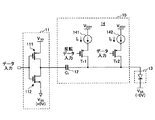
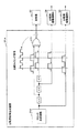
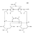
図11は、実施例2の周波数特性調整回路10Bを用いた光変調器13Bの調整動作を示す。実施例2では、マッハツェンダ型光変調器13Bを駆動する。この例では、インバータ31、32、33、34を含む差動構成の駆動回路が用いられている。
FIG. 11 shows an adjustment operation of the
光源であるレーザダイオード(LD)40から出力された光を2つに分岐して、分岐した光を光導波路131と132に入力する。電極133、134への電圧印加により、光導波路131と132の実効光路長に変化が与えられた後、合波器136で合波される。合波器136において光導波路131を伝搬した光と光導波路132を伝搬した光に位相差がないときは、最大の出力が得られる。2つの光の間に波長の半分の光路長差が生じているときは、打ち消し合って出力が小さくなる。これにより強度変調が行われる。
The light output from the laser diode (LD) 40, which is a light source, is branched into two, and the branched light is input to the
インバータ31にデータ「H」が入力されるとインバータ32を経てキャパシタ12−1に「H」電圧が出力される。このとき、インバータ31から「L」電圧が出力されてスイッチSW3とSW6をOFFにする。他方、インバータ33に反転データ「L」が入力されてインバータ34からキャパシタ12−2に「L」電圧が出力される。インバータ33から出力される「H」電圧は、スイッチSW4とSW5をONにする。
When the data "H" is input to the
スイッチSW3とSW5はノード35に接続され、スイッチSW4とSW6はノード36に接続されている。入力データ「H」と反転データ「L」によりノード35にデータの変化に伴うAC電流と電流I2の合成電流が流れて、マッハツェンダ型光変調器13Bの一方の光導波路131の電極133に、データの変化に伴うAC電流と電流I2の合成電流が流れる。同時に、ノード36にデータの変化に伴うAC電流と電流I1の合成電流が流れ、光導波路132の電極134にデータの変化に伴うAC電流と電流I1の合成電流が流れる。光導波路132を伝搬する光は屈折率変化に応じた位相調整を受けた後に、位相シフタ135でπ/2の位相シフトを受けて、光導波路131を伝搬する光と合波される。このとき、変調器出力は最大になる。
The switches SW3 and SW5 are connected to the
インバータ31にデータ「L」が入力され、インバータ33に反転データ「H」が入力されるときは、上記と逆の動作になり、電極133に電流I1が流れ、電極134に電流I2が流れる。光導波路132を伝搬する光は屈折率変化に応じた位相調整を受けた後に位相シフタ135でπ/2の位相シフトを受けて、光導波路131を伝搬する光と合波される。合波された光は打ち消し合って変調器出力は最小となる。
When the data "L" is input to the
図12は、実施例2の周波数特性調整回路10Bをトランジスタ回路で表記した図である。第1の電流源141は電流I1を生成し、第2の電流源142は電流I2を生成する。電流源141は、Tr17を介してTr18のゲートに接続されており、電流源142はTr23を介してTr24のゲートに接続されている。
FIG. 12 is a diagram showing the frequency
インバータ31にデータ「H」が入力されるとインバータ32を経てキャパシタ12−1に「H」電圧が出力される。インバータ31からの出力電圧「L」はPMOSTr13とPMOSTr22をONにし、NMOSTr16とNMOSTr19をOFFにする。他方、インバータ33に反転データ「L」が入力されてインバータ34からキャパシタ12−2に「L」電圧が出力される。インバータ33からの出力電圧「H」は、NMOSTr14とNMOSTr21をONにし、PMOSTr15とPMOSTr20をOFFにする。NNOSTr14、NMOSTr16、MOSTr19とMOSTr21は必須ではなく、用いなくてもよい。
When the data "H" is input to the
Tr13とTr14のONにより、ノード42は電流I1が流れ、同時にTr15とTr16のOFFにより、ノード41への電流の供給は遮断される。また、Tr21とTr22のONによりノード41に電流I2が流れ、同時に、Tr19とTr20のOFFによりノード42への電流の供給は遮断される。したがって、ノード35にはCFで低周波成分がカットされたデータの変化に伴う電流とノード41に現れる電流I2だけが流れ、ノード36には、CFで低周波成分がカットされたデータの変化に伴う電流とノード42に現れる電流I1だけが流れる。この結果、光導波路132の電極134にCFで低周波成分がカットされた、データの変化に伴う電流と電流I1が流れる。光導波路131の電極133にはCFで低周波成分がカットされたデータの変化に伴う電流とI2が流れる。合波器136で合波された光は強め合って変調器出力は最大となる。
When Tr 13 and Tr 14 are turned on, the
インバータ31にデータ「L」が入力され、インバータ33に反転データ「H」が入力されるときは、上記と逆の動作になり、電極133に電流I1が流れ、電極134に電流I2が流れる。合波器136で合波された光は打ち消し合って変調器出力は最小となる。
When the data "L" is input to the
図11と図12で、マッハツェンダ型光変調器13Bの光導波路131と132はPN接合で形成されている。接合容量が大きくかつ容量-電圧特性が非線形なPN接合を有する光変調器13Bを用いる場合でも、周波数特性調整回路10Bを用いることで、低電圧の高速駆動の際に良好な応答特性が得られる。
In FIGS. 11 and 12, the
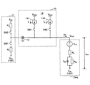
図13は、実施例3の周波数特性調整回路10Cを用いた光変調器13Bの調整動作を示す。実施例3では、マッハツェンダ型光変調器13Bを駆動する。この例では、電流源として、第1の電流I1を供給する第1の電流源147,148と、差分電流(I2−I1)を供給する第2の電流源149を用いる。また、インバータ31、32、33、34を含む差動構成の駆動回路が用いられている。
FIG. 13 shows an adjustment operation of the
光源であるレーザダイオード(LD)40から出力された光を2つに分岐して、分岐した光を光導波路131と132に入力する。電極133、134への電圧印加により、光導波路131と132の実効光路長に変化が与えられた後、合波器136で合波される。合波器136において光導波路131を伝搬した光と光導波路132を伝搬した光に位相差がないときは、最大の出力が得られる。2つの光の間に波長の半分の光路長差が生じているときは、打ち消し合って出力が小さくなる。これにより強度変調が行われる。
The light output from the laser diode (LD) 40, which is a light source, is branched into two, and the branched light is input to the
インバータ31にデータ「H」が入力されるとインバータ32を経てキャパシタ12−1に「H」電圧が出力される。このとき、インバータ31から「L」電圧が出力されてスイッチSW7をOFFにする。他方、インバータ33に反転データ「L」が入力されてインバータ34からキャパシタ12−2に「L」電圧が出力される。インバータ33から出力される「H」電圧は、スイッチSW9をONにする。SW8とSW10は常時ONである。周波数特性調整回路10Cの特性に問題がない場合は、SW8とSW10を省略してもよい。
When the data "H" is input to the
スイッチSW7とSW8はノード46に接続され、スイッチSW9とSW10はノード45に接続されている。入力データ「H」と反転データ「L」によりノード45にはCFで低周波成分がカットされたデータの変化に伴う電流と電流I2−I1とI1との合成電流I2が流れて、マッハツェンダ型光変調器13Bの一方の光導波路131の電極133に電流I2が流れる。同時に、ノード46にはCFで低周波成分がカットされたデータの変化に伴う電流と電流I1が流れ、光導波路132の電極134に電流I1が流れる。光導波路132を伝搬する光は屈折率変化に応じた位相調整を受けた後に、位相シフタ135でπ/2の位相シフトを受けて、光導波路131を伝搬する光と合波される。このとき、変調器出力は最大になる。
The switches SW7 and SW8 are connected to the
インバータ31にデータ「L」が入力され、インバータ33に反転データ「H」が入力されるときは、上記と逆の動作になり、電極133に電流I1が流れ、電極134に電流I2が流れる。光導波路132を伝搬する光は屈折率変化に応じた位相調整を受けた後に位相シフタ135でπ/2の位相シフトを受けて、光導波路131を伝搬する光と合波される。合波された光は打ち消し合って変調器出力は最小となる。
When the data "L" is input to the
図14は、図13(実施例3)の周波数特性調整回路10Cを、トランジスタ回路で表記した図である。第1の電流源241は電流I1を生成し、第2の電流源149は電流(I2−I1)を生成する。この差分電流をΔIと称してもよい。電流源241は、Tr7を介してTr8とTr9のゲートに接続されており、TrがONする条件ではノード43とノード44に電流I1が現れる。電流源149は、Tr10を介してTr11のゲートに接続されている。
FIG. 14 is a diagram showing the frequency
インバータ31にデータ「H」が入力されるとインバータ32を経てキャパシタ12−1に「H」電圧が出力される。インバータ31からの出力電圧「L」はPMOSTr6をONにし、NMOSTr3をOFFにする。他方、インバータ33に反転データ「L」が入力されてインバータ34からキャパシタ12−2に「L」電圧が出力される。インバータ33からの出力電圧「H」は、NMOSTr5をONにし、PMOSTr4をOFFにする。NNOSTr3とNMOSTr5は必須ではなく、用いなくてもよい。
When the data "H" is input to the
Tr6のONによりノード49に差分電流ΔIが流れ、ノード47に現れる電流I1と足し合わされ、ノード43にはΔI+I1=I2が流れる。この結果、ノード45にはCFで低周波成分がカットされたデータの変化に伴う電流と電流I2が流れ、光導波路131の電極133にデータの変化に伴うAC電流と電流I2が流れる。同時に、Tr4のOFFによりノード50への電流の供給は遮断される。ノード46には、CFで低周波成分がカットされたデータの変化に伴う電流とノード48に現れる電流I1だけが流れる。この結果、光導波路132の電極134にCFで低周波成分がカットされたデータの変化に伴う電流と電流I1が流れる。合波器136で合波された光は強め合って光変調器13Bの出力は最大となる。
Differential current [Delta] flows in the
インバータ31にデータ「L」が入力され、インバータ33に反転データ「H」が入力されるときは、上記と逆の動作になり、電極133にCFで低周波成分がカットされたデータの変化に伴う電流と電流I1が流れ、電極134にCFで低周波成分がカットされたデータの変化に伴う電流と電流I2が流れる。合波器136で合波された光は打ち消し合って変調器出力は最小となる。
When the data "L" is input to the
図13と図14で、マッハツェンダ型光変調器13Bの光導波路131と132はPN接合で形成されている。接合容量が大きくかつ容量-電圧特性が非線形なPN接合を有する光変調器13Bを用いる場合でも、周波数特性調整回路10Cを用いることで、低電圧の高速駆動の際に良好な応答特性が得られる。
In FIGS. 13 and 14, the
図15は、実施例4の周波数特性調整回路10Dを用いた光変調器13Cの調整動作を示す。実施例4では、マッハツェンダ型光変調器13Cを用いて2ビットのパルス振幅変調(PAM-4)を行う。マッハツェンダ型光変調器13Cの光導波路131と132のそれぞれに、最下位ビット(LSB)用の電極137、139と、最上位ビット(MSB)用の電極138、140が配置されている。位相シフタ135で、2つの光導波路131、132を伝搬する光の間にπ/2の位相差が与えられるのは実施例2と同様である。
FIG. 15 shows an adjustment operation of the light modulator 13C using the frequency
周波数特性調整回路10DはLSB用の回路部分10D−1と、MSB用の回路部分10D−2を含む。回路部分10D−1と10D−2の基本構成と動作は、図11の構成及び動作と同じであり、重複する説明を省略する。
The frequency
LSB用の回路部分10D−1は、電流源143と144を有する。MSB用の回路部分10D−2は、電流源145と146を有する。電流源143は電流IL2を生成し、電流源144は電流IL1を生成する。電流源145は電流IM2を生成し、電流源146は電流IM1を生成する。電流IL1と電流IM1の比は通常は1:2であるが、違う値でもかまわない。電流源143、144、145、146は同じ電源電圧VDDHに接続されていてもよい。2ビットの入力データの値に対して、変調1、変調2で生成された位相変化の和の位相変化として、変調器光変調器13Cで4種類の位相変化が生成される。
The
たとえば、LSB用の回路部分10D−1への入力データが「H」の場合、電極137にCFL(12L−1)で低周波成分がカットされたデータの変化に伴う電流と電流IL2が流れ、電極139にCFL(12L−2)で低周波成分がカットされたデータの変化に伴う電流と電流IL1が流れる。MSB用の回路部分10C−2への入力データが「H」の場合、電極138にCFM(12M−1)で低周波成分がカットされたデータの変化に伴う電流と電流IM2が流れ、電極140にCFM(12M−2)で低周波成分がカットされたデータの変化に伴う電流と電流IM1が流れる。合波器136では、回路部分10C−1と10C−2に印加される電圧に応じて4つの振幅のいずれかを有するパルス波形が生成される。
For example, if the input data to the
図16は、実施例5の周波数特性調整回路10Eを用いて、マッハツェンダ型光変調器13Dの駆動動作を調整する。図15では、マッハツェンダ型光変調器13CでLSBとMSBに別々の電極を配置していたが、図16では、光導波路131に配置される電極161と、光導波路132に配置される電極162を用いる。
FIG. 16 uses the frequency
実施例1〜4と同様に、LSB用の回路部分では、入力される電圧信号レベル(HまたはL)に応じて、異なる電流値IL2またはIL1が流れる(図中では「IL2/IL1」、「IL1/IL2」と表記)。MSB用の回路部分では、入力される電圧信号レベル(HまたはL)に応じて、異なる電流値IM2またはIM1が流れる(図中では「IM2/IM1」、「IM1/IM2」と表記)。 Similar to Examples 1 to 4, different current values IL2 or IL1 flow in the circuit portion for the LSB depending on the input voltage signal level (H or L) (“IL2 / I” in the figure). Notated as "L1" and " IL1 / IL2 "). The circuit portion for MSB, in accordance with the voltage level of the signal input (H or L), different current value I M2 or I M1 flows (in the figure "I M2 / I M1", "I M1 / I M2 Notation).
ここで、NRZ(Non-Return to Zero)信号に対して図9を参照して述べた周波数特性をフラットにするための電流条件と同様に、図16の構成でPAM4信号に対する周波数特性をフラットにするための条件を考える。図16での条件は下記で表される。 Here, similar to the current conditions for flattening the frequency characteristics described with reference to FIG. 9 for the NRZ (Non-Return to Zero) signal, the frequency characteristics for the PAM4 signal are flattened with the configuration of FIG. Consider the conditions for doing so. The conditions in FIG. 16 are represented below.
IM(VM00)=IM1+IL1 (7)
IM(VM01)=IM1+IL2 (8)
IM(VM10)=IM2+IL1 (9)
IM(VM11)=IM2+IL2 (10)
Q00−CFL(VSS-VM00)−CFM(VSS-VM00)
≒Q00−CFL(VDD-VM01)−CFM(VSS-VM01)
≒Q00−CFL(VSS-VM10)−CFM(VDD-VM10)
≒Q00−CFL(VDD-VM11)−CFM(VDD-VM11) (11)
ここで変調器の電流-電圧特性をIM(VM)は、マッハツェンダ型光変調器13Dの電流−電圧特性である。
I M (V M00) = I M1 + I L1 (7)
I M (V M01) = I M1 + I L2 (8)
I M (V M10) = I M2 + I L1 (9)
I M (V M11) = I M2 + I L2 (10)
Q 00 -C FL (V SS -V M00) -C FM (V SS -V M00)
≒ Q 00 -C FL (V DD -V M01) -C FM (V SS -V M01)
≒ Q 00 -C FL (V SS -V M10) -C FM (V DD -V M10)
≒ Q 00 -C FL (V DD -V M11) -C FM (V DD -V M11) (11)
Wherein the modulator of the current - voltage characteristics I M (V M), the current of the Mach-Zehnder
図16の構成を用いた場合も、低い駆動電圧で光変調器13Dが高速駆動されるときに良好な応答特性で歪の少ないパルス形状を得ることができる。変調器13Dの電気特性に非線形が強くなると等式は成り立たなく場合もあり得るが、その場合でも近似され得る。
Even when the configuration of FIG. 16 is used, it is possible to obtain a pulse shape with good response characteristics and less distortion when the
図17は、実施例6として、周波数特性調整回路10Fを用いて、マッハツェンダ型光変調器13Fの駆動動作を調整する。図15では、マッハツェンダ型光変調器13CでLSBとMSBに別々の電極を配置していたが、図17では、実施例5と同様に、光導波路131に配置される電極161と、光導波路132に配置される電極162を用いる。また、電流源250、251、252、253、254を用いる。
In FIG. 17, as the sixth embodiment, the drive operation of the Machzenda type
電流源250と電流源251は、電流I00を供給する。電流源250に接続されるスイッチSW19と、電流源251に接続されるスイッチSW20は、常時オンである。周波数特性調整回路10Fの特性によっては、SW19とSW20を省略してもよい。
The
データ信号C1とその反転信号が入力される駆動回路(インバータ81〜84を含む)に対応する回路部分では、キャパシタンスCF1のキャパシタ114−1,114−2が用いられる。入力される電圧信号の値(HまたはL)に応じて、ノード67,68を流れる電流値は、I01−I00か、またはゼロになる。
Capacitors 114-1 and 114-2 of capacitance C F1 are used in the circuit portion corresponding to the drive circuit (including the
データ信号C2とその反転信号が入力される駆動回路(インバータ85〜88を含む)に対応する回路部分では、キャパシタンスCF2のキャパシタ115−1,115−2が用いられる。入力される電圧信号の値に応じて、ノード69,70を流れる電流値は、I10−I01か、またはゼロになる。
Capacitors 115-1 and 115-2 of capacitance C F2 are used in the circuit portion corresponding to the drive circuit (including the
データ信号C3とその反転信号が入力される駆動回路(インバータ89〜92を含む)に対応する回路部分では、キャパシタンスCF3のキャパシタ116−1,116−2が用いられる。入力される電圧信号の値に応じて、ノード71,72を流れる電流値は、I11−I10か、またはゼロになる。
Capacitors 116-1 and 116-2 of capacitance C F3 are used in the circuit portion corresponding to the drive circuit (including the
図17の実施例6で4つの電圧レベルVM00、VM01、VM10、VM11を用いて変調するときに周波数特性をフラットにするための条件は、
IM(VM00)=I00 (12)
IM(VM01)=I00+(I01−I00)=I01 (13)
IM(VM10)=I00+(I01−I00)+(I10−I01)=I10 (14)
IM(VM11)=I00+(I01−I00)+(I10−I01)+(I11−I10)=I11
(15)
Q00−CF1(VSS−VM00)−CF2(VSS−VM00)−CF3(VSS−VM00)
=Q01−CF1(VDD−VM01)−CF2(VSS−VM01)−CF3(VSS−VM01)
=Q10−CF1(VDD−VM10)−CF2(VDD−VM10)−CF3(VSS−VM10)
=Q11−CF1(VDD−VM11)−CF12(VDD−VM11)−CF3(VDD−VM11)
(16)
である。
Conditions for the frequency characteristic flat when modulated with Example 6 in four voltage levels V M00, V M01, V M10 , V M11 of FIG. 17,
I M (V M00) = I 00 (12)
I M (V M01) = I 00 + (I 01 -I 00) = I 01 (13)
I M (V M10) = I 00 + (I 01 -I 00) + (I 10 -I 01) = I 10 (14)
I M (V M11) = I 00 + (I 01 -I 00) + (I 10 -I 01) + (I 11 -I 10) =
(15)
Q 00- C F1 (V SS- V M00 ) -C F2 (V SS- V M00 ) -C F3 (V SS- V M00 )
= Q 01- C F1 ( VDD- V M01 ) -C F2 (V SS- V M01 ) -C F3 (V SS- V M01 )
= Q 10 -C F1 (V DD -V M10) -C F2 (V DD -V M10) -C F3 (V SS -V M10)
= Q 11- C F1 ( VDD- V M11 ) -C F12 ( VDD- V M11 ) -C F3 ( VDD- V M11 )
(16)
Is.
図17の構成を用いた場合も、低い駆動電圧で光変調器13Fが高速駆動されるときに良好な応答特性で歪の少ないパルス形状を得ることができる。
Even when the configuration of FIG. 17 is used, it is possible to obtain a pulse shape with good response characteristics and less distortion when the
実施例1〜6の周波数特性調整回路は、駆動回路から受け取る電圧に応じて異なる電流値の電流を駆動対象である光回路素子に供給することで、低い電圧で光回路素子を高速駆動して良好な応答特性を実現した。実施例1〜6の回路は、以下で述べる構成によりさらに改善することが可能である。 The frequency characteristic adjustment circuit of Examples 1 to 6 drives the optical circuit element at high speed with a low voltage by supplying a current having a different current value depending on the voltage received from the drive circuit to the optical circuit element to be driven. Achieved good response characteristics. The circuits of Examples 1 to 6 can be further improved by the configuration described below.
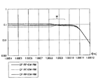
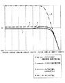
図18は、周波数特性調整回路のさらなる改善を説明する図である。イコライズ回路を用いない状態(一点鎖線Wで示される周波数特性)から、実線Yのように設計されたイコライズ回路を挿入することで帯域を10倍伸ばす(DCゲインは10分の1)ことができる。ただし、プロセスばらつきなどにより容量が設計値からたとえば20%ダウンした場合、点線Zで示すように、中周波数帯域で周波数特性がフラットでなくなり、信号にシンボル間干渉(ISI)が生じる。 FIG. 18 is a diagram illustrating further improvement of the frequency characteristic adjustment circuit. The band can be extended 10 times (DC gain is 1/10) by inserting an equalize circuit designed as shown by the solid line Y from the state where the equalize circuit is not used (frequency characteristics indicated by the alternate long and short dash line W). .. However, when the capacitance is reduced by, for example, 20% from the design value due to process variation or the like, the frequency characteristics are not flat in the middle frequency band as shown by the dotted line Z, and intersymbol interference (ISI) occurs in the signal.
これを解決するために、実施例1〜6では光回路素子に供給される電流の設定を変更して、破線Xのようにフラットな周波数特性を実現した。周波数特性はフラットであるが、DCゲインや帯域が設計した値からわずかにずれてしまうことがある。 In order to solve this, in Examples 1 to 6, the setting of the current supplied to the optical circuit element was changed to realize a flat frequency characteristic as shown by the broken line X. The frequency response is flat, but the DC gain and band may deviate slightly from the designed values.
設計値からのずれを解消するために、バラクタのような可変容量を用いるという方法も考えられるが、寄生抵抗分が大きく、また線形性(容量−電圧特性)も良くないので、周波数特性を悪化させるおそれがある。 In order to eliminate the deviation from the design value, it is possible to use a variable capacitance such as a varicap, but the parasitic resistance is large and the linearity (capacity-voltage characteristic) is not good, so the frequency characteristic deteriorates. There is a risk of causing it.
そこで、実施例7では、駆動回路とキャパシタの組を複数配置し、一部またはすべての組で駆動回路の出力状態を「アクティブ」と「High-Z」(高インピーダンス)の間で選択可能にする。 Therefore, in the seventh embodiment, a plurality of sets of the drive circuit and the capacitor are arranged, and the output state of the drive circuit can be selected between "active" and "High-Z" (high impedance) in some or all sets. do.
図19は、実施例7の周波数特性調整回路10Gを用いた光変調器13Bの動作例を示す。この例では、図13(実施例3)と同様に、第1の電流I1を供給する第1の電流源147,148と、差分電流(I2−I1)を供給する第2の電流源149を用いて、マッハツェンダ型光変調器13Bを駆動する。
FIG. 19 shows an operation example of the
データ信号の入力側で、図13のインバータ31、32及びキャパシタ(CF)12−1に替えて、駆動回路としての出力状態可変バッファ201とキャパシタCF−1の組を複数配置する。反転データ信号の入力側で、図13のインバータ33、34及びキャパシタ(CF)12−2に替えて、駆動回路としての出力状態可変バッファ203とキャパシタCF−2の組を複数配置する。
On the data signal input side, instead of the
より具体的には、インバータ31、32、及びその出力に接続されているCFが、出力状態可変バッファ201−1とCF1、出力状態可変バッファ201−2とCF2、…、出力状態可変バッファ201−mとCFmに分割されている。同様に、インバータ33、34、及びその出力に接続しているCFが、出力状態可変バッファ203−1とCF1、出力状態可変バッファ203−2とCF2、…、出力状態可変バッファ203−mとCFmに分割されている。
More specifically, the
出力状態可変バッファ201−1〜201−mには、データ信号とともに、制御信号S1,S1、...Smがそれぞれ入力され、出力状態可変バッファ203−1〜203−mには、反転データ信号とともに、制御信号S1,S1、...Smがそれぞれ入力される。 The control signals S1, S1, ... Sm are input to the output state variable buffers 201-1 to 201-m together with the data signals, and the inverted data signals are input to the output state variable buffers 203-1 to 203-m, respectively. At the same time, the control signals S1, S1, ... Sm are input respectively.
出力状態可変バッファ201及び203は、制御信号Sが「High」の場合には入力をバッファして出力するが、制御信号Sが「Low」の場合には出力状態を「High-Z」にする機能を持っている。したがって、キャパシタCF1〜CFmのうち、制御信号Sが「High」の状態の出力状態可変バッファ201または203に接続されているキャパシタだけが周波数特性調整に寄与する。制御信号Sが「Low」である出力状態可変バッファ201または203に接続されているキャパシタは、周波数特性に寄与しない。この構成では、制御信号により信号帯域の調整が可能となり、複数の通信規格に対して対応可能な光送信器が実現できる。
The output state
電流値の切り替えによるマッハツェンダ型光変調器13Bの駆動動作は、実施例3と同じであり、重複する説明を割愛する。なお、電流源につながるスイッチSW7とSW9を制御する信号は、図13では、インバータ31、32の間、およびインバータ33と34の間から取り出しているのに対し、図19では独立してインバータ31、33を設けているが、機能は同じである。
The driving operation of the Machzenda type
図19の構成は、図13の差分電流を用いるスイッチ構成(実施例3)を例にとっているが、図14のトランジスタ構成にも同様に適用される。また、実施例1、2、4〜6のいずれの構成にも適用可能である。いずれの構成と組み合わせた場合にも、制御信号Sによって出力状態可変バッファとキャパシタの所望の組で、出力状態を「アクティブ」または「High-Z」とすることで、周波数特性をフラットにしつつ、設計通りの周波数帯域を実現することができる。 The configuration of FIG. 19 takes as an example a switch configuration (Example 3) using the differential current of FIG. 13, but is similarly applied to the transistor configuration of FIG. Further, it can be applied to any of the configurations of Examples 1, 2, 4 and 6. In any combination, the control signal S sets the output state to "active" or "High-Z" with the desired set of output state variable buffer and capacitor, while flattening the frequency characteristics. The frequency band as designed can be realized.
図20は、出力状態可変バッファ201−mの回路構成例を示す。図20では図示の便宜上、一部の結線が省略されているが、出力状態可変バッファ201にはデータ信号(IN)と、制御信号Smが入力され、インバータ220によって制御信号Smの反転信号が生成される。制御信号Smと反転制御信号Sm(バー)はそれぞれ対応するトランジスタのゲートに接続される。
FIG. 20 shows a circuit configuration example of the output state variable buffer 201-m. Although some connections are omitted in FIG. 20 for convenience of illustration, a data signal (IN) and a control signal Sm are input to the output state
入力211は信号成分212と信号成分213の2系統に分岐され、それぞれインバータ221と224に入力される。インバータ221と224の各々は、電源側がPMOSトランジスタ223、226に接続され、グランド側がNMOSトランジスタ222、225に接続されている。
The
制御信号Smが「High」の時には、NMOSトランジスタ222及び225はONしている。PMOSトランジスタ223及び226も、その入力はインバータ220によって反転され「Low」になっているので、同じくONしている。そのため、インバータ221と224の出力は、入力INと反転した信号となる。また、PMOSトランジスタ228とNMOSトランジスタ230もオフしているため、PMOSトランジスタ227とNMOSトランジスタ229からなる回路はインバータとして働き、結果として出力(OUT)は入力と同じ信号となり、全体としてバッファの役割を果たす。
When the control signal Sm is “High”, the
一方、制御信号Smが「Low」の時には、PMOSトランジスタ223、226と、NMOSトランジスタ222、225はオフし、インバータ221、224は動かず、PMOSトランジスタ228とNMOSトランジスタ230がONとなる。その結果、PMOSトランジスタ227とNMOSトランジスタ229もオフとなり、出力(OUT)は「High-Z」の状態となる。
On the other hand, when the control signal Sm is "Low", the
このように、2段のCMOSインバータを用いて駆動回路、すなわち出力状態可変バッファ201及び203を実現している。2分岐された経路のそれぞれで、初段のCMOSインバータが電源とグランドにスイッチ接続され、第1経路の初段スイッチOFFでCMOSインバータの出力は電源側に固定され、第2経路の初段スイッチOFFでCMOSインバータの出力はグランド側に固定される。このとき、第1経路の初段CMOSインバータの出力が接続される2段目のPMOSと、第2経路の初段CMOSインバータの出力が接続される2段目のNMOSの出力は「High-Z」の状態となる。分割された各駆動回路は図20の出力状態バッファ構成に限定されず、入力値と「High-Z」状態を選択的に出力できる任意の構成をとることができる。
<周波数特性調整回路から供給される電流の制御>
次に、周波数特性調整回路10から供給される電流I1及び電流I2の制御について説明する。電流I1と電流I2の制御は、上述した実施例1〜7のいずれにも適用される。
図21は、周波数特性調整回路10から光回路素子に供給される電流がずれた場合の現象を説明する図である。上段は、中間周波数領域より低い周期で交互に「0」と「1」が切り替わる信号を駆動回路11に入力したときの入力波形、下段は、上段の信号が駆動回路11へ入力されたときに光変調器13に加わる電圧の波形を示す。ここでは、光変調器13は、周波数特性調整回路10から光変調器13に供給される電流が、上述した式(4)と式(5)の条件通り供給されれば設計通りの性能を示すが、
IM(VM1)=I1 (4)
IM(VM2)=I2 (5)
周波数特性調整回路10から光変調器13に供給される電流がI1ではなくI1'になった場合、またはI2ではなくI2'になった場合を考える。図21のパターン(A)は、I1'=I1かつI2'=I2のときの駆動回路入力と光変調器の電圧波形を示す。
In this way, the drive circuit, that is, the output state
<Control of current supplied from frequency characteristic adjustment circuit>
Next, the control of the current I 1 and the current I 2 supplied from the frequency
FIG. 21 is a diagram illustrating a phenomenon when the current supplied from the frequency
I M (V M1) = I 1 (4)
I M (V M2) = I 2 (5)
The current supplied from the frequency
パターン(B)は、I1' <I1、またはI2' >I2のときの波形、パターン(C)は、I1'>I1または、I2' <I2のときの波形である。パターン(A)では、駆動回路への入力信号の変化時(立上りと立下り)に、スパイク状の波形が見られ、その後に一定の電圧が維持される。パターン(B)では、入力値「1」の区間で、スパイクのあとに、あるべき電圧レベルから徐々に上昇している。入力値が「0」に切り替わったときは、逆方向のスパイクが発生し、その後にあるべき電圧レベルに向かって徐々に下降している。 The pattern (B) is the waveform when I 1 '<I 1 or I 2 '> I 2 , and the pattern (C) is the waveform when I 1 '> I 1 or I 2 '<I 2. be. In the pattern (A), a spike-like waveform is seen when the input signal to the drive circuit changes (rising and falling), and then a constant voltage is maintained. In the pattern (B), in the section of the input value "1", after the spike, the voltage level gradually rises from the desired voltage level. When the input value switches to "0", a spike in the opposite direction occurs and then gradually drops towards the voltage level it should be.
パターン(C)では、「0」から「1」への変化によるスパイクの発生後に、電圧レベルが緩やかに下降しているが、所定期間内にあるべき電圧レベルに戻っていない。入力値が「0」になったときは、逆方向のスパイクの後に、あるべき電圧レベルに向かってゆっくりと上昇を続けている。 In pattern (C), the voltage level gradually drops after the spike due to the change from "0" to "1", but does not return to the voltage level that should be within the predetermined period. When the input value reaches "0", it continues to rise slowly toward the desired voltage level after a spike in the opposite direction.
パターン(A)では、スパイクの後に光変調器に加わる電圧が一定のレベルに維持されるのに対し、パターン(B)とパターン(C)では、スパイク(入力値の切り替わり)の後に光変調器に加わる電圧がずれていることがわかる。パターン(B)とパターン(C)で変化の方向は反対である。 In the pattern (A), the voltage applied to the light modulator after the spike is maintained at a constant level, whereas in the pattern (B) and the pattern (C), the light modulator is applied after the spike (switching of the input value). It can be seen that the voltage applied to is deviated. The direction of change is opposite between the pattern (B) and the pattern (C).
図22は、電流設定値のずれを検知する原理を説明する図であり、本来の波形を、時間をずらして重ね合わせものである。実線は図21の波形、破線は時間をずらしたときの波形である。後から変化する破線の波形で、初期のスパイク状の電圧変化が収まったときの時刻T1(入力がHigh)と、時刻T2(入力がLow)で、2つの波形の電圧を比較する。図中のサークルで示すように、パターン(A)では、時間をずらしても実線の波形と破線の波形は時刻T1、T2の双方で同電位となっている。パターン(B)では、時刻T1で実線の電位の方が破線の電位よりも高く(実線>破線)、時刻T2で実線の電位の方が破線の電位よりも低い(実線<破線)。パターン(C)では、時刻T1で実線の電位の方が破線の電位よりも低く(実線<破線)、時刻T2で実線の電位の方が破線の電位よりも高い(実線>破線)。 FIG. 22 is a diagram for explaining the principle of detecting the deviation of the current set value, and is a superimposition of the original waveforms at different times. The solid line is the waveform of FIG. 21, and the broken line is the waveform when the time is staggered. The voltage of the two waveforms is compared at the time T1 (input is High) and the time T2 (input is Low) when the initial spike-shaped voltage change is settled in the waveform of the broken line that changes later. As shown by the circles in the figure, in the pattern (A), the solid line waveform and the broken line waveform have the same potential at both time T1 and T2 even if the time is staggered. In the pattern (B), the potential of the solid line is higher than the potential of the broken line at time T1 (solid line> broken line), and the potential of the solid line is lower than the potential of the broken line at time T2 (solid line <broken line). In the pattern (C), the potential of the solid line is lower than the potential of the broken line at time T1 (solid line <broken line), and the potential of the solid line is higher than the potential of the broken line at time T2 (solid line> broken line).
光変調器に加えられる電圧の元の波形と、時間をずらした波形を比較することで、電流条件がどちらにずれているかを把握することができる。入力信号の周波数をfとし、波形を時間軸上でシフトさせる時間をτとすると、τはできるだけ大きな値が望ましいが、一定の条件が導かれる。 By comparing the original waveform of the voltage applied to the optical modulator with the waveform shifted in time, it is possible to grasp which way the current condition is deviated. Assuming that the frequency of the input signal is f and the time for shifting the waveform on the time axis is τ, τ should be as large as possible, but certain conditions are derived.
図23に示すように、入力が変化したときに光変調器に加得られる電圧に現れるスパイク状の変化が収まるまでにかかる時間をτ1、波形を比較する比較器の反応時間をτ2とすると、
T1>T0+τ+τ1、かつ
T1+τ2<T0+1/(2*f)
という条件が導かれる。この2つの条件式から、
τ<1/(2*f)−τ1−τ2
が導かられる。したがって、波形比較のために、電圧波形をシフトさせる遅延時間τは、τ<1/(2*f)−τ1−τ2を満たすように設定される。
As shown in FIG. 23, it is assumed that the time required for the spike-like change appearing in the voltage applied to the optical modulator when the input changes is settled is τ1, and the reaction time of the comparator comparing the waveforms is τ2.
T1> T0 + τ + τ1 and T1 + τ2 <T0 + 1 / (2 * f)
The condition is derived. From these two conditional expressions
τ <1 / (2 * f) -τ1-τ2
Is guided. Therefore, for waveform comparison, the delay time τ that shifts the voltage waveform is set so as to satisfy τ <1 / (2 * f) −τ1-τ2.
図24A、図24B、及び図24Cは、電圧波形を比較する際に、比較器の入力オフセット電圧を考慮した図である。入力オフセット電圧とは、比較器の誤差を表す値で、出力が0となる時の入力間の電圧差のことである(誤差がないときには0)。図24Aはパターン(A)の条件での電圧波形、図24Bはパターン(B)の条件での電圧波形、図24Cはパターン(C)の条件での電圧波形である。図24A〜図24Cの上から2段目に示すように、入力オフセットがないと仮定すると、スパイクが収束する時刻T1,T2で2つの波形(本来の波形と時間シフトさせた波形)を比較して大小関係を得ることで、電流条件のずれの方向がわかる。図24Aのように、2つの波形で比較した電圧値が同じ場合は、I1'=I1かつI2'=I2であり、周波数特性調整回路10から光回路素子(たとえば光変調器)13に、理論通りの電流が供給されている。図24Bのように、時刻T1で実線(本来の波形)のレベルが破線(シフト波形)のレベルより小さく、時刻T2で実線(本来の波形)のレベルが破線(シフト波形)のレベルよりも大きい場合は、光変調器13に供給される電流がI1'<I1、またはI2'>I2の方向にずれていることがわかる。図24Cのように、時刻T1で実線(本来の波形)のレベルが破線(シフト波形)のレベルより小さく、時刻T2で実線(本来の波形)のレベルが破線(シフト波形)のレベルよりも大きい場合は、光変調器13に供給される電流がI1'>I1、またはI2'<I2の方向にずれている。
24A, 24B, and 24C are diagrams in which the input offset voltage of the comparator is taken into consideration when comparing the voltage waveforms. The input offset voltage is a value representing the error of the comparator, and is the voltage difference between the inputs when the output becomes 0 (0 when there is no error). 24A is a voltage waveform under the condition of the pattern (A), FIG. 24B is a voltage waveform under the condition of the pattern (B), and FIG. 24C is a voltage waveform under the condition of the pattern (C). As shown in the second stage from the top of FIGS. 24A to 24C, assuming that there is no input offset, two waveforms (the original waveform and the time-shifted waveform) are compared at the times T1 and T2 at which the spikes converge. By obtaining the magnitude relationship, the direction of the deviation of the current condition can be known. As shown in FIG. 24A, when the voltage values compared between the two waveforms are the same, I 1 '= I 1 and I 2 '= I 2 and the frequency
しかし、比較器には一般的に入力オフセットが存在する。図24A〜図24Cの下から2段目は、比較器に実線(本来の波形)>破線(シフト波形)と受け取られるオフセットが生じた場合を示す。比較器のオフセットが十分大きいと、電流条件に拠らず、またタイミングにかかわらず、比較器は常に実線(本来の波形)>破線(シフト波形)という判断結果を出力する。逆に、図24A〜図24Cの最下段に示すように、比較器に実線<破線と受け取られるオフセットが生じた場合、そのオフセットが十分大きいと、電流条件に拠らず、またタイミングにかかわらず、比較器は実線<破線という判断結果を出力する。したがって、連続する2回の比較結果が同じで、いずれも実線>破線という判定であれば、2つ目の比較結果が実線<破線となる方向に、比較器のオフセットを調整する。連続する2回の比較結果が同じで、いずれも実線<破線という判定であれば、2つ目の比較結果が実線>破線となる方向に、比較器のオフセットを調整する。これにより、電流条件のずれを正確に判断することができる。 However, the comparator generally has an input offset. The second stage from the bottom of FIGS. 24A to 24C shows the case where the comparator has an offset that is perceived as a solid line (original waveform)> a broken line (shift waveform). If the offset of the comparator is sufficiently large, the comparator always outputs the judgment result of solid line (original waveform)> broken line (shift waveform) regardless of the current condition and timing. On the contrary, as shown in the lowermost part of FIGS. 24A to 24C, when an offset that is perceived as a solid line <dashed line occurs in the comparator, if the offset is sufficiently large, it does not depend on the current condition and regardless of the timing. , The comparator outputs the judgment result that solid line <broken line. Therefore, if the results of two consecutive comparisons are the same and both are determined to be solid line> broken line, the offset of the comparator is adjusted in the direction in which the second comparison result is solid line <broken line. If the results of two consecutive comparisons are the same and both are determined to be solid line <broken line, the offset of the comparator is adjusted in the direction in which the second comparison result is solid line> broken line. This makes it possible to accurately determine the deviation of the current condition.
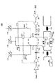
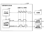
図25は、電流条件のずれをモニタする電流条件モニタ回路30の構成図である。電流条件モニタ回路30は、比較用信号生成回路121と、比較器122と、比較用駆動回路123及び124と、比較用の周波数特性調整回路125及び126と、ダミー光変調器127及び128を有する。比較用信号生成回路121は、光変調用の駆動回路11に入力されるデータ信号と同期する基準信号と、基準信号を時間τだけシフトさせたシフト信号と、比較タイミング信号を生成する。基準信号が立ち上がった後にシフト信号が立ち上がり、基準信号が立ち下がった後にシフト信号が立ち下がる。
FIG. 25 is a configuration diagram of a current
基準信号は比較用駆動回路123(駆動回路A)に入力され、駆動回路Aで生成された比較用の駆動信号が、比較用の周波数特性調整回路125(周波数特性調整回路A)に入力される。周波数特性調整回路Aは、比較用の駆動信号の電圧レベルに応じて、電流I1または電流I2をダミー光変調器127(ダミー光変調器A)に供給する。シフト信号は比較用駆動回路124(駆動回路B)に入力され、駆動回路Bで生成された駆動信号が、比較用の周波数特性調整回路126(周波数特性調整回路B)に入力される。周波数特性調整回路Bは、比較用の駆動信号の電圧レベルに応じて、電流I1または電流I2をダミー光変調器128(ダミー光変調器B)に供給する。比較用駆動回路123及び124は、実施例1〜7で用いられる駆動回路11と同じ構成である。比較用の周波数特性調整回路125及び126は、実施例1〜7で用いられる周波数特性調整回路10(または10A〜10G)と同じ構成である。ダミー光変調器127及び128は、実施例1〜7で用いられる光変調器13と同じ構成である。ただし、光は入力しなくても良い。
The reference signal is input to the comparison drive circuit 123 (drive circuit A), and the comparison drive signal generated by the drive circuit A is input to the comparison frequency characteristic adjustment circuit 125 (frequency characteristic adjustment circuit A). .. The frequency characteristic adjusting circuit A supplies the current I 1 or the current I 2 to the dummy optical modulator 127 (dummy optical modulator A) according to the voltage level of the driving signal for comparison. The shift signal is input to the comparison drive circuit 124 (drive circuit B), and the drive signal generated by the drive circuit B is input to the comparison frequency characteristic adjustment circuit 126 (frequency characteristic adjustment circuit B). The frequency characteristic adjusting circuit B supplies the current I 1 or the current I 2 to the dummy optical modulator 128 (dummy optical modulator B) according to the voltage level of the driving signal for comparison. The
比較タイミング信号と、ダミー光変調器Aに加わる電圧波形と、ダミー光変調器Bに加わる電圧波形は、比較器122に入力される。比較器122は、比較タイミング信号の立ち上がりエッジで、ダミー光変調器Aに加えられる電圧の波形と、ダミー光変調器Bに加えられる電圧の波形を比較する。比較タイミング信号の立ち上がりエッジは、プラス側のスパイクの後にシフト信号の電圧が一定レベルに収束する時刻T1と、マイナス側のスパイク後にシフト信号の電圧が一定レベルに収束する時刻T2を交互に示す。比較器122は、n−1番目の入力信号について、時刻T1(n−1)と時刻T2(n−1)で入力された2つの電圧波形を比較し、n番目の入力信号について、時刻T1(n)と時刻T2(n)で比較する。比較結果は、周波数特性調整回路10(または10A〜10G)の電流値を制御する制御回路に供給される。制御回路については後述する。
The comparison timing signal, the voltage waveform applied to the dummy optical modulator A, and the voltage waveform applied to the dummy optical modulator B are input to the
図26は、比較用信号生成回路121の一例として、比較用信号生成回路121Aの構成を示す。比較用信号生成回路121Aは、比較用の駆動信号(基準信号とシフト信号)を先に作り、これらの駆動信号から比較タイミング信号を作る。クロック生成回路214の出力は、基準信号として比較用駆動回路Aに入力される。一方、クロック生成回路214の出力は、遅延回路τ1及びτ2で遅延されてシフト信号が生成され、シフト信号が比較用駆動回路Bに入力される。基準信号を遅延回路τ1で遅延させた信号と、シフト信号を遅延回路τ3で遅延させた信号は、XNOR(否定排他的論理和)回路215に入力されて比較タイミング信号が生成される。比較タイミング信号は比較器122に供給される。この構成により、比較タイミング信号の立ち上がりのタイミングで、2つの電圧波形を比較することができる。
FIG. 26 shows the configuration of the comparison
図27は、比較用信号生成回路121の別の例として、比較用信号生成回路121Bの構成を示す。比較用信号生成回路121Bでは、比較器122に供給される比較タイミング信号を先に作り、比較タイミング信号に基づいて、比較用の駆動信号(基準信号とシフト信号)を生成する。クロック生成回路214の出力は、比較タイミング信号として比較器122に供給される。比較タイミング信号のタイミングを適切にするために、遅延τが加えられてよいが、遅延τは必須ではない。
FIG. 27 shows the configuration of the comparison signal generation circuit 121B as another example of the comparison
1/2分周器216は、クロック生成回路214から出力されるクロック信号に基づいて、クロック信号の立ち上がりに同期した基準信号(φ2=φ0)と、クロック信号の立下りに同期したシフト信号(φ3=φ0+π/2)を生成する。基準信号は比較用駆動回路Aに供給され、シフト信号は比較用駆動回路Bに供給される。図27の構成でも、比較タイミング信号の立ち上がりのタイミングで、2つの電圧波形を比較することができる。
The 1/2
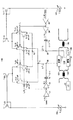
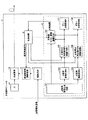
図28は、周波数特性調整回路10と電流条件モニタ回路30を有する光送信モジュール2の構成例を示す図である。光送信モジュール2は、光源40、光回路素子の一例である光変調器13、駆動回路11、周波数特性調整回路10、制御回路9、及び電流条件モニタ回路30を有する。送信データを表わす入力電気信号は、駆動回路11で高速の駆動信号に変換され、光変調器13に入力される。光源40から光変調器13に入射した光は駆動信号で変調され、変調された光信号が出力される。駆動回路11と光変調器13の間に挿入された周波数特性調整回路10により、駆動信号の電圧レベルに応じて電流I1または電流I2が光変調器13に供給され、光変調器13でデータ依存性のジッタが抑制されたフラットな周波数特性の変調が行われる。
FIG. 28 is a diagram showing a configuration example of an
周波数特性調整回路10から光変調器13に供給される電流値は、電流条件モニタ回路30の出力に基づいて、制御回路9によって制御される。電流条件モニタ回路30の構成と動作は、図25を参照して説明したとおりである。制御回路9はまた、電流条件モニタ回路30の比較結果に基づいて、電流条件モニタ回路30の比較用の周波数特性調整回路125と126の電流値を、周波数特性調整回路10と同様に制御する。比較器122として、オフセット調整機構付きの比較器を用いる場合は、制御回路9は、比較器122の出力に基づいてオフセット調整信号を生成して、比較器122に供給してもよい。オフセット調整機構付きの比較器として公知の回路構成を採用することができる。
The current value supplied from the frequency
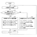
図29は、制御回路9による制御フローである。この制御フローは、光送信モジュール2の運用中に繰り返し行われるので、ループとなっている。制御回路9は、光変調器13を駆動する駆動信号の変化の都度、比較器122から比較結果を取得する(S11)。n番目(nは正の整数)の切り替わり信号(「0」と「1」の交番信号)において、連続する2つの比較タイミングT1(n)とT2(n)での比較結果が同じか否かを判断する(S12)。比較結果が異なる場合は、入力オフセットの影響は許容範囲内であるとみなして、比較結果に合わせて周波数特性調整回路10の電流値を調整する(S13)。ダミー光変調器Aに加えられる基準信号の電圧をVref、ダミー光変調器Bに加えられるシフト信号の電圧をVshiftとする。時刻T1(n)でVref>Vshift、時刻T2(n)でVref<Vshiftならば、周波数特性調整回路10の電流I1を上げるか、または電流I2を下げる制御を行う。時刻T1(n)でVre<Vshift、時刻T2(n)でVref>Vshiftならば、周波数特性調整回路10の電流I1を下げるか、または電流I2を上げる制御を行う。
FIG. 29 is a control flow by the
比較タイミングT1(n)とT2(n)で比較結果が同じ場合は(S12でYES)、入力オフセットが許容範囲を超えるとみなして、比較結果に合わせて比較器122のオフセットを調整する(S14)。具体的には、時刻T1(n)、T2(n)ともにVre>Vshiftならば、時刻T2(n)でVref<Vshiftとなる方向に比較器122のオフセット電圧を制御する。時刻T1(n)、T2(n)ともにVre<Vshiftならば、時刻T2(n)でVref>Vshiftとなる方向に比較器122のオフセット電圧を制御する。
If the comparison results are the same at the comparison timings T1 (n) and T2 (n) (YES in S12), it is considered that the input offset exceeds the allowable range, and the offset of the
ステップS13またはS14の調整が終わると、nをインクリメントしてステップS11に戻り、次の入力信号値の切り替わりのタイミング(n+1)で比較器122の出力を取得する。この制御方法により、光源40から出力される連続光は、光変調器13で周波数特性がフラットな変調を受け、データ依存性のジッタを生じさせずに高速動作が実現できる。
<光トランシーバへの適用>
When the adjustment in step S13 or S14 is completed, n is incremented and the process returns to step S11, and the output of the
<Application to optical transceivers>
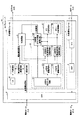
図30は、実施形態の周波数特性調整回路10を適用した光送信モジュール2Aと、これを用いた光トランシーバ1Aの概略図である。
FIG. 30 is a schematic diagram of an
光トランシーバ1Aは、光送信モジュール2Aと、光受信モジュール3と、クロックデータリカバリ(CDR:Clock Data Recovery)4を有する。光送信モジュール2Aは、図28を参照して説明した構成を有する。制御回路9は、電流条件モニタ回路30の出力に基づいて、周波数特性調整回路10から光変調器13に供給される電流I1と電流I2を調整する。電流条件モニタ回路30は、図25を参照して説明した構成と動作を有する。
The
光受信モジュール3は、フォトダイオード(PD)等の受光素子を有する光/電気(O/E)変換部7と、増幅器8を有する。増幅器(AMP)8は、たとえばPDから出力される電流を電圧に変換するトランスインピーダンスアンプ(TIA)と、TIAの出力をCDRに適した電圧レベルに増幅するリニアアンプとを含む。
The
DSP(デジタル信号プロセッサ)等の外部の信号処理回路から入力されるデータ信号は、CDR4で波形整形されて駆動回路11に入力される。駆動回路11は、入力データに基づいて高速の駆動信号を生成して、光変調器13に入力する。光変調器13は、LD40からの光を駆動信号で変調して光信号を出力する。
The data signal input from an external signal processing circuit such as a DSP (digital signal processor) is waveform-shaped by CDR4 and input to the
駆動回路11と光変調器13の間に配置される周波数特性調整回路10は、キャパシタ12と電流供給回路14を有し(図6参照)、駆動信号レベルに応じて調整用の電流I1またはI2を光変調器13に供給する。周波数特性調整回路10を挿入することで動作帯域を拡張し、追加の電源電圧や負電圧の生成なしに、イコライズ回路の機能を実現できる。さらに、入力データに応じて光変調器13に供給する電流量を切り替えることで、光変調器13の電荷-電圧特性または容量-電圧特性の非線形性が補償され、低電圧で高速駆動する場合でも良好な応答特性を得ることができる。中周波数から高周波数にかけての特性変動が抑制される結果、符号間干渉を低減できるという効果も奏する。
The frequency
周波数特性調整回路10から光変調器13に供給される電流の値は、電流条件モニタ回路30の出力に基づいて、制御回路9により図29の方式で制御される。図29の方式で電流制御を行うことで、周波数特性調整回路10から光変調器13に供給される電流I1とI2の値を、式(4)〜(6)の条件が成り立つように調整することができる。あるいは、後述の構成を採用することで、周波数特性調整回路から光変調器等の光回路素子に供給される電流IM1、IL1、IM2、IL2の値を式(7)〜(11)が成り立つように、あるいは、I00、I01、I10、I11の値を式(12)〜(16)が成り立つように、制御することができる。実施例7の構成を用いる場合は、制御信号S1〜Smも制御回路9から周波数特性調整回路10に供給され、設計された帯域特性の実現に寄与する。
The value of the current supplied from the frequency
受信側では、受信された光信号は電気信号に変換され、適切なレベルに増幅された後にCDR4に入力される。CDR4は、受信信号からデータを識別し再生して、データ信号をデジタル信号プロセッサに出力する。 On the receiving side, the received optical signal is converted into an electrical signal, amplified to an appropriate level, and then input to the CDR4. The CDR4 identifies data from the received signal, reproduces the data, and outputs the data signal to the digital signal processor.
光源40と、光変調器13と、ダミー光変調器127,128は、シリコンフォトニクス技術でひとつのチップに形成されていてもよい。駆動回路11、比較用駆動回路123及び124、周波数特性調整回路10、比較用の周波数特性調整回路125,126は、ひとつの集積(IC)チップに形成されていてもよい。なお、光送信モジュール2の温度制御やLD40の駆動電流の制御は本発明と直接関係がないので、これらの制御部の図示は省略されている。
The
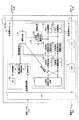
図31は、図30の光トランシーバ1Aでばらつきを抑制するための対策を示す図である。光送信モジュール2Aのダミー光変調器127と128の間にばらつきがある場合は、比較用信号生成回路121から比較用駆動回路123と124に入力される信号(基準信号とシフト信号)を切り替えて、切り替え前と切り替え後の電流調整値の平均をとる手法を用いてもよい。これにより、ダミー光変調器127と128の間の製造ばらつき等に対処することができる。
FIG. 31 is a diagram showing measures for suppressing variation in the
図32は、光トランシーバの変形例として、光トランシーバ1Bを示す。光トランシーバ1Bは、一度の変調で2ピットを伝達するPAM4(Power Amplitude Modulation-4:4値パルス振幅変調)方式の光トランシーバである。光トランシーバ1Bは、たとえば実施例4(図15)のように、MZ型光変調器の各光導波路に分割された信号電極を配置して、下位ビット(LSB)と上位ビットを個別に変調する構成に適用される。 FIG. 32 shows an optical transceiver 1B as a modification of the optical transceiver. The optical transceiver 1B is a PAM4 (Power Amplitude Modulation-4: 4-value pulse amplitude modulation) type optical transceiver that transmits two pits with one modulation. In the optical transceiver 1B, for example, as in the fourth embodiment (FIG. 15), a divided signal electrode is arranged in each optical waveguide of the MZ type optical modulator, and the lower bit (LSB) and the upper bit are modulated individually. Applies to the configuration.
光トランシーバ1Bの光送信モジュール2Bは、LSB用の駆動回路11Lと、MSB用の駆動回路11Mを有し、下位ビットを表わす電気信号と、上位ビットを表わす電気信号が、それぞれ駆動回路11Lと駆動回路11Mに入力される。周波数特性調整回路10Lは、駆動回路11Lから供給される駆動電圧のレベルに応じて、LSB変調用の光変調器13Lに電流I1またはI2を供給する。周波数特性調整回路10Mは、駆動回路11Mから供給される駆動電圧のレベルに応じて、MSB変調用の光変調器13Mに電流I1またはI2を供給する。光源40から出力される光は、光変調器13Lと光変調器13Mで変調を受け、4ビットの変調光信号が生成され、出力される。
The optical transmission module 2B of the optical transceiver 1B has a
制御回路9は、電流条件モニタ回路30の出力に基づいて、周波数特性調整回路10Mから光変調器13Mに供給される電流値IM1及びIM2と、周波数特性調整回路10Lから光変調器13Lに供給される電流IL1及びIL2を制御する。比較器122がオフセット調整機構付きの場合は、比較器122の入力オフセットをフィードバック調整してもよい。図31と同様に、制御回路9は比較用駆動回路123と124に供給される信号を切り替えてダミー光変調器127、128間のばらつきを低減してもよい。
The
図33は、PAM4光トランシーバの別の例である光トランシーバ1Cを示す。光トランシーバ1Cは、実施例5(図16)または実施例6(図17)のように、MZ型の光変調器に一対の信号電極を配置してPAM4変調方式で2ビットの変調信号を生成する構成に適用される。下位ビットLSBと上位ビットMSBの夫々に対して駆動回路11Lと11Mが配置され、駆動回路11Lと11Mの各々に対応して周波数特性調整回路10Lと10Mが設けられる。周波数特性調整回路10Lと10Mは、対応するビットの光変調について、駆動電圧のレベルに応じた電流値を供給しフラットな周波数特性での光変調を実現する。
FIG. 33 shows an optical transceiver 1C, which is another example of a PAM4 optical transceiver. In the optical transceiver 1C, as in Example 5 (FIG. 16) or Example 6 (FIG. 17), a pair of signal electrodes are arranged in an MZ type optical modulator to generate a 2-bit modulated signal by a PAM4 modulation method. Applies to the configuration to be.
制御回路9は、電流条件モニタ回路30の出力に基づいて、周波数特性調整回路10Mから光変調器13Mに供給される電流値IM1及びIM2と、周波数特性調整回路10Lから光変調器13Lに供給される電流IL1及びIL2を制御する。比較器122がオフセット調整機構付きの場合は、比較器122の入力オフセットをフィードバック調整してもよい。図31と同様に、制御回路9は比較用駆動回路123と124に供給される信号を切り替えてダミー光変調器127、128間のばらつきを低減してもよい。
The
図32と図33の構成は、3ビット以上のデータ変調にも適用される。nビットのデータ変調の場合に、n個の駆動回路11に対応してn個の周波数特性調整回路10を設け、各ビットの入力値(「0」または「1」)に応じて光変調器13等の光回路素子に供給する電流値を制御して、周波数特性を調整する。
<電流制御の変形例1>
The configurations of FIGS. 32 and 33 also apply to data modulation of 3 bits or more. In the case of n-bit data modulation, n frequency
<Modification example 1 of current control>
上述した電流制御により、入力データ値に応じて周波数特性調整回路10から適切なレベルの電流I1またはI2が供給される。しかし比較器122で比較される信号の電位が小さく、1mV以下となる場合もあり、比較器122のオフセット調整にサブmVの分解能が必要になる場合もある。比較器122の機能構成を改良してサブmVの分解能を実現することは不可能ではないが、難しい。そこで、電流制御の変形例として、比較用の信号の差分を増幅してから比較する。
By the current control described above, an appropriate level of current I 1 or I 2 is supplied from the frequency
図34は、電流制御の変形例1の原理を説明する図である。図34(A)のように基準信号とシフト信号に応じて比較用の周波数特性調整回路から出力される波形を時間T1とT2で直接比較すると、信号の電位差が小さく正しい比較結果が得られない場合もあり得る。そこで、図34(B)のように反転信号を生成し、図34(C)のように非反転信号の電圧波形の差動増幅値と、反転信号の電圧波形の差動増幅値を比較する。
FIG. 34 is a diagram illustrating the principle of
図34(B)において、基準信号の反転信号とシフト信号の反転信号を生成し、非反転信号と反転信号のそれぞれについて比較用の周波数特性調整回路からの出力波形を得る。図34(C)の細い実線は、基準信号とシフト信号の入力に応じた比較用の周波数特性調整回路の出力を差動増幅した波形、一点鎖線は、反転基準信号と反転シフト信号の入力に応じた比較用の周波数特性調整回路の出力を差動増幅した波形である。 In FIG. 34 (B), an inverted signal of a reference signal and an inverted signal of a shift signal are generated, and output waveforms from a frequency characteristic adjustment circuit for comparison are obtained for each of the non-inverting signal and the inverted signal. The thin solid line in FIG. 34 (C) is the waveform obtained by differentially amplifying the output of the frequency characteristic adjustment circuit for comparison according to the input of the reference signal and the shift signal, and the one-point chain line is the input of the inverting reference signal and the inverting shift signal. It is a waveform obtained by differentially amplifying the output of the corresponding frequency characteristic adjustment circuit for comparison.
時間T1とT2において、非反転の基準信号とシフト信号に基づく応答波形が一致していれば、差動増幅値はゼロになる、同様に、反転基準信号と反転シフト信号に基づく応答波形が一致していれば、差動増幅値はゼロになる。そこで、時刻T1、T2において、非反転信号の差動増幅値と、反転信号の差動増幅値の差がゼロに近づくように、周波数特性調整回路から供給される電流値を制御する。非反転信号の差動増幅値と、反転信号の差動増幅値の電位は増幅されているため、分解能を高めて精度良く比較することができる。 At times T1 and T2, if the non-inverting reference signal and the response waveform based on the shift signal match, the differential amplification value becomes zero. Similarly, the response waveform based on the inverting reference signal and the inverting shift signal is one. If so, the differential amplification value will be zero. Therefore, at times T1 and T2, the current value supplied from the frequency characteristic adjustment circuit is controlled so that the difference between the differential amplification value of the non-inverting signal and the differential amplification value of the inverting signal approaches zero. Since the potentials of the differential amplification value of the non-inverting signal and the differential amplification value of the inverting signal are amplified, the resolution can be improved and the comparison can be performed with high accuracy.
基準信号がシフト信号よりも大きい場合は差分はプラス側に増幅され、基準信号がシフト信号よりも小さい場合は差分はマイナス側に増幅される。反転基準信号が反転シフト信号よりも大きい場合は差分はプラス側に増幅され、反転基準信号が反転シフト信号よりも小さい場合は差分はマイナス側に増幅される。したがって、基準信号がシフト信号よりも大きい場合は、基準信号とシフト信号の差動増幅値と反転信号と反転シフト信号の差動増幅値との比較結果はプラスになる。基準信号がシフト信号よりも小さい場合は、基準信号とシフト信号の差動増幅値と反転信号と反転シフト信号の差動増幅値との比較結果はマイナスになる。比較結果の符号によって、電流制御の方向を知ることができる。 When the reference signal is larger than the shift signal, the difference is amplified to the plus side, and when the reference signal is smaller than the shift signal, the difference is amplified to the minus side. When the inverting reference signal is larger than the inverting shift signal, the difference is amplified to the plus side, and when the inverting reference signal is smaller than the inverting shift signal, the difference is amplified to the minus side. Therefore, when the reference signal is larger than the shift signal, the comparison result between the differential amplification value of the reference signal and the shift signal and the differential amplification value of the inverting signal and the inverting shift signal is positive. When the reference signal is smaller than the shift signal, the comparison result between the differential amplification value of the reference signal and the shift signal and the differential amplification value of the inverting signal and the inverting shift signal is negative. The direction of current control can be known from the sign of the comparison result.
図35は、図34の原理を実現する電流条件モニタ回路330Aの概略図である。電流条件モニタ回路330Aは、比較用信号生成回路321Aと、比較器322Aと、比較用駆動回路123、124、323、324と、比較用の周波数特性調整回路125、126、325、326と、ダミー光変調器127、128、327、328と、差動増幅器331及び332を有する。比較用信号生成回路321Aは、光変調用の駆動回路11に入力されるデータ信号と同期する基準信号と反転基準信号、基準信号と反転基準信号をそれぞれ時間τだけシフトさせたシフト信号と反転シフト信号、及び比較タイミング信号を生成する。基準信号が立ち上がった後にシフト信号が立ち上がり、基準信号が立ち下がった後にシフト信号が立ち下がる。反転基準信号が立ち下がった後に反転シフト信号が立ち下がり、反転基準信号が立ち上がった後に反転シフト信号が立ちあがる。
FIG. 35 is a schematic diagram of a current
基準信号は比較用駆動回路123(駆動回路A)に入力され、駆動回路Aで生成された比較用の駆動信号が、比較用の周波数特性調整回路125(周波数特性調整回路A)に入力される。周波数特性調整回路Aは、比較用の駆動信号の電圧レベルに応じて、電流I1または電流I2をダミー光変調器127(ダミー光変調器A)に供給する。シフト信号は比較用駆動回路124(駆動回路B)に入力され、駆動回路Bで生成された駆動信号が、比較用の周波数特性調整回路126(周波数特性調整回路B)に入力される。周波数特性調整回路Bは、比較用の駆動信号の電圧レベルに応じて、電流I1または電流I2をダミー光変調器128(ダミー光変調器B)に供給する。 The reference signal is input to the comparison drive circuit 123 (drive circuit A), and the comparison drive signal generated by the drive circuit A is input to the comparison frequency characteristic adjustment circuit 125 (frequency characteristic adjustment circuit A). .. The frequency characteristic adjusting circuit A supplies the current I 1 or the current I 2 to the dummy optical modulator 127 (dummy optical modulator A) according to the voltage level of the driving signal for comparison. The shift signal is input to the comparison drive circuit 124 (drive circuit B), and the drive signal generated by the drive circuit B is input to the comparison frequency characteristic adjustment circuit 126 (frequency characteristic adjustment circuit B). The frequency characteristic adjusting circuit B supplies the current I 1 or the current I 2 to the dummy optical modulator 128 (dummy optical modulator B) according to the voltage level of the driving signal for comparison.
反転基準信号は比較用駆動回路323(駆動回路C)に入力され、駆動回路Cで生成された比較用の反転駆動信号が、比較用の周波数特性調整回路325(周波数特性調整回路C)に入力される。周波数特性調整回路Cは、比較用の反転駆動信号の電圧レベルに応じて、電流I1または電流I2をダミー光変調器327(ダミー光変調器C)に供給する。反転シフト信号は比較用駆動回路324(駆動回路D)に入力され、駆動回路Dで生成された反転駆動信号が、比較用の周波数特性調整回路326(周波数特性調整回路D)に入力される。周波数特性調整回路Dは、比較用の反転駆動信号の電圧レベルに応じて、電流I1または電流I2をダミー光変調器328(ダミー光変調器D)に供給する。 The inverting reference signal is input to the comparison drive circuit 323 (drive circuit C), and the comparison inverting drive signal generated by the drive circuit C is input to the comparison frequency characteristic adjustment circuit 325 (frequency characteristic adjustment circuit C). Will be done. The frequency characteristic adjusting circuit C supplies the current I 1 or the current I 2 to the dummy optical modulator 327 (dummy optical modulator C) according to the voltage level of the inverting drive signal for comparison. The inverting shift signal is input to the comparison drive circuit 324 (drive circuit D), and the inverting drive signal generated by the drive circuit D is input to the comparison frequency characteristic adjustment circuit 326 (frequency characteristic adjustment circuit D). The frequency characteristic adjustment circuit D supplies the current I 1 or the current I 2 to the dummy optical modulator 328 (dummy optical modulator D) according to the voltage level of the inverting drive signal for comparison.
比較用駆動回路123、124、323、及び324は、実施例1〜7で用いられる駆動回路11と同じ構成である。比較用の周波数特性調整回路125、126、325、及び326は、実施例1〜7で用いられる周波数特性調整回路10(または10A〜10G)と同じ構成である。ダミー光変調器127、128、327、及び328は、実施例1〜7で用いられる光変調器13と同じ構成である。
The
ダミー光変調器Aに加わる電圧波形は、差動増幅器331の第1入力に接続され、ダミー光変調器Bに加わる電圧波形は、差動増幅器331の第2入力に接続されて、差動増幅器331から差動増幅結果が比較器322Aに入力される。ダミー光変調器Cに加わる電圧波形は、差動増幅器332の第1入力に接続され、ダミー光変調器Dに加わる電圧波形は、差動増幅器332の第2入力に接続されて、差動増幅器332から差動増幅結果が比較器322Aに入力される
The voltage waveform applied to the dummy optical modulator A is connected to the first input of the
比較器322Aは、比較タイミング信号の立ち上がりエッジで、差動増幅器331の出力波形と、差動増幅器332の出力波形を比較する。比較タイミング信号の立ち上がりエッジは、非反転の基準信号のプラス側のスパイクの後にシフト信号の電圧が一定レベルに収束する時刻T1と、マイナス側のスパイク後にシフト信号の電圧が一定レベルに収束する時刻T2を交互に示す。比較器322Aは、n−1番目の入力信号について、時刻T1(n−1)と時刻T2(n−1)で入力された2つの差動増幅波形を比較し、n番目の入力信号について、時刻T1(n)と時刻T2(n)で比較する。比較結果は、周波数特性調整回路10(または10A〜10G)の電流値を制御する制御回路に供給される。制御回路は、図29を参照して説明した制御動作を行う。
The
すなわち、時刻T1とT2で連続する2つの差動増幅値の比較結果の符号が異なる場合は、比較結果に応じて電流値I1またはI2を調整する。時刻T1で非反転の差動増幅値が反転の差動増幅値よりも大きく、時刻T2で非反転の差動増幅値が反転の差動増幅値よりも小さい場合は、電流I1を上げる、または電流I2を下げる。時刻T1で非反転の差動増幅値が反転の差動増幅値よりも小さく、時刻T2で非反転の差動増幅値が反転の差動増幅値よりも大きい場合は、電流I1を下げる、または電流I2を上げる。 That is, when the signs of the comparison results of the two consecutive differential amplification values are different at the times T1 and T2, the current values I 1 or I 2 are adjusted according to the comparison results. When the non-inverting differential amplification value is larger than the inverting differential amplification value at time T1 and the non-inverting differential amplification value is smaller than the inverting differential amplification value at time T2, the current I 1 is increased. Or lower the current I 2. If the non-inverting differential amplification value is smaller than the inverting differential amplification value at time T1 and the non-inverting differential amplification value is greater than the inverting differential amplification value at time T2, the current I 1 is reduced. Or increase the current I 2.
時刻T1とT2で連続する2つの差動増幅値の比較結果の符号が同じ場合は、比較器322Aのオフセット値を調整する。時刻T1、T2ともに非反転の差動増幅結果が反転の差動増幅結果よりも大きい場合は、時刻T2で非反転の差動増幅結果が反転の差動増幅結果よりも小さくなる方向に比較器322Aのオフセットを調整する。時刻T1、T2ともに非反転の差動増幅結果が反転の差動増幅結果よりも小さい場合は、時刻T2で非反転の差動増幅結果が反転の差動増幅結果よりも大きくなる方向に比較器322Aのオフセットを調整する。
If the sign of the comparison result of two consecutive differential amplification values at time T1 and T2 is the same, the offset value of the
図36は、比較用信号生成回路321Aの一例として、比較用信号生成回路321Aaの構成を示す。比較用信号生成回路321Aaは、比較用の駆動信号(基準信号とシフト信号)を先に作り、これらの駆動信号から比較タイミング信号と反転駆動信号(反転基準信号と反転シフト信号)を作る。クロック生成回路214の出力は、基準信号として比較用駆動回路Aに入力され、その反転信号が比較用駆動回路Cに入力される。一方、クロック生成回路214の出力は、遅延回路τ1及びτ2で遅延されてシフト信号とその反転信号が生成される。シフト信号は比較用駆動回路Bに入力され、反転シフト信号は比較用駆動回路Dに入力される。基準信号を遅延回路τ1で遅延させた信号と、シフト信号を遅延回路τ3で遅延させた信号は、XNOR(否定排他的論理和)回路215に入力されて比較タイミング信号が生成される。比較タイミング信号は比較器322Aに供給される。この構成により、比較タイミング信号の立ち上がりのタイミングで、2つの差動増幅波形を比較することができる。
FIG. 36 shows the configuration of the comparison signal generation circuit 321Aa as an example of the comparison
図37は、比較用信号生成回路321Aの別の例として、比較用信号生成回路321Abの構成を示す。比較用信号生成回路321Abでは、比較器322Aに供給される比較タイミング信号を先に作り、比較タイミング信号に基づいて、比較用の駆動信号(基準信号、シフト信号、反転基準信号、及び反転シフト信号)を生成する。クロック生成回路214の出力は、比較タイミング信号として比較器322Aに供給される。比較タイミング信号のタイミングを適切にするために、遅延τが加えられてよいが、遅延τは必須ではない。
FIG. 37 shows the configuration of the comparison signal generation circuit 321Ab as another example of the comparison
1/2分周器216は、クロック生成回路214から出力されるクロック信号に基づいて、クロック信号の立ち上がりに同期する基準信号(φ2=φ0)と、クロック信号の立下りに同期するシフト信号(φ3=φ0+π/2)と、クロック信号の立ち上がりに同期する反転基準信号(φ2=φ0+π)と、クロック信号の立下りに同期する反転シフト信号(φ3=φ0+3π/2)を生成する。基準信号は比較用駆動回路Aに供給され、シフト信号は比較用駆動回路Bに供給される。反転基準信号は比較用駆動回路Cに供給され、反転シフト信号は比較用駆動回路Dに供給される。図37の構成でも、比較タイミング信号の立ち上がりのタイミングで、2つの差動増幅波形を比較することができる。
<電流制御の変形例2>
The 1/2
<Modification example 2 of current control>
図38は、電流制御の変形例2の原理を説明する図である。差動増幅値を比較する構成では、基準信号とシフト信号の差分、及び反転基準信号と反転シフト信号の差分さえ取れればよいので、図38のように基準信号に替えて第1固定電位を用い、反転基準信号に替えて第2固定電位を用いても差動増幅比較が可能である。
FIG. 38 is a diagram illustrating the principle of
図38の例では、時刻T1での比較のために、比較用駆動回路Aの出力をHighに固定し、比較用駆動回路Bの出力はシフト波形を用いる。また、比較用駆動回路Cの出力をLowに固定し、比較用駆動回路Dの出力は反転シフト波形を用いる。シフト波形によりダミー光変調器Bに加わる電圧波形と、High電位によりダミー光変調器Aに加わる電圧波形の差分を増幅し、この差動増幅値を時間T1での比較器への一方の入力IN1として用いる。反転シフト波形によりダミー光変調器Dに加わる電圧波形と、Low電位によりダミー光変調器Cに加わる電圧波形の差分を増幅し、この差動増幅値を時間T1での比較器への他方の入力IN1xとして用いる。 In the example of FIG. 38, the output of the comparison drive circuit A is fixed to High for comparison at time T1, and the output of the comparison drive circuit B uses a shift waveform. Further, the output of the comparison drive circuit C is fixed to Low, and the output of the comparison drive circuit D uses an inverting shift waveform. The difference between the voltage waveform applied to the dummy optical modulator B by the shift waveform and the voltage waveform applied to the dummy optical modulator A by the high potential is amplified, and this differential amplification value is used as one input IN1 to the comparator at time T1. Used as. The difference between the voltage waveform applied to the dummy optical modulator D by the inverting shift waveform and the voltage waveform applied to the dummy optical modulator C by the Low potential is amplified, and this differential amplification value is input to the comparator at time T1. Used as IN1x.
時刻T2での比較のために、比較用駆動回路Aの出力をHighに固定し、比較用駆動回路Dの出力は反転シフト波形を用いる。また、比較用駆動回路Cの出力をLowに固定し、比較用駆動回路Bの出力は反転シフト波形を用いる。シフト波形によりダミー光変調器Bに加わる電圧波形と、Low電位によりダミー光変調器Cに加わる電圧波形の差分を増幅し、この差動増幅値を時間T2での比較器への一方の入力IN2として用いる。反転シフト波形によりダミー光変調器Dに加わる電圧波形と、High電位によりダミー光変調器Aに加わる電圧波形の差分を増幅し、この差動増幅値を時間T2での比較器への他方の入力IN2xとして用いる。比較結果に基づく制御回路の電流制御は、変形例1で説明した制御と同様である。すなわち、T1、T2における連続する2つの比較結果が異なる場合は比較結果に応じて電流値I1またはI2を調整し、2つの比較結果が同じ場合は、差動増幅値の大小によって、比較器のオフセットを調整する。 For comparison at time T2, the output of the comparison drive circuit A is fixed to High, and the output of the comparison drive circuit D uses an inverting shift waveform. Further, the output of the comparison drive circuit C is fixed to Low, and the output of the comparison drive circuit B uses an inverting shift waveform. The difference between the voltage waveform applied to the dummy optical modulator B by the shift waveform and the voltage waveform applied to the dummy optical modulator C by the Low potential is amplified, and this differential amplification value is used as one input IN2 to the comparator at time T2. Used as. The difference between the voltage waveform applied to the dummy optical modulator D by the inverting shift waveform and the voltage waveform applied to the dummy optical modulator A by the High potential is amplified, and this differential amplification value is input to the comparator at time T2. Used as IN2x. The current control of the control circuit based on the comparison result is the same as the control described in the first modification. That is, if the two consecutive comparison results in T1 and T2 are different, the current value I 1 or I 2 is adjusted according to the comparison result, and if the two comparison results are the same, the comparison is made according to the magnitude of the differential amplification value. Adjust the offset of the vessel.
この構成により、比較用駆動回路Aの電位をHigh,比較用駆動回路Cの電位をLowに固定し、かつ比較用駆動回路Bの出力(シフト信号)と比較用駆動回路Dの出力(反転シフト信号)は比較例1と同じ波形を用いることができる。図38の構成では、回路の半分(駆動回路Bと駆動回路D)だけがAC的に動作するので、消費電力を低減することができる。 With this configuration, the potential of the comparison drive circuit A is fixed to High, the potential of the comparison drive circuit C is fixed to Low, and the output of the comparison drive circuit B (shift signal) and the output of the comparison drive circuit D (inverting shift). As the signal), the same waveform as in Comparative Example 1 can be used. In the configuration of FIG. 38, since only half of the circuits (drive circuit B and drive circuit D) operate in an AC manner, power consumption can be reduced.
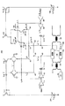
図39は、図38の原理を実現する電流条件モニタ回路330Bの概略図である。電流条件モニタ回路330Bは、比較用信号生成回路321Bと、第1の比較器322B−1と、第2の比較器322B−2を有する。電流条件モニタ回路330Bは、さらに比較用駆動回路123、124、323、324(比較用駆動回路A、B、C、Dとも標記される)と、比較用の周波数特性調整回路125、126、325、326(比較用の周波数特性調整回路A、B、C、Dとも標記される)と、ダミー光変調器127、128、327、328(ダミー光変調器A、B、C、Dとも標記される)と、差動増幅器333、334、335、336を有する。
FIG. 39 is a schematic diagram of a current condition monitor circuit 330B that realizes the principle of FIG. 38. The current condition monitor circuit 330B includes a comparison signal generation circuit 321B, a
比較用信号生成回路321Bは、比較タイミング信号1、比較タイミング信号2、光変調用の駆動回路11に入力されるデータ信号をシフトさせたシフト信号、及びその反転信号(反転シフト信号)を生成する。また、基準信号としてHigh電位の信号を生成し、反転基準信号としてLow電位の信号を生成する。High固定信号は比較用駆動回路Aに入力される。シフト信号は比較用駆動回路Bに入力される。Low固定信号は比較用駆動回路Cに入力される。反転シフト信号は比較用駆動回路Dに入力される。基準信号及び反転基準信号として電位が固定された信号が用いられるので、駆動回路Aと駆動回路Cを用いずに、High固定信号を電源電位に直結し、Low固定信号を接地(GND)電位に直結してもよい。
The comparison signal generation circuit 321B generates a
比較タイミング信号1と比較タイミング信号2は、変形例1で使用された比較タイミング信号の立ち上がりを交互に取り出した信号である。比較タイミング信号1は、比較器322B−1に入力されて時刻T1での比較に用いられる。比較タイミング信号2は、比較器322B−2に入力されて時刻T2での比較に用いられる。
The
比較用駆動回路Aから比較用の周波数特性調整回路Aを介してダミー光変調器Aに印加される電圧波形、すなわち固定電位「High」は、差動増幅器333の一方の入力に接続され、かつ差動増幅器335の一方の入力に接続される。
The voltage waveform applied from the comparison drive circuit A to the dummy optical modulator A via the comparison frequency characteristic adjustment circuit A, that is, the fixed potential “High” is connected to one input of the
比較用駆動回路Bから比較用の周波数特性調整回路Bを介してダミー光変調器Bに印加される電圧波形、すなわちシフト信号による電圧波形は、差動増幅器333の他方の入力に接続され、かつ差動増幅器334の一方の入力に接続される。
The voltage waveform applied from the comparison drive circuit B to the dummy optical modulator B via the comparison frequency characteristic adjustment circuit B, that is, the voltage waveform due to the shift signal is connected to the other input of the
比較用駆動回路Cから比較用の周波数特性調整回路Cを介してダミー光変調器Cに印加される電圧波形、すなわち固定電位「Low」は、差動増幅器334の他方の入力に接続され、かつ差動増幅器336の一方の入力に接続される。
The voltage waveform applied from the comparison drive circuit C to the dummy optical modulator C via the comparison frequency characteristic adjustment circuit C, that is, the fixed potential “Low” is connected to the other input of the
比較用駆動回路Dから比較用の周波数特性調整回路Dを介してダミー光変調器Dに印加される電圧波形、すなわち反転シフト信号による電圧波形は、差動増幅器335の他方の入力と、差動増幅器336の他方の入力に接続される。
The voltage waveform applied from the comparison drive circuit D to the dummy optical modulator D via the comparison frequency characteristic adjustment circuit D, that is, the voltage waveform due to the inverting shift signal, is differential from the other input of the
差動増幅器333と差動増幅器336、比較タイミング信号1の立ち上がりでそれぞれ差動増幅値IN1とIN1xを出力する。差動増幅値IN1及びIN1xは比較器322B−1に入力される。比較器322B−1の比較結果は時刻T1の比較結果1として制御回路に出力される。
The differential amplification values IN1 and IN1x are output at the rising edge of the
差動増幅器334と差動増幅器335は、比較タイミング信号2の立ち上がりでそれぞれ差動増幅値IN2とIN2xを出力する。差動増幅値IN2及びIN2xは比較器322B−2に入力される。比較器322B−2の比較結果は時刻T2の比較結果2として制御回路に出力される。この回路構成により電流条件モニタ回路330Bの消費電力を低減することができる。
The
図40は、変形例2のさらに別の回路構成として電流条件モニタ回路330Cを示す。電流条件モニタ回路330Cは、単一の比較タイミング信号と単一の比較器322Cを用い、時刻T1と時刻T2で、比較器322Cへの入力(すなわち差動増幅器333〜336の出力)をスイッチ341により切り替える。比較用駆動回路A〜Dに供給される信号の種類は図39と同じく、基準信号としてのHigh固定信号、シフト信号、反転基準信号としてのLow固定信号、及び反転シフト信号である。図39と同様に、High固定信号とLow固定信号をそれぞれ比較用駆動回路A,Cに供給する構成に替えて、電源電位と接地(GND)電位を比較用の周波数特性調整回路A及びCにそれぞれ供給してもよい。
FIG. 40 shows a current condition monitor circuit 330C as yet another circuit configuration of the second modification. The current condition monitor circuit 330C uses a single comparison timing signal and a
比較タイミング信号の立ち上がりを時刻T1の比較タイミングと時刻T2の比較タイミングとして交互に用いる。比較タイミング信号のある立ち上がりで、スイッチ341のSW1は差動増幅器333の出力に接続され、SW2は差動増幅器336の出力に接続される。この結果、時刻T1に、High固定信号とシフト信号の差動増幅値と、Low固定信号と反転シフト信号の差動増幅値が比較器322Cに供給される。
The rising edge of the comparison timing signal is alternately used as the comparison timing at time T1 and the comparison timing at time T2. At the rising edge of the comparison timing signal, SW1 of
比較タイミング信号の次の立ち上がりで、スイッチ341のSW1は差動増幅器334の出力に接続され、SW2は差動増幅器335の出力に接続される。この結果、時刻T2に、Low固定信号とシフト信号の差動増幅値と、High固定信号と反転シフト信号の差動増幅値が比較器322Cに供給される。
At the next rising edge of the comparison timing signal, SW1 of
この構成により、単一の比較タイミング信号と単一の比較器322Cを用いて、図39と回路と同様の動作を実現することができる。
With this configuration, a single comparison timing signal and a
図41は、図40の構成で、スイッチ構成を比較器の内部に持たせる構成を説明する図である。図41の下段に示すスイッチ動作を比較器の内部で行うために、図41の上段に示す4つのクロック信号を用いる。 FIG. 41 is a diagram illustrating a configuration in which the switch configuration is provided inside the comparator in the configuration of FIG. 40. In order to perform the switch operation shown in the lower part of FIG. 41 inside the comparator, the four clock signals shown in the upper part of FIG. 41 are used.
CLK信号の立ち上がりで、シフト信号とHIgh固定信号との差動増幅(差動増幅器333)と、シフト信号とLow固定信号との差動増幅(差動増幅器334)が交互に行われる。CLKX信号の立下りで、反転シフト信号とLow固定信号との差動増幅(差動増幅器336の出力)、及び反転シフト信号とHigh固定信号との差動増幅(差動増幅器335の出力)が交互に行われる。CLK1は時刻T1での比較クロック、CLK2は時刻T2での比較クロックである。 At the rising edge of the CLK signal, differential amplification of the shift signal and the HIgh fixed signal (differential amplifier 333) and differential amplification of the shift signal and the Low fixed signal (differential amplifier 334) are alternately performed. At the falling edge of the CLKX signal, the differential amplification of the inverting shift signal and the Low fixed signal (output of the differential amplifier 336) and the differential amplification of the inverting shift signal and the High fixed signal (output of the differential amplifier 335) are performed. It is done alternately. CLK1 is a comparison clock at time T1, and CLK2 is a comparison clock at time T2.
図42は、図41に示す4つのクロック信号CLK、CLKX、CLK1、及びCLK2を用いたスイッチング機能を内蔵する比較器322Dの回路構成例を示す。CLKとCLK1がHigh、CLKXとCLK2がLowのとき、IN1とIN1Xに現れる電圧値に応じて電流が引き抜かれ、IN1がHigh、IN1XがLowの時は、NがNXより早く電位が下がり、OUTに接続されたNMOSより、OUTXに接続されたNMOSの方が強く電流を引く抜くので、結果としてがOUTがHigh、OUTXがLowとなる。IN1がLow、IN1XがHighの時はその逆でOUTがLow、OUTXがHighとなる。CLKとCLK2がHigh、CLKXとCLK1がLowのとき、IN2とIN2Xに現れる電圧値に応じて電流が引き抜かれIN2がHigh、IN2XがLowの時は、NがNXより早く電位が下がり、OUTに接続されたNMOSより、OUTXに接続されたNMOSの方が強く電流を引く抜くので、結果としてがOUTがHigh、OUTXがLowとなる。IN2がLow、IN2XがHighの時はその逆でOUTがLow、OUTXがHighとなる。この構成により、基準信号として固定電位の信号を用いつつ、単一の比較器で時刻T1、T2における差動増幅値の比較を実現することができる。
FIG. 42 shows a circuit configuration example of a
図43は、周波数特性調整回路10と電流条件モニタ回路330を有する光送信モジュール302の構成例を示す図である。図43の例では、電流制御の変形例1で説明した電流条件モニタ回路330Aを用いているが、電流制御の変形例2の電流条件モニタ回路330Bまたは330Cを用いてもよい。
FIG. 43 is a diagram showing a configuration example of an
光送信モジュール302は、光源40、光回路素子の一例である光変調器13、駆動回路11、周波数特性調整回路10、制御回路9、及び電流条件モニタ回路330を有する。送信データを表わす入力電気信号は、駆動回路11で高速の駆動信号に変換され、光変調器13に入力される。光源40から光変調器13に入射した光は駆動信号で変調されて、変調された光信号が出力される。駆動回路11と光変調器13の間に挿入された周波数特性調整回路10により、駆動信号の電圧レベルに応じて電流I1または電流I2が光変調器13に供給され、光変調器13でデータ依存性のジッタが抑制されたフラットな周波数特性の変調が行われる。
The
周波数特性調整回路10から光変調器13に供給される電流値は、電流条件モニタ回路330の出力、すなわち差動増幅器331の出力と差動増幅器332の出力の比較結果に基づいて、制御回路9により制御される。電流条件モニタ回路330の構成と動作は、図34〜37を参照して説明したとおりである。電流条件モニタ回路330として変形例2の回路を用いる場合の構成と動作は、図38〜図42を参照して説明したものとなる。
The current value supplied from the frequency
電流条件モニタ回路330は、差動増幅出力に基づいて比較を行っているので高い分解能で正確に比較結果を出力することができる。図制御回路9は、電流条件モニタ回路330の比較結果に基づいて、電流条件モニタ回路330の比較用の周波数特性調整回路125、126、325、326から供給される電流の値を、周波数特性調整回路10に対する制御と同様に制御する。比較器322として、オフセット調整機構付きの比較器を用いる場合は、制御回路9は、比較器122の出力に基づいてオフセット調整信号を生成して比較器322に供給してもよい。オフセット調整機構付きの比較器として公知の回路構成を採用することができる。
Since the current
図44は、図43の光送信モジュール302を用いた光トランシーバ301の概略図である。光トランシーバ301は、光送信モジュール2Aに替えて光送信モジュール302を用いることを除いて、図30の光トランシーバ1Aと同じである。光トランシーバ301は、光送信モジュール302と、光受信モジュール3と、クロックデータリカバリ(CDR:Clock Data Recovery)4を有し、光受信モジュール3とCDR4の構成と動作は、図30を参照して説明したとおりである。
FIG. 44 is a schematic diagram of an
光送信モジュール302は、電流条件モニタ回路330として図35の電流条件モニタ回路330Aの構成を採用しているが、電流制御の変形例2の電流条件モニタ回路330Bまたは330Cも適用可能であることは上述した通りである。
The
駆動回路11と光変調器13の間に配置される周波数特性調整回路10は、キャパシタ12と電流供給回路14を有し(図6参照)、駆動信号レベルに応じて調整用の電流I1またはI2を光変調器13に供給する。周波数特性調整回路10を挿入することで動作帯域を拡張し、追加の電源電圧や負電圧の生成なしに、イコライズ回路の機能を実現できる。さらに、入力データに応じて光変調器13に供給する電流量を切り替えることで、光変調器13の電荷-電圧特性または容量-電圧特性の非線形性が補償され、低電圧で高速駆動する場合でも良好な応答特性を得ることができる。中周波数から高周波数にかけての特性変動が抑制される結果、符号間干渉を低減できる。
The frequency
周波数特性調整回路10から光変調器13に供給される電流の値は、電流条件モニタ回路330の出力に基づいて、制御回路9により制御される。電流条件モニタ回路330の出力は、差動増幅器331の出力(基準波形とシフト波形の差動増幅値)と、差動増幅器332の出力(反転基準波形と反転シフト波形の差動増幅値)の比較結果である。差動増幅器331と差動増幅器332の出力を用いて比較を行うことで、小さな電圧差を分解能良く検知し、入力駆動信号の値に応じた電流値I1とI2の調整を精度良く行うことができる。
The value of the current supplied from the frequency
図45は、図44の光トランシーバの変形例として光トランシーバ301Aを示す。光トランシーバ301Aの構成は、図31の光トランシーバ1Aの構成に対応し、電流条件モニタ回路330のばらつきを抑制する構成を有する。光送信モジュール302Aのダミー光変調器127と128の間、及び/またはダミー光変調器327と328の間にばらつきがある場合、比較用信号生成回路121から比較用駆動回路123と124に入力される信号(基準信号とシフト信号)を切り替える。また、比較用信号生成回路121から比較用駆動回路323と324に入力される信号(反転基準信号と反転シフト信号)を切り替える。信号の入力経路の切り替えは、制御回路9によって行われる。切り替え前と切り替え後の電流調整値の平均をとることで、ダミー光変調器127と128の間、及び/またはダミー光変調器327と328の間の製造ばらつき等に起因する処理誤差を解消することができる。
FIG. 45 shows an optical transceiver 301A as a modification of the optical transceiver of FIG. 44. The configuration of the optical transceiver 301A corresponds to the configuration of the
図46は、光トランシーバの変形例として光トランシーバ301Bを示す。光トランシーバ301Bの構成は、図32の光トランシーバ1Bの構成に対応し、一度の変調で2ピットを伝達するPAM4(Power Amplitude Modulation-4:4値パルス振幅変調)方式の光伝送を行う。光トランシーバ301Bは、たとえば実施例4(図15)のように、MZ型の光変調器の各光導波路に分割された信号電極を配置して、下位ビット(LSB)と上位ビットを個別に変調する構成に適用される。図46のPAM4方式の光変調動作は、図32を参照して述べたとおりである。 FIG. 46 shows an optical transceiver 301B as a modification of the optical transceiver. The configuration of the optical transceiver 301B corresponds to the configuration of the optical transceiver 1B of FIG. 32, and performs PAM4 (Power Amplitude Modulation-4: 4-value pulse amplitude modulation) optical transmission that transmits two pits with one modulation. In the optical transceiver 301B, for example, as in the fourth embodiment (FIG. 15), a divided signal electrode is arranged in each optical waveguide of the MZ type optical modulator, and the lower bits (LSB) and the upper bits are individually modulated. Applies to the configuration to be. The optical modulation operation of the PAM4 method of FIG. 46 is as described with reference to FIG. 32.
図47は、PAM4光トランシーバの別の例として光トランシーバ301Cを示す。光トランシーバ301Cの構成は、図33の光トランシーバ1Cの構成に対応し、MZ型の光変調器13Dに一対の信号電極を配置してPAM4変調方式で2ビットの変調信号を生成する。
FIG. 47 shows an optical transceiver 301C as another example of a PAM4 optical transceiver. The configuration of the optical transceiver 301C corresponds to the configuration of the optical transceiver 1C of FIG. 33, and a pair of signal electrodes are arranged on the MZ type
図46と図47の構成で、制御回路9は電流条件モニタ回路330の出力に基づいて、周波数特性調整回路10Mから光変調器13M(または光変調器13D)に供給される電流値IM1及びIM2を制御し、周波数特性調整回路10Lから光変調器13L(または光変調器13D)に供給される電流IL1及びIL2を制御する。図46と図47の構成は、3ビット以上のデータ変調にも適用される。nビットのデータ変調の場合に、n個の駆動回路11に対応してn個の周波数特性調整回路10を設け、各ビットの入力値(「0」または「1」)に応じて光変調器13等の光回路素子に供給する電流値を制御して、周波数特性を調整する。
In the configuration of FIGS. 46 and 47, the control circuit 9 has a current value IM1 and a current value IM1 supplied from the frequency
以上述べたように、実施形態の周波数特性調整回路を用いることで、低い電圧で従来構成のイコライズ回路と同等の機能を果たすことができる。すなわち、高電圧や負電圧を用いずに光変調器やレーザダイオード等の光回路素子の動作帯域を拡張して、高速駆動を可能にする。さらに、入力データに応じて光回路素子に供給する電流を変えることで、接合容量のように電圧依存性が非線形な要素を含む場合でも周波数特性の変動を抑制することができる。副次的な効果として、データ依存性のジッタである符号間干渉を低減できる。また、駆動回路とキャパシタCFの組を複数設けて全部または一部の組で出力状態をアクティブとHigh-Zの間で選択可能にすることで、設計された帯域特性を実現することができる。 As described above, by using the frequency characteristic adjustment circuit of the embodiment, it is possible to achieve the same function as the equalization circuit of the conventional configuration at a low voltage. That is, the operating band of an optical circuit element such as an optical modulator or a laser diode is expanded without using a high voltage or a negative voltage to enable high-speed driving. Furthermore, by changing the current supplied to the optical circuit element according to the input data, it is possible to suppress fluctuations in the frequency characteristics even when an element having a non-linear voltage dependence such as a junction capacitance is included. As a side effect, intersymbol interference, which is a data-dependent jitter, can be reduced. Further, a set output state to a plurality arranged in all or some combination of the drive circuit and the capacitor C F that it allows selection between the active and High-Z, it is possible to realize a band characteristic designed ..
実施例では、駆動回路の出力ノードから供給される電圧と駆動回路の中間ノードから取り出される電圧を用いているが、駆動回路への入力ノードから取り出される電圧を用いてもよい。入力されるデータ信号の値を反映する電圧であれば、任意のノードからの電圧を用いることができる。 In the embodiment, the voltage supplied from the output node of the drive circuit and the voltage taken out from the intermediate node of the drive circuit are used, but the voltage taken out from the input node to the drive circuit may be used. A voltage from any node can be used as long as the voltage reflects the value of the input data signal.
入力駆動信号値に応じて周波数特性調整回路10から光回路素子(光変調器、面発光レーザ等)に供給される電流値を、電流制御の実施例、変形例1、または変形例2の構成と手法で制御することで、最適な電流条件が維持され周波数特性の変動が抑制される。
The current value supplied from the frequency
電流制御の実施例、変形例1、及び変形例2は、実施例1〜7の周波数特性調整回路10A〜10Gのいずれにも適用可能である。
The current control embodiment,
以上、本発明の例示的な実施の形態の周波数特性調整回路、これを用いた光送信モジュール、及び光トランシーバについて説明したが、本発明は、具体的に開示された実施の形態に限定されるものではなく、特許請求の範囲から逸脱することなく、種々の変形や変更が可能である。
以上の実施の形態に関し、さらに以下の付記を開示する。
(付記1)
光回路素子と前記光回路素子を駆動する駆動回路の間に配置される回路であって、
前記駆動回路の出力に接続されるキャパシタと、
前記駆動回路で生成される電圧によって制御される電流供給回路と、
を有し、
前記電流供給回路は、前記駆動回路から受け取る電圧に応じて異なる電流値の電流を前記光回路素子に供給する、
ことを特徴とする周波数特性調整回路。
(付記2)
前記電流供給回路は、第1の電流を生成する第1の電流源と、前記第1の電流と異なる第2の電流を生成する第2の電流源と、を有し、
前記駆動回路から第1レベルの電圧が印加されたときに前記第1の電流を供給し、前記駆動回路から第2レベルの電圧が印加されたときに前記第2の電流を供給することを特徴とする付記1に記載の周波数特性調整回路。
(付記3)
前記電流供給回路は、第1の電流を生成する第1の電流源と、差電流を生成する第2の電流源と、を有し、
前記駆動回路から第1レベルの電圧を受け取ったときに前記第1の電流を供給し、前記駆動回路から第2レベルの電圧を受け取ったときに前記第1の電流と前記差電流を足し合わせた第2の電流を供給することを特徴とする付記1に記載の周波数特性調整回路。
(付記4)
前記電流供給回路は、前記第1の電流源と前記キャパシタの間に接続される第1スイッチと、前記第2の電流源と前記キャパシタの間に接続される第2スイッチを有し、
前記第1スイッチと前記第2スイッチは、前記駆動回路の出力に接続されていることを特徴とする付記2または3に記載の周波数特性調整回路。
(付記5)
光回路素子を駆動するn個の駆動回路に対応して設けられるn個の付記1〜4のいずれか1項に記載の周波数特性調整回路、
を有し、
i番目の駆動回路の出力をVi、
前記i番目の駆動回路に対応するi番目の周波数特性調整回路が供給する電流をIi、前記i番目の周波数特性調整回路が有するキャパシタのキャパシタンスをCFiとしたときに、
前記光回路素子の電流-電圧特性をIM(VM)、前記光回路素子の電荷-電圧特性をQM(VM)、IM(VM)=ΣIiとするとき、すべてのVi、Iiの組み合わせに対して、
QM(VM)−CFi(Vi-VMi)
が等価となる、または近似するように設定されていることを特徴とする周波数特性調整回路。
(付記6)
電気信号に基づいて光信号を出力する光回路素子と、
前記光回路素子を駆動する駆動回路と、
前記光回路素子と前記駆動回路の間に配置される周波数特性調整回路であって、前記駆動回路の出力に接続されるキャパシタと、前記駆動回路で生成される電圧によって制御される電流供給回路とを有し、前記駆動回路から受け取る電圧に応じて異なる電流値の電流を前記光回路素子に供給する周波数特性調整回路と、
を有する光送信モジュール。
(付記7)
前記周波数特性調整回路の電流条件をモニタするモニタ回路と、
前記モニタ回路の出力基づいて、前記周波数特性調整回路から前記光回路素子に供給される前記電流値を調整する制御回路と、
を有することを特徴とする付記6に記載の光送信モジュール。
(付記8)
前記モニタ回路は、
前記光回路素子と同等の性能を有する1組のダミー光回路素子と、
前記ダミー光回路素子への入力駆動波形を比較する比較器と、
前記ダミー光回路素子を駆動する1組の比較用駆動回路と、
前記比較器に供給されるタイミング信号と、前記比較用駆動回路の一方に供給される基準信号と、前記比較用駆動回路の他方に供給され前記基準信号から所定時間遅延されたシフト信号を生成する信号生成回路と、
を有することを特徴とする付記7に記載の光送信モジュール。
(付記9)
前記制御回路は、前記比較器の出力が連続する2つの比較タイミングで異なる結果を示す場合に、前記周波数特性調整回路から前記光回路素子に供給される電流値を調整することを特徴とする付記8に記載の光送信モジュール。
(付記10)
前記制御回路は、前記比較器の出力が連続する2つの比較タイミングで同じ結果を示す場合に、前記比較器の入力オフセット電圧を調整することを特徴とする付記8に記載の光送信モジュール。
(付記11)
前記モニタ回路は、
前記光回路素子と同等の性能を有する第1〜第4のダミー光回路素子と、
前記第1〜第4のダミー光回路素子を駆動する第1〜第4の比較用駆動回路と、
第1のダミー光回路素子に入力される電圧波形と第2のダミー光回路素子に入力される電圧波形を差動増幅する第1の差動増幅器と、
第3のダミー光回路素子に入力される電圧波形と第4のダミー光回路素子に入力される電圧波形を差動増幅する第2の差動増幅器と
を有し、
前記信号生成回路は、前記基準信号を反転した反転基準信号と、前記シフト信号を反転した反転シフト信号をさらに生成し、
前記基準信号による駆動波形が前記第1のダミー光回路素子に入力され、前記シフト信号による駆動波形が前記第2のダミー光回路素子に入力され、前記反転基準信号による駆動波形が前記第3のダミー光回路素子に入力され、前記反転シフト信号による駆動波形が前記第4のダミー光回路素子に入力され、
前記比較器は、前記第1の差動増幅器の出力と、前記第2の差動増幅器の出力の比較結果を出力することを特徴とする付記8に記載の光送信モジュール。
(付記12)
前記基準信号は第1の固定電位信号であり、前記反転基準信号は前記第1の固定電位信号と異なる第2の固定電位信号であり、
前記モニタ回路は、第3の差動増幅器と第4の差動増幅器をさらに有し、
前記第1の差動増幅器は、前記第1の固定電位信号により駆動される第1のダミー光回路素子の入力波形と、前記シフト信号により駆動される第2のダミー光回路素子の入力波形を差動増幅し、
前記第2の差動増幅器は、前記第2の固定電位信号により駆動される第3のダミー光回路素子の入力波形と、前記反転シフト信号により駆動される第4のダミー光回路素子の入力波形を差動増幅し、
前記第3の差動増幅器は、前記第2の固定電位信号により駆動される第3のダミー光回路素子の入力波形と、前記シフト信号により駆動される第2のダミー光回路素子の入力波形を差動増幅し、
前記第4の差動増幅器は、前記第1の固定電位信号により駆動される第4のダミー光回路素子の入力波形と、前記反転シフト信号により駆動される第4のダミー光回路素子の入力波形を差動増幅し、
前記比較器は、前記第1の差動増幅器の出力と前記第2の差動増幅器の出力の比較結果を第1の時間に出力し、前記第3の差動増幅器の出力と前記第4の差動増幅器の出力の比較結果を第2の時間に出力することを特徴とする付記11に記載の光送信モジュール。
(付記13)
前記比較器は、
前記第1の差動増幅器の出力と前記第2の差動増幅器の出力を比較して前記第1の時間に第1比較結果を出力する第1比較器と、
前記第3の差動増幅器の出力と前記第4の差動増幅器の出力を比較して前記第2の時間に第2比較結果を出力する第2比較器と、
を有することを特徴とする付記12に記載の光送信モジュール。
(付記14)
前記比較器は、前記第1の時間に前記第1の差動増幅器の出力と前記第2の差動増幅器の出力を選択し、前記第2の時間に前記第3の差動増幅器の出力と前記第4の差動増幅器の出力を選択するスイッチ部を有することを特徴とする付記12に記載の光送信モジュール。
(付記15)
駆動回路と前記駆動回路の出力に接続されるキャパシタの組を複数有し、
複数の組の少なくとも一部において、前記駆動回路の出力がアクティブと高インピーダンスの間で選択可能であることを特徴とする付記6〜14のいずれか1項に記載の光送信モジュール。
(付記16)
前記駆動回路の入力にはデータ信号と制御信号が接続され、前記駆動回路は前記制御信号の値に応じて、入力された前記データ信号の値を出力するか、または出力状態が高インピーダンスとなることを特徴とする付記15に記載の光送信モジュール。
(付記17)
付記6〜16のいずれか1項に記載の光送信モジュールと、
光受信モジュールと、
を有する光トランシーバ。
Although the frequency characteristic adjustment circuit of the exemplary embodiment of the present invention, the optical transmission module using the same, and the optical transceiver have been described above, the present invention is limited to the specifically disclosed embodiments. It is not a thing, and various modifications and changes can be made without departing from the scope of claims.
The following additional notes will be further disclosed with respect to the above embodiments.
(Appendix 1)
A circuit arranged between an optical circuit element and a drive circuit for driving the optical circuit element.
The capacitor connected to the output of the drive circuit and
A current supply circuit controlled by the voltage generated by the drive circuit and
Have,
The current supply circuit supplies the optical circuit element with a current having a different current value depending on the voltage received from the drive circuit.
A frequency characteristic adjustment circuit characterized by this.
(Appendix 2)
The current supply circuit has a first current source that produces a first current and a second current source that produces a second current that is different from the first current.
It is characterized in that the first current is supplied when a first level voltage is applied from the drive circuit, and the second current is supplied when a second level voltage is applied from the drive circuit. The frequency characteristic adjustment circuit according to
(Appendix 3)
The current supply circuit has a first current source that produces a first current and a second current source that produces a differential current.
When the first level voltage is received from the drive circuit, the first level current is supplied, and when the second level voltage is received from the drive circuit, the first level current and the difference current are added. The frequency characteristic adjusting circuit according to
(Appendix 4)
The current supply circuit includes a first switch connected between the first current source and the capacitor, and a second switch connected between the second current source and the capacitor.
The frequency characteristic adjusting circuit according to
(Appendix 5)
The frequency characteristic adjusting circuit according to any one of the
Have,
The output of the i-th drive circuit is Vi,
The i-th frequency characteristic adjusting circuit for supplying current corresponding to the i th driving circuit Ii, the capacitance of the capacitor when the C Fi of the i-th frequency characteristic adjusting circuit has,
Current of the optical circuit element - the voltage characteristic I M (V M), the charge of the optical circuit element - the voltage characteristic Q M (V M), when the I M (V M) = ΣIi , all Vi, For the combination of Ii
Q M (V M) -C Fi (Vi-V Mi)
A frequency characteristic adjustment circuit characterized in that is set to be equivalent or approximate.
(Appendix 6)
An optical circuit element that outputs an optical signal based on an electrical signal,
The drive circuit that drives the optical circuit element and
A frequency characteristic adjusting circuit arranged between the optical circuit element and the drive circuit, the capacitor connected to the output of the drive circuit, and a current supply circuit controlled by a voltage generated by the drive circuit. And a frequency characteristic adjustment circuit that supplies a current with a different current value depending on the voltage received from the drive circuit to the optical circuit element.
Optical transmission module with.
(Appendix 7)
A monitor circuit that monitors the current conditions of the frequency characteristic adjustment circuit and
A control circuit that adjusts the current value supplied from the frequency characteristic adjusting circuit to the optical circuit element based on the output of the monitor circuit, and a control circuit that adjusts the current value.
The optical transmission module according to Appendix 6, wherein the module is characterized by having.
(Appendix 8)
The monitor circuit is
A set of dummy optical circuit elements having the same performance as the optical circuit element,
A comparator that compares the input drive waveform to the dummy optical circuit element, and
A set of comparative drive circuits that drive the dummy optical circuit elements,
A timing signal supplied to the comparator, a reference signal supplied to one of the comparison drive circuits, and a shift signal supplied to the other of the comparison drive circuits and delayed by a predetermined time from the reference signal are generated. Signal generation circuit and
The optical transmission module according to
(Appendix 9)
The appendix is characterized in that the control circuit adjusts the current value supplied from the frequency characteristic adjusting circuit to the optical circuit element when the outputs of the comparator show different results at two consecutive comparison timings. 8. The optical transmission module according to 8.
(Appendix 10)
The optical transmission module according to
(Appendix 11)
The monitor circuit is
The first to fourth dummy optical circuit elements having the same performance as the optical circuit element,
The first to fourth comparative drive circuits that drive the first to fourth dummy optical circuit elements, and
A first differential amplifier that differentially amplifies the voltage waveform input to the first dummy optical circuit element and the voltage waveform input to the second dummy optical circuit element, and
It has a second differential amplifier that differentially amplifies the voltage waveform input to the third dummy optical circuit element and the voltage waveform input to the fourth dummy optical circuit element.
The signal generation circuit further generates an inverting reference signal in which the reference signal is inverted and an inverting shift signal in which the shift signal is inverted.
The drive waveform by the reference signal is input to the first dummy optical circuit element, the drive waveform by the shift signal is input to the second dummy optical circuit element, and the drive waveform by the inversion reference signal is the third. It is input to the dummy optical circuit element, and the drive waveform by the inverting shift signal is input to the fourth dummy optical circuit element.
The optical transmission module according to
(Appendix 12)
The reference signal is a first fixed potential signal, and the inversion reference signal is a second fixed potential signal different from the first fixed potential signal.
The monitor circuit further comprises a third differential amplifier and a fourth differential amplifier.
The first differential amplifier has an input waveform of a first dummy optical circuit element driven by the first fixed potential signal and an input waveform of a second dummy optical circuit element driven by the shift signal. Differential amplification,
The second differential amplifier has an input waveform of a third dummy optical circuit element driven by the second fixed potential signal and an input waveform of a fourth dummy optical circuit element driven by the inverting shift signal. Is differentially amplified,
The third differential amplifier has an input waveform of a third dummy optical circuit element driven by the second fixed potential signal and an input waveform of a second dummy optical circuit element driven by the shift signal. Differential amplification,
The fourth differential amplifier has an input waveform of a fourth dummy optical circuit element driven by the first fixed potential signal and an input waveform of a fourth dummy optical circuit element driven by the inverting shift signal. Is differentially amplified,
The comparator outputs the comparison result of the output of the first differential amplifier and the output of the second differential amplifier in the first time, and outputs the output of the third differential amplifier and the fourth differential amplifier. The optical transmission module according to
(Appendix 13)
The comparator is
A first comparator that compares the output of the first differential amplifier with the output of the second differential amplifier and outputs the first comparison result at the first time.
A second comparator that compares the output of the third differential amplifier with the output of the fourth differential amplifier and outputs the second comparison result at the second time.
The optical transmission module according to
(Appendix 14)
The comparator selects the output of the first differential amplifier and the output of the second differential amplifier at the first time, and the output of the third differential amplifier at the second time. The optical transmission module according to
(Appendix 15)
It has a plurality of sets of a drive circuit and a capacitor connected to the output of the drive circuit.
The optical transmission module according to any one of Supplementary note 6 to 14, wherein the output of the drive circuit can be selected between active and high impedance in at least a part of a plurality of sets.
(Appendix 16)
A data signal and a control signal are connected to the input of the drive circuit, and the drive circuit outputs the value of the input data signal according to the value of the control signal, or the output state becomes high impedance. The optical transmission module according to Appendix 15, wherein the optical transmission module is characterized in that.
(Appendix 17)
The optical transmission module according to any one of Supplementary note 6 to 16.
Optical receiver module and
Optical transceiver with.
1A〜1C、301、301A〜301C 光トランシーバ
2、2A、2B、302、302A〜302C 光送信モジュール
3 光受信モジュール
9 制御回路
10、10A、10B、10C、10D、10E、10F、10G 周波数特性調整回路
11、11A 駆動回路
12−1、12−2 キャパシタ
13、13B、13C、13D、13F 光変調器(光回路素子)
13A レーザダイオード(光回路素子)
30、330A、330B、330C 電流条件モニタ回路(モニタ回路)
40 LD(光源)
121、321A、321B、321C、 比較用信号生成回路
122、322A、322B−1、322B−2、322C 比較器
123、124、323、324 比較用駆動回路
125、126、325、326 比較用の周波数特性調整回路
127,128、327、328 ダミー光変調器
141、147、148,241 第1の電流源
142,149、242 第2の電流源
201−1〜201−m、203−1〜203−m 出力状態可変バッファ(駆動回路)
214 クロック生成回路
331、332、333、334、335、336 差動増幅器
CF1−1〜CFm−1、CF1−2〜CFm−2、 キャパシタ
S1〜Sm 制御信号
τ1、τ2、τ3 遅延回路
1A to 1C, 301, 301A to
13A laser diode (optical circuit element)
30, 330A, 330B, 330C Current condition monitor circuit (monitor circuit)
40 LD (light source)
121, 321A, 321B, 321C, Comparison
214 clock generation circuit 331,332,333,334,335,336 differential amplifier C F1 -1~C Fm -1, C F1 -2~C Fm -2, capacitor S1~Sm control signal τ1, τ2, τ3 delay circuit
Claims (12)
前記駆動回路の出力に接続されるキャパシタと、
前記駆動回路で生成される電圧によって制御される電流供給回路と、
を有し、
前記電流供給回路は、前記駆動回路から受け取る電圧値に応じて異なる電流値の電流を選択的に前記光回路素子に供給し、
前記電流供給回路は、第1の電流を生成する第1の電流源と、前記第1の電流と異なる第2の電流を生成する第2の電流源と、を有し、
前記駆動回路から第1レベルの電圧が印加されたときに前記第1の電流を供給し、前記駆動回路から第2レベルの電圧が印加されたときに前記第2の電流を供給することを特徴とする周波数特性調整回路。 A circuit arranged between an optical circuit element and a drive circuit for driving the optical circuit element.
The capacitor connected to the output of the drive circuit and
A current supply circuit controlled by the voltage generated by the drive circuit and
Have,
The current supply circuit selectively supplies a current having a different current value according to the voltage value received from the drive circuit to the optical circuit element .
The current supply circuit has a first current source that produces a first current and a second current source that produces a second current that is different from the first current.
It is characterized in that the first current is supplied when a first level voltage is applied from the drive circuit, and the second current is supplied when a second level voltage is applied from the drive circuit. Frequency characteristic adjustment circuit.
前記駆動回路の出力に接続されるキャパシタと、
前記駆動回路で生成される電圧によって制御される電流供給回路と、
を有し、
前記電流供給回路は、前記駆動回路から受け取る電圧値に応じて異なる電流値の電流を選択的に前記光回路素子に供給し、
前記電流供給回路は、第1の電流を生成する第1の電流源と、差電流を生成する第2の電流源と、を有し、
前記駆動回路から第1レベルの電圧を受け取ったときに前記第1の電流を供給し、前記駆動回路から第2レベルの電圧を受け取ったときに前記第1の電流と前記差電流を足し合わせた第2の電流を供給することを特徴とする周波数特性調整回路。 A circuit arranged between an optical circuit element and a drive circuit for driving the optical circuit element.
The capacitor connected to the output of the drive circuit and
A current supply circuit controlled by the voltage generated by the drive circuit and
Have,
The current supply circuit selectively supplies a current having a different current value according to the voltage value received from the drive circuit to the optical circuit element.
The current supply circuit has a first current source that produces a first current and a second current source that produces a differential current.
When the first level voltage is received from the drive circuit, the first level current is supplied, and when the second level voltage is received from the drive circuit, the first level current and the difference current are added. you and supplying a second current frequency characteristic adjusting circuit.
前記第1スイッチと前記第2スイッチは、前記駆動回路の出力に接続されていることを特徴とする請求項1または2に記載の周波数特性調整回路。 The current supply circuit includes a first switch connected between the first current source and the capacitor, and a second switch connected between the second current source and the capacitor.
The frequency characteristic adjusting circuit according to claim 1 or 2 , wherein the first switch and the second switch are connected to an output of the drive circuit.
を有し、
i番目の駆動回路の出力をVi、
前記i番目の駆動回路に対応するi番目の周波数特性調整回路が供給する電流をIi、前記i番目の周波数特性調整回路が有するキャパシタのキャパシタンスをCFiとしたときに、
前記光回路素子の電流-電圧特性をIM(VM)、前記光回路素子の電荷-電圧特性をQM(VM)、IM(VM)=ΣIiとするとき、すべてのVi、Iiの組み合わせに対して、
QM(VM)−CFi(Vi-VMi)
が等価となる、または近似するように設定されていることを特徴とする周波数特性調整回路。 The frequency characteristic adjustment circuit according to any one of claims 1 to 3 , which is provided corresponding to the n drive circuits for driving the optical circuit element.
Have,
The output of the i-th drive circuit is Vi,
The i-th frequency characteristic adjusting circuit for supplying current corresponding to the i th driving circuit Ii, the capacitance of the capacitor when the C Fi of the i-th frequency characteristic adjusting circuit has,
Current of the optical circuit element - the voltage characteristic I M (V M), the charge of the optical circuit element - the voltage characteristic Q M (V M), when the I M (V M) = ΣIi , all Vi, For the combination of Ii
Q M (V M) -C Fi (Vi-V Mi)
A frequency characteristic adjustment circuit characterized in that is set to be equivalent or approximate.
前記光回路素子を駆動する駆動回路と、
前記光回路素子と前記駆動回路の間に配置される周波数特性調整回路であって、前記駆動回路の出力に接続されるキャパシタと、記駆動回路で生成される電圧によって制御される電流供給回路とを有し、前記電流供給回路は、前記駆動回路から受け取る電圧値に応じて異なる電流値の電流を選択的に前記光回路素子に供給する周波数特性調整回路と、
を有し、
前記電流供給回路は、第1の電流を生成する第1の電流源と、前記第1の電流と異なる第2の電流を生成する第2の電流源と、を有し、前記駆動回路から第1レベルの電圧が印加されたときに前記第1の電流を供給し、前記駆動回路から第2レベルの電圧が印加されたときに前記第2の電流を供給する、
光送信モジュール。 An optical circuit element that outputs an optical signal based on an electrical signal,
The drive circuit that drives the optical circuit element and
A frequency characteristic adjustment circuit arranged between the optical circuit element and the drive circuit, the capacitor connected to the output of the drive circuit, and the current supply circuit controlled by the voltage generated by the drive circuit. The current supply circuit includes a frequency characteristic adjusting circuit that selectively supplies a current having a different current value depending on the voltage value received from the drive circuit to the optical circuit element.
Have a,
The current supply circuit has a first current source that generates a first current and a second current source that generates a second current different from the first current, and is the first from the drive circuit. The first current is supplied when a one-level voltage is applied, and the second current is supplied when a second-level voltage is applied from the drive circuit.
Optical transmission module.
前記光回路素子を駆動する駆動回路と、 The drive circuit that drives the optical circuit element and
前記光回路素子と前記駆動回路の間に配置される周波数特性調整回路であって、前記駆動回路の出力に接続されるキャパシタと、記駆動回路で生成される電圧によって制御される電流供給回路とを有し、前記電流供給回路は、前記駆動回路から受け取る電圧値に応じて異なる電流値の電流を選択的に前記光回路素子に供給する周波数特性調整回路と、 A frequency characteristic adjustment circuit arranged between the optical circuit element and the drive circuit, the capacitor connected to the output of the drive circuit, and the current supply circuit controlled by the voltage generated by the drive circuit. The current supply circuit includes a frequency characteristic adjusting circuit that selectively supplies a current having a different current value depending on the voltage value received from the drive circuit to the optical circuit element.
を有し、Have,
前記電流供給回路は、第1の電流を生成する第1の電流源と、差電流を生成する第2の電流源と、を有し、前記駆動回路から第1レベルの電圧を受け取ったときに前記第1の電流を供給し、前記駆動回路から第2レベルの電圧を受け取ったときに前記第1の電流と前記差電流を足し合わせた第2の電流を供給する、The current supply circuit has a first current source that produces a first current and a second current source that produces a differential current, when a first level voltage is received from the drive circuit. The first current is supplied, and when a second level voltage is received from the drive circuit, a second current obtained by adding the first current and the difference current is supplied.
光送信モジュール。Optical transmission module.
前記光回路素子を駆動する駆動回路と、
前記光回路素子と前記駆動回路の間に配置される周波数特性調整回路であって、前記駆動回路の出力に接続されるキャパシタと、記駆動回路で生成される電圧によって制御される電流供給回路とを有し、前記電流供給回路は、前記駆動回路から受け取る電圧値に応じて異なる電流値の電流を選択的に前記光回路素子に供給する周波数特性調整回路と、
前記周波数特性調整回路の電流条件をモニタするモニタ回路と、
前記モニタ回路の出力基づいて、前記周波数特性調整回路から前記光回路素子に供給される前記電流値を調整する制御回路と、
を有することを特徴とする光送信モジュール。 An optical circuit element that outputs an optical signal based on an electrical signal,
The drive circuit that drives the optical circuit element and
A frequency characteristic adjustment circuit arranged between the optical circuit element and the drive circuit, the capacitor connected to the output of the drive circuit, and the current supply circuit controlled by the voltage generated by the drive circuit. The current supply circuit includes a frequency characteristic adjusting circuit that selectively supplies a current having a different current value depending on the voltage value received from the drive circuit to the optical circuit element.
A monitor circuit that monitors the current conditions of the frequency characteristic adjustment circuit and
A control circuit that adjusts the current value supplied from the frequency characteristic adjusting circuit to the optical circuit element based on the output of the monitor circuit, and a control circuit that adjusts the current value.
Optical transmission module that characterized by having.
前記光回路素子と同等の性能を有する1組のダミー光回路素子と、
前記ダミー光回路素子への入力駆動波形を比較する比較器と、
前記ダミー光回路素子を駆動する1組の比較用駆動回路と、
前記比較器に供給されるタイミング信号と、前記比較用駆動回路の一方に供給される基準信号と、前記比較用駆動回路の他方に供給され前記基準信号から所定時間遅延されたシフト信号を生成する信号生成回路と、
を有することを特徴とする請求項7に記載の光送信モジュール。 The monitor circuit is
A set of dummy optical circuit elements having the same performance as the optical circuit element,
A comparator that compares the input drive waveform to the dummy optical circuit element, and
A set of comparative drive circuits that drive the dummy optical circuit elements,
A timing signal supplied to the comparator, a reference signal supplied to one of the comparison drive circuits, and a shift signal supplied to the other of the comparison drive circuits and delayed by a predetermined time from the reference signal are generated. Signal generation circuit and
7. The optical transmission module according to claim 7.
前記光回路素子と同等の性能を有する第1〜第4のダミー光回路素子と、
前記第1〜第4のダミー光回路素子を駆動する第1〜第4の比較用駆動回路と、
第1のダミー光回路素子に入力される電圧波形と第2のダミー光回路素子に入力される電圧波形を差動増幅する第1の差動増幅器と、
第3のダミー光回路素子に入力される電圧波形と第4のダミー光回路素子に入力される電圧波形を差動増幅する第2の差動増幅器と
を有し、
前記信号生成回路は、前記基準信号を反転した反転基準信号と、前記シフト信号を反転した反転シフト信号をさらに生成し、
前記基準信号による駆動波形が前記第1のダミー光回路素子に入力され、前記シフト信号による駆動波形が前記第2のダミー光回路素子に入力され、前記反転基準信号による駆動波形が前記第3のダミー光回路素子に入力され、前記反転シフト信号による駆動波形が前記第4のダミー光回路素子に入力され、
前記比較器は、前記第1の差動増幅器の出力と、前記第2の差動増幅器の出力の比較結果を出力することを特徴とする請求項8に記載の光送信モジュール。 The monitor circuit is
The first to fourth dummy optical circuit elements having the same performance as the optical circuit element,
The first to fourth comparative drive circuits that drive the first to fourth dummy optical circuit elements, and
A first differential amplifier that differentially amplifies the voltage waveform input to the first dummy optical circuit element and the voltage waveform input to the second dummy optical circuit element, and
It has a second differential amplifier that differentially amplifies the voltage waveform input to the third dummy optical circuit element and the voltage waveform input to the fourth dummy optical circuit element.
The signal generation circuit further generates an inverting reference signal in which the reference signal is inverted and an inverting shift signal in which the shift signal is inverted.
The drive waveform by the reference signal is input to the first dummy optical circuit element, the drive waveform by the shift signal is input to the second dummy optical circuit element, and the drive waveform by the inversion reference signal is the third. It is input to the dummy optical circuit element, and the drive waveform by the inverting shift signal is input to the fourth dummy optical circuit element.
The optical transmission module according to claim 8, wherein the comparator outputs a comparison result between the output of the first differential amplifier and the output of the second differential amplifier.
複数の組の少なくとも一部において、前記駆動回路の出力がアクティブと高インピーダンスの間で選択可能であることを特徴とする請求項5〜11のいずれか1項に記載の光送信モジュール。 It has a plurality of sets of a drive circuit and a capacitor connected to the output of the drive circuit.
The optical transmission module according to any one of claims 5 to 11, wherein the output of the drive circuit can be selected between active and high impedance in at least a part of a plurality of sets.
Priority Applications (1)
| Application Number | Priority Date | Filing Date | Title |
|---|---|---|---|
| US15/649,689 US10720996B2 (en) | 2016-08-19 | 2017-07-14 | Frequency characteristic adjustment circuit, optical transmission module using the same, and optical transceiver |
Applications Claiming Priority (4)
| Application Number | Priority Date | Filing Date | Title |
|---|---|---|---|
| JP2016161501 | 2016-08-19 | ||
| JP2016161501 | 2016-08-19 | ||
| JP2016223938 | 2016-11-17 | ||
| JP2016223938 | 2016-11-17 |
Publications (2)
| Publication Number | Publication Date |
|---|---|
| JP2018085708A JP2018085708A (en) | 2018-05-31 |
| JP6972575B2 true JP6972575B2 (en) | 2021-11-24 |
Family
ID=62237366
Family Applications (1)
| Application Number | Title | Priority Date | Filing Date |
|---|---|---|---|
| JP2017030312A Active JP6972575B2 (en) | 2016-08-19 | 2017-02-21 | Frequency characteristic adjustment circuit, optical transmission module using this, and optical transceiver |
Country Status (1)
| Country | Link |
|---|---|
| JP (1) | JP6972575B2 (en) |
Families Citing this family (5)
| Publication number | Priority date | Publication date | Assignee | Title |
|---|---|---|---|---|
| JP6904291B2 (en) * | 2018-03-20 | 2021-07-14 | 日本電信電話株式会社 | DML driver |
| TWI678068B (en) * | 2018-10-22 | 2019-11-21 | 立積電子股份有限公司 | Radio frequency signal amplification device and front-end module |
| JP7600822B2 (en) * | 2021-03-30 | 2024-12-17 | 富士通オプティカルコンポーネンツ株式会社 | Optical transmitter, optical modulator and startup method |
| CN114095106B (en) * | 2021-11-19 | 2023-05-16 | 北京邮电大学 | Detection method for channel environment damage influence of PAM4 interconnection system |
| CN115001456A (en) * | 2022-07-14 | 2022-09-02 | 上海嘉楠捷思信息技术有限公司 | Dynamic latch, data operation unit, chip, computing force board and computing equipment |
Family Cites Families (9)
| Publication number | Priority date | Publication date | Assignee | Title |
|---|---|---|---|---|
| JPS5739593A (en) * | 1980-08-22 | 1982-03-04 | Nec Corp | Driving circuit of semiconductor light emitting element |
| JPH03201633A (en) * | 1989-12-27 | 1991-09-03 | Sumitomo Electric Ind Ltd | Modulation circuit for semiconductor laser |
| JP4506640B2 (en) * | 2005-10-19 | 2010-07-21 | 住友電気工業株式会社 | Semiconductor laser drive circuit |
| JP5509662B2 (en) * | 2009-04-13 | 2014-06-04 | ソニー株式会社 | Laser drive device |
| CN101752786B (en) * | 2010-01-08 | 2011-09-07 | 江苏奥雷光电有限公司 | Laser driving method for laser |
| JP2013084839A (en) * | 2011-10-12 | 2013-05-09 | Sony Corp | Semiconductor laser driving circuit and semiconductor laser device |
| US9153936B2 (en) * | 2013-06-20 | 2015-10-06 | Fujitsu Limited | Power-efficient high-speed driver for a vertical-cavity surface-emitting laser |
| JP6295778B2 (en) * | 2014-03-28 | 2018-03-20 | 富士通株式会社 | Optical semiconductor device and drive circuit control method |
| US9991965B2 (en) * | 2014-10-28 | 2018-06-05 | Mellanox Technologies Denmark Aps | Driver circuit for an electro-absorption or micro-ring modulator and optical transmitter comprising such driver circuit |
-
2017
- 2017-02-21 JP JP2017030312A patent/JP6972575B2/en active Active
Also Published As
| Publication number | Publication date |
|---|---|
| JP2018085708A (en) | 2018-05-31 |
Similar Documents
| Publication | Publication Date | Title |
|---|---|---|
| JP6972575B2 (en) | Frequency characteristic adjustment circuit, optical transmission module using this, and optical transceiver | |
| US10164713B2 (en) | Optical transmitter, optical modulator module, and optical transmission system | |
| US10720996B2 (en) | Frequency characteristic adjustment circuit, optical transmission module using the same, and optical transceiver | |
| US8718488B2 (en) | Driver and optical transmission apparatus | |
| JP4983466B2 (en) | Optical modulation device, optical modulation method, and optical transmission device | |
| JPH07183852A (en) | Optical fiber transmission device | |
| KR102346718B1 (en) | Optical transceiver | |
| US8325410B2 (en) | Modulation system and method for generating a return-to-zero (RZ) optical data signal | |
| JP5488331B2 (en) | Driving circuit, optical transmission device, driving method, and optical transmission method | |
| US20050047797A1 (en) | Duobinary optical transmission device using at least one semiconductor optical amplifier | |
| US10642076B2 (en) | Drive circuit | |
| US20160352372A1 (en) | Low power buffer with gain boost | |
| JP2018112654A (en) | Optical transmitter, driving semiconductor integrated device | |
| EP3574585B1 (en) | Threshold adjustment compensation of asymmetrical optical noise | |
| US11139895B2 (en) | Transmission device, optical transceiver module, and optical modulation method | |
| EP2797231B1 (en) | Mismatched differential circuit | |
| US20130177325A1 (en) | Method and Apparatus of Automatic Power Control for Burst Mode Laser Transmitter | |
| WO2007056959A1 (en) | Method and apparatus for generating optical duo binary signals with frequency chirp | |
| JP2010109512A (en) | Driver circuit and driver ic | |
| JP2018121217A (en) | Optical modulator drive circuit | |
| US7450861B2 (en) | Return-to-zero alternative-mark-inversion optical transmitter and method for generating return-to-zero alternative-mark-inversion optical signal using the same | |
| Kern et al. | 18gb/s optical io: Vcsel driver and tia in 90nm cmos | |
| US20240014905A1 (en) | Optical transmitter that includes optical modulator | |
| KR101138630B1 (en) | Duobinary receiver | |
| US20050265733A1 (en) | Method and apparatus for RZ-DPSK optical signal generation |
Legal Events
| Date | Code | Title | Description |
|---|---|---|---|
| A621 | Written request for application examination |
Free format text: JAPANESE INTERMEDIATE CODE: A621 Effective date: 20191112 |
|
| A977 | Report on retrieval |
Free format text: JAPANESE INTERMEDIATE CODE: A971007 Effective date: 20200825 |
|
| A131 | Notification of reasons for refusal |
Free format text: JAPANESE INTERMEDIATE CODE: A131 Effective date: 20200915 |
|
| A521 | Written amendment |
Free format text: JAPANESE INTERMEDIATE CODE: A523 Effective date: 20201016 |
|
| A131 | Notification of reasons for refusal |
Free format text: JAPANESE INTERMEDIATE CODE: A131 Effective date: 20210330 |
|
| A521 | Written amendment |
Free format text: JAPANESE INTERMEDIATE CODE: A523 Effective date: 20210511 |
|
| TRDD | Decision of grant or rejection written | ||
| A01 | Written decision to grant a patent or to grant a registration (utility model) |
Free format text: JAPANESE INTERMEDIATE CODE: A01 Effective date: 20211005 |
|
| A61 | First payment of annual fees (during grant procedure) |
Free format text: JAPANESE INTERMEDIATE CODE: A61 Effective date: 20211018 |
|
| R150 | Certificate of patent or registration of utility model |
Ref document number: 6972575 Country of ref document: JP Free format text: JAPANESE INTERMEDIATE CODE: R150 |