JP6968553B2 - Electronic components and their manufacturing methods - Google Patents
Electronic components and their manufacturing methods Download PDFInfo
- Publication number
- JP6968553B2 JP6968553B2 JP2017044645A JP2017044645A JP6968553B2 JP 6968553 B2 JP6968553 B2 JP 6968553B2 JP 2017044645 A JP2017044645 A JP 2017044645A JP 2017044645 A JP2017044645 A JP 2017044645A JP 6968553 B2 JP6968553 B2 JP 6968553B2
- Authority
- JP
- Japan
- Prior art keywords
- device unit
- recess
- main surface
- electronic component
- support member
- Prior art date
- Legal status (The legal status is an assumption and is not a legal conclusion. Google has not performed a legal analysis and makes no representation as to the accuracy of the status listed.)
- Active
Links
- 238000004519 manufacturing process Methods 0.000 title description 29
- 239000000758 substrate Substances 0.000 claims description 81
- 239000004065 semiconductor Substances 0.000 claims description 80
- 229920005989 resin Polymers 0.000 claims description 42
- 239000011347 resin Substances 0.000 claims description 42
- 238000006243 chemical reaction Methods 0.000 claims description 10
- 239000010410 layer Substances 0.000 description 41
- 238000000034 method Methods 0.000 description 33
- 230000008569 process Effects 0.000 description 11
- 229920002120 photoresistant polymer Polymers 0.000 description 10
- XUIMIQQOPSSXEZ-UHFFFAOYSA-N Silicon Chemical compound [Si] XUIMIQQOPSSXEZ-UHFFFAOYSA-N 0.000 description 7
- 229910052710 silicon Inorganic materials 0.000 description 7
- 239000010703 silicon Substances 0.000 description 7
- 238000001039 wet etching Methods 0.000 description 7
- 229910052782 aluminium Inorganic materials 0.000 description 5
- XAGFODPZIPBFFR-UHFFFAOYSA-N aluminium Chemical compound [Al] XAGFODPZIPBFFR-UHFFFAOYSA-N 0.000 description 5
- 239000004020 conductor Substances 0.000 description 5
- 238000000206 photolithography Methods 0.000 description 5
- 239000010949 copper Substances 0.000 description 4
- 238000005530 etching Methods 0.000 description 4
- 239000000463 material Substances 0.000 description 4
- 229910000679 solder Inorganic materials 0.000 description 4
- WGTYBPLFGIVFAS-UHFFFAOYSA-M tetramethylammonium hydroxide Chemical compound [OH-].C[N+](C)(C)C WGTYBPLFGIVFAS-UHFFFAOYSA-M 0.000 description 4
- RYGMFSIKBFXOCR-UHFFFAOYSA-N Copper Chemical compound [Cu] RYGMFSIKBFXOCR-UHFFFAOYSA-N 0.000 description 3
- VYPSYNLAJGMNEJ-UHFFFAOYSA-N Silicium dioxide Chemical compound O=[Si]=O VYPSYNLAJGMNEJ-UHFFFAOYSA-N 0.000 description 3
- 229910052802 copper Inorganic materials 0.000 description 3
- 238000001312 dry etching Methods 0.000 description 3
- KRHYYFGTRYWZRS-UHFFFAOYSA-N Fluorane Chemical compound F KRHYYFGTRYWZRS-UHFFFAOYSA-N 0.000 description 2
- 230000015572 biosynthetic process Effects 0.000 description 2
- 239000000470 constituent Substances 0.000 description 2
- 230000004907 flux Effects 0.000 description 2
- 239000010931 gold Substances 0.000 description 2
- 238000010438 heat treatment Methods 0.000 description 2
- 238000010030 laminating Methods 0.000 description 2
- 239000007769 metal material Substances 0.000 description 2
- 230000003287 optical effect Effects 0.000 description 2
- 230000000149 penetrating effect Effects 0.000 description 2
- 229910001218 Gallium arsenide Inorganic materials 0.000 description 1
- 239000004642 Polyimide Substances 0.000 description 1
- 238000004380 ashing Methods 0.000 description 1
- 230000008901 benefit Effects 0.000 description 1
- 238000004140 cleaning Methods 0.000 description 1
- 230000007547 defect Effects 0.000 description 1
- 238000000151 deposition Methods 0.000 description 1
- 238000009713 electroplating Methods 0.000 description 1
- 239000011521 glass Substances 0.000 description 1
- PCHJSUWPFVWCPO-UHFFFAOYSA-N gold Chemical compound [Au] PCHJSUWPFVWCPO-UHFFFAOYSA-N 0.000 description 1
- 229910052737 gold Inorganic materials 0.000 description 1
- 238000007689 inspection Methods 0.000 description 1
- 238000009434 installation Methods 0.000 description 1
- 239000011229 interlayer Substances 0.000 description 1
- 230000007246 mechanism Effects 0.000 description 1
- 230000004048 modification Effects 0.000 description 1
- 238000012986 modification Methods 0.000 description 1
- 229920003986 novolac Polymers 0.000 description 1
- 238000000059 patterning Methods 0.000 description 1
- 230000002093 peripheral effect Effects 0.000 description 1
- 239000012466 permeate Substances 0.000 description 1
- 238000001020 plasma etching Methods 0.000 description 1
- 238000005498 polishing Methods 0.000 description 1
- 229920001721 polyimide Polymers 0.000 description 1
- 238000000926 separation method Methods 0.000 description 1
- 238000004904 shortening Methods 0.000 description 1
- 229910052814 silicon oxide Inorganic materials 0.000 description 1
- 238000003860 storage Methods 0.000 description 1
- 238000009281 ultraviolet germicidal irradiation Methods 0.000 description 1
Images


Classifications
-
- H—ELECTRICITY
- H01—ELECTRIC ELEMENTS
- H01L—SEMICONDUCTOR DEVICES NOT COVERED BY CLASS H10
- H01L27/00—Devices consisting of a plurality of semiconductor or other solid-state components formed in or on a common substrate
- H01L27/14—Devices consisting of a plurality of semiconductor or other solid-state components formed in or on a common substrate including semiconductor components sensitive to infrared radiation, light, electromagnetic radiation of shorter wavelength or corpuscular radiation and specially adapted either for the conversion of the energy of such radiation into electrical energy or for the control of electrical energy by such radiation
- H01L27/144—Devices controlled by radiation
- H01L27/146—Imager structures
- H01L27/14601—Structural or functional details thereof
- H01L27/14636—Interconnect structures
-
- H—ELECTRICITY
- H01—ELECTRIC ELEMENTS
- H01L—SEMICONDUCTOR DEVICES NOT COVERED BY CLASS H10
- H01L31/00—Semiconductor devices sensitive to infrared radiation, light, electromagnetic radiation of shorter wavelength or corpuscular radiation and specially adapted either for the conversion of the energy of such radiation into electrical energy or for the control of electrical energy by such radiation; Processes or apparatus specially adapted for the manufacture or treatment thereof or of parts thereof; Details thereof
- H01L31/02—Details
- H01L31/0203—Containers; Encapsulations, e.g. encapsulation of photodiodes
-
- H—ELECTRICITY
- H01—ELECTRIC ELEMENTS
- H01L—SEMICONDUCTOR DEVICES NOT COVERED BY CLASS H10
- H01L27/00—Devices consisting of a plurality of semiconductor or other solid-state components formed in or on a common substrate
- H01L27/14—Devices consisting of a plurality of semiconductor or other solid-state components formed in or on a common substrate including semiconductor components sensitive to infrared radiation, light, electromagnetic radiation of shorter wavelength or corpuscular radiation and specially adapted either for the conversion of the energy of such radiation into electrical energy or for the control of electrical energy by such radiation
- H01L27/144—Devices controlled by radiation
- H01L27/146—Imager structures
- H01L27/14601—Structural or functional details thereof
- H01L27/14618—Containers
-
- H—ELECTRICITY
- H01—ELECTRIC ELEMENTS
- H01L—SEMICONDUCTOR DEVICES NOT COVERED BY CLASS H10
- H01L31/00—Semiconductor devices sensitive to infrared radiation, light, electromagnetic radiation of shorter wavelength or corpuscular radiation and specially adapted either for the conversion of the energy of such radiation into electrical energy or for the control of electrical energy by such radiation; Processes or apparatus specially adapted for the manufacture or treatment thereof or of parts thereof; Details thereof
- H01L31/02—Details
- H01L31/02002—Arrangements for conducting electric current to or from the device in operations
- H01L31/02005—Arrangements for conducting electric current to or from the device in operations for device characterised by at least one potential jump barrier or surface barrier
-
- H—ELECTRICITY
- H01—ELECTRIC ELEMENTS
- H01L—SEMICONDUCTOR DEVICES NOT COVERED BY CLASS H10
- H01L27/00—Devices consisting of a plurality of semiconductor or other solid-state components formed in or on a common substrate
- H01L27/14—Devices consisting of a plurality of semiconductor or other solid-state components formed in or on a common substrate including semiconductor components sensitive to infrared radiation, light, electromagnetic radiation of shorter wavelength or corpuscular radiation and specially adapted either for the conversion of the energy of such radiation into electrical energy or for the control of electrical energy by such radiation
- H01L27/144—Devices controlled by radiation
- H01L27/146—Imager structures
Description
本発明は、電子部品及びその製造方法に関する。 The present invention relates to an electronic component and a method for manufacturing the same.
半導体基板にトランジスタやダイオード等の素子や配線部を設けたデバイスユニットを支持部材に固定することにより構成された電子部品が提案されている。特許文献1には、光学素子を、中央に窪みを有する収納部材の窪みの中に収納した光学デバイスが記載されている。 An electronic component configured by fixing a device unit in which elements such as transistors and diodes and a wiring portion are provided on a semiconductor substrate to a support member has been proposed. Patent Document 1 describes an optical device in which an optical element is housed in a recess of a storage member having a recess in the center.
しかしながら、特許文献1に記載の電子部品では、小型化を十分に達成できないという課題があった。 However, the electronic components described in Patent Document 1 have a problem that miniaturization cannot be sufficiently achieved.
本発明の目的は、電子部品の小型化に有利な技術を提供することにある。 An object of the present invention is to provide a technique advantageous for miniaturization of electronic components.
本発明の一観点によれば、底面及び側面を有する凹部が設けられた支持部材と、基板を有し、前記基板の主面が前記凹部に対向するように前記支持部材に固定されたデバイスユニットと、を備え、前記凹部の開口幅は、前記主面に対して前記凹部の底の側において前記デバイスユニットの幅よりも狭く、前記主面に対して前記凹部の底とは反対側において前記デバイスユニットの前記幅よりも広く、前記基板の前記主面に垂直な方向において、前記基板の端面が前記凹部の前記側面に重なっており、前記基板の前記主面には光電変換素子が配置されている電子部品が提供される。 According to one aspect of the present invention, a device unit having a support member provided with recesses having bottom surfaces and side surfaces and a substrate fixed to the support members so that the main surface of the substrate faces the recesses. The opening width of the recess is narrower than the width of the device unit on the bottom side of the recess with respect to the main surface, and the opening width of the recess is opposite to the bottom of the recess with respect to the main surface. The end face of the substrate overlaps the side surface of the recess in a direction wider than the width of the device unit and perpendicular to the main surface of the substrate, and a photoelectric conversion element is arranged on the main surface of the substrate. and electronic components is provided.
また、本発明の他の一観点によれば、底面及び側面を有する凹部が設けられた支持部材と、基板を有し、前記基板の主面が前記凹部の前記底面に沿うように前記支持部材に固定されたデバイスユニットと、前記デバイスユニットの端面と前記凹部の前記側面との間に設けられた樹脂部材と、を備え、前記凹部の開口幅は、前記主面に対して前記凹部の底の側において前記デバイスユニットの幅よりも狭く、前記主面に対して前記凹部の底とは反対側において前記デバイスユニットの前記幅よりも広く、前記デバイスユニットと前記凹部の前記底面との間に空隙が設けられており、前記樹脂部材は、前記デバイスユニットの前記主面と前記底面との間に延在していない電子部品が提供される。 Further, according to another aspect of the present invention, the support member is provided with a recess having a bottom surface and a side surface, and the substrate is provided so that the main surface of the substrate is along the bottom surface of the recess. A device unit fixed to the device unit and a resin member provided between the end surface of the device unit and the side surface of the recess, and the opening width of the recess is the bottom of the recess with respect to the main surface. Narrower than the width of the device unit on the side of the device unit, wider than the width of the device unit on the side opposite to the bottom of the recess with respect to the main surface, and between the device unit and the bottom surface of the recess. A gap is provided, and the resin member is provided with an electronic component that does not extend between the main surface and the bottom surface of the device unit.
本発明によれば、電子部品の小型化が可能となる。 According to the present invention, it is possible to reduce the size of electronic components.
[第1実施形態]
本発明の第1実施形態による電子部品及びその製造方法について、図1乃至図5を用いて説明する。
[First Embodiment]
An electronic component and a method for manufacturing the electronic component according to the first embodiment of the present invention will be described with reference to FIGS. 1 to 5.
図1は、本実施形態による電子部品の概略構成を示す平面図及び断面図である。図2は、本実施形態による電子部品の具体的な構造を示す断面図である。図3は、本実施形態による電子部品におけるデバイスユニットの構成例を示す概略断面図である。図4及び図5は、本実施形態による電子部品の製造方法を示す工程断面図である。 FIG. 1 is a plan view and a cross-sectional view showing a schematic configuration of an electronic component according to the present embodiment. FIG. 2 is a cross-sectional view showing a specific structure of an electronic component according to the present embodiment. FIG. 3 is a schematic cross-sectional view showing a configuration example of a device unit in an electronic component according to the present embodiment. 4 and 5 are process cross-sectional views showing a method of manufacturing an electronic component according to the present embodiment.
はじめに、本実施形態による電子部品の概略構成について、図1を用いて説明する。図1(a)は、本実施形態による電子部品の構造を示す上面図である。図1(b)は、図1(a)のA−A′線に沿った概略断面図である。 First, the schematic configuration of the electronic component according to the present embodiment will be described with reference to FIG. FIG. 1A is a top view showing the structure of an electronic component according to the present embodiment. FIG. 1B is a schematic cross-sectional view taken along the line AA'of FIG. 1A.
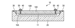
本実施形態による電子部品300は、デバイスユニット10と、支持部材20とを備えている。デバイスユニット10は、対向する第1主面10Aと第2主面10Bとを有する略平板状の構造体であり、半導体ユニットと称することもできる。デバイスユニット10の第1主面10A側には、半導体素子11が設けられている。半導体素子11は、デバイスユニット10の第2主面10B側に設けられていてもよい。支持部材20は、略平板状の構造体であり、一方の主面(図1(b)において上側)に、上部平坦面21と、上部平坦面21に対して窪んだ凹部22とが設けられている。凹部22は、傾斜面SLを有する。凹部22は、一例では、その底を含む底面BTMと、底面BTMに対して傾斜した傾斜面とを含み、底面BTMに向かうほど開口幅が狭くなっている。
The
デバイスユニット10は、図1(b)に示すように、第1主面10Aが支持部材20の凹部22に対向するように、支持部材20に固定されている。デバイスユニット10の第1主面10Aの周縁部は、支持部材20の凹部22の側面である傾斜面SLに接している。より具体的には、デバイスユニット10の第1主面10Aと端面との境界領域(角部(稜部)CR)は、支持部材20の凹部22の傾斜面SLに接している。換言すると、デバイスユニット10の端面は、デバイスユニット10の第1主面10Aに垂直な方向において、支持部材20の凹部22の傾斜面SLに重なっている。凹部22の底面BTMはデバイスユニット10の第1主面10Aに沿っており、凹部22の傾斜面SLは、デバイスユニット10の第1主面10Aに対して傾斜している。なお、デバイスユニット10の端面とは、第1主面10A及び第2主面10Bと交差するデバイスユニット10の側面である。
As shown in FIG. 1 (b), the
凹部22の傾斜面SLは、必ずしも底面BTMに対する傾斜角が一定な平面である必要はなく、例えば底面BTMに渡って連続する曲面形状であってもよい。また、凹部22の側面は、必ずしも1つの平面や曲面で構成される傾斜面SLである必要はなく、複数の面で構成される形状、例えば階段状等であってもよい。ただし、傾斜面SLの形状が凹部22の各側面において異なっているとデバイスユニット10が凹部22に対して斜めに配置される虞があるため、傾斜面SLの形状は凹部22の全側面において同じであることが望ましい。
The inclined surface SL of the
デバイスユニット10の端面と凹部22の傾斜面SLとの間には、樹脂部材30が設けられている。樹脂部材30は、図1(b)に示すように、支持部材20の上部平坦面21に延在して設けられても構わない。デバイスユニット10の第1主面10Aと凹部22の底面BTMとの間には空隙が設けられている。この空隙はデバイスユニット10により塞がれており、デバイスユニット10の第1主面10Aと凹部22の底面BTMとの間に樹脂部材30は漏れ込んではいない。すなわち、樹脂部材30は、デバイスユニット10の第1主面10Aと凹部22の底面BTMとの間に延在していない。
A
次に、デバイスユニット10と支持部材20の凹部22との関係について、図2を用いてより具体的に説明する。なお、図2は、例えば図1(a)のA−A′線に沿った断面図であるが、A−A′線に直行する方向の断面においても以下に説明する関係と同様の関係を有している。
Next, the relationship between the
図2(a)は、幅がXであるデバイスユニット10を、支持部材20の上部平坦面21における開口幅がY1、底面BTMにおける開口幅がY2である凹部22に配置した場合の断面模式図である。この場合、デバイスユニット10の幅Xと、開口幅Y1と、開口幅Y2とは、Y2<X<Y1の関係となる。すなわち、凹部22の開口幅は、底面BTMにおいてデバイスユニット10の幅よりも狭く、底面BTMから離れた部位においてデバイスユニット10の幅よりも広い。換言すると、凹部22の開口幅は、デバイスユニット10の第1主面10Aに対して凹部22の底の側において、デバイスユニット10の幅よりも狭い。また、デバイスユニット10の第1主面10Aに対して凹部22の底とは反対側において、デバイスユニット10の幅よりも広い。凹部22の両側の側面において傾斜面SLの形状が同じとき、デバイスユニット10と凹部22とが中心を揃えて配置されるため、デバイスユニット10の端面と凹部22の上端部との距離Zは、Z=(Y1−X)/2となる。
FIG. 2A is a schematic cross-sectional view when the
図2(b)は、図2(a)の点線で囲んだ部分を拡大した図である。上部平坦面21に対する凹部22の深さをH、傾斜面SLの傾斜角をθ1とすると、デバイスユニット10の第1主面10Aと底面BTMとの間のギャップGは、式(1)のように表される。
G=H−Z×tanθ1=H−(Y1−X)×tanθ1/2 …(1)
FIG. 2B is an enlarged view of the portion surrounded by the dotted line in FIG. 2A. Assuming that the depth of the
G = HZ × tan θ1 = H- (Y1-X) × tan θ1 / 2… (1)
つまり、デバイスユニット10の第1主面10Aと底面BTMとの間のギャップGは、デバイスユニット10の幅Xと、凹部22の開口幅Y1と、傾斜角θ1とによって一律に決定される。したがって、例えば複数の凹部22が設けられた支持部材20の各凹部22にデバイスユニット10を1つずつ配置するような場合においても、デバイスユニット10と凹部22との間のギャップGを均等にすることが可能となる。
That is, the gap G between the first
例えば、傾斜角θ1が60°、凹部22の深さHが100μm、デバイスユニット10の幅Xが10mm、凹部22の開口幅Y1が10.08mmであるとすると、式(1)からギャップGは30.7μmとなる。この場合に、凹部22の加工時の寸法精度により凹部22の開口幅Y1が±1μm変動したとすると、ギャップGは±0.87μm程度変動することとなる。また、傾斜角θ1が+1°変動したとすると(つまり、θ1=61°)、ギャップGは27.84μmとなり、ギャップGの変動量は2.88μmとなる。
For example, assuming that the inclination angle θ1 is 60 °, the depth H of the
デバイスユニット10が固体撮像装置の場合、支持部材20に付着した異物が撮像素子で結像しないように、固体撮像装置と支持部材との間に概ね数十μm程度のギャップGを設けるのが一般的である。したがって、上述した程度のギャップ変動量であれば、固体撮像装置の特性に影響することはない。
When the
デバイスユニット10の第1主面10Aと端面との境界領域(角部CR)は、例えば図2(c)に示すように、デバイスユニット10の第1主面10A及び端面に対して傾斜した傾斜面SL2を設けた面取り構造としてもよい。デバイスユニット10の角部CRを面取りしていない図2(b)に示すような構造の場合、角部CRの頂部に応力が集中し、デバイスユニット10にチッピング等の損傷が生じる可能性がある。境界領域に傾斜面SL2を設けることで、支持部材20との間の接触面積が増加して境界領域に集中する応力を緩和することができ、デバイスユニット10に損傷が生じるのを抑制することができる。この場合、支持部材20の傾斜面SLの傾斜角θ1とデバイスユニット10の傾斜面SL2の傾斜角θ2とは、等しくするのが好ましい。
The boundary region (corner CR) between the first
デバイスユニット10は、特に限定されるものではなく、例えば図3に示すような種々の構造を適用可能である。なお、以下の説明において、各基板の第1主面は、デバイスユニット10の第1主面10A側の面に対応するものとする。また、各基板の第2主面は、デバイスユニット10の第2主面10B側の面に対応するものとする。
The
図3(a)に示すデバイスユニット10は、半導体基板100の第1主面100A側に配された半導体素子11と、半導体基板100の第2主面100B側に配された外部接続端子50とを含む。半導体素子11と外部接続端子50とは、半導体基板100を貫くように設けられた貫通電極40を介して電気的に接続されている。
The
図3(b)に示すデバイスユニット10は、半導体基板100と、半導体基板100を搭載した実装基板101とを含む。半導体基板100の第1主面100A側に半導体素子11が配され、実装基板101の第2主面101B側に外部接続端子50が配されている。半導体素子11と外部接続端子50とは、実装基板101を貫くように設けられた貫通電極40と、ワイヤWとを介して電気的に接続されている。
The
図3(c)に示すデバイスユニット10は、実装基板101と、実装基板101の上に配された半導体基板100とを含む。半導体基板100の第1主面100A側に半導体素子11が配され、実装基板101の第2主面101B側に外部接続端子50が配されている。半導体素子11と外部接続端子50とは、半導体基板100及び実装基板101を貫くように設けられた貫通電極40を介して電気的に接続されている。
The
図3(b)及び図3(c)のように実装基板101を有する構成においては、支持部材20の凹部22の傾斜面SLに設置されるデバイスユニット10の境界領域は、実装基板101の第1主面101Aと端部との間の境界領域であるのが望ましい。
In the configuration having the mounting
ここではデバイスユニット10が単一の基板で構成される場合と2つの基板を積層することにより構成される場合とを例示したが、デバイスユニット10が3つ以上の基板を積層することにより構成される場合にも同様の態様を適用することが可能である。
Here, the case where the
次に、本実施形態による電子部品の製造方法について、図4及び図5を用いて説明する。なお、電子部品の製造には、公知の半導体製造プロセスを用いることができる。また、ここでは説明を省略するが、後述する各工程の間に、必要に応じてその他の工程、例えば熱処理工程や洗浄処理工程等を行ってもよい。 Next, a method of manufacturing an electronic component according to the present embodiment will be described with reference to FIGS. 4 and 5. A known semiconductor manufacturing process can be used for manufacturing electronic components. Further, although the description is omitted here, other steps such as a heat treatment step and a cleaning treatment step may be performed between the steps described later, if necessary.
まず、対向する第1主面100Aと第2主面100Bとを有する半導体基板100を用意する(図4(a))。半導体基板100は、形成しようとする半導体素子11に応じて適宜選択することができる。例えば、半導体基板100には、シリコン基板やGaAs基板等が用いることができる。ここでは、半導体基板100として厚さ725μmのシリコン基板を用いるものとする。
First, a
次いで、半導体基板100の第1主面100A(図4において上側)側に、半導体素子11を形成する(図4(b))。なお、ここでは図示は省略するが、半導体素子11は、トランジスタやダイオードのほか、素子分離膜、配線層、層間絶縁膜等、デバイスユニット10の所定の機能を実現するために必要な構成要素を含む。半導体基板100には複数の半導体素子11が形成され、完成後には各々の半導体素子11の電気特性等の検査が行われる。
Next, the
次いで、複数の半導体素子11が設けられた半導体基板100を、半導体素子11の形成領域毎に個片化し、複数のデバイスユニット10を形成する(図4(c))。半導体基板100の個片化には、ブレードダイシング、レーザーダイシング、プラズマダイシング等の方法を用いることができる。上述のように、ギャップGの精度は寸法加工精度に依存するため、半導体基板100の個片化には寸法加工精度に優れた方法、例えばプラズマダイシングを用いるのが好ましい。
Next, the
また、半導体基板100とは別に、対向する第1主面200Aと第2主面200Bとを有する支持部材200を用意する。支持部材200は、特に限定されるものではないが、例えばガラス基板やシリコン基板等を適用することができる。ここでは、支持部材200として厚さ500μmの石英ガラス基板を用いるものとする。
Further, separately from the
次いで、支持部材200の第1主面200A(図5において上側)の上に、凹部22の形成予定領域に開口部212を有するマスク210を形成する(図5(a))。マスク210には、例えばノボラック系のポジ型フォトレジストを用いることができる。この場合、フォトリソグラフィによってフォトレジスト膜をパターニングすることにより、開口部212を有するマスク210を形成することができる。マスク210は、フォトレジスト膜のパターンを転写したハードマスクでもよい。
Next, a
次いで、マスク210をマスクとして支持部材200をエッチングし、支持部材200の第1主面200A側に、傾斜面SLと底面BTMとを含む凹部22を形成する(図5(b))。凹部22を形成するためのエッチングは、傾斜面SLが形成できる方法であれば特に限定されるものではなく、ウェットエッチングでもドライエッチングでもよい。或いは、ウェットエッチングとドライエッチングとを併用してもよい。処理時間を短縮する観点からは、エッチング速度が速いウェットエッチングが好適である。なお、石英ガラス基板のウェットエッチングには、例えばフッ化水素酸を用いたウェットエッチングを適用可能である。一般的なウェットエッチングは等方的にエッチングが進行するため、マスク210の端部ではサイドエッチングが生じ、凹部22は図5(b)のような傾斜面SLと底面BTMとを有する形状となる。ここでは、凹部22の深さが100μmになるまでウェットエッチングを行うものとする。
Next, the
次いで、凹部22の形成に用いたマスク210を除去する(図5(c))。マスク210をフォトレジストにより形成している場合、TMAH(テトラメチルアンモニウムヒドロキシド)等の有機剥離液を用いたウェット処理やプラズマアッシング処理等によってマスク210を除去することができる。
Next, the
このようにして、支持部材200に、複数の凹部22を形成する。なお、支持部材200の第1主面200Aのうち、凹部22を形成していない部分が、前述の上部平坦面21に相当する。
In this way, a plurality of
次いで、支持部材200に設けられた複数の凹部22に、図4(c)の工程で形成したデバイスユニット10をそれぞれ設置する(図5(d))。デバイスユニット10は、その第1主面10Aが支持部材200の凹部22に対向するように設置する。デバイスユニット10の形成工程で電気特性等の検査を行っている場合、検査に合格したデバイスユニット10のみを支持部材200に設置するのが電子部品の収率を向上する点で好ましい。このとき、デバイスユニット10は支持部材200の凹部22の4つの傾斜面SLで支持された状態となるため、設置後の搬送時にデバイスユニット10の位置ずれや凹部22の外側への飛び出しは抑制される。
Next, the
次いで、支持部材200の第1主面200A側のデバイスユニット10の間の領域にディスペンス法や印刷法などの方法により樹脂部材30を塗布した後、加熱やUV照射等の手段により樹脂部材30を硬化する(図5(e))。これにより、デバイスユニット10を支持部材200に接着・固定する。このとき、デバイスユニット10は凹部22の傾斜面SLに当接しているため、デバイスユニット10の第1主面10Aと支持部材20の凹部22とで囲まれた空間に樹脂部材30が侵入するのを抑制することができる。
Next, the
デバイスユニット10を支持部材200の凹部22に設置した後、大気圧よりも圧力の高い環境に移し、その環境下で樹脂部材30を塗布すると更によい。このようにすることで、デバイスユニット10と支持部材200との間の空間内の気圧よりもデバイスユニット10の第2主面10B側の気圧が高くなり、この気圧差によってデバイスユニット10が支持部材200に押し付けられた状態となる。これにより、デバイスユニット10と凹部22の傾斜面SLとがより確実に当接した状態となる。この状態で樹脂部材30を塗布し硬化することで、樹脂部材30がデバイスユニット10の第1主面10Aと支持部材200の凹部22とで囲まれた空間に侵入するのをさらに抑制することができる。
It is further preferable to install the
デバイスユニット10と凹部22の傾斜面SLとが完全には接しておらず多少の隙間が生じていた場合、毛細管現象によりその隙間から樹脂部材30が浸透することはある。しかしながら、上述した本実施形態の構成を適用することで、デバイスユニット10の第1主面10Aや凹部22の底面BTMにまで樹脂部材30が漏れ込むことは抑制することができる。
When the
なお、ここではデバイスユニット10の間にのみ樹脂部材30を形成したが、デバイスユニット10の第2主面10Bを埋めるように樹脂部材30を全面に形成しても構わない。
Although the
次いで、支持部材200及び樹脂部材30をブレードダイシング等の手段により切断して個片化し、本実施形態による電子部品300を完成する(図5(f))。個片化した後の支持部材200が、図1等における支持部材20である。
Next, the
本実施形態の製造方法を用いることで、デバイスユニット10の第1主面10Aや支持部材20の凹部22の底面BTMに樹脂部材30が漏れ込むのを抑制することができる。これにより、例えばデバイスユニット10が固体撮像装置であり第1主面10A側に光電変換素子が配置される場合にあっては、光電変換素子の有効画素領域を広く配置することが可能となる。
By using the manufacturing method of the present embodiment, it is possible to prevent the
このように、本実施形態によれば、デバイスユニット10の第1主面10Aや支持部材20の凹部22の底面BTMに樹脂部材30が漏れ込むのを抑制することができ、半導体素子11の有効素子領域を拡大することができる。同一の有効素子領域を維持する観点から見れば、樹脂部材30の漏れ込みを抑制できることは、電子部品の小型化が可能であることを意味する。
As described above, according to the present embodiment, it is possible to prevent the
[第2実施形態]
本発明の第2実施形態による電子部品及びその製造方法について、図6及び図7を用いて説明する。図6は、本実施形態による電子部品の構造を示す概略断面図である。図7は、本実施形態による電子部品の製造方法を示す工程断面図である。第1実施形態による電子部品と同様の構成要素には同一の符号を付し、説明を省略し或いは簡潔にする。
[Second Embodiment]
An electronic component and a method for manufacturing the electronic component according to the second embodiment of the present invention will be described with reference to FIGS. 6 and 7. FIG. 6 is a schematic cross-sectional view showing the structure of an electronic component according to the present embodiment. FIG. 7 is a process sectional view showing a method of manufacturing an electronic component according to the present embodiment. The same components as those of the electronic components according to the first embodiment are designated by the same reference numerals, and the description thereof will be omitted or simplified.
本実施形態による電子部品300は、図6に示すように、デバイスユニット10として、図3(a)に示した構造のデバイスユニット10を適用したものである。すなわち、デバイスユニット10の半導体基板100の中には、第1主面10Aから第2主面10Bに渡って貫通電極40が設けられている。そして、第1主面10A側に設けられた半導体素子11と第2主面10B側に設けられた外部接続端子50とが、貫通電極40を介して電気的に接続されている。その他の点は、第1実施形態による電子部品と同様である。
As shown in FIG. 6, the
なお、本実施形態による電子部品において、デバイスユニット10の第2主面10Bが支持部材20の上部平坦面21よりも突出している場合、例えばフリップチップ接続等により、外部接続端子50を回路基板等に直に接続することも可能である。
In the electronic component according to the present embodiment, when the second
次に、本実施形態による電子部品の製造方法について、図7を用いて説明する。
まず、図4(a)乃至図4(c)に示す第1実施形態による電子部品の製造方法と同様にして、デバイスユニット10を形成する。また、図5(a)乃至図5(c)に示す第1実施形態による電子部品の製造方法と同様にして、支持部材200に複数の凹部22を形成する。
Next, a method of manufacturing an electronic component according to the present embodiment will be described with reference to FIG. 7.
First, the
次いで、支持部材200に設けられた複数の凹部22に、第1実施形態による電子部品の製造方法と同様にして、形成したデバイスユニット10をそれぞれ設置する(図7(a))。
Next, the formed
次いで、第1実施形態による電子部品の製造方法と同様にして、少なくともデバイスユニット10の間の領域に樹脂部材30を形成し、支持部材20とデバイスユニット10を接着する(図7(b))。
Next, the
次いで、必要に応じて、デバイスユニット10を第2主面10B側から研磨(バックグラインド)し、デバイスユニット10を薄化する。この際、樹脂部材30もデバイスユニット10とともに研磨されるため、デバイスユニット10の第2主面10Bと樹脂部材30の表面とが略平坦な状態となる(図7(c))。ここでは、デバイスユニット10の厚さが例えば150μmになるまで研磨を行うものとする。なお、デバイスユニット10を薄化することには、貫通電極40の形成が容易になる等の利点がある。
Next, if necessary, the
次いで、デバイスユニット10に、第2主面10Bから第1主面10Aに設けられた配線に達し、半導体素子11に電気的に接続された貫通電極40と、貫通電極40に電気的に接続された外部接続端子50とを形成する(図7(d))。貫通電極40は、半導体基板100に、第1主面10A側に配された不図示の電極部に達する貫通ビア(TSV)を形成した後、この貫通ビアを導電部材で埋めることにより形成することができる。半導体基板100がシリコン基板の場合、貫通ビアの形成には、いわゆるボッシュ法を用いることができる。貫通ビアに埋め込む導電部材としては、銅(Cu)や金(Au)等を用いることができる。これら導電部材の貫通ビアへの埋め込みには、電解メッキ等の方法を適用可能である。外部接続端子50は、例えば、貫通電極40の上にフラックス(不図示)を介して半田ボールを搭載した後、250℃程度の温度で半田ボールをリフローすることにより、形成することができる。
Next, the
次いで、支持部材200及び樹脂部材30をブレードダイシング等の手段により切断して個片化し、本実施形態による電子部品300を完成する(図7(e))。
Next, the
以上のように、デバイスユニット10に貫通電極40を設ける場合でも、本発明の製造方法を用いることができ、デバイスユニット10の第1主面10A及び支持部材200の凹部22の底面BTMに樹脂部材30が延在するのを抑制することができる。これにより、例えばデバイスユニット10が固体撮像装置であり第1主面10A側に光電変換素子が配置される場合にあっては、光電変換素子の有効画素領域を広く配置することが可能となる。
As described above, even when the through
このように、本実施形態によれば、デバイスユニット10に貫通電極40を設ける場合にも、デバイスユニット10の第1主面10Aや支持部材20の凹部22の底面BTMに樹脂部材30が漏れ込むのを抑制することができる。これにより、半導体素子11の有効素子領域を拡大することができる。
As described above, according to the present embodiment, even when the through
[第3実施形態]
本発明の第3実施形態による電子部品及びその製造方法について、図8乃至図10を用いて説明する。図8は、本実施形態による電子部品の構造を示す概略断面図である。図9及び図10は、本実施形態による電子部品の製造方法を示す工程断面図である。第1及び第2実施形態による電子部品と同様の構成要素には同一の符号を付し、説明を省略し或いは簡潔にする。
[Third Embodiment]
An electronic component and a method for manufacturing the electronic component according to the third embodiment of the present invention will be described with reference to FIGS. 8 to 10. FIG. 8 is a schematic cross-sectional view showing the structure of the electronic component according to the present embodiment. 9 and 10 are process cross-sectional views showing a method of manufacturing an electronic component according to the present embodiment. The same components as those of the electronic components according to the first and second embodiments are designated by the same reference numerals, and the description thereof will be omitted or simplified.
はじめに、本実施例による電子部品の構造について、図8を用いて説明する。図8(a)は、本実施形態による電子部品の構造を示す上面図である。図8(b)は、図8(a)のA−A′線に沿った概略断面図である。図8(c)は、図8(b)の点線で囲んだ部分を拡大した図である。 First, the structure of the electronic component according to this embodiment will be described with reference to FIG. FIG. 8A is a top view showing the structure of the electronic component according to the present embodiment. FIG. 8B is a schematic cross-sectional view taken along the line AA'of FIG. 8A. FIG. 8 (c) is an enlarged view of the portion surrounded by the dotted line in FIG. 8 (b).
本実施形態による電子部品300は、デバイスユニット10と支持部材20とを有する点で、第1及び第2実施形態と共通している。一方、本実施形態による電子部品300は、以下の点において第1及び第2実施形態による電子部品とは異なっている。第1の点は、図8(a)及び図8(b)に示すように、支持部材20に、凹部22の傾斜面SLから凹部の外の面(上部平坦面21)に延在し、外部接続端子50に電気的に接続された配線層70(第1の配線層)が設けられていることである。第2の点は、図8(b)に示すように、デバイスユニット10の第1主面10A側の角部CRが面取りされて傾斜面SL2が設けられており、傾斜面SL2の上に半導体素子11に電気的に接続された配線層60(第2の配線層)が配されていることである。配線層60と配線層70とは、傾斜面SLと傾斜面SL2とが対向する部分において、電気的に接続されている。
The
配線層70は、図8(a)に示すように、支持部材20の凹部22の傾斜面SLから支持部材20の上部平坦面21に渡って配置されている。外部接続端子50は、図8(b)に示すように、上部平坦面21上において、樹脂部材30に設けられた開口部を介して配線層70に電気的に接続されている。
As shown in FIG. 8A, the
図8(c)には半導体素子11の一例として、半導体基板100の第1主面100A側に設けられたトランジスタTR、複数層からなる配線層WR、トランジスタTRと配線層WRとの間及び配線層WRと配線層WRとの間に配された絶縁層INSを示している。デバイスユニット10の傾斜面SL2から延在して設けられた配線層60は、絶縁層INSに設けられたビアホールを介して、配線層WRに電気的に接続されている。
FIG. 8C shows, as an example of the
デバイスユニット10を支持部材20の凹部22に配置することで、配線層60と配線層70とが当接し電気的に接続される。さらに、支持部材20に配された配線層70によって外部接続端子50と配線層60とが電気的に接続され、その結果、外部接続端子50と半導体素子11とが電気的に接続される。
By arranging the
以上の構造とすることで、第2実施形態の場合のような貫通電極40を設けることなく、外部電源(不図示)を、外部接続端子50、配線層70及び配線層60を介して半導体素子11に電気的に接続することが可能となる。また、第1及び第2実施形態の場合と同様、デバイスユニット10の第1主面10A及び支持部材200の凹部22の底面BTMに樹脂部材30が延在するのを抑制することができる。これにより、例えばデバイスユニット10が固体撮像装置であり第1主面10A側に光電変換素子が配置される場合にあっては、光電変換素子の有効画素領域を広く配置することが可能となる。
With the above structure, the external power supply (not shown) is connected to the semiconductor element via the
次に、本実施形態による電子部品の製造方法について、図9及び図10を用いて説明する。 Next, a method of manufacturing an electronic component according to the present embodiment will be described with reference to FIGS. 9 and 10.
まず、図4(a)及び図4(b)に示す第1実施形態による電子部品の製造方法と同様にして、半導体基板100の第1主面100A側に、半導体素子11を形成する(図9(a))。なお、後工程で半導体基板100を個片化する際に割断する領域(ダイシング領域)に半導体素子11を構成する絶縁膜や配線層等が配置されている場合は、これらをエッチング等の手段により除去し、第1主面100A側に半導体基板100を露出させる。
First, the
次いで、半導体基板100の第1主面100A側のダイシング領域に、傾斜面SL2と底面BTM2とからなる溝80を形成する(図9(b))。具体的には、半導体基板100の第1主面100Aにフォトレジスト膜(不図示)を形成後、フォトリソグラフィにより、半導体素子11間のダイシング領域を露出するようにフォトレジスト膜をパターニングする。次いで、パターニングしたフォトレジスト膜をマスクとして半導体基板100をエッチングし、溝80を形成する。ここでは、例えばプロセスガスとしてSF6を用いたプラズマエッチングにより、例えば傾斜面SL2の傾斜角θ2が64°で深さが30μmの溝80を形成するものとする。
Next, a
次いで、半導体素子11から溝80の傾斜面SL2に延在する配線層60を形成する(図9(c))。この際、溝80の領域内のダイシング領域の配線層60を除去しておくことで、ダイシングブレードの目詰まりや、ダイシング時に配線層60に損傷が及ぶことを抑制することができる。なお、図示は省略するが、半導体基板100と配線層60との間には、酸化シリコン等の絶縁膜が形成される。配線層60の構成材料には、アルミニウムや銅のような金属材料や、ITOやIZOなどの酸化物導電体のような導電性材料であれば、任意の材料を用いることができる。ここでは、アルミニウムを主体とする導電性材料により配線層60を形成するものとする。
Next, a
次いで、複数の半導体素子11が設けられた半導体基板100を、例えばプラズマダイシングにより半導体素子11の形成領域毎に個片化し、複数のデバイスユニット10を形成する(図9(d))。プラズマダイシングは、配線層60に損傷が及ぶことなく半導体基板100を個片化できるため好適である。具体的には、半導体基板100の第1主面100Aにフォトレジスト膜(不図示)を形成後、フォトリソグラフィにより、溝80の底面BTM2のみを露出するようにフォトレジスト膜をパターニングする。次いで、パターニングしたフォトレジスト膜をマスクとして半導体基板100をエッチングし、半導体基板100を個片化する。例えば、半導体基板100がシリコン基板の場合には、いわゆるボッシュ法を用いて半導体基板100を垂直方向に加工し、半導体基板100を個片化する。
Next, the
また、デバイスユニット10の製造とは別に、図5(a)乃至図5(c)に示す第1実施形態による電子部品の製造方法と同様にして、複数の凹部22が設けられた支持部材200を形成する(図10(a))。
Further, apart from the manufacture of the
次いで、支持部材200の第1主面200A側に、上部平坦面21から凹部22の傾斜面SLに延在する配線層70を形成する(図10(b))。配線層70の構成材料には、アルミニウムや銅などの金属材料や、ITOやIZOなどの酸化物導電物など、導電性を有する材料を用いることができる。例えば、支持部材200の第1主面200A上の全面にアルミニウム膜を堆積後、このアルミニウム膜をフォトリソグラフィ及びドライエッチングを用いてパターニングすることにより、配線層70を形成する。
Next, a
次いで、支持部材200に設けられた複数の凹部22に、第1実施形態による電子部品の製造方法と同様にして、形成したデバイスユニット10をそれぞれ設置する(図10(c))。これにより、デバイスユニット10に設けられた配線層60と支持部材200に設けられた配線層70とが当接した状態となる。
Next, the formed
次いで、第1実施形態による電子部品の製造方法と同様にして、少なくともデバイスユニット10の間の領域に樹脂部材30を形成し、支持部材20とデバイスユニット10を接着する。次いで、樹脂部材30に、上部平坦面21上の配線層70を露出する開口部32を形成する(図10(d))。樹脂部材30は、第1実施形態と同様の方法で塗布することができる。樹脂部材30には、感光性樹脂材料を適用可能である。ここでは、樹脂部材30として感光性ポリイミドを用い、フォトリソグラフィにより樹脂部材30をパターニングし、開口部32を形成するものとする。
Next, the
なお、樹脂部材30の形成後、開口部32の形成前に、第2実施形態の場合と同様にして、デバイスユニット10を第2主面10B側からバックグラインドし、デバイスユニット10を薄化してもよい。
After the
次いで、樹脂部材30の開口部32に、配線層70に電気的に接続された外部接続端子50を形成する(図10(e))。外部接続端子50は、例えば、開口部32にフラックス(不図示)を介して半田ボールを搭載した後、250℃程度の温度で半田ボールをリフローすることにより、形成することができる。
Next, an
なお、本実施形態では、上部平坦面21の配線層70上に外部接続端子50を設けたが、開口部32とデバイスユニット10の第2主面10Bとを繋ぐ別の配線を設け、デバイスユニット10の第2主面10B上に外部接続端子50を設けてもよい。
In the present embodiment, the
次いで、支持部材200及び樹脂部材30をブレードダイシング等の手段により切断して個片化し、本実施形態による電子部品300を完成する(図10(f))。個片化した後の支持部材200が、図8等における支持部材20である。
Next, the
以上のように、本実施形態の電子部品では、貫通電極を形成することなく外部電源と半導体素子11とを電気的に接続することが可能である。また、本実施形態の電子部品では、デバイスユニット10の角部CRに傾斜面SL2を設けているため、支持部材20の凹部22の傾斜面SLとの接触部におけるチッピング等の損傷を抑制することができる。また、デバイスユニット10と支持部材20との間の接触面における隙間も生じにくいため、樹脂部材30の浸入をより抑制することができる。これにより、例えばデバイスユニット10が固体撮像装置であり第1主面10A側に光電変換素子が配置される場合にあっては、光電変換素子の有効画素領域を広く配置することが可能となる。
As described above, in the electronic component of the present embodiment, it is possible to electrically connect the external power supply and the
このように、本実施形態によれば、デバイスユニット10に貫通電極を設けることなく、デバイスユニット10と支持部材20とを容易に電気的に接続することができる。また、デバイスユニット10にチッピング等の不良が生じるのを抑制することができる。また、第1及び第2実施形態と同様、半導体素子11の有効素子領域を拡大することができる。
As described above, according to the present embodiment, the
[変形実施形態]
本発明は、上記実施形態に限らず種々の変形が可能である。
[Modification Embodiment]
The present invention is not limited to the above embodiment and can be modified in various ways.
例えば、いずれかの実施形態の一部の構成を他の実施形態に追加した例や、他の実施形態の一部の構成と置換した例も、本発明の実施形態である。例えば、上記第3実施形態による電子部品において、第2実施形態と同様の貫通電極40を更に設けるようにしてもよい。
For example, an example in which a partial configuration of any of the embodiments is added to another embodiment or an example in which a partial configuration of another embodiment is replaced with another embodiment is also an embodiment of the present invention. For example, in the electronic component according to the third embodiment, the same through
また、上記実施形態では、半導体素子11の一例として固体撮像素子を例示したが、デバイスユニット10が有する半導体素子11は、固体撮像素子に限定されるものではない。
Further, in the above embodiment, the solid-state image pickup device is exemplified as an example of the
また、上記実施形態で説明した電子部品を実装した回路部品は、種々の電子機器に適用可能である。電子機器は、特に限定されるものではなく、例えば、デジタルスチルカメラ、ビデオカメラ、スマートフォン、パーソナルコンピュータ、家電製品(IoT)等を例示することができる。 Further, the circuit component on which the electronic component described in the above embodiment is mounted can be applied to various electronic devices. The electronic device is not particularly limited, and examples thereof include a digital still camera, a video camera, a smartphone, a personal computer, and a home electric appliance (IoT).
また、上記実施形態で説明した電子部品は、移動装置を備えた輸送機器に適用することも可能である。例えば、輸送機器は、上記実施形態で説明した電子部品から出力された信号に基づいて移動装置を制御する制御装置を備えることができる。移動装置は、特に限定されるものではなく、例えば、エンジン、モータ、車輪、プロペラ等の動力源や推進機構を例示することができる。輸送機器は、特に限定されるものではなく、例えば、飛行機、車両、船舶等を例示することができる。 Further, the electronic component described in the above embodiment can also be applied to a transportation device provided with a mobile device. For example, the transport device can include a control device that controls the mobile device based on the signal output from the electronic component described in the above embodiment. The moving device is not particularly limited, and examples thereof include a power source such as an engine, a motor, wheels, and a propeller, and a propulsion mechanism. The transportation equipment is not particularly limited, and examples thereof include airplanes, vehicles, and ships.
また、本明細書中の各用語は、本発明を説明する目的で用いられたものに過ぎず、その均等物をも含み得、本発明は、その用語の厳密な意味に限定されるものでない。 In addition, each term in the present specification is used only for the purpose of explaining the present invention, and may include an equivalent thereof, and the present invention is not limited to the strict meaning of the term. ..
上記実施形態は、何れも本発明を実施するにあたっての具体化の例を示したものに過ぎず、これらによって本発明の技術的範囲が限定的に解釈されてはならないものである。すなわち、本発明はその技術思想、又はその主要な特徴から逸脱することなく、様々な形で実施することができる。 All of the above embodiments are merely examples of embodiment of the present invention, and the technical scope of the present invention should not be construed in a limited manner by these. That is, the present invention can be implemented in various forms without departing from the technical idea or its main features.
BTM…底面
CR…角部
SL,SL2…傾斜面
10…デバイスユニット
11…半導体素子
100…半導体基板
101…実装基板
20,200…支持部材
21…支持部材における上部平坦面
22…支持部材における凹部
30…樹脂部材
40…貫通電極
50…外部接続端子
60,70…配線層
300…電子部品
BTM ... Bottom surface CR ... Corner SL, SL2 ...
Claims (19)
基板を有し、前記基板の主面が前記凹部に対向するように前記支持部材に固定されたデバイスユニットと、を備え、
前記凹部の開口幅は、前記主面に対して前記凹部の底の側において前記デバイスユニットの幅よりも狭く、前記主面に対して前記凹部の底とは反対側において前記デバイスユニットの前記幅よりも広く、
前記基板の前記主面に垂直な方向において、前記基板の端面が前記凹部の前記側面に重なっており、
前記基板の前記主面には光電変換素子が配置されている
ことを特徴とする電子部品。 A support member provided with a recess having a bottom surface and a side surface,
A device unit having a substrate and fixed to the support member so that the main surface of the substrate faces the recess.
The opening width of the recess is narrower than the width of the device unit on the bottom side of the recess with respect to the main surface, and the width of the device unit on the side opposite to the bottom of the recess with respect to the main surface. Wider than
The end face of the substrate overlaps the side surface of the recess in a direction perpendicular to the main surface of the substrate.
An electronic component characterized in that a photoelectric conversion element is arranged on the main surface of the substrate.
ことを特徴とする請求項1記載の電子部品。 The side surface has an inclined surface inclined with respect to the main surface of the substrate, the bottom surface is along the main surface, the inclined surface is inclined with respect to the bottom surface, and the main surface of the substrate is used. The electronic component according to claim 1, wherein the end surface of the substrate overlaps the inclined surface of the recess in a direction perpendicular to the surface.
ことを特徴とする請求項2記載の電子部品。 The electronic component according to claim 2, wherein the boundary region between the main surface and the end surface of the device unit is in contact with the inclined surface of the recess.
ことを特徴とする請求項3記載の電子部品。 The electronic component according to claim 3, wherein the boundary region is inclined with respect to the main surface and the end surface.
前記デバイスユニットは、前記デバイスユニットのうちの前記主面と前記端面の境界領域に配された第2の配線層を有し、
前記側面の上において前記第1の配線層と前記第2の配線層とが電気的に接続されている
ことを特徴とする請求項1乃至4のいずれか1項に記載の電子部品。 The support member has a first wiring layer provided on the side surface of the recess.
The device unit has a second wiring layer arranged in a boundary region between the main surface and the end surface of the device unit.
The electronic component according to any one of claims 1 to 4, wherein the first wiring layer and the second wiring layer are electrically connected on the side surface.
ことを特徴とする請求項5記載の電子部品。 The electronic component according to claim 5, wherein the first wiring layer extends to an outer surface of the recess of the support member.
ことを特徴とする請求項1乃至6のいずれか1項に記載の電子部品。 The electronic component according to any one of claims 1 to 6, wherein the device unit has an external connection terminal on the side opposite to the recess.
ことを特徴とする請求項1乃至7のいずれか1項に記載の電子部品。 The device unit includes a semiconductor substrate and a mounting substrate on which the semiconductor substrate is mounted, and according to any one of claims 1 to 7, the mounting substrate has a main surface and an end surface. Electronic components.
ことを特徴とする請求項1乃至8のいずれか1項に記載の電子部品。 The electronic component according to any one of claims 1 to 8, wherein the recess is closed by the device unit.
ことを特徴とする請求項1乃至9のいずれか1項に記載の電子部品。 The electronic component according to any one of claims 1 to 9, wherein the device unit protrudes from the support member on the side opposite to the main surface.
基板を有し、前記基板の主面が前記凹部の前記底面に沿うように前記支持部材に固定されたデバイスユニットと、
前記デバイスユニットの端面と前記凹部の前記側面との間に設けられた樹脂部材と、を備え、
前記凹部の開口幅は、前記主面に対して前記凹部の底の側において前記デバイスユニットの幅よりも狭く、前記主面に対して前記凹部の底とは反対側において前記デバイスユニットの前記幅よりも広く、
前記デバイスユニットと前記凹部の前記底面との間に空隙が設けられており、
前記樹脂部材は、前記デバイスユニットの前記主面と前記底面との間に延在していない
ことを特徴とする電子部品。 A support member provided with a recess having a bottom surface and a side surface,
A device unit having a substrate and fixed to the support member so that the main surface of the substrate is along the bottom surface of the recess.
A resin member provided between the end surface of the device unit and the side surface of the recess is provided.
The opening width of the recess is narrower than the width of the device unit on the bottom side of the recess with respect to the main surface, and the width of the device unit on the side opposite to the bottom of the recess with respect to the main surface. Wider than
A gap is provided between the device unit and the bottom surface of the recess.
The resin member is an electronic component that does not extend between the main surface and the bottom surface of the device unit.
ことを特徴とする請求項11記載の電子部品。 11. The electronic component according to claim 11, wherein the boundary region between the main surface and the end surface of the device unit is in contact with the side surface of the recess.
ことを特徴とする請求項12記載の電子部品。 12. The electronic component according to claim 12, wherein the boundary region is inclined with respect to the main surface and the end surface.
前記デバイスユニットは、前記デバイスユニットのうちの前記主面と前記端面の境界領域に配された第2の配線層を有し、
前記側面の上において前記第1の配線層と前記第2の配線層とが電気的に接続されている
ことを特徴とする請求項11乃至13のいずれか1項に記載の電子部品。 The support member has a first wiring layer provided on the side surface of the recess.
The device unit has a second wiring layer arranged in a boundary region between the main surface and the end surface of the device unit.
The electronic component according to any one of claims 11 to 13, wherein the first wiring layer and the second wiring layer are electrically connected on the side surface.
ことを特徴とする請求項14記載の電子部品。 The electronic component according to claim 14, wherein the first wiring layer extends to an outer surface of the recess of the support member.
ことを特徴とする請求項11乃至15のいずれか1項に記載の電子部品。 The electronic component according to any one of claims 11 to 15, wherein the device unit has an external connection terminal on the side opposite to the recess.
ことを特徴とする請求項11乃至16のいずれか1項に記載の電子部品。 The device unit includes a semiconductor substrate and a mounting substrate on which the semiconductor substrate is mounted, and according to any one of claims 11 to 16, the mounting substrate has a main surface and an end surface. Electronic components.
ことを特徴とする請求項11乃至17のいずれか1項に記載の電子部品。 The electronic component according to any one of claims 11 to 17, wherein the device unit protrudes from the support member on the side opposite to the main surface.
前記電子部品が実装された回路部品と
を備えることを特徴とする機器。 The electronic component according to any one of claims 1 to 18.
A device including a circuit component on which the electronic component is mounted.
Priority Applications (3)
| Application Number | Priority Date | Filing Date | Title |
|---|---|---|---|
| JP2017044645A JP6968553B2 (en) | 2017-03-09 | 2017-03-09 | Electronic components and their manufacturing methods |
| US15/910,882 US10367102B2 (en) | 2017-03-09 | 2018-03-02 | Electronic component and equipment |
| CN201810192411.3A CN108573988B (en) | 2017-03-09 | 2018-03-09 | Electronic component and equipment |
Applications Claiming Priority (1)
| Application Number | Priority Date | Filing Date | Title |
|---|---|---|---|
| JP2017044645A JP6968553B2 (en) | 2017-03-09 | 2017-03-09 | Electronic components and their manufacturing methods |
Publications (3)
| Publication Number | Publication Date |
|---|---|
| JP2018148155A JP2018148155A (en) | 2018-09-20 |
| JP2018148155A5 JP2018148155A5 (en) | 2020-04-16 |
| JP6968553B2 true JP6968553B2 (en) | 2021-11-17 |
Family
ID=63445588
Family Applications (1)
| Application Number | Title | Priority Date | Filing Date |
|---|---|---|---|
| JP2017044645A Active JP6968553B2 (en) | 2017-03-09 | 2017-03-09 | Electronic components and their manufacturing methods |
Country Status (3)
| Country | Link |
|---|---|
| US (1) | US10367102B2 (en) |
| JP (1) | JP6968553B2 (en) |
| CN (1) | CN108573988B (en) |
Family Cites Families (22)
| Publication number | Priority date | Publication date | Assignee | Title |
|---|---|---|---|---|
| US5093708A (en) * | 1990-08-20 | 1992-03-03 | Grumman Aerospace Corporation | Multilayer integrated circuit module |
| US5986334A (en) | 1996-10-04 | 1999-11-16 | Anam Industrial Co., Ltd. | Semiconductor package having light, thin, simple and compact structure |
| KR101078621B1 (en) | 2003-07-03 | 2011-11-01 | 테쎄라 테크놀로지스 아일랜드 리미티드 | Method and apparatus for packaging integrated circuit devices |
| JP2005116943A (en) * | 2003-10-10 | 2005-04-28 | Seiko Epson Corp | Printed-circuit board, packaging substrate module, manufacturing method for printed-circuit board, and electro-optical devices and electronic apparatuses using same |
| JP4331033B2 (en) * | 2004-03-29 | 2009-09-16 | 浜松ホトニクス株式会社 | Semiconductor light detecting element and manufacturing method thereof |
| JP2006128625A (en) | 2004-09-30 | 2006-05-18 | Oki Electric Ind Co Ltd | Semiconductor device and its manufacturing method |
| EP1961696B1 (en) * | 2005-11-16 | 2013-09-04 | Kyocera Corporation | Electronic device using electronic part sealing board and method of fabricating same |
| US7919410B2 (en) * | 2007-03-14 | 2011-04-05 | Aptina Imaging Corporation | Packaging methods for imager devices |
| JP2009141092A (en) * | 2007-12-06 | 2009-06-25 | Taiyo Yuden Co Ltd | Circuit device provided with semiconductor device and method of manufacturing semiconductor device |
| JP2010166004A (en) * | 2009-01-19 | 2010-07-29 | Panasonic Corp | Semiconductor device and manufacturing method thereof |
| JP2010238995A (en) * | 2009-03-31 | 2010-10-21 | Sanyo Electric Co Ltd | Semiconductor module and camera module mounted with the same |
| JP5694670B2 (en) | 2010-02-05 | 2015-04-01 | キヤノン株式会社 | Solid-state imaging device and manufacturing method thereof |
| US8558392B2 (en) * | 2010-05-14 | 2013-10-15 | Stats Chippac, Ltd. | Semiconductor device and method of forming interconnect structure and mounting semiconductor die in recessed encapsulant |
| JP5877291B2 (en) | 2010-05-14 | 2016-03-08 | パナソニックIpマネジメント株式会社 | Semiconductor device and manufacturing method thereof |
| JP2012182309A (en) * | 2011-03-01 | 2012-09-20 | Seiko Instruments Inc | Optical device |
| JP5709165B2 (en) | 2011-03-10 | 2015-04-30 | セイコーインスツル株式会社 | Optical device |
| JP6164879B2 (en) | 2013-03-08 | 2017-07-19 | セイコーインスツル株式会社 | Package, piezoelectric vibrator, oscillator, electronic equipment and radio clock |
| JP2015002414A (en) | 2013-06-14 | 2015-01-05 | セイコーインスツル株式会社 | Electronic device |
| JP6554338B2 (en) | 2014-07-28 | 2019-07-31 | ローム株式会社 | Semiconductor device |
| JP6373678B2 (en) * | 2014-07-28 | 2018-08-15 | ローム株式会社 | Semiconductor device |
| JP6425933B2 (en) | 2014-07-28 | 2018-11-21 | ローム株式会社 | Semiconductor device |
| JP2016100554A (en) | 2014-11-26 | 2016-05-30 | ローム株式会社 | Semiconductor device |
-
2017
- 2017-03-09 JP JP2017044645A patent/JP6968553B2/en active Active
-
2018
- 2018-03-02 US US15/910,882 patent/US10367102B2/en active Active
- 2018-03-09 CN CN201810192411.3A patent/CN108573988B/en active Active
Also Published As
| Publication number | Publication date |
|---|---|
| CN108573988B (en) | 2023-05-09 |
| JP2018148155A (en) | 2018-09-20 |
| US20180261701A1 (en) | 2018-09-13 |
| US10367102B2 (en) | 2019-07-30 |
| CN108573988A (en) | 2018-09-25 |
Similar Documents
| Publication | Publication Date | Title |
|---|---|---|
| JP6315859B2 (en) | Imaging device, semiconductor device, and imaging unit | |
| JP5183708B2 (en) | Semiconductor device and manufacturing method thereof | |
| JP4139803B2 (en) | Manufacturing method of semiconductor device | |
| US9230939B2 (en) | Method for producing image pickup apparatus, method for producing semiconductor apparatus, and joined wafer | |
| US9231018B2 (en) | Wafer level packaging structure for image sensors and wafer level packaging method for image sensors | |
| US20090050996A1 (en) | Electronic device wafer level scale packages and fabrication methods thereof | |
| US9601531B2 (en) | Wafer-level packaging structure for image sensors with packaging cover dike structures corresponding to scribe line regions | |
| TWI539538B (en) | Semiconductor device and manufacturing method thereof | |
| WO2013103136A1 (en) | Semiconductor device and method for manufacturing same | |
| JP2009194396A (en) | Semiconductor package and method of manufacturing the same | |
| US20090050995A1 (en) | Electronic device wafer level scale packges and fabrication methods thereof | |
| US9362134B2 (en) | Chip package and fabrication method thereof | |
| JP2020077855A (en) | Chip package and manufacturing method thereof | |
| US20170330871A1 (en) | Chip package and manufacturing method thereof | |
| JP6968553B2 (en) | Electronic components and their manufacturing methods | |
| JP4248355B2 (en) | Semiconductor device and manufacturing method of semiconductor device | |
| JP2009295859A (en) | Semiconductor apparatus and method for manufacturing semiconductor apparatus | |
| US8304288B2 (en) | Methods of packaging semiconductor devices including bridge patterns | |
| TW201537734A (en) | Manufacturing method of semiconductor structure | |
| JP7273153B2 (en) | Semiconductor device with through-substrate via and method for manufacturing semiconductor device with through-substrate via | |
| US20200090953A1 (en) | Method of manufacturing semiconductor device | |
| JP5414965B2 (en) | Optical semiconductor device and manufacturing method thereof | |
| JP2010010303A (en) | Semiconductor device | |
| JP2010147355A (en) | Method of manufacturing semiconductor device |
Legal Events
| Date | Code | Title | Description |
|---|---|---|---|
| RD05 | Notification of revocation of power of attorney |
Free format text: JAPANESE INTERMEDIATE CODE: A7425 Effective date: 20171214 |
|
| RD04 | Notification of resignation of power of attorney |
Free format text: JAPANESE INTERMEDIATE CODE: A7424 Effective date: 20180126 |
|
| A521 | Request for written amendment filed |
Free format text: JAPANESE INTERMEDIATE CODE: A523 Effective date: 20200303 |
|
| A621 | Written request for application examination |
Free format text: JAPANESE INTERMEDIATE CODE: A621 Effective date: 20200303 |
|
| A977 | Report on retrieval |
Free format text: JAPANESE INTERMEDIATE CODE: A971007 Effective date: 20210204 |
|
| A131 | Notification of reasons for refusal |
Free format text: JAPANESE INTERMEDIATE CODE: A131 Effective date: 20210209 |
|
| A521 | Request for written amendment filed |
Free format text: JAPANESE INTERMEDIATE CODE: A523 Effective date: 20210409 |
|
| TRDD | Decision of grant or rejection written | ||
| A01 | Written decision to grant a patent or to grant a registration (utility model) |
Free format text: JAPANESE INTERMEDIATE CODE: A01 Effective date: 20210928 |
|
| A61 | First payment of annual fees (during grant procedure) |
Free format text: JAPANESE INTERMEDIATE CODE: A61 Effective date: 20211027 |
|
| R151 | Written notification of patent or utility model registration |
Ref document number: 6968553 Country of ref document: JP Free format text: JAPANESE INTERMEDIATE CODE: R151 |