JP6959863B2 - Collimator for use in substrate processing chamber - Google Patents
Collimator for use in substrate processing chamber Download PDFInfo
- Publication number
- JP6959863B2 JP6959863B2 JP2017527875A JP2017527875A JP6959863B2 JP 6959863 B2 JP6959863 B2 JP 6959863B2 JP 2017527875 A JP2017527875 A JP 2017527875A JP 2017527875 A JP2017527875 A JP 2017527875A JP 6959863 B2 JP6959863 B2 JP 6959863B2
- Authority
- JP
- Japan
- Prior art keywords
- openings
- collimator
- aspect ratio
- substrate
- collimator according
- Prior art date
- Legal status (The legal status is an assumption and is not a legal conclusion. Google has not performed a legal analysis and makes no representation as to the accuracy of the status listed.)
- Active
Links
- 239000000758 substrate Substances 0.000 title claims description 56
- 230000002093 peripheral effect Effects 0.000 claims description 19
- 230000007704 transition Effects 0.000 claims description 16
- 238000005477 sputtering target Methods 0.000 claims description 6
- 239000000463 material Substances 0.000 description 20
- 150000002500 ions Chemical class 0.000 description 12
- 238000004544 sputter deposition Methods 0.000 description 12
- 238000000034 method Methods 0.000 description 11
- 230000008569 process Effects 0.000 description 10
- 238000000151 deposition Methods 0.000 description 8
- 230000008021 deposition Effects 0.000 description 8
- 238000005240 physical vapour deposition Methods 0.000 description 8
- 239000002245 particle Substances 0.000 description 7
- 239000010410 layer Substances 0.000 description 5
- 230000004907 flux Effects 0.000 description 4
- RYGMFSIKBFXOCR-UHFFFAOYSA-N Copper Chemical compound [Cu] RYGMFSIKBFXOCR-UHFFFAOYSA-N 0.000 description 3
- 229910052782 aluminium Inorganic materials 0.000 description 3
- XAGFODPZIPBFFR-UHFFFAOYSA-N aluminium Chemical compound [Al] XAGFODPZIPBFFR-UHFFFAOYSA-N 0.000 description 3
- 229910052802 copper Inorganic materials 0.000 description 3
- 239000010949 copper Substances 0.000 description 3
- 239000004065 semiconductor Substances 0.000 description 3
- 238000001816 cooling Methods 0.000 description 2
- 230000007423 decrease Effects 0.000 description 2
- 238000005516 engineering process Methods 0.000 description 2
- 230000010354 integration Effects 0.000 description 2
- 238000004519 manufacturing process Methods 0.000 description 2
- 229910052751 metal Inorganic materials 0.000 description 2
- 239000002184 metal Substances 0.000 description 2
- 230000009467 reduction Effects 0.000 description 2
- 239000010935 stainless steel Substances 0.000 description 2
- 229910001220 stainless steel Inorganic materials 0.000 description 2
- 208000000659 Autoimmune lymphoproliferative syndrome Diseases 0.000 description 1
- 229910000881 Cu alloy Inorganic materials 0.000 description 1
- 239000011324 bead Substances 0.000 description 1
- 230000008901 benefit Effects 0.000 description 1
- 230000015572 biosynthetic process Effects 0.000 description 1
- 238000005137 deposition process Methods 0.000 description 1
- 239000003989 dielectric material Substances 0.000 description 1
- 230000005684 electric field Effects 0.000 description 1
- 229940082150 encore Drugs 0.000 description 1
- 238000001914 filtration Methods 0.000 description 1
- 238000004377 microelectronic Methods 0.000 description 1
- 239000000203 mixture Substances 0.000 description 1
- 230000007935 neutral effect Effects 0.000 description 1
- 239000002344 surface layer Substances 0.000 description 1
- 239000013077 target material Substances 0.000 description 1
- 238000003466 welding Methods 0.000 description 1
Images


Classifications
-
- C—CHEMISTRY; METALLURGY
- C23—COATING METALLIC MATERIAL; COATING MATERIAL WITH METALLIC MATERIAL; CHEMICAL SURFACE TREATMENT; DIFFUSION TREATMENT OF METALLIC MATERIAL; COATING BY VACUUM EVAPORATION, BY SPUTTERING, BY ION IMPLANTATION OR BY CHEMICAL VAPOUR DEPOSITION, IN GENERAL; INHIBITING CORROSION OF METALLIC MATERIAL OR INCRUSTATION IN GENERAL
- C23C—COATING METALLIC MATERIAL; COATING MATERIAL WITH METALLIC MATERIAL; SURFACE TREATMENT OF METALLIC MATERIAL BY DIFFUSION INTO THE SURFACE, BY CHEMICAL CONVERSION OR SUBSTITUTION; COATING BY VACUUM EVAPORATION, BY SPUTTERING, BY ION IMPLANTATION OR BY CHEMICAL VAPOUR DEPOSITION, IN GENERAL
- C23C14/00—Coating by vacuum evaporation, by sputtering or by ion implantation of the coating forming material
- C23C14/04—Coating on selected surface areas, e.g. using masks
- C23C14/046—Coating cavities or hollow spaces, e.g. interior of tubes; Infiltration of porous substrates
-
- C—CHEMISTRY; METALLURGY
- C23—COATING METALLIC MATERIAL; COATING MATERIAL WITH METALLIC MATERIAL; CHEMICAL SURFACE TREATMENT; DIFFUSION TREATMENT OF METALLIC MATERIAL; COATING BY VACUUM EVAPORATION, BY SPUTTERING, BY ION IMPLANTATION OR BY CHEMICAL VAPOUR DEPOSITION, IN GENERAL; INHIBITING CORROSION OF METALLIC MATERIAL OR INCRUSTATION IN GENERAL
- C23C—COATING METALLIC MATERIAL; COATING MATERIAL WITH METALLIC MATERIAL; SURFACE TREATMENT OF METALLIC MATERIAL BY DIFFUSION INTO THE SURFACE, BY CHEMICAL CONVERSION OR SUBSTITUTION; COATING BY VACUUM EVAPORATION, BY SPUTTERING, BY ION IMPLANTATION OR BY CHEMICAL VAPOUR DEPOSITION, IN GENERAL
- C23C14/00—Coating by vacuum evaporation, by sputtering or by ion implantation of the coating forming material
- C23C14/22—Coating by vacuum evaporation, by sputtering or by ion implantation of the coating forming material characterised by the process of coating
- C23C14/34—Sputtering
- C23C14/35—Sputtering by application of a magnetic field, e.g. magnetron sputtering
-
- H—ELECTRICITY
- H01—ELECTRIC ELEMENTS
- H01J—ELECTRIC DISCHARGE TUBES OR DISCHARGE LAMPS
- H01J37/00—Discharge tubes with provision for introducing objects or material to be exposed to the discharge, e.g. for the purpose of examination or processing thereof
- H01J37/32—Gas-filled discharge tubes
- H01J37/34—Gas-filled discharge tubes operating with cathodic sputtering
- H01J37/3402—Gas-filled discharge tubes operating with cathodic sputtering using supplementary magnetic fields
- H01J37/3405—Magnetron sputtering
- H01J37/3408—Planar magnetron sputtering
-
- H—ELECTRICITY
- H01—ELECTRIC ELEMENTS
- H01J—ELECTRIC DISCHARGE TUBES OR DISCHARGE LAMPS
- H01J37/00—Discharge tubes with provision for introducing objects or material to be exposed to the discharge, e.g. for the purpose of examination or processing thereof
- H01J37/32—Gas-filled discharge tubes
- H01J37/34—Gas-filled discharge tubes operating with cathodic sputtering
- H01J37/3411—Constructional aspects of the reactor
- H01J37/3447—Collimators, shutters, apertures
Description
本開示の実施形態は、一般に半導体製造システムで使用される基板処理チャンバに関する。 Embodiments of the present disclosure relate to substrate processing chambers commonly used in semiconductor manufacturing systems.
サブミクロン以下の特徴を確実に生産することは、次世代の半導体デバイスの超大規模集積(VLSI)および超々大規模集積(ULSI)にとって技術的な課題である。しかしながら、回路技術の小型化が続くとともに、VLSIおよびULSI技術の相互接続部の寸法の縮小は、処理能力にさらなる要求を突きつけてきた。例えば、回路密度が次世代デバイスに向けて増加するとともに、ビアホール、トレンチ、コンタクトなどの相互接続部、ゲート構造および他の特徴、ならびにそれらの間にある誘電体材料の幅が減少し、一方で誘電体層の厚さは、実質的に一定のままであり、結果として特徴のアスペクト比が増加する。
物理的気相堆積(PVD)としても知られているスパッタリングは、集積回路の金属特徴を形成する一般的に用いられる方法である。スパッタリングは、材料層を基板に堆積させる。ターゲットなどのソース材料は、電界によって強く加速されたイオンによって衝撃が与えられる。その衝撃によって、ターゲットから材料が放出され、次いでその材料が基板上に堆積する。堆積中に、放出された粒子は、基板表面に略垂直ではなく、様々な方向に進み、したがって、結果として基板の高アスペクト比の特徴のコーナにオーバーハング構造が形成されることがある。オーバーハングは、望ましくないことには、堆積させた材料内部に孔またはボイドが形成されることがあり、結果として、形成された特徴の導電率が減少する。幾何学形状のアスペクト比が高くなるほど、ボイドなしに充填する困難さの度合いがより高くなる。
Reliably producing submicron features is a technical challenge for ultra-large scale integration (VLSI) and ultra-ultra-large scale integration (ULSI) of next-generation semiconductor devices. However, as circuit technology continues to be miniaturized, the reduction in dimensions of interconnects of VLSI and ULSI technologies has placed further demands on processing power. For example, as circuit densities increase towards next-generation devices, interconnects such as via holes, trenches, contacts, gate structures and other features, and the width of the dielectric material between them decrease, while The thickness of the dielectric layer remains substantially constant, resulting in an increase in the aspect ratio of the feature.
Sputtering, also known as Physical Vapor Deposition (PVD), is a commonly used method of forming metallic features of integrated circuits. Sputtering deposits a layer of material on a substrate. Source materials such as targets are impacted by ions that are strongly accelerated by an electric field. The impact releases the material from the target and then deposits the material on the substrate. During deposition, the emitted particles travel in various directions rather than substantially perpendicular to the substrate surface, thus resulting in the formation of overhang structures at the corners of the substrate's high aspect ratio features. Overhangs can, undesirably, form holes or voids inside the deposited material, resulting in reduced conductivity of the formed features. The higher the aspect ratio of the geometry, the greater the difficulty of filling without voids.
基板表面に達するイオン分画またはイオン密度を特定の範囲に制御することによって、金属層堆積プロセス中に底部および側壁のカバレージを改善する(およびオーバーハングの問題を低減する)ことができる。一例において、ターゲットから追い出された粒子は、特徴内への粒子の軌跡がより垂直となるのを容易に実現するために、コリメータなどのプロセスツールによって制御されることがある。コリメータは、コリメータの通路に衝撃を与え、張り付く、非垂直に進む粒子をフィルタ除去するために、ターゲットと基板との間に比較的長い、一直線の、狭い通路を備える。
所与のコリメータによって達成される実際のフィルタリング量は、少なくとも一部はコリメータを貫通する開孔のアスペクト比に依存する。そのため、基板に垂直に近い経路を進む粒子がコリメータを通過し、基板に堆積し、これによって高アスペクト比の特徴の底部のカバレッジを改善する。しかしながら、典型的には全体的に六角形の形状を有する従来技術のコリメータの使用に関してある問題が存在する。残念ながら、従来技術コリメータを有するPVDチャンバでは、六角形のコリメータのコーナのシャドーイングにより基板のエッジの近くに6点の堆積が残る。
したがって、本発明者は、改善された堆積均一性を有する改善された装置の実施形態を提供した。
By controlling the ion fraction or ion density reaching the substrate surface to a specific range, bottom and side wall coverage can be improved (and overhanging problems are reduced) during the metal layer deposition process. In one example, the particles expelled from the target may be controlled by a process tool such as a collimator to facilitate the trajectory of the particles into the feature to be more vertical. The collimator provides a relatively long, straight, narrow passage between the target and the substrate to filter out particles that impact and stick to the passage of the collimator and travel non-vertically.
The actual amount of filtering achieved by a given collimator depends, at least in part, on the aspect ratio of the openings that penetrate the collimator. As such, particles traveling in a path close to perpendicular to the substrate pass through the collimator and deposit on the substrate, thereby improving bottom coverage of high aspect ratio features. However, there are certain problems with the use of prior art collimators, which typically have an overall hexagonal shape. Unfortunately, in PVD chambers with prior art collimators, shadowing of the corners of the hexagonal collimator leaves six deposits near the edges of the substrate.
Therefore, the inventor has provided an embodiment of an improved device with improved deposition uniformity.
基板処理チャンバで使用するコリメータの実施形態が本明細書で提供される。一部の実施形態では、コリメータは、中心領域、周辺領域、および中心領域と周辺領域との間に配置された遷移領域を有する本体と、第1のアスペクト比を有する中心領域の第1の複数の開孔と、第1のアスペクト比よりも小さい第2のアスペクト比を有する周辺領域の第2の複数の開孔と、遷移領域の第3の複数の開孔であって、遷移領域が中心領域を取り囲む円錐形を形成するように切削されている、第3の複数の開孔と、を含む。 Embodiments of a collimator used in a substrate processing chamber are provided herein. In some embodiments, the collimator is a body having a central region, a peripheral region, and a transition region located between the central region and the peripheral region, and a first plurality of central regions having a first aspect ratio. A second plurality of openings in the peripheral region having a second aspect ratio smaller than the first aspect ratio, and a third plurality of openings in the transition region, the transition region being the center. Includes a third plurality of openings, which are cut to form a conical shape surrounding the region.
一部の実施形態では、基板処理チャンバで使用するためのコリメータは、中心領域、周辺領域、および中心領域と周辺領域との間に配置された遷移領域を有する本体と、第1のアスペクト比を有する中心領域の第1の複数の開孔と、第1のアスペクト比よりも小さい第2のアスペクト比を有する周辺領域の第2の複数の開孔と、遷移領域の第3の複数の開孔であって、遷移領域が中心領域を取り囲む円錐形を形成するように切削されている、第3の複数の開孔と、を含み、第1の複数の開孔、第2の複数の開孔、および第3の複数の開孔がテクスチャ加工され、第1の複数の開孔、第2の複数の開孔、および第3の複数の開孔の上方部分がチャンファーを含む。
一部の実施形態では、プロセスチャンバは、内部容積を画成するチャンバ本体と、内部容積の上方部分に配置されたスパッタリングターゲットと、スパッタリングターゲットの下に配置された基板支持体と、スパッタリングターゲットと基板支持体との間の内部容積に配置されたコリメータとを含み、コリメータが、中心領域、周辺領域、および中心領域と周辺領域との間に配置された遷移領域を有する本体、第1のアスペクト比を有する中心領域の第1の複数の開孔、第1のアスペクト比よりも小さい第2のアスペクト比を有する周辺領域の第2の複数の開孔、ならびに遷移領域の第3の複数の開孔であって、遷移領域が中心領域を取り囲む円錐形を形成するように切削されている、第3の複数の開孔を含む。
In some embodiments, the collimator for use in the substrate processing chamber has a first aspect ratio with a body having a central region, a peripheral region, and a transition region located between the central region and the peripheral region. A first plurality of openings in the central region, a second plurality of openings in the peripheral region having a second aspect ratio smaller than the first aspect ratio, and a third plurality of openings in the transition region. A first plurality of openings, a second plurality of openings, including a third plurality of openings, wherein the transition region is cut to form a conical shape surrounding the central region. , And the third plurality of openings are textured, and the first plurality of openings, the second plurality of openings, and the upper portion of the third plurality of openings include a chamber.
In some embodiments, the process chamber comprises a chamber body that defines the internal volume, a sputtering target located above the internal volume, a substrate support located below the sputtering target, and a sputtering target. A body in which the collimeter has a central region, a peripheral region, and a transition region disposed between the central region and the peripheral region, including a collimeter arranged in an internal volume between the substrate support and the first aspect. A first plurality of openings in the central region having a ratio, a second plurality of openings in a peripheral region having a second aspect ratio smaller than the first aspect ratio, and a third plurality of openings in the transition region. Includes a third plurality of openings that are holes that are cut so that the transition region forms a cone that surrounds the central region.
本開示の他のおよびさらなる実施形態が以下に記載される。
上で簡単に要約され、以下でより詳細に論じる本開示の実施形態は、添付図面に表される本開示の例示的な実施形態を参照することによって理解され得る。しかしながら、添付図面は、本開示の典型的な実施形態のみを示し、したがって、範囲を限定していると考えられるべきではなく、その理由は本開示が他の等しく効果的な実施形態を受け入れることができるためである。
Other and further embodiments of the present disclosure are described below.
The embodiments of the present disclosure briefly summarized above and discussed in more detail below can be understood by reference to the exemplary embodiments of the present disclosure set forth in the accompanying drawings. However, the accompanying drawings show only typical embodiments of the present disclosure and should therefore not be considered limiting in scope, because the disclosure accepts other equally effective embodiments. This is because it can be done.
理解を容易にするために、可能な場合は同一の参照数字を使用して、各図に共通の同一の要素を指定した。図は、縮尺通りには描かれておらず、明瞭にするために簡略化されることがある。一部の実施形態の要素および特徴は、さらに詳説することなく他の実施形態において有益に組み込まれることがある。
半導体基板のマイクロ電子デバイスの製造に使用されるようなコリメータの実施形態が本明細書で提供される。本明細書に開示されるようなコリメータは、有利には処理される基板全体にわたって堆積の均一性を改善する。
本開示の実施形態は、本明細書では物理的気相堆積(PVD)チャンバに関して例示として記載される。しかしながら、本発明のコリメータは、一般に、非垂直に進む粒子をフィルタするためにいかなる基板処理チャンバでも使用され得る。図1は、本開示の実施形態による、材料をスパッタ堆積させるのに適した、内部にコリメータ110が配置された処理チャンバ100(例えば、PVDチャンバ)を示す。本開示から恩恵を得るように構成されてもよい適切なPVDチャンバの説明に役立つ例は、ALPS(登録商標)PlusおよびSIP ENCORE(登録商標)PVD処理チャンバを含み、両方ともカリフォルニアのサンタクララのApplied Materials,Inc.から市販されている。Applied Materials,Inc.ならびに他のメーカーから市販されている他の処理チャンバも、本明細書に記載された実施形態により適合させることができる。
For ease of understanding, the same reference numbers are used where possible to specify the same elements that are common to each figure. The figures are not drawn to scale and may be simplified for clarity. The elements and features of some embodiments may be beneficially incorporated in other embodiments without further elaboration.
Embodiments of a collimator such as those used in the manufacture of microelectronic devices on semiconductor substrates are provided herein. Collimators as disclosed herein advantageously improve deposition uniformity throughout the substrate being processed.
The embodiments of the present disclosure are described herein by way of example with respect to a physical vapor deposition (PVD) chamber. However, the collimators of the present invention can generally be used in any substrate processing chamber to filter particles traveling non-vertically. FIG. 1 shows a processing chamber 100 (eg, PVD chamber) with a
チャンバ100は、内部容積106を画成するチャンバ本体105を有する。チャンバ本体105は、接地されたチャンバ壁150、および接地されたチャンバ壁150の上に配置された、接地された導電性アダプタ144を含む。一部の実施形態では、処理チャンバ100は、下部シールド180、上部シールド186、およびコリメータ110を有するプロセスキット140を含む。また、処理チャンバ100は、スパッタリング面145を有するターゲット142などのスパッタリング源、および基板154を受けるための、周辺エッジ153を有する基板支持体152を含む。基板支持体152は、接地されたチャンバ壁150内部に配置されてもよい。
The
ターゲット142は、誘電体アイソレータ146を介して、接地された導電性アダプタ144によって支持されている。ターゲット142は、スパッタリング中に基板154の表面に堆積させる材料を含み、基板154に形成される高アスペクト比の特徴にシード層として堆積させるための銅を含むことができる。本明細書で使用されるように、用語アスペクト比は、要素の幅に対する要素の高さ、長さ、または深さの比を指す。一部の実施形態では、ターゲット142は、銅などのスパッタ可能な材料の金属表面層とアルミニウムなどの構造材料のバッキング層との結合組成物も含むことができる。
一部の実施形態では、基板支持体152は、スパッタ被覆される高アスペクト比の特徴を有する基板154を支持し、この特徴の底部がターゲット142の主表面に平面対向している。基板支持体152は、ターゲット142のスパッタリング面と略平行に配置された平面の基板受取り面を有する。基板支持体152は、基板154を処理チャンバ100の下方部分のロードロックバルブ(図示せず)を通って基板支持体152上に移送することができるように、底部チャンバ壁160に接続されたベローズ158によって垂直に移動可能であってもよい。その場合、基板支持体は、図示されるような堆積位置へ持ち上げられてもよい。
The
In some embodiments, the
一部の実施形態では、処理ガスは、質量流量制御装置164によってガス源162から処理チャンバ100の下方部分内へ供給されてもよい。処理チャンバ100に結合された制御可能な直流(DC)電源148を使用して、ターゲット142に負電圧またはバイアスを印加することができる。基板154上にDC自己バイアスを誘起するために、高周波(RF)電源156が基板支持体152に結合されてもよい。一部の実施形態では、基板支持体152は、接地されてもよい。一部の実施形態では、基板支持体152は、代わりに電気的に浮遊状態であってもよい。
In some embodiments, the processing gas may be supplied by the mass
一部の実施形態では、マグネトロン170は、ターゲット142の上に配置されている。マグネトロン170は、シャフト176に接続されたベースプレート174によって支持された複数の磁石172を含むことができ、このシャフト176は、軸方向に処理チャンバ100および基板154の中心軸と位置合わせされてもよい。磁石172は、プラズマを発生させて、それにより著しいイオンフラックスがターゲット142を打つよう、ターゲット142の正面近くの処理チャンバ100内部で磁場を生成し、ターゲット材料のスパッタ放出を引き起こす。ターゲット142の表面全体にわたって磁場の均一性を向上させるために、磁石172をシャフト176の回りで回転させてもよい。
一部の実施形態では、処理チャンバ100は、チャンバ壁150によって支持された、チャンバ壁150と電気的に結合された支持体フランジ182を有する接地された下部シールド180を含んでもよい。上部シールド186は、導電性アダプタ144のフランジ184によって支持され、フランジ184に電気的に結合されている。上部シールド186および下部シールド180は、導電性アダプタ144およびチャンバ壁150がそうであるように、電気的に結合されている。一部の実施形態では、上部シールド186および下部シールド180は、両方ともステンレス鋼で構成されている。一部の実施形態では、処理チャンバ100は、上部シールド186に結合された中間のシールド(図示せず)を含んでもよい。一部の実施形態では、上部シールド186および下部シールド180は、処理チャンバ100内部で電気的に浮遊状態であってもよい。一部の実施形態では、上部シールド186および下部シールド180は、代わりに電源に結合されてもよい。
In some embodiments, the
In some embodiments, the
一部の実施形態では、上部シールド186は、上部シールド186とターゲット142との間の狭い間隙188によってターゲット142の環状の側面凹部にぴったりと嵌合する上方部分を有してもよく、この間隙188は、プラズマが侵入して、誘電体アイソレータ146をスパッタ被覆するのを防ぐのに十分に狭い。また、上部シールド186は、下向きに突き出る先端部190を含んでもよく、この先端部190は、スパッタ堆積材料による下部シールド180と上部シールド186との結合を防ぐために、下部シールド180と上部シールド186との間の接触面をカバーする。
In some embodiments, the
一部の実施形態では、下部シールド180は、円筒状の外バンド196内へと下方に延在してもよく、この外バンド196は、全体にチャンバ壁150に沿って基板支持体152の上面よりも下に延在する。下部シールド180は、円筒状の外バンド196から放射状に内向きに延在するベースプレート198を有することができる。ベースプレート198は、基板支持体152の周辺を取り囲む、上向きに延在する円筒状の内バンド103を含んでもよい。一部の実施形態では、カバーリング102は、基板支持体152が下方の装荷位置にある場合は、円筒状の内バンド103の頂部に載り、基板支持体が上方の堆積位置にある場合は、基板支持体152の外周部に載り、基板支持体152をスパッタ堆積から保護する。
下部シールド180は、基板支持体152に面するターゲット142のスパッタリング面145を取り巻き、基板支持体152の外周壁も取り巻く。また、下部シールド180は、下部シールド180の背後の構成要素および表面上への、ターゲット142のスパッタリング面145に由来するスパッタ堆積物の堆積を低減させるために処理チャンバ100のチャンバ壁150をカバーし、陰にする。例えば、下部シールド180は、基板支持体152の表面、基板154の部分、チャンバ壁150、および処理チャンバ100の底部壁160を保護することができる。
In some embodiments, the
The
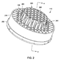
一部の実施形態では、コリメータ110をターゲット142と基板支持体152との間に配置することによって指向性のスパッタリングを実現することができる。コリメータ110は、機械的に、および電気的に上部シールド186に結合されてもよい。一部の実施形態では、コリメータ110は、処理チャンバ100の下方に配置された中間のシールド(図示せず)に結合されてもよい。一部の実施形態では、コリメータ110は、上部シールド186に一体化されていてもよい。一部の実施形態では、コリメータ110は、上部シールド186に溶接されている。一部の実施形態では、コリメータ110は、処理チャンバ100内部で電気的に浮遊状態であってもよい。一部の実施形態では、コリメータ110は、電源に結合されていてもよい。コリメータ110は、チャンバ内部のガスおよび/または材料のフラックスを導くために複数の開孔128を含む。一部の実施形態では、図2〜図4に示されるように、開孔128は、六角形の形状を有してもよい。
In some embodiments, directional sputtering can be achieved by placing the
図2は、本開示の一部の実施形態によるコリメータ110の等角図である。図3は、図1の処理チャンバ100に配置することができるコリメータ110の平面図である。一部の実施形態では、コリメータ110は、最密配置で開孔128を分離する壁126を有する略ハニカム構造を有する。開孔128のアスペクト比は、開孔128の幅129で割った開孔128の深さ(特定位置でコリメータの長さに等しい)として規定されてもよい。一部の実施形態では、壁126の厚さは、約0.06インチ〜約0.18インチの間である。一部の実施形態では、壁126の厚さは、約0.12インチ〜約0.15インチの間である。一部の実施形態では、開孔128のそれぞれに外接する円305の直径は、1.5インチであってもよい。一部の実施形態では、コリメータ110は、アルミニウム、銅、およびステンレス鋼から選択された材料で構成されている。
FIG. 2 is an isometric view of the
コリメータ110のハニカム構造は、コリメータ110を通過するイオンの流路、イオン分画、およびイオン軌道の挙動を最適化するために、一体型フラックスオプティマイザー310として働くことができる。一部の実施形態では、シールド部分202に隣接する壁126は、チャンファー350および半径を有する。コリメータ110のシールド部分202は、処理チャンバ100にコリメータ110を設置するのに役立つ。
一部の実施形態では、コリメータ110は、単一のアルミニウムの塊から機械加工されてもよい。コリメータ110は、被覆され、または陽極酸化されてもよい。あるいは、コリメータ110は、処理環境と両立可能な他の材料から作られてもよく、1つまたは複数の部分品で構成されてもよい。あるいは、シールド部分202および一体型フラックスオプティマイザー310は、別々の部片として形成され、溶接などの適切な取り付け手段を使用して互いに結合される。一部の実施形態では、コリメータ110の壁126は、高応力膜(例えば、銅合金)の壁126への接着を改善するためにテクスチャ加工(例えば、ビーズブラスト)されてもよい。
The honeycomb structure of the
In some embodiments, the
一部の実施形態では、コリメータ110は、コリメータ110を通過するイオンの方向を制御するようにバイポーラモードで電気的にバイアスされてもよい。例えば、コリメータ110をバイアスするようにコリメータ110に交互するパルス状の正または負の電圧を提供するために、制御可能な直流(DC)またはACコリメータ電源(電源390)がコリメータ110に結合されてもよい。一部の実施形態では、電源390は、DC電源である。
コリメータ110は、基板154に対して垂直に近い、所定の角度を上回る角度でターゲット142の材料から放出されたイオンおよび中性粒子をトラップするために、フィルタとして機能する。コリメータ118の開孔128は、ターゲット142の材料の中心領域または周辺領域から放出されたイオンが異なる割合でコリメータ110を通過することができるように、コリメータ110の幅全体にわたってアスペクト比が変化してもよい。その結果、基板154の周辺領域ならびに中心領域に堆積するイオンの数およびイオンの到来角が両方とも調整され制御される。したがって、基板154の表面全体にわたって材料をより均一にスパッタ堆積させることができる。さらに、高アスペクト比の特徴、特に基板154の周辺部近くに位置する高アスペクト比のビアホールならびにトレンチの底部および側壁に材料をより均一に堆積させることができる。
In some embodiments, the
The
図4は、図2に示されるコリメータ110の断面図である。コリメータ110は、約2.5:1〜約3.3:1などの高アスペクト比を有する第1の複数の開孔を有する中心領域220を有する本体218を含む。一部の実施形態では、中心領域の第1の複数の開孔は、約3.3:1のアスペクト比を有する。コリメータ110の第2の複数の開孔のアスペクト比は、周辺領域240において減少する。一部の実施形態では、周辺領域240の第2の複数の開孔は、約1:1のアスペクト比を有する。アスペクト比が高くなるほど、コリメータ110の中心領域220の開孔をより多くすることができる。一部の実施形態では、例えば、中心領域220は、61個の開孔を含む。
FIG. 4 is a cross-sectional view of the
一部の実施形態では、コリメータ110の半径方向の開孔の減少は、中心領域220と周辺領域240との間に配置された遷移領域260を設けることによって達成される。第3の複数の開孔は、遷移領域260が第1の複数の開孔を取り囲む円錐形を形成するように所定の角度に沿って切削されている。一部の実施形態では、所定の角度は、15°〜45°の間であってもよい。遷移領域は、有利には中心領域220で円形プロファイル280の開孔を備え、これによって、従来の六角形のコリメータのコーナによって引き起こされるシャドーイングによる基板154のエッジ近くの6点堆積を克服する。
In some embodiments, the reduction of radial openings in the
開孔128の壁126の上方部分は、開孔128がスパッタされた材料によってふさがれる割合を減少させるためにチャンファー406を有する。チャンファー406は、開孔128内へ所定の距離402延在し、所定の角度404で形成されている。一部の実施形態では、所定の距離402は、約0.15インチ〜約1インチの間であり、所定の角度は、約2.5°〜約15°の間である。一部の実施形態では、所定の距離402および所定の角度404は、それぞれ約0.15インチおよび15°である。一部の実施形態では、所定の距離402および所定の角度404は、それぞれ約1インチおよび2.5°である。
The upper portion of the
したがって、冷却プロセスツールアダプタおよびこれを用いるプロセスチャンバの実施形態が本明細書で開示された。冷却プロセスツールアダプタは、有利にはプロセスチャンバのプロセスツールを支持し、一方で使用中に生成されるプロセスツールからの熱を除去するのを容易にする。 Therefore, embodiments of cooling process tool adapters and process chambers using them are disclosed herein. The cooling process tool adapter favorably supports the process tool in the process chamber, while facilitating the removal of heat from the process tool generated during use.
前述の事項は、本開示の実施形態を対象としているが、本開示の他のおよびさらなる実施形態が本開示の基本的な範囲から逸脱せずに考案されてもよい。 Although the above-mentioned matters are intended for the embodiments of the present disclosure, other and further embodiments of the present disclosure may be devised without departing from the basic scope of the present disclosure.
Claims (15)
第1のアスペクト比を有する前記中心領域の第1の複数の開孔と、
前記第1のアスペクト比よりも小さい第2のアスペクト比を有する前記周辺領域の第2の複数の開孔と、
前記遷移領域の第3の複数の開孔であって、前記遷移領域が前記中心領域を取り囲む円錐形を形成するように切削されている、第3の複数の開孔と、
を備え、
前記中心領域は、前記遷移領域によって形成される円形のエッジを有する、基板処理チャンバで使用するためのコリメータ。 A body having a central region, a peripheral region, and a transition region arranged between the central region and the peripheral region,
With the first plurality of openings in the central region having the first aspect ratio,
A second plurality of openings in the peripheral region having a second aspect ratio smaller than the first aspect ratio, and
A third plurality of openings in the transition region, wherein the transition region is cut to form a conical shape surrounding the central region.
With
The central region is a collimator for use in a substrate processing chamber having a circular edge formed by the transition region.
前記内部容積の上方部分に配置されたスパッタリングターゲットと、
前記スパッタリングターゲットの下に配置された基板支持体と、
前記スパッタリングターゲットと前記基板支持体との間の前記内部容積に配置されたコリメータであって、請求項1から14までのいずれか1項に記載される、コリメータと、
を備える、基板処理チャンバ。 The chamber body that defines the internal volume and
With the sputtering target placed in the upper part of the internal volume,
A substrate support placed under the sputtering target and
Wherein a collimator that is disposed on the interior volume between the sputtering target and the substrate support, Ru as claimed in any one of claims 1 to 14, and the collimator,
A substrate processing chamber.
Applications Claiming Priority (5)
| Application Number | Priority Date | Filing Date | Title |
|---|---|---|---|
| US201462085009P | 2014-11-26 | 2014-11-26 | |
| US62/085,009 | 2014-11-26 | ||
| US14/607,273 US9543126B2 (en) | 2014-11-26 | 2015-01-28 | Collimator for use in substrate processing chambers |
| US14/607,273 | 2015-01-28 | ||
| PCT/US2015/061826 WO2016085805A1 (en) | 2014-11-26 | 2015-11-20 | Collimator for use in substrate processing chambers |
Publications (3)
| Publication Number | Publication Date |
|---|---|
| JP2017537227A JP2017537227A (en) | 2017-12-14 |
| JP2017537227A5 JP2017537227A5 (en) | 2019-01-10 |
| JP6959863B2 true JP6959863B2 (en) | 2021-11-05 |
Family
ID=56009603
Family Applications (1)
| Application Number | Title | Priority Date | Filing Date |
|---|---|---|---|
| JP2017527875A Active JP6959863B2 (en) | 2014-11-26 | 2015-11-20 | Collimator for use in substrate processing chamber |
Country Status (9)
| Country | Link |
|---|---|
| US (1) | US9543126B2 (en) |
| EP (2) | EP3723113A1 (en) |
| JP (1) | JP6959863B2 (en) |
| KR (1) | KR101824517B1 (en) |
| CN (2) | CN107002220B (en) |
| IL (1) | IL251944B (en) |
| SG (2) | SG11201703543RA (en) |
| TW (1) | TWI618172B (en) |
| WO (1) | WO2016085805A1 (en) |
Families Citing this family (19)
| Publication number | Priority date | Publication date | Assignee | Title |
|---|---|---|---|---|
| KR20180063347A (en) | 2015-10-27 | 2018-06-11 | 어플라이드 머티어리얼스, 인코포레이티드 | Bias-capable flux optimizer / collimator for PVD sputter chambers |
| US11037768B2 (en) | 2016-03-05 | 2021-06-15 | Applied Materials, Inc. | Methods and apparatus for controlling ion fraction in physical vapor deposition processes |
| KR102534091B1 (en) * | 2016-11-18 | 2023-05-17 | 어플라이드 머티어리얼스, 인코포레이티드 | Collimators for use in physical vapor deposition chambers |
| JP2018154880A (en) * | 2017-03-17 | 2018-10-04 | 株式会社東芝 | Collimator and processing device |
| CN109390222B (en) * | 2017-08-08 | 2021-01-05 | 宁波江丰电子材料股份有限公司 | Collimator gauge and using method thereof |
| USD858468S1 (en) | 2018-03-16 | 2019-09-03 | Applied Materials, Inc. | Collimator for a physical vapor deposition chamber |
| USD859333S1 (en) | 2018-03-16 | 2019-09-10 | Applied Materials, Inc. | Collimator for a physical vapor deposition chamber |
| US11017989B2 (en) | 2018-03-16 | 2021-05-25 | Samsung Electronics Co., Ltd. | Collimator, fabrication apparatus including the same, and method of fabricating a semiconductor device using the same |
| WO2020088415A1 (en) * | 2018-10-31 | 2020-05-07 | 北京北方华创微电子装备有限公司 | Reaction chamber and semiconductor processing device |
| CN109457231B (en) * | 2018-11-26 | 2020-04-03 | 武汉华星光电半导体显示技术有限公司 | Evaporation carrier plate and method for evaporating substrate by using same |
| CN111826607A (en) * | 2019-04-18 | 2020-10-27 | 天通(嘉兴)新材料有限公司 | Laser tube cap coating shielding jig |
| CN110643958A (en) * | 2019-10-21 | 2020-01-03 | 吴浪生 | Physical coating equipment for realizing wafer by sputtering |
| USD937329S1 (en) | 2020-03-23 | 2021-11-30 | Applied Materials, Inc. | Sputter target for a physical vapor deposition chamber |
| USD998575S1 (en) | 2020-04-07 | 2023-09-12 | Applied Materials, Inc. | Collimator for use in a physical vapor deposition (PVD) chamber |
| US11635338B2 (en) * | 2020-10-23 | 2023-04-25 | Applied Materials, Inc. | Rapid chamber vacuum leak check hardware and maintenance routine |
| USD1009816S1 (en) | 2021-08-29 | 2024-01-02 | Applied Materials, Inc. | Collimator for a physical vapor deposition chamber |
| USD997111S1 (en) | 2021-12-15 | 2023-08-29 | Applied Materials, Inc. | Collimator for use in a physical vapor deposition (PVD) chamber |
| FI20225334A1 (en) * | 2022-04-21 | 2023-10-22 | Biomensio Ltd | Collimator for Production of Piezoelectric Layers with Tilted c-Axis Orientation |
| USD1024149S1 (en) * | 2022-12-16 | 2024-04-23 | Applied Materials, Inc. | Collimator for a physical vapor deposition (PVD) chamber |
Family Cites Families (16)
| Publication number | Priority date | Publication date | Assignee | Title |
|---|---|---|---|---|
| US5223108A (en) * | 1991-12-30 | 1993-06-29 | Materials Research Corporation | Extended lifetime collimator |
| JPH06295903A (en) * | 1993-02-09 | 1994-10-21 | Matsushita Electron Corp | Sputtering device |
| KR970009828B1 (en) * | 1994-02-23 | 1997-06-18 | Sansung Electronics Co Ltd | Fabrication method of collimator |
| JPH08260139A (en) * | 1995-03-23 | 1996-10-08 | Sony Corp | Collimator for film formation, film forming device and production of electronic device |
| US5650052A (en) * | 1995-10-04 | 1997-07-22 | Edelstein; Sergio | Variable cell size collimator |
| US6362097B1 (en) | 1998-07-14 | 2002-03-26 | Applied Komatsu Technlology, Inc. | Collimated sputtering of semiconductor and other films |
| JP2005504885A (en) | 2001-07-25 | 2005-02-17 | アプライド マテリアルズ インコーポレイテッド | Barrier formation using a novel sputter deposition method |
| US20030029715A1 (en) | 2001-07-25 | 2003-02-13 | Applied Materials, Inc. | An Apparatus For Annealing Substrates In Physical Vapor Deposition Systems |
| WO2005041172A1 (en) * | 2003-09-29 | 2005-05-06 | Seagate Technology Llc | System, method and collimator for oblique deposition |
| JP2007273490A (en) * | 2004-03-30 | 2007-10-18 | Renesas Technology Corp | Method of manufacturing semiconductor integrated circuit device |
| EP1710324B1 (en) | 2005-04-08 | 2008-12-03 | STMicroelectronics S.r.l. | PVD process and chamber for the pulsed deposition of a chalcogenide material layer of a phase change memory device |
| US9316413B2 (en) | 2008-06-11 | 2016-04-19 | Honeywell International Inc. | Selectable efficiency versus comfort for modulating furnace |
| CN102066603B (en) * | 2008-06-17 | 2013-04-10 | 应用材料公司 | Apparatus and method for uniform deposition |
| US20090308739A1 (en) | 2008-06-17 | 2009-12-17 | Applied Materials, Inc. | Wafer processing deposition shielding components |
| KR102020010B1 (en) * | 2009-04-24 | 2019-09-09 | 어플라이드 머티어리얼스, 인코포레이티드 | Wafer processing deposition shielding components |
| CN103343317A (en) * | 2013-07-11 | 2013-10-09 | 南京大学 | Preparation method of TiO2 nanoparticle antireflective film based on nanocluster beam deposition system |
-
2015
- 2015-01-28 US US14/607,273 patent/US9543126B2/en active Active
- 2015-11-20 WO PCT/US2015/061826 patent/WO2016085805A1/en active Application Filing
- 2015-11-20 EP EP20172767.4A patent/EP3723113A1/en not_active Withdrawn
- 2015-11-20 EP EP15862359.5A patent/EP3140851B1/en active Active
- 2015-11-20 CN CN201580061359.2A patent/CN107002220B/en active Active
- 2015-11-20 KR KR1020167031655A patent/KR101824517B1/en active IP Right Grant
- 2015-11-20 SG SG11201703543RA patent/SG11201703543RA/en unknown
- 2015-11-20 CN CN201811129929.9A patent/CN109338293B/en active Active
- 2015-11-20 SG SG10202009604WA patent/SG10202009604WA/en unknown
- 2015-11-20 JP JP2017527875A patent/JP6959863B2/en active Active
- 2015-11-20 TW TW104138508A patent/TWI618172B/en active
-
2017
- 2017-04-26 IL IL251944A patent/IL251944B/en active IP Right Grant
Also Published As
| Publication number | Publication date |
|---|---|
| US9543126B2 (en) | 2017-01-10 |
| IL251944B (en) | 2021-06-30 |
| WO2016085805A1 (en) | 2016-06-02 |
| EP3140851A1 (en) | 2017-03-15 |
| US20160145735A1 (en) | 2016-05-26 |
| EP3140851A4 (en) | 2017-11-01 |
| CN107002220A (en) | 2017-08-01 |
| EP3723113A1 (en) | 2020-10-14 |
| CN109338293A (en) | 2019-02-15 |
| IL251944A0 (en) | 2017-06-29 |
| EP3140851B1 (en) | 2020-05-06 |
| CN109338293B (en) | 2021-06-04 |
| CN107002220B (en) | 2020-04-17 |
| TW201622045A (en) | 2016-06-16 |
| TWI618172B (en) | 2018-03-11 |
| JP2017537227A (en) | 2017-12-14 |
| KR20160138306A (en) | 2016-12-02 |
| SG10202009604WA (en) | 2020-11-27 |
| KR101824517B1 (en) | 2018-02-01 |
| SG11201703543RA (en) | 2017-06-29 |
Similar Documents
| Publication | Publication Date | Title |
|---|---|---|
| JP6959863B2 (en) | Collimator for use in substrate processing chamber | |
| TWI761889B (en) | Biasable flux optimizer/collimator for pvd sputter chamber | |
| KR20190097315A (en) | Apparatus and method for uniform deposition | |
| TWI839710B (en) | Biasable flux optimizer/collimator for pvd sputter chamber |
Legal Events
| Date | Code | Title | Description |
|---|---|---|---|
| A521 | Request for written amendment filed |
Free format text: JAPANESE INTERMEDIATE CODE: A523 Effective date: 20181120 |
|
| A621 | Written request for application examination |
Free format text: JAPANESE INTERMEDIATE CODE: A621 Effective date: 20181120 |
|
| A977 | Report on retrieval |
Free format text: JAPANESE INTERMEDIATE CODE: A971007 Effective date: 20190920 |
|
| A131 | Notification of reasons for refusal |
Free format text: JAPANESE INTERMEDIATE CODE: A131 Effective date: 20191007 |
|
| A601 | Written request for extension of time |
Free format text: JAPANESE INTERMEDIATE CODE: A601 Effective date: 20200107 |
|
| A601 | Written request for extension of time |
Free format text: JAPANESE INTERMEDIATE CODE: A601 Effective date: 20200309 |
|
| A521 | Request for written amendment filed |
Free format text: JAPANESE INTERMEDIATE CODE: A523 Effective date: 20200407 |
|
| A131 | Notification of reasons for refusal |
Free format text: JAPANESE INTERMEDIATE CODE: A131 Effective date: 20200923 |
|
| A601 | Written request for extension of time |
Free format text: JAPANESE INTERMEDIATE CODE: A601 Effective date: 20201222 |
|
| A131 | Notification of reasons for refusal |
Free format text: JAPANESE INTERMEDIATE CODE: A131 Effective date: 20210527 |
|
| A521 | Request for written amendment filed |
Free format text: JAPANESE INTERMEDIATE CODE: A523 Effective date: 20210827 |
|
| TRDD | Decision of grant or rejection written | ||
| A01 | Written decision to grant a patent or to grant a registration (utility model) |
Free format text: JAPANESE INTERMEDIATE CODE: A01 Effective date: 20210908 |
|
| A61 | First payment of annual fees (during grant procedure) |
Free format text: JAPANESE INTERMEDIATE CODE: A61 Effective date: 20211008 |
|
| R150 | Certificate of patent or registration of utility model |
Ref document number: 6959863 Country of ref document: JP Free format text: JAPANESE INTERMEDIATE CODE: R150 |