JP6952623B2 - Manufacturing method of die bonding equipment and semiconductor equipment - Google Patents
Manufacturing method of die bonding equipment and semiconductor equipment Download PDFInfo
- Publication number
- JP6952623B2 JP6952623B2 JP2018032886A JP2018032886A JP6952623B2 JP 6952623 B2 JP6952623 B2 JP 6952623B2 JP 2018032886 A JP2018032886 A JP 2018032886A JP 2018032886 A JP2018032886 A JP 2018032886A JP 6952623 B2 JP6952623 B2 JP 6952623B2
- Authority
- JP
- Japan
- Prior art keywords
- die
- image
- substrate
- reference line
- vibration
- Prior art date
- Legal status (The legal status is an assumption and is not a legal conclusion. Google has not performed a legal analysis and makes no representation as to the accuracy of the status listed.)
- Active
Links
Images


Description
本開示はダイボンディング装置に関し、例えば基板を認識するカメラを備えるダイボンダに適用可能である。 The present disclosure relates to a die bonding apparatus, and is applicable to, for example, a die bonder including a camera that recognizes a substrate.
半導体装置の製造工程の一部に半導体チップ(以下、単にダイという。)を配線基板やリードフレーム等(以下、単に基板という。)に搭載してパッケージを組み立てる工程があり、パッケージを組み立てる工程の一部に、半導体ウェハ(以下、単にウェハという。)からダイを分割する工程(ダイシング工程)と、分割したダイを基板の上に搭載するダイボンディング工程と、がある。ダイボンディング工程に使用される半導体製造装置がダイボンダ等のダイボンディング装置である。 A part of the manufacturing process of a semiconductor device includes a process of mounting a semiconductor chip (hereinafter, simply referred to as a die) on a wiring board, a lead frame, etc. (hereinafter, simply referred to as a substrate) and assembling a package. Part of the process includes a step of dividing a die from a semiconductor wafer (hereinafter, simply referred to as a wafer) (dying step) and a die bonding step of mounting the divided die on a substrate. The semiconductor manufacturing apparatus used in the die bonding process is a die bonding apparatus such as a die bonder.
ダイボンダは、はんだ、金メッキ、樹脂を接合材料として、ダイを基板または既にボンディングされたダイの上にボンディング(搭載して接着)する装置である。ダイを、例えば、基板の表面にボンディングするダイボンダにおいては、コレットと呼ばれる吸着ノズルを用いてダイをウェハから吸着してピックアップし(ピックアップ工程)、基板上に搬送し、押付力を付与すると共に、接合材を加熱することによりボンディングを行う(ボンディング工程)という動作(作業)が繰り返して行われる。 A die bonder is a device that uses solder, gold plating, or resin as a bonding material to bond (mount and bond) a die onto a substrate or a die that has already been bonded. In a die bonder that bonds a die to the surface of a substrate, for example, the die is sucked from the wafer using a suction nozzle called a collet and picked up (pickup process), transported onto the substrate, and a pressing force is applied. The operation (work) of bonding by heating the bonding material (bonding process) is repeated.
上述のピックアップ工程時およびボンディング工程時には、各々の工程に合わせ、ダイや基板を撮像装置で撮像し、撮像した画像に基づいて画像処理により位置決めおよび検査を行う。 At the time of the pick-up process and the bonding process described above, the die or the substrate is imaged by an image pickup device according to each process, and positioning and inspection are performed by image processing based on the captured image.
基板は、ダイボンディング装置に搬入され、ダイボンディングされた後搬送される。すなわち、基板は、ダイボンディング装置の上流から下流に搬送される。高精度が要求されるダイボンディング装置では、当然ながら、装置内部での振動や気流の管理を高精度に行う必要がある。しかし、駆動部や発熱部を持つダイボンディング装置では、それらの影響をゼロにすることは、物理的に困難である。特に、撮像装置で撮像した画像は、これらの影響が顕著に受け易い。 The substrate is carried into a die bonding apparatus, die bonded, and then transported. That is, the substrate is conveyed from the upstream to the downstream of the die bonding apparatus. In a die bonding apparatus that requires high accuracy, it is naturally necessary to manage vibration and airflow inside the apparatus with high accuracy. However, in a die bonding device having a drive unit and a heat generating unit, it is physically difficult to eliminate these effects. In particular, the image captured by the imaging device is remarkably susceptible to these effects.
撮像装置が撮像する画像は、位置決めのために使用する。この画像が撮像された時点での位置から、実際に作業するときの位置がずれていれば、撮像した画像は位置決めに不適切で、使用できない。したがって、基板搬送が終わって、振動が所定の大きさ以内に小さくなるまで、位置決めのための画像を取得できない。このため、ダイボンディングのタクトタイムが長くなる。また、熱の影響による光学的な揺らぎのために、撮影画像には時間的に不確定な要因が入り、位置決め精度が向上しない。
本開示の課題は、振動および熱のうち少なくとも一つの影響を検出することが可能なダイボンディング装置を提供することである。
その他の課題と新規な特徴は、本明細書の記述および添付図面から明らかになるであろう。
The image captured by the image pickup device is used for positioning. If the position when actually working is deviated from the position at the time when this image is captured, the captured image is inappropriate for positioning and cannot be used. Therefore, the image for positioning cannot be acquired until the substrate transfer is completed and the vibration becomes small within a predetermined magnitude. Therefore, the tact time of die bonding becomes long. Further, due to the optical fluctuation due to the influence of heat, a time-uncertain factor is included in the captured image, and the positioning accuracy is not improved.
An object of the present disclosure is to provide a die bonding apparatus capable of detecting the influence of at least one of vibration and heat.
Other challenges and novel features will become apparent from the description and accompanying drawings herein.
本開示のうち代表的なものの概要を簡単に説明すれば下記の通りである。
すなわち、ダイボンディング装置は、第一CMOS撮像素子を有し、ライン露光順次読出しを行う撮像装置と、基板またはダイの近傍であって前記撮像装置の撮像領域内に配置され、前記第一CMOS撮像素子の水平画素ラインと直交する方向に延伸する第一基準線と、前記撮像装置を制御する制御装置と、を備える。前記制御装置は、前記撮像装置が前記基板または前記ダイと同一露光で撮像する前記第一基準線の画像に基づいて振動または陽炎による揺らぎを検出する。
The following is a brief overview of the representative ones of the present disclosure.
That is, the die bonding apparatus is arranged in the imaging region of the imaging apparatus in the vicinity of the substrate or the die and the imaging apparatus having the first CMOS image sensor and sequentially reading out the line exposure, and the first CMOS imaging device is provided. It includes a first reference line extending in a direction orthogonal to the horizontal pixel line of the element, and a control device for controlling the image pickup device. The control device detects vibration or fluctuation due to heat haze based on an image of the first reference line imaged by the image pickup device with the same exposure as the substrate or the die.
上記ダイボンディング装置によれば、振動の影響または陽炎による揺らぎを検出することができる。 According to the above die bonding apparatus, it is possible to detect the influence of vibration or fluctuation due to heat haze.
以下、実施形態および実施例について、図面を用いて説明する。ただし、以下の説明において、同一構成要素には同一符号を付し繰り返しの説明を省略することがある。なお、図面は説明をより明確にするため、実際の態様に比べ、各部の幅、厚さ、形状等について模式的に表される場合があるが、あくまで一例であって、本発明の解釈を限定するものではない。 Hereinafter, embodiments and examples will be described with reference to the drawings. However, in the following description, the same components may be designated by the same reference numerals and repeated description may be omitted. In addition, in order to clarify the explanation, the drawings may schematically represent the width, thickness, shape, etc. of each part as compared with the actual embodiment, but this is just an example, and the interpretation of the present invention is used. It is not limited.
まず、撮像装置が撮像する画像の課題について説明する。
振動の影響について図1〜4を用いて説明する。図1は撮像装置が振動により影響を受けることを説明する図である。図2は振動発生タイミングで撮像を禁止して振動の影響を回避する例を説明する図であり、図2(A)は移動量や速度の違いがある場合の図であり、図2(B)はリトライ動作やNサイクル周期(例えばウェハのアンローディングや各種部品のクリーニング等)での動作がある場合の図である。図3は振動の有無を確認する例を説明する図である。図4は振動周期と露光時間との関係を説明する図であり、図4(A)は露光時間に対し振動周期が比較的速い場合の図であり、図4(B)は露光時間に対し振動周期が比較的速い場合の図である。
First, the problem of the image captured by the imaging device will be described.
The influence of vibration will be described with reference to FIGS. 1 to 4. FIG. 1 is a diagram illustrating that the image pickup apparatus is affected by vibration. FIG. 2 is a diagram for explaining an example in which imaging is prohibited at the vibration generation timing to avoid the influence of vibration, and FIG. 2 (A) is a diagram when there is a difference in movement amount and speed, and FIG. 2 (B). ) Is a diagram when there is a retry operation or an operation in an N cycle cycle (for example, wafer unloading, cleaning of various parts, etc.). FIG. 3 is a diagram illustrating an example of confirming the presence or absence of vibration. FIG. 4 is a diagram for explaining the relationship between the vibration cycle and the exposure time, FIG. 4 (A) is a diagram when the vibration cycle is relatively fast with respect to the exposure time, and FIG. 4 (B) is a diagram with respect to the exposure time. It is a figure when the vibration cycle is relatively fast.
搬送動作により発生する振動は、基板に直接伝わるほか、ダイボンディング装置本体にも伝達される。また、搬送動作だけではなく、ピックアップ工程でもピックアップするために発生する振動が、ダイボンディング装置中に機械的に伝達される。例えば、ピックアップ時の振動加速度は、約9.8〜147[m/s2]程度である。 The vibration generated by the transport operation is transmitted not only directly to the substrate but also to the main body of the die bonding apparatus. Further, the vibration generated for picking up not only in the transport operation but also in the picking process is mechanically transmitted to the die bonding apparatus. For example, the vibration acceleration at the time of pickup is about 9.8 to 147 [m / s 2 ].
位置決めアライメントに使用するカメラには、XYテーブルなどの第一駆動部DU1に取り付けられている第一カメラCA1や装置内で固定の位置に取り付けられている第二カメラCA2がある。第一カメラCA1または第二カメラCA2が、第一駆動部DU1の動作で発生する振動の影響(矢印E1)を受け、第一カメラCA1または第二カメラCA2の撮像画像にぶれを生じ、位置決め精度を悪化させる場合がある。または、他のユニット(例えば、ピックアップ部やボンディング部)の被駆動部(例えば、ピックアップヘッドやボンディングヘッド)HDを駆動する第二駆動部DU2、第三駆動部DU3の動作で発生する振動の影響(矢印E2)を受け、第一カメラCA1または第二カメラCA2の撮像画像にぶれを生じ、位置決め精度を悪化させる場合がある。 Cameras used for positioning alignment include a first camera CA1 attached to a first drive unit DU1 such as an XY table and a second camera CA2 attached to a fixed position in the apparatus. The first camera CA1 or the second camera CA2 is affected by the vibration generated by the operation of the first drive unit DU1 (arrow E1), causing blurring in the captured image of the first camera CA1 or the second camera CA2, and the positioning accuracy. May worsen. Alternatively, the influence of vibration generated by the operation of the second drive unit DU2 and the third drive unit DU3 that drive the driven unit (for example, the pickup head or the bonding head) HD of another unit (for example, the pickup unit or the bonding unit). In response to (arrow E2), the captured image of the first camera CA1 or the second camera CA2 may be blurred, and the positioning accuracy may be deteriorated.
それらの振動の影響を受けないようにするために、テーブル駆動による振動の静振化対策、または、図2に示すように、振動発生タイミングで撮像を禁止する(例えば、振動発生タイミングから所定期間(静定用遅延(tDLY))後に撮像(露光)する)などのタイミング制御が必要である。しかし、図2(A)に示すように、移動量や速度の違いがある場合、静定時間が十分であるか確認するのは困難である。また、図2(B)に示すように、リトライ動作やNサイクル周期での動作がある場合、それに合わせて静定時間が十分であるか確認するのに手間がかかる。また、すべての動作が影響受けるわけではないため、カメラ視野が各振動発生トリガによってどの程度影響を受けているのか、正確に把握することが重要である。装置は着工する品種やリトライ処理で動作パラメータ、タイミング、速度、各処理による遅延などがその都度異なるため、撮像毎に振動の影響を受けたかどうかを判断できることが望ましい。 In order not to be affected by such vibrations, measures to reduce vibrations by driving a table or, as shown in FIG. 2, prohibit imaging at the vibration generation timing (for example, a predetermined period from the vibration generation timing). Timing control such as (imaging (exposure) after statically indeterminate delay (tDLY)) is required. However, as shown in FIG. 2A, when there is a difference in the amount of movement and the speed, it is difficult to confirm whether the statically indeterminate time is sufficient. Further, as shown in FIG. 2B, when there is a retry operation or an operation in an N cycle cycle, it takes time and effort to confirm whether the statically indeterminate time is sufficient in accordance with the retry operation. Also, since not all movements are affected, it is important to know exactly how much the camera field of view is affected by each vibration trigger. Since the operation parameters, timing, speed, delay due to each processing, etc. of the device differ each time depending on the type of construction to be started and the retry processing, it is desirable to be able to determine whether or not the device is affected by vibration for each imaging.
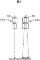
図3に示すように、振動の有無を確認するためには加速度センサASなどを第三カメラCA3に取り付ける方法があるが、この方法だと第三カメラCA3本体に発生する振動の振幅や周波数は把握できても、視野内の画像に発生するぶれの画像上の振幅を把握することは難しく、実際に位置決めアライメントに影響を受けているのかを確認することは難しい。 As shown in FIG. 3, there is a method of attaching an acceleration sensor AS or the like to the third camera CA3 in order to confirm the presence or absence of vibration, but with this method, the amplitude and frequency of the vibration generated in the third camera CA3 main body can be determined. Even if it can be grasped, it is difficult to grasp the amplitude on the image of the blur generated in the image in the visual field, and it is difficult to confirm whether it is actually affected by the positioning alignment.
よって、カメラ内の画像で振動の有無を確認できればよい。画像として振動によってぶれた画像になっていれば、その検出も可能である。しかし、図4(A)に示すように、露光時間に対し振動周期が比較的速ければ画像IMAが滲んで振動していることが分かるが、図4(B)に示すように、露光時間に対し振動周期が比較的遅いと画像IMBは滲まないので分からない。よって、露光時間と振動周波数の関係によっては一括タイミングでシャッタ制御を行うカメラ、例えばCCD撮像素子を用いたカメラ(以下、CCDカメラという。)またはグローバルシャッタ(同時露光一括読出し)のCMOS撮像素子を用いたカメラ(以下、CMOSカメラという。)では確実に検出できるわけではない。 Therefore, it suffices if the presence or absence of vibration can be confirmed from the image in the camera. If the image is blurred due to vibration, it can be detected. However, as shown in FIG. 4 (A), if the vibration cycle is relatively fast with respect to the exposure time, it can be seen that the image IMA is blurred and vibrates, but as shown in FIG. 4 (B), the exposure time On the other hand, if the vibration cycle is relatively slow, the image IMB does not blur, so it is unknown. Therefore, depending on the relationship between the exposure time and the vibration frequency, a camera that controls the shutter at a batch timing, for example, a camera using a CCD image sensor (hereinafter referred to as a CCD camera) or a CMOS image sensor with a global shutter (simultaneous exposure batch read). It cannot be reliably detected by the camera used (hereinafter referred to as a CMOS camera).
熱の影響について以下説明する。
ボンディング工程では、ダイアタッチフィルムを硬化させるために、約80〜160[℃]程度に基板を加熱している。したがって、ダイボンダ内には、加熱等による空気の乱れがある。さらに、搬送動作やピックアップの動作などによって、ダイボンダ内には、気流が発生する。
The effect of heat will be described below.
In the bonding step, the substrate is heated to about 80 to 160 [° C.] in order to cure the die attach film. Therefore, there is air turbulence in the die bonder due to heating or the like. Further, an air flow is generated in the die bonder due to a transfer operation or a pickup operation.
特に、位置決めをするときには、ダイボンディング装置では、撮像装置であるカメラが位置決めしたいターゲット(基板やダイ)を撮像し、画像処理装置が撮像した画像を画像処理してターゲットの基準位置(アライメントマーク)を抽出している。しかし、カメラが撮像する箇所は、熱発生源に近く、気流の動きが激しい。このため、カメラは、気流の動きによる光学的な揺らぎの影響を受ける。また、明るい画像を取得するために、照明の輝度を上げて撮像することが多いが、照明光が照射されることにより発生する熱も無視できない。 In particular, when positioning, in the die bonding device, the camera, which is an imaging device, images the target (board or die) to be positioned, and the image captured by the image processing device is image-processed to perform image processing on the target reference position (alignment mark). Is being extracted. However, the part imaged by the camera is close to the heat source, and the airflow moves violently. Therefore, the camera is affected by optical fluctuations due to the movement of the air flow. Further, in order to acquire a bright image, the brightness of the illumination is often increased to take an image, but the heat generated by the irradiation of the illumination light cannot be ignored.
<第一実施形態>
次に、上述した課題を解決する一例である第一実施形態について図5〜7を用いて説明する。第一実施形態では振動の有無を撮像画像から検出し、振動がある場合は再度撮像を行う。図5は第一実施形態の振動を検出する方法を説明する図であり、図5(A)は振動を検出する構成を示す斜視図であり、図5(B)は振動がある場合の撮像画像である。図6は振動の有無を判断するフローチャートである。図7は振動がある場合の輝線の画像を示す図である。
<First Embodiment>
Next, the first embodiment, which is an example of solving the above-mentioned problems, will be described with reference to FIGS. 5 to 7. In the first embodiment, the presence or absence of vibration is detected from the captured image, and if there is vibration, imaging is performed again. 5A and 5B are views for explaining a method of detecting vibration of the first embodiment, FIG. 5A is a perspective view showing a configuration for detecting vibration, and FIG. 5B is an image taken when there is vibration. It is an image. FIG. 6 is a flowchart for determining the presence or absence of vibration. FIG. 7 is a diagram showing an image of a bright line when there is vibration.
第一実施形態では、撮像毎に画像が振動しているかを検出する。カメラCAにローリングシャッタのCMOSカメラ(ライン露光順次読出し撮像装置)を用いる。図5(A)に示すように、カメラCAの撮像エリアIA内にカメラCAを構成するCMOS撮像素子の水平画素ラインと直交する基準線BLを設ける。 In the first embodiment, it is detected whether the image is vibrating at each imaging. A rolling shutter CMOS camera (line exposure sequential readout imaging device) is used as the camera CA. As shown in FIG. 5A, a reference line BL orthogonal to the horizontal pixel line of the CMOS image sensor constituting the camera CA is provided in the image pickup area IA of the camera CA.
ローリングシャッタは画像上の水平ライン毎に垂直方向に順次シャッタとなるので、図5(B)に示すように、撮像した基準線BLの画像IBLが直線性を失っている場合は、カメラCAが振動していると判断することができる。また、撮像した基準線BLの画像IBLの描く波模様がそのまま振動波形になるため、振幅や周波数が判断でき、その結果から、撮像した画像が振動の影響を受けていても、それがアライメント精度に影響しうるものかを判断することができる。この方法は振動波形の測定方向に指向性があるため、振動方向が明瞭化している場合に用いるとよい。本実施形態は振動の他に陽炎による揺らぎの影響も確認することができる。 Since the rolling shutter becomes a shutter sequentially in the vertical direction for each horizontal line on the image, as shown in FIG. 5B, if the image IBL of the captured reference line BL loses its linearity, the camera CA It can be determined that it is vibrating. In addition, since the wave pattern drawn by the image IBL of the captured reference line BL becomes a vibration waveform as it is, the amplitude and frequency can be determined, and from the result, even if the captured image is affected by the vibration, the alignment accuracy is correct. It is possible to judge whether it can affect the frequency. Since this method has directivity in the measurement direction of the vibration waveform, it is preferable to use this method when the vibration direction is clarified. In this embodiment, in addition to vibration, the influence of fluctuation due to heat haze can also be confirmed.
振動または揺らぎの有無の判断について図6を用いて説明する。
まず、カメラCAによって基準線BLを含む対象物が撮像され、その画像が取得される(ステップS1)。次に、取得した画像から1ライン目の最も明るい画素のx座標を求め、それをLx(1)とする(ステップS2)。次に、取得した画像から2ライン目の最も明るい画素のx座標を求め、それをLx(2)とする(ステップS3)。同様に、取得した画像からNライン(最終ライン)目の最も明るい画素のx座標を求め、それをLx(N)とする(ステップS4)。
The determination of the presence or absence of vibration or fluctuation will be described with reference to FIG.
First, the camera CA captures an object including the reference line BL, and the image is acquired (step S1). Next, the x-coordinate of the brightest pixel of the first line is obtained from the acquired image, and this is designated as Lx (1) (step S2). Next, the x-coordinate of the brightest pixel on the second line is obtained from the acquired image, and this is designated as Lx (2) (step S3). Similarly, the x-coordinate of the brightest pixel of the N-line (final line) eye is obtained from the acquired image, and it is defined as Lx (N) (step S4).
図7に示すように、例えば、iライン目の最も明るい画素のx座標はLx(i)=6、i+8ライン目の最も明るい画素のx座標はLx(i+8)=7、i+15ライン目の最も明るい画素のx座標はLx(i+15)=4である。 As shown in FIG. 7, for example, the x-coordinate of the brightest pixel on the i-line is Lx (i) = 6, the x-coordinate of the brightest pixel on the i + 8th line is Lx (i + 8) = 7, and the x-coordinate of the brightest pixel on the i + 15th line is the most. The x-coordinate of the bright pixel is Lx (i + 15) = 4.
次に、各ラインの最も明るい画素のx座標(Lx(1)〜Lx(N))から最大値(MAX(Lx(1)〜Lx(N)))を求め、また、各ラインの最も明るい画素のx座標(Lx(1)〜Lx(N))から最小値(MIN(Lx(1)〜Lx(N)))を求め、最大値と最小値との差(DEV)を求める(ステップS5)。差(DEV)が所定の閾値(TH)以上かどうかを判断する(ステップS6)。YESの場合、振動または揺らぎがあると判断し、ステップS1に戻る。NOの場合、振動または揺らぎがないと判断し、撮像画像を用いてターゲット認識などによるアライメント処理を行う(ステップS7)。 Next, the maximum value (MAX (Lx (1) to Lx (N))) is obtained from the x-coordinates (Lx (1) to Lx (N)) of the brightest pixel of each line, and the brightest of each line is obtained. The minimum value (MIN (Lx (1) to Lx (N))) is obtained from the x-coordinates (Lx (1) to Lx (N)) of the pixel, and the difference (DEV) between the maximum value and the minimum value is obtained (step). S5). It is determined whether the difference (DEV) is equal to or greater than a predetermined threshold value (TH) (step S6). If YES, it is determined that there is vibration or fluctuation, and the process returns to step S1. If NO, it is determined that there is no vibration or fluctuation, and an alignment process such as target recognition is performed using the captured image (step S7).
第一実施形態では、一括露光方式のカメラ(CCDカメラやグローバルシャッタのCMOSカメラ)ではできない微細時間での時間差処理をもつ露光が可能になるローリングシャッタのCMOSカメラを用いて撮像画像内に微細な時間差処理を与え、本来直線で写るはずの基準線を設け、それが直線であるかを確認することで振動の有無を確認する。ここで、振動を除く撮像タイミングは制御としては、被写体およびカメラは静止している前提である。この方法において、照明システムは常時点灯やストロボ点灯に限るものではない。 In the first embodiment, a rolling shutter CMOS camera is used to enable exposure with a time difference processing in a minute time, which is not possible with a batch exposure type camera (CCD camera or a CMOS camera with a global shutter). The presence or absence of vibration is confirmed by giving a time difference process, providing a reference line that should be captured in a straight line, and checking whether the line is a straight line. Here, the imaging timing excluding vibration is controlled on the premise that the subject and the camera are stationary. In this method, the lighting system is not limited to constant lighting and strobe lighting.
これにより、画像撮像中に、画像に影響を与えうる振動または揺らぎが発生しているかを確認することができる。発生した振動または揺らぎが画像内の座標系において画像ブレとしてどの程度の振幅、周波数、静定時間であるかを測定することができる。撮像した画像が振動または揺らぎの影響を受けていないことを確認することで、画像処理で行う位置決めアライメント精度を対振動または揺らぎ対応として保証できる。振動または揺らぎの影響を受けていることが検出できれば、再認識などのリトライ処理を組み込むことができ、画像処理で行う位置決めアライメント精度を安定させることができる。 This makes it possible to confirm whether vibration or fluctuation that may affect the image is generated during image imaging. It is possible to measure the amplitude, frequency, and static time of the generated vibration or fluctuation as an image blur in the coordinate system in the image. By confirming that the captured image is not affected by vibration or fluctuation, the positioning alignment accuracy performed in the image processing can be guaranteed as a response to vibration or fluctuation. If it can be detected that it is affected by vibration or fluctuation, retry processing such as re-recognition can be incorporated, and the positioning alignment accuracy performed in image processing can be stabilized.
また、振動によるズレが1画素に及ばない場合もしくは画素境界になる場合は、濃淡値の分散からラインの中央を近似計算によって求めてもよい。 Further, when the deviation due to vibration does not reach one pixel or becomes a pixel boundary, the center of the line may be obtained by approximate calculation from the variance of the shading value.
<第二実施形態>
次に、上述した課題を解決する一例である第二実施形態について図8〜10を用いて説明する。第二実施形態では、第一実施形態と同様に、振動の有無を撮像画像から検出し、振動がある場合は再度撮像を行う。図8は第二実施形態の振動を検出する方法を説明する図であり、図8(A)は振動を検出する構成を示す斜視図であり、図8(B)は図8(A)のカメラの構成を示す図である。図9は振動がある場合の撮像画像であり、図9(A)は第一CMOS撮像素子による第一基準線の画像を示す図であり、図9(B)は第二CMOS撮像素子による第二基準線の画像を示す図であり、図9(C)は図9(A)の画像と図9(B)の画像を重ねた図である。図10は振動の有無を判断するフローチャートである。
<Second embodiment>
Next, a second embodiment, which is an example of solving the above-mentioned problems, will be described with reference to FIGS. 8 to 10. In the second embodiment, as in the first embodiment, the presence or absence of vibration is detected from the captured image, and if there is vibration, imaging is performed again. FIG. 8 is a diagram illustrating a method of detecting vibration of the second embodiment, FIG. 8 (A) is a perspective view showing a configuration for detecting vibration, and FIG. 8 (B) is a view of FIG. 8 (A). It is a figure which shows the structure of a camera. FIG. 9 is an image captured when there is vibration, FIG. 9 (A) is a diagram showing an image of the first reference line by the first CMOS image sensor, and FIG. 9 (B) is a diagram showing an image of the first reference line by the second CMOS image sensor. It is a figure which shows the image of the two reference lines, and FIG. 9C is the figure which superposed the image of FIG. 9A and the image of FIG. 9B. FIG. 10 is a flowchart for determining the presence or absence of vibration.
図8(A)に示すように、第二実施形態のカメラCAAの撮像エリアIA内に第一基準線BL1と第一基準線BL1が延伸する方向と直交する方向に延伸する第二基準線BL2を設ける。 As shown in FIG. 8A, the first reference line BL1 and the second reference line BL2 extending in the direction orthogonal to the extending direction in the imaging area IA of the camera CAA of the second embodiment. Is provided.
図8(B)に示すように、カメラCAAは第一CMOS撮像素子IPD1と第二CMOS撮像素子IPD2と第一プリズムPR1と第二プリズムPR2とを備える。カメラCAAへの入射光ILは第一プリズムPR1と第二プリズムPR2とにより、第一入射光IL1と第二入射光IL2に分かれ、第一入射光IL1は第一CMOS撮像素子IPD1に入射し、第二入射光IL2は第二CMOS撮像素子IPD2に入射する。第一CMOS撮像素子IPD1の水平画素ラインの方向(矢印H1の方向)と第一基準線BL1が延伸する方向が直交するように、第一CMOS撮像素子IPD1が配置される。また、第二CMOS撮像素子IPD2の水平画素ラインの方向(矢印H2の方向)と第二基準線BL2が延伸する方向が直交するように、第二CMOS撮像素子IPD2とが配置される。 As shown in FIG. 8B, the camera CAA includes a first CMOS image sensor IPD1, a second CMOS image sensor IPD2, a first prism PR1, and a second prism PR2. The incident light IL to the camera CAA is divided into a first incident light IL1 and a second incident light IL2 by the first prism PR1 and the second prism PR2, and the first incident light IL1 is incident on the first CMOS image sensor IPD1. The second incident light IL2 is incident on the second CMOS image sensor IPD2. The first CMOS image sensor IPD1 is arranged so that the direction of the horizontal pixel line of the first CMOS image sensor IPD1 (the direction of the arrow H1) and the direction in which the first reference line BL1 extends are orthogonal to each other. Further, the second CMOS image sensor IPD2 is arranged so that the direction of the horizontal pixel line of the second CMOS image sensor IPD2 (the direction of the arrow H2) and the direction in which the second reference line BL2 extends are orthogonal to each other.
図9(A)に示すように、第一撮像素子IPD1で撮像された第一基準線BL1の画像IBL1に歪みがある場合、第一撮像素子IPD1で撮像された第一画像IM1の領域WA1は振動で画像が歪んだ領域となる。図9(B)に示すように、第二撮像素子IPD2で撮像された第二基準線BL2の画像IBL2に歪みがある場合、第二撮像素子IPD2で撮像された第二画像IM2の領域WA2は振動で画像が歪んだ領域となる。よって、図9(C)の破線で示した第一領域DA1と第二領域DA2に、第一画像IM1と第二画像IM2との差異が現れる。 As shown in FIG. 9A, when the image IBL1 of the first reference line BL1 imaged by the first image sensor IPD1 is distorted, the region WA1 of the first image IM1 imaged by the first image sensor IPD1 is The image becomes a distorted area due to vibration. As shown in FIG. 9B, when the image IBL2 of the second reference line BL2 imaged by the second image sensor IPD2 is distorted, the region WA2 of the second image IM2 imaged by the second image sensor IPD2 is The image becomes a distorted area due to vibration. Therefore, the difference between the first image IM1 and the second image IM2 appears in the first region DA1 and the second region DA2 shown by the broken line in FIG. 9C.
振動または揺らぎの有無の判断について図10を用いて説明する。
まず、カメラCAAによって第一基準線BL1および第二基準線BL2を含む対象物(例えば、基板やダイ)が撮像され、第一CMOS撮像素子IPD1および第二CMOS撮像素子IPD2が同時にその第一画像IM1および第二画像IM2を取得する(ステップS11)。次に、カメラCAAは第一画像IM1および第二画像IM2を制御装置に転送する(ステップS12)。制御装置は、第一CMOS撮像素子IPD1が撮像した第一画像IM1と第二CMOS撮像素子IPD2が撮像した第二画像IM2を差分し、絶対値変換する(ステップS13)。制御装置は、画像内に所定の閾値以上の明度を有する領域(例えば、第一領域DA1、第二領域DA2)があるかどうか判断する(ステップS14)。YESの場合、振動または揺らぎがあると判断し、ステップS11に戻る。NOの場合、振動または揺らぎがないと判断し、第一画像IM1または第二画像IM2のいずれかの画像を用いてターゲット認識などによるアライメント処理を行う(ステップS15)。
The determination of the presence or absence of vibration or fluctuation will be described with reference to FIG.
First, an object (for example, a substrate or a die) including the first reference line BL1 and the second reference line BL2 is imaged by the camera CAA, and the first CMOS image sensor IPD1 and the second CMOS image sensor IPD2 simultaneously perform the first image. The IM1 and the second image IM2 are acquired (step S11). Next, the camera CAA transfers the first image IM1 and the second image IM2 to the control device (step S12). The control device makes a difference between the first image IM1 imaged by the first CMOS image sensor IPD1 and the second image IM2 imaged by the second CMOS image sensor IPD2, and converts them into absolute values (step S13). The control device determines whether or not there is a region (for example, first region DA1 and second region DA2) having a brightness equal to or higher than a predetermined threshold value in the image (step S14). If YES, it is determined that there is vibration or fluctuation, and the process returns to step S11. If NO, it is determined that there is no vibration or fluctuation, and an alignment process such as target recognition is performed using either the first image IM1 or the second image IM2 (step S15).
第二実施形態によれば、1方向の振動しか測定できなかった第一実施形態に比べ、XY方向での測定ができるようになる。この方法を用いれば、振動のベクトル方向も検出することができるようになる。 According to the second embodiment, the measurement in the XY direction can be performed as compared with the first embodiment in which the vibration in only one direction can be measured. By using this method, the vector direction of vibration can also be detected.
<第三実施形態>
上述した課題の解決手段の一例である第三実施形態について図11〜14を用いて説明する。第三実施形態では、陽炎による揺らぎを検出した場合、第一実施形態や第二実施形態のように再度撮像するのではなく、撮像画像を補正する。
<Third Embodiment>
The third embodiment, which is an example of the means for solving the above-mentioned problems, will be described with reference to FIGS. 11 to 14. In the third embodiment, when the fluctuation due to the heat haze is detected, the captured image is corrected instead of re-imaging as in the first embodiment and the second embodiment.
図11は第三実施形態の陽炎による揺らぎを検出する方法を説明する図であり、基板のダイ搭載領域およびその周辺の画像であり、揺らぎにより歪みがある画像を示す図である。図12は第三実施形態の陽炎による揺らぎを検出する方法を説明する図であり、アライメントパターンと基準線との関係を示す画像である。図13は倣い動作のフローチャートである。図14は連続着工動作のフローチャートである。 FIG. 11 is a diagram illustrating a method of detecting fluctuations due to the heat haze of the third embodiment, is an image of a die mounting area of a substrate and its surroundings, and is a diagram showing an image distorted due to fluctuations. FIG. 12 is a diagram illustrating a method of detecting fluctuations due to the heat haze of the third embodiment, and is an image showing the relationship between the alignment pattern and the reference line. FIG. 13 is a flowchart of the copying operation. FIG. 14 is a flowchart of the continuous construction start operation.
図11に示すように、アライメントパターンの画像IAMに揺らぎによる歪みが発生すると、画像IAM近傍のダイ搭載領域の境界線等本来真っ直ぐ写るべき所SPも揺らぎで歪む。したがって、カメラで撮像しているときに、陽炎による揺らぎがあった場合、その揺らぎによってアライメントパターンが動いてしまう。上述したように、グローバルシャッタのカメラでは動いてしまっていること自体がわからないが、ローリングシャッタのカメラでは既知の直線部分が歪んでいるかどうかで、影響を受けているかどうかの判断がつく。ここで、アライメントパターンと基準線の陽炎の揺らぎが同一波形になるよう、基準線としてアライメントパターンにできるだけ近い直線を使用する。 As shown in FIG. 11, when the image IAM of the alignment pattern is distorted due to fluctuations, the SP where the image IAM should be captured straight, such as the boundary line of the die mounting area near the image IAM, is also distorted due to the fluctuations. Therefore, if there is a fluctuation due to the heat haze when the image is taken by the camera, the alignment pattern moves due to the fluctuation. As mentioned above, it is not known that the camera with the global shutter has moved, but with the camera with the rolling shutter, it can be judged whether or not it is affected by whether or not the known straight line part is distorted. Here, a straight line as close as possible to the alignment pattern is used as the reference line so that the alignment pattern and the fluctuation of the heat haze of the reference line have the same waveform.
図12に示すように、既知の直線部分の境界検出を多点で行い、ハフ(Hough)変換や最小二乗法による近似処理で、その直線の真値を検出する(近似直線ASLを導く)。近似直線ASLがアライメントパターンと同一水平ライン上が歪んでいることが検出されれば、アレイメントマークと同一水平ライン上(同位相)にある境界位置から歪みオフセットを測定し、アライメントパターンの位置決め結果をその歪みオフセット分だけ補正することで、陽炎による揺らぎの影響を除去することができる。以下、詳細について図13、14を用いて説明する。 As shown in FIG. 12, the boundary of a known straight line portion is detected at multiple points, and the true value of the straight line is detected by the Hough transform or the approximation process by the least squares method (the approximate straight line ASL is derived). If it is detected that the approximate straight line ASL is distorted on the same horizontal line as the alignment pattern, the distortion offset is measured from the boundary position on the same horizontal line (in phase) as the arrayment mark, and the alignment result is positioned. Is corrected by the amount of the distortion offset, so that the influence of the fluctuation due to the heat haze can be eliminated. Hereinafter, details will be described with reference to FIGS. 13 and 14.
まず、倣い動作として、図13に示すように、位置決めに用いるアライメントパターンAPと基準線SLPを撮像し画像を取り込む(ステップS21)。アライメントパターンAPの位置を登録する(ステップS22)。このとき、位置決めアルゴリズムにパターンマッチングを用いるのであれば、モデル画像の登録も行う。アライメントパターンAPと同じ水平ライン上を直交する基準線SLPの位置を登録する(ステップS23)。 First, as a copying operation, as shown in FIG. 13, the alignment pattern AP and the reference line SLP used for positioning are imaged and an image is captured (step S21). The position of the alignment pattern AP is registered (step S22). At this time, if pattern matching is used for the positioning algorithm, the model image is also registered. The position of the reference line SLP orthogonal to the alignment pattern AP on the same horizontal line is registered (step S23).
次に、連続着工動作として、図14に示すように、位置決めに用いるアライメントパターンAPと基準線SLPを撮像し画像を取り込む(ステップS31)。撮像したアレイメントパターンの画像IMAからアライメントパターンAPの位置を測定する(ステップS32)。測定したアライメントパターンから登録した基準線の位置のあるべき場所を算出し、その付近での直線検出を行い、近似直線ASLを求める(ステップS33)。直線の前後部分(図面上、アライメントパターンよりも上または下に対応する部分)に比べ、アライメントパターン付近の位置にずれがある場合(陽炎による揺らぎによって直線の変形を検出した場合)、そのずれを測定する(ステップS34)。測定結果をアライメントパターンの位置決め結果にフィードバックし、ダイの位置ずれを補正する(ステップS35)。 Next, as a continuous construction start operation, as shown in FIG. 14, the alignment pattern AP and the reference line SLP used for positioning are imaged and the images are captured (step S31). The position of the alignment pattern AP is measured from the image IMA of the captured arrayment pattern (step S32). From the measured alignment pattern, the position where the registered reference line should be located is calculated, a straight line is detected in the vicinity thereof, and an approximate straight line ASL is obtained (step S33). If there is a deviation in the position near the alignment pattern (when deformation of the straight line is detected due to fluctuations due to heat haze) compared to the front and back parts of the straight line (the part corresponding to above or below the alignment pattern in the drawing), the deviation is Measure (step S34). The measurement result is fed back to the positioning result of the alignment pattern, and the misalignment of the die is corrected (step S35).
上述した実施形態をダイボンダに適用した例について以下説明する。 An example in which the above-described embodiment is applied to a die bonder will be described below.
図15は実施例に係るダイボンダの概略を示す上面図である。図16は図15において矢印A方向から見たときに、ピックアップヘッド及びボンディングヘッドの動作を説明する図である。 FIG. 15 is a top view showing an outline of the die bonder according to the embodiment. FIG. 16 is a diagram illustrating the operation of the pickup head and the bonding head when viewed from the direction of arrow A in FIG.
ダイボンダ10は、大別して、一つ又は複数の最終1パッケージとなる製品エリア(以下、パッケージエリアPという。)をプリントした基板Sに実装するダイDを供給する供給部1と、ピックアップ部2、中間ステージ部3と、ボンディング部4と、搬送部5、基板供給部6と、基板搬出部7と、各部の動作を監視し制御する制御部8と、を有する。Y軸方向がダイボンダ10の前後方向であり、X軸方向が左右方向である。ダイ供給部1がダイボンダ10の手前側に配置され、ボンディング部4が奥側に配置される。
The
まず、ダイ供給部1は基板SのパッケージエリアPに実装するダイDを供給する。ダイ供給部1は、ウェハ11を保持するウェハ保持台12と、ウェハ11からダイDを突き上げる点線で示す突上げユニット13と、を有する。ダイ供給部1は図示しない駆動手段によってXY方向に移動し、ピックアップするダイDを突上げユニット13の位置に移動させる。
First, the
ピックアップ部2は、ダイDをピックアップするピックアップヘッド21と、ピックアップヘッド21をY方向に移動させるピックアップヘッドのY駆動部23と、コレット22を昇降、回転及びX方向移動させる図示しない各駆動部と、を有する。ピックアップヘッド21は、突き上げられたダイDを先端に吸着保持するコレット22(図2も参照)を有し、ダイ供給部1からダイDをピックアップし、中間ステージ31に載置する。ピックアップヘッド21は、コレット22を昇降、回転及びX方向移動させる図示しない各駆動部を有する。
The
中間ステージ部3は、ダイDを一時的に載置する中間ステージ31と、中間ステージ31上のダイDを認識する為のステージ認識カメラ32を有する。
The
ボンディング部4は、中間ステージ31からダイDをピックアップし、搬送されてくる基板SのパッケージエリアP上にボンディングし、又は既に基板SのパッケージエリアPの上にボンディングされたダイの上に積層する形でボンディングする。ボンディング部4は、ピックアップヘッド21と同様にダイDを先端に吸着保持するコレット42(図2も参照)を備えるボンディングヘッド41と、ボンディングヘッド41をY方向に移動させるY駆動部43と、基板SのパッケージエリアPの位置認識マーク(図示せず)を撮像し、ボンディング位置を認識する基板認識カメラ44とを有する。
このような構成によって、ボンディングヘッド41は、ステージ認識カメラ32の撮像データに基づいてピックアップ位置・姿勢を補正し、中間ステージ31からダイDをピックアップし、基板認識カメラ44の撮像データに基づいて基板にダイDをボンディングする。
The
With such a configuration, the
搬送部5は、基板Sを掴み搬送する基板搬送爪51と、基板Sが移動する搬送レーン52と、を有する。基板Sは、搬送レーン52に設けられた基板搬送爪51の図示しないナットを搬送レーン52に沿って設けられた図示しないボールネジで駆動することによって移動する。
このような構成によって、基板Sは、基板供給部6から搬送レーン52に沿ってボンディング位置まで移動し、ボンディング後、基板搬出部7まで移動して、基板搬出部7に基板Sを渡す。
The
With such a configuration, the substrate S moves from the
制御部8は、ダイボンダ10の各部の動作を監視し制御するプログラム(ソフトウェア)を格納するメモリと、メモリに格納されたプログラムを実行する中央処理装置(CPU)と、を備える。
The
次に、ダイ供給部1の構成について図17および図18を用いて説明する。図17はダイ供給部の外観斜視図を示す図である。図18はダイ供給部の主要部を示す概略断面図である。
Next, the configuration of the
ダイ供給部1は、水平方向(XY方向)に移動するウェハ保持台12と、上下方向に移動する突上げユニット13と、を備える。ウェハ保持台12は、ウェハリング14を保持するエキスパンドリング15と、ウェハリング14に保持され複数のダイDが接着されたダイシングテープ16を水平に位置決めする支持リング17と、を有する。突上げユニット13は支持リング17の内側に配置される。
The
ダイ供給部1は、ダイDの突き上げ時に、ウェハリング14を保持しているエキスパンドリング15を下降させる。その結果、ウェハリング14に保持されているダイシングテープ16が引き伸ばされダイDの間隔が広がり、突上げユニット13によりダイD下方よりダイDを突き上げ、ダイDのピックアップ性を向上させている。なお、薄型化に伴いダイを基板に接着する接着剤は、液状からフィルム状となり、ウェハ11とダイシングテープ16との間にダイアタッチフィルム(DAF)18と呼ばれるフィルム状の接着材料を貼り付けている。ダイアタッチフィルム18を有するウェハ11では、ダイシングは、ウェハ11とダイアタッチフィルム18に対して行なわれる。従って、剥離工程では、ウェハ11とダイアタッチフィルム18をダイシングテープ16から剥離する。
The
ダイボンダ10は、ウェハ11上のダイDの姿勢を認識するウェハ認識カメラ24と、中間ステージ31に載置されたダイDの姿勢を認識するステージ認識カメラ32と、ボンディングステージBS上の実装位置を認識する基板認識カメラ44とを有する。認識カメラ間の姿勢ずれ補正しなければならないのは、ボンディングヘッド41によるピックアップに関与するステージ認識カメラ32と、ボンディングヘッド41による実装位置へのボンディングに関与する基板認識カメラ44である。本実施例ではステージ認識カメラ32はローリングシャッタのCMOSカメラを用い、ステージ認識カメラ32の撮像エリア内の中間ステージ31のダイプレース位置近傍にステージ認識カメラ32を構成するCMOS撮像素子の水平画素ラインと直交する輝線(第一実施形態または第二実施形態の基準線の一例)を設ける。また、基板認識カメラ44はローリングシャッタのCMOSカメラを用い、基板認識カメラ44の撮像エリア内のボンディングエリアのクランパ部に基板認識カメラ44を構成するCMOS撮像素子の水平画素ラインと直交する輝線(第一実施形態または第二実施形態の基準線の一例)を設ける。
The
制御部8について図19を用いて説明する。図19は制御系の概略構成を示すブロック図である。制御系80は制御部8と駆動部86と信号部87と光学系88とを備える。制御部8は、大別して、主としてCPU(Central Processor Unit)で構成される制御・演算装置81と、記憶装置82と、入出力装置83と、バスライン84と、電源部85とを有する。記憶装置82は、処理プログラムなどを記憶しているRAMで構成されている主記憶装置82aと、制御に必要な制御データや画像データ等を記憶しているHDDやSSD等で構成されている補助記憶装置82bとを有する。入出力装置83は、装置状態や情報等を表示するモニタ83aと、オペレータの指示を入力するタッチパネル83bと、モニタを操作するマウス83cと、光学系88からの画像データを取り込む画像取込装置83dと、を有する。また、入出力装置83は、ダイ供給部1のXYテーブル(図示せず)やボンディングヘッドテーブルのZY駆動軸等の駆動部86を制御するモータ制御装置83eと、種々のセンサ信号や照明装置などのスイッチ等の信号部87から信号を取り込み又は制御するI/O信号制御装置83fとを有する。光学系88には、ウェハ認識カメラ24、ステージ認識カメラ32、基板認識カメラ44が含まれる。制御・演算装置81はバスライン84を介して必要なデータを取込み、演算し、ピックアップヘッド21等の制御や、モニタ83a等に情報を送る。
The
制御部8は画像取込装置83dを介してウェハ認識カメラ24、ステージ認識カメラ32および基板認識カメラ44で撮像した画像データを記憶装置82に保存する。保存した画像データに基づいてプログラムしたソフトウェアにより、制御・演算装置81を用いてダイDおよび基板SのパッケージエリアPの位置決め、並びにダイDおよび基板Sの表面検査を行う。制御・演算装置81が算出したダイDおよび基板SのパッケージエリアPの位置に基づいてソフトウェアによりモータ制御装置83eを介して駆動部86を動かす。このプロセスによりウェハ上のダイの位置決めを行い、ピックアップ部2およびボンディング部4の駆動部で動作させダイDを基板SのパッケージエリアP上にボンディングする。使用するウェハ認識カメラ24、ステージ認識カメラ32および基板認識カメラ44はグレースケール、カラー等であり、光強度を数値化する。
The
図20は図15のダイボンダにおけるダイボンディング工程を説明するフローチャートである。
実施例のダイボンディング工程では、まず、制御部8は、ウェハ11を保持しているウェハリング14をウェハカセットから取り出してウェハ保持台12に載置し、ウェハ保持台12をダイDのピックアップが行われる基準位置まで搬送する(ウェハローディング(工程P1))。次いで、制御部8は、ウェハ認識カメラ24によって取得した画像から、ウェハ11の配置位置がその基準位置と正確に一致するように微調整を行う。
FIG. 20 is a flowchart illustrating a die bonding process in the die bonder of FIG.
In the die bonding step of the embodiment, first, the
次に、制御部8は、ウェハ11が載置されたウェハ保持台12を所定ピッチでピッチ移動させ、水平に保持することによって、最初にピックアップされるダイDをピックアップ位置に配置する(ダイ搬送(工程P2))。ウェハ11は、予めプローバ等の検査装置により、ダイ毎に検査され、ダイ毎に良、不良を示すマップデータが生成され、制御部8の記憶装置82に記憶される。ピックアップ対象となるダイDが良品であるか、不良品であるかの判定はマップデータにより行われる。制御部8は、ダイDが不良品である場合は、ウェハ11が載置されたウェハ保持台12を所定ピッチでピッチ移動させ、次にピックアップされるダイDをピックアップ位置に配置し、不良品のダイDをスキップする。
Next, the
制御部8は、ウェハ認識カメラ24によってピックアップ対象のダイDの主面(上面)を撮像し、取得した画像からピックアップ対象のダイDの上記ピックアップ位置からの位置ずれ量を算出する。制御部8は、この位置ずれ量を基にウェハ11が載置されたウェハ保持台12を移動させ、ピックアップ対象のダイDをピックアップ位置に正確に配置する(ダイ位置決め(工程P3))。
The
次いで、制御部8は、ウェハ認識カメラ24によって取得した画像から、ダイDの表面検査を行う(工程P4)。ここで、制御部8は、表面検査で問題があるかどうかを判定し、ダイDの表面に問題なしと判定した場合には次工程(後述する工程P9)へ進むが、問題ありと判定した場合には、表面画像を目視で確認するか、さらに高感度の検査や照明条件などを変えた検査を行い、問題がある場合はスキップ処理し、問題がない場合は次工程の処理を行う。スキップ処理は、ダイDの工程P9以降をスキップし、ウェハ11が載置されたウェハ保持台12を所定ピッチでピッチ移動させ、次にピックアップされるダイDをピックアップ位置に配置する。
Next, the
制御部8は、基板供給部6で基板S搬送レーン52に載置する(基板ローディング(工程P5))。制御部8は、基板Sを掴み搬送する基板搬送爪51をボンディング位置まで移動させる(基板搬送(工程P6))。
The
基板認識カメラ44にて基板Sおよび輝線を撮像し、位置決めを行う(基板位置決め(工程P7))。第一実施形態または第二実施形態の判断方法により、撮像した輝線の画像から振動しているかどうかを判断し、振動していないと判断する場合は位置決めを行う。振動していると判断する場合は、基板認識カメラ44は再度画像を取得する。
The
次いで、制御部8は、基板認識カメラ44によって取得した画像から、基板SのパッケージエリアPの表面検査を行う(工程P8)。ここで、制御部8は、表面検査で問題があるかどうかを判定し、基板SのパッケージエリアPの表面に問題なしと判定した場合には次工程(後述する工程P9)へ進むが、問題ありと判定した場合には、表面画像を目視で確認するか、さらに高感度の検査や照明条件などを変えた検査を行い、問題がある場合はスキップ処理し、問題がない場合は次工程の処理を行う。スキップ処理は、基板SのパッケージエリアPの該当タブへの工程P10以降をスキップし、基板着工情報に不良登録を行う。
Next, the
制御部8は、ダイ供給部1によってピックアップ対象のダイDを正確にピックアップ位置に配置した後、コレット22を含むピックアップヘッド21によってダイDをダイシングテープ16からピックアップし(ダイハンドリング(工程P9))、中間ステージ31に載置する((工程P10)。制御部8は、中間ステージ31に載置したダイの姿勢ずれ(回転ずれ)の検出をステージ認識カメラ32にてダイDおよび輝線を撮像して行う(工程P11)。第一実施形態または第二実施形態の判断方法により、撮像した輝線の画像から振動しているかどうかを判断し、振動していないと判断する場合、ダイの姿勢ずれ(回転ずれ)の検出を行う。振動していると判断する場合は、ステージ認識カメラ32は再度画像を取得する。制御部8は、姿勢ずれがある場合は中間ステージ31に設けられた旋回駆動装置(不図示)によって実装位置を有する実装面に平行な面で中間ステージ31を旋回させて姿勢ずれを補正する。
The
制御部8は、ステージ認識カメラ32によって取得した画像から、ダイDの表面検査を行う(工程P12)。ここで、制御部8は、表面検査で問題があるかどうかを判定し、ダイDの表面に問題なしと判定した場合には次工程(後述する工程P13)へ進むが、問題ありと判定した場合には、表面画像を目視で確認するか、さらに高感度の検査や照明条件などを変えた検査を行い、問題がある場合は、そのダイを図示しない不良品トレーなどに載置してスキップ処理し、問題がない場合は次工程の処理を行う。スキップ処理は、ダイDの工程P13以降をスキップし、ウェハ11が載置されたウェハ保持台12を所定ピッチでピッチ移動させ、次にピックアップされるダイDをピックアップ位置に配置する。
The
制御部8は、コレット42を含むボンディングヘッド41によって中間ステージ31からダイDをピックアップし、基板SのパッケージエリアPまたは既に基板SのパッケージエリアPにボンディングされているダイにダイボンディングする(ダイアタッチ((工程P13))。
The
制御部8は、ダイDをボンディングした後、そのボンディング位置が正確になされているかをダイD、基板Sおよび輝線を基板認識カメラ44で撮像して検査する(ダイと基板の相対位置検査(工程P14))。第一実施形態または第二実施形態の判断方法により、撮像した輝線の画像から振動しているかどうかを判断し、振動していないと判断する場合、ボンディング位置が正確になされているかの検査を行う。振動していると判断する場合は、基板認識カメラ44は再度画像を取得する。このとき、ダイの位置合わせと同様にダイの中心と、タブの中心を求め、相対位置が正しいかを検査する。
After bonding the die D, the
次いで、制御部8は、基板認識カメラ44によって取得した画像から、ダイDおよび基板Sの表面検査を行う(工程P15)。ここで、制御部8は、表面検査で問題があるかどうかを判定し、ボンディングされたダイDの表面に問題なしと判定した場合には次工程(後述する工程P9)へ進むが、問題ありと判定した場合には、表面画像を目視で確認するか、さらに高感度の検査や照明条件などを変えた検査を行い、問題がある場合はスキップ処理し、問題がない場合は次工程の処理を行う。スキップ処理では、基板着工情報に不良登録を行う。
Next, the
以後、同様の手順に従ってダイDが1個ずつ基板SのパッケージエリアPにボンディングする。1つの基板のボンディングが完了すると、基板搬送爪51で基板Sを基板搬出部7まで移動して(基板搬送(工程P16))、基板搬出部7に基板Sを渡す(基板アンローディング(工程P17))。
After that, the dies D are bonded to the package area P of the substrate S one by one according to the same procedure. When the bonding of one substrate is completed, the substrate S is moved to the
以後、同様の手順に従ってダイDが1個ずつダイシングテープ16から剥がされる(工程P9)。不良品を除くすべてのダイDのピックアップが完了すると、それらダイDをウェハ11の外形で保持していたダイシングテープ16およびウェハリング14等をウェハカセットへアンローディングする(工程P18)。
After that, the dies D are peeled off from the dicing
以上、本発明者によってなされた発明を実施例および変形例に基づき具体的に説明したが、本発明は、上記実施例および変形例に限定されるものではなく、種々変更可能であることはいうまでもない。 The invention made by the present inventor has been specifically described above based on Examples and Modifications, but the present invention is not limited to the above Examples and Modifications, and can be variously modified. Not to mention.
例えば、第二実施形態では、基準線を設けて振動の有無を判断する例を説明したが、第一CMOS撮像素子IPD1および第二CMOS撮像素子IPD2の両方が正方格子のセルを有するものであれば、両画像を差分比較によって見比べ、不一致領域があれば、基準線を設けなくても振動の有無がわかるようになる。 For example, in the second embodiment, an example in which a reference line is provided to determine the presence or absence of vibration has been described, but both the first CMOS image sensor IPD1 and the second CMOS image sensor IPD2 may have cells in a square lattice. For example, both images are compared by difference comparison, and if there is a mismatched region, the presence or absence of vibration can be known without providing a reference line.
また、実施例では基準線として輝線を例に説明したが、輝線は発光するものに限らず、反射性のものや、単なる模様、レーザによる投影でもよい。 Further, in the embodiment, the emission line has been described as an example as the reference line, but the emission line is not limited to the one that emits light, and may be a reflective one, a simple pattern, or a projection by a laser.
また、実施例では、第一実施形態または第二実施形態による振動を判断する方法を適用する例を説明したが、第三実施形態による揺らぎを判断する方法を適用してもよい。 Further, in the examples, the method of determining the vibration according to the first embodiment or the second embodiment has been described, but the method of determining the fluctuation according to the third embodiment may be applied.
また、実施例では、ステージ認識カメラおよび基板認識カメラによる撮像において第一実施形態または第二実施形態を適用する例について説明したが、ウェハ認識カメラによる撮像において第一実施形態または第二実施形態を適用してもよい。
また、実施例ではダイ位置認識の後にダイ外観検査認識を行っているが、ダイ外観検査認識の後にダイ位置認識を行ってもよい。
また、実施例ではウェハの裏面にDAFが貼付されているが、DAFはなくてもよい。
また、実施例ではピックアップヘッドおよびボンディングヘッドをそれぞれ1つ備えているが、それぞれ2つ以上であってもよい。また、実施例では中間ステージを備えているが、中間ステージがなくてもよい。この場合、ピックアップヘッドとボンディングヘッドは兼用してもよい。
また、実施例ではダイの表面を上にしてボンディングされるが、ダイをピックアップ後ダイの表裏を反転させて、ダイの裏面を上にしてボンディングしてもよい。この場合、中間ステージは設けなくてもよい。この装置はフリップチップボンダという。
Further, in the embodiment, an example in which the first embodiment or the second embodiment is applied in the imaging by the stage recognition camera and the substrate recognition camera has been described, but the first embodiment or the second embodiment is used in the imaging by the wafer recognition camera. May be applied.
Further, in the embodiment, the die appearance inspection recognition is performed after the die position recognition, but the die position recognition may be performed after the die appearance inspection recognition.
Further, in the embodiment, the DAF is attached to the back surface of the wafer, but the DAF may not be present.
Further, in the embodiment, one pickup head and one bonding head are provided, but two or more of each may be provided. Further, although the intermediate stage is provided in the embodiment, the intermediate stage may not be provided. In this case, the pickup head and the bonding head may be used in combination.
Further, in the embodiment, the die is bonded with the front surface facing up, but after picking up the die, the front and back surfaces of the die may be inverted and the die may be bonded with the back surface facing up. In this case, the intermediate stage may not be provided. This device is called a flip chip bonder.
10・・・ダイボンダ
1・・・ダイ供給部
13・・・突上げユニット
2・・・ピックアップ部
24・・・ウェハ認識カメラ
3・・・中間ステージ部
31・・・中間ステージ
32・・・ステージ認識カメラ
4・・・ボンディング部
41・・・ボンディングヘッド
42・・・コレット
44・・・基板認識カメラ
5・・・搬送部
51・・・基板搬送爪
8・・・制御部
S・・・基板
BS・・・ボンディングステージ
D・・・ダイ
P・・・パッケージエリア
CA・・・カメラ
BL・・・基準線
IA・・・撮像エリア
IBL・・・基準線の画像
10 ... Die
Claims (13)
基板またはダイの近傍であって前記撮像装置の撮像領域内に配置され、前記第一CMOS撮像素子の水平画素ラインと直交する方向に延伸する第一基準線と、
前記撮像装置を制御する制御装置と、
を備え、
前記制御装置は、前記撮像装置が前記基板または前記ダイと同一露光で撮像する前記第一基準線の画像に基づいて振動または陽炎による揺らぎを検出するダイボンディング装置。 An image pickup device that has a first CMOS image sensor and sequentially reads out line exposures,
A first reference line that is located near the substrate or die and is located in the image pickup region of the image pickup device and extends in a direction orthogonal to the horizontal pixel line of the first CMOS image pickup device.
A control device that controls the image pickup device and
With
The control device is a die bonding device that detects fluctuations due to vibration or heat haze based on an image of the first reference line imaged by the image pickup device with the same exposure as the substrate or the die.
前記制御装置は、前記第一基準線の画像が所定値以上ずれている場合、前記振動または前記揺らぎがあると判断するダイボンディング装置。 In claim 1,
The control device is a die bonding device that determines that there is the vibration or the fluctuation when the image of the first reference line deviates by a predetermined value or more.
前記制御装置は、前記撮像装置による前記基板または前記ダイの撮像をやり直すダイボンディング装置。 In claim 2,
The control device is a die bonding device that redoes the imaging of the substrate or the die by the imaging device.
さらに、前記基板または前記ダイの近傍であって前記撮像装置の撮像領域内に配置され、前記第一基準線が延伸する方向と直交する方向に延伸する第二基準線を備え、
前記撮像装置は、さらに、前記第二基準線が延伸する方向と直交する方向に水平画素ラインがある第二CMOS撮像素子を備え、
前記制御装置は、前記撮像装置が前記基板または前記ダイと前記第一基準線と前記第二基準線とを同一露光で撮像する前記第一CMOS撮像素子の画像および前記第二CMOS撮像素子の画像に基づいて振動または陽炎による揺らぎを検出するダイボンディング装置。 In claim 1,
Further, it is provided with a second reference line which is arranged in the imaging region of the imaging apparatus in the vicinity of the substrate or the die and extends in a direction orthogonal to the extending direction of the first reference line.
The image pickup device further includes a second CMOS image pickup device having a horizontal pixel line in a direction orthogonal to the direction in which the second reference line extends.
The control device includes an image of the first CMOS image sensor and an image of the second CMOS image sensor on which the image pickup device captures the substrate or the die, the first reference line, and the second reference line with the same exposure. A die bonding device that detects fluctuations due to vibration or heat haze based on.
前記制御装置は、前記第一CMOS撮像素子の画像と前記第二CMOS撮像素子の画像を差分し絶対値変換しその画像に所定値以上の明度を有する場合、前記振動または前記揺らぎがあると判断するダイボンディング装置。 In claim 4,
The control device differentiates the image of the first CMOS image sensor and the image of the second CMOS image sensor, converts them into absolute values, and determines that the image has the vibration or the fluctuation when the image has a brightness equal to or higher than a predetermined value. Die bonding equipment.
前記制御装置は、前記撮像装置による前記基板または前記ダイの撮像をやり直すダイボンディング装置。 In claim 5,
The control device is a die bonding device that redoes the imaging of the substrate or the die by the imaging device.
さらに、前記第一基準線の近傍にアライメントパターンを備え、
前記制御装置は、前記第一基準線の前記アライメントパターンに対向する位置にずれがある場合、そのずれを測定し、その測定結果を前記アライメントパターンの位置決め結果にフィードバックするダイボンディング装置。 In claim 1,
Further, an alignment pattern is provided in the vicinity of the first reference line.
The control device is a die bonding device that measures a deviation in a position of the first reference line facing the alignment pattern and feeds back the measurement result to a positioning result of the alignment pattern.
前記ダイをピックアップするピックアップヘッドを備え、
前記制御装置は前記撮像装置を用いて前記基板および前記基板の近傍に設けられた前記第一基準線を撮像するダイボンディング装置。 In claim 1, further
Equipped with a pickup head to pick up the die
The control device is a die bonding device that uses the image pickup device to image the substrate and the first reference line provided in the vicinity of the substrate.
前記ダイをピックアップするピックアップヘッドと、
ピックアップされた前記ダイが載置される中間ステージと、
を備え、
前記制御装置は前記撮像装置を用いて前記中間ステージの上に載置された前記ダイおよび前記中間ステージに設けられた前記第一基準線を撮像するダイボンディング装置。 In claim 1, the pickup head for further picking up the die and the pickup head
The intermediate stage on which the picked-up die is placed and
With
The control device is a die bonding device that uses the image pickup device to image the die mounted on the intermediate stage and the first reference line provided on the intermediate stage.
(b)ダイが貼付されたダイシングテープを保持するウェハリングホルダを搬入する工程と、
(c)基板を搬入する工程と、
(d)前記ダイをピックアップする工程と、
(e)ピックアップした前記ダイを前記基板または既に前記基板にボンディングされているダイ上にボンディングする工程と、
を備え、
前記(d)工程または前記(e)工程において、前記撮像装置が前記基板または前記ダイと同一露光で撮像する前記第一基準線の画像に基づいて振動または陽炎による揺らぎを検出する半導体装置の製造方法。 (A) An image pickup device having a first CMOS image sensor that sequentially reads out line exposures, and horizontal pixels of the first CMOS image pickup device that are arranged in the image pickup region of the image pickup device in the vicinity of a substrate or a die. A process of preparing a die bonding apparatus including a first reference line extending in a direction orthogonal to the line, and
(B) The process of carrying in the wafer ring holder holding the dicing tape to which the die is attached, and
(C) The process of bringing in the substrate and
(D) The process of picking up the die and
(E) A step of bonding the picked-up die onto the substrate or a die that has already been bonded to the substrate.
With
Manufacture of a semiconductor device that detects vibration or fluctuation due to heat haze based on an image of the first reference line imaged by the image pickup device with the same exposure as the substrate or the die in the step (d) or the step (e). Method.
前記(e)工程は、検出した前記振動または前記揺らぎが所定値以上の場合は、前記撮像装置は再度前記基板および前記基板の近傍に設けられた前記第一基準線を撮像する半導体装置の製造方法。 In claim 10,
In the step (e), when the detected vibration or the fluctuation is equal to or more than a predetermined value, the imaging device manufactures the semiconductor device that images the substrate and the first reference line provided in the vicinity of the substrate again. Method.
前記(e)工程は、検出した前記揺らぎが所定値以上であり、前記第一基準線のアライメントパターンに対向する位置にずれがある場合、そのずれを測定し、その測定結果を前記アライメントパターンの位置決め結果にフィードバックする半導体装置の製造方法。 In claim 10,
In the step (e), when the detected fluctuation is equal to or higher than a predetermined value and there is a deviation at a position facing the alignment pattern of the first reference line, the deviation is measured and the measurement result is obtained from the alignment pattern. A method for manufacturing a semiconductor device that feeds back to a positioning result.
前記(d)工程は、検出した前記振動または前記揺らぎが所定値以上の場合は、前記撮像装置は再度前記ダイおよび前記ダイの近傍に設けられた前記第一基準線を撮像する半導体装置の製造方法。 In claim 10,
In the step (d), when the detected vibration or the fluctuation is equal to or more than a predetermined value, the imaging device again manufactures the die and the semiconductor device for imaging the first reference line provided in the vicinity of the die. Method.
Priority Applications (1)
| Application Number | Priority Date | Filing Date | Title |
|---|---|---|---|
| JP2018032886A JP6952623B2 (en) | 2018-02-27 | 2018-02-27 | Manufacturing method of die bonding equipment and semiconductor equipment |
Applications Claiming Priority (1)
| Application Number | Priority Date | Filing Date | Title |
|---|---|---|---|
| JP2018032886A JP6952623B2 (en) | 2018-02-27 | 2018-02-27 | Manufacturing method of die bonding equipment and semiconductor equipment |
Publications (2)
| Publication Number | Publication Date |
|---|---|
| JP2019149440A JP2019149440A (en) | 2019-09-05 |
| JP6952623B2 true JP6952623B2 (en) | 2021-10-20 |
Family
ID=67849459
Family Applications (1)
| Application Number | Title | Priority Date | Filing Date |
|---|---|---|---|
| JP2018032886A Active JP6952623B2 (en) | 2018-02-27 | 2018-02-27 | Manufacturing method of die bonding equipment and semiconductor equipment |
Country Status (1)
| Country | Link |
|---|---|
| JP (1) | JP6952623B2 (en) |
Families Citing this family (1)
| Publication number | Priority date | Publication date | Assignee | Title |
|---|---|---|---|---|
| TWI767790B (en) * | 2021-07-12 | 2022-06-11 | 鄭宇倫 | Positioning method for chip bonding |
Family Cites Families (2)
| Publication number | Priority date | Publication date | Assignee | Title |
|---|---|---|---|---|
| JP2000121337A (en) * | 1998-10-14 | 2000-04-28 | Dainippon Screen Mfg Co Ltd | Method and device for image correction |
| JP5183991B2 (en) * | 2007-07-25 | 2013-04-17 | キヤノンマシナリー株式会社 | Position confirmation device and position confirmation method |
-
2018
- 2018-02-27 JP JP2018032886A patent/JP6952623B2/en active Active
Also Published As
| Publication number | Publication date |
|---|---|
| JP2019149440A (en) | 2019-09-05 |
Similar Documents
| Publication | Publication Date | Title |
|---|---|---|
| JP7018341B2 (en) | Manufacturing method of die bonding equipment and semiconductor equipment | |
| JP6846958B2 (en) | Manufacturing method of die bonding equipment and semiconductor equipment | |
| KR101605587B1 (en) | Die bonder, bond head device thereof and method of adjusting collet position | |
| JPH04233245A (en) | System and method for inspection and alignment at semiconductor chip and conductor lead frame | |
| JP6684792B2 (en) | Mounting device, imaging processing method, and imaging unit | |
| TWI678746B (en) | Semiconductor manufacturing device and method for manufacturing semiconductor device | |
| JP2019029611A (en) | Die bonding device and semiconductor device manufacturing method | |
| JP6952623B2 (en) | Manufacturing method of die bonding equipment and semiconductor equipment | |
| JP2022098312A (en) | Die bonding device and manufacturing method of semiconductor device | |
| JP6836938B2 (en) | Manufacturing method of die bonding equipment and semiconductor equipment | |
| TWI798619B (en) | Die bonding device and method for manufacturing semiconductor device | |
| KR102304880B1 (en) | Semiconductor manufacturing apparatus and method for manufacturing semiconductor device | |
| JP6177714B2 (en) | Component recognition device, component transfer device, and component mounting device | |
| TW202138790A (en) | Die bonding device and manufacturing method of semiconductor device that comprises an imaging device, an illuminating device, and a control device that controls the imaging device and the illuminating device | |
| JPH07245500A (en) | Device and method for mounting electronic component | |
| TWI752558B (en) | Die bonding device and manufacturing method of semiconductor device | |
| JP2022145998A (en) | Die bonding apparatus and semiconductor device manufacturing method | |
| JP2023041413A (en) | Die bonding device and manufacturing method of semiconductor device | |
| JP2015015506A (en) | Die bonder and die bonding method | |
| JP2003218591A (en) | Component mounting equipment | |
| JP2012059765A (en) | Die bonder and die bonding method | |
| JP2023092401A (en) | Mounting apparatus, adjustment method of illumination system and manufacturing method of semiconductor apparatus |
Legal Events
| Date | Code | Title | Description |
|---|---|---|---|
| A621 | Written request for application examination |
Free format text: JAPANESE INTERMEDIATE CODE: A621 Effective date: 20201104 |
|
| A977 | Report on retrieval |
Free format text: JAPANESE INTERMEDIATE CODE: A971007 Effective date: 20210830 |
|
| TRDD | Decision of grant or rejection written | ||
| A01 | Written decision to grant a patent or to grant a registration (utility model) |
Free format text: JAPANESE INTERMEDIATE CODE: A01 Effective date: 20210907 |
|
| A61 | First payment of annual fees (during grant procedure) |
Free format text: JAPANESE INTERMEDIATE CODE: A61 Effective date: 20210928 |
|
| R150 | Certificate of patent or registration of utility model |
Ref document number: 6952623 Country of ref document: JP Free format text: JAPANESE INTERMEDIATE CODE: R150 |