JP6945120B2 - Metal film forming method - Google Patents
Metal film forming method Download PDFInfo
- Publication number
- JP6945120B2 JP6945120B2 JP2015108025A JP2015108025A JP6945120B2 JP 6945120 B2 JP6945120 B2 JP 6945120B2 JP 2015108025 A JP2015108025 A JP 2015108025A JP 2015108025 A JP2015108025 A JP 2015108025A JP 6945120 B2 JP6945120 B2 JP 6945120B2
- Authority
- JP
- Japan
- Prior art keywords
- metal film
- metal
- mist
- organic solvent
- substrate
- Prior art date
- Legal status (The legal status is an assumption and is not a legal conclusion. Google has not performed a legal analysis and makes no representation as to the accuracy of the status listed.)
- Active
Links
- 229910052751 metal Inorganic materials 0.000 title claims description 114
- 239000002184 metal Substances 0.000 title claims description 114
- 238000000034 method Methods 0.000 title claims description 49
- 239000000758 substrate Substances 0.000 claims description 58
- 239000012159 carrier gas Substances 0.000 claims description 49
- 239000003595 mist Substances 0.000 claims description 48
- 239000003960 organic solvent Substances 0.000 claims description 48
- 239000000243 solution Substances 0.000 claims description 32
- XLYOFNOQVPJJNP-UHFFFAOYSA-N water Substances O XLYOFNOQVPJJNP-UHFFFAOYSA-N 0.000 claims description 27
- 239000007800 oxidant agent Substances 0.000 claims description 26
- 239000002994 raw material Substances 0.000 claims description 25
- 239000010949 copper Substances 0.000 claims description 13
- 238000006243 chemical reaction Methods 0.000 claims description 11
- 239000007789 gas Substances 0.000 claims description 11
- RYGMFSIKBFXOCR-UHFFFAOYSA-N Copper Chemical compound [Cu] RYGMFSIKBFXOCR-UHFFFAOYSA-N 0.000 claims description 10
- 229910052802 copper Inorganic materials 0.000 claims description 10
- PXHVJJICTQNCMI-UHFFFAOYSA-N Nickel Chemical compound [Ni] PXHVJJICTQNCMI-UHFFFAOYSA-N 0.000 claims description 9
- KDLHZDBZIXYQEI-UHFFFAOYSA-N Palladium Chemical compound [Pd] KDLHZDBZIXYQEI-UHFFFAOYSA-N 0.000 claims description 9
- BASFCYQUMIYNBI-UHFFFAOYSA-N platinum Chemical compound [Pt] BASFCYQUMIYNBI-UHFFFAOYSA-N 0.000 claims description 9
- 239000010948 rhodium Substances 0.000 claims description 9
- MHAJPDPJQMAIIY-UHFFFAOYSA-N Hydrogen peroxide Chemical compound OO MHAJPDPJQMAIIY-UHFFFAOYSA-N 0.000 claims description 8
- 239000010931 gold Substances 0.000 claims description 7
- 229910052782 aluminium Inorganic materials 0.000 claims description 6
- XAGFODPZIPBFFR-UHFFFAOYSA-N aluminium Chemical compound [Al] XAGFODPZIPBFFR-UHFFFAOYSA-N 0.000 claims description 6
- 239000012298 atmosphere Substances 0.000 claims description 6
- 239000011651 chromium Substances 0.000 claims description 6
- 239000011572 manganese Substances 0.000 claims description 6
- 229910052703 rhodium Inorganic materials 0.000 claims description 6
- MHOVAHRLVXNVSD-UHFFFAOYSA-N rhodium atom Chemical compound [Rh] MHOVAHRLVXNVSD-UHFFFAOYSA-N 0.000 claims description 6
- 239000011259 mixed solution Substances 0.000 claims description 5
- 238000000889 atomisation Methods 0.000 claims description 4
- 229910052737 gold Inorganic materials 0.000 claims description 4
- 239000011261 inert gas Substances 0.000 claims description 4
- 229910052709 silver Inorganic materials 0.000 claims description 4
- VYZAMTAEIAYCRO-UHFFFAOYSA-N Chromium Chemical compound [Cr] VYZAMTAEIAYCRO-UHFFFAOYSA-N 0.000 claims description 3
- XEEYBQQBJWHFJM-UHFFFAOYSA-N Iron Chemical compound [Fe] XEEYBQQBJWHFJM-UHFFFAOYSA-N 0.000 claims description 3
- PWHULOQIROXLJO-UHFFFAOYSA-N Manganese Chemical compound [Mn] PWHULOQIROXLJO-UHFFFAOYSA-N 0.000 claims description 3
- ZOKXTWBITQBERF-UHFFFAOYSA-N Molybdenum Chemical compound [Mo] ZOKXTWBITQBERF-UHFFFAOYSA-N 0.000 claims description 3
- KJTLSVCANCCWHF-UHFFFAOYSA-N Ruthenium Chemical compound [Ru] KJTLSVCANCCWHF-UHFFFAOYSA-N 0.000 claims description 3
- BQCADISMDOOEFD-UHFFFAOYSA-N Silver Chemical compound [Ag] BQCADISMDOOEFD-UHFFFAOYSA-N 0.000 claims description 3
- 229910052804 chromium Inorganic materials 0.000 claims description 3
- 229910017052 cobalt Inorganic materials 0.000 claims description 3
- 239000010941 cobalt Substances 0.000 claims description 3
- GUTLYIVDDKVIGB-UHFFFAOYSA-N cobalt atom Chemical compound [Co] GUTLYIVDDKVIGB-UHFFFAOYSA-N 0.000 claims description 3
- 150000004696 coordination complex Chemical class 0.000 claims description 3
- PCHJSUWPFVWCPO-UHFFFAOYSA-N gold Chemical compound [Au] PCHJSUWPFVWCPO-UHFFFAOYSA-N 0.000 claims description 3
- 238000010030 laminating Methods 0.000 claims description 3
- 229910052748 manganese Inorganic materials 0.000 claims description 3
- 229910052750 molybdenum Inorganic materials 0.000 claims description 3
- 239000011733 molybdenum Substances 0.000 claims description 3
- 229910052759 nickel Inorganic materials 0.000 claims description 3
- 229910052763 palladium Inorganic materials 0.000 claims description 3
- 229910052697 platinum Inorganic materials 0.000 claims description 3
- 229910052707 ruthenium Inorganic materials 0.000 claims description 3
- 239000012266 salt solution Substances 0.000 claims description 3
- 239000004332 silver Substances 0.000 claims description 3
- WFKWXMTUELFFGS-UHFFFAOYSA-N tungsten Chemical compound [W] WFKWXMTUELFFGS-UHFFFAOYSA-N 0.000 claims description 3
- 229910052721 tungsten Inorganic materials 0.000 claims description 3
- 239000010937 tungsten Substances 0.000 claims description 3
- 125000003158 alcohol group Chemical group 0.000 claims description 2
- 150000002739 metals Chemical class 0.000 claims description 2
- 239000010408 film Substances 0.000 description 121
- 239000004065 semiconductor Substances 0.000 description 33
- 239000002253 acid Substances 0.000 description 29
- OKKJLVBELUTLKV-UHFFFAOYSA-N Methanol Chemical compound OC OKKJLVBELUTLKV-UHFFFAOYSA-N 0.000 description 27
- 239000010410 layer Substances 0.000 description 26
- LFQSCWFLJHTTHZ-UHFFFAOYSA-N Ethanol Chemical compound CCO LFQSCWFLJHTTHZ-UHFFFAOYSA-N 0.000 description 25
- -1 amine compound Chemical class 0.000 description 23
- 230000015572 biosynthetic process Effects 0.000 description 15
- RTZKZFJDLAIYFH-UHFFFAOYSA-N Diethyl ether Chemical compound CCOCC RTZKZFJDLAIYFH-UHFFFAOYSA-N 0.000 description 11
- 239000013078 crystal Substances 0.000 description 10
- ZWEHNKRNPOVVGH-UHFFFAOYSA-N 2-Butanone Chemical compound CCC(C)=O ZWEHNKRNPOVVGH-UHFFFAOYSA-N 0.000 description 9
- CSCPPACGZOOCGX-UHFFFAOYSA-N Acetone Chemical compound CC(C)=O CSCPPACGZOOCGX-UHFFFAOYSA-N 0.000 description 9
- UHOVQNZJYSORNB-UHFFFAOYSA-N Benzene Chemical compound C1=CC=CC=C1 UHOVQNZJYSORNB-UHFFFAOYSA-N 0.000 description 9
- XEKOWRVHYACXOJ-UHFFFAOYSA-N Ethyl acetate Chemical compound CCOC(C)=O XEKOWRVHYACXOJ-UHFFFAOYSA-N 0.000 description 9
- KFZMGEQAYNKOFK-UHFFFAOYSA-N Isopropanol Chemical compound CC(C)O KFZMGEQAYNKOFK-UHFFFAOYSA-N 0.000 description 8
- LRHPLDYGYMQRHN-UHFFFAOYSA-N N-Butanol Chemical compound CCCCO LRHPLDYGYMQRHN-UHFFFAOYSA-N 0.000 description 8
- 238000000407 epitaxy Methods 0.000 description 8
- IJGRMHOSHXDMSA-UHFFFAOYSA-N Atomic nitrogen Chemical compound N#N IJGRMHOSHXDMSA-UHFFFAOYSA-N 0.000 description 7
- 239000012046 mixed solvent Substances 0.000 description 7
- 238000002156 mixing Methods 0.000 description 7
- 239000002904 solvent Substances 0.000 description 7
- QTBSBXVTEAMEQO-UHFFFAOYSA-N Acetic acid Chemical compound CC(O)=O QTBSBXVTEAMEQO-UHFFFAOYSA-N 0.000 description 6
- YMWUJEATGCHHMB-UHFFFAOYSA-N Dichloromethane Chemical compound ClCCl YMWUJEATGCHHMB-UHFFFAOYSA-N 0.000 description 6
- XTHFKEDIFFGKHM-UHFFFAOYSA-N Dimethoxyethane Chemical compound COCCOC XTHFKEDIFFGKHM-UHFFFAOYSA-N 0.000 description 6
- VEXZGXHMUGYJMC-UHFFFAOYSA-N Hydrochloric acid Chemical compound Cl VEXZGXHMUGYJMC-UHFFFAOYSA-N 0.000 description 6
- WYURNTSHIVDZCO-UHFFFAOYSA-N Tetrahydrofuran Chemical compound C1CCOC1 WYURNTSHIVDZCO-UHFFFAOYSA-N 0.000 description 6
- YXFVVABEGXRONW-UHFFFAOYSA-N Toluene Chemical compound CC1=CC=CC=C1 YXFVVABEGXRONW-UHFFFAOYSA-N 0.000 description 6
- DKPFZGUDAPQIHT-UHFFFAOYSA-N butyl acetate Chemical compound CCCCOC(C)=O DKPFZGUDAPQIHT-UHFFFAOYSA-N 0.000 description 6
- 150000002576 ketones Chemical class 0.000 description 6
- 238000005259 measurement Methods 0.000 description 6
- 229920000768 polyamine Polymers 0.000 description 6
- 238000000576 coating method Methods 0.000 description 5
- 230000001771 impaired effect Effects 0.000 description 5
- WGYKZJWCGVVSQN-UHFFFAOYSA-N propylamine Chemical compound CCCN WGYKZJWCGVVSQN-UHFFFAOYSA-N 0.000 description 5
- XKRFYHLGVUSROY-UHFFFAOYSA-N Argon Chemical compound [Ar] XKRFYHLGVUSROY-UHFFFAOYSA-N 0.000 description 4
- LSNNMFCWUKXFEE-UHFFFAOYSA-M Bisulfite Chemical compound OS([O-])=O LSNNMFCWUKXFEE-UHFFFAOYSA-M 0.000 description 4
- HEDRZPFGACZZDS-UHFFFAOYSA-N Chloroform Chemical compound ClC(Cl)Cl HEDRZPFGACZZDS-UHFFFAOYSA-N 0.000 description 4
- QUSNBJAOOMFDIB-UHFFFAOYSA-N Ethylamine Chemical compound CCN QUSNBJAOOMFDIB-UHFFFAOYSA-N 0.000 description 4
- KRHYYFGTRYWZRS-UHFFFAOYSA-N Fluorane Chemical compound F KRHYYFGTRYWZRS-UHFFFAOYSA-N 0.000 description 4
- GLUUGHFHXGJENI-UHFFFAOYSA-N Piperazine Chemical compound C1CNCCN1 GLUUGHFHXGJENI-UHFFFAOYSA-N 0.000 description 4
- DKGAVHZHDRPRBM-UHFFFAOYSA-N Tert-Butanol Chemical compound CC(C)(C)O DKGAVHZHDRPRBM-UHFFFAOYSA-N 0.000 description 4
- 125000004432 carbon atom Chemical group C* 0.000 description 4
- MVPPADPHJFYWMZ-UHFFFAOYSA-N chlorobenzene Chemical compound ClC1=CC=CC=C1 MVPPADPHJFYWMZ-UHFFFAOYSA-N 0.000 description 4
- 150000001875 compounds Chemical class 0.000 description 4
- ZKXWKVVCCTZOLD-UHFFFAOYSA-N copper;4-hydroxypent-3-en-2-one Chemical compound [Cu].CC(O)=CC(C)=O.CC(O)=CC(C)=O ZKXWKVVCCTZOLD-UHFFFAOYSA-N 0.000 description 4
- 229910052593 corundum Inorganic materials 0.000 description 4
- 239000010431 corundum Substances 0.000 description 4
- 238000000151 deposition Methods 0.000 description 4
- 150000004985 diamines Chemical class 0.000 description 4
- 238000010790 dilution Methods 0.000 description 4
- 239000012895 dilution Substances 0.000 description 4
- XBDQKXXYIPTUBI-UHFFFAOYSA-N dimethylselenoniopropionate Natural products CCC(O)=O XBDQKXXYIPTUBI-UHFFFAOYSA-N 0.000 description 4
- 239000012212 insulator Substances 0.000 description 4
- BDAGIHXWWSANSR-UHFFFAOYSA-N methanoic acid Natural products OC=O BDAGIHXWWSANSR-UHFFFAOYSA-N 0.000 description 4
- VLKZOEOYAKHREP-UHFFFAOYSA-N n-Hexane Chemical compound CCCCCC VLKZOEOYAKHREP-UHFFFAOYSA-N 0.000 description 4
- 229910052757 nitrogen Inorganic materials 0.000 description 4
- VLTRZXGMWDSKGL-UHFFFAOYSA-N perchloric acid Chemical compound OCl(=O)(=O)=O VLTRZXGMWDSKGL-UHFFFAOYSA-N 0.000 description 4
- BDERNNFJNOPAEC-UHFFFAOYSA-N propan-1-ol Chemical compound CCCO BDERNNFJNOPAEC-UHFFFAOYSA-N 0.000 description 4
- 238000001878 scanning electron micrograph Methods 0.000 description 4
- 238000004544 sputter deposition Methods 0.000 description 4
- VZGDMQKNWNREIO-UHFFFAOYSA-N tetrachloromethane Chemical compound ClC(Cl)(Cl)Cl VZGDMQKNWNREIO-UHFFFAOYSA-N 0.000 description 4
- 239000011882 ultra-fine particle Substances 0.000 description 4
- RYHBNJHYFVUHQT-UHFFFAOYSA-N 1,4-Dioxane Chemical compound C1COCCO1 RYHBNJHYFVUHQT-UHFFFAOYSA-N 0.000 description 3
- WEVYAHXRMPXWCK-UHFFFAOYSA-N Acetonitrile Chemical compound CC#N WEVYAHXRMPXWCK-UHFFFAOYSA-N 0.000 description 3
- ZAFNJMIOTHYJRJ-UHFFFAOYSA-N Diisopropyl ether Chemical compound CC(C)OC(C)C ZAFNJMIOTHYJRJ-UHFFFAOYSA-N 0.000 description 3
- PIICEJLVQHRZGT-UHFFFAOYSA-N Ethylenediamine Chemical compound NCCN PIICEJLVQHRZGT-UHFFFAOYSA-N 0.000 description 3
- NTIZESTWPVYFNL-UHFFFAOYSA-N Methyl isobutyl ketone Chemical compound CC(C)CC(C)=O NTIZESTWPVYFNL-UHFFFAOYSA-N 0.000 description 3
- UIHCLUNTQKBZGK-UHFFFAOYSA-N Methyl isobutyl ketone Natural products CCC(C)C(C)=O UIHCLUNTQKBZGK-UHFFFAOYSA-N 0.000 description 3
- BZLVMXJERCGZMT-UHFFFAOYSA-N Methyl tert-butyl ether Chemical compound COC(C)(C)C BZLVMXJERCGZMT-UHFFFAOYSA-N 0.000 description 3
- ZMXDDKWLCZADIW-UHFFFAOYSA-N N,N-Dimethylformamide Chemical compound CN(C)C=O ZMXDDKWLCZADIW-UHFFFAOYSA-N 0.000 description 3
- MUBZPKHOEPUJKR-UHFFFAOYSA-N Oxalic acid Chemical compound OC(=O)C(O)=O MUBZPKHOEPUJKR-UHFFFAOYSA-N 0.000 description 3
- OFOBLEOULBTSOW-UHFFFAOYSA-N Propanedioic acid Natural products OC(=O)CC(O)=O OFOBLEOULBTSOW-UHFFFAOYSA-N 0.000 description 3
- XBDQKXXYIPTUBI-UHFFFAOYSA-M Propionate Chemical compound CCC([O-])=O XBDQKXXYIPTUBI-UHFFFAOYSA-M 0.000 description 3
- XUIMIQQOPSSXEZ-UHFFFAOYSA-N Silicon Chemical compound [Si] XUIMIQQOPSSXEZ-UHFFFAOYSA-N 0.000 description 3
- 239000000443 aerosol Substances 0.000 description 3
- 150000001735 carboxylic acids Chemical class 0.000 description 3
- KRKNYBCHXYNGOX-UHFFFAOYSA-N citric acid Chemical compound OC(=O)CC(O)(C(O)=O)CC(O)=O KRKNYBCHXYNGOX-UHFFFAOYSA-N 0.000 description 3
- 238000007865 diluting Methods 0.000 description 3
- 150000002148 esters Chemical class 0.000 description 3
- 230000005669 field effect Effects 0.000 description 3
- WBJINCZRORDGAQ-UHFFFAOYSA-N formic acid ethyl ester Natural products CCOC=O WBJINCZRORDGAQ-UHFFFAOYSA-N 0.000 description 3
- 150000004767 nitrides Chemical class 0.000 description 3
- 238000007747 plating Methods 0.000 description 3
- 239000010453 quartz Substances 0.000 description 3
- 229910052594 sapphire Inorganic materials 0.000 description 3
- 239000010980 sapphire Substances 0.000 description 3
- 229910052710 silicon Inorganic materials 0.000 description 3
- 239000010703 silicon Substances 0.000 description 3
- VYPSYNLAJGMNEJ-UHFFFAOYSA-N silicon dioxide Inorganic materials O=[Si]=O VYPSYNLAJGMNEJ-UHFFFAOYSA-N 0.000 description 3
- YLQBMQCUIZJEEH-UHFFFAOYSA-N tetrahydrofuran Natural products C=1C=COC=1 YLQBMQCUIZJEEH-UHFFFAOYSA-N 0.000 description 3
- 239000010409 thin film Substances 0.000 description 3
- MBVAQOHBPXKYMF-LNTINUHCSA-N (z)-4-hydroxypent-3-en-2-one;rhodium Chemical compound [Rh].C\C(O)=C\C(C)=O.C\C(O)=C\C(C)=O.C\C(O)=C\C(C)=O MBVAQOHBPXKYMF-LNTINUHCSA-N 0.000 description 2
- WSLDOOZREJYCGB-UHFFFAOYSA-N 1,2-Dichloroethane Chemical compound ClCCCl WSLDOOZREJYCGB-UHFFFAOYSA-N 0.000 description 2
- HXKKHQJGJAFBHI-UHFFFAOYSA-N 1-aminopropan-2-ol Chemical compound CC(O)CN HXKKHQJGJAFBHI-UHFFFAOYSA-N 0.000 description 2
- VILCJCGEZXAXTO-UHFFFAOYSA-N 2,2,2-tetramine Chemical compound NCCNCCNCCN VILCJCGEZXAXTO-UHFFFAOYSA-N 0.000 description 2
- ICSNLGPSRYBMBD-UHFFFAOYSA-N 2-aminopyridine Chemical compound NC1=CC=CC=N1 ICSNLGPSRYBMBD-UHFFFAOYSA-N 0.000 description 2
- KDSNLYIMUZNERS-UHFFFAOYSA-N 2-methylpropanamine Chemical compound CC(C)CN KDSNLYIMUZNERS-UHFFFAOYSA-N 0.000 description 2
- RNLHGQLZWXBQNY-UHFFFAOYSA-N 3-(aminomethyl)-3,5,5-trimethylcyclohexan-1-amine Chemical compound CC1(C)CC(N)CC(C)(CN)C1 RNLHGQLZWXBQNY-UHFFFAOYSA-N 0.000 description 2
- CUYKNJBYIJFRCU-UHFFFAOYSA-N 3-aminopyridine Chemical compound NC1=CC=CN=C1 CUYKNJBYIJFRCU-UHFFFAOYSA-N 0.000 description 2
- GXCDLJXPZVCHBX-UHFFFAOYSA-N 3-methylpent-1-yn-3-yl carbamate Chemical compound CCC(C)(C#C)OC(N)=O GXCDLJXPZVCHBX-UHFFFAOYSA-N 0.000 description 2
- UVLSCMIEPPWCHZ-UHFFFAOYSA-N 3-piperazin-1-ylpropan-1-amine Chemical compound NCCCN1CCNCC1 UVLSCMIEPPWCHZ-UHFFFAOYSA-N 0.000 description 2
- OSWFIVFLDKOXQC-UHFFFAOYSA-N 4-(3-methoxyphenyl)aniline Chemical compound COC1=CC=CC(C=2C=CC(N)=CC=2)=C1 OSWFIVFLDKOXQC-UHFFFAOYSA-N 0.000 description 2
- 229910018072 Al 2 O 3 Inorganic materials 0.000 description 2
- VVJKKWFAADXIJK-UHFFFAOYSA-N Allylamine Chemical compound NCC=C VVJKKWFAADXIJK-UHFFFAOYSA-N 0.000 description 2
- RPNUMPOLZDHAAY-UHFFFAOYSA-N Diethylenetriamine Chemical compound NCCNCCN RPNUMPOLZDHAAY-UHFFFAOYSA-N 0.000 description 2
- ZHNUHDYFZUAESO-UHFFFAOYSA-N Formamide Chemical compound NC=O ZHNUHDYFZUAESO-UHFFFAOYSA-N 0.000 description 2
- VZCYOOQTPOCHFL-OWOJBTEDSA-N Fumaric acid Chemical compound OC(=O)\C=C\C(O)=O VZCYOOQTPOCHFL-OWOJBTEDSA-N 0.000 description 2
- 229910005191 Ga 2 O 3 Inorganic materials 0.000 description 2
- GYHNNYVSQQEPJS-UHFFFAOYSA-N Gallium Chemical compound [Ga] GYHNNYVSQQEPJS-UHFFFAOYSA-N 0.000 description 2
- UFHFLCQGNIYNRP-UHFFFAOYSA-N Hydrogen Chemical compound [H][H] UFHFLCQGNIYNRP-UHFFFAOYSA-N 0.000 description 2
- BAVYZALUXZFZLV-UHFFFAOYSA-N Methylamine Chemical compound NC BAVYZALUXZFZLV-UHFFFAOYSA-N 0.000 description 2
- GRYLNZFGIOXLOG-UHFFFAOYSA-N Nitric acid Chemical compound O[N+]([O-])=O GRYLNZFGIOXLOG-UHFFFAOYSA-N 0.000 description 2
- KFSLWBXXFJQRDL-UHFFFAOYSA-N Peracetic acid Chemical compound CC(=O)OO KFSLWBXXFJQRDL-UHFFFAOYSA-N 0.000 description 2
- NBIIXXVUZAFLBC-UHFFFAOYSA-N Phosphoric acid Chemical compound OP(O)(O)=O NBIIXXVUZAFLBC-UHFFFAOYSA-N 0.000 description 2
- QAOWNCQODCNURD-UHFFFAOYSA-N Sulfuric acid Chemical compound OS(O)(=O)=O QAOWNCQODCNURD-UHFFFAOYSA-N 0.000 description 2
- XSTXAVWGXDQKEL-UHFFFAOYSA-N Trichloroethylene Chemical group ClC=C(Cl)Cl XSTXAVWGXDQKEL-UHFFFAOYSA-N 0.000 description 2
- DTQVDTLACAAQTR-UHFFFAOYSA-N Trifluoroacetic acid Chemical compound OC(=O)C(F)(F)F DTQVDTLACAAQTR-UHFFFAOYSA-N 0.000 description 2
- 235000011054 acetic acid Nutrition 0.000 description 2
- 150000001298 alcohols Chemical class 0.000 description 2
- 229910052786 argon Inorganic materials 0.000 description 2
- QVGXLLKOCUKJST-UHFFFAOYSA-N atomic oxygen Chemical compound [O] QVGXLLKOCUKJST-UHFFFAOYSA-N 0.000 description 2
- WPYMKLBDIGXBTP-UHFFFAOYSA-N benzoic acid Chemical compound OC(=O)C1=CC=CC=C1 WPYMKLBDIGXBTP-UHFFFAOYSA-N 0.000 description 2
- WGQKYBSKWIADBV-UHFFFAOYSA-N benzylamine Chemical compound NCC1=CC=CC=C1 WGQKYBSKWIADBV-UHFFFAOYSA-N 0.000 description 2
- 239000000872 buffer Substances 0.000 description 2
- 239000002738 chelating agent Substances 0.000 description 2
- PAFZNILMFXTMIY-UHFFFAOYSA-N cyclohexylamine Chemical compound NC1CCCCC1 PAFZNILMFXTMIY-UHFFFAOYSA-N 0.000 description 2
- 238000010586 diagram Methods 0.000 description 2
- JXTHNDFMNIQAHM-UHFFFAOYSA-N dichloroacetic acid Chemical compound OC(=O)C(Cl)Cl JXTHNDFMNIQAHM-UHFFFAOYSA-N 0.000 description 2
- 150000002170 ethers Chemical class 0.000 description 2
- 238000010304 firing Methods 0.000 description 2
- 235000019253 formic acid Nutrition 0.000 description 2
- 229910052733 gallium Inorganic materials 0.000 description 2
- 239000011521 glass Substances 0.000 description 2
- 150000008282 halocarbons Chemical class 0.000 description 2
- NAQMVNRVTILPCV-UHFFFAOYSA-N hexane-1,6-diamine Chemical compound NCCCCCCN NAQMVNRVTILPCV-UHFFFAOYSA-N 0.000 description 2
- 229930195733 hydrocarbon Natural products 0.000 description 2
- 150000002430 hydrocarbons Chemical class 0.000 description 2
- QWPPOHNGKGFGJK-UHFFFAOYSA-N hypochlorous acid Chemical compound ClO QWPPOHNGKGFGJK-UHFFFAOYSA-N 0.000 description 2
- 229910052738 indium Inorganic materials 0.000 description 2
- APFVFJFRJDLVQX-UHFFFAOYSA-N indium atom Chemical compound [In] APFVFJFRJDLVQX-UHFFFAOYSA-N 0.000 description 2
- 229910052809 inorganic oxide Inorganic materials 0.000 description 2
- 238000005342 ion exchange Methods 0.000 description 2
- JVTAAEKCZFNVCJ-UHFFFAOYSA-N lactic acid Chemical compound CC(O)C(O)=O JVTAAEKCZFNVCJ-UHFFFAOYSA-N 0.000 description 2
- 238000004519 manufacturing process Methods 0.000 description 2
- 229910044991 metal oxide Inorganic materials 0.000 description 2
- 150000004706 metal oxides Chemical class 0.000 description 2
- 239000002923 metal particle Substances 0.000 description 2
- VNWKTOKETHGBQD-UHFFFAOYSA-N methane Chemical compound C VNWKTOKETHGBQD-UHFFFAOYSA-N 0.000 description 2
- 150000007522 mineralic acids Chemical class 0.000 description 2
- 239000000203 mixture Substances 0.000 description 2
- 229910017604 nitric acid Inorganic materials 0.000 description 2
- LQNUZADURLCDLV-UHFFFAOYSA-N nitrobenzene Chemical compound [O-][N+](=O)C1=CC=CC=C1 LQNUZADURLCDLV-UHFFFAOYSA-N 0.000 description 2
- 229910052760 oxygen Inorganic materials 0.000 description 2
- 239000001301 oxygen Substances 0.000 description 2
- XNGIFLGASWRNHJ-UHFFFAOYSA-N phthalic acid Chemical compound OC(=O)C1=CC=CC=C1C(O)=O XNGIFLGASWRNHJ-UHFFFAOYSA-N 0.000 description 2
- 239000002504 physiological saline solution Substances 0.000 description 2
- HIDKSOTTZRMUML-UHFFFAOYSA-M potassium;dodecanoate Chemical compound [K+].CCCCCCCCCCCC([O-])=O HIDKSOTTZRMUML-UHFFFAOYSA-M 0.000 description 2
- 238000002360 preparation method Methods 0.000 description 2
- 235000019260 propionic acid Nutrition 0.000 description 2
- AOHJOMMDDJHIJH-UHFFFAOYSA-N propylenediamine Chemical compound CC(N)CN AOHJOMMDDJHIJH-UHFFFAOYSA-N 0.000 description 2
- IUVKMZGDUIUOCP-BTNSXGMBSA-N quinbolone Chemical compound O([C@H]1CC[C@H]2[C@H]3[C@@H]([C@]4(C=CC(=O)C=C4CC3)C)CC[C@@]21C)C1=CCCC1 IUVKMZGDUIUOCP-BTNSXGMBSA-N 0.000 description 2
- HBMJWWWQQXIZIP-UHFFFAOYSA-N silicon carbide Chemical compound [Si+]#[C-] HBMJWWWQQXIZIP-UHFFFAOYSA-N 0.000 description 2
- 229910010271 silicon carbide Inorganic materials 0.000 description 2
- FAGUFWYHJQFNRV-UHFFFAOYSA-N tetraethylenepentamine Chemical compound NCCNCCNCCNCCN FAGUFWYHJQFNRV-UHFFFAOYSA-N 0.000 description 2
- 238000007736 thin film deposition technique Methods 0.000 description 2
- VZCYOOQTPOCHFL-UHFFFAOYSA-N trans-butenedioic acid Natural products OC(=O)C=CC(O)=O VZCYOOQTPOCHFL-UHFFFAOYSA-N 0.000 description 2
- UBOXGVDOUJQMTN-UHFFFAOYSA-N trichloroethylene Natural products ClCC(Cl)Cl UBOXGVDOUJQMTN-UHFFFAOYSA-N 0.000 description 2
- RSJKGSCJYJTIGS-UHFFFAOYSA-N undecane Chemical compound CCCCCCCCCCC RSJKGSCJYJTIGS-UHFFFAOYSA-N 0.000 description 2
- 238000007740 vapor deposition Methods 0.000 description 2
- HMTSWYPNXFHGEP-UHFFFAOYSA-N (4-methylphenyl)methanamine Chemical compound CC1=CC=C(CN)C=C1 HMTSWYPNXFHGEP-UHFFFAOYSA-N 0.000 description 1
- YSEAGSCGERFGBL-UHFFFAOYSA-N (5-methylfuran-2-yl)methanamine Chemical compound CC1=CC=C(CN)O1 YSEAGSCGERFGBL-UHFFFAOYSA-N 0.000 description 1
- GEYOCULIXLDCMW-UHFFFAOYSA-N 1,2-phenylenediamine Chemical compound NC1=CC=CC=C1N GEYOCULIXLDCMW-UHFFFAOYSA-N 0.000 description 1
- WZCQRUWWHSTZEM-UHFFFAOYSA-N 1,3-phenylenediamine Chemical compound NC1=CC=CC(N)=C1 WZCQRUWWHSTZEM-UHFFFAOYSA-N 0.000 description 1
- FQUYSHZXSKYCSY-UHFFFAOYSA-N 1,4-diazepane Chemical compound C1CNCCNC1 FQUYSHZXSKYCSY-UHFFFAOYSA-N 0.000 description 1
- CBCKQZAAMUWICA-UHFFFAOYSA-N 1,4-phenylenediamine Chemical compound NC1=CC=C(N)C=C1 CBCKQZAAMUWICA-UHFFFAOYSA-N 0.000 description 1
- TXDNYIHPVKNPRJ-UHFFFAOYSA-N 1-(1h-imidazol-2-yl)propan-2-amine Chemical compound CC(N)CC1=NC=CN1 TXDNYIHPVKNPRJ-UHFFFAOYSA-N 0.000 description 1
- ZMESHQOXZMOOQQ-UHFFFAOYSA-N 1-(naphthalen-1-ylmethyl)naphthalene Chemical compound C1=CC=C2C(CC=3C4=CC=CC=C4C=CC=3)=CC=CC2=C1 ZMESHQOXZMOOQQ-UHFFFAOYSA-N 0.000 description 1
- XBWOPGDJMAJJDG-UHFFFAOYSA-N 1-cyclohexylethanamine Chemical compound CC(N)C1CCCCC1 XBWOPGDJMAJJDG-UHFFFAOYSA-N 0.000 description 1
- BMVXCPBXGZKUPN-UHFFFAOYSA-N 1-hexanamine Chemical compound CCCCCCN BMVXCPBXGZKUPN-UHFFFAOYSA-N 0.000 description 1
- OAGHHVORZFNXFM-UHFFFAOYSA-N 1-n,3-n-bis(3-aminopropyl)butane-1,3-diamine Chemical compound NCCCNC(C)CCNCCCN OAGHHVORZFNXFM-UHFFFAOYSA-N 0.000 description 1
- DBBZOURVEFUJEW-UHFFFAOYSA-N 1-n-dodecylpropane-1,2-diamine Chemical compound CCCCCCCCCCCCNCC(C)N DBBZOURVEFUJEW-UHFFFAOYSA-N 0.000 description 1
- DCYGAPKNVCQNOE-UHFFFAOYSA-N 2,2,2-triphenylacetic acid Chemical compound C=1C=CC=CC=1C(C=1C=CC=CC=1)(C(=O)O)C1=CC=CC=C1 DCYGAPKNVCQNOE-UHFFFAOYSA-N 0.000 description 1
- ZVDSMYGTJDFNHN-UHFFFAOYSA-N 2,4,6-trimethylbenzene-1,3-diamine Chemical compound CC1=CC(C)=C(N)C(C)=C1N ZVDSMYGTJDFNHN-UHFFFAOYSA-N 0.000 description 1
- NSMWYRLQHIXVAP-UHFFFAOYSA-N 2,5-dimethylpiperazine Chemical compound CC1CNC(C)CN1 NSMWYRLQHIXVAP-UHFFFAOYSA-N 0.000 description 1
- IFNWESYYDINUHV-UHFFFAOYSA-N 2,6-dimethylpiperazine Chemical compound CC1CNCC(C)N1 IFNWESYYDINUHV-UHFFFAOYSA-N 0.000 description 1
- HZAXFHJVJLSVMW-UHFFFAOYSA-N 2-Aminoethan-1-ol Chemical compound NCCO HZAXFHJVJLSVMW-UHFFFAOYSA-N 0.000 description 1
- GEJJWYZZKKKSEV-UHFFFAOYSA-N 2-amino-1,2-diphenylethanol Chemical compound C=1C=CC=CC=1C(N)C(O)C1=CC=CC=C1 GEJJWYZZKKKSEV-UHFFFAOYSA-N 0.000 description 1
- BKMMTJMQCTUHRP-UHFFFAOYSA-N 2-aminopropan-1-ol Chemical compound CC(N)CO BKMMTJMQCTUHRP-UHFFFAOYSA-N 0.000 description 1
- KJJPLEZQSCZCKE-UHFFFAOYSA-N 2-aminopropane-1,3-diol Chemical compound OCC(N)CO KJJPLEZQSCZCKE-UHFFFAOYSA-N 0.000 description 1
- BPGIOCZAQDIBPI-UHFFFAOYSA-N 2-ethoxyethanamine Chemical compound CCOCCN BPGIOCZAQDIBPI-UHFFFAOYSA-N 0.000 description 1
- ASUDFOJKTJLAIK-UHFFFAOYSA-N 2-methoxyethanamine Chemical compound COCCN ASUDFOJKTJLAIK-UHFFFAOYSA-N 0.000 description 1
- JOMNTHCQHJPVAZ-UHFFFAOYSA-N 2-methylpiperazine Chemical compound CC1CNCCN1 JOMNTHCQHJPVAZ-UHFFFAOYSA-N 0.000 description 1
- CJNRGSHEMCMUOE-UHFFFAOYSA-N 2-piperidin-1-ylethanamine Chemical compound NCCN1CCCCC1 CJNRGSHEMCMUOE-UHFFFAOYSA-N 0.000 description 1
- ZAXCZCOUDLENMH-UHFFFAOYSA-N 3,3,3-tetramine Chemical compound NCCCNCCCNCCCN ZAXCZCOUDLENMH-UHFFFAOYSA-N 0.000 description 1
- ZGMQLPDXPUINCQ-UHFFFAOYSA-N 3,3,5-trimethylcyclohexan-1-amine Chemical compound CC1CC(N)CC(C)(C)C1 ZGMQLPDXPUINCQ-UHFFFAOYSA-N 0.000 description 1
- WGTASENVNYJZBK-UHFFFAOYSA-N 3,4,5-trimethoxyamphetamine Chemical compound COC1=CC(CC(C)N)=CC(OC)=C1OC WGTASENVNYJZBK-UHFFFAOYSA-N 0.000 description 1
- KRPRVQWGKLEFKN-UHFFFAOYSA-N 3-(3-aminopropoxy)propan-1-amine Chemical compound NCCCOCCCN KRPRVQWGKLEFKN-UHFFFAOYSA-N 0.000 description 1
- HPIXFUTWHVJYBG-UHFFFAOYSA-N 3-[1-(3-aminopropoxy)ethoxy]propan-1-amine Chemical compound NCCCOC(C)OCCCN HPIXFUTWHVJYBG-UHFFFAOYSA-N 0.000 description 1
- USNBVHYUYWSPNK-UHFFFAOYSA-N 3-[3-(3-aminopropoxy)-2,2-dimethylpropoxy]propan-1-amine Chemical compound NCCCOCC(C)(C)COCCCN USNBVHYUYWSPNK-UHFFFAOYSA-N 0.000 description 1
- XBIUWALDKXACEA-UHFFFAOYSA-N 3-[bis(2,4-dioxopentan-3-yl)alumanyl]pentane-2,4-dione Chemical compound CC(=O)C(C(C)=O)[Al](C(C(C)=O)C(C)=O)C(C(C)=O)C(C)=O XBIUWALDKXACEA-UHFFFAOYSA-N 0.000 description 1
- KQIGMPWTAHJUMN-UHFFFAOYSA-N 3-aminopropane-1,2-diol Chemical compound NCC(O)CO KQIGMPWTAHJUMN-UHFFFAOYSA-N 0.000 description 1
- BMYNFMYTOJXKLE-UHFFFAOYSA-N 3-azaniumyl-2-hydroxypropanoate Chemical compound NCC(O)C(O)=O BMYNFMYTOJXKLE-UHFFFAOYSA-N 0.000 description 1
- VEGNPHHZDYJZQE-UHFFFAOYSA-N 3-dodecylimino-n-propylpropan-1-amine Chemical compound CCCCCCCCCCCCN=CCCNCCC VEGNPHHZDYJZQE-UHFFFAOYSA-N 0.000 description 1
- WTAZAHLROWIQRC-UHFFFAOYSA-N 3-ethylpyridin-2-amine Chemical compound CCC1=CC=CN=C1N WTAZAHLROWIQRC-UHFFFAOYSA-N 0.000 description 1
- XYUINKARGUCCQJ-UHFFFAOYSA-N 3-imino-n-propylpropan-1-amine Chemical compound CCCNCCC=N XYUINKARGUCCQJ-UHFFFAOYSA-N 0.000 description 1
- RGDQRXPEZUNWHX-UHFFFAOYSA-N 3-methylpyridin-2-amine Chemical compound CC1=CC=CN=C1N RGDQRXPEZUNWHX-UHFFFAOYSA-N 0.000 description 1
- KKYSBGWCYXYOHA-UHFFFAOYSA-N 3-methylthiopropylamine Chemical compound CSCCCN KKYSBGWCYXYOHA-UHFFFAOYSA-N 0.000 description 1
- JMUCXULQKPWSTJ-UHFFFAOYSA-N 3-piperidin-1-ylpropan-1-amine Chemical compound NCCCN1CCCCC1 JMUCXULQKPWSTJ-UHFFFAOYSA-N 0.000 description 1
- FJIRTSVMONBPNB-UHFFFAOYSA-N 3-propylpyridin-2-amine Chemical compound CCCC1=CC=CN=C1N FJIRTSVMONBPNB-UHFFFAOYSA-N 0.000 description 1
- YBRVSVVVWCFQMG-UHFFFAOYSA-N 4,4'-diaminodiphenylmethane Chemical compound C1=CC(N)=CC=C1CC1=CC=C(N)C=C1 YBRVSVVVWCFQMG-UHFFFAOYSA-N 0.000 description 1
- KSMVBYPXNKCPAJ-UHFFFAOYSA-N 4-Methylcyclohexylamine Chemical compound CC1CCC(N)CC1 KSMVBYPXNKCPAJ-UHFFFAOYSA-N 0.000 description 1
- NUKYPUAOHBNCPY-UHFFFAOYSA-N 4-aminopyridine Chemical compound NC1=CC=NC=C1 NUKYPUAOHBNCPY-UHFFFAOYSA-N 0.000 description 1
- RIUXWEGBWYUUEF-UHFFFAOYSA-N 4-bromo-2-cyclopropyl-1h-pyrrolo[2,3-b]pyridine Chemical compound C=1C=2C(Br)=CC=NC=2NC=1C1CC1 RIUXWEGBWYUUEF-UHFFFAOYSA-N 0.000 description 1
- ORLGLBZRQYOWNA-UHFFFAOYSA-N 4-methylpyridin-2-amine Chemical compound CC1=CC=NC(N)=C1 ORLGLBZRQYOWNA-UHFFFAOYSA-N 0.000 description 1
- HUQGLWLBOCSVMD-UHFFFAOYSA-N 4-methylpyridine-2,6-diamine Chemical compound CC1=CC(N)=NC(N)=C1 HUQGLWLBOCSVMD-UHFFFAOYSA-N 0.000 description 1
- QUXLCYFNVNNRBE-UHFFFAOYSA-N 6-methylpyridin-2-amine Chemical compound CC1=CC=CC(N)=N1 QUXLCYFNVNNRBE-UHFFFAOYSA-N 0.000 description 1
- XYGFISRAXLLACA-UHFFFAOYSA-N 6-propan-2-ylpyridin-3-amine Chemical compound CC(C)C1=CC=C(N)C=N1 XYGFISRAXLLACA-UHFFFAOYSA-N 0.000 description 1
- PTKWYSNDTXDBIZ-UHFFFAOYSA-N 9,10-dioxoanthracene-1,2-disulfonic acid Chemical compound C1=CC=C2C(=O)C3=C(S(O)(=O)=O)C(S(=O)(=O)O)=CC=C3C(=O)C2=C1 PTKWYSNDTXDBIZ-UHFFFAOYSA-N 0.000 description 1
- JAJIPIAHCFBEPI-UHFFFAOYSA-N 9,10-dioxoanthracene-1-sulfonic acid Chemical compound O=C1C2=CC=CC=C2C(=O)C2=C1C=CC=C2S(=O)(=O)O JAJIPIAHCFBEPI-UHFFFAOYSA-N 0.000 description 1
- OUGMRQJTULXVDC-UHFFFAOYSA-N 9h-fluoren-9-amine Chemical compound C1=CC=C2C(N)C3=CC=CC=C3C2=C1 OUGMRQJTULXVDC-UHFFFAOYSA-N 0.000 description 1
- QTBSBXVTEAMEQO-UHFFFAOYSA-M Acetate Chemical compound CC([O-])=O QTBSBXVTEAMEQO-UHFFFAOYSA-M 0.000 description 1
- 239000005711 Benzoic acid Substances 0.000 description 1
- 239000004342 Benzoyl peroxide Substances 0.000 description 1
- OMPJBNCRMGITSC-UHFFFAOYSA-N Benzoylperoxide Chemical compound C=1C=CC=CC=1C(=O)OOC(=O)C1=CC=CC=C1 OMPJBNCRMGITSC-UHFFFAOYSA-N 0.000 description 1
- FEWJPZIEWOKRBE-JCYAYHJZSA-N Dextrotartaric acid Chemical compound OC(=O)[C@H](O)[C@@H](O)C(O)=O FEWJPZIEWOKRBE-JCYAYHJZSA-N 0.000 description 1
- BDAGIHXWWSANSR-UHFFFAOYSA-M Formate Chemical compound [O-]C=O BDAGIHXWWSANSR-UHFFFAOYSA-M 0.000 description 1
- JMASRVWKEDWRBT-UHFFFAOYSA-N Gallium nitride Chemical compound [Ga]#N JMASRVWKEDWRBT-UHFFFAOYSA-N 0.000 description 1
- KDXKERNSBIXSRK-YFKPBYRVSA-N L-lysine Chemical compound NCCCC[C@H](N)C(O)=O KDXKERNSBIXSRK-YFKPBYRVSA-N 0.000 description 1
- KDXKERNSBIXSRK-UHFFFAOYSA-N Lysine Natural products NCCCCC(N)C(O)=O KDXKERNSBIXSRK-UHFFFAOYSA-N 0.000 description 1
- 239000004472 Lysine Substances 0.000 description 1
- 229920000877 Melamine resin Polymers 0.000 description 1
- FXHOOIRPVKKKFG-UHFFFAOYSA-N N,N-Dimethylacetamide Chemical compound CN(C)C(C)=O FXHOOIRPVKKKFG-UHFFFAOYSA-N 0.000 description 1
- OPKOKAMJFNKNAS-UHFFFAOYSA-N N-methylethanolamine Chemical compound CNCCO OPKOKAMJFNKNAS-UHFFFAOYSA-N 0.000 description 1
- CBENFWSGALASAD-UHFFFAOYSA-N Ozone Chemical compound [O-][O+]=O CBENFWSGALASAD-UHFFFAOYSA-N 0.000 description 1
- OAICVXFJPJFONN-UHFFFAOYSA-N Phosphorus Chemical compound [P] OAICVXFJPJFONN-UHFFFAOYSA-N 0.000 description 1
- WUGQZFFCHPXWKQ-UHFFFAOYSA-N Propanolamine Chemical compound NCCCO WUGQZFFCHPXWKQ-UHFFFAOYSA-N 0.000 description 1
- KDYFGRWQOYBRFD-UHFFFAOYSA-N Succinic acid Natural products OC(=O)CCC(O)=O KDYFGRWQOYBRFD-UHFFFAOYSA-N 0.000 description 1
- FEWJPZIEWOKRBE-UHFFFAOYSA-N Tartaric acid Natural products [H+].[H+].[O-]C(=O)C(O)C(O)C([O-])=O FEWJPZIEWOKRBE-UHFFFAOYSA-N 0.000 description 1
- XZAHJRZBUWYCBM-UHFFFAOYSA-N [1-(aminomethyl)cyclohexyl]methanamine Chemical compound NCC1(CN)CCCCC1 XZAHJRZBUWYCBM-UHFFFAOYSA-N 0.000 description 1
- GKXVJHDEWHKBFH-UHFFFAOYSA-N [2-(aminomethyl)phenyl]methanamine Chemical compound NCC1=CC=CC=C1CN GKXVJHDEWHKBFH-UHFFFAOYSA-N 0.000 description 1
- 150000001334 alicyclic compounds Chemical class 0.000 description 1
- 125000002723 alicyclic group Chemical group 0.000 description 1
- 150000007824 aliphatic compounds Chemical class 0.000 description 1
- 125000001931 aliphatic group Chemical group 0.000 description 1
- 150000004996 alkyl benzenes Chemical class 0.000 description 1
- 229910000147 aluminium phosphate Inorganic materials 0.000 description 1
- 150000001408 amides Chemical class 0.000 description 1
- 150000001412 amines Chemical class 0.000 description 1
- LHIJANUOQQMGNT-UHFFFAOYSA-N aminoethylethanolamine Chemical compound NCCNCCO LHIJANUOQQMGNT-UHFFFAOYSA-N 0.000 description 1
- IMUDHTPIFIBORV-UHFFFAOYSA-N aminoethylpiperazine Chemical compound NCCN1CCNCC1 IMUDHTPIFIBORV-UHFFFAOYSA-N 0.000 description 1
- 229950011175 aminopicoline Drugs 0.000 description 1
- ILFFFKFZHRGICY-UHFFFAOYSA-N anthracene-1-sulfonic acid Chemical compound C1=CC=C2C=C3C(S(=O)(=O)O)=CC=CC3=CC2=C1 ILFFFKFZHRGICY-UHFFFAOYSA-N 0.000 description 1
- 239000007864 aqueous solution Substances 0.000 description 1
- 150000001491 aromatic compounds Chemical class 0.000 description 1
- 125000003118 aryl group Chemical group 0.000 description 1
- ZJRXSAYFZMGQFP-UHFFFAOYSA-N barium peroxide Chemical compound [Ba+2].[O-][O-] ZJRXSAYFZMGQFP-UHFFFAOYSA-N 0.000 description 1
- 230000004888 barrier function Effects 0.000 description 1
- 235000010233 benzoic acid Nutrition 0.000 description 1
- 235000019400 benzoyl peroxide Nutrition 0.000 description 1
- LZDHIQDKAYUDND-UHFFFAOYSA-N biphenylene-1,2-diamine Chemical compound C1=CC=C2C3=C(N)C(N)=CC=C3C2=C1 LZDHIQDKAYUDND-UHFFFAOYSA-N 0.000 description 1
- HQABUPZFAYXKJW-UHFFFAOYSA-N butan-1-amine Chemical compound CCCCN HQABUPZFAYXKJW-UHFFFAOYSA-N 0.000 description 1
- KDYFGRWQOYBRFD-NUQCWPJISA-N butanedioic acid Chemical compound O[14C](=O)CC[14C](O)=O KDYFGRWQOYBRFD-NUQCWPJISA-N 0.000 description 1
- 150000001732 carboxylic acid derivatives Chemical class 0.000 description 1
- 239000003795 chemical substances by application Substances 0.000 description 1
- 238000005229 chemical vapour deposition Methods 0.000 description 1
- FOCAUTSVDIKZOP-UHFFFAOYSA-N chloroacetic acid Chemical compound OC(=O)CCl FOCAUTSVDIKZOP-UHFFFAOYSA-N 0.000 description 1
- 235000015165 citric acid Nutrition 0.000 description 1
- 239000011248 coating agent Substances 0.000 description 1
- 239000011247 coating layer Substances 0.000 description 1
- 239000002131 composite material Substances 0.000 description 1
- 239000004020 conductor Substances 0.000 description 1
- VXVVUHQULXCUPF-UHFFFAOYSA-N cycloheptanamine Chemical compound NC1CCCCCC1 VXVVUHQULXCUPF-UHFFFAOYSA-N 0.000 description 1
- AVKNGPAMCBSNSO-UHFFFAOYSA-N cyclohexylmethanamine Chemical compound NCC1CCCCC1 AVKNGPAMCBSNSO-UHFFFAOYSA-N 0.000 description 1
- HSOHBWMXECKEKV-UHFFFAOYSA-N cyclooctanamine Chemical compound NC1CCCCCCC1 HSOHBWMXECKEKV-UHFFFAOYSA-N 0.000 description 1
- NISGSNTVMOOSJQ-UHFFFAOYSA-N cyclopentanamine Chemical compound NC1CCCC1 NISGSNTVMOOSJQ-UHFFFAOYSA-N 0.000 description 1
- 229960005215 dichloroacetic acid Drugs 0.000 description 1
- KEIQPMUPONZJJH-UHFFFAOYSA-N dicyclohexylmethanediamine Chemical compound C1CCCCC1C(N)(N)C1CCCCC1 KEIQPMUPONZJJH-UHFFFAOYSA-N 0.000 description 1
- ZBCBWPMODOFKDW-UHFFFAOYSA-N diethanolamine Chemical compound OCCNCCO ZBCBWPMODOFKDW-UHFFFAOYSA-N 0.000 description 1
- AJNVQOSZGJRYEI-UHFFFAOYSA-N digallium;oxygen(2-) Chemical compound [O-2].[O-2].[O-2].[Ga+3].[Ga+3] AJNVQOSZGJRYEI-UHFFFAOYSA-N 0.000 description 1
- 229910001873 dinitrogen Inorganic materials 0.000 description 1
- MGHPNCMVUAKAIE-UHFFFAOYSA-N diphenylmethanamine Chemical compound C=1C=CC=CC=1C(N)C1=CC=CC=C1 MGHPNCMVUAKAIE-UHFFFAOYSA-N 0.000 description 1
- ZZTCPWRAHWXWCH-UHFFFAOYSA-N diphenylmethanediamine Chemical compound C=1C=CC=CC=1C(N)(N)C1=CC=CC=C1 ZZTCPWRAHWXWCH-UHFFFAOYSA-N 0.000 description 1
- 238000007599 discharging Methods 0.000 description 1
- 238000001035 drying Methods 0.000 description 1
- 238000005868 electrolysis reaction Methods 0.000 description 1
- 238000010894 electron beam technology Methods 0.000 description 1
- 229960004979 fampridine Drugs 0.000 description 1
- 239000013505 freshwater Substances 0.000 description 1
- 239000001530 fumaric acid Substances 0.000 description 1
- DDRPCXLAQZKBJP-UHFFFAOYSA-N furfurylamine Chemical compound NCC1=CC=CO1 DDRPCXLAQZKBJP-UHFFFAOYSA-N 0.000 description 1
- 229910001195 gallium oxide Inorganic materials 0.000 description 1
- 238000010438 heat treatment Methods 0.000 description 1
- 150000002391 heterocyclic compounds Chemical class 0.000 description 1
- GNOIPBMMFNIUFM-UHFFFAOYSA-N hexamethylphosphoric triamide Chemical compound CN(C)P(=O)(N(C)C)N(C)C GNOIPBMMFNIUFM-UHFFFAOYSA-N 0.000 description 1
- XMBWDFGMSWQBCA-UHFFFAOYSA-N hydrogen iodide Chemical compound I XMBWDFGMSWQBCA-UHFFFAOYSA-N 0.000 description 1
- 229940071870 hydroiodic acid Drugs 0.000 description 1
- 125000002887 hydroxy group Chemical group [H]O* 0.000 description 1
- 150000002460 imidazoles Chemical class 0.000 description 1
- 239000012535 impurity Substances 0.000 description 1
- 230000006698 induction Effects 0.000 description 1
- 150000002484 inorganic compounds Chemical class 0.000 description 1
- 229910010272 inorganic material Inorganic materials 0.000 description 1
- JJWLVOIRVHMVIS-UHFFFAOYSA-N isopropylamine Chemical compound CC(C)N JJWLVOIRVHMVIS-UHFFFAOYSA-N 0.000 description 1
- 239000004310 lactic acid Substances 0.000 description 1
- 235000014655 lactic acid Nutrition 0.000 description 1
- 229940018564 m-phenylenediamine Drugs 0.000 description 1
- VZCYOOQTPOCHFL-UPHRSURJSA-N maleic acid Chemical compound OC(=O)\C=C/C(O)=O VZCYOOQTPOCHFL-UPHRSURJSA-N 0.000 description 1
- 239000011976 maleic acid Substances 0.000 description 1
- 239000000463 material Substances 0.000 description 1
- JDSHMPZPIAZGSV-UHFFFAOYSA-N melamine Chemical compound NC1=NC(N)=NC(N)=N1 JDSHMPZPIAZGSV-UHFFFAOYSA-N 0.000 description 1
- DILRJUIACXKSQE-UHFFFAOYSA-N n',n'-dimethylethane-1,2-diamine Chemical compound CN(C)CCN DILRJUIACXKSQE-UHFFFAOYSA-N 0.000 description 1
- KMBPCQSCMCEPMU-UHFFFAOYSA-N n'-(3-aminopropyl)-n'-methylpropane-1,3-diamine Chemical compound NCCCN(C)CCCN KMBPCQSCMCEPMU-UHFFFAOYSA-N 0.000 description 1
- ACYBVNYNIZTUIL-UHFFFAOYSA-N n'-benzylethane-1,2-diamine Chemical compound NCCNCC1=CC=CC=C1 ACYBVNYNIZTUIL-UHFFFAOYSA-N 0.000 description 1
- SCZVXVGZMZRGRU-UHFFFAOYSA-N n'-ethylethane-1,2-diamine Chemical compound CCNCCN SCZVXVGZMZRGRU-UHFFFAOYSA-N 0.000 description 1
- KFIGICHILYTCJF-UHFFFAOYSA-N n'-methylethane-1,2-diamine Chemical compound CNCCN KFIGICHILYTCJF-UHFFFAOYSA-N 0.000 description 1
- KGHYGBGIWLNFAV-UHFFFAOYSA-N n,n'-ditert-butylethane-1,2-diamine Chemical compound CC(C)(C)NCCNC(C)(C)C KGHYGBGIWLNFAV-UHFFFAOYSA-N 0.000 description 1
- LJAXTAOSOVPBQH-UHFFFAOYSA-N n-methylpiperidin-3-amine Chemical compound CNC1CCCNC1 LJAXTAOSOVPBQH-UHFFFAOYSA-N 0.000 description 1
- NGZYRKGJWYJGRS-UHFFFAOYSA-N n-methylpyrrolidin-3-amine Chemical compound CNC1CCNC1 NGZYRKGJWYJGRS-UHFFFAOYSA-N 0.000 description 1
- GPUMPJNVOBTUFM-UHFFFAOYSA-N naphthalene-1,2,3-trisulfonic acid Chemical compound C1=CC=C2C(S(O)(=O)=O)=C(S(O)(=O)=O)C(S(=O)(=O)O)=CC2=C1 GPUMPJNVOBTUFM-UHFFFAOYSA-N 0.000 description 1
- YZMHQCWXYHARLS-UHFFFAOYSA-N naphthalene-1,2-disulfonic acid Chemical compound C1=CC=CC2=C(S(O)(=O)=O)C(S(=O)(=O)O)=CC=C21 YZMHQCWXYHARLS-UHFFFAOYSA-N 0.000 description 1
- PSZYNBSKGUBXEH-UHFFFAOYSA-N naphthalene-1-sulfonic acid Chemical compound C1=CC=C2C(S(=O)(=O)O)=CC=CC2=C1 PSZYNBSKGUBXEH-UHFFFAOYSA-N 0.000 description 1
- 150000002825 nitriles Chemical class 0.000 description 1
- RGHXWDVNBYKJQH-UHFFFAOYSA-N nitroacetic acid Chemical compound OC(=O)C[N+]([O-])=O RGHXWDVNBYKJQH-UHFFFAOYSA-N 0.000 description 1
- 239000012299 nitrogen atmosphere Substances 0.000 description 1
- 125000004433 nitrogen atom Chemical group N* 0.000 description 1
- 229910000510 noble metal Inorganic materials 0.000 description 1
- 230000003287 optical effect Effects 0.000 description 1
- 150000002894 organic compounds Chemical class 0.000 description 1
- 239000011368 organic material Substances 0.000 description 1
- 150000001451 organic peroxides Chemical class 0.000 description 1
- 230000003204 osmotic effect Effects 0.000 description 1
- 235000006408 oxalic acid Nutrition 0.000 description 1
- 230000003647 oxidation Effects 0.000 description 1
- 238000007254 oxidation reaction Methods 0.000 description 1
- YNOGYQAEJGADFJ-UHFFFAOYSA-N oxolan-2-ylmethanamine Chemical compound NCC1CCCO1 YNOGYQAEJGADFJ-UHFFFAOYSA-N 0.000 description 1
- 125000004430 oxygen atom Chemical group O* 0.000 description 1
- 230000002093 peripheral effect Effects 0.000 description 1
- 150000002978 peroxides Chemical class 0.000 description 1
- 150000002989 phenols Chemical class 0.000 description 1
- 239000008363 phosphate buffer Substances 0.000 description 1
- 229910052698 phosphorus Inorganic materials 0.000 description 1
- 239000011574 phosphorus Substances 0.000 description 1
- RHPBLLCTOLJFPH-UHFFFAOYSA-N piperidin-2-ylmethanamine Chemical compound NCC1CCCCN1 RHPBLLCTOLJFPH-UHFFFAOYSA-N 0.000 description 1
- LTEKQAPRXFBRNN-UHFFFAOYSA-N piperidin-4-ylmethanamine Chemical compound NCC1CCNCC1 LTEKQAPRXFBRNN-UHFFFAOYSA-N 0.000 description 1
- 239000002243 precursor Substances 0.000 description 1
- 230000000644 propagated effect Effects 0.000 description 1
- FVSKHRXBFJPNKK-UHFFFAOYSA-N propionitrile Chemical compound CCC#N FVSKHRXBFJPNKK-UHFFFAOYSA-N 0.000 description 1
- 239000008213 purified water Substances 0.000 description 1
- KIDHWZJUCRJVML-UHFFFAOYSA-N putrescine Chemical compound NCCCCN KIDHWZJUCRJVML-UHFFFAOYSA-N 0.000 description 1
- DLOBKMWCBFOUHP-UHFFFAOYSA-N pyrene-1-sulfonic acid Chemical compound C1=C2C(S(=O)(=O)O)=CC=C(C=C3)C2=C2C3=CC=CC2=C1 DLOBKMWCBFOUHP-UHFFFAOYSA-N 0.000 description 1
- IRNVCLJBFOZEPK-UHFFFAOYSA-N pyridine-2,3,6-triamine Chemical compound NC1=CC=C(N)C(N)=N1 IRNVCLJBFOZEPK-UHFFFAOYSA-N 0.000 description 1
- ZZYXNRREDYWPLN-UHFFFAOYSA-N pyridine-2,3-diamine Chemical compound NC1=CC=CN=C1N ZZYXNRREDYWPLN-UHFFFAOYSA-N 0.000 description 1
- MIROPXUFDXCYLG-UHFFFAOYSA-N pyridine-2,5-diamine Chemical compound NC1=CC=C(N)N=C1 MIROPXUFDXCYLG-UHFFFAOYSA-N 0.000 description 1
- VHNQIURBCCNWDN-UHFFFAOYSA-N pyridine-2,6-diamine Chemical compound NC1=CC=CC(N)=N1 VHNQIURBCCNWDN-UHFFFAOYSA-N 0.000 description 1
- NGXSWUFDCSEIOO-UHFFFAOYSA-N pyrrolidin-3-amine Chemical compound NC1CCNC1 NGXSWUFDCSEIOO-UHFFFAOYSA-N 0.000 description 1
- 150000003839 salts Chemical class 0.000 description 1
- 239000013535 sea water Substances 0.000 description 1
- BHRZNVHARXXAHW-UHFFFAOYSA-N sec-butylamine Chemical compound CCC(C)N BHRZNVHARXXAHW-UHFFFAOYSA-N 0.000 description 1
- 239000011734 sodium Substances 0.000 description 1
- PFUVRDFDKPNGAV-UHFFFAOYSA-N sodium peroxide Chemical compound [Na+].[Na+].[O-][O-] PFUVRDFDKPNGAV-UHFFFAOYSA-N 0.000 description 1
- 238000005507 spraying Methods 0.000 description 1
- 239000000126 substance Substances 0.000 description 1
- HXJUTPCZVOIRIF-UHFFFAOYSA-N sulfolane Chemical class O=S1(=O)CCCC1 HXJUTPCZVOIRIF-UHFFFAOYSA-N 0.000 description 1
- 150000003460 sulfonic acids Chemical class 0.000 description 1
- 229910052717 sulfur Inorganic materials 0.000 description 1
- 125000004434 sulfur atom Chemical group 0.000 description 1
- 239000008399 tap water Substances 0.000 description 1
- 235000020679 tap water Nutrition 0.000 description 1
- 239000011975 tartaric acid Substances 0.000 description 1
- 235000002906 tartaric acid Nutrition 0.000 description 1
- YBRBMKDOPFTVDT-UHFFFAOYSA-N tert-butylamine Chemical compound CC(C)(C)N YBRBMKDOPFTVDT-UHFFFAOYSA-N 0.000 description 1
- YNJBWRMUSHSURL-UHFFFAOYSA-N trichloroacetic acid Chemical compound OC(=O)C(Cl)(Cl)Cl YNJBWRMUSHSURL-UHFFFAOYSA-N 0.000 description 1
- 229910021642 ultra pure water Inorganic materials 0.000 description 1
- 239000012498 ultrapure water Substances 0.000 description 1
- 238000001947 vapour-phase growth Methods 0.000 description 1
- 239000002349 well water Substances 0.000 description 1
- 235000020681 well water Nutrition 0.000 description 1
Images


Classifications
-
- C—CHEMISTRY; METALLURGY
- C30—CRYSTAL GROWTH
- C30B—SINGLE-CRYSTAL GROWTH; UNIDIRECTIONAL SOLIDIFICATION OF EUTECTIC MATERIAL OR UNIDIRECTIONAL DEMIXING OF EUTECTOID MATERIAL; REFINING BY ZONE-MELTING OF MATERIAL; PRODUCTION OF A HOMOGENEOUS POLYCRYSTALLINE MATERIAL WITH DEFINED STRUCTURE; SINGLE CRYSTALS OR HOMOGENEOUS POLYCRYSTALLINE MATERIAL WITH DEFINED STRUCTURE; AFTER-TREATMENT OF SINGLE CRYSTALS OR A HOMOGENEOUS POLYCRYSTALLINE MATERIAL WITH DEFINED STRUCTURE; APPARATUS THEREFOR
- C30B19/00—Liquid-phase epitaxial-layer growth
-
- C—CHEMISTRY; METALLURGY
- C23—COATING METALLIC MATERIAL; COATING MATERIAL WITH METALLIC MATERIAL; CHEMICAL SURFACE TREATMENT; DIFFUSION TREATMENT OF METALLIC MATERIAL; COATING BY VACUUM EVAPORATION, BY SPUTTERING, BY ION IMPLANTATION OR BY CHEMICAL VAPOUR DEPOSITION, IN GENERAL; INHIBITING CORROSION OF METALLIC MATERIAL OR INCRUSTATION IN GENERAL
- C23C—COATING METALLIC MATERIAL; COATING MATERIAL WITH METALLIC MATERIAL; SURFACE TREATMENT OF METALLIC MATERIAL BY DIFFUSION INTO THE SURFACE, BY CHEMICAL CONVERSION OR SUBSTITUTION; COATING BY VACUUM EVAPORATION, BY SPUTTERING, BY ION IMPLANTATION OR BY CHEMICAL VAPOUR DEPOSITION, IN GENERAL
- C23C16/00—Chemical coating by decomposition of gaseous compounds, without leaving reaction products of surface material in the coating, i.e. chemical vapour deposition [CVD] processes
- C23C16/06—Chemical coating by decomposition of gaseous compounds, without leaving reaction products of surface material in the coating, i.e. chemical vapour deposition [CVD] processes characterised by the deposition of metallic material
- C23C16/18—Chemical coating by decomposition of gaseous compounds, without leaving reaction products of surface material in the coating, i.e. chemical vapour deposition [CVD] processes characterised by the deposition of metallic material from metallo-organic compounds
-
- C—CHEMISTRY; METALLURGY
- C03—GLASS; MINERAL OR SLAG WOOL
- C03C—CHEMICAL COMPOSITION OF GLASSES, GLAZES OR VITREOUS ENAMELS; SURFACE TREATMENT OF GLASS; SURFACE TREATMENT OF FIBRES OR FILAMENTS MADE FROM GLASS, MINERALS OR SLAGS; JOINING GLASS TO GLASS OR OTHER MATERIALS
- C03C17/00—Surface treatment of glass, not in the form of fibres or filaments, by coating
- C03C17/06—Surface treatment of glass, not in the form of fibres or filaments, by coating with metals
- C03C17/10—Surface treatment of glass, not in the form of fibres or filaments, by coating with metals by deposition from the liquid phase
-
- C—CHEMISTRY; METALLURGY
- C23—COATING METALLIC MATERIAL; COATING MATERIAL WITH METALLIC MATERIAL; CHEMICAL SURFACE TREATMENT; DIFFUSION TREATMENT OF METALLIC MATERIAL; COATING BY VACUUM EVAPORATION, BY SPUTTERING, BY ION IMPLANTATION OR BY CHEMICAL VAPOUR DEPOSITION, IN GENERAL; INHIBITING CORROSION OF METALLIC MATERIAL OR INCRUSTATION IN GENERAL
- C23C—COATING METALLIC MATERIAL; COATING MATERIAL WITH METALLIC MATERIAL; SURFACE TREATMENT OF METALLIC MATERIAL BY DIFFUSION INTO THE SURFACE, BY CHEMICAL CONVERSION OR SUBSTITUTION; COATING BY VACUUM EVAPORATION, BY SPUTTERING, BY ION IMPLANTATION OR BY CHEMICAL VAPOUR DEPOSITION, IN GENERAL
- C23C16/00—Chemical coating by decomposition of gaseous compounds, without leaving reaction products of surface material in the coating, i.e. chemical vapour deposition [CVD] processes
- C23C16/44—Chemical coating by decomposition of gaseous compounds, without leaving reaction products of surface material in the coating, i.e. chemical vapour deposition [CVD] processes characterised by the method of coating
- C23C16/448—Chemical coating by decomposition of gaseous compounds, without leaving reaction products of surface material in the coating, i.e. chemical vapour deposition [CVD] processes characterised by the method of coating characterised by the method used for generating reactive gas streams, e.g. by evaporation or sublimation of precursor materials
- C23C16/4486—Chemical coating by decomposition of gaseous compounds, without leaving reaction products of surface material in the coating, i.e. chemical vapour deposition [CVD] processes characterised by the method of coating characterised by the method used for generating reactive gas streams, e.g. by evaporation or sublimation of precursor materials by producing an aerosol and subsequent evaporation of the droplets or particles
-
- C—CHEMISTRY; METALLURGY
- C30—CRYSTAL GROWTH
- C30B—SINGLE-CRYSTAL GROWTH; UNIDIRECTIONAL SOLIDIFICATION OF EUTECTIC MATERIAL OR UNIDIRECTIONAL DEMIXING OF EUTECTOID MATERIAL; REFINING BY ZONE-MELTING OF MATERIAL; PRODUCTION OF A HOMOGENEOUS POLYCRYSTALLINE MATERIAL WITH DEFINED STRUCTURE; SINGLE CRYSTALS OR HOMOGENEOUS POLYCRYSTALLINE MATERIAL WITH DEFINED STRUCTURE; AFTER-TREATMENT OF SINGLE CRYSTALS OR A HOMOGENEOUS POLYCRYSTALLINE MATERIAL WITH DEFINED STRUCTURE; APPARATUS THEREFOR
- C30B29/00—Single crystals or homogeneous polycrystalline material with defined structure characterised by the material or by their shape
- C30B29/02—Elements
-
- H—ELECTRICITY
- H01—ELECTRIC ELEMENTS
- H01L—SEMICONDUCTOR DEVICES NOT COVERED BY CLASS H10
- H01L21/00—Processes or apparatus adapted for the manufacture or treatment of semiconductor or solid state devices or of parts thereof
- H01L21/02—Manufacture or treatment of semiconductor devices or of parts thereof
- H01L21/04—Manufacture or treatment of semiconductor devices or of parts thereof the devices having at least one potential-jump barrier or surface barrier, e.g. PN junction, depletion layer or carrier concentration layer
- H01L21/18—Manufacture or treatment of semiconductor devices or of parts thereof the devices having at least one potential-jump barrier or surface barrier, e.g. PN junction, depletion layer or carrier concentration layer the devices having semiconductor bodies comprising elements of Group IV of the Periodic System or AIIIBV compounds with or without impurities, e.g. doping materials
- H01L21/28—Manufacture of electrodes on semiconductor bodies using processes or apparatus not provided for in groups H01L21/20 - H01L21/268
- H01L21/283—Deposition of conductive or insulating materials for electrodes conducting electric current
- H01L21/288—Deposition of conductive or insulating materials for electrodes conducting electric current from a liquid, e.g. electrolytic deposition
-
- H—ELECTRICITY
- H01—ELECTRIC ELEMENTS
- H01L—SEMICONDUCTOR DEVICES NOT COVERED BY CLASS H10
- H01L29/00—Semiconductor devices adapted for rectifying, amplifying, oscillating or switching, or capacitors or resistors with at least one potential-jump barrier or surface barrier, e.g. PN junction depletion layer or carrier concentration layer; Details of semiconductor bodies or of electrodes thereof ; Multistep manufacturing processes therefor
- H01L29/40—Electrodes ; Multistep manufacturing processes therefor
- H01L29/43—Electrodes ; Multistep manufacturing processes therefor characterised by the materials of which they are formed
- H01L29/45—Ohmic electrodes
-
- C—CHEMISTRY; METALLURGY
- C03—GLASS; MINERAL OR SLAG WOOL
- C03C—CHEMICAL COMPOSITION OF GLASSES, GLAZES OR VITREOUS ENAMELS; SURFACE TREATMENT OF GLASS; SURFACE TREATMENT OF FIBRES OR FILAMENTS MADE FROM GLASS, MINERALS OR SLAGS; JOINING GLASS TO GLASS OR OTHER MATERIALS
- C03C2217/00—Coatings on glass
- C03C2217/20—Materials for coating a single layer on glass
- C03C2217/25—Metals
- C03C2217/251—Al, Cu, Mg or noble metals
- C03C2217/253—Cu
-
- C—CHEMISTRY; METALLURGY
- C03—GLASS; MINERAL OR SLAG WOOL
- C03C—CHEMICAL COMPOSITION OF GLASSES, GLAZES OR VITREOUS ENAMELS; SURFACE TREATMENT OF GLASS; SURFACE TREATMENT OF FIBRES OR FILAMENTS MADE FROM GLASS, MINERALS OR SLAGS; JOINING GLASS TO GLASS OR OTHER MATERIALS
- C03C2218/00—Methods for coating glass
- C03C2218/10—Deposition methods
- C03C2218/11—Deposition methods from solutions or suspensions
- C03C2218/112—Deposition methods from solutions or suspensions by spraying
Description
本発明は、半導体装置の電極形成等に有用な金属膜形成方法に関する。 The present invention relates to a metal film forming method useful for forming electrodes of semiconductor devices and the like.
従来より、金属膜を形成する方法として、蒸着やスパッタリング法が用いられている。蒸着には、電子ビームや高周波を用いる真空蒸着法等がよく用いられており、また、スパッタリング法としては、直流電源または交流電源を用いて、プラズマを発生させ、ついで、プラズマを用いてアノードの金属をスパッタし、カソードに金属を堆積させる手法などがよく用いられている。しかしながら、蒸着やスパッタリング法は、真空プロセスが必要であり、そのため、コストがかかり、大型化・量産化にも課題があった。 Conventionally, a thin film deposition method or a sputtering method has been used as a method for forming a metal film. For vapor deposition, a vacuum vapor deposition method using an electron beam or a high frequency is often used, and as a sputtering method, plasma is generated using a DC power source or an AC power source, and then plasma is used to generate an anode. A method of sputtering a metal and depositing the metal on the cathode is often used. However, the thin-film deposition and sputtering methods require a vacuum process, which is costly and has problems in increasing the size and mass production.
また、金属膜を形成する方法としては、塗布方法などもよく知られている。塗布方法としては、金属ペーストを塗布し、乾燥後、焼成する手法などが用いられている。しかしながら、このような塗布方法では、焼成に650℃以上の高温が必要であり、金属膜の形成方法として必ずしも満足のいくものではなかった。なお、有機金属気相成長法なども知られているが、塗布方法と同様、高温プロセスが必要であり、また、密着性も必ずしも十分に得られるものではなかった。 Further, as a method for forming a metal film, a coating method and the like are also well known. As a coating method, a method of coating a metal paste, drying it, and then firing it is used. However, such a coating method requires a high temperature of 650 ° C. or higher for firing, and is not always satisfactory as a method for forming a metal film. Although an organic metal vapor phase growth method is also known, a high temperature process is required as in the coating method, and sufficient adhesion is not always obtained.
これに対し、近年、超微粒子を分散させたペーストを用いて、基板上に、パターン化した金属膜の形成が試みられている。例えば、特許文献1には、金属コア部と有機物被覆層とからなる複合金属超微粒子を溶媒に分散させて金属ペーストを調整し、該金属ペーストを半導体素子の電極上に付着させ低温焼成して超微粒子電極を形成する手法などが知られている。しかしながら、AgやAuなどの貴金属超微粒子を用いた金属薄膜は、平滑な無機酸化物基板と反応し難いため、充分な密着性が得られず、特に導電性増加のために薄い金属配線上に金属めっき被膜を形成する際に、めっき前処理やめっき液による化学的な処理によって、金属配線が無機酸化物基板から剥離してしまうという問題があった。 On the other hand, in recent years, an attempt has been made to form a patterned metal film on a substrate by using a paste in which ultrafine particles are dispersed. For example, in Patent Document 1, composite metal ultrafine particles composed of a metal core portion and an organic material coating layer are dispersed in a solvent to prepare a metal paste, and the metal paste is adhered to an electrode of a semiconductor element and fired at a low temperature. A method of forming an ultrafine particle electrode is known. However, a metal thin film using noble metal ultrafine particles such as Ag and Au does not easily react with a smooth inorganic oxide substrate, so that sufficient adhesion cannot be obtained, and particularly on a thin metal wiring due to an increase in conductivity. When forming the metal plating film, there is a problem that the metal wiring is peeled off from the inorganic oxide substrate by the plating pretreatment or the chemical treatment with the plating solution.
また、近年においては、エアロゾルデポジション法による金属膜の形成が検討されている。特許文献2には、金属粒子をエアロゾル化し、前記エアロゾル化した金属粒子を基板上に吹き付けることにより、前記基板上に金属薄膜からなる電極又は配線パターンを形成する方法が記載されており、特許文献3には、透明電極の表面に、エアロゾルデポジション法によって金属薄膜からなる補助電極を形成する方法が記載されている。しかしながら、エアロゾルデポジション法によれば、電極と基板との密着性が非常に悪く、特に電極に必要な厚膜形成に適しておらず、また、成膜時に真空プロセスが必要になったり、成膜後に、高温の熱処理が必要になったりするので、満足のいくものではなかった。 Further, in recent years, the formation of a metal film by the aerosol deposition method has been studied. Patent Document 2 describes a method of forming an electrode or a wiring pattern made of a metal thin film on the substrate by aerosolizing the metal particles and spraying the aerosolized metal particles onto the substrate. No. 3 describes a method of forming an auxiliary electrode made of a metal thin film on the surface of a transparent electrode by an aerosol deposition method. However, according to the aerosol deposition method, the adhesion between the electrode and the substrate is very poor, and it is not particularly suitable for forming a thick film required for the electrode, and a vacuum process is required at the time of film formation. It was not satisfactory because high temperature heat treatment was required after the film.
本発明は、密着性に優れた金属膜を工業的有利に成膜できる金属膜の形成方法およびその方法により形成された金属膜を提供することを目的とする。 An object of the present invention is to provide a method for forming a metal film capable of forming a metal film having excellent adhesion in an industrially advantageous manner, and a metal film formed by the method.
本発明者らは、上記目的を達成すべく鋭意検討した結果、溶媒として、酸化剤、アミン化合物またはプロトン酸を含む有機溶媒を用いて、ミストCVD法にて金属膜を形成すると、金属酸化物の膜を成膜する場合とは異なり、密着性に優れた金属膜を容易に成膜できることを見出した。
また、本発明者らは、上記知見を得た後、さらに検討を重ねて、本発明を完成させるに至った。
As a result of diligent studies to achieve the above object, the present inventors have obtained a metal oxide when a metal film is formed by a mist CVD method using an organic solvent containing an oxidizing agent, an amine compound or a protonic acid as a solvent. It has been found that a metal film having excellent adhesion can be easily formed, unlike the case where the film is formed.
In addition, after obtaining the above findings, the present inventors have further studied and completed the present invention.
すなわち、本発明は、以下の発明に関する。
[1] 基体上に金属膜を形成する金属膜形成方法であって、
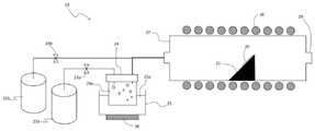
酸化剤、アミン化合物またはプロトン酸を含む有機溶媒中に、金属を溶解または分散させてなる原料溶液を霧化してミストを発生させる霧化工程と、
キャリアガスを前記ミストに供給するキャリアガス供給工程と、
前記キャリアガスによって前記ミストを前記基体へ供給するミスト供給工程と、
前記ミストを熱反応させて、前記基体表面の一部または全部に前記金属膜を積層する金属膜形成工程とを含むことを特徴とする金属膜形成方法。
[2] 前記有機溶媒が、酸化剤を含む前記[1]記載の金属膜形成方法。
[3] 前記酸化剤と前記有機溶媒との体積比が1:99〜50:50の範囲内である前記[2]記載の金属膜形成方法。
[4] 前記酸化剤が水または過酸化水素である前記[2]または[3]に記載の金属膜形成方法。
[5] 前記有機溶媒が、アミン化合物を含む前記[1]記載の金属膜形成方法。
[6] 前記アミン化合物が、ジアミンである前記[5]記載の金属膜形成方法。
[7] 前記有機溶媒が、プロトン酸を含む前記[1]記載の金属膜形成方法。
[8] 前記プロトン酸が、ハロゲン化水素酸である前記[7]記載の金属膜形成方法。
[9] 前記熱反応を、200℃〜650℃の温度で行う前記[1]〜[8]のいずれかに記載の金属膜形成方法。
[10] 前記熱反応を、不活性ガスまたは還元ガスの雰囲気下で行う前記[1]〜[9]のいずれかに記載の金属膜形成方法。
[11] 前記金属が、金(Au)、銀(Ag)、白金(Pt)、銅(Cu)、鉄(Fe)、マンガン(Mn)、ニッケル(Ni)、パラジウム(Pd)、コバルト(Co)、ロジウム(Rh)、ルテニウム(Ru)、クロム(Cr)、モリブデン(Mo)、タングステン(W)およびアルミニウム(Al)から選ばれる1種または2種以上の金属である前記[1]〜[10]のいずれかに記載の金属膜形成方法。
[12] 前記有機溶媒がアルコールである前記[1]〜[11]のいずれかに記載の金属膜形成方法。
[13] 前記原料溶液が、酸化剤、アミン化合物またはプロトン酸を含む有機溶媒と、前記金属を含む金属錯体溶液または金属塩溶液との混合溶液である前記[1]〜[12]のいずれかに記載の金属膜形成方法。
[14] 前記[1]〜[13]のいずれかに記載の金属膜形成方法を用いて形成された金属膜。
[15] 電極である前記[14]記載の金属膜。
[16] 前記[15]記載の金属膜を電極として備え、さらに半導体層を少なくとも備えている半導体装置。
That is, the present invention relates to the following invention.
[1] A metal film forming method for forming a metal film on a substrate.
An atomization step in which a raw material solution obtained by dissolving or dispersing a metal in an organic solvent containing an oxidizing agent, an amine compound or a protonic acid is atomized to generate mist.
The carrier gas supply process for supplying the carrier gas to the mist, and
A mist supply step of supplying the mist to the substrate by the carrier gas, and
A metal film forming method comprising a metal film forming step of laminating the metal film on a part or all of the surface of the substrate by thermally reacting the mist.
[2] The method for forming a metal film according to the above [1], wherein the organic solvent contains an oxidizing agent.
[3] The metal film forming method according to the above [2], wherein the volume ratio of the oxidizing agent to the organic solvent is in the range of 1:99 to 50:50.
[4] The method for forming a metal film according to the above [2] or [3], wherein the oxidizing agent is water or hydrogen peroxide.
[5] The method for forming a metal film according to the above [1], wherein the organic solvent contains an amine compound.
[6] The method for forming a metal film according to the above [5], wherein the amine compound is a diamine.
[7] The method for forming a metal film according to the above [1], wherein the organic solvent contains a protonic acid.
[8] The method for forming a metal film according to the above [7], wherein the protonic acid is a hydrohalic acid.
[9] The metal film forming method according to any one of [1] to [8], wherein the thermal reaction is carried out at a temperature of 200 ° C. to 650 ° C.
[10] The method for forming a metal film according to any one of [1] to [9], wherein the thermal reaction is carried out in an atmosphere of an inert gas or a reducing gas.
[11] The metal is gold (Au), silver (Ag), platinum (Pt), copper (Cu), iron (Fe), manganese (Mn), nickel (Ni), palladium (Pd), cobalt (Co). ), Rhodium (Rh), Ruthenium (Ru), Chromium (Cr), Molybdenum (Mo), Tungsten (W) and Aluminum (Al). 10] The metal film forming method according to any one of.
[12] The method for forming a metal film according to any one of the above [1] to [11], wherein the organic solvent is alcohol.
[13] Any of the above [1] to [12], wherein the raw material solution is a mixed solution of an organic solvent containing an oxidizing agent, an amine compound or a protonic acid and a metal complex solution or a metal salt solution containing the metal. The metal film forming method according to.
[14] A metal film formed by using the metal film forming method according to any one of [1] to [13] above.
[15] The metal film according to the above [14], which is an electrode.
[16] A semiconductor device comprising the metal film according to the above [15] as an electrode and further provided with at least a semiconductor layer .
本発明の金属膜形成方法によれば、密着性に優れた金属膜を工業的有利に成膜できる。また、本発明の金属膜は密着性に優れている。 According to the metal film forming method of the present invention, a metal film having excellent adhesion can be formed in an industrially advantageous manner. Further, the metal film of the present invention has excellent adhesion.
本発明の金属膜形成方法は、基体上に金属膜を形成する金属膜形成方法であって、酸化剤、アミン化合物またはプロトン酸を含む有機溶媒中に、金属を溶解または分散させてなる原料溶液を霧化してミストを発生させる霧化工程と、キャリアガスを前記ミストに供給するキャリアガス供給工程と、前記キャリアガスによって前記ミストを前記基体へ供給するミスト供給工程と、前記ミストを熱反応させて、前記基体表面の一部または全部に前記金属膜を積層する金属膜形成工程とを含むことを特徴とする。 The metal film forming method of the present invention is a metal film forming method for forming a metal film on a substrate, and is a raw material solution obtained by dissolving or dispersing a metal in an organic solvent containing an oxidizing agent, an amine compound or a protonic acid. An atomization step of atomizing to generate mist, a carrier gas supply step of supplying a carrier gas to the mist, a mist supply step of supplying the mist to the substrate by the carrier gas, and a thermal reaction of the mist. It is characterized by including a metal film forming step of laminating the metal film on a part or all of the surface of the substrate.
前記霧化工程は、酸化剤、アミン化合物またはプロトン酸を含む有機溶媒中に、金属を溶解または分散させて原料溶液を調整し、前記原料溶液を霧化してミストを発生させる。 In the atomization step, a metal is dissolved or dispersed in an organic solvent containing an oxidizing agent, an amine compound or a protonic acid to prepare a raw material solution, and the raw material solution is atomized to generate mist.
本工程で用いられる酸化剤を含む有機溶媒(以下、「酸化剤含有有機溶媒」ともいう)は、有機溶媒中に酸化剤を含んでいれば特に限定されず、例えば、公知の有機溶媒と酸化剤とを混合することにより得られる。前記酸化剤と前記有機溶媒との体積比は、1:99〜50:50の範囲内であるのが好ましく、1:99〜40:60の範囲内であるのがより好ましく、1:99〜10:90の範囲内であるのがさらにより好ましく、1:99〜5:95の範囲内であるのが最も好ましい。このような好ましい範囲とすることで、ミストが成膜により適したものになり、かつ膜質もより良好なものとすることができる。 The organic solvent containing an oxidizing agent used in this step (hereinafter, also referred to as “oxidizing agent-containing organic solvent”) is not particularly limited as long as the organic solvent contains an oxidizing agent, and for example, oxidation with a known organic solvent. Obtained by mixing with an agent. The volume ratio of the oxidizing agent to the organic solvent is preferably in the range of 1:99 to 50:50, more preferably in the range of 1:99 to 40:60, and is preferably in the range of 1:99 to 40:60. It is even more preferably in the range of 10:90, most preferably in the range of 1:99 to 5:95. By setting such a preferable range, the mist can be made more suitable for film formation and the film quality can be made better.
前記酸化剤としては、例えば、水、水溶性または非水溶性の公知の酸化剤などが挙げられるが、本発明においては、前記酸化剤が水または水溶性の酸化剤であるのが好ましく、水または過酸化水素であるのがより好ましく、水であるのが最も好ましい。また、前記酸化剤として、水溶性の酸化剤を用いる場合には、水と混合して水溶液の形態(例えば過酸化水素水等)で用いるのが好ましい。 Examples of the oxidizing agent include water and known water-soluble or water-insoluble oxidizing agents. In the present invention, the oxidizing agent is preferably water or a water-soluble oxidizing agent, and water. Alternatively, hydrogen peroxide is more preferable, and water is most preferable. When a water-soluble oxidizing agent is used as the oxidizing agent, it is preferable to mix it with water and use it in the form of an aqueous solution (for example, hydrogen peroxide solution).
前記酸化剤としては、より具体的には、例えば、水、過酸化水素(H2O2)、過酸化ナトリウム(Na2O2)、過酸化バリウム(BaO2)、過酸化ベンゾイル(C6H5CO)2O2等の過酸化物、次亜塩素酸(HClO)、過塩素酸、硝酸、過酢酸やニトロベンゼン等の有機過酸化物などが挙げられる。 More specifically, the oxidizing agent includes, for example, water, hydrogen peroxide (H 2 O 2 ), sodium peroxide (Na 2 O 2 ), barium peroxide (BaO 2 ), and benzoyl peroxide (C 6). Examples thereof include peroxides such as H 5 CO) 2 O 2 and organic peroxides such as hypochlorous acid (HClO), perchloric acid, nitric acid, peracetic acid and nitrobenzene.
前記水としては、より具体的には、例えば、純水、超純水、水道水、井戸水、鉱泉水、鉱水、温泉水、湧水、淡水、海水などが挙げられ、これらの水に、例えば精製、加熱、殺菌、ろ過、イオン交換、電解、浸透圧の調整、緩衝化等の処理をした水(例えば、オゾン水、精製水、熱水、イオン交換水、生理食塩水、リン酸緩衝液、リン酸緩衝生理食塩水等)も例として含まれる。 More specifically, the water includes pure water, ultra-pure water, tap water, well water, mineral spring water, mineral water, hot spring water, spring water, fresh water, seawater, and the like. Purified, heated, sterilized, filtered, ion exchange, electrolysis, osmotic pressure adjustment, buffered water (eg ozone water, purified water, hot water, ion exchange water, physiological saline, phosphate buffer) , Phosphorus buffered physiological saline, etc.) is also included as an example.
前記有機溶媒は、本発明の目的を阻害しない限り、特に限定されず、このような溶媒としては、例えば、アルコール(例、メタノール、エタノール、プロパノール、イソプロパノール、ブタノール、tert−ブタノール等)、エーテル(例、ジオキサン、テトラヒドロフラン、ジエチルエーテル、tert−ブチルメチルエーテル、ジイソプロピルエーテル、エチレングリコール−ジメチルエーテル等)、エステル(例、ギ酸エチル、酢酸エチル、酢酸n−ブチル等)、カルボン酸(例、ギ酸、酢酸、プロピオン酸等)、ハロゲン化炭化水素類(例、ジクロロメタン、クロロホルム、四塩化炭素、トリクロロエチレン、1,2−ジクロロエタン、クロロベンゼン等)、炭化水素(例、n−ヘキサン、ベンゼン、トルエン等)、アミド(例、ホルムアミド、N,N−ジメチルホルムアミド、N,N−ジメチルアセトアミド等)、ケトン(例、アセトン、メチルエチルケトン、メチルイソブチルケトン等)、ニトリル類(例、アセトニトリル、プロピオニトリル等)、スルホラン、ヘキサメチルホスホルアミド等の単独またはこれらの混合溶媒などが挙げられる。本発明においては、前記有機溶媒が、アルコール、ケトンまたはこれらの混合溶媒であるのが好ましく、アルコールであるのがより好ましく、低級アルコール(好ましくはC1〜3)であるのが最も好ましい。 The organic solvent is not particularly limited as long as the object of the present invention is not impaired, and such a solvent includes, for example, alcohol (eg, methanol, ethanol, propanol, isopropanol, butanol, tert-butanol, etc.), ether (eg, methanol, ethanol, propanol, isopropanol, butanol, tert-butanol, etc.). Examples, dioxane, tetrahydrofuran, diethyl ether, tert-butyl methyl ether, diisopropyl ether, ethylene glycol-dimethyl ether, etc.), esters (eg, ethyl formate, ethyl acetate, n-butyl acetate, etc.), carboxylic acids (eg, formate, acetate). , Propionic acid, etc.), halogenated hydrocarbons (eg, dichloromethane, chloroform, carbon tetrachloride, trichloroethylene, 1,2-dichloroethane, chlorobenzene, etc.), hydrocarbons (eg, n-hexane, benzene, toluene, etc.), amides (Example, formamide, N, N-dimethylformamide, N, N-dimethylacetamide, etc.), ketones (eg, acetone, methyl ethyl ketone, methyl isobutyl ketone, etc.), nitriles (eg, acetonitrile, propionitrile, etc.), sulfolanes, Examples thereof include a single solvent such as hexamethylphosphoramide or a mixed solvent thereof. In the present invention, the organic solvent is preferably an alcohol, a ketone or a mixed solvent thereof, more preferably an alcohol, and most preferably a lower alcohol (preferably C1 to 3).
本工程で用いられるアミン化合物を含む有機溶媒(以下、「アミン化合物含有有機溶媒」ともいう)は、有機溶媒中にアミン化合物を含んでいれば特に限定されず、例えば、公知の有機溶媒とアミン化合物とを混合することにより得られる。前記アミン化合物と前記有機溶媒との配合割合は、前記有機溶媒中、前記アミン化合物が0.001モル/L〜10モル/Lの範囲内であるのが好ましく、0.005モル/L〜1モル/Lの範囲内であるのがより好ましく、0.01モル/L〜0.1モル/Lの範囲内であるのが最も好ましい。このような好ましい範囲とすることで、ミストが成膜により適したものになり、かつ膜質もより良好なものとすることができる。 The organic solvent containing an amine compound used in this step (hereinafter, also referred to as "amine compound-containing organic solvent") is not particularly limited as long as the amine compound is contained in the organic solvent, and for example, known organic solvents and amines. Obtained by mixing with a compound. The blending ratio of the amine compound and the organic solvent is preferably in the range of 0.001 mol / L to 10 mol / L of the amine compound in the organic solvent, and 0.005 mol / L to 1 It is more preferably in the range of mol / L, and most preferably in the range of 0.01 mol / L to 0.1 mol / L. By setting such a preferable range, the mist can be made more suitable for film formation and the film quality can be made better.
前記アミン化合物は、本発明の目的を阻害しない限り特に限定されず、酸素原子、硫黄原子、窒素原子等を含んだ化合物であってもよい。前記アミン化合物としては、例えば、メチルアミン、エチルアミン、プロピルアミン、イソプロピルアミン、n−ブチルアミン、イソブチルアミン、sec−ブチルアミン、t−ブチルアミン、ヘキシルアミン、2−メトキシエチルアミン、2−エトキシエチルアミン、3−メトキシプロピルアミン、3−メチルチオプロピルアミン、エチレンジアミン、プロピレンジアミン、ブチレンジアミン、ヘキサメチレンジアミン、ジエチレントリアミン、トリエチレンテトラミン、テトラエチレンペンタミン、イミノビスプロピルアミン、メチルイミノビスプロピルアミン、ラウリルイミノビスプロピルアミン、N,N’−ビスアミノプロピル−1,3−プロピレンジアミン、N,N’−ビスアミノプロピル−1,3−ブチレンジアミン、1,2−ジアミノプロパン、ビス−(3−アミノプロピル)エーテル、ビス−(3−アミノプロポキシ)エタン、1,3ビス−(3−アミノプロポキシ)−2,2−ジメチルプロパン、N−ラウリルプロピレンジアミン、N,N’−ジ−t−ブチルエチレンジアミン、N−メチルエチレンジアミン、N−エチルエチレンジアミン、N,N−ジメチルエチレンジアミン、アリルアミン等のC1〜C16の炭素数を有する脂肪族化合物;シクロペンチルアミン、シクロヘキシルアミン、シクロヘプチルアミン、シクロオクチルアミン、アミノメチルシクロヘキサン、4−メチルシクロヘキシルアミン、1−シクロヘキシルエチルアミン、3,3,5−トリメチルシクロヘキシルアミン、イソホロンジアミン、ビスアミノメチルシクロへキサン等のC1〜C16の炭素数を有する脂環式化合物;ベンジルアミン、フェネチルアミン、4−メチルベンジルアミン、N−アミノプロピルアニリン、2−アミノ−1,2−ジフェニルエタノール、9−アミノフルオレン、ベンズヒドリルアミン、キシリレンジアミン、フェニレンジアミン、ジアミノジフェニルメタン、N−ベンジルエチレンジアミン、2−アミノピリジン、3−アミノピリジン、4−アミノピリジン、2,3−ジアミノピリジン、2,5−ジアミノピリジン、2,3,6−トリアミノピリジン、N−アミノプロピルアニリン、2−アミノ−3−メチルピリジン、2−アミノ−4−メチルピリジン、2−アミノ−6−メチルピリジン、2−アミノ−3−エチルピリジン、2−アミノ−3−プロピルピリジン、2−アミノ−4,6−ジメチルピリジン、2,6−ジアミノ−4−メチルピリジン、3−アミノ−6−イソプロピルピリジン、2,6−ジアミノピリジン等のC1〜C16の炭素数を有する芳香族化合物;ピペラジン、N−アミノプロピルピペラジン、2−メチルピペラジン、2,6−ジメチルピペラジン、2,5−ジメチルピペラジン、3−メチルアミノピペリジン、2−アミノメチルピペラジン、3−アミノピロリジン、ホモピペラジン、N−アミノプロピルピペラジン、1,4−(ビスアミノプロピル)ピペラジン、N−アミノエチルピペリジン、N−アミノプロピルピペリジン、2−アミノメチルピペリジン、4−アミノメチルピペリジン、フルフリルアミン、テトラヒドロフルフリルアミン、3−(メチルアミノ)ピロリジン、5−メチルフルフリルアミン、2−(フルフリルチオ)エチルアミン、2−ピコリルアミン、3−ピコリルアミン、4−ピコリルアミン等のC1〜C16の炭素数を有する複素環式化合物;2−ヒドロキシエチルアミン、メチル(2−ヒドロキシエチル)アミン、1−アミノ−2−プロパノール、3−アミノ−1−プロパノール、2−アミノ−1−プロパノール、1−アミノ−2−プロパノール、ジエタノールアミン、3−アミノ−1,2−プロパンジオール、2−(2−アミノエトキシ)エタノール、N−(2−ヒドロキシエチル)エチレンジアミン、2−アミノ−1,3−プロパンジオール等の水酸基を1個以上有する化合物等が挙げられる。本発明においては、前記アミン化合物がポリアミンであるのが好ましく、ジアミンであるのがより好ましい。なお、前記ポリアミンとしては、例えば、エチレンジアミン、ジエチレントリアミン、トリエチレンテトラミン、テトラエチレンペンタミン、ポリオキシプロピレンジアミン、ポリオキシプロピレントリアミン等の脂肪族ポリアミン;イソホロンジアミン、メンセンジアミン、ビス(4−アミノ−3−メチルジシクロヘキシル)メタン、ジアミノジシクロヘキシルメタン、ビス(アミノメチル)シクロヘキサン、N−アミノエチルピペラジン、3,9−ビス(3−アミノプロピル)−2,4,8,10−テトラオキサスピロ(5.5)ウンデカン等の脂環式ポリアミン;m−フェニレンジアミン、p−フェニレンジアミン、トリレン−2,4−ジアミン、トリレン−2,6−ジアミン、メシチレン−2,4−ジアミン、メシチレン−2,6−ジアミン、3,5−ジエチルトリレン−2,4−ジアミン、3,5−ジエチルトリレン−2,6−ジアミン等の単核ポリアミン;ビフェニレンジアミン、4,4−ジアミノジフェニルメタン、2,5−ナフチレンジアミン、2,6−ナフチレンジアミン等の芳香族ポリアミン;2−アミノプロピルイミダゾール等のイミダゾール等が挙げられる。 The amine compound is not particularly limited as long as it does not interfere with the object of the present invention, and may be a compound containing an oxygen atom, a sulfur atom, a nitrogen atom and the like. Examples of the amine compound include methylamine, ethylamine, propylamine, isopropylamine, n-butylamine, isobutylamine, sec-butylamine, t-butylamine, hexylamine, 2-methoxyethylamine, 2-ethoxyethylamine and 3-methoxy. Propylamine, 3-methylthiopropylamine, ethylenediamine, propylenediamine, butylenediamine, hexamethylenediamine, diethylenetriamine, triethylenetetramine, tetraethylenepentamine, iminobispropylamine, methyliminobispropylamine, lauryliminobispropylamine, N , N'-bisaminopropyl-1,3-propylenediamine, N, N'-bisaminopropyl-1,3-butylenediamine, 1,2-diaminopropane, bis- (3-aminopropyl) ether, bis- (3-Aminopropoxy) ethane, 1,3 bis- (3-aminopropoxy) -2,2-dimethylpropane, N-laurylpropylenediamine, N, N'-di-t-butylethylenediamine, N-methylethylenediamine, An aliphatic compound having C1 to C16 carbon atoms such as N-ethylethylenediamine, N, N-dimethylethylenediamine, and allylamine; cyclopentylamine, cyclohexylamine, cycloheptylamine, cyclooctylamine, aminomethylcyclohexane, 4-methylcyclohexylamine. , 1-Cyclohexylethylamine, 3,3,5-trimethylcyclohexylamine, isophoronediamine, bisaminomethylcyclohexane and other alicyclic compounds having C1-C16 carbon atoms; benzylamine, phenethylamine, 4-methylbenzylamine , N-aminopropylaniline, 2-amino-1,2-diphenylethanol, 9-aminofluorene, benzhydrylamine, xylylene diamine, phenylenediamine, diaminodiphenylmethane, N-benzylethylenediamine, 2-aminopyridine, 3-amino Pyridine, 4-aminopyridine, 2,3-diaminopyridine, 2,5-diaminopyridine, 2,3,6-triaminopyridine, N-aminopropylaniline, 2-amino-3-methylpyridine, 2-amino- 4-Methylpyridine, 2-amino-6-methylpyridine, 2-amino-3-ethylpyridine, 2-amino-3-propylpyridine, 2-amino-4,6-dimethylpi Aromatic compounds having C1-C16 carbon atoms such as lysine, 2,6-diamino-4-methylpyridine, 3-amino-6-isopropylpyridine, 2,6-diaminopyridine; piperazine, N-aminopropyl piperazine, 2-Methylpiperazin, 2,6-dimethylpiperazin, 2,5-dimethylpiperazin, 3-methylaminopiperidin, 2-aminomethylpiperazine, 3-aminopyrrolidin, homopiperazin, N-aminopropylpiperazin, 1,4-( Bisaminopropyl) piperazine, N-aminoethyl piperidine, N-aminopropyl piperidine, 2-aminomethyl piperidine, 4-aminomethyl piperidine, furfurylamine, tetrahydrofurfurylamine, 3- (methylamino) pyrrolidine, 5-methylfurfurylamine , 2- (Fulfurylthio) ethylamine, 2-picorylamine, 3-picorylamine, 4-picorylamine and other heterocyclic compounds having C1-C16 carbon atoms; 2-hydroxyethylamine, methyl (2-hydroxyethyl) amine , 1-amino-2-propanol, 3-amino-1-propanol, 2-amino-1-propanol, 1-amino-2-propanol, diethanolamine, 3-amino-1,2-propanediol, 2- (2) Examples thereof include compounds having one or more hydroxyl groups such as −aminoethoxy) ethanol, N- (2-hydroxyethyl) ethylenediamine, and 2-amino-1,3-propanediol. In the present invention, the amine compound is preferably a polyamine, more preferably a diamine. Examples of the polyamine include aliphatic polyamines such as ethylenediamine, diethylenetriamine, triethylenetetramine, tetraethylenepentamine, polyoxypropylenediamine, and polyoxypropylenetriamine; isophoronediamine, mensendiamine, and bis (4-amino-). 3-Methyldicyclohexyl) methane, diaminodicyclohexylmethane, bis (aminomethyl) cyclohexane, N-aminoethylpiperazine, 3,9-bis (3-aminopropyl) -2,4,8,10-tetraoxaspiro (5. 5) Alicyclic polyamines such as undecane; m-phenylenediamine, p-phenylenediamine, trilen-2,4-diamine, trilen-2,6-diamine, mesitylen-2,4-diamine, mesitylen-2,6- Mononuclear polyamines such as diamine, 3,5-diethyltrilen-2,4-diamine, 3,5-diethyltrilen-2,6-diamine; biphenylenediamine, 4,4-diaminodiphenylmethane, 2,5-naphthic Aromatic polyamines such as diamines and 2,6-naphthylenediamines; imidazoles such as 2-aminopropyl imidazole and the like can be mentioned.
アミン化合物含有有機溶媒に用いられる有機溶媒は、本発明の目的を阻害しない限り、特に限定されず、このような溶媒としては、例えば、アルコール(例、メタノール、エタノール、プロパノール、イソプロパノール、ブタノール、tert−ブタノール等)、エーテル(例、ジオキサン、テトラヒドロフラン、ジエチルエーテル、tert−ブチルメチルエーテル、ジイソプロピルエーテル、エチレングリコール−ジメチルエーテル等)、エステル(例、ギ酸エチル、酢酸エチル、酢酸n−ブチル等)、カルボン酸(例、ギ酸、酢酸、プロピオン酸等)、ハロゲン化炭化水素類(例、ジクロロメタン、クロロホルム、四塩化炭素、トリクロロエチレン、1,2−ジクロロエタン、クロロベンゼン等)、炭化水素(例、n−ヘキサン、ベンゼン、トルエン等)、ケトン(例、アセトン、メチルエチルケトン、メチルイソブチルケトン等)等の単独またはこれらの混合溶媒などが挙げられる。本発明においては、前記有機溶媒が、アルコール、ケトンまたはこれらの混合溶媒であるのが好ましく、アルコールであるのがより好ましく、低級アルコール(好ましくはC1〜3)であるのが最も好ましい。 The organic solvent used for the amine compound-containing organic solvent is not particularly limited as long as the object of the present invention is not impaired, and examples of such a solvent include alcohols (eg, methanol, ethanol, propanol, isopropanol, butanol, tert). -Butanol etc.), ethers (eg dioxane, tetrahydrofuran, diethyl ether, tert-butyl methyl ether, diisopropyl ether, ethylene glycol-dimethyl ether etc.), esters (eg ethyl formate, ethyl acetate, n-butyl acetate etc.), carboxylic Acids (eg, formic acid, acetic acid, propionic acid, etc.), halogenated hydrocarbons (eg, dichloromethane, chloroform, carbon tetrachloride, trichloroethylene, 1,2-dichloroethane, chlorobenzene, etc.), hydrocarbons (eg, n-hexane, etc.) Examples thereof include a single solvent such as benzene (benzene, toluene, etc.), a ketone (eg, acetone, methyl ethyl ketone, methyl isobutyl ketone, etc.) or a mixed solvent thereof. In the present invention, the organic solvent is preferably an alcohol, a ketone or a mixed solvent thereof, more preferably an alcohol, and most preferably a lower alcohol (preferably C1 to 3).
本工程で用いられるプロトン酸を含む有機溶媒(以下、「プロトン酸含有有機溶媒」ともいう)は、有機溶媒中にプロトン酸を含んでいれば特に限定されず、例えば、公知の有機溶媒とプロトン酸とを混合することにより得られる。前記プロトン酸と前記有機溶媒との配合割合は、前記有機溶媒中、前記プロトン酸が0.001モル/L〜10モル/Lの範囲内であるのが好ましく、0.005モル/L〜1モル/Lの範囲内であるのがより好ましく、0.01モル/L〜0.1モル/Lの範囲内であるのが最も好ましい。このような好ましい範囲とすることで、ミストが成膜により適したものになり、かつ膜質もより良好なものとすることができる。 The organic solvent containing a protonic acid used in this step (hereinafter, also referred to as “proton acid-containing organic solvent”) is not particularly limited as long as the organic solvent contains a protonic acid, and for example, a known organic solvent and protons. Obtained by mixing with an acid. The mixing ratio of the protonic acid and the organic solvent is preferably in the range of 0.001 mol / L to 10 mol / L of the protonic acid in the organic solvent, and 0.005 mol / L to 1 It is more preferably in the range of mol / L, and most preferably in the range of 0.01 mol / L to 0.1 mol / L. By setting such a preferable range, the mist can be made more suitable for film formation and the film quality can be made better.
前記プロトン酸は、本発明の目的を阻害しない限り特に限定されず、公知のものであってよい。前記プロトン酸としては、例えば、塩酸、硫酸、硝酸、リン酸、ホウフッ化水素酸、フッ化水素酸、過塩素酸等の無機酸や、有機カルボン酸、フェノール類、有機スルホン酸等が挙げられる。さらに、有機カルボン酸としては、例えば、ギ酸、酢酸、ショウ酸、安息香酸、フタル酸、マレイン酸、フマル酸、マロン酸、酒石酸、クエン酸、乳酸、コハク酸、モノクロロ酢酸、ジクロロ酢酸、トリクロロ酢酸、トリフルオロ酢酸、ニトロ酢酸、トリフェニル酢酸等が挙げられる。有機スルホン酸としては、例えば、アルキルベンゼンスルホン酸、アルキルナフタレンスルホン酸、アルキルナフタレンジスルホン酸、ナフタレンスルホン酸ホルマリン重縮合物、メラミンスルホン酸ホルマリン重縮合物、ナフタレンジスルホン酸、ナフタレントリスルホン酸、ジナフチルメタンジスルホン酸、アントラキノンスルホン酸、アントラキノンジスルホン酸、アントラセンスルホン酸、ピレンスルホン酸などが挙げられる。また、これらの金属塩も使用できる。本発明においては、前記プロトン酸が、無機酸であるのが好ましく、ハロゲン化水素酸であるのがより好ましい。ハロゲン化水素酸としては、例えば、塩酸、臭化水素酸、ヨウ化水素酸、フッ化水素酸などが挙げられる。 The protonic acid is not particularly limited as long as it does not interfere with the object of the present invention, and may be known. Examples of the protonic acid include inorganic acids such as hydrochloric acid, sulfuric acid, nitric acid, phosphoric acid, borofluoric acid, hydrofluoric acid and perchloric acid, organic carboxylic acids, phenols and organic sulfonic acids. .. Further, examples of the organic carboxylic acid include formic acid, acetic acid, oxalic acid, benzoic acid, phthalic acid, maleic acid, fumaric acid, malonic acid, tartaric acid, citric acid, lactic acid, succinic acid, monochloroacetic acid, dichloroacetic acid and trichloroacetic acid. , Trifluoroacetic acid, nitroacetic acid, triphenylacetic acid and the like. Examples of the organic sulfonic acid include alkylbenzene sulfonic acid, alkylnaphthalene sulfonic acid, alkylnaphthalenedisulfonic acid, naphthalenesulfonic acid formarin polycondensate, melamine sulfonic acid formarin polycondensate, naphthalenedisulfonic acid, naphthalenetrisulfonic acid and dinaphthylmethane. Examples thereof include disulfonic acid, anthraquinone sulfonic acid, anthraquinone disulfonic acid, anthracene sulfonic acid and pyrene sulfonic acid. Moreover, these metal salts can also be used. In the present invention, the protonic acid is preferably an inorganic acid, more preferably a hydrohalic acid. Examples of the hydrohalic acid include hydrochloric acid, hydrobromic acid, hydroiodic acid, hydrofluoric acid and the like.
プロトン酸含有有機溶媒に用いられる有機溶媒は、本発明の目的を阻害しない限り、特に限定されず、このような溶媒としては、例えば、アルコール(例、メタノール、エタノール、プロパノール、イソプロパノール、ブタノール、tert−ブタノール等)、エーテル(例、ジオキサン、テトラヒドロフラン、ジエチルエーテル、tert−ブチルメチルエーテル、ジイソプロピルエーテル、エチレングリコール−ジメチルエーテル等)、エステル(例、ギ酸エチル、酢酸エチル、酢酸n−ブチル等)、ケトン(例、アセトン、メチルエチルケトン、メチルイソブチルケトン等)等の単独またはこれらの混合溶媒などが挙げられる。本発明においては、前記有機溶媒が、アルコール、ケトンまたはこれらの混合溶媒であるのが好ましく、アルコールであるのがより好ましく、低級アルコール(好ましくはC1〜3)であるのが最も好ましい。 The organic solvent used for the protonic acid-containing organic solvent is not particularly limited as long as the object of the present invention is not impaired, and examples of such a solvent include alcohols (eg, methanol, ethanol, propanol, isopropanol, butanol, tert). -Butanol etc.), ethers (eg dioxane, tetrahydrofuran, diethyl ether, tert-butyl methyl ether, diisopropyl ether, ethylene glycol-dimethyl ether etc.), esters (eg ethyl formate, ethyl acetate, n-butyl acetate etc.), ketones (Example, acetone, methyl ethyl ketone, methyl isobutyl ketone, etc.) and the like alone or a mixed solvent thereof and the like can be mentioned. In the present invention, the organic solvent is preferably an alcohol, a ketone or a mixed solvent thereof, more preferably an alcohol, and most preferably a lower alcohol (preferably C1 to 3).
本工程で用いられる金属は、本発明の目的を阻害しない限り、特に限定されないが、金(Au)、銀(Ag)、白金(Pt)、銅(Cu)、鉄(Fe)、マンガン(Mn)、ニッケル(Ni)、パラジウム(Pd)、コバルト(Co)、ロジウム(Rh)、ルテニウム(Ru)、クロム(Cr)、モリブデン(Mo)、タングステン(W)およびアルミニウム(Al)から選ばれる1種または2種以上の金属であるのが好ましい。 The metal used in this step is not particularly limited as long as it does not interfere with the object of the present invention, but is not limited to gold (Au), silver (Ag), platinum (Pt), copper (Cu), iron (Fe), and manganese (Mn). ), Nickel (Ni), Palladium (Pd), Cobalt (Co), Rhodium (Rh), Ruthenium (Ru), Chromium (Cr), Molybdenum (Mo), Tungsten (W) and Aluminum (Al) 1 It is preferably a seed or two or more metals.
本工程では、前記の酸化剤含有有機溶媒中、アミン化合物含有有機溶媒中またはプロトン酸含有有機溶媒中に、前記金属を溶解または分散させて、原料溶液を調整する。前記原料溶液は、前記金属が、酸化剤含有有機溶媒中、アミン化合物含有有機溶媒中またはプロトン酸含有有機溶媒中に溶解または分散していれば特に限定されないが、本発明においては、酸化剤、アミン化合物またはプロトン酸を含む有機溶媒と、前記金属を含む金属錯体溶液または金属塩溶液との混合溶液であるのが好ましい。
前記金属の配合割合は、特に限定されないが、原料溶液全体に対して、0.01〜70質量%であるのが好ましく、0.1〜50質量であるのがより好ましい。
In this step, the metal is dissolved or dispersed in the oxidizing agent-containing organic solvent, the amine compound-containing organic solvent, or the protonic acid-containing organic solvent to prepare a raw material solution. The raw material solution is not particularly limited as long as the metal is dissolved or dispersed in an oxidizing agent-containing organic solvent, an amine compound-containing organic solvent, or a protonic acid-containing organic solvent. It is preferably a mixed solution of an organic solvent containing an amine compound or a protonic acid and a metal complex solution or a metal salt solution containing the metal.
The mixing ratio of the metal is not particularly limited, but is preferably 0.01 to 70% by mass, more preferably 0.1 to 50% by mass, based on the entire raw material solution.
酸化剤、アミン化合物またはプロトン酸を含む有機溶媒中に、金属を溶解または分散させてなる前記原料溶液は、金属膜形成用ミストの前駆体溶液として、特に有用である。 The raw material solution obtained by dissolving or dispersing a metal in an organic solvent containing an oxidizing agent, an amine compound or a protonic acid is particularly useful as a precursor solution of a mist for forming a metal film.
本工程では、前記原料溶液を霧化してミストを発生させる。霧化手段は、前記原料溶液を霧化できさえすれば特に限定されず、公知の霧化手段であってよいが、本発明においては、超音波を用いる霧化手段であるのが好ましい。 In this step, the raw material solution is atomized to generate mist. The atomizing means is not particularly limited as long as the raw material solution can be atomized, and may be a known atomizing means, but in the present invention, the atomizing means using ultrasonic waves is preferable.
前記キャリアガス供給工程では、キャリアガスを前記ミストに供給する。キャリアガスの種類としては、本発明の目的を阻害しない限り特に限定されず、例えば、酸素、窒素やアルゴン等の不活性ガス、または水素ガスやフォーミングガス等の還元ガスなどが好適な例として挙げられる。また、キャリアガスの種類は1種類であってよいが、2種類以上であってもよく、キャリアガス濃度を変化させた希釈ガス(例えば10倍希釈ガス等)などを、第2のキャリアガスとしてさらに用いてもよい。また、キャリアガスの供給箇所も1箇所だけでなく、2箇所以上あってもよい。 In the carrier gas supply step, the carrier gas is supplied to the mist. The type of carrier gas is not particularly limited as long as the object of the present invention is not impaired, and for example, an inert gas such as oxygen, nitrogen or argon, or a reducing gas such as hydrogen gas or forming gas is a preferable example. Be done. Further, the type of the carrier gas may be one type, but may be two or more types, and a diluted gas having a changed carrier gas concentration (for example, a 10-fold diluted gas) or the like is used as the second carrier gas. It may be used further. Further, the carrier gas may be supplied not only at one location but also at two or more locations.
ミスト供給工程では、前記キャリアガスによって前記ミストを基体へ供給する。キャリアガスの流量は、特に限定されないが、0.01〜20L/分であるのが好ましく、1〜10L/分であるのがより好ましい。 In the mist supply step, the mist is supplied to the substrate by the carrier gas. The flow rate of the carrier gas is not particularly limited, but is preferably 0.01 to 20 L / min, and more preferably 1 to 10 L / min.
前記基体は、金属膜を支持できるものであれば特に限定されない。前記基体の材料も、本発明の目的を阻害しない限り特に限定されず、公知の基体であってよく、有機化合物であってもよいし、無機化合物であってもよい。前記基体の形状としては、例えば、平板や円板等の板状、繊維状、棒状、円柱状、角柱状、筒状、螺旋状、球状、リング状などが挙げられるが、本発明においては、基板が好ましい。 The substrate is not particularly limited as long as it can support the metal film. The material of the substrate is not particularly limited as long as it does not impair the object of the present invention, and may be a known substrate, an organic compound, or an inorganic compound. Examples of the shape of the substrate include plate-like, fibrous, rod-like, columnar, prismatic, tubular, spiral, spherical, and ring-shaped plates such as flat plates and disks. A substrate is preferred.
前記基板は、板状であって、膜の支持体となるものであれば特に限定されない。絶縁体基板であってもよいし、半導体基板であってもよいし、導電性基板であってもよいが、前記基板が、絶縁体基板であるのが好ましく、表面に金属膜を有する基板であるのも好ましい。本発明においては、前記基板が、コランダム構造を有する結晶物を主成分として含む基板、またはβ−ガリア構造を有する結晶物を主成分として含む基板であるのも好ましい。コランダム構造を有する結晶物を主成分として含む基板は、基板中の組成比で、コランダム構造を有する結晶物を50%以上含むものであれば、特に限定されないが、本発明においては、70%以上含むものであるのが好ましく、90%以上であるのがより好ましい。コランダム構造を有する結晶を主成分とする基板としては、例えば、サファイア基板(例:c面サファイア基板)や、α型酸化ガリウム基板などが挙げられる。β−ガリア構造を有する結晶物を主成分とする基板は、基板中の組成比で、β−ガリア構造を有する結晶物を50%以上含むものであれば、特に限定されないが、本発明においては、70%以上含むものであるのが好ましく、90%以上であるのがより好ましい。β−ガリア構造を有する結晶物を主成分とする基板としては、例えばβ−Ga2O3基板、又はGa2O3とAl2O3とを含みAl2O3が0wt%より多くかつ60wt%以下である混晶体基板などが挙げられる。その他の下地基板の例としては、六方晶構造を有する基板(例:SiC基板、ZnO基板、GaN基板)などが挙げられる。六方晶構造を有する基板上には、直接または別の層(例:緩衝層)を介して、膜を形成するのが好ましい。基板の厚さは、本発明においては特に限定されないが、好ましくは、50〜2000μmであり、より好ましくは200〜800μmである。 The substrate is not particularly limited as long as it has a plate shape and serves as a support for the film. It may be an insulator substrate, a semiconductor substrate, or a conductive substrate, but the substrate is preferably an insulator substrate, and is a substrate having a metal film on the surface. It is also preferable to have it. In the present invention, it is also preferable that the substrate is a substrate containing a crystal having a corundum structure as a main component or a substrate containing a crystal having a β-gaul structure as a main component. The substrate containing a crystal having a corundum structure as a main component is not particularly limited as long as it contains 50% or more of a crystal having a corundum structure in terms of the composition ratio in the substrate, but in the present invention, it is 70% or more. It is preferably contained, and more preferably 90% or more. Examples of the substrate containing a crystal having a corundum structure as a main component include a sapphire substrate (eg, a c-plane sapphire substrate) and an α-type gallium oxide substrate. The substrate containing a crystal having a β-gaul structure as a main component is not particularly limited as long as it contains 50% or more of a crystal having a β-gaul structure in terms of the composition ratio in the substrate, but in the present invention, it is not particularly limited. , 70% or more is preferable, and 90% or more is more preferable. Examples of the substrate containing a crystal having a β-Galia structure as a main component include a β-Ga 2 O 3 substrate or a Ga 2 O 3 and Al 2 O 3 and Al 2 O 3 is more than 0 wt% and 60 wt. % Or less, such as a mixed crystal substrate. Examples of other base substrates include substrates having a hexagonal structure (eg, SiC substrate, ZnO substrate, GaN substrate) and the like. It is preferable to form a film on the substrate having a hexagonal structure directly or via another layer (eg, a buffer layer). The thickness of the substrate is not particularly limited in the present invention, but is preferably 50 to 2000 μm, and more preferably 200 to 800 μm.
金属膜形成工程では、前記ミストを熱反応させて、前記基体表面の一部または全部に前記金属膜を積層する。前記熱反応は、熱でもって前記ミストが反応すればそれでよく、反応条件等も本発明の目的を阻害しない限り特に限定されない。本工程においては、前記熱反応を、200℃〜650℃の温度で行うのが好ましく、300℃〜600℃の温度で行うのがより好ましく、400℃〜550℃の温度で行うのが最も好ましい。また、前記熱反応を、非酸素雰囲気下で行うのも好ましく、窒素ガスやアルゴンガス等の不活性ガス、またはフォーミングガスや水素ガス等の還元ガスの雰囲気下で行うのがより好ましく、不活性ガスの雰囲気下で行うのが最も好ましい。また、加圧下、減圧下、常圧下および大気圧下のいずれの条件で反応を行ってもよいが、本発明においては、常圧下または大気圧下で行うのが好ましい。なお、膜厚は成膜時間を調整することにより、設定することができるが、本発明においては、膜を厚くしても密着性に優れているので、成膜時間を長く設定するのが好ましい。好ましい成膜時間は10分間以上であり、より好ましくは30分間以上であり、最も好ましくは1時間以上である。 In the metal film forming step, the mist is thermally reacted to laminate the metal film on a part or all of the surface of the substrate. The thermal reaction may be such that the mist reacts with heat, and the reaction conditions and the like are not particularly limited as long as the object of the present invention is not impaired. In this step, the thermal reaction is preferably carried out at a temperature of 200 ° C. to 650 ° C., more preferably 300 ° C. to 600 ° C., and most preferably 400 ° C. to 550 ° C. .. Further, the thermal reaction is preferably carried out in a non-oxygen atmosphere, more preferably in an atmosphere of an inert gas such as nitrogen gas or argon gas, or a reducing gas such as forming gas or hydrogen gas, and is inert. Most preferably, it is carried out in a gas atmosphere. Further, the reaction may be carried out under any conditions of pressurization, reduced pressure, normal pressure and atmospheric pressure, but in the present invention, it is preferably carried out under normal pressure or atmospheric pressure. The film thickness can be set by adjusting the film formation time, but in the present invention, the film thickness is excellent even if the film is thickened, so it is preferable to set the film thickness longer. .. The film formation time is preferably 10 minutes or more, more preferably 30 minutes or more, and most preferably 1 hour or more.
本発明によれば、断続的に結晶成長できるためなのかどうか等は不明であるが、いずれにせよ、密着性に優れた金属膜を形成することができる。また、本発明によれば、密着性に優れたままで、膜厚200nm以上の金属膜(好ましくは膜厚300nm以上、より好ましくは500nm以上、さらにより好ましくは1μm以上、最も好ましくは10μm以上の金属膜)を容易に形成することができる。そのため、本発明の金属膜形成方法により得られた金属膜は電極やコンタクト層に有用であり、このような金属膜も本発明に含まれ、本発明の金属膜は、電極やコンタクト層として用いることができる。また、本発明の金属膜からなる電極は、半導体装置に有用であり、少なくとも半導体層とともに半導体装置に用いられる。 According to the present invention, it is unclear whether or not the crystal growth is possible intermittently, but in any case, a metal film having excellent adhesion can be formed. Further, according to the present invention, a metal film having a film thickness of 200 nm or more (preferably a metal film having a film thickness of 300 nm or more, more preferably 500 nm or more, still more preferably 1 μm or more, and most preferably 10 μm or more, while maintaining excellent adhesion. The film) can be easily formed. Therefore, the metal film obtained by the metal film forming method of the present invention is useful for an electrode or a contact layer, and such a metal film is also included in the present invention, and the metal film of the present invention is used as an electrode or a contact layer. be able to. Further, the electrode made of the metal film of the present invention is useful for a semiconductor device, and is used in a semiconductor device together with at least a semiconductor layer.
前記半導体層としては、例えば、酸化物半導体層、窒化物半導体層、ケイ素含有半導体層などが挙げられる。前記酸化物半導体層は、好ましくは、インジウム、アルミニウムおよびガリウムから選ばれる1種または2種以上の元素を含有する酸化物半導体を主成分として含む半導体層である。前記窒化物半導体層は、好ましくは、インジウム、アルミニウムおよびガリウムから選ばれる1種または2種以上の元素を含有する窒化物半導体を主成分として含む半導体層である。前記ケイ素含有半導体層は、好ましくは、ケイ素または炭化ケイ素を主成分として含む半導体層である。 Examples of the semiconductor layer include an oxide semiconductor layer, a nitride semiconductor layer, and a silicon-containing semiconductor layer. The oxide semiconductor layer is preferably a semiconductor layer containing an oxide semiconductor containing one or more elements selected from indium, aluminum and gallium as a main component. The nitride semiconductor layer is preferably a semiconductor layer containing a nitride semiconductor containing one or more elements selected from indium, aluminum and gallium as a main component. The silicon-containing semiconductor layer is preferably a semiconductor layer containing silicon or silicon carbide as a main component.
本発明の金属膜は、従来の金属膜のように種々の用途に用いることができ、例えば、電極やコンタクト層として、様々な半導体装置に有用であり、とりわけ、パワーデバイスに有用である。また、前記半導体装置は、電極が半導体層の片面側に形成された横型の素子(横型デバイス)と、半導体層の表裏両面側にそれぞれ電極を有する縦型の素子(縦型デバイス)に分類することができるが、本発明の金属膜は、横型デバイスにも縦型デバイスにも好適に用いることができる。本発明においては、前記金属膜を電極として縦型デバイスに用いることが好ましい。 The metal film of the present invention can be used for various purposes like a conventional metal film, and is useful for various semiconductor devices as an electrode or a contact layer, and is particularly useful for a power device. Further, the semiconductor device is classified into a horizontal element (horizontal device) in which electrodes are formed on one side of the semiconductor layer and a vertical element (vertical device) in which electrodes are provided on both front and back sides of the semiconductor layer. However, the metal film of the present invention can be suitably used for both horizontal devices and vertical devices. In the present invention, it is preferable to use the metal film as an electrode in a vertical device.
前記半導体装置としては、例えば、ショットキーバリアダイオード(SBD)、金属半導体電界効果トランジスタ(MESFET)、高電子移動度トランジスタ(HEMT)、金属酸化膜半導体電界効果トランジスタ(MOSFET)、静電誘導トランジスタ(SIT)、接合電界効果トランジスタ(JFET)、絶縁ゲート型バイポーラトランジスタ(IGBT)または発光ダイオードなどが挙げられる。本発明においては、前記半導体装置が、SBD、MOSFET、SIT、JFETまたはIGBTであるのが好ましく、SBD、MOSFETまたはSITであるのがより好ましい。 Examples of the semiconductor device include a Schottky barrier diode (SBD), a metal semiconductor field effect transistor (MESFET), a high electron mobility transistor (HEMT), a metal oxide film semiconductor field effect transistor (MOSFET), and an electrostatic induction transistor (MSFET). SIT), junction field effect transistor (JFET), insulated gate bipolar transistor (IGBT), light emitting diode and the like. In the present invention, the semiconductor device is preferably an SBD, MOSFET, SIT, JFET or IGBT, and more preferably an SBD, MOSFET or SIT.
なお、前記半導体装置は、さらに他の層(例えば絶縁体層、半絶縁体層、導体層、半導体層、緩衝層またはその他中間層等)などが含まれていてもよい。 The semiconductor device may further include other layers (for example, an insulator layer, a semi-insulator layer, a conductor layer, a semiconductor layer, a buffer layer, or another intermediate layer).
図1を用いて、本実施例で用いたミストエピタキシー装置19を説明する。図1のミストエピタキシー装置19は、基板20を載置するサセプタ21と、キャリアガスを供給するキャリアガス供給手段22aと、キャリアガス供給手段22aから送り出されるキャリアガスの流量を調節するための流量調節弁23aと、キャリアガス(希釈)を供給するキャリアガス(希釈)供給手段22bと、キャリアガス(希釈)供給手段22bから送り出されるキャリアガスの流量を調節するための流量調節弁23bと、原料溶液24aが収容されるミスト発生源24と、水25aが入れられる容器25と、容器25の底面に取り付けられた超音波振動子26と、内径40mmの石英管からなる供給管27と、供給管27の周辺部に設置されたヒーター28を備えている。サセプタ21は、石英からなり、基板20を載置する面が水平面から傾斜している。成膜室となる供給管27とサセプタ21をどちらも石英で作製することにより、基板20上に形成される膜内に装置由来の不純物が混入することを抑制している。
The
原料溶液として、ロジウムアセチルアセトナート(0.01mol/L)を、メタノールと水との混合溶媒(メタノール:水=9.5:0.5)に入れて分散させた溶液を用いた。基板として、c面サファイアを用いた。キャリアガスとして、窒素を用いた。キャリアガスの流量は、5L/分とし、キャリアガス(希釈)の流量は、0.5L/分に設定した。成膜は、窒素雰囲気下500℃で行った。
得られた金属膜につき、ロジウム金属膜が形成されていることを、X線回折装置を用いて確認した。また、得られたロジウム膜につき、断面SEMでもって、膜厚を測定した。その結果、約11.7μmであった。なお、この断面SEM像を図2に示す。
また、SEMを用いて、金属膜表面を観察した。その結果、凸凹が少なく、きれいな表面を有していた。なお、この金属膜表面のSEM像を図3に示す。
また、密着性につき、応力を加えて、目視により、剥離状況を観察したが、剥離等は全く生じず、密着性も優れていた。
As a raw material solution, a solution in which rhodium acetylacetonate (0.01 mol / L) was placed in a mixed solvent of methanol and water (methanol: water = 9.5: 0.5) and dispersed was used. A c-plane sapphire was used as the substrate. Nitrogen was used as the carrier gas. The flow rate of the carrier gas was set to 5 L / min, and the flow rate of the carrier gas (dilution) was set to 0.5 L / min. The film formation was performed at 500 ° C. in a nitrogen atmosphere.
It was confirmed by using an X-ray diffractometer that a rhodium metal film was formed on the obtained metal film. In addition, the film thickness of the obtained rhodium film was measured with a cross-sectional SEM. As a result, it was about 11.7 μm. The cross-sectional SEM image is shown in FIG.
In addition, the surface of the metal film was observed using SEM. As a result, it had a clean surface with few irregularities. The SEM image of the surface of the metal film is shown in FIG.
Further, regarding the adhesion, stress was applied and the peeling state was visually observed, but peeling and the like did not occur at all, and the adhesion was also excellent.
水とメタノールの配合割合(体積比)を表1に示す比率としたこと以外は実施例1と同様に金属膜を成膜し、その成膜状態を観察し、さらに、密着性を評価した。結果を表1に示す。 A metal film was formed in the same manner as in Example 1 except that the mixing ratio (volume ratio) of water and methanol was set to the ratio shown in Table 1, the film formation state was observed, and the adhesion was further evaluated. The results are shown in Table 1.

ロジウムアセチルアセトナートに代えてアルミニウムアセチルアセトナートを用いたこと以外、実施例1と同様にして金属膜を成膜した。アルミニウムでもロジウムの場合と同様に成膜できることが分かった。 A metal film was formed in the same manner as in Example 1 except that aluminum acetylacetonate was used instead of rhodium acetylacetonate. It was found that aluminum can also form a film in the same manner as rhodium.
1.成膜装置
実施例4では、実施例1で用いたミストエピタキシー装置19に代えて、図4に示すミストエピタキシー装置1を用いた。以下、図4を用いて、実施例4で用いたミストCVD装置1を説明する。ミストCVD装置1は、キャリアガスを供給するキャリアガス源2aと、キャリアガス源2aから送り出されるキャリアガスの流量を調節するための流量調節弁3aと、キャリアガス(希釈)を供給するキャリアガス(希釈)源2bと、キャリアガス(希釈)源2bから送り出されるキャリアガス(希釈)の流量を調節するための流量調節弁3bと、原料溶液4aが収容されるミスト発生源4と、水5aが入れられる容器5と、容器5の底面に取り付けられた超音波振動子6と、成膜室7と、ミスト発生源4から成膜室7までをつなぐ供給管9と、成膜室7内に設置されたホットプレート8と、熱反応後のミスト、液滴および排気ガスを排出する排気口11とを備えている。なお、ホットプレート8上には、基板10が設置されている。
1. 1. In the film forming apparatus Example 4, the mist epitaxy apparatus 1 shown in FIG. 4 was used instead of the
2.原料溶液の作製
銅アセチルアセトナートが0.05モル/Lとなるように、メタノールに銅アセチルアセトナートを混合し、さらに、キレート剤として、エチレンジアミンを混合溶液中0.5体積%となるように添加し、原料溶液4aを調製した。
2. Preparation of raw material solution Copper acetylacetonate is mixed with methanol so that the amount of copper acetylacetonate is 0.05 mol / L, and ethylenediamine as a chelating agent is added to 0.5% by volume in the mixed solution. Addition was made to prepare a
3.成膜準備
上記2.で得られた原料溶液4aをミスト発生源4内に収容した。次に、基板10としてガラス基板を用いて、ガラス基板をホットプレート8上に設置し、ホットプレート8を作動させて成膜室7内の温度を500℃にまで昇温させた。次に、流量調節弁3a、3bを開いて、キャリアガス源であるキャリアガス供給手段2a、2bからキャリアガスを成膜室7内に供給し、成膜室7の雰囲気をキャリアガスで十分に置換した後、キャリアガスの流量を5.0L/分に、キャリアガス(希釈)の流量を0.5L/分にそれぞれ調節した。なお、キャリアガスとして窒素を用いた。
3. 3. Preparation for film formation 2. The
4.金属膜の形成
次に、超音波振動子6を2.4MHzで振動させ、その振動を、水5aを通じて原料溶液4aに伝播させることによって、原料溶液4aを霧化させてミスト4bを生成させた。このミスト4bが、キャリアガスによって、供給管9内を通って、成膜室7内に導入され、大気圧下、400℃にて、成膜室7内でミストが熱反応して、基板10上に銅膜が形成された。成膜時間は30分間であった。銅膜については、X線測定装置を用いて確認した。XRD測定結果を図5に示す。なお、膜厚は200nmであった。また、実施例1と同様にして、密着性を評価したところ、良好であった。
4. Formation of metal film Next, the
成膜温度を400℃に代えて500℃にしたこと以外は、実施例4と同様にして銅膜を得た。銅膜については、X線測定装置を用いて確認した。XRD測定結果を図6に示す。なお、膜厚は925nmであった。また、実施例1と同様にして、密着性を評価したところ、良好であった。 A copper film was obtained in the same manner as in Example 4 except that the film formation temperature was set to 500 ° C. instead of 400 ° C. The copper film was confirmed using an X-ray measuring device. The XRD measurement result is shown in FIG. The film thickness was 925 nm. Moreover, when the adhesion was evaluated in the same manner as in Example 1, it was good.
銅アセチルアセトナートが0.05モル/Lとなるように、メタノールに銅アセチルアセトナートを混合し、さらに、プロトン酸として、塩酸を混合溶液中0.25体積%となるように添加し、原料溶液を調製した。この原料溶液を実施例4の原料溶液4aに代えて用いたこと以外は、実施例4と同様にして銅膜を得た。銅膜については、X線測定装置を用いて確認した。XRD測定結果を図7に示す。なお、膜厚は799nmであった。また、実施例1と同様にして、密着性を評価したところ、良好であった。
Copper acetylacetonate is mixed with methanol so that the amount of copper acetylacetonate is 0.05 mol / L, and hydrochloric acid is added as a protonic acid so as to be 0.25% by volume in the mixed solution. A solution was prepared. A copper film was obtained in the same manner as in Example 4 except that this raw material solution was used in place of the
実施例4および5のように、キレート剤を使用した場合には、金属膜の光沢がより良好であった。参考までに、実施例5で得られた銅膜の表面写真を図8に示す。また、実施例6のように、プロトン酸を用いた場合には、成膜レートがより良好であった。 When the chelating agent was used as in Examples 4 and 5, the gloss of the metal film was better. For reference, a surface photograph of the copper film obtained in Example 5 is shown in FIG. Further, when the protonic acid was used as in Example 6, the film formation rate was better.
本発明の金属膜形成方法は、半導体(例えば化合物半導体電子デバイス等)、電子部品・電気機器部品、光学・電子写真関連装置、工業部材などあらゆる分野に用いることができるが、優れた電極を形成できるため、特に、半導体装置の製造に有用である。 The metal film forming method of the present invention can be used in all fields such as semiconductors (for example, compound semiconductor electronic devices, etc.), electronic parts / electrical equipment parts, optical / electrophotographic related devices, industrial parts, etc., but forms excellent electrodes. Therefore, it is particularly useful for manufacturing semiconductor devices.
1 ミストエピタキシー装置
2a キャリアガス源
2b キャリアガス(希釈)源
3a 流量調節弁
3b 流量調節弁
4 ミスト発生源
4a 原料溶液
4b ミスト
5 容器
5a 水
6 超音波振動子
7 成膜室
8 ホットプレート
9 供給管
10 基板
11 排気口
19 ミストエピタキシー装置
20 基板
21 サセプタ
22a キャリアガス供給手段
22b キャリアガス(希釈)供給手段
23a 流量調節弁
23b 流量調節弁
24 ミスト発生源
24a 原料溶液
25 容器
25a 水
26 超音波振動子
27 供給管
28 ヒーター
29 排気口
1
Claims (7)
酸化剤を含む有機溶媒において、前記酸化剤と前記有機溶媒との体積比が1:99〜40:60の範囲内である前記有機溶媒中に、金属を溶解または分散させてなる原料溶液を霧化してミストを発生させる霧化工程と、
キャリアガスを前記ミストに供給するキャリアガス供給工程と、
前記キャリアガスによって前記ミストを前記基体へ供給するミスト供給工程と、
前記ミストを熱反応させて、前記基体表面の一部または全部に前記金属膜を積層する金属膜形成工程とを含むことを特徴とする金属膜形成方法。 A metal film forming method for forming a metal film on a substrate.
In an organic solvent containing an oxidizing agent, a raw material solution obtained by dissolving or dispersing a metal in the organic solvent in which the volume ratio of the oxidizing agent to the organic solvent is in the range of 1:99 to 40:60 is atomized. Atomization process that oxidizes and generates mist,
The carrier gas supply process for supplying the carrier gas to the mist, and
A mist supply step of supplying the mist to the substrate by the carrier gas, and
A metal film forming method comprising a metal film forming step of laminating the metal film on a part or all of the surface of the substrate by thermally reacting the mist.
The metal film forming method according to any one of claims 1 to 6, wherein the raw material solution is a mixed solution of an organic solvent containing an oxidizing agent and a metal complex solution or a metal salt solution containing the metal.
Priority Applications (8)
| Application Number | Priority Date | Filing Date | Title |
|---|---|---|---|
| JP2015108025A JP6945120B2 (en) | 2014-08-29 | 2015-05-27 | Metal film forming method |
| TW104128055A TWI597381B (en) | 2014-08-29 | 2015-08-27 | Metal film formation method |
| EP15182652.6A EP2990503B1 (en) | 2014-08-29 | 2015-08-27 | Method of forming metal film |
| KR1020150121117A KR101807544B1 (en) | 2014-08-29 | 2015-08-27 | Method of forming metal film |
| US14/838,126 US9828694B2 (en) | 2014-08-29 | 2015-08-27 | Method of forming metal film |
| CN201510540239.2A CN105386008B (en) | 2014-08-29 | 2015-08-28 | Method for forming metal film |
| CN201911347903.6A CN110952077B (en) | 2014-08-29 | 2015-08-28 | Method for forming metal film |
| JP2020001057A JP6920631B2 (en) | 2014-08-29 | 2020-01-07 | Metal film forming method |
Applications Claiming Priority (3)
| Application Number | Priority Date | Filing Date | Title |
|---|---|---|---|
| JP2014176648 | 2014-08-29 | ||
| JP2014176648 | 2014-08-29 | ||
| JP2015108025A JP6945120B2 (en) | 2014-08-29 | 2015-05-27 | Metal film forming method |
Related Child Applications (1)
| Application Number | Title | Priority Date | Filing Date |
|---|---|---|---|
| JP2020001057A Division JP6920631B2 (en) | 2014-08-29 | 2020-01-07 | Metal film forming method |
Publications (3)
| Publication Number | Publication Date |
|---|---|
| JP2016050357A JP2016050357A (en) | 2016-04-11 |
| JP2016050357A5 JP2016050357A5 (en) | 2018-07-05 |
| JP6945120B2 true JP6945120B2 (en) | 2021-10-06 |
Family
ID=54251921
Family Applications (1)
| Application Number | Title | Priority Date | Filing Date |
|---|---|---|---|
| JP2015108025A Active JP6945120B2 (en) | 2014-08-29 | 2015-05-27 | Metal film forming method |
Country Status (6)
| Country | Link |
|---|---|
| US (1) | US9828694B2 (en) |
| EP (1) | EP2990503B1 (en) |
| JP (1) | JP6945120B2 (en) |
| KR (1) | KR101807544B1 (en) |
| CN (2) | CN105386008B (en) |
| TW (1) | TWI597381B (en) |
Families Citing this family (18)
| Publication number | Priority date | Publication date | Assignee | Title |
|---|---|---|---|---|
| KR102344403B1 (en) * | 2016-03-11 | 2021-12-29 | 가부시키가이샤 니콘 | Mist generating apparatus, film forming apparatus, mist generating method, film forming method, and device manufacturing method |
| CN107371338B (en) * | 2016-05-13 | 2019-08-20 | 苏州卫鹏机电科技有限公司 | A kind of preparation method of the printed wiring board of ultra-thin metal layer |
| CN109417036B (en) | 2016-06-30 | 2024-03-15 | 株式会社Flosfia | p-type oxide semiconductor and method for manufacturing the same |
| KR20190022561A (en) | 2016-06-30 | 2019-03-06 | 가부시키가이샤 플로스피아 | Oxide semiconductor film and manufacturing method thereof |
| JP6879483B2 (en) * | 2016-07-30 | 2021-06-02 | 株式会社Flosfia | How to make a capacitor |
| JP2018019052A (en) * | 2016-07-30 | 2018-02-01 | 株式会社Flosfia | Method for manufacturing inductor |
| JP2018019050A (en) * | 2016-07-30 | 2018-02-01 | 株式会社Flosfia | Method for manufacturing resistor |
| JP7064723B2 (en) | 2017-03-31 | 2022-05-11 | 株式会社Flosfia | Film formation method |
| CN109628910B (en) | 2017-10-07 | 2023-06-30 | 株式会社Flosfia | Method of forming film |
| JP2019119931A (en) * | 2017-12-29 | 2019-07-22 | 株式会社Flosfia | Processing method |
| JP6875336B2 (en) * | 2018-08-27 | 2021-05-26 | 信越化学工業株式会社 | Film formation method |
| JP7031564B2 (en) * | 2018-11-14 | 2022-03-08 | トヨタ自動車株式会社 | Manufacturing method of separator for fuel cell |
| JP2020092125A (en) * | 2018-12-03 | 2020-06-11 | トヨタ自動車株式会社 | Film deposition apparatus |
| CN110318021B (en) * | 2019-07-26 | 2020-08-25 | 中国科学技术大学 | Preparation method of wafer-level vanadium dioxide film |
| JP7261410B2 (en) * | 2019-09-02 | 2023-04-20 | 信越化学工業株式会社 | Metal film forming method |
| JP6910560B1 (en) | 2020-01-23 | 2021-07-28 | 株式会社日立ハイテク | How to operate the plasma processing device and the plasma processing device |
| CN111364020B (en) * | 2020-04-10 | 2022-01-28 | 南昌航空大学 | Aerosol transmission auxiliary device and aerosol transmission method |
| CN112813406B (en) * | 2020-12-30 | 2023-07-14 | 武汉工程大学 | Equipment and method for preparing three-dimensional metal simple substance film on surface of special-shaped piece based on CVD technology |
Family Cites Families (22)
| Publication number | Priority date | Publication date | Assignee | Title |
|---|---|---|---|---|
| US5034372A (en) | 1987-12-07 | 1991-07-23 | Mitsubishi Denki Kabushiki Kaisha | Plasma based method for production of superconductive oxide layers |
| BR9610069A (en) * | 1995-08-04 | 2000-05-09 | Microcoating Technologies | Chemical vapor disposition and dust formation using thermal spraying with almost supercritical and supercritical fluid solutions |
| US6010969A (en) * | 1996-10-02 | 2000-01-04 | Micron Technology, Inc. | Method of depositing films on semiconductor devices by using carboxylate complexes |
| US6482374B1 (en) | 1999-06-16 | 2002-11-19 | Nanogram Corporation | Methods for producing lithium metal oxide particles |
| KR100460746B1 (en) * | 1999-04-13 | 2004-12-09 | 주식회사 하이닉스반도체 | Method of forming a copper wiring in a semiconductor device |
| JP3638487B2 (en) | 1999-12-10 | 2005-04-13 | 株式会社荏原製作所 | Mounting method of semiconductor element |
| JP4781571B2 (en) * | 2001-07-31 | 2011-09-28 | エルピーダメモリ株式会社 | Manufacturing method of semiconductor device |
| AU2002337822A1 (en) | 2001-10-05 | 2003-04-22 | Superior Micropowders Llc | Low viscosity precursor compositions and methods for the deposition of conductive electronic features |
| JP2004277585A (en) | 2003-03-17 | 2004-10-07 | Canon Inc | Method for producing organic pigment dispersion, organic pigment dispersion, water-based coloring fluid, and inkjet recording fluid |
| DE102004001095A1 (en) * | 2004-01-05 | 2005-07-28 | Blue Membranes Gmbh | RF sputtering |
| JP4841338B2 (en) | 2005-07-14 | 2011-12-21 | 株式会社野田スクリーン | Film forming method and apparatus |
| EP1969618B1 (en) * | 2005-12-29 | 2018-01-24 | 3M Innovative Properties Company | Method for atomizing material for coating processes |
| US8801971B2 (en) | 2007-12-18 | 2014-08-12 | Hitachi Chemical Company, Ltd. | Copper conductor film and manufacturing method thereof, conductive substrate and manufacturing method thereof, copper conductor wiring and manufacturing method thereof, and treatment solution |
| JP2009167522A (en) * | 2007-12-21 | 2009-07-30 | Shinko Electric Ind Co Ltd | Copper film forming method |
| KR100976264B1 (en) | 2008-03-31 | 2010-08-18 | 주식회사 잉크테크 | Apparatus for forming metal thin film and Method for forming metal thin film |
| US20150004326A1 (en) * | 2008-05-07 | 2015-01-01 | Isaiah O. Oladeji | Apparatus and method for depositing alkali metals |
| US20110151619A1 (en) * | 2008-09-24 | 2011-06-23 | Toshiba Mitsubishi-Electric Industrial Sys. Corp. | Method of forming metal oxide film and apparatus for forming metal oxide film |
| JP5659495B2 (en) | 2010-01-26 | 2015-01-28 | 三菱マテリアル株式会社 | Method for forming electrode or wiring pattern |
| CN102918178B (en) * | 2010-06-01 | 2015-02-11 | 东芝三菱电机产业系统株式会社 | Apparatus for forming metal oxide film, method for forming metal oxide film and metal oxide film |
| JP2013129887A (en) | 2011-12-22 | 2013-07-04 | Nitto Denko Corp | Method for forming composite electrode |
| JP5343224B1 (en) | 2012-09-28 | 2013-11-13 | Roca株式会社 | Semiconductor device and crystal |
| MX2012011948A (en) * | 2012-10-12 | 2014-04-24 | Vitro Vidrio Y Cristal S A De C V | Coating having solar control properties for a substrate, and method and system for depositing said coating on the substrate. |
-
2015
- 2015-05-27 JP JP2015108025A patent/JP6945120B2/en active Active
- 2015-08-27 US US14/838,126 patent/US9828694B2/en active Active
- 2015-08-27 KR KR1020150121117A patent/KR101807544B1/en active IP Right Grant
- 2015-08-27 TW TW104128055A patent/TWI597381B/en active
- 2015-08-27 EP EP15182652.6A patent/EP2990503B1/en active Active
- 2015-08-28 CN CN201510540239.2A patent/CN105386008B/en active Active
- 2015-08-28 CN CN201911347903.6A patent/CN110952077B/en active Active
Also Published As
| Publication number | Publication date |
|---|---|
| US20160060788A1 (en) | 2016-03-03 |
| KR20160026761A (en) | 2016-03-09 |
| CN110952077B (en) | 2022-09-13 |
| JP2016050357A (en) | 2016-04-11 |
| KR101807544B1 (en) | 2017-12-11 |
| EP2990503B1 (en) | 2022-01-12 |
| TWI597381B (en) | 2017-09-01 |
| US9828694B2 (en) | 2017-11-28 |
| CN105386008B (en) | 2020-01-21 |
| CN110952077A (en) | 2020-04-03 |
| TW201608048A (en) | 2016-03-01 |
| CN105386008A (en) | 2016-03-09 |
| EP2990503A1 (en) | 2016-03-02 |
Similar Documents
| Publication | Publication Date | Title |
|---|---|---|
| JP6945120B2 (en) | Metal film forming method | |
| JP6478103B2 (en) | Film forming apparatus and film forming method | |
| JP7014355B2 (en) | Laminated structures and semiconductor devices | |
| CN110870079A (en) | Semiconductor device with a plurality of semiconductor chips | |
| JP6920631B2 (en) | Metal film forming method | |
| JP7065440B2 (en) | Manufacturing method of semiconductor device and semiconductor device | |
| JP6547930B2 (en) | Metal film formation method | |
| WO2021079571A1 (en) | Method for producing gallium precursor, and method for producing layered product using same | |
| TW202332813A (en) | Manufacturing system of laminated body, laminated body, and semiconductor device | |
| JP6999106B2 (en) | Semiconductor device | |
| JP2016079485A (en) | Film deposition method, film formation mist, and precursor solution thereof | |
| JP6879483B2 (en) | How to make a capacitor | |
| JP6849874B2 (en) | Manufacturing method of laminated structure | |
| JP6999104B2 (en) | Semiconductor device | |
| JP2019016720A (en) | Method of manufacturing semiconductor device | |
| JP7011207B2 (en) | A method for manufacturing a doping material solution for film formation, a method for manufacturing a laminate, a doping material solution for film formation, and a semiconductor film. | |
| JP6980183B2 (en) | Crystalline oxide semiconductor film, semiconductor device | |
| JP2019016718A (en) | Semiconductor device | |
| WO2022004279A1 (en) | Production method for doping material solution for film formation, production method for layered product, doping material solution for film formation, and semiconductor film | |
| WO2020235690A1 (en) | Semiconductor device | |
| TW202242209A (en) | Multilayer structure, semiconductor device and method for producing multilayer structure | |
| TWM639608U (en) | Film forming device | |
| JP2023052378A (en) | Method of adjusting electric resistivity of oxide semiconductor film, gallium oxide semiconductor film, method of manufacturing gallium oxide semiconductor film, method of suppressing variation in electric resistivity of gallium oxide semiconductor film, and method of manufacturing semiconductor device | |
| JP2018019050A (en) | Method for manufacturing resistor |
Legal Events
| Date | Code | Title | Description |
|---|---|---|---|
| A521 | Request for written amendment filed |
Free format text: JAPANESE INTERMEDIATE CODE: A821 Effective date: 20150715 |
|
| A521 | Request for written amendment filed |
Free format text: JAPANESE INTERMEDIATE CODE: A523 Effective date: 20180525 |
|
| A621 | Written request for application examination |
Free format text: JAPANESE INTERMEDIATE CODE: A621 Effective date: 20180525 |
|
| A977 | Report on retrieval |
Free format text: JAPANESE INTERMEDIATE CODE: A971007 Effective date: 20190215 |
|
| A131 | Notification of reasons for refusal |
Free format text: JAPANESE INTERMEDIATE CODE: A131 Effective date: 20190226 |
|
| A601 | Written request for extension of time |
Free format text: JAPANESE INTERMEDIATE CODE: A601 Effective date: 20190507 |
|
| A521 | Request for written amendment filed |
Free format text: JAPANESE INTERMEDIATE CODE: A523 Effective date: 20190612 |
|
| A02 | Decision of refusal |
Free format text: JAPANESE INTERMEDIATE CODE: A02 Effective date: 20191008 |
|
| C60 | Trial request (containing other claim documents, opposition documents) |
Free format text: JAPANESE INTERMEDIATE CODE: C60 Effective date: 20200107 |
|
| C22 | Notice of designation (change) of administrative judge |
Free format text: JAPANESE INTERMEDIATE CODE: C22 Effective date: 20201117 |
|
| C13 | Notice of reasons for refusal |
Free format text: JAPANESE INTERMEDIATE CODE: C13 Effective date: 20210209 |
|
| A521 | Request for written amendment filed |
Free format text: JAPANESE INTERMEDIATE CODE: A523 Effective date: 20210331 |
|
| C22 | Notice of designation (change) of administrative judge |
Free format text: JAPANESE INTERMEDIATE CODE: C22 Effective date: 20210407 |
|
| C23 | Notice of termination of proceedings |
Free format text: JAPANESE INTERMEDIATE CODE: C23 Effective date: 20210615 |
|
| C03 | Trial/appeal decision taken |
Free format text: JAPANESE INTERMEDIATE CODE: C03 Effective date: 20210720 |
|
| C30A | Notification sent |
Free format text: JAPANESE INTERMEDIATE CODE: C3012 Effective date: 20210720 |
|
| A61 | First payment of annual fees (during grant procedure) |
Free format text: JAPANESE INTERMEDIATE CODE: A61 Effective date: 20210817 |
|
| R150 | Certificate of patent or registration of utility model |
Ref document number: 6945120 Country of ref document: JP Free format text: JAPANESE INTERMEDIATE CODE: R150 |