JP6939857B2 - Electro-optics and electronic equipment - Google Patents
Electro-optics and electronic equipment Download PDFInfo
- Publication number
- JP6939857B2 JP6939857B2 JP2019153544A JP2019153544A JP6939857B2 JP 6939857 B2 JP6939857 B2 JP 6939857B2 JP 2019153544 A JP2019153544 A JP 2019153544A JP 2019153544 A JP2019153544 A JP 2019153544A JP 6939857 B2 JP6939857 B2 JP 6939857B2
- Authority
- JP
- Japan
- Prior art keywords
- layer
- electro
- contact
- conductive film
- insulating film
- Prior art date
- Legal status (The legal status is an assumption and is not a legal conclusion. Google has not performed a legal analysis and makes no representation as to the accuracy of the status listed.)
- Active
Links
Images


Classifications
-
- G—PHYSICS
- G02—OPTICS
- G02F—OPTICAL DEVICES OR ARRANGEMENTS FOR THE CONTROL OF LIGHT BY MODIFICATION OF THE OPTICAL PROPERTIES OF THE MEDIA OF THE ELEMENTS INVOLVED THEREIN; NON-LINEAR OPTICS; FREQUENCY-CHANGING OF LIGHT; OPTICAL LOGIC ELEMENTS; OPTICAL ANALOGUE/DIGITAL CONVERTERS
- G02F1/00—Devices or arrangements for the control of the intensity, colour, phase, polarisation or direction of light arriving from an independent light source, e.g. switching, gating or modulating; Non-linear optics
- G02F1/01—Devices or arrangements for the control of the intensity, colour, phase, polarisation or direction of light arriving from an independent light source, e.g. switching, gating or modulating; Non-linear optics for the control of the intensity, phase, polarisation or colour
- G02F1/13—Devices or arrangements for the control of the intensity, colour, phase, polarisation or direction of light arriving from an independent light source, e.g. switching, gating or modulating; Non-linear optics for the control of the intensity, phase, polarisation or colour based on liquid crystals, e.g. single liquid crystal display cells
- G02F1/133—Constructional arrangements; Operation of liquid crystal cells; Circuit arrangements
- G02F1/136—Liquid crystal cells structurally associated with a semi-conducting layer or substrate, e.g. cells forming part of an integrated circuit
- G02F1/1362—Active matrix addressed cells
- G02F1/136227—Through-hole connection of the pixel electrode to the active element through an insulation layer
-
- G—PHYSICS
- G02—OPTICS
- G02F—OPTICAL DEVICES OR ARRANGEMENTS FOR THE CONTROL OF LIGHT BY MODIFICATION OF THE OPTICAL PROPERTIES OF THE MEDIA OF THE ELEMENTS INVOLVED THEREIN; NON-LINEAR OPTICS; FREQUENCY-CHANGING OF LIGHT; OPTICAL LOGIC ELEMENTS; OPTICAL ANALOGUE/DIGITAL CONVERTERS
- G02F1/00—Devices or arrangements for the control of the intensity, colour, phase, polarisation or direction of light arriving from an independent light source, e.g. switching, gating or modulating; Non-linear optics
- G02F1/01—Devices or arrangements for the control of the intensity, colour, phase, polarisation or direction of light arriving from an independent light source, e.g. switching, gating or modulating; Non-linear optics for the control of the intensity, phase, polarisation or colour
- G02F1/13—Devices or arrangements for the control of the intensity, colour, phase, polarisation or direction of light arriving from an independent light source, e.g. switching, gating or modulating; Non-linear optics for the control of the intensity, phase, polarisation or colour based on liquid crystals, e.g. single liquid crystal display cells
- G02F1/133—Constructional arrangements; Operation of liquid crystal cells; Circuit arrangements
- G02F1/136—Liquid crystal cells structurally associated with a semi-conducting layer or substrate, e.g. cells forming part of an integrated circuit
- G02F1/1362—Active matrix addressed cells
- G02F1/136213—Storage capacitors associated with the pixel electrode
-
- G—PHYSICS
- G02—OPTICS
- G02F—OPTICAL DEVICES OR ARRANGEMENTS FOR THE CONTROL OF LIGHT BY MODIFICATION OF THE OPTICAL PROPERTIES OF THE MEDIA OF THE ELEMENTS INVOLVED THEREIN; NON-LINEAR OPTICS; FREQUENCY-CHANGING OF LIGHT; OPTICAL LOGIC ELEMENTS; OPTICAL ANALOGUE/DIGITAL CONVERTERS
- G02F1/00—Devices or arrangements for the control of the intensity, colour, phase, polarisation or direction of light arriving from an independent light source, e.g. switching, gating or modulating; Non-linear optics
- G02F1/01—Devices or arrangements for the control of the intensity, colour, phase, polarisation or direction of light arriving from an independent light source, e.g. switching, gating or modulating; Non-linear optics for the control of the intensity, phase, polarisation or colour
- G02F1/13—Devices or arrangements for the control of the intensity, colour, phase, polarisation or direction of light arriving from an independent light source, e.g. switching, gating or modulating; Non-linear optics for the control of the intensity, phase, polarisation or colour based on liquid crystals, e.g. single liquid crystal display cells
- G02F1/133—Constructional arrangements; Operation of liquid crystal cells; Circuit arrangements
- G02F1/136—Liquid crystal cells structurally associated with a semi-conducting layer or substrate, e.g. cells forming part of an integrated circuit
- G02F1/1362—Active matrix addressed cells
- G02F1/136286—Wiring, e.g. gate line, drain line
-
- G—PHYSICS
- G02—OPTICS
- G02F—OPTICAL DEVICES OR ARRANGEMENTS FOR THE CONTROL OF LIGHT BY MODIFICATION OF THE OPTICAL PROPERTIES OF THE MEDIA OF THE ELEMENTS INVOLVED THEREIN; NON-LINEAR OPTICS; FREQUENCY-CHANGING OF LIGHT; OPTICAL LOGIC ELEMENTS; OPTICAL ANALOGUE/DIGITAL CONVERTERS
- G02F2201/00—Constructional arrangements not provided for in groups G02F1/00 - G02F7/00
- G02F2201/12—Constructional arrangements not provided for in groups G02F1/00 - G02F7/00 electrode
- G02F2201/123—Constructional arrangements not provided for in groups G02F1/00 - G02F7/00 electrode pixel
-
- G—PHYSICS
- G03—PHOTOGRAPHY; CINEMATOGRAPHY; ANALOGOUS TECHNIQUES USING WAVES OTHER THAN OPTICAL WAVES; ELECTROGRAPHY; HOLOGRAPHY
- G03B—APPARATUS OR ARRANGEMENTS FOR TAKING PHOTOGRAPHS OR FOR PROJECTING OR VIEWING THEM; APPARATUS OR ARRANGEMENTS EMPLOYING ANALOGOUS TECHNIQUES USING WAVES OTHER THAN OPTICAL WAVES; ACCESSORIES THEREFOR
- G03B21/00—Projectors or projection-type viewers; Accessories therefor
- G03B21/005—Projectors using an electronic spatial light modulator but not peculiar thereto
- G03B21/006—Projectors using an electronic spatial light modulator but not peculiar thereto using LCD's
-
- G—PHYSICS
- G03—PHOTOGRAPHY; CINEMATOGRAPHY; ANALOGOUS TECHNIQUES USING WAVES OTHER THAN OPTICAL WAVES; ELECTROGRAPHY; HOLOGRAPHY
- G03B—APPARATUS OR ARRANGEMENTS FOR TAKING PHOTOGRAPHS OR FOR PROJECTING OR VIEWING THEM; APPARATUS OR ARRANGEMENTS EMPLOYING ANALOGOUS TECHNIQUES USING WAVES OTHER THAN OPTICAL WAVES; ACCESSORIES THEREFOR
- G03B33/00—Colour photography, other than mere exposure or projection of a colour film
- G03B33/10—Simultaneous recording or projection
Description
本発明は、電気光学装置、および電子機器に関する。 The present invention relates to an electro-optical device and an electronic device.
プロジェクターのライトバルブとして用いられる液晶装置等の電気光学装置が知られている。特許文献1には、画素電極およびトランジスターが設けられた第1基板と、共通電極が設けられた第2基板と、第1基板と第2基板との間に設けられた液晶層とを備える液晶装置が開示される。第1基板に設けられる配線等は、層間絶縁膜のコンタクトホールの壁面に沿って形成される部分を有する。
Electro-optic devices such as liquid crystal displays used as light bulbs for projectors are known.
近年、電気光学装置の高精細化のため、配線を微細化することが望まれる。しかし、微細化のためにコンタクトホールの幅を小さくすると、コンタクトホールの壁面に沿って配線を形成することが難しく、配線の耐電圧等の特性が低下してしまう。それゆえ、コンタクトホールの壁面に沿って形成される部分を有する配線等では、特性の低下を抑制しつつ微細化を図ることが難しいという問題があった。 In recent years, it has been desired to miniaturize wiring in order to increase the definition of electro-optical devices. However, if the width of the contact hole is reduced for miniaturization, it is difficult to form the wiring along the wall surface of the contact hole, and the characteristics such as the withstand voltage of the wiring are deteriorated. Therefore, there is a problem that it is difficult to miniaturize the wiring or the like having a portion formed along the wall surface of the contact hole while suppressing the deterioration of the characteristics.
本発明の電気光学装置の一態様は、基板と、前記基板に配置された画素電極と、前記画
素電極に対向する対向電極と、前記画素電極と前記対向電極との間に配置された電気光学
層と、前記基板と前記画素電極との間に配置された絶縁層と、前記絶縁層と前記電気光学
層との間に配置され、前記絶縁層に接触する配線または電極である導電膜を含み、前記画
素電極に電気的に接続された容量と、前記絶縁層に設けられ、前記導電膜に接続される導
電部と、を有し、前記導電部は、前記導電膜を構成する材料とは異なる材料で構成され、
かつ前記絶縁層の厚さ方向からみて前記導電膜と重なり、前記導電部における前記導電膜
と接触する面は、前記絶縁層における前記導電膜と接触する面と前記厚さ方向における位
置が異なる部分を有する。
One aspect of the electro-optical device of the present invention is a substrate, pixel electrodes arranged on the substrate, and the image.
Electro-optics arranged between the counter electrode facing the elementary electrode and the pixel electrode and the counter electrode
Wherein a layer, an insulating layer disposed between the substrate and the pixel electrode, wherein disposed between the insulating layer and the electro-optic layer, a conductive film wherein a wiring or an electrode in contact with the insulating layer , Said picture
It has a capacitance electrically connected to the elementary electrode and a conductive portion provided in the insulating layer and connected to the conductive film, and the conductive portion is a material different from the material constituting the conductive film. Consists of
Further, the surface of the conductive portion that overlaps with the conductive film when viewed from the thickness direction of the insulating layer and is in contact with the conductive film is a portion of the insulating layer whose position is different from the surface of the insulating layer that contacts the conductive film in the thickness direction. Has.
以下、添付図面を参照しながら本発明に係る好適な実施形態を説明する。なお、図面において各部の寸法または縮尺は実際と適宜に異なり、理解を容易にするために模式的に示す部分もある。また、本発明の範囲は、以下の説明において特に本発明を限定する旨の記載がない限り、これらの形態に限られない。 Hereinafter, preferred embodiments according to the present invention will be described with reference to the accompanying drawings. In the drawings, the dimensions or scale of each part are appropriately different from the actual ones, and some parts are schematically shown for easy understanding. Further, the scope of the present invention is not limited to these forms unless it is stated in the following description that the present invention is particularly limited.
1.電気光学装置
本発明の電気光学装置の一例として、アクティブマトリクス方式の液晶装置を例に説明する。
1. 1. Electro-optic device As an example of the electro-optic device of the present invention, an active matrix type liquid crystal device will be described as an example.
1A.第1実施形態
1A−1.基本構成
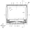
図1は、第1実施形態に係る電気光学装置100の平面図である。図2は、図1中のA−A線断面図である。なお、以下では、説明の便宜上、互いに直交するX軸、Y軸およびZ軸を適宜用いて説明する。また、X軸に沿う一方向をX1方向といい、X1方向とは反対の方向をX2方向という。同様に、Y軸に沿う一方向をY1方向といい、Y1方向とは反対の方向をY2方向という。Z軸に沿う一方向をZ1方向といい、Z1方向とは反対の方向をZ2方向という。
1A. First Embodiment 1A-1. Basic configuration FIG. 1 is a plan view of the electro-
図1および図2に示す電気光学装置100は、透過型の液晶表示装置である。図2に示すように、電気光学装置100は、透光性を有する素子基板2と、透光性を有する対向基板4と、枠状のシール部材8と、液晶層9とを有する。素子基板2は「第1基板」の例示である。対向基板4は「第2基板」の例示である。液晶層9は「電気光学層」の例示である。シール部材8は、素子基板2と対向基板4との間に配置される。液晶層9は、素子基板2、対向基板4およびシール部材8によって囲まれる領域内に配置される。素子基板2、液晶層9および対向基板4は、Z軸に沿って並ぶ。対向基板4が有する後述の第2基体41の表面がX−Y平面に平行である。以下では、素子基板2の厚さ方向であるZ1方向またはZ2方向からみることを「平面視」と言う。
The electro-
本実施形態の電気光学装置100では、光は、例えば対向基板4に入射し、液晶層9を透過して素子基板2から出射される。なお、光は、素子基板2に入射し、液晶層9を透過して対向基板4から出射されてもよい。当該光は可視光である。「透光性」とは、可視光に対する透過性を意味し、好ましくは可視光の透過率が50%以上であることをいう。また、図1に示す電気光学装置100は平面視で四角形状をなすが、電気光学装置100の平面視での形状は、これに限定されず、例えば円形等であってもよい。
In the electro-
図2に示すように、素子基板2は、第1基体21と配線層20と複数の画素電極28と第1配向膜29とを有する。第1基体21は、透光性および絶縁性を有する平板で構成される。第1基体21と複数の画素電極28との間には配線層20が配置される。画素電極28は、透光性を有しており、例えばITO(Indium Tin Oxide)またはIZO(Indium Zinc Oxide)等の透明導電材料で構成される。第1配向膜29は、素子基板2において最も液晶層9側に位置しており、液晶層9の液晶分子を配向させる。第1配向膜29の構成材料としては、例えばポリイミドおよび酸化ケイ素等が挙げられる。なお、配線層20の構成については、後で説明する。
As shown in FIG. 2, the
図2に示すように、対向基板4は、第2基体41と絶縁膜42と共通電極45と第2配
向膜46とを有する。共通電極45は「対向電極」の例示である。液晶層9は「電気光学
層」の例示である。第2基体41、絶縁膜42、共通電極45および第2配向膜46は、
この順に並ぶ。第2配向膜46が最も液晶層9側に位置する。第2基体41は、透光性お
よび絶縁性を有する平板で構成される。第2基体41は、例えば、ガラスまたは石英等で
構成される。絶縁膜42は、例えば酸化ケイ素等の透光性および絶縁性を有するケイ素系
の無機材料で形成される。共通電極45は、例えばITOまたはIZO等の透明導電材料
で構成される。第2配向膜46は、液晶層9の液晶分子を配向させる。第2配向膜46の
構成材料としては、例えばポリイミドおよび酸化ケイ素等が挙げられる。
As shown in FIG. 2, the facing
Arrange in this order. The
シール部材8は、例えばエポキシ樹脂等の各種硬化性樹脂を含む接着剤等を用いて形成される。シール部材8は、素子基板2および対向基板4のそれぞれに対して固着される。シール部材8の周方向での一部には、液晶分子を含む液晶材をシール部材8の内側に注入するための注入口81が形成される。注入口81は、各種樹脂材料を用いて形成される封止材80により封止される。
The sealing
液晶層9は、正または負の誘電異方性を有する液晶分子を含む。液晶層9は、液晶分子が第1配向膜29および第2配向膜46の双方に接するように素子基板2および対向基板4によって挟持される。液晶層9は、複数の画素電極28と共通電極45との間に配置され、電界による光学的特性が変化する。具体的には、液晶層9が有する液晶分子の配向は、液晶層9に印加される電圧に応じて変化する。つまり、液晶層9は、印加される電圧に応じて光を変調させることで階調表示を可能とする。
The
図1に示すように、素子基板2における対向基板4側の面には、複数の走査線駆動回路11とデータ線駆動回路12と、複数の外部端子14とが配置される。外部端子14には、走査線駆動回路11およびデータ線駆動回路12のそれぞれから引き回される引回配線15が接続される。
As shown in FIG. 1, a plurality of scanning
以上の構成の電気光学装置100は、画像を表示する表示領域A10と、表示領域A10を平面視で囲む周辺領域A20とを有する。表示領域A10には、行列状に配列される複数の画素Pが設けられる。1つの画素Pに対して1つの画素電極28が配置される。周辺領域A20には、走査線駆動回路11およびデータ線駆動回路12等が配置される。
The electro-
1A−2.電気的な構成
図3は、素子基板2の電気的な構成を示す等価回路図である。図3に示すように、素子基板2には、n本の走査線244とm本のデータ線246とn本の容量線としての第1定電位線245と、が設けられる。nおよびmはそれぞれ2以上の整数である。
1A-2. Electrical configuration FIG. 3 is an equivalent circuit diagram showing the electrical configuration of the
n本の走査線244は、それぞれY軸に沿って延在し、X軸に沿って等間隔で並ぶ。走査線244は、トランジスター23のゲートに電気的に接続される。また、n本の走査線244は、図1に示す走査線駆動回路11に電気的に接続される。n本の走査線244には、走査線駆動回路11から走査信号G1、G2、…、およびGnが線順次で供給される。
Each of the
図3に示すm本のデータ線246は、それぞれX軸に沿って延在し、Y軸に沿って等間隔で並ぶ。データ線246は、トランジスター23のソースに電気的に接続される。また、m本のデータ線246は、図1に示すデータ線駆動回路12に電気的に接続される。m本のデータ線246には、図1に示すデータ線駆動回路12から画像信号S1、S2、…、およびSmが並行に供給される。
The m
図3に示すn本の走査線244とm本のデータ線246とは、互いに絶縁され、平面視で格子状をなす。隣り合う2つの走査線244と隣り合う2つのデータ線246とで囲まれる領域が画素Pに対応する。1つの画素Pには、1つの画素電極28が設けられる。1つの画素電極28には、1つのトランジスター23が電気的に接続される。トランジスター23は、例えばスイッチング素子として機能するTFTである。
The
n本の第1定電位線245は、それぞれY軸に沿って延在し、X軸に沿って等間隔で並
ぶ。また、n本の第1定電位線245は、複数のデータ線246および複数の走査線24
4と絶縁され、これらに対して離間して形成される。第1定電位線245には、例えばグ
ランド電位等の固定電位が印加される。また、第1定電位線245と画素電極28との間
には、液晶容量に保持される電荷のリークを防止するために蓄積容量200が液晶容量と
並列に配置される。蓄積容量200は、供給された画像信号Smに応じて画素電極28の
電位を保持するための容量素子である。蓄積容量200は「容量」の例示である。
The n first constant
It is insulated from 4 and formed apart from these. A fixed potential such as a ground potential is applied to the first constant
走査信号G1、G2、…、およびGnが順次アクティブとなり、n本の走査線244が順次選択されると、選択される走査線244に接続されるトランジスター23がオン状態となる。すると、m本のデータ線246を介して表示すべき階調に応じた大きさの画像信号S1、S2、…、およびSmが、選択される走査線244に対応する画素Pに取り込まれ、画素電極28に印加される。これにより、画素電極28と図2に示す対向基板4が有する共通電極45との間に形成される液晶容量に、表示すべき階調に応じた電圧が印加され、印加される電圧に応じて液晶分子の配向が変化する。また、蓄積容量200によって、印加される電圧が保持される。このような液晶分子の配向の変化によって光が変調され、階調表示が可能となる。
When the scanning signals G1, G2, ..., And Gn are sequentially activated and
1A−3.素子基板2の構成
図4は、素子基板2の一部を示す断面図である。以下の説明では、Z1方向を上方とし、Z2方向を下方として説明する。図4に示すように、素子基板2の第1基体21には、遮光体241が設けられる。遮光体241は、トランジスター23ごとに設けられる。遮光体241は、遮光性および導電性を有する。遮光性とは、可視光に対する遮光性を意味し、具体的には可視光の透過率が10%以下であることをいう。なお、遮光体241は、第1基体21に設けられる凹部内に配置される。遮光体241の構成材料としては、例えば、タングステン(W)、チタン(Ti)、クロム(Cr)、鉄(Fe)およびアルミニウム(Al)等の金属、金属窒化物ならびに金属シリサイド等が挙げられる。これらの中でも、タングステンを用いることが好ましい。タングステンは耐熱性に優れるため、タングステンを用いることで、遮光体241によってトランジスター23への光の入射を特に効果的に防ぐことができる。
1A-3. Configuration of
遮光体241上には、配線層20が配置される。配線層20は、トランジスター23、走査線244、第1定電位線245、蓄積容量200、データ線246、および第2定電位線248を有する。また、配線層20は、絶縁性および透光性を有する絶縁体22を有する。絶縁体22は、層間絶縁膜221、222、223、224、225、226、227、228および229を有する。層間絶縁膜221、222、223、224、225、226、227、228および229は、この順に第1基体21から画素電極28に向かって配置される。層間絶縁膜221〜229は、それぞれ、例えば熱酸化またはCVD(chemical vapor deposition)法等で成膜される酸化ケイ素膜で構成される。配線層20が有する配線および電極は、絶縁体22を構成する膜同士の間に当該膜に接触した状態で配置される。
The
第1基体21上には、遮光体241を覆って層間絶縁膜221が配置される。層間絶縁膜221上にはトランジスター23が配置される。トランジスター23は、半導体層231、ゲート電極232およびゲート絶縁膜233を有する。半導体層231は、層間絶縁膜222と層間絶縁膜223との間に配置される。半導体層231は、ソース領域231a、ドレイン領域231b、チャネル領域231c、第1LDD(Lightly Doped Drain)領域231d、および第2LDD領域231eを有する。半導体層231は、例えば、ポリシリコンを成膜して形成され、チャネル領域231cを除く領域には、導電性を高める不純物がドープされる。第1LDD領域231dおよび第2LDD領域231e中の不純物濃度は、ソース領域231aおよびドレイン領域231b中の不純物濃度よりも低い。なお、第1LDD領域231dおよび第2LDD領域231eのうちの少なくとも一方は、省略してもよい。
An interlayer insulating
ゲート電極232は、層間絶縁膜222と層間絶縁膜223との間に配置される。ゲート電極232は、Z1方向からみて半導体層231のチャネル領域231cに重なる。ゲート電極232は、例えば、ポリシリコンに導電性を高める不純物がドープされることにより形成される。なお、ゲート電極232は、金属、金属シリサイドおよび金属化合物の導電性を有する材料を用いて形成されてもよい。また、ゲート電極232とチャネル領域231cとの間には、ゲート絶縁膜233が介在する。ゲート絶縁膜233は、例えば、熱酸化またはCVD法等で成膜される酸化ケイ素で構成される。
The
層間絶縁膜223と層間絶縁膜224との間には、走査線244が配置される。走査線244は、層間絶縁膜223を貫通するコンタクト部271を介してゲート電極232に接続される。なお、本実施形態では、ゲート電極232と遮光体241とは絶縁されているが、これらは電気的に接続されてもよい。この場合、遮光体241をバックゲートとして用いることができる。
A
層間絶縁膜224と層間絶縁膜225との間には、第1定電位線245が配置される。第1定電位線245にはシールド部270が接続される。シールド部270は、層間絶縁膜224を貫通して層間絶縁膜223の厚さ方向の途中位置までの間に配置される。また、シールド部270は、Z1方向からみて第2LDD領域231eと重なる。シールド部270は、走査線244からの漏れ電界がトランジスター23に影響することを抑制するシールドとして機能する。また、シールド部270は、半導体層231の遮光部として機能する。シールド部270には、第1定電位線245から固定電位が供給される。
A first constant
層間絶縁膜225上には、蓄積容量200が配置される。蓄積容量200は、第1容量25および第2容量26を有する。第1容量25は、層間絶縁膜225と層間絶縁膜226との間に配置される。第1容量25は、下部容量電極251、上部容量電極252、およびこれらの間に配置される誘電体層253を有する。下部容量電極251は、層間絶縁膜225を貫通するコンタクト部272を介して第1定電位線245に接続される。また、第2容量26は、層間絶縁膜226と層間絶縁膜227との間に配置される。第2容量26は、下部容量電極261、上部容量電極262、およびこれらの間に配置される誘電体層263を有する。下部容量電極261は、層間絶縁膜226を貫通するコンタクト部273を介して第1容量25の上部容量電極252に接続される。また、下部容量電極261は、層間絶縁膜222〜226を貫通するコンタクト部274を介してトランジスター23のドレイン領域231bに電気的に接続される。第1容量25の上部容量電極252は、図示しないコンタクト部等を介して、配線層20上に配置される画素電極28に電気的に接続される。
A storage capacity of 200 is arranged on the
層間絶縁膜227と層間絶縁膜228との間には、データ線246が配置される。データ線246は層間絶縁膜227および層間絶縁膜228に接触する。データ線246は、層間絶縁膜222〜227を貫通するコンタクト部275を介してトランジスター23のソース領域231aに電気的に接続される。また、層間絶縁膜228と層間絶縁膜229との間には、第2定電位線248が配置される。第2定電位線248は、図示しないコンタクト部等を介して第2容量26の上部容量電極262に電気的に接続される。第2定電位線248には、第1定電位線245と同様に、例えばグランド電位等の固定電位が印加される。第1定電位線245に供給される固定電位と第2定電位線248に供給される固定電位とは、同電位である。
A
下部容量電極251、上部容量電極252、下部容量電極261、および上部容量電極262は、例えば窒化チタン膜で構成される。走査線244、第1定電位線245、データ線246および第2定電位線248等の配線は、例えば、アルミニウム膜と窒化チタン膜との積層体で構成される。アルミニウム膜を含むことで、窒化チタン膜のみで構成される場合に比べて低抵抗化を図ることができる。なお、これら電極または配線のそれぞれは、前述の材料以外の材料で構成されてもよい。例えば、これら電極または配線のそれぞれは、タングステン(W)、チタン(Ti)、クロム(Cr)、鉄およびアルミニウム(Al)等の金属、金属窒化物、ならびに金属シリサイド等で構成されてもよい。
The
図5は、素子基板2の一部を示す平面図である。図5に示すように、素子基板2は、光が透過する複数の透光領域A11と、光を遮断する配線領域A12とを有する。複数の透光領域A11は、行列状に配置され、それぞれZ1方向からみてほぼ四角形状をなす。各透光領域A11には、画素電極28が設けられる。配線領域A12は、Z1方向からみて格子状をなし、透光領域A11を囲む。配線領域A12には、トランジスター23、蓄積容量200、走査線244、データ線246、第1定電位線245および複数の第2定電位線248が設けられる。複数の走査線244と複数のデータ線246とは、Z1方向からみて格子状をなす。複数の第1定電位線245と複数の第2定電位線248とは、Z1方向からみて格子状をなす。トランジスター23および蓄積容量200は、走査線244とデータ線246との交差位置に配置される。
FIG. 5 is a plan view showing a part of the
また、図4に示すコンタクト部271〜275およびシールド部270は、配線領域A12に設けられる。別の言い方をすれば、コンタクト部271〜275およびシールド部270は、Z1方向からみて、隣り合う2個の画素電極28の間に配置される。なお、当該隣り合う2個の画素電極28とは、X軸、Y軸、またはX−Y平面においてX軸およびY軸の両方と交差する軸に沿って隣り合う任意の2個の画素電極28のことをいう。複数の画素電極28のうちの任意の1個の画素電極28を「第1画素電極」とし、それと隣り合う1個の画素電極28を「第2画素電極」とすると、「第1画素電極」と「第2画素電極」との間にコンタクト部271〜275およびシールド部270は設けられる。
Further, the contact portions 271-275 and the
1A−4.コンタクト部
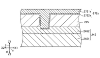
図6は、下部容量電極251に接続されるコンタクト部272を示す断面図である。なお、コンタクト部272〜274は、同様の構成であるため、以下ではコンタクト部272について代表して説明する。また、以下の説明では、コンタクト部272が「導電部」に相当し、層間絶縁膜225が「絶縁層」に相当し、第1定電位線245が「第2導電膜」に相当し、第1容量25の下部容量電極251が「導電膜」に相当する。よって、下部容量電極251は「第1導電膜」に相当する。下部容量電極251は、層間絶縁膜225と前述の液晶層9との間に位置する。
1A-4. Contact section FIG. 6 is a cross-sectional view showing a
図6に示すように、コンタクト部272は、層間絶縁膜225に設けられる。具体的には、コンタクト部272は、層間絶縁膜225に形成された貫通孔であるコンタクトホールを埋めるよう設けられる。コンタクト部272の一端は第1定電位線245に接続され、他端は下部容量電極251に接続される。図6に示す例では、第1定電位線245は、アルミニウム膜2451と、窒化チタン膜2452との積層体で構成される。窒化チタン膜2452は、コンタクト部272に接触する。なお、コンタクト部272は、窒化チタン膜2452を貫通し、アルミニウム膜2451に接触してもよい。
As shown in FIG. 6, the
コンタクト部272は、第2層2722と第1層2721との積層体で構成される。第1層2721は、タングステンを含む。タングステンは耐熱性に優れ、アスペクト比が高いコンタクトホールに対して埋め込み易い材料である。そのため、第1層2721がタングステンを含むことで、コンタクト部272における欠陥の発生を抑制することができる。また、第2層2722は、第1層2721と異なる材料で構成され、第1層2721と層間絶縁膜225との間に位置する。第2層2722が第1層2721と異なる材料であることで、第1層2721のみで構成される場合に比べ、第2層2722の材料等に応じた機能がコンタクト部271に付与される。例えば、第2層2722は、層間絶縁膜225に対する第1層2721の密着性を向上させるために設けられる。例えば、第2層2722は、タングステンナイトライド(WN)、チタンナイトライド(TiN)およびタングステンシリサイド(WSi)等を含む。特にタングステンナイトライドであることで、第1層2721と層間絶縁膜225との密着性を高めることができる。
The
コンタクト部272は、下部容量電極251を構成する材料とは異なる材料で構成されており、Z1方向からみて下部容量電極251と重なっている。すなわち、コンタクト部272の材料とは異なる材料の下部容量電極251によってコンタクト部272は覆われる。かかるコンタクト部272が設けられることで、従来のようにコンタクトホールの壁面に沿って下部容量電極251を設けなくて済む。そのため、下部容量電極251の微細化を図ることができるとともに、下部容量電極251を充分な厚さで形成できるので耐電圧の低下を抑制することができる。
The
図6に示すように、コンタクト部272における下部容量電極251と接触する面272aは、層間絶縁膜225における下部容量電極251と接触する面225aと、Z1方向における位置が異なる。面225aは、特に、層間絶縁膜225における層間絶縁膜226と接触する部分である。本実施形態では、コンタクト部272の面272aは、層間絶縁膜225の面225aに対してZ1方向に位置する。別の言い方をすれば、コンタクト部272は、層間絶縁膜225からZ1方向に突出する部分を有する。それゆえ、層間絶縁膜225上およびコンタクト部272上に設けられた下部容量電極251の面251aは、層間絶縁膜225の面225aとコンタクト部272の面272aとのZ1方向における位置の違いに応じた凹凸を有する。そのため、面251aが平坦面である場合に比べて面251aの面積を増やすことができる。なお、面251aは、下部容量電極251における層間絶縁膜225と反対の面であり、誘電体層253に接触する面である。同様に、上部容量電極252の面252aも凹凸を有する。そのため、面252aの面積を増やすことができる。なお、面252aは、上部容量電極252における誘電体層253と接触する面である。このように、面251aおよび面252aの各面積が増えることで、第1容量25の保持容量を増加させることができる。それゆえ、コンタクト部272を設けることで、第1容量25の保持容量の低下を抑制しつつ、第1容量25の微細化を図ることができる。よって、第1容量25がコンタクトホールの壁面に沿って形成されなくても保持容量の増加を図ることができる。
As shown in FIG. 6, the
また、コンタクト部272は、Z1方向からみて第1定電位線245と重なり、第1定電位線245に接続される。つまり、第1定電位線245と下部容量電極251との接続には、コンタクト部272が用いられる。コンタクト部272はコンタクトホールを埋めるよう形成されているため、コンタクトホールの幅を従来よりも小さくしても耐電圧の低下が抑制される。そのため、コンタクト部272によって、第1定電位線245と下部容量電極251とが接続されることで、第1定電位線245と下部容量電極251との間の接続不良等が抑制される。
Further, the
また、前述のように、コンタクト部272は、Z1方向からみて、図4に示す隣り合う2個の画素電極28の間に配置される。つまり、コンタクト部272は、Z1方向からみて画素電極28と重ならない。前述のように、コンタクト部272は、層間絶縁膜225のコンタクトホールを埋めるように設けられる。そのため、配線領域A12の面積の増加を抑制し、素子基板2の開口率の低下を防ぎつつ、素子基板2の高精細化を図ることができる。
Further, as described above, the
図7、図8および図9は、コンタクト部272の製造方法について説明するための断面図である。コンタクト部272は、ダマシン法等を用いて形成される。具体的にはまず、層間絶縁膜225にコンタクトホールが形成され、当該コンタクトホールにタングステン等が埋め込まれることにより図7に示す導電材料層272xが形成される。導電材料層272xは、例えばタングステンを含む第1材料層2721xと、第1材料層2721xとは異なる材料で構成される第2材料層2722xとの積層体である。
7, 8 and 9 are cross-sectional views for explaining a method of manufacturing the
次に、図8に示すように、導電材料層272xに対してCMP(chemical mechanical polishing)等の研磨による平坦化処理が施されることにより、コンタクト部272が形成される。本実施形態では、例えば、第1材料層2721xおよび第2材料層2722xの各材料等に応じて研磨液等が選定され、第1材料層2721xおよび第2材料層2722xの各表面のZ1方向における位置がほぼ同一になるよう平坦化処理が行われる。
Next, as shown in FIG. 8, the
次に、図9に示すように、ウエットエッチング等により、層間絶縁膜225の一部が除去される。これにより、コンタクト部272は、層間絶縁膜225よりもZ1方向に突出する。当該ウエットエッチングでは、コンタクト部272が除去され難く、層間絶縁膜223が除去され易いエッチング液が用いられる。例えばBHF(バッファードフッ酸)、またはDHF(希フッ酸)等のフッ素系のエッチング液が用いられる。かかる方法によれば、プロセスを過度に増やすことなく、層間絶縁膜225よりもZ1方向に突出する部分を有するコンタクト部272を形成することができる。
Next, as shown in FIG. 9, a part of the
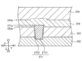
図10は、走査線244に接続されるコンタクト部271を示す断面図である。なお、コンタクト部271および275は同様の構成であるため、以下ではコンタクト部271について代表して説明する。また、コンタクト部271について、前述のコンタクト部272と同様の事項は適宜説明を省略する。以下の説明では、コンタクト部271が「導電部」に相当し、層間絶縁膜223が「絶縁層」に相当し、ゲート電極232が「第2導電膜」に相当し、走査線244が「導電膜」に相当する。よって、走査線244は「第1導電膜」に相当する。走査線244は、層間絶縁膜223と前述の液晶層9との間に位置する。
FIG. 10 is a cross-sectional view showing a
図10に示すように、コンタクト部271は、層間絶縁膜223に設けられる。具体的には、コンタクト部271は、層間絶縁膜223に形成されたコンタクトホールを埋めるよう設けられる。コンタクト部271の一端は走査線244に接続され、他端はゲート電極232に接続される。コンタクト部271は、コンタクト部272と同様に、例えば、タングステンを含む第1層2711と、第1層2711とは異なる材料で構成される第2層2712とを含む。
As shown in FIG. 10, the
コンタクト部271は、走査線244を構成する材料とは異なる材料で構成され、Z1方向からみて走査線244と重なる。かかるコンタクト部271が設けられることで、走査線244は、従来のようにコンタクトホールの壁面に沿った部分を有さずに済む。そのため、走査線244の微細化を図ることができるとともに、走査線244を充分な厚さで形成できるので耐電圧の低下を抑制することができる。
The
図10に示すように、コンタクト部271における走査線244と接触する面271aは、層間絶縁膜223における走査線244と接触する面223aとZ1方向における位置が異なる。面223aは、特に、層間絶縁膜223における層間絶縁膜224と接触する部分である。本実施形態では、コンタクト部271の面271aは、層間絶縁膜223の面223aに対してZ1方向に位置する。別の言い方をすれば、コンタクト部271は、層間絶縁膜223からZ1方向に突出する部分を有する。それゆえ、コンタクト部271の面271aが層間絶縁膜223の面223aとで同一平面上に位置する場合に比べて、走査線244に対するコンタクト部271の接触面積を増やすことができる。そのため、走査線244とコンタクト部271との間での抵抗を低減することができる。よって、走査線244の耐電圧の低下および抵抗増加を抑制しつつ、走査線244の微細化を図ることができる。また、走査線244の面244aは、層間絶縁膜223の面223aとコンタクト部271の面271aとのZ1方向における位置の違いに応じた凹凸を有する。コンタクト部271が層間絶縁膜223の面223aに対して突出している分、走査線244の断面積が増加していると捉えることができる。よって、走査線244の低抵抗化を図ることができる。
As shown in FIG. 10, the
図4に示すシールド部270も、前述のコンタクト部272と同様である。以下、シールド部270について説明するが、前述のコンタクト部272と同様の事項は適宜説明を省略する。シールド部270が「導電部」である場合、層間絶縁膜223および224が「絶縁層」に相当し、第1定電位線245が「導電膜」に相当する。第1定電位線245は、層間絶縁膜224と前述の液晶層9との間に位置する。
The
図4に示すシールド部270は、層間絶縁膜223および224に形成された凹部を埋めるよう設けられ、Z1方向からみて第1定電位線245と重なっている。かかる構成のシールド部270であれば、第1定電位線245に接続されたシールド部270を設けても第1定電位線245の微細化を図ることができる。
The
また、図示はしないが、画素電極28に接続されたコンタクト部も、コンタクト部271と同様の構成であってもよい。
Further, although not shown, the contact portion connected to the
1B.第2実施形態
第2実施形態を説明する。なお、以下の各例示において機能が第1実施形態と同様である要素については、第1実施形態の説明で使用した符号を流用して各々の詳細な説明を適宜に省略する。
1B. Second Embodiment The second embodiment will be described. For the elements having the same functions as those of the first embodiment in each of the following examples, the reference numerals used in the description of the first embodiment will be diverted and detailed description of each will be omitted as appropriate.
図11は、第2実施形態における下部容量電極251に接続されるコンタクト部272Aを示す断面図である。コンタクト部272Aの面272aは、層間絶縁膜225の面225aに対してZ2方向に位置する。別の言い方をすれば、コンタクト部272Aは、層間絶縁膜225の面225aに対してZ2方向に凹む部分を有する。それゆえ、本実施形態においても第1実施形態と同様に、下部容量電極251の面251aは、面272aと面225aとのZ1方向における位置の違いに応じた凹凸を有する。面251aが凹凸を有することで、面251aが平坦面である場合に比べて、面251aの面積を増やすことができる。また、上部容量電極252の面252aも凹凸を有するため、面252aの面積を増やすことができる。よって、本実施形態においても第1実施形態と同様に、第1容量25の保持容量を増やすことができる。それゆえ、第1容量25の保持容量の低下を抑制しつつ、第1容量25の微細化を図ることができる。
FIG. 11 is a cross-sectional view showing a
図11に示すコンタクト部272Aは、第1実施形態におけるコンタクト部272と同様の方法で形成される。ただし、例えば研磨液またはエッチング液が第1実施形態とは異なる。例えば、第1実施形態で用いた研磨液に含まれる粒子よりも大きい粒子を用い、層間絶縁膜225よりもコンタクト部272Aが研磨され易い条件で平坦化処理が行われる。なお、本実施形態では、第1実施形態におけるウエットエッチングの処理は適宜省略してもよい。
The
図12は、走査線244に接続されるコンタクト部271Aを示す断面図である。コンタクト部271Aの面271aは、層間絶縁膜223の面223aに対してZ2方向に位置する。別の言い方をすれば、コンタクト部271Aは、層間絶縁膜223の面223aに対してZ2方向に凹む部分を有する。また、本実施形態では、走査線244の面244aは平坦面である。走査線244の面244aが平坦面となるよう、走査線244は充分な厚さを有する。そのため、コンタクト部271Aが面223aに対して凹んでいる分、走査線244の断面積を増やすことができる。よって、走査線244の抵抗増加を抑制しつつ、走査線244の微細化を図ることができる。
FIG. 12 is a cross-sectional view showing a
なお、図示はしないが、第2実施形態におけるコンタクト部273〜275およびシールド部270のZ1方向における各位置は、本実施形態におけるコンタクト部272のZ1方向における各位置と同様である。第2実施形態におけるコンタクト部271〜275およびシールド部270によっても、第1実施形態と同様に耐電圧等の特性を低減しつつ配線等の微細化を図ることができる。
Although not shown, the positions of the
1C.第3実施形態
第3実施形態を説明する。なお、以下の各例示において機能が第1実施形態と同様である要素については、第1実施形態の説明で使用した符号を流用して各々の詳細な説明を適宜に省略する。
1C. Third Embodiment The third embodiment will be described. For the elements having the same functions as those of the first embodiment in each of the following examples, the reference numerals used in the description of the first embodiment will be diverted and detailed description of each will be omitted as appropriate.
図13は、第3実施形態における下部容量電極251に接続されるコンタクト部272Bを示す断面図である。図13に示すコンタクト部272Bが有する第1層2721における下部容量電極251と接触する面2721aの位置と、第2層2722における下部容量電極251と接触する面2722aの位置とは、Z1方向において異なる。また、面2721aおよび面2722aのそれぞれは、層間絶縁膜225の面225aとZ1方向における位置が異なる。本実施形態では、面2722aのうちの最もZ1方向に位置する部分は、面2721aのうちの最もZ1方向に位置する部分と、面225aとの間に位置する。かかるコンタクト部272Bによっても、下部容量電極251の面251aに凹凸を形成することができる。同様に、上部容量電極252の面252aに凹凸を形成することができる。そのため、第1容量25の保持容量を増加させつつ、第1容量25の微細化を図ることができる。
FIG. 13 is a cross-sectional view showing a
図13に示すコンタクト部272Bは、第1実施形態におけるコンタクト部272と同様の方法で形成される。ただし、例えば研磨液またはエッチング液が第1実施形態とは異なる。例えば、第2層2722よりも第1層2711が研磨され易い研磨液を用いて平坦化処理が行われる。
The
なお、図示はしないが、第3実施形態におけるコンタクト部271、273〜275およびシールド部270のZ1方向における各位置は、本実施形態におけるコンタクト部272のZ1方向における各位置と同様である。第3実施形態におけるコンタクト部271〜275およびシールド部270によっても、第1実施形態と同様に耐電圧等の特性を低減しつつ配線等の微細化を図ることができる。
Although not shown, the positions of the
1D.変形例
以上に例示した各形態は多様に変形され得る。前述の各形態に適用され得る具体的な変形の態様を以下に例示する。以下の例示から任意に選択された2以上の態様は、相互に矛盾しない範囲で適宜に併合され得る。
1D. Modification Examples Each of the above-exemplified forms can be variously transformed. Specific modifications that can be applied to each of the above-described forms are illustrated below. Two or more embodiments arbitrarily selected from the following examples can be appropriately merged to the extent that they do not contradict each other.
図14は、変形例におけるコンタクト部272Bの断面図である。第3実施形態では、下部容量電極251の面251aは、第1層2711の面2721aと第2層2722の面2722aとのZ1方向における位置の違いに応じた凹凸を有する。しかし、面251aは、面2721aと面2722aとに応じた凹凸を有さなくてもよい。
FIG. 14 is a cross-sectional view of the
図15は、変形例におけるコンタクト部272Cの断面図である。図14に示すように、Z1方向において、面2721aと面225aとの間に面2722aが位置してもよい。特に、面2722aのうちの最もZ1方向に位置する部分は、面2721aのうちの最もZ1方向に位置する部分と、面225aとの間に位置してもよい。
FIG. 15 is a cross-sectional view of the
第3実施形態では、面2721aおよび面2722aは、面225aに対してZ1方向に位置する。しかし、面2721aおよび面2722aは、面225aに対してZ2方向に位置してもよい。また、面2721aおよび面2722aのいずれか一方が、面225aに対してZ1方向に位置し、他方が、面225aに対してZ2方向に位置してもよい。また、面2721aおよび面2722aのいずれか一方が、面225aと同一平面に位置し、他方が、面225aに対してZ1方向またはZ2方向に位置してもよい。すなわち、コンタクト部272の面272aは、層間絶縁膜225の面225aとZ1方向において異なる部分を有すればよい。特に、面272aは、面225aのうち層間絶縁膜226と接触する部分とZ1方向において異なる部分を有すればよい。なお、コンタクト部272以外のコンタクト部についても同様である。また、配線層20が有する複数のコンタクト部のうちの少なくとも1つが、前述のように、対応する層間絶縁膜の上面よりも突出していたり、凹んでいたりすればよい。全てのコンタクト部が、前述のような層間絶縁膜との位置関係を満足しなくてもよい。
In the third embodiment, the
第1実施形態では、コンタクト部272は、第1層2721および第2層2722で構成されるが、コンタクト部272は、第1層2721および第2層2722以外で構成されてもよい。例えば、コンタクト部272は、単層であってもよいし、3層以上で構成されてもよい。例えば、コンタクト部272は、第1層2721のみで構成されてもよい。また、コンタクト部272の材料としては、タングステンに限定されない。例えば、コンタクト部272の材料は、アルミニウムおよび銅(Cu)等のタングステン以外の金属を含んでもよい。なお、他のコンタクト部271、273、274および275、ならびにシールド部270等も同様に、タングステン以外の材料で構成されてもよい。
In the first embodiment, the
第1実施形態では、1個の第1容量25に接続されるコンタクト部272の数は1個であるが、2個以上であってもよい。他のコンタクト部271、273、274および275、ならびにシールド部270の各数も2個以上であってもよい。
In the first embodiment, the number of
前述の実施形態では、素子基板2が「導電部」を有する構成を例に説明したが、対向基板4が「導電部」を有してもよい。素子基板2および対向基板4の一方または双方が「導電部」を有すればよい。
In the above-described embodiment, the configuration in which the
前述の実施形態では、蓄積容量200は、第1容量25および第2容量26を有するが、第1容量25および第2容量26の一方は省略されてもよい。また、走査線244、第1定電位線245、データ線246、および第2定電位線248等の配線層20が有する配線の積層順は、図4に示す例に限定されず任意である。また、第1定電位線245および第2定電位線248は、それぞれ容量線として機能するが、これら双方またはいずれか一方は、容量線として機能しなくてもよい。
In the above-described embodiment, the
前述の実施形態では、トランジスターとしてTFTを用いる場合を例に説明したが、トランジスターはTFTに限定されず、例えば、MOSFET(metal-oxide-semiconductor field-effect transistor)等であってもよい。 In the above-described embodiment, the case where a TFT is used as the transistor has been described as an example, but the transistor is not limited to the TFT, and may be, for example, a MOSFET (metal-oxide-semiconductor field-effect transistor) or the like.
前述の実施形態では、アクティブマトリクス駆動方式の電気光学装置100が例示されるが、これに限定されず、電気光学装置の駆動方式は、例えば、パッシブマトリクス駆動方式等でもよい。
In the above-described embodiment, the electro-
2.電子機器
電気光学装置100は、各種電子機器に用いることができる。
2. Electronic device The electro-
図16は、電子機器の一例であるパーソナルコンピューター2000を示す斜視図である。パーソナルコンピューター2000は、各種の画像を表示する電気光学装置100と、電源スイッチ2001およびキーボード2002が設置される本体部2010と、制御部2003と、を有する。制御部2003は、例えばプロセッサーおよびメモリーを含み、電気光学装置100の動作を制御する。
FIG. 16 is a perspective view showing a
図17は、電子機器の一例であるスマートフォン3000を示す斜視図である。スマートフォン3000は、操作ボタン3001と、各種の画像を表示する電気光学装置100と、制御部3002と、を有する。操作ボタン3001の操作に応じて電気光学装置100に表示される画面内容が変更される。制御部3002は、例えばプロセッサーおよびメモリーを含み、電気光学装置100の動作を制御する。
FIG. 17 is a perspective view showing a
図18は、電子機器の一例であるプロジェクターを示す模式図である。投射型表示装置4000は、例えば、3板式のプロジェクターである。電気光学装置1rは、赤色の表示色に対応する電気光学装置100であり、電気光学装置1gは、緑の表示色に対応する電気光学装置100であり、電気光学装置1bは、青色の表示色に対応する電気光学装置100である。すなわち、投射型表示装置4000は、赤、緑および青の表示色に各々対応する3個の電気光学装置1r、1g、1bを有する。制御部4005は、例えばプロセッサーおよびメモリーを含み、電気光学装置100の動作を制御する。
FIG. 18 is a schematic view showing a projector which is an example of an electronic device. The projection
照明光学系4001は、光源である照明装置4002からの出射光のうち赤色成分rを電気光学装置1rに供給し、緑色成分gを電気光学装置1gに供給し、青色成分bを電気光学装置1bに供給する。各電気光学装置1r、1g、1bは、照明光学系4001から供給される各単色光を表示画像に応じて変調するライトバルブ等の光変調器として機能する。投射光学系4003は、各電気光学装置1r、1g、1bからの出射光を合成して投射面4004に投射する。
The illumination
以上の電子機器は、前述の電気光学装置100と、制御部2003、3002または4005と、を備える。電気光学装置100は前述のように特性の低下を抑制しつつ高精細化を図ることができる。そのため、パーソナルコンピューター2000、スマートフォン3000または投射型表示装置4000の表示品質を高めることができる。
The above electronic device includes the above-mentioned electro-
なお、本発明の電気光学装置が適用される電子機器としては、例示した機器に限定されず、例えば、PDA(Personal Digital Assistants)、デジタルスチルカメラ、テレビ、ビデオカメラ、カーナビゲーション装置、車載用の表示器、電子手帳、電子ペーパー、電卓、ワードプロセッサー、ワークステーション、テレビ電話、およびPOS(Point of sale)端末等が挙げられる。さらに、本発明が適用される電子機器としては、プリンター、スキャナー、複写機、ビデオプレーヤー、またはタッチパネルを備えた機器等が挙げられる。 The electronic device to which the electro-optical device of the present invention is applied is not limited to the illustrated device, and is, for example, a PDA (Personal Digital Assistants), a digital still camera, a television, a video camera, a car navigation device, or an in-vehicle device. Examples include displays, electronic organizers, electronic papers, calculators, word processors, workstations, videophones, and POS (Point of sale) terminals. Further, examples of the electronic device to which the present invention is applied include a printer, a scanner, a copying machine, a video player, a device provided with a touch panel, and the like.
以上、好適な実施形態に基づいて本発明を説明したが、本発明は前述の各実施形態に限定されない。また、本発明の各部の構成は、前述の実施形態の同様の機能を発揮する任意の構成に置換でき、また、任意の構成を付加できる。 Although the present invention has been described above based on the preferred embodiments, the present invention is not limited to the above-described embodiments. Further, the configuration of each part of the present invention can be replaced with an arbitrary configuration that exhibits the same function as that of the above-described embodiment, and an arbitrary configuration can be added.
また、前述した説明では、本発明の電気光学装置の一例として液晶装置について説明したが、本発明の電気光学装置はこれに限定されない。例えば、本発明の電気光学装置は、イメージセンサー等にも適用することができる。また、例えば、有機EL(electro luminescence)、無機ELまたは発光ポリマー等の発光素子を用いた表示パネルに対しても前述の実施形態と同様に本発明が適用され得る。また、着色された液体と当該液体に分散された白色の粒子とを含むマイクロカプセルを用いた電気泳動表示パネルに対しても前述の実施形態と同様に本発明が適用され得る。 Further, in the above description, the liquid crystal device has been described as an example of the electro-optical device of the present invention, but the electro-optical device of the present invention is not limited to this. For example, the electro-optical device of the present invention can also be applied to an image sensor or the like. Further, for example, the present invention can be applied to a display panel using a light emitting element such as an organic EL (electroluminescence), an inorganic EL, or a light emitting polymer in the same manner as in the above-described embodiment. Further, the present invention can be applied to an electrophoresis display panel using microcapsules containing a colored liquid and white particles dispersed in the liquid in the same manner as in the above-described embodiment.
2…素子基板、4…対向基板、8…シール部材、9…液晶層、11…走査線駆動回路、12…データ線駆動回路、14…外部端子、15…引回配線、20…配線層、21…第1基体、22…絶縁体、23…トランジスター、25…第1容量、26…第2容量、28…画素電極、29…第1配向膜、41…第2基体、42…絶縁膜、45…共通電極、46…第2配向膜、80…封止材、81…注入口、100…電気光学装置、200…蓄積容量、221…層間絶縁膜、222…層間絶縁膜、223…層間絶縁膜、224…層間絶縁膜、225…層間絶縁膜、226…層間絶縁膜、227…層間絶縁膜、228…層間絶縁膜、229…層間絶縁膜、231…半導体層、231a…ソース領域、231b…ドレイン領域、231c…チャネル領域、231d…第1LDD領域、231e…第2LDD領域、232…ゲート電極、233…ゲート絶縁膜、241…遮光体、244…走査線、245…第1定電位線、246…データ線、248…第2定電位線、251…下部容量電極、252…上部容量電極、253…誘電体層、261…下部容量電極、262…上部容量電極、263…誘電体層、270…シールド部、271…コンタクト部、271A…コンタクト部、272…コンタクト部、272A…コンタクト部、272B…コンタクト部、272C…コンタクト部、273…コンタクト部、274…コンタクト部、275…コンタクト部、2000…パーソナルコンピューター、2001…電源スイッチ、2002…キーボード、2003…制御部、2010…本体部、2451…アルミニウム膜、2452…窒化チタン膜、2711…第1層、2712…第2層、2721…第1層、2722…第2層、272x…導電材料層、2721x…第1材料層、2722x…第2材料層、3000…スマートフォン、3001…操作ボタン、3002…制御部、4000…投射型表示装置、4001…照明光学系、4002…照明装置、4003…投射光学系、4004…投射面、4005…制御部、A10…表示領域、A20…周辺領域、A11…透光領域、A12…配線領域、P…画素、223a…面、225a…面、244a…面、251a…面、252a…面、271a…面、272a…面、2721a…面、2722a…面。 2 ... element substrate, 4 ... opposed substrate, 8 ... seal member, 9 ... liquid crystal layer, 11 ... scanning line drive circuit, 12 ... data line drive circuit, 14 ... external terminal, 15 ... routing wiring, 20 ... wiring layer, 21 ... 1st substrate, 22 ... Insulator, 23 ... Transistor, 25 ... 1st capacitance, 26 ... 2nd capacitance, 28 ... Pixel electrode, 29 ... 1st alignment film, 41 ... 2nd substrate, 42 ... Insulating film, 45 ... common electrode, 46 ... second alignment film, 80 ... encapsulant, 81 ... injection port, 100 ... electro-optical device, 200 ... storage capacity, 221 ... interlayer insulating film, 222 ... interlayer insulating film, 223 ... interlayer insulation Film, 224 ... interlayer insulating film, 225 ... interlayer insulating film, 226 ... interlayer insulating film, 227 ... interlayer insulating film, 228 ... interlayer insulating film, 229 ... interlayer insulating film, 231 ... semiconductor layer, 231a ... source region, 231b ... Drain region, 231c ... Channel region, 231d ... First LDD region, 231e ... Second LDD region, 232 ... Gate electrode, 233 ... Gate insulating film, 241 ... Shading body, 244 ... Scanning line, 245 ... First constant potential line, 246 ... data line, 248 ... second constant potential line, 251 ... lower capacitance electrode, 252 ... upper capacitance electrode, 253 ... dielectric layer, 261 ... lower capacitance electrode, 262 ... upper capacitance electrode, 263 ... dielectric layer, 270 ... Shield part, 271 ... Contact part, 271A ... Contact part, 272 ... Contact part, 272A ... Contact part, 272B ... Contact part, 272C ... Contact part, 273 ... Contact part, 274 ... Contact part, 275 ... Contact part, 2000 ... Personal computer, 2001 ... power switch, 2002 ... keyboard, 2003 ... control unit, 2010 ... main body unit, 2451 ... aluminum film, 2452 ... titanium nitride film, 2711 ... first layer, 2712 ... second layer, 2721 ... first layer , 2722 ... 2nd layer, 272x ... Conductive material layer, 2721x ... 1st material layer, 2722x ... 2nd material layer, 3000 ... Smartphone, 3001 ... Operation button, 3002 ... Control unit, 4000 ... Projection type display device, 4001 ... Illumination optical system, 4002 ... Illumination device, 4003 ... Projection optical system, 4004 ... Projection surface, 4005 ... Control unit, A10 ... Display area, A20 ... Peripheral area, A11 ... Translucent area, A12 ... Wiring area, P ... Pixels, 223a ... surface, 225a ... surface, 244a ... surface, 251a ... surface, 252a ... surface, 271a ... surface, 272a ... surface, 2721a ... surface, 2722a ... surface.
Claims (7)
前記基板に配置された画素電極と、
前記画素電極に対向する対向電極と、
前記画素電極と前記対向電極との間に配置された電気光学層と、
前記基板と前記画素電極との間に配置された絶縁層と、
前記絶縁層と前記電気光学層との間に配置され、前記絶縁層に接触する配線または電極である導電膜を含み、前記画素電極に電気的に接続された容量と、
前記絶縁層に設けられたコンタクトホール内に配置され、前記導電膜に接続される導電部と、を有し、
前記導電部は、前記導電膜を構成する材料とは異なる材料で構成され、かつ前記絶縁層の厚さ方向からみて前記導電膜と重なり、
前記導電部における前記導電膜と接触する領域は、前記絶縁層における前記導電膜と接触する領域と前記厚さ方向における位置が異なる部分を有し、
前記導電部は、タングステンを含む第1層と、前記第1層と前記絶縁層との間に配置され、前記第1層と異なる材料で構成される第2層とを含み、
前記第1層における前記導電膜と接触する領域の位置と、前記第2層における前記導電膜と接触する領域の位置とは、前記厚さ方向において異なることを特徴とする電気光学装置。 With the board
Pixel electrodes arranged on the substrate and
The counter electrode facing the pixel electrode and the counter electrode
An electro-optic layer arranged between the pixel electrode and the counter electrode,
An insulating layer arranged between the substrate and the pixel electrodes,
A capacitance that is disposed between the insulating layer and the electro-optical layer, includes a conductive wire or electrode that is in contact with the insulating layer, and is electrically connected to the pixel electrode.
It has a conductive portion that is arranged in a contact hole provided in the insulating layer and is connected to the conductive film.
The conductive portion is made of a material different from the material constituting the conductive film, and overlaps with the conductive film when viewed from the thickness direction of the insulating layer.
Regions in contact with the conductive film in the conductive portion, the conductive film and a position in the a region thickness direction in contact in the insulating layer have a different part,
The conductive portion includes a first layer containing tungsten and a second layer arranged between the first layer and the insulating layer and made of a material different from the first layer.
An electro-optical device characterized in that the position of a region in contact with the conductive film in the first layer and the position of a region in contact with the conductive film in the second layer are different in the thickness direction.
前記絶縁層における前記第1導電膜とは反対に設けられ、配線または電極である第2導電膜を備え、
前記導電部は、前記厚さ方向からみて前記第2導電膜と重なり、前記第2導電膜に接続される請求項1から4のいずれか1項に記載の電気光学装置。 The conductive film is the first conductive film and
A second conductive film provided in the insulating layer opposite to the first conductive film, which is a wiring or an electrode, is provided.
The electro-optical device according to any one of claims 1 to 4 , wherein the conductive portion overlaps with the second conductive film when viewed from the thickness direction and is connected to the second conductive film.
前記導電部は、前記厚さ方向からみて前記画素電極と前記第2画素電極との間に位置する請求項1から5のいずれか1項に記載の電気光学装置。 It has a second pixel electrode adjacent to the pixel electrode, and has
The electro-optical device according to any one of claims 1 to 5 , wherein the conductive portion is located between the pixel electrode and the second pixel electrode when viewed from the thickness direction.
前記電気光学装置の動作を制御する制御部と、を有することを特徴とする電子機器。 The electro-optical device according to any one of claims 1 to 6.
An electronic device including a control unit that controls the operation of the electro-optical device.
Priority Applications (2)
| Application Number | Priority Date | Filing Date | Title |
|---|---|---|---|
| JP2019153544A JP6939857B2 (en) | 2019-08-26 | 2019-08-26 | Electro-optics and electronic equipment |
| US16/999,076 US20210063830A1 (en) | 2019-08-26 | 2020-08-21 | Electro-optical device and electronic apparatus |
Applications Claiming Priority (1)
| Application Number | Priority Date | Filing Date | Title |
|---|---|---|---|
| JP2019153544A JP6939857B2 (en) | 2019-08-26 | 2019-08-26 | Electro-optics and electronic equipment |
Publications (3)
| Publication Number | Publication Date |
|---|---|
| JP2021033073A JP2021033073A (en) | 2021-03-01 |
| JP2021033073A5 JP2021033073A5 (en) | 2021-04-08 |
| JP6939857B2 true JP6939857B2 (en) | 2021-09-22 |
Family
ID=74678254
Family Applications (1)
| Application Number | Title | Priority Date | Filing Date |
|---|---|---|---|
| JP2019153544A Active JP6939857B2 (en) | 2019-08-26 | 2019-08-26 | Electro-optics and electronic equipment |
Country Status (2)
| Country | Link |
|---|---|
| US (1) | US20210063830A1 (en) |
| JP (1) | JP6939857B2 (en) |
Families Citing this family (2)
| Publication number | Priority date | Publication date | Assignee | Title |
|---|---|---|---|---|
| JP6813045B2 (en) * | 2019-03-14 | 2021-01-13 | セイコーエプソン株式会社 | Electro-optics and electronic equipment |
| CN110780497A (en) * | 2019-10-22 | 2020-02-11 | 深圳市华星光电技术有限公司 | Wiring structure of display panel, wiring method of display panel and display panel |
Family Cites Families (12)
| Publication number | Priority date | Publication date | Assignee | Title |
|---|---|---|---|---|
| JP3457348B2 (en) * | 1993-01-15 | 2003-10-14 | 株式会社東芝 | Method for manufacturing semiconductor device |
| JPH0799198A (en) * | 1993-06-24 | 1995-04-11 | Nec Corp | Manufacture for semiconductor device |
| US5976971A (en) * | 1995-07-19 | 1999-11-02 | Ricoh Company, Ltd. | Fabrication process of a semiconductor device having an interconnection structure |
| JPH10242269A (en) * | 1997-02-27 | 1998-09-11 | Toshiba Corp | Manufacture of semiconductor device |
| JP2000216238A (en) * | 1999-01-26 | 2000-08-04 | Toshiba Corp | Semiconductor device |
| JP4281584B2 (en) * | 2004-03-04 | 2009-06-17 | セイコーエプソン株式会社 | Manufacturing method of semiconductor device |
| JP2009032794A (en) * | 2007-07-25 | 2009-02-12 | Semiconductor Energy Lab Co Ltd | Semiconductor device and manufacturing method thereof |
| JP5360673B2 (en) * | 2007-08-09 | 2013-12-04 | セイコーエプソン株式会社 | Electro-optical device and electronic apparatus |
| CN102822978B (en) * | 2010-03-12 | 2015-07-22 | 株式会社半导体能源研究所 | Semiconductor device and method for manufacturing the same |
| WO2012002236A1 (en) * | 2010-06-29 | 2012-01-05 | Semiconductor Energy Laboratory Co., Ltd. | Wiring board, semiconductor device, and manufacturing methods thereof |
| JP2018136477A (en) * | 2017-02-23 | 2018-08-30 | セイコーエプソン株式会社 | Electro-optical device and electronic apparatus |
| JP6597768B2 (en) * | 2017-12-27 | 2019-10-30 | セイコーエプソン株式会社 | Electro-optical device and electronic apparatus |
-
2019
- 2019-08-26 JP JP2019153544A patent/JP6939857B2/en active Active
-
2020
- 2020-08-21 US US16/999,076 patent/US20210063830A1/en not_active Abandoned
Also Published As
| Publication number | Publication date |
|---|---|
| JP2021033073A (en) | 2021-03-01 |
| US20210063830A1 (en) | 2021-03-04 |
Similar Documents
| Publication | Publication Date | Title |
|---|---|---|
| JP6939857B2 (en) | Electro-optics and electronic equipment | |
| JP6690671B2 (en) | Electro-optical device and electronic equipment | |
| JP6662414B2 (en) | Electro-optical devices and electronic equipment | |
| JP7052844B2 (en) | Electro-optics and electronic devices | |
| JP2019219603A (en) | Electro-optical device and electronic apparatus | |
| JP7342649B2 (en) | Electro-optical device, method for manufacturing electro-optical device, and electronic equipment | |
| JP6813045B2 (en) | Electro-optics and electronic equipment | |
| CN111580298B (en) | Electro-optical device, electronic apparatus, and method of manufacturing electro-optical device | |
| JP6885440B2 (en) | Manufacturing method of electro-optic equipment, electro-optic equipment and electronic equipment | |
| JP2022139567A (en) | Electro-optical device and electronic apparatus | |
| JP2021092680A (en) | Electro-optical device and electronic equipment | |
| JP2021043244A (en) | Electro-optical device and electronic apparatus | |
| JP7463872B2 (en) | Electro-optical devices and electronic equipment | |
| JP6908086B2 (en) | Electro-optic equipment, manufacturing method of electro-optic equipment and electronic equipment | |
| JP7140296B2 (en) | electro-optical devices and electronics | |
| JP7207387B2 (en) | electro-optical devices and electronics | |
| JP7367414B2 (en) | Electro-optical device, method for manufacturing electro-optical device, and electronic equipment | |
| JP6835122B2 (en) | Electro-optics and electronic equipment | |
| JP2022079973A (en) | Electro-optical device, method for manufacturing electro-optical device, and electronic apparatus | |
| JP2023147695A (en) | Electro-optic device and electronic apparatus | |
| JP2020126250A (en) | Electrooptical device and electronic apparatus | |
| JP2022139554A (en) | Electro-optical device and electronic apparatus | |
| JP2022090230A (en) | Electro-optic device and electronic apparatus | |
| JP2021043275A (en) | Electro-optical device and electronic apparatus | |
| JP2021096315A (en) | Electro-optical device and electronic apparatus |
Legal Events
| Date | Code | Title | Description |
|---|---|---|---|
| RD07 | Notification of extinguishment of power of attorney |
Free format text: JAPANESE INTERMEDIATE CODE: A7427 Effective date: 20200811 |
|
| A521 | Written amendment |
Free format text: JAPANESE INTERMEDIATE CODE: A523 Effective date: 20210224 |
|
| A621 | Written request for application examination |
Free format text: JAPANESE INTERMEDIATE CODE: A621 Effective date: 20210224 |
|
| A871 | Explanation of circumstances concerning accelerated examination |
Free format text: JAPANESE INTERMEDIATE CODE: A871 Effective date: 20210224 |
|
| A975 | Report on accelerated examination |
Free format text: JAPANESE INTERMEDIATE CODE: A971005 Effective date: 20210310 |
|
| A131 | Notification of reasons for refusal |
Free format text: JAPANESE INTERMEDIATE CODE: A131 Effective date: 20210511 |
|
| A521 | Written amendment |
Free format text: JAPANESE INTERMEDIATE CODE: A523 Effective date: 20210708 |
|
| TRDD | Decision of grant or rejection written | ||
| A01 | Written decision to grant a patent or to grant a registration (utility model) |
Free format text: JAPANESE INTERMEDIATE CODE: A01 Effective date: 20210803 |
|
| A61 | First payment of annual fees (during grant procedure) |
Free format text: JAPANESE INTERMEDIATE CODE: A61 Effective date: 20210816 |
|
| R150 | Certificate of patent or registration of utility model |
Ref document number: 6939857 Country of ref document: JP Free format text: JAPANESE INTERMEDIATE CODE: R150 |