JP6931730B1 - Optical measuring device and optical measuring method - Google Patents
Optical measuring device and optical measuring method Download PDFInfo
- Publication number
- JP6931730B1 JP6931730B1 JP2020066069A JP2020066069A JP6931730B1 JP 6931730 B1 JP6931730 B1 JP 6931730B1 JP 2020066069 A JP2020066069 A JP 2020066069A JP 2020066069 A JP2020066069 A JP 2020066069A JP 6931730 B1 JP6931730 B1 JP 6931730B1
- Authority
- JP
- Japan
- Prior art keywords
- light
- signal
- irradiation
- detection
- calibration
- Prior art date
- Legal status (The legal status is an assumption and is not a legal conclusion. Google has not performed a legal analysis and makes no representation as to the accuracy of the status listed.)
- Active
Links
- 230000003287 optical effect Effects 0.000 title claims abstract description 273
- 238000000034 method Methods 0.000 title claims abstract description 251
- 238000001514 detection method Methods 0.000 claims abstract description 241
- 230000008569 process Effects 0.000 claims abstract description 232
- 238000005259 measurement Methods 0.000 claims abstract description 227
- 238000012545 processing Methods 0.000 claims abstract description 151
- 230000001678 irradiating effect Effects 0.000 claims description 23
- 238000000691 measurement method Methods 0.000 claims description 14
- 239000000463 material Substances 0.000 claims description 12
- 230000005284 excitation Effects 0.000 abstract description 115
- 238000010586 diagram Methods 0.000 abstract description 23
- 238000006243 chemical reaction Methods 0.000 description 20
- 239000003153 chemical reaction reagent Substances 0.000 description 20
- 238000012360 testing method Methods 0.000 description 19
- 239000005338 frosted glass Substances 0.000 description 15
- 230000000737 periodic effect Effects 0.000 description 14
- 239000000126 substance Substances 0.000 description 13
- 230000000694 effects Effects 0.000 description 12
- 239000012528 membrane Substances 0.000 description 12
- 238000003317 immunochromatography Methods 0.000 description 10
- 239000011521 glass Substances 0.000 description 7
- 239000000427 antigen Substances 0.000 description 6
- 102000036639 antigens Human genes 0.000 description 6
- 108091007433 antigens Proteins 0.000 description 6
- 229910052693 Europium Inorganic materials 0.000 description 5
- 230000008859 change Effects 0.000 description 5
- OGPBJKLSAFTDLK-UHFFFAOYSA-N europium atom Chemical compound [Eu] OGPBJKLSAFTDLK-UHFFFAOYSA-N 0.000 description 5
- 230000010354 integration Effects 0.000 description 5
- 230000003321 amplification Effects 0.000 description 4
- 238000003199 nucleic acid amplification method Methods 0.000 description 4
- 241000238876 Acari Species 0.000 description 3
- 230000009471 action Effects 0.000 description 3
- 238000004519 manufacturing process Methods 0.000 description 3
- 239000000758 substrate Substances 0.000 description 3
- 230000002194 synthesizing effect Effects 0.000 description 3
- 229910052782 aluminium Inorganic materials 0.000 description 2
- XAGFODPZIPBFFR-UHFFFAOYSA-N aluminium Chemical compound [Al] XAGFODPZIPBFFR-UHFFFAOYSA-N 0.000 description 2
- 230000015572 biosynthetic process Effects 0.000 description 2
- 230000003111 delayed effect Effects 0.000 description 2
- 238000001914 filtration Methods 0.000 description 2
- 230000004907 flux Effects 0.000 description 2
- 229910052751 metal Inorganic materials 0.000 description 2
- 239000002184 metal Substances 0.000 description 2
- 230000004044 response Effects 0.000 description 2
- 229920006395 saturated elastomer Polymers 0.000 description 2
- 239000004065 semiconductor Substances 0.000 description 2
- 238000007493 shaping process Methods 0.000 description 2
- 238000003786 synthesis reaction Methods 0.000 description 2
- 238000011282 treatment Methods 0.000 description 2
- 241000712461 unidentified influenza virus Species 0.000 description 2
- 238000011144 upstream manufacturing Methods 0.000 description 2
- 238000004364 calculation method Methods 0.000 description 1
- 239000000919 ceramic Substances 0.000 description 1
- 238000004891 communication Methods 0.000 description 1
- 230000001934 delay Effects 0.000 description 1
- 238000009792 diffusion process Methods 0.000 description 1
- 238000005516 engineering process Methods 0.000 description 1
- 238000000605 extraction Methods 0.000 description 1
- 239000005337 ground glass Substances 0.000 description 1
- 238000003018 immunoassay Methods 0.000 description 1
- 230000006872 improvement Effects 0.000 description 1
- 230000007246 mechanism Effects 0.000 description 1
- 230000010363 phase shift Effects 0.000 description 1
- 238000003672 processing method Methods 0.000 description 1
- 239000011347 resin Substances 0.000 description 1
- 229920005989 resin Polymers 0.000 description 1
- 238000012546 transfer Methods 0.000 description 1
Images


Classifications
-
- G—PHYSICS
- G01—MEASURING; TESTING
- G01N—INVESTIGATING OR ANALYSING MATERIALS BY DETERMINING THEIR CHEMICAL OR PHYSICAL PROPERTIES
- G01N21/00—Investigating or analysing materials by the use of optical means, i.e. using sub-millimetre waves, infrared, visible or ultraviolet light
- G01N21/62—Systems in which the material investigated is excited whereby it emits light or causes a change in wavelength of the incident light
- G01N21/63—Systems in which the material investigated is excited whereby it emits light or causes a change in wavelength of the incident light optically excited
- G01N21/64—Fluorescence; Phosphorescence
- G01N21/645—Specially adapted constructive features of fluorimeters
-
- G—PHYSICS
- G01—MEASURING; TESTING
- G01N—INVESTIGATING OR ANALYSING MATERIALS BY DETERMINING THEIR CHEMICAL OR PHYSICAL PROPERTIES
- G01N21/00—Investigating or analysing materials by the use of optical means, i.e. using sub-millimetre waves, infrared, visible or ultraviolet light
- G01N21/17—Systems in which incident light is modified in accordance with the properties of the material investigated
- G01N21/25—Colour; Spectral properties, i.e. comparison of effect of material on the light at two or more different wavelengths or wavelength bands
- G01N21/27—Colour; Spectral properties, i.e. comparison of effect of material on the light at two or more different wavelengths or wavelength bands using photo-electric detection ; circuits for computing concentration
- G01N21/274—Calibration, base line adjustment, drift correction
-
- G—PHYSICS
- G01—MEASURING; TESTING
- G01N—INVESTIGATING OR ANALYSING MATERIALS BY DETERMINING THEIR CHEMICAL OR PHYSICAL PROPERTIES
- G01N21/00—Investigating or analysing materials by the use of optical means, i.e. using sub-millimetre waves, infrared, visible or ultraviolet light
- G01N21/17—Systems in which incident light is modified in accordance with the properties of the material investigated
- G01N21/47—Scattering, i.e. diffuse reflection
- G01N21/4738—Diffuse reflection, e.g. also for testing fluids, fibrous materials
-
- G—PHYSICS
- G01—MEASURING; TESTING
- G01N—INVESTIGATING OR ANALYSING MATERIALS BY DETERMINING THEIR CHEMICAL OR PHYSICAL PROPERTIES
- G01N21/00—Investigating or analysing materials by the use of optical means, i.e. using sub-millimetre waves, infrared, visible or ultraviolet light
- G01N21/62—Systems in which the material investigated is excited whereby it emits light or causes a change in wavelength of the incident light
- G01N21/63—Systems in which the material investigated is excited whereby it emits light or causes a change in wavelength of the incident light optically excited
- G01N21/64—Fluorescence; Phosphorescence
- G01N21/6408—Fluorescence; Phosphorescence with measurement of decay time, time resolved fluorescence
-
- G—PHYSICS
- G01—MEASURING; TESTING
- G01N—INVESTIGATING OR ANALYSING MATERIALS BY DETERMINING THEIR CHEMICAL OR PHYSICAL PROPERTIES
- G01N21/00—Investigating or analysing materials by the use of optical means, i.e. using sub-millimetre waves, infrared, visible or ultraviolet light
- G01N21/84—Systems specially adapted for particular applications
- G01N21/8483—Investigating reagent band
-
- G—PHYSICS
- G01—MEASURING; TESTING
- G01N—INVESTIGATING OR ANALYSING MATERIALS BY DETERMINING THEIR CHEMICAL OR PHYSICAL PROPERTIES
- G01N21/00—Investigating or analysing materials by the use of optical means, i.e. using sub-millimetre waves, infrared, visible or ultraviolet light
- G01N21/17—Systems in which incident light is modified in accordance with the properties of the material investigated
- G01N21/47—Scattering, i.e. diffuse reflection
- G01N2021/473—Compensating for unwanted scatter, e.g. reliefs, marks
-
- G—PHYSICS
- G01—MEASURING; TESTING
- G01N—INVESTIGATING OR ANALYSING MATERIALS BY DETERMINING THEIR CHEMICAL OR PHYSICAL PROPERTIES
- G01N21/00—Investigating or analysing materials by the use of optical means, i.e. using sub-millimetre waves, infrared, visible or ultraviolet light
- G01N21/62—Systems in which the material investigated is excited whereby it emits light or causes a change in wavelength of the incident light
- G01N21/63—Systems in which the material investigated is excited whereby it emits light or causes a change in wavelength of the incident light optically excited
- G01N21/64—Fluorescence; Phosphorescence
- G01N21/645—Specially adapted constructive features of fluorimeters
- G01N2021/6463—Optics
-
- G—PHYSICS
- G01—MEASURING; TESTING
- G01N—INVESTIGATING OR ANALYSING MATERIALS BY DETERMINING THEIR CHEMICAL OR PHYSICAL PROPERTIES
- G01N21/00—Investigating or analysing materials by the use of optical means, i.e. using sub-millimetre waves, infrared, visible or ultraviolet light
- G01N21/75—Systems in which material is subjected to a chemical reaction, the progress or the result of the reaction being investigated
- G01N21/77—Systems in which material is subjected to a chemical reaction, the progress or the result of the reaction being investigated by observing the effect on a chemical indicator
- G01N2021/7756—Sensor type
- G01N2021/7759—Dipstick; Test strip
-
- G—PHYSICS
- G01—MEASURING; TESTING
- G01N—INVESTIGATING OR ANALYSING MATERIALS BY DETERMINING THEIR CHEMICAL OR PHYSICAL PROPERTIES
- G01N21/00—Investigating or analysing materials by the use of optical means, i.e. using sub-millimetre waves, infrared, visible or ultraviolet light
- G01N21/75—Systems in which material is subjected to a chemical reaction, the progress or the result of the reaction being investigated
- G01N21/77—Systems in which material is subjected to a chemical reaction, the progress or the result of the reaction being investigated by observing the effect on a chemical indicator
- G01N2021/7769—Measurement method of reaction-produced change in sensor
- G01N2021/7786—Fluorescence
-
- G—PHYSICS
- G01—MEASURING; TESTING
- G01N—INVESTIGATING OR ANALYSING MATERIALS BY DETERMINING THEIR CHEMICAL OR PHYSICAL PROPERTIES
- G01N2201/00—Features of devices classified in G01N21/00
- G01N2201/12—Circuits of general importance; Signal processing
- G01N2201/127—Calibration; base line adjustment; drift compensation
Landscapes
- Physics & Mathematics (AREA)
- Health & Medical Sciences (AREA)
- Life Sciences & Earth Sciences (AREA)
- Chemical & Material Sciences (AREA)
- Analytical Chemistry (AREA)
- Biochemistry (AREA)
- General Health & Medical Sciences (AREA)
- General Physics & Mathematics (AREA)
- Immunology (AREA)
- Pathology (AREA)
- Nuclear Medicine, Radiotherapy & Molecular Imaging (AREA)
- Engineering & Computer Science (AREA)
- Mathematical Physics (AREA)
- Theoretical Computer Science (AREA)
- Spectroscopy & Molecular Physics (AREA)
- Molecular Biology (AREA)
- Investigating, Analyzing Materials By Fluorescence Or Luminescence (AREA)
Abstract
【課題】照射光自体に起因するノイズ成分を除去する。【解決手段】光学測定装置では、第1処理において、リファレンス部材600に励起光を照射し、リファレンス部材からの励起光の散乱光を含むキャリブレーション処理用光を検出光として検出し、キャリブレーション処理用光に応じたキャリブレーション信号を検出信号として、第2処理における検出信号から散乱光に応じた信号成分を除去するためのキャリブレーション処理を実施する。また、光学測定装置では、第2処理において、試料500に励起光を照射し、試料から生じる蛍光、及び、励起光が照射された試料からの散乱光を含む測定対象光を検出光として検出し、測定信号から、第1処理におけるキャリブレーション処理の実施結果における散乱光に応じた信号成分を除去する。【選択図】図15PROBLEM TO BE SOLVED: To remove a noise component caused by irradiation light itself. In an optical measuring device, in a first process, a reference member 600 is irradiated with excitation light, and calibration processing light including scattered light of the excitation light from the reference member is detected as detection light, and calibration processing is performed. Using the calibration signal corresponding to the light as the detection signal, the calibration process for removing the signal component corresponding to the scattered light from the detection signal in the second process is performed. Further, in the optical measuring device, in the second processing, the sample 500 is irradiated with the excitation light, and the measurement target light including the fluorescence generated from the sample and the scattered light from the sample irradiated with the excitation light is detected as the detection light. , The signal component corresponding to the scattered light in the execution result of the calibration process in the first process is removed from the measurement signal. [Selection diagram] FIG. 15
Description
本発明の一態様は、試料の光学特性を測定するための光学測定装置及び光学測定方法に関する。 One aspect of the present invention relates to an optical measuring device and an optical measuring method for measuring the optical characteristics of a sample.
特許文献1には、基板上に置かれた蛍光サンプルに対して励起光を照射し、蛍光を測定した際に含まれる蛍光ノイズ成分(基板からの蛍光成分)を除去すべく、減衰信号を生成して差し引く技術が開示されている。具体的には、特許文献1では、基板の蛍光と等しい位相の減衰信号を生成し、測定した蛍光信号から該減衰信号を差し引くことにより、蛍光ノイズ成分を除去している。
In
上述したように、特許文献1では、励起光を試料に照射することにより生じる蛍光から、試料の測定対象部以外から生じる蛍光ノイズ成分が除去されている。ここで、試料に光を照射し、試料からの光を検出した際に含まれるノイズ成分には、試料(照射されたもの)から生じる光(例えば蛍光)に起因するものだけでなく、照射光(例えば励起光)自体(例えば散乱光)がノイズ成分となることも考えられる。特許文献1の技術では、照射光自体がノイズ成分となった場合を考慮しておらず、当該ノイズ成分を除去することができない。
As described above, in
一方、本発明者らは、検出光に含まれる蛍光及び散乱光(照射光自体に起因する光)の位相の違いに着目し、検出光から、照射光と等しい位相を持つ信号成分である散乱光の信号成分を除去することにより、照射光自体に起因するノイズ成分を除去する光学測定装置を見出した。このような光学測定装置においては、例えば、事前にキャリブレーション処理が実施される。キャリブレーション処理では、試料における蛍光を生じにくい部分に照射光を照射することによりキャリブレーション処理用光(理想的には散乱光のみを含む光)を検出し、該キャリブレーション処理用光に応じたキャリブレーション信号に基づき、検出信号から、概ね散乱光成分に応じた信号成分のみを除去することができる。 On the other hand, the present inventors pay attention to the difference in the phases of the fluorescence and the scattered light (light caused by the irradiation light itself) contained in the detection light, and scatter from the detection light, which is a signal component having the same phase as the irradiation light. We have found an optical measuring device that removes a noise component caused by the irradiation light itself by removing a signal component of light. In such an optical measuring device, for example, a calibration process is performed in advance. In the calibration process, the calibration process light (ideally, the light containing only scattered light) is detected by irradiating the portion of the sample that is unlikely to generate fluorescence with the irradiation light, and the calibration process light is used. Based on the calibration signal, it is possible to remove only the signal component substantially corresponding to the scattered light component from the detection signal.
ここで、キャリブレーション処理では、試料(例えば測定が実施しやすいようにチップ化されたもの、以下実サンプル)における、蛍光を生じにくい部分(例えば実サンプルにおいて蛍光物質が少ないと判断される領域)に照射光を照射することにより、概ね散乱光のみを含んだキャリブレーション処理用光を検出することが考えられる。しかしながら、実サンプルに照射光を照射してキャリブレーション処理用光を検出する方法においては、光検出器において検出されるキャリブレーション処理用光から蛍光を完全に除くことは困難であり、キャリブレーション信号処理用光には微量の蛍光成分が含まれてしまう。このことにより、散乱光成分に加え及び微量の蛍光成分に基づきキャリブレーション処理が行われることになり、キャリブレーション処理が蛍光成分の影響を受けた結果、その後の蛍光測定を高精度に行うことができないおそれがあることが分かった。 Here, in the calibration process, a portion of the sample (for example, a chip for easy measurement, hereinafter referred to as an actual sample) where fluorescence is unlikely to occur (for example, a region where the actual sample is determined to have a small amount of fluorescent substance). It is conceivable to detect calibration processing light containing only scattered light by irradiating the light with irradiation light. However, in the method of irradiating an actual sample with irradiation light to detect the calibration processing light, it is difficult to completely remove the fluorescence from the calibration processing light detected by the photodetector, and the calibration signal. The processing light contains a small amount of fluorescent components. As a result, the calibration process is performed based on the scattered light component and a trace amount of the fluorescence component, and as a result of the calibration process being affected by the fluorescence component, the subsequent fluorescence measurement can be performed with high accuracy. It turns out that it may not be possible.
本発明の一態様は上記実情に鑑みてなされたものであり、照射光自体に起因するノイズ成分を除去し、蛍光測定を高精度に行うことが可能な光学測定装置及び光学測定方法を提供することを目的とする。 One aspect of the present invention has been made in view of the above circumstances, and provides an optical measuring device and an optical measuring method capable of removing a noise component caused by the irradiation light itself and performing fluorescence measurement with high accuracy. The purpose is.
本発明の一態様に係る光学測定装置は、測定対象物の光学特性を測定する光学測定装置であって、照射対象に照射光を照射する照射光学系と、照射光に起因する検出光を検出する光検出部と、検出光に応じた検出信号を処理する信号処理部と、を備え、第1処理では、照射光学系が、測定対象物とは異なるキャリブレーション処理用のリファレンス部材を照射対象として、リファレンス部材に照射光を照射し、光検出部が、照射光が照射されたリファレンス部材からの照射光の散乱光を含むキャリブレーション処理用光を検出光として検出し、信号処理部が、キャリブレーション処理用光に応じたキャリブレーション信号を検出信号として、該キャリブレーション信号に基づき、第2処理における検出信号から散乱光に応じた信号成分を除去するためのキャリブレーション処理を実施し、第2処理では、照射光学系が、測定対象物を照射対象として、測定対象物に照射光を照射し、光検出部が、照射光が照射された測定対象物から生じる蛍光、及び、照射光が照射された測定対象物からの散乱光を含む測定対象光を検出光として検出し、信号処理部が、測定対象光に応じた測定信号を検出信号として、測定信号から、第1処理におけるキャリブレーション処理における散乱光に応じた信号成分を除去する。 The optical measuring device according to one aspect of the present invention is an optical measuring device that measures the optical characteristics of an object to be measured, and detects an irradiation optical system that irradiates the irradiation target with irradiation light and detection light caused by the irradiation light. A light detection unit for processing and a signal processing unit for processing a detection signal according to the detection light are provided. In the first processing, the irradiation optical system irradiates a reference member for calibration processing different from the measurement target. The reference member is irradiated with the irradiation light, the light detection unit detects the calibration processing light including the scattered light of the irradiation light from the reference member irradiated with the irradiation light as the detection light, and the signal processing unit determines. Using the calibration signal corresponding to the light for calibration processing as a detection signal, the calibration processing for removing the signal component corresponding to the scattered light from the detection signal in the second processing is performed based on the calibration signal. In the two treatments, the irradiation optical system irradiates the measurement target with the irradiation light, and the light detection unit emits the fluorescence generated from the measurement target irradiated with the irradiation light and the irradiation light. The measurement target light including the scattered light from the irradiated measurement target is detected as the detection light, and the signal processing unit uses the measurement signal corresponding to the measurement target light as the detection signal and calibrates the measurement signal in the first process. The signal component corresponding to the scattered light in the process is removed.
本発明の一態様に係る光学測定装置では、キャリブレーション処理に係る第1処理において、測定対象物とは異なるリファレンス部材に照射光が照射されて散乱光を含むキャリブレーション処理用光が検出されている。そして、、第2処理において、キャリブレーション処理の実施結果に基づき、測定信号から散乱光に応じた信号成分を適切に除去することで、照射光自体に起因するノイズ成分を除去し、蛍光測定を高精度に行うことができる。また、測定対象物とは異なる、キャリブレーション処理用のリファレンス部材が用いられることにより、例えば測定対象物に照射光を照射してキャリブレーション処理用光を検出する場合に問題となる、測定対象物の特性に応じたキャリブレーション処理の結果のばらつきが生じない。そのため、蛍光測定をより高精度に行うことができる。このように、本発明の一態様に係る光学測定装置によれば、キャリブレーション処理をより適切に行うことができ、照射光自体に起因するノイズ成分をより適切に除去し、蛍光測定をより高精度に行うことができる。 In the optical measuring device according to one aspect of the present invention, in the first process related to the calibration process, the reference member different from the measurement target is irradiated with the irradiation light, and the calibration process light including the scattered light is detected. There is. Then, in the second process, the noise component caused by the irradiation light itself is removed by appropriately removing the signal component corresponding to the scattered light from the measurement signal based on the execution result of the calibration process, and the fluorescence measurement is performed. It can be done with high accuracy. Further, since a reference member for calibration processing different from the measurement target is used, for example, when the measurement target is irradiated with irradiation light and the calibration processing light is detected, the measurement target becomes a problem. There is no variation in the result of the calibration process according to the characteristics of. Therefore, the fluorescence measurement can be performed with higher accuracy. As described above, according to the optical measuring apparatus according to one aspect of the present invention, the calibration process can be performed more appropriately, the noise component caused by the irradiation light itself can be removed more appropriately, and the fluorescence measurement can be made higher. It can be done with precision.
リファレンス部材は、照射光を反射する反射部材を含んでいてもよい。このような構成によれば、検出光の光量を容易に大きくすることができる。 The reference member may include a reflective member that reflects the irradiation light. According to such a configuration, the amount of detected light can be easily increased.
反射部材は、照射光の照射により蛍光を発生しないことが好ましい。このような構成によれば、照射光の照射によっても、反射部材に起因する蛍光が発生しない(或いは、無視できる程度にしか蛍光を発生しない)ため、第2処理において、測定信号から散乱光成分に応じた信号成分のみを確実に除去することができる。 It is preferable that the reflective member does not generate fluorescence by irradiation with irradiation light. According to such a configuration, even if the irradiation light is irradiated, the fluorescence caused by the reflective member is not generated (or the fluorescence is generated only to a negligible degree). Therefore, in the second processing, the scattered light component is generated from the measurement signal. Only the signal component corresponding to the above can be reliably removed.
反射部材は、照射光を拡散する反射拡散体を含んでいてもよい。このような構成によれば、反射拡散体によって様々な角度の散乱光を容易に生じさせることができ、検出光の光量をより容易に大きくすることができる。 The reflective member may include a reflective diffuser that diffuses the irradiation light. According to such a configuration, the reflected diffuser can easily generate scattered light at various angles, and the amount of detected light can be increased more easily.
反射部材は、照射光を反射する反射基材と、反射基材に支持され、照射光を拡散する拡散体と、を含んでいてもよい。このような構成によれば、反射基材と拡散体との協働によって、検出光の光量をより容易に大きくすることができる。 The reflective member may include a reflective base material that reflects the irradiation light and a diffuser that is supported by the reflective base material and diffuses the irradiation light. According to such a configuration, the amount of detected light can be increased more easily by the cooperation between the reflective base material and the diffuser.
反射部材は、ミラーを含んでいてもよい。このような構成によれば、光検出部に対するミラーの反射角度を調整することにより、検出光の光量をより容易に大きくすることができる。 The reflective member may include a mirror. According to such a configuration, the amount of light of the detected light can be increased more easily by adjusting the reflection angle of the mirror with respect to the light detecting unit.
本発明の一態様に係る光学測定装置は、測定対象物の光学特性を測定する光学測定装置であって、照射光を照射する照射光学系と、照射光に起因する検出光を検出する第1の検出光学系及び第2の検出光学系を有する光検出部と、検出光に応じた検出信号を処理する信号処理部と、を備え、第1処理では、照射光学系が、第1の検出光学系に照射光を照射し、光検出部の第1の検出光学系が、照射光であるキャリブレーション処理用光を検出光として検出し、信号処理部が、キャリブレーション処理用光に応じたキャリブレーション信号を検出信号として、該キャリブレーション信号に基づき、第2処理における検出信号から散乱光に応じた信号成分を除去するためのキャリブレーション処理を実施し、第2処理では、照射光学系が、測定対象物に照射光を照射し、光検出部の第2の検出光学系が、照射光が照射された測定対象物から生じる蛍光、及び、照射光が照射された測定対象物からの散乱光を含む測定対象光を検出光として検出し、信号処理部が、測定対象光に応じた測定信号を検出信号として、測定信号から、第1処理におけるキャリブレーション処理における散乱光に応じた信号成分を除去する。 The optical measuring device according to one aspect of the present invention is an optical measuring device that measures the optical characteristics of an object to be measured, and is an irradiation optical system that irradiates irradiation light and a first that detects detection light caused by the irradiation light. A light detection unit having a detection optical system and a second detection optical system, and a signal processing unit that processes a detection signal according to the detection light, and in the first processing, the irradiation optical system is the first detection. The optical system is irradiated with irradiation light, the first detection optical system of the light detection unit detects the irradiation light for calibration processing as detection light, and the signal processing unit responds to the calibration processing light. Using the calibration signal as a detection signal, a calibration process for removing signal components corresponding to scattered light from the detection signal in the second process is performed based on the calibration signal. In the second process, the irradiation optical system performs a calibration process. , The measurement object is irradiated with irradiation light, and the second detection optical system of the light detection unit emits fluorescence generated from the measurement object irradiated with the irradiation light and scattering from the measurement object irradiated with the irradiation light. The measurement target light including the light is detected as the detection light, and the signal processing unit uses the measurement signal corresponding to the measurement target light as the detection signal, and from the measurement signal, the signal component corresponding to the scattered light in the calibration process in the first process. To remove.
本発明の一態様に係る光学測定装置では、キャリブレーション処理に係る第1処理において、第1の検出光学系に対して直接照射光が照射されて、該照射光であるキャリブレーション処理用光が検出されている。照射光は、散乱光と同じ位相を持つ光である。このため、第1の検出光学系が照射光をキャリブレーション処理用光として検出することによって、蛍光を含まず且つ散乱光と同じ位相の光をキャリブレーション処理用光として適切に検出することが可能になる。このことで、第2処理において、キャリブレーション処理の実施結果に基づき、測定信号から散乱光に応じた信号成分を適切に除去することで、照射光自体に起因するノイズ成分を除去し、蛍光測定を高精度に行うことができる。また、測定対象物に照射光を照射せずにキャリブレーション処理用光が検出されるため、例えば測定対象物に照射光を照射してキャリブレーション処理用光を検出する場合に問題となる、測定対象物の特性に応じたキャリブレーション処理の結果のばらつきが生じない。そのため、蛍光測定をより高精度に行うことができる。このように、本発明の一態様に係る光学測定装置によれば、キャリブレーション処理をより適切に行うことができ、照射光自体に起因するノイズ成分をより適切に除去し、蛍光測定をより高精度に行うことができる。 In the optical measuring device according to one aspect of the present invention, in the first process related to the calibration process, the first detection optical system is directly irradiated with the irradiation light, and the irradiation light for the calibration process is emitted. It has been detected. The irradiation light is light having the same phase as the scattered light. Therefore, by detecting the irradiation light as the calibration processing light by the first detection optical system, it is possible to appropriately detect the light that does not contain fluorescence and has the same phase as the scattered light as the calibration processing light. become. As a result, in the second process, the noise component caused by the irradiation light itself is removed by appropriately removing the signal component corresponding to the scattered light from the measurement signal based on the execution result of the calibration process, and the fluorescence measurement is performed. Can be performed with high accuracy. Further, since the calibration processing light is detected without irradiating the measurement object with the irradiation light, for example, when the measurement object is irradiated with the irradiation light and the calibration processing light is detected, the measurement becomes a problem. The result of the calibration process does not vary depending on the characteristics of the object. Therefore, the fluorescence measurement can be performed with higher accuracy. As described above, according to the optical measuring apparatus according to one aspect of the present invention, the calibration process can be performed more appropriately, the noise component caused by the irradiation light itself can be removed more appropriately, and the fluorescence measurement can be made higher. It can be done with precision.
本発明の一態様に係る光学測定装置は、測定対象物の光学特性を測定する光学測定装置であって、変調信号に応じた照射光を照射する照射光学系と、照射光に起因する検出光を検出する光検出部と、信号処理部と、を備え、第1処理では、信号処理部が、照射光学系から照射された照射光の散乱光が検出光として光検出部に検出されるまでに相当する遅延に応じて変調信号の位相を変化させたキャリブレーション信号を生成し、該キャリブレーション信号に基づき、第2処理における検出信号から散乱光に応じた信号成分を除去するためのキャリブレーション処理を実施し、第2処理では、照射光学系が、測定対象物に照射光を照射し、光検出部が、照射光が照射された測定対象物から生じる蛍光、及び、照射光が照射された測定対象物からの散乱光を含む測定対象光を検出光として検出し、信号処理部が、測定対象光に応じた測定信号を検出信号として、測定信号から、第1処理におけるキャリブレーション処理における散乱光に応じた信号成分を除去する。 The optical measuring device according to one aspect of the present invention is an optical measuring device that measures the optical characteristics of an object to be measured, and is an irradiation optical system that irradiates irradiation light according to a modulation signal and detection light caused by the irradiation light. A light detection unit and a signal processing unit are provided, and in the first processing, the signal processing unit waits until the scattered light of the irradiation light emitted from the irradiation optical system is detected by the light detection unit as detection light. A calibration signal in which the phase of the modulated signal is changed according to a delay corresponding to is generated, and based on the calibration signal, a calibration for removing a signal component corresponding to the scattered light from the detection signal in the second process. In the second treatment, the irradiation optical system irradiates the measurement object with irradiation light, and the light detection unit is irradiated with the fluorescence generated from the measurement object irradiated with the irradiation light and the irradiation light. The measurement target light including the scattered light from the measurement target light is detected as the detection light, and the signal processing unit uses the measurement signal corresponding to the measurement target light as the detection signal and uses the measurement signal as the detection signal in the calibration process in the first process. The signal component corresponding to the scattered light is removed.
本発明の一態様に係る光学測定装置では、キャリブレーション処理に係る第1処理において、照射光学系に入力される変調信号の位相を照射光学系の遅延に応じて変化させたキャリブレーション信号が生成される。このように、照射光に係る変調信号について照射光学系の遅延に応じてキャリブレーション信号が生成されることにより、キャリブレーション処理用光を検出することなく、実際に散乱光をキャリブレーション処理用光として検出した場合と同様のキャリブレーション信号(散乱光と同様の位相を持つキャリブレーション信号)を得ることができる。すなわち、このような構成によれば、蛍光の信号成分を含まない散乱光の信号成分のみのキャリブレーション信号を得ることができる。このことで、第2処理において、キャリブレーション処理の実施結果に基づき、測定信号から散乱光に応じた信号成分を適切に除去することで、照射光自体に起因するノイズ成分を除去し、蛍光測定を高精度に行うことができる。また、測定対象物に照射光を照射せずにキャリブレーション処理用光が検出されるため、例えば測定対象物に照射光を照射してキャリブレーション処理用光を検出する場合に問題となる、測定対象物の特性に応じたキャリブレーション処理の結果のばらつきが生じない。そのため、蛍光測定をより高精度に行うことができる。このように、本発明の一態様に係る光学測定装置によれば、キャリブレーション処理をより適切に行うことができ、照射光自体に起因するノイズ成分をより適切に除去し、蛍光測定をより高精度に行うことができる。 In the optical measuring device according to one aspect of the present invention, in the first process related to the calibration process, a calibration signal is generated in which the phase of the modulation signal input to the irradiation optical system is changed according to the delay of the irradiation optical system. Will be done. In this way, by generating a calibration signal for the modulation signal related to the irradiation light according to the delay of the irradiation optical system, the scattered light is actually used for the calibration processing light without detecting the calibration processing light. It is possible to obtain the same calibration signal (calibration signal having the same phase as the scattered light) as in the case of detecting as. That is, according to such a configuration, it is possible to obtain a calibration signal of only the signal component of scattered light that does not contain the signal component of fluorescence. As a result, in the second process, the noise component caused by the irradiation light itself is removed by appropriately removing the signal component corresponding to the scattered light from the measurement signal based on the execution result of the calibration process, and the fluorescence measurement is performed. Can be performed with high accuracy. Further, since the calibration processing light is detected without irradiating the measurement object with the irradiation light, for example, when the measurement object is irradiated with the irradiation light and the calibration processing light is detected, the measurement becomes a problem. The result of the calibration process does not vary depending on the characteristics of the object. Therefore, the fluorescence measurement can be performed with higher accuracy. As described above, according to the optical measuring apparatus according to one aspect of the present invention, the calibration process can be performed more appropriately, the noise component caused by the irradiation light itself can be removed more appropriately, and the fluorescence measurement can be made higher. It can be done with precision.
第1処理では、信号処理部が、照射光学系から照射された照射光の散乱光が検出光として光検出部に検出される場合の振幅に応じてキャリブレーション信号の振幅を設定してもよい。これにより、散乱光をキャリブレーション処理用光として実際に検出する場合とより近似させたキャリブレーション信号を得ることができる。 In the first process, the signal processing unit may set the amplitude of the calibration signal according to the amplitude when the scattered light of the irradiation light emitted from the irradiation optical system is detected by the photodetector as the detection light. .. As a result, it is possible to obtain a calibration signal that is closer to the case where the scattered light is actually detected as the calibration processing light.
本発明の一態様に係る光学測定方法は、測定対象物の光学特性を測定する光学測定方法であって、測定対象物とは異なるキャリブレーション処理用のリファレンス部材に照射光を照射することと、照射光が照射されたリファレンス部材からの照射光の散乱光を含むキャリブレーション処理用光を検出することと、キャリブレーション処理用光に応じたキャリブレーション信号に基づき、測定信号から散乱光に応じた信号成分を除去するためのキャリブレーション処理を実施することと、を含む第1処理と、測定対象物に照射光を照射することと、照射光が照射された測定対象物から生じる蛍光、及び、照射光が照射された測定対象物からの散乱光を含む測定対象光を検出することと、測定対象光に応じた測定信号から、第1処理におけるキャリブレーション処理における散乱光に応じた信号成分を除去することと、を含む第2処理と、を実行する。 The optical measurement method according to one aspect of the present invention is an optical measurement method for measuring the optical characteristics of an object to be measured, in which a reference member for calibration processing different from the object to be measured is irradiated with irradiation light. Based on the detection of the calibration processing light including the scattered light of the irradiation light from the reference member irradiated with the irradiation light and the calibration signal corresponding to the calibration processing light, the measured signal was adapted to the scattered light. Performing a calibration process for removing signal components, the first process including, irradiating the measurement object with irradiation light, fluorescence generated from the measurement object irradiated with the irradiation light, and Detecting the measurement target light including the scattered light from the measurement target object irradiated with the irradiation light, and from the measurement signal corresponding to the measurement target light, the signal component corresponding to the scattered light in the calibration process in the first process is obtained. The removal and the second process including the removal are performed.
本発明の一態様に係る光学測定方法は、測定対象物の光学特性を測定する光学測定方法であって、照射光を照射することと、照射光であるキャリブレーション処理用光を検出することと、キャリブレーション処理用光に応じたキャリブレーション信号に基づき、測定信号から散乱光に応じた信号成分を除去するためのキャリブレーション処理を実施することと、を含む第1処理と、測定対象物に照射光を照射することと、照射光が照射された測定対象物から生じる蛍光、及び、照射光が照射された測定対象物からの散乱光を含む測定対象光を検出することと、測定対象光に応じた測定信号から、第1処理におけるキャリブレーション処理における散乱光に応じた信号成分を除去することと、を含む第2処理と、を実行する。 The optical measurement method according to one aspect of the present invention is an optical measurement method for measuring the optical characteristics of an object to be measured, which comprises irradiating irradiation light and detecting calibration processing light which is irradiation light. Based on the calibration signal corresponding to the light for calibration processing, the first processing including performing the calibration processing for removing the signal component corresponding to the scattered light from the measurement signal, and the measurement object Irradiation of irradiation light, detection of measurement target light including fluorescence generated from the measurement object irradiated with the irradiation light, and scattered light from the measurement object irradiated with the irradiation light, and measurement target light From the measurement signal according to the above, the second process including removing the signal component corresponding to the scattered light in the calibration process in the first process is executed.
本発明の一態様に係る光学測定方法は、測定対象物の光学特性を測定する光学測定方法であって、照射光学系から照射された照射光の散乱光が光検出部に検出されるまでに相当する遅延に応じて照射光学系に入力される変調信号の位相を変化させたキャリブレーション信号を生成し、該キャリブレーション信号に基づき、測定信号から散乱光に応じた信号成分を除去するためのキャリブレーション処理を実施すること、を含む第1処理と、測定対象物に照射光を照射することと、照射光が照射された測定対象物から生じる蛍光、及び、照射光が照射された測定対象物からの散乱光を含む測定対象光を検出することと、測定対象光に応じた測定信号から、第1処理におけるキャリブレーション処理における散乱光に応じた信号成分を除去することと、を含む第2処理と、を実行する。 The optical measurement method according to one aspect of the present invention is an optical measurement method for measuring the optical characteristics of an object to be measured, until the scattered light of the irradiation light emitted from the irradiation optical system is detected by the light detection unit. To generate a calibration signal in which the phase of the modulation signal input to the irradiation optical system is changed according to a corresponding delay, and to remove a signal component corresponding to scattered light from the measurement signal based on the calibration signal. The first process including performing the calibration process, irradiating the measurement object with the irradiation light, the fluorescence generated from the measurement object irradiated with the irradiation light, and the measurement object irradiated with the irradiation light. The first including the detection of the measurement target light including the scattered light from the object and the removal of the signal component corresponding to the scattered light in the calibration process in the first process from the measurement signal corresponding to the measurement target light. 2 Process and execute.
本発明の一態様によれば、照射光自体に起因するノイズ成分を除去し、蛍光測定を高精度に行うことができる。 According to one aspect of the present invention, the noise component caused by the irradiation light itself can be removed, and the fluorescence measurement can be performed with high accuracy.
以下、本発明の実施形態について、図面を参照して詳細に説明する。なお、各図においては同一又は相当部分には同一符号を付し、重複する説明を省略する。 Hereinafter, embodiments of the present invention will be described in detail with reference to the drawings. In each figure, the same or corresponding parts are designated by the same reference numerals, and duplicate description will be omitted.
図1は、本実施形態に係る光学測定装置1の概略構成図である。光学測定装置1は、試料に照射された光に応じて試料から生じる光を検出する装置である。本実施形態では、光学測定装置1は、試料に照射された励起光(照射光)に応じて試料から生じる蛍光を検出する蛍光測定装置であるとして説明する。励起光とは試料を励起する光であり、蛍光とは励起光に応じて試料が放出する光であり、励起光と波長が異なる光である。また、本実施形態では、光学測定装置1は、イムノクロマト法を用いた測定に係る蛍光を検出する装置であるとして説明する。イムノクロマト法とは、抗原抗体反応を利用した免疫測定法であり、例えば、インフルエンザウイルスの検出等に用いられる。
FIG. 1 is a schematic configuration diagram of an
図1に示されるように、イムノクロマト法を用いた測定では、試料として免疫クロマト試験片100が用意される。免疫クロマト試験片100は、試薬ホルダ101内に、測定対象物となるイムノクロマトメンブレンを収容している。免疫クロマト試験片100のイムノクロマトメンブレンの特定の位置(測定対象部)には、所定の抗原に対する捕捉抗体(例えばインフルエンザウイルス抗原に対する抗体)が固定されている。試薬ホルダ101には、イムノクロマトメンブレンに検体を滴下するための開口部である検体点着ウィンドウ、及び捕捉抗体が固定された測定対象部を測定するための開口部である測定ウィンドウが設けられている。試薬ホルダ101の検体点着ウィンドウに検体が滴下されると、検体中の抗原が、まず蛍光試薬で標識された検出抗体と結合し、次いで捕捉抗体との間で抗原抗体反応を起こしてトラップされる。光学測定装置1は、免疫クロマト試験片100の測定ウィンドウから露出したイムノクロマトメンブレンに対して励起光を照射し、測定対象部における抗原‐抗体複合物(詳細には、抗体の蛍光試薬)から蛍光を検出することにより、蛍光強度を測定する。なお、蛍光試薬としては、例えばユウロピウム、Q−dot(登録商標)、有機色素等を用いることができる。
As shown in FIG. 1, in the measurement using the immunochromatography method, an
ここで、光学測定装置1において後述する検出光学系20に入射し、検出される検出光には、蛍光だけでなく、励起光自体に起因する光が含まれることが考えられる。このような光は、例えば、励起光の散乱光が挙げられる。このような散乱光は、例えば、励起光が免疫クロマト試験片100に照射され、散乱することで発生する励起光の一部であり、励起光と等しい位相を持つ(位相差のない)光である。免疫クロマト試験片100のイムノクロマトメンブレンや試薬ホルダ101は一般的に白色であるため、上述した散乱光が生じやすくなっている。また、測定する試料や検出光学系の配置によっては、励起光そのものが検出される場合もある。以下では、光学測定装置1において検出される検出光には、蛍光及び散乱光が含まれるとして説明する。
Here, it is conceivable that the detection light incident on the detection
図1に示されるように、光学測定装置1は、照射光学系10と、検出光学系20(光検出部)と、光源駆動回路30と、IV変換アンプ40と、波形生成回路50と、キャンセル回路60(信号処理部)と、タイミング生成器70と、AD変換器80と、CPU90と、を備える。
As shown in FIG. 1, the
照射光学系10は、測定対象物である免疫クロマト試験片100(試料)に向けて励起光(照射光)を照射する。照射光学系10は、光源11と、アパーチャー12と、励起光フィルタ13と、コリメートレンズ14と、を有している。光源11は、免疫クロマト試験片100(試料)に励起光を照射する。光源11は、例えば半導体発光素子である。本実施形態では、光源11は発光ダイオード(LED)であるとして説明するがこれに限定されず、例えば光量を確保すべくLDが用いられてもよい。アパーチャー12は、光源11から出射された光を、所望の光束断面を有する光に整形するための光束整形部材である。励起光フィルタ13は、アパーチャー12を介して到達した励起光について、励起に必要な波長をフィルタリングする波長選択フィルタである。励起光フィルタ13は、例えば誘電体多層膜フィルタや色ガラスフィルタ等の光学フィルタであり、より詳細には特定の波長帯(蛍光試薬の励起波長)のみを透過させる誘電体多層膜フィルタからなるバンドパスフィルタである。コリメートレンズ14は、励起光フィルタ13によるフィルタリング後の励起光を、免疫クロマト試験片100(詳細にはイムノクロマトメンブレンの測定対象部)上に結像させるレンズである。
The irradiation
検出光学系20は、励起光に起因する検出光を検出する。具体的には、検出光学系20は、免疫クロマト試験片100からの蛍光を検出する。しかしながら、現実的には、検出光学系20には、免疫クロマト試験片100からの蛍光(イムノクロマトメンブレンの測定対象部からの蛍光)に加え、上述した励起光自体に起因する散乱光も含んだ光である検出光が入射され、当該検出光を検出することになる。検出光学系20は、光検出素子21と、蛍光フィルタ22と、集光レンズ23とを有している。検出光は、集光レンズ23によって集光され、蛍光フィルタ22を介して光検出素子21へと入射する。蛍光フィルタ22は、免疫クロマト試験片100からの検出光について、蛍光以外の光が光検出素子21に到達することを抑制するために設けられる波長選択フィルタである。蛍光フィルタ22は、例えば誘電体多層膜フィルタや色ガラスフィルタ等の光学フィルタであり、より詳細には特定の波長帯のみを透過させる誘電体多層膜フィルタと色ガラスフィルタを組み合わせたバンドパスフィルタである。しかしながら、例えば励起光波長及び蛍光波長が近い場合等においては、蛍光フィルタ22によって蛍光波長を持つ蛍光を適切に透過させながら励起光波長を持つ散乱光のみを効率よく遮断することは困難である。また、一般的に、効率の良い波長選択フィルタとして汎用される誘電体多層膜フィルタは光の入射角度によって特性が変化してしまう。そのため本実施形態においては、蛍光フィルタ22を、誘電体多層膜フィルタと色ガラスフィルタとの組み合わせによって構成することで、斜め方向からの散乱光を色ガラスフィルタによって効果的に遮断している。しかしながら、やはり波長選択のみでは十分な効果が得難く、様々な条件を持った散乱光の進入を効率よく防ぐことは困難である。以下では、蛍光フィルタ22を設けることによっても、光検出素子21に到達する検出光には散乱光が含まれてしまっているとして説明する。
The detection
光検出素子21は、蛍光フィルタ22によるフィルタリング後の検出光を検出する光センサである。光検出素子21は、例えば半導体受光素子である。本実施形態では、光検出素子21はフォトダイオード(PD)であるとして説明するがこれに限定されず、後述する光源11からの励起光の変調周波数に対応して高速応答できるものであれば、アバランシェフォトダイオード(APD)又は光電子増倍管(PMT)等であってもよい。光検出素子21は、詳細には、励起光が照射された免疫クロマト試験片100(詳細にはイムノクロマトメンブレンの測定対象部における抗原‐抗体複合物の蛍光試薬)から生じる蛍光、及び、励起光に起因する光であって励起光と位相差がない上述した散乱光が含まれる検出光を検出する。光検出素子21は、検出光に応じた検出信号をIV変換アンプ40に出力する。
The
光源駆動回路30は、LEDである光源11に駆動電流を出力することにより光源11を駆動させる回路である。光源駆動回路30は、タイミング生成器70から、基準となるサイン波状の周波数信号の入力を受ける。光源駆動回路30は、入力された基準となる周波数信号に基づいて駆動電流の周波数を変調する。すなわち、光源駆動回路30は、励起光を出力する光源11の変調周波数を設定する。これに応じて、光源11から出力される励起光の周波数が変調し、光源11からの光量(励起光量)がサイン波状に変化する。なお、変調周波数は、用いられる蛍光試薬の蛍光寿命に基づいて決定されてもよい。例えば、蛍光試薬として蛍光寿命が数ミリ秒であるユウロピウムが用いられる場合には変調周波数が1kHz程度とされ、蛍光寿命が数10ナノ秒であるQ−dotが用いられる場合には変調周波数が100MHz程度とされ、蛍光寿命が数ナノ〜数十ナノ秒である有機色素が用いられる場合には変調周波数が1GHz程度とされてもよい。
The light
一般的に、蛍光寿命は、蛍光強度がピーク値から1/e(約37%)に落ちるまでの時間とされる。この蛍光寿命の定義から逆算すると、例えば蛍光寿命が数ミリ秒であるユウロピウムを用いる場合の最適な変調周波数は1kHz、蛍光寿命が数ナノ〜数十ナノ秒である有機色素を用いる場合の最適な変調周波数は100MHz〜1GHz程度が好ましいと考えられる。しかし、ユウロピウム試薬を用いて実際に変調周波数に対する蛍光由来の信号出力を測定したところ、蛍光寿命から定まる周波数よりも低周波で変調したほうが、蛍光強度が高くなり、励起光に対する蛍光信号の割合も大きくなることが判明した(図12参照)。図12に示されるように、蛍光寿命から定まる周波数である1kHzよりも低周波側において、蛍光強度が高くなっている。具体的には、蛍光寿命を1/eではなく、「蛍光強度のピーク値が1%に落ちるまでの時間」と定義し、その時間から変調周波数を求めることによって、蛍光強度を高くすることができた。この場合、ユウロピウムであれば蛍光寿命が約10msとなり、ここから定まる光源11の変調周波数は約100Hzとなる。
Generally, the fluorescence lifetime is defined as the time required for the fluorescence intensity to drop from the peak value to 1 / e (about 37%). Back calculation from this definition of fluorescence lifetime, for example, the optimum modulation frequency when using europium having a fluorescence lifetime of several milliseconds is 1 kHz, and the optimum modulation frequency when using an organic dye having a fluorescence lifetime of several nanoseconds to several tens of nanoseconds. It is considered that the modulation frequency is preferably about 100 MHz to 1 GHz. However, when the signal output derived from fluorescence with respect to the modulation frequency was actually measured using the Europium reagent, the fluorescence intensity was higher and the ratio of the fluorescence signal to the excitation light was higher when the signal was modulated at a lower frequency than the frequency determined by the fluorescence lifetime. It turned out to be larger (see FIG. 12). As shown in FIG. 12, the fluorescence intensity is higher on the lower frequency side than 1 kHz, which is a frequency determined from the fluorescence lifetime. Specifically, the fluorescence intensity can be increased by defining the fluorescence lifetime as "the time until the peak value of the fluorescence intensity drops to 1%" instead of 1 / e, and obtaining the modulation frequency from that time. did it. In this case, in the case of europium, the fluorescence lifetime is about 10 ms, and the modulation frequency of the
上述したように、光源駆動回路30は、光源11の変調周波数を、蛍光強度を考慮して決定してもよい。具体的には、光源駆動回路30は、光源11の変調周波数を、蛍光強度がピーク値から1/eに落ちるまでの時間である蛍光寿命に対応する値(詳細には、1/蛍光寿命)よりも低くする。光源駆動回路30は、光源11の変調周波数を、蛍光寿命に対応する値よりも低く、且つ、商用周波数(50Hz,60Hz)よりも高く設定し、例えば、100Hz付近であって商用周波数の倍波を避けることによりノイズの影響を低減した110Hz程度に設定する。光源駆動回路30は、光源11の変調周波数を、100Hz付近の他の値、例えば90Hz、80Hz,70Hz,または130Hz等に設定してもよい。
As described above, the light
IV変換アンプ40は、光検出素子21から出力された電流信号(検出信号)を電圧信号に変換する。IV変換アンプ40は、電圧信号に変換した検出信号を波形生成回路50に出力する。
The
波形生成回路50は、IV変換アンプ40から出力された検出信号に基づいて、検出信号の波形を生成する回路である。波形生成回路50は、タイミング生成器70から、基準となる周波数信号の入力を受ける。タイミング生成器70は、光源駆動回路30及び波形生成回路50に対して同じタイミングで基準となる周波数信号を入力する。波形生成回路50は、生成した波形(検出信号)の情報をキャンセル回路60に出力する。
The
キャンセル回路60は、波形生成回路50によって生成された波形(検出信号)を処理する信号処理部である。キャンセル回路60は、蛍光と散乱光における位相の違い(位相差)に基づき、検出信号から散乱光に応じた信号成分を除去する。なお、キャンセル回路60は、光源駆動回路30及び波形生成回路50と同じタイミングで、タイミング生成器70から基準の周波数信号の入力を受けることにより、励起光(すなわち散乱光)の位相の情報を取得する。これにより、キャンセル回路60において、蛍光と散乱光における位相差に基づく、散乱光の信号成分の除去が可能になっている。キャンセル回路60の処理の詳細について、図2〜図4を参照して説明する。
The cancel
図2は、蛍光と散乱光との位相差を説明する概念図である。図2に示されるように、光源部Lからサイン波状の励起光が照射された試料Sからのサイン波状の検出光(光検出部Dにおいて検出される検出光)には、サイン波状の散乱光及び蛍光が含まれている。なお、光源部Lからの励起光は、サイン波状に限らず、矩形波等の周期的変調波形でもよく、その場合、検出光(散乱光及び蛍光)も励起光と同様の周期的変調波形を有する。そして、散乱光は励起光と位相差がない光であるのに対して、蛍光は、励起光に応じて試料Sから生じる光であり、散乱光に対して数10ミリ秒からナノ秒程度、位相が遅れて検出されることとなる。本発明者らは、このような位相差に着目し、検出光から散乱光のみを除去し蛍光のみを取り出す手法を見出した。なお、図2においては、光源部Lの光軸上に試料S及び光検出部Dが配置されているため、励起光の光軸と交わる方向に放出された蛍光を検出する図1と異なり、励起光の光軸と同軸方向に放出された蛍光を検出している。このような場合、検出光に含まれるのは蛍光及び散乱光に加え、励起光そのものが含まれる可能性もある。また、光検出部Dに入射する、励起光に起因する光の光量も大きくなる可能性が高い。そのため、本手法による蛍光の取出しが有効になる。 FIG. 2 is a conceptual diagram for explaining the phase difference between fluorescence and scattered light. As shown in FIG. 2, the sine-wave-like detection light (detection light detected by the photodetector D) from the sample S irradiated with the sine-wave-like excitation light from the light source unit L is a sine-wave-like scattered light. And fluorescence are included. The excitation light from the light source unit L is not limited to a sine wave shape, but may be a periodic modulation waveform such as a square wave. In that case, the detection light (scattered light and fluorescence) also has a periodic modulation waveform similar to the excitation light. Have. And while the scattered light is light having no phase difference with the excitation light, the fluorescence is the light generated from the sample S according to the excitation light, and is about several tens of milliseconds to nanoseconds with respect to the scattered light. The phase will be detected with a delay. Focusing on such a phase difference, the present inventors have found a method of removing only scattered light from the detected light and extracting only fluorescence. In FIG. 2, since the sample S and the light detection unit D are arranged on the optical axis of the light source unit L, unlike FIG. 1, which detects the fluorescence emitted in the direction intersecting the optical axis of the excitation light. Fluorescence emitted in the direction coaxial with the optical axis of the excitation light is detected. In such a case, the detection light may include the excitation light itself in addition to the fluorescence and scattered light. In addition, there is a high possibility that the amount of light incident on the photodetector D due to the excitation light will also increase. Therefore, the fluorescence extraction by this method is effective.
図3は、散乱光の除去(キャンセル)手法について説明する図である。図3は、検出光のうち散乱光の波形のみを示している。なお、この波形は励起光の波形と等しい。図3において横軸は時間、縦軸は振幅を示している。図3に示される、散乱光の位相に応じた波形について、例えば1周期の1/4の時間単位で分離(時間領域を分離)し、各時間領域1〜4についてそれぞれ積分すると、各時間領域1〜4における散乱光の出力を得ることができる。ここで、各時間領域1〜4の積分値それぞれに、ある乗数を掛けて全て足し合わせると、出力の合計を0とすることができる。すなわち、各時間領域1〜4の出力の絶対値は同じであり、時間領域1及び2の振幅の範囲は正、時間領域3及び4の振幅の範囲は負であるところ、図3に示されるように、時間領域1について乗数「−1」が掛けられて増幅されると時間領域1の出力は「正×負」で負の値となり、時間領域2について乗数「+1」が掛けられて増幅されると時間領域2の出力は「正×正」で正の値となり、時間領域3について乗数「+1」が掛けられて増幅されると時間領域3の出力は「負×正」で負の値となり、時間領域4について乗数「−1」が掛けられて増幅されると時間領域4の出力は「負×負」で正の値となる。このため、所定の乗数が掛けて増幅された各時間領域1〜4の積分値を全て足し合わされると、各値が相殺されて、出力の合計が0となる。このように、散乱光に応じた信号成分については、散乱光の位相に応じた所定の時間単位で分離し、分離した各成分をそれぞれ増幅し、増幅した各成分を合成することによって、除去する(出力を0とする)ことができる。
FIG. 3 is a diagram illustrating a method for removing (cancelling) scattered light. FIG. 3 shows only the waveform of the scattered light among the detected lights. This waveform is equal to the waveform of the excitation light. In FIG. 3, the horizontal axis represents time and the vertical axis represents amplitude. When the waveform according to the phase of the scattered light shown in FIG. 3 is separated (separating the time domain) in 1/4 time units of one cycle and integrated for each
図4は、蛍光測定手法について説明する図である。図4は、検出信号に含まれる散乱光及び蛍光の波形を示している。図4において横軸は時間、縦軸は振幅を示している。上述したように、散乱光に応じた信号成分については、散乱光の位相に応じた所定の時間単位で分離し、分離した各成分をそれぞれ増幅し、増幅した各成分を合成することによって、除去する(出力を0とする)ことができた。ここで、図4に示されるように、蛍光については散乱光に対して位相差を有しているため、散乱光の位相に応じた所定の時間単位で分離すると、各時間領域1〜4の積分値が同じ値とならないため、散乱光と同様の乗数を掛けてそれぞれ増幅し足し合わされた値は0ではない値が出力される。このように、散乱光及び蛍光について、同じ時間領域に分離して増幅し合成することによって、散乱光の信号成分を除去しながら蛍光の出力強度を検波出力することができる。
FIG. 4 is a diagram illustrating a fluorescence measurement method. FIG. 4 shows the waveforms of scattered light and fluorescence included in the detection signal. In FIG. 4, the horizontal axis represents time and the vertical axis represents amplitude. As described above, the signal components corresponding to the scattered light are removed by separating them in a predetermined time unit according to the phase of the scattered light, amplifying each separated component, and synthesizing the amplified components. (The output is set to 0). Here, as shown in FIG. 4, since fluorescence has a phase difference with respect to the scattered light, when separated in a predetermined time unit according to the phase of the scattered light, the
このように、キャンセル回路60は、検出信号について、散乱光の位相に応じた所定の時間単位で分離し、分離した検出信号の各成分をそれぞれ増幅し、増幅した各成分を合成することにより、検出信号から散乱光に応じた信号成分を除去し、蛍光の信号成分を得ることができる。キャンセル回路60は、散乱光に応じた信号成分を除去した信号(すなわち蛍光の信号成分のみとなった信号)である蛍光信号をAD変換器80に出力する。なお、所定の時間単位として1周期の1/4の時間を例示したがこれに限定されず、合成後において散乱光に応じた信号成分を除去可能な時間単位であればどのような時間単位であってもよい。また、増幅における乗数として「+1」及び「−1」を例示したがこれに限定されず、合成後において散乱光に応じた信号成分を除去可能な乗数であればどのような乗数であってもよい。
In this way, the cancel
AD変換器80は、キャンセル回路60から出力された蛍光信号について、AD変換を行いデジタル値に変換し、CPU90に出力する。CPU90は、AD変換器80から出力されたデジタル信号(蛍光信号)について、所定の制御・信号処理を行う。CPU90は、信号処理結果を例えばシリアル通信で外部のコンピュータに転送してもよい。また、CPU90は、タイミング生成器70から出力される信号、すなわち光学測定装置1における各種動作タイミングを決定する信号を生成してタイミング生成器70に出力してもよい。なお、CPU90に替えてFPGAが用いられてもよい。以上の処理によって、光学測定装置1は、検出光から散乱光の影響を除去し、蛍光試薬の蛍光に関する信号のみを得ることができる。
The
次に、光学測定装置1が行う蛍光測定処理(光学測定方法)について、図5を参照して説明する。
Next, the fluorescence measurement process (optical measurement method) performed by the
図5は、光学測定装置1による蛍光測定処理を示すフローチャートである。図5に示されるように、蛍光測定処理では、最初に、照射光学系10(光源部)の光源11が、免疫クロマト試験片100(試料)に向けて励起光を照射する(ステップS1)。免疫クロマト試験片100(詳細には、イムノクロマトメンブレンの測定対象部における抗原‐抗体複合物)に対して励起光が照射されることにより、抗原‐抗体複合物の蛍光試薬から蛍光が放出される。一方、励起光が免疫クロマト試験片100で散乱され、散乱光が生じる。
FIG. 5 is a flowchart showing a fluorescence measurement process by the
つづいて、検出光学系20(光検出部)の光検出素子21が、上述した蛍光及び散乱光を含む検出光を検出する(ステップS2)。光検出素子21は、検出光をIV変換アンプ40に出力する。そして、IV変換アンプ40において光検出素子21から出力された電流信号(検出信号)が電圧信号に変換され、波形生成回路50において検出信号の波形が生成された後に、キャンセル回路60(信号処理部)が、蛍光と散乱光における位相差に基づき、検出信号から散乱光に応じた信号成分を除去する(ステップS3)。具体的には、キャンセル回路60は、検出信号について、散乱光の位相に応じた所定の時間単位で分離し、分離した検出信号の各成分をそれぞれ増幅し、増幅した各成分を合成することにより、検出信号から散乱光に応じた信号成分を除去し、蛍光の信号成分を得る。その後、AD変換器80において蛍光信号がデジタル値に変換され、CPU90において所定の制御・信号処理が行われることにより、蛍光に関する信号を得ることができる。
Subsequently, the
なお、光学測定装置1では、キャンセル回路60において検出信号から散乱光に応じた信号成分を除去するとして説明したが、これに限定されない。すなわち、図6に示される光学測定装置1Aのように、キャンセル回路60を設けずに、AD変換器80におけるA/D変換後に、CPU90A(信号処理部)において検出信号から散乱光に応じた信号成分を除去する処理を行ってもよい。この場合には、キャンセル回路60を設ける必要がないため、装置の小型化に寄与することができる。
Although the
次に、上述した実施形態において説明した特定の信号成分(ノイズ)の除去に関して、図7〜図16を参照してより具体的に説明する。 Next, the removal of the specific signal component (noise) described in the above-described embodiment will be described more specifically with reference to FIGS. 7 to 16.
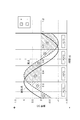
図7は、ノイズ成分の除去について説明する図である。図7(a)は励起光に起因する散乱光に応じた信号成分(ノイズ)の除去を行わなかった場合の検出光の強度、図7(b)は励起光に起因する散乱光に応じた信号成分(ノイズ)の除去を行った場合の検出光の強度を示している。図7(a)及び図7(b)において縦軸は検出光の強度を示しており、横軸は試料500の測定領域である測定部501における位置を示すチャンネルである。1チャンネルは例えば0.02mmである。図7(c)は、図7(a)及び図7(b)のチャンネルの位置に対応する試料500の領域を示す図である。図7(c)に示した試料500を拡大した模式図が図8である。図8に示されるように、試料500は、検体が滴下される滴下部502と、蛍光試薬で標識された検出抗体を保持する保持部503と、捕捉抗体を測定対象部504に固定した測定部501とが上流から下流に向けて配置されている。蛍光試薬は、例えばDTBTA-Eu3+である。測定部501は、例えば白色のイムノクロマトメンブレンの一部であるため、励起光を散乱し易い。
FIG. 7 is a diagram illustrating the removal of noise components. FIG. 7A shows the intensity of the detected light when the signal component (noise) corresponding to the scattered light caused by the excitation light is not removed, and FIG. 7B shows the intensity of the detected light according to the scattered light caused by the excitation light. It shows the intensity of the detected light when the signal component (noise) is removed. In FIGS. 7 (a) and 7 (b), the vertical axis represents the intensity of the detected light, and the horizontal axis represents the position in the
このような試料500に対して、滴下部502に検体を滴下すると、検体は毛細管現象により下流側へ移動する。検体中に被検出物質がある場合、保持部503の検出抗体と被検出物質とが反応して複合体を形成し、この複合体が測定部501を下流側に移動していく。そして、複合体が測定部501上の測定対象部504に達したときに、複合体が測定対象部504の捕捉抗体に捕捉され、被検出物質、検出抗体、及び捕捉抗体の3つによる複合体が形成される。この状態で測定領域である測定部501に対して集光位置(チャンネル)を変化させながら励起光が照射されることにより、図7(a)及び図7(b)に示されるようなチャンネル毎の検出光強度を導出することができる。図7(a)及び図7(b)において検出光強度が他と比べて大きくなっているチャンネルは、複合体が捕捉されている測定対象部504の位置に対応するチャンネルである。
When the sample is dropped onto the dropping
図7(a)に示されるように、散乱光に応じた信号成分(ノイズ)の除去が行われていない場合には、検出光には蛍光だけでなく散乱光が含まれるため、検出光強度が大きくなっている。そして、このようなノイズは励起光量を大きくすることに伴って大きくなるため、図7(a)に示されるように、励起光量を2倍にするとノイズも同様に2倍程度になっている。一般的にS/Nを向上させる方法として、励起光量を増加させることにより蛍光シグナル量を増加させる方法が考えられるが、上述したように、図7(a)のように励起光量に応じてノイズも増加する態様においては、S/Nを向上させることが難しい。さらに、励起光量を増加させることによってダイナミックレンジが狭まるという問題もある。 As shown in FIG. 7A, when the signal component (noise) corresponding to the scattered light is not removed, the detected light includes not only fluorescence but also scattered light, so that the detected light intensity Is getting bigger. Since such noise increases as the amount of excitation light increases, as shown in FIG. 7A, when the amount of excitation light is doubled, the noise also doubles. Generally, as a method of improving S / N, a method of increasing the amount of fluorescence signal by increasing the amount of excitation light can be considered, but as described above, noise is increased according to the amount of excitation light as shown in FIG. 7A. It is difficult to improve the S / N in the aspect of increasing. Further, there is a problem that the dynamic range is narrowed by increasing the amount of excitation light.
一方で、図7(b)に示されるように、散乱光に応じた信号成分(ノイズ)の除去を行った場合には、検出光には概ね蛍光のみが含まれており、検出したい信号(蛍光に基づく信号)のみを検出することができている。この場合には、ノイズがほぼ0であるため、図7(b)に示されるように、励起光量を増加させても(例えば2倍にしても)、光検出器が飽和しない限り、励起光(散乱光)の影響をほぼ0にキャンセルすることができ、ノイズが極端に大きくなることがない。以上のように、図7(b)に示されるようなノイズの除去を行う構成においては、励起光を増加させた場合にノイズ成分をほぼ0にキャンセルした状態でシグナル成分のみを増加させることができるため、S/Nの向上につながる。当該構成は、ノイズ成分に非常に強いため、励起光量を増加させることやIV変換アンプの増倍率を上げることが可能となる。 On the other hand, as shown in FIG. 7B, when the signal component (noise) corresponding to the scattered light is removed, the detected light generally contains only fluorescence, and the signal to be detected ( Only fluorescence-based signals) can be detected. In this case, since the noise is almost 0, as shown in FIG. 7B, even if the amount of excitation light is increased (for example, even if it is doubled), the excitation light is not saturated unless the photodetector is saturated. The influence of (scattered light) can be canceled to almost 0, and the noise does not become extremely large. As described above, in the configuration for removing noise as shown in FIG. 7B, when the excitation light is increased, only the signal component can be increased with the noise component canceled to almost 0. Since it can be done, it leads to improvement of S / N. Since this configuration is extremely resistant to noise components, it is possible to increase the amount of excitation light and increase the magnification of the IV conversion amplifier.
図9は、S/Nの定義について説明する図である。図9は、チャンネル毎の検出光の強度(測定領域の各位置における検出光の強度)の一例を示している。図9に示されるように、検出光の強度10count付近に±4程度のゆらぎ成分が存在している。このようなベース光量のゆらぎ(標準偏差)は、蛍光物質等が何も塗布されていない測定部501(或いは、計測状態と同様にぬれた状態とされた測定部501)に励起光をスキャンして取得される値である。以下では、当該ベース光量のゆらぎをノイズNと定義する。また、シグナルSは、「測定対象部504のピーク蛍光強度から全チャネルにおける測定対象部504の位置を除いたノイズ成分の平均値を差し引いた値」と定義する。S/Nは、上記で定義したシグナルをノイズで割った値と定義する。
FIG. 9 is a diagram illustrating the definition of S / N. FIG. 9 shows an example of the intensity of the detected light for each channel (intensity of the detected light at each position in the measurement region). As shown in FIG. 9, a fluctuation component of about ± 4 exists in the vicinity of the detection light intensity of 10 count. For such fluctuations (standard deviation) in the amount of base light, the excitation light is scanned into the measuring unit 501 (or the measuring
なお、図9に示される例では、ノイズの値が10countほどオフセットしている。後述するキャリブレーション処理を行うことによって、原理的にはノイズの値はほぼ0にキャンセルされる。しかし、ノイズの値に応じたバックグラウンドはばらつきがあるところ、ソフトでの解析の観点からは信号が常にプラスの値となることが好ましいため、バックグラウンドのオフセット処理を行っている。なお、オフセット量は、信号がダイナミックレンジ内(0〜4096count内)に収まるように設定される。オフセット量は、ダイナミックレンジの観点から極力少なくしつつ、測定部501に励起光をスキャンすることにより得られるバックグラウンドの信号が常に(ほぼ確実に)プラスの値となるように設定されている。具体的には、オフセット量は、例えば、蛍光物質等が何も塗布されていない測定部501(或いは、計測状態と同様にぬれた状態とされた測定部501)に励起光をスキャンして取得される検出光の強度平均値+該強度平均値の6σの値とされてもよい。なお、回路系に突発的なノイズが飛び込んでくる場合に備えて、上記で計算されるオフセット量に適当なマージンを加えて最終的なオフセット量とされてもよい。オフセット量は、ダイナミックレンジを犠牲にせず且つ信号がマイナスに出力されないように選択され、例えば+20count程度であってもよい。
In the example shown in FIG. 9, the noise value is offset by about 10 counts. In principle, the noise value is canceled to almost 0 by performing the calibration process described later. However, since the background varies depending on the noise value, it is preferable that the signal always has a positive value from the viewpoint of software analysis, so the background offset processing is performed. The offset amount is set so that the signal falls within the dynamic range (0 to 4096 count). The offset amount is set so that the background signal obtained by scanning the excitation light in the measuring
次に、散乱光に応じた信号成分(ノイズ)の除去手法について、具体的に説明する。光学測定装置1では、ロックイン回路であるキャンセル回路60においてキャリブレーション処理が行われ、該キャリブレーション処理の実施結果が考慮されて、検出信号から散乱光に応じた信号成分(ノイズ)が除去される。
Next, a method for removing signal components (noise) according to scattered light will be specifically described. In the
具体的には、光学測定装置1を用いた光学測定方法では、最初に、試料500とは異なるキャリブレーション処理用のリファレンス部材600(図15(a)参照)に励起光が照射されるように、照射光学系10の光学ヘッドが配置される。つづいて、照射光学系10からの励起光がリファレンス部材600に照射されることによる散乱光(リファレンス部材600において散乱した励起光成分)が検出光学系20の光検出素子21において検出される。ここで検出光学系20に検出される光は、基本的には、リファレンス部材600における蛍光を含まない散乱光のみの光であり、キャリブレーション処理に用いられるキャリブレーション処理用光である。
Specifically, in the optical measurement method using the
つづいて、キャリブレーション処理が実施される。具体的には、光学測定装置1のキャンセル回路60が、上述したキャリブレーション処理用光に応じたキャリブレーション信号に基づき、検出信号から散乱光に応じた信号成分を除去するためのキャリブレーション処理を実施する。キャリブレーション処理の詳細については後述する。そして、キャリブレーション処理の完了後、試料500の測定領域(測定部501)上を照射光学系10の光学ヘッドでスキャンすることにより、測定部501の蛍光情報が取得される。具体的には、キャンセル回路60が、上述したキャリブレーション処理の実施結果を考慮して、検出信号から散乱光に応じた信号成分を除去することにより、蛍光情報を取得する。
Subsequently, the calibration process is carried out. Specifically, the cancel
次に、キャリブレーション処理の詳細について説明する。光学測定装置1のキャンセル回路60は、例えばFPGA(Field Programmable Gate Array)を利用したロックイン回路である。キャリブレーション処理において、キャンセル回路60は、光源駆動回路30によって設定される光源11の変調周波数(例えばDDS(Direct Digital Synthesizer)の周波数)に合わせた、キャンセル回路60の動作周波数で周期を刻む周期信号に対して位相をずらしたロックイン用のスイッチ信号を生成する。そして、ロックイン回路として機能するキャンセル回路60は、測定信号であるキャリブレーショ信号、及び、参照信号であるスイッチ信号を入力として、散乱光に応じた信号成分を出力し、該散乱光に応じた信号成分の電圧値が0に近似する所定範囲内(スラッシュレベル)となるように、スイッチ信号の位相を調整する。
Next, the details of the calibration process will be described. The cancel
図10は、キャンセル回路60のFPGA内部でキャリブレーション処理に用いる信号を示している。図10に示される周期信号は、上述したようにDDSの周波数に合わせて周期を刻むクロック信号である。基準信号は、周期信号から任意の位相にある(周期信号に対して位相をずらした)、周期信号と同じ周波数の信号であり、後述するXY信号用のトリガである。XY信号は、上述したロックイン用のスイッチ信号であり、基準信号をトリガにして作られる信号である。X信号(第1信号)は、基準信号と位相差がない信号である。Y信号(第2信号)は、基準信号に対して90度位相がずれた信号である。キャンセル回路60は、実際にはX信号及びY信号に加えて、更に、X信号を反転させたX´信号(第3信号)と、Y信号を反転させたY´信号(第4信号)とを生成する。X信号、Y信号、X´信号、及びY´信号は、それぞれ独立した専用の回路によって生成される。散乱光に応じた信号成分の電圧値がスラッシュレベルとなるようにスイッチ信号の位相を調整するとは、すなわち、キャンセル回路60からの出力が0V(またはそれに近似する値)になるまで、周期信号に対して基準信号の位相をずらし続けることである。
FIG. 10 shows a signal used for the calibration process inside the FPGA of the cancel
図11は、周期信号に対して基準信号の位相をずらして出力が0Vになるように調整する処理を説明する図である。いま、周期信号、基準信号、及びスイッチ信号の初期状態の位相関係が図11(a)に示される状態であったとする。そして、スイッチ信号に基づいて図11中の網掛けの区間で積分処理がなされ、出力(散乱光に応じた信号成分の電圧値)がスラッシュレベルではなく且つ正の値であったとする。この場合、図11(b)に示されるように、スイッチ信号の位相を遅らせるように基準信号の位相が調整される。すなわち、キャンセル回路60は、キャリブレーション処理において、散乱光に応じた信号成分の電圧値がスラッシュレベルではなく正の値である場合には、スイッチ信号の位相を遅らせるように調整する。
FIG. 11 is a diagram illustrating a process of shifting the phase of the reference signal with respect to the periodic signal and adjusting the output so that the output becomes 0V. Now, it is assumed that the phase relationship of the periodic signal, the reference signal, and the switch signal in the initial state is the state shown in FIG. 11A. Then, it is assumed that the integration process is performed in the shaded section in FIG. 11 based on the switch signal, and the output (voltage value of the signal component corresponding to the scattered light) is not a slash level and is a positive value. In this case, as shown in FIG. 11B, the phase of the reference signal is adjusted so as to delay the phase of the switch signal. That is, in the calibration process, the cancel
いま、スイッチ信号の位相調整がなされた図11(b)の状態においても、網掛けの区間の積分処理の結果、出力(散乱光に応じた信号成分の電圧値)がスラッシュレベルではなく且つ正の値であったとする。この場合、図11(c)に示されるように、更にスイッチ信号の位相を遅らせるように基準信号の位相が調整される。 Now, even in the state of FIG. 11B in which the phase of the switch signal is adjusted, as a result of the integration processing of the shaded section, the output (voltage value of the signal component according to the scattered light) is not the slash level and is positive. It is assumed that the value is. In this case, as shown in FIG. 11C, the phase of the reference signal is adjusted so as to further delay the phase of the switch signal.
いま、スイッチ信号の位相調整がなされた図11(c)の状態においても、網掛けの区間の積分処理の結果、出力(散乱光に応じた信号成分の電圧値)がスラッシュレベルではなく且つ正の値であったとする。この場合、図11(d)に示されるように、更にスイッチ信号の位相を遅らせるように基準信号の位相が調整される。 Now, even in the state of FIG. 11C in which the phase of the switch signal is adjusted, the output (voltage value of the signal component according to the scattered light) is not a slash level and is positive as a result of the integration processing of the shaded section. It is assumed that the value is. In this case, as shown in FIG. 11D, the phase of the reference signal is adjusted so as to further delay the phase of the switch signal.
いま、スイッチ信号の位相調整がなされた図11(d)の状態において、網掛けの区間の積分処理の結果、出力(散乱光に応じた信号成分の電圧値)がスラッシュレベルではなく且つ負の値であったとする。この場合、図11(e)に示されるように、スイッチ信号の位相を進めるように基準信号の位相が調整される。すなわち、キャンセル回路60は、キャリブレーション処理において、散乱光に応じた信号成分の電圧値がスラッシュレベルではなく負の値である場合には、スイッチ信号の位相を進めるように調整する。
Now, in the state of FIG. 11D in which the phase of the switch signal is adjusted, as a result of the integration processing of the shaded section, the output (voltage value of the signal component according to the scattered light) is not a slash level and is negative. Suppose it was a value. In this case, as shown in FIG. 11E, the phase of the reference signal is adjusted so as to advance the phase of the switch signal. That is, in the calibration process, when the voltage value of the signal component corresponding to the scattered light is a negative value instead of the slash level, the cancel
そして、スイッチ信号の位相を進めるように調整された結果、図11(e)に示されるように、網掛けの区間の積分処理の結果、出力(散乱光に応じた信号成分の電圧値)がスラッシュレベル(0に近似する所定範囲内の値)になると、キャリブレーション処理が完了する。 Then, as a result of adjusting the phase of the switch signal so as to advance the phase, as shown in FIG. 11 (e), as a result of the integration processing of the shaded section, the output (voltage value of the signal component according to the scattered light) is obtained. When the slash level (a value within a predetermined range close to 0) is reached, the calibration process is completed.
キャリブレーション処理が完了すると、キャンセル回路60は、蛍光成分及び散乱光成分(励起光成分)を含んだ検出光に応じた検出信号と、キャリブレーション処理において位相が調整されたスイッチ信号とを入力として、検出信号から散乱光成分に応じた信号成分を除去する。
When the calibration process is completed, the cancel
図13は、キャリブレーション処理を示すフローチャートである。図13に示されるように、キャリブレーション処理では、最初に、AD変換器への入力が所定のオフセット電圧に切り替えられて0レベルが記憶される(ステップS11)。そして、スイッチの切り替えによりキャンセル回路60(ロックイン回路)の信号がAD変換器に入力される(ステップS12)。この状態で、一度強制的に基準信号の位相がずらされる(ステップS13)。キャンセル回路60(ロックイン回路)の出力は周期信号に対する基準信号の位相が0度と180度のときに0Vとなるが、初期状態で偶然180度に位相が合っていた場合、誤ってキャリブレーション処理を完了してしまい、出力される信号の正負が反転してしまうため、後段の回路の構成によっては出力される信号を検出できなくなる場合がある。この点、スタート時に強制的に基準信号の位相をずらすことにより、誤ってキャリブレーション処理が完了してしまうことを防止できる。また、このようにして開始時の位相を合わせることにより、出力される信号の正負が固定される。その結果、出力される信号をデジタル値に変換した際の符号ビットが必要なくなり、AD変換器のダイナミックレンジを有効に使用することができる。また、負の出力で計測したいときは、キャリブレーション完了の位相を0度ではなく180度にしてもよい。 FIG. 13 is a flowchart showing the calibration process. As shown in FIG. 13, in the calibration process, first, the input to the AD converter is switched to a predetermined offset voltage and the 0 level is stored (step S11). Then, the signal of the cancel circuit 60 (lock-in circuit) is input to the AD converter by switching the switch (step S12). In this state, the phase of the reference signal is forcibly shifted once (step S13). The output of the cancel circuit 60 (lock-in circuit) becomes 0V when the phase of the reference signal with respect to the periodic signal is 0 degrees and 180 degrees, but if the phase is accidentally matched to 180 degrees in the initial state, the calibration is erroneously performed. Since the processing is completed and the positive and negative of the output signal are inverted, the output signal may not be detected depending on the configuration of the circuit in the subsequent stage. In this respect, by forcibly shifting the phase of the reference signal at the start, it is possible to prevent the calibration process from being erroneously completed. Further, by matching the phase at the start in this way, the positive and negative of the output signal are fixed. As a result, the sign bit when the output signal is converted into a digital value is not required, and the dynamic range of the AD converter can be effectively used. Further, when it is desired to measure with a negative output, the phase of calibration completion may be set to 180 degrees instead of 0 degrees.
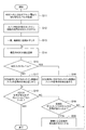
ステップS13が完了すると、現在のAD変換器の入力値が記録され(ステップS14)、キャリブレーションのループ処理が実行される。まず、現在のAD変換器の入力値と0レベルとが比較されて、AD変換器の入力値が0レベルよりも小さいか(負の値であるか)否かが判定される(ステップS15)。ステップS15においてAD変換器の入力値が負の値であると判定されると、DDSの周波数に応じた周期信号に対するキャンセル回路60のスイッチ信号(すなわち基準信号)の位相が進められる(ステップS16)。一方で、ステップS15においてAD変換器の入力値が正の値であると判定されると、周期信号に対するキャンセル回路60のスイッチ信号(すなわち基準信号)の位相が遅らされる(ステップS17)。
When step S13 is completed, the input value of the current AD converter is recorded (step S14), and the calibration loop process is executed. First, the input value of the current AD converter is compared with the 0 level, and it is determined whether or not the input value of the AD converter is smaller than the 0 level (negative value) (step S15). .. When it is determined in step S15 that the input value of the AD converter is a negative value, the phase of the switch signal (that is, the reference signal) of the cancel
そして、AD変換器の入力値について、符号が変化せずにスラッシュレベルとなったか否かが判定される(ステップS18)。ステップS18において符号が変化せずにスラッシュレベルになったと判定されると、キャリブレーション処理が終了する。一方で、ステップS18において条件を満たしていないと判定されると、位相をずらしたことによりAD変換器の入力の符号が変わったか否かが判定される(ステップS19)。ステップS19において変わっていないと判定された場合には再度ステップS14の処理が行われ、変わっていると判定された場合には制御による位相の変化幅が現状の半分に変更されて(ステップS20)、再度ステップS14の処理が行われる。以上が、キャリブレーション処理である。 Then, it is determined whether or not the input value of the AD converter has reached the slash level without changing the sign (step S18). When it is determined in step S18 that the sign does not change and the slash level is reached, the calibration process ends. On the other hand, if it is determined in step S18 that the condition is not satisfied, it is determined whether or not the sign of the input of the AD converter has changed due to the phase shift (step S19). If it is determined in step S19 that the phase has not changed, the process of step S14 is performed again, and if it is determined that the phase has not changed, the phase change width due to control is changed to half of the current state (step S20). , The process of step S14 is performed again. The above is the calibration process.
本態様では、蛍光を含まず散乱光を含むキャリブレーション処理用光を検出し、キャリブレーション処理用光に応じたキャリブレーション信号に基づき、検出信号から散乱光に応じた信号成分を除去するためのキャリブレーション処理を実施し、該キャリブレーション処理の実施結果を考慮して、検出信号から散乱光に応じた信号成分を除去する。検出信号から散乱光に応じた信号成分を除去するためのキャリブレーション処理を、散乱光を含むキャリブレーション処理用光に基づき予め行うことによって、検出信号から散乱光に応じた信号成分を適切に除去することができる。 In this embodiment, for detecting the calibration processing light containing scattered light without fluorescence, and removing the signal component corresponding to the scattered light from the detection signal based on the calibration signal corresponding to the calibration processing light. A calibration process is performed, and the signal component corresponding to the scattered light is removed from the detection signal in consideration of the execution result of the calibration process. By performing the calibration process for removing the signal component corresponding to the scattered light from the detection signal in advance based on the light for calibration processing including the scattered light, the signal component corresponding to the scattered light is appropriately removed from the detection signal. can do.
このようにして散乱光(ノイズ)を適切に除去することの効果について、図14を参照して説明する。図14(a)は散乱光に応じた信号成分(ノイズ)の除去を行わなかった場合の検出光の強度、図14(b)は散乱光に応じた信号成分(ノイズ)の除去を行った場合の検出光の強度を示している。図14は、蛍光試薬としてDTBTA-Eu3+を塗布したメンブレンを計測した場合の結果を示している。図14(a)に示されるように、ノイズの除去が行われていない場合においては、励起光(散乱光)のバックグラウンド(BKG)のために約330countsのオフセットが必要になっている。そして、ノイズ(標準偏差)は2.16、シグナル強度は404countsであった。これに対して、図14(b)に示されるように、ノイズの除去が行われている場合においては、励起光がメンブレンに散乱することを考慮したオフセットが必要とならず、ソフト上の処理(信号の値を全てプラスにする処理)のための最低限のオフセットのみが行われている。そして、ノイズ(標準偏差)は0.69、シグナル強度は1475countsとすることができた。このように、ノイズの除去が行われている場合においてはオフセット量が小さいため、光源からの励起光量及びIV変換アンプの増幅率を上げることができ、シグナル強度を好適に上げることができる。この結果、ノイズの除去が行われない場合のS/Nが187であるのにたいして、ノイズの除去が行われる場合のS/Nを2140とすることができ、S/Nを10倍以上向上させることができる。 The effect of appropriately removing scattered light (noise) in this way will be described with reference to FIG. FIG. 14 (a) shows the intensity of the detected light when the signal component (noise) corresponding to the scattered light was not removed, and FIG. 14 (b) shows the signal component (noise) removed according to the scattered light. It shows the intensity of the detected light in the case. FIG. 14 shows the results when the membrane coated with DTBTA-Eu 3+ as a fluorescent reagent was measured. As shown in FIG. 14A, when noise is not removed, an offset of about 330 counts is required due to the background (BKG) of the excitation light (scattered light). The noise (standard deviation) was 2.16 and the signal intensity was 404 counts. On the other hand, as shown in FIG. 14B, when noise is removed, an offset in consideration of scattering of excitation light on the membrane is not required, and processing on software is not required. Only the minimum offset for (processing to make all signal values positive) is performed. The noise (standard deviation) could be 0.69 and the signal intensity could be 1475 counts. As described above, when the noise is removed, the offset amount is small, so that the amount of excitation light from the light source and the amplification factor of the IV conversion amplifier can be increased, and the signal intensity can be preferably increased. As a result, the S / N when noise removal is not performed is 187, whereas the S / N when noise removal is performed can be 2140, which improves the S / N by 10 times or more. be able to.
キャリブレーション処理において、光源11の変調周波数に合わせたキャンセル回路60の動作周波数で周期を刻む周期信号に対して位相をずらしたロックイン用のスイッチ信号を生成し、キャリブレーション信号及びスイッチ信号を入力として、散乱光に応じた信号成分を出力し、該散乱光に応じた信号成分の電圧値が0に近似する所定範囲内となるように、スイッチ信号の位相を調整し、検出信号、及び、キャリブレーション処理において位相が調整されたスイッチ信号を入力として、検出信号から散乱光に応じた信号成分を除去してもよい。このように、ロックイン回路を用いて、キャリブレーション処理において散乱光に応じた信号成分の電圧値が0に近似する値となるようにスイッチ信号の位相が調整されることにより、位相調整後のスイッチ信号を入力として、検出信号から散乱光に応じた信号成分を適切に除去することができる。
In the calibration process, a lock-in switch signal that is out of phase with the periodic signal that ticks the period at the operating frequency of the cancel
キャリブレーション処理において、散乱光に応じた信号成分の電圧値が所定範囲内ではなく該所定範囲の値よりも大きい場合には、スイッチ信号の位相を遅らせるように調整し、散乱光に応じた信号成分の電圧値が所定範囲内ではなく該所定範囲の値よりも小さい場合には、スイッチ信号の位相を進めるように調整してもよい。これにより、キャリブレーション処理において散乱光に応じた信号成分の電圧値を、適切に0に近い値に調整することができる。 In the calibration process, if the voltage value of the signal component corresponding to the scattered light is not within the predetermined range but larger than the value in the predetermined range, the phase of the switch signal is adjusted so as to be delayed, and the signal corresponding to the scattered light is used. When the voltage value of the component is not within the predetermined range but smaller than the value in the predetermined range, the phase of the switch signal may be adjusted to advance. Thereby, in the calibration process, the voltage value of the signal component corresponding to the scattered light can be appropriately adjusted to a value close to 0.
光源11の変調周波数を、蛍光の強度がピーク値から1/eに落ちるまでの時間である蛍光寿命に対応する値よりも低くしてもよい。変調周波数が蛍光寿命に対応する値程度に高くされた場合には、連続する信号が互いに重なってしまう場合があり蛍光強度を最大化することができない。この点、変調周波数が蛍光寿命に対応する値よりも低くされることにより、蛍光強度を適切に高めることができる。
The modulation frequency of the
光源11の変調周波数を、蛍光寿命に対応する値よりも低く、且つ、商用周波数よりも高くしてもよい。これにより、変調周波数が蛍光寿命に対応する値よりも高くなり蛍光強度が弱まることを回避しながら、ノイズの増加を回避することができる。
The modulation frequency of the
ロックイン用のスイッチ信号として、X信号と、該X信号に対して位相が90度ずれたY信号と、X信号を反転させたX´信号と、Y信号を反転させたY´信号とを、それぞれ独立した専用の回路を用いて生成してもよい。独立した専用の回路で反転信号が生成されることにより、例えばnot回路により反転信号を生成する場合に問題となる微小な遅延(not回路の通過に伴う微小な遅延)が発生することを防止できる。 As the switch signal for lock-in, an X signal, a Y signal whose phase is 90 degrees out of phase with the X signal, an X'signal in which the X signal is inverted, and a Y'signal in which the Y signal is inverted are used. , Each may be generated using an independent dedicated circuit. By generating the inverting signal with an independent dedicated circuit, it is possible to prevent the occurrence of a minute delay (a minute delay due to the passage of the not circuit), which is a problem when the inverting signal is generated by the not circuit, for example. ..
キャンセル回路60(ロックイン回路)は、2種類の動作周波数が所定の割合で切り替えて設定されてもよい。これにより、動作周波数が1種類とされる場合よりも、ロックイン回路の動作周波数を光源11の変調周波数に合わせやすくなり、これらの同期制度を向上させることができる。
The cancel circuit 60 (lock-in circuit) may be set by switching between two types of operating frequencies at a predetermined ratio. As a result, it becomes easier to match the operating frequency of the lock-in circuit with the modulation frequency of the
キャリブレーション処理用光は、試料500における、測定対象部504に固定された捕捉抗体よりも下流側の領域に励起光が照射されることにより検出されてもよい。蛍光成分は捕捉抗体よりも上流側に滞留しやすいところ、補足抗体の下流側の領域に励起光が照射されてキャリブレーション処理用光が検出されることにより、適切に、蛍光成分の影響を低減したキャリブレーション処理用光を検出することができる。
The calibration processing light may be detected by irradiating the region downstream of the capture antibody fixed on the
次に、上述した蛍光測定におけるキャリブレーション処理の具体的な態様(第1〜第3の態様)について、図15〜図29を参照して説明する。各態様では、キャリブレーション処理方法が互いに異なっている。具体的には、第1の態様では、リファレンス部材に照射光を照射してキャリブレーション処理用光を検出することによりキャリブレーション処理を実施する。第2の態様では、検出光学系がキャリブレーション処理用光として照射光を直接検出することによりキャリブレーション処理を実施する。第3の態様では、疑似信号であるキャリブレーション信号を生成することによりキャリブレーション処理を実施する。なお、第1の態様の光学測定装置1(図1参照。すでに説明した構成)と、第2の態様の光学測定装置701(図23参照)及び第3の態様の光学測定装置801(図27参照)とは、互いに構成の一部が異なっている。以下、各態様について、詳細に説明する。
Next, specific aspects (first to third aspects) of the calibration process in the above-mentioned fluorescence measurement will be described with reference to FIGS. 15 to 29. In each aspect, the calibration processing methods are different from each other. Specifically, in the first aspect, the calibration process is performed by irradiating the reference member with the irradiation light and detecting the light for the calibration process. In the second aspect, the calibration process is performed by the detection optical system directly detecting the irradiation light as the light for the calibration process. In the third aspect, the calibration process is performed by generating a calibration signal which is a pseudo signal. The
[第1の態様]
図15は、第1の態様の蛍光測定手順について説明する図である。図15(a)に示されるように、第1の態様の蛍光測定では、最初に、照射光学系10の光源11が、測定対象物である試料500とは異なるキャリブレーション処理用のリファレンス部材600に照射光を照射し、検出光学系20の光検出素子21が、照射光が照射されたリファレンス部材600からの照射光の散乱光を含むキャリブレーション処理用光を検出する。そして、信号処理部であるキャンセル回路60(図1参照)が、キャリブレーション処理用光に応じたキャリブレーション信号に基づきキャリブレーション処理を実施する。以上が第1の態様における第1処理である。
[First aspect]
FIG. 15 is a diagram illustrating the fluorescence measurement procedure of the first aspect. As shown in FIG. 15A, in the fluorescence measurement of the first aspect, first, the
その後、図15(b)に示されるように、光源11が、測定対象物である試料500に励起光(照射光)を照射し、光検出素子21が、励起光が照射された試料500から生じる蛍光、及び、励起光が照射された試料500からの励起光の散乱光を含む測定対象光を検出する。そして、信号処理部であるキャンセル回路60(図1参照)が、キャリブレーション処理の実施結果を考慮し、測定対象光に応じた測定信号から散乱光に応じた信号成分を除去する。以上が第1の態様における第2処理である。図15(a)及び図15(b)を正面図とすると、図15(c)は右側面図である。図15(c)に示されるように、試料500からの蛍光を取得する際には、試料500の測定領域上を照射光学系10の光学ヘッドでスキャンすることにより、試料500の測定対象部504の蛍光情報が取得される。
After that, as shown in FIG. 15B, the
このような蛍光測定は、より詳細には図18に示される構成によって実現されている。すなわち、最初にキャリブレーション処理が実施される場合には、サンプルステージに載置された試料500とは異なる位置、具体的には、固定部位602から略垂直に延びる固定部位601に固定されたリファレンス部材600に照射光が照射されるように、照射光学系10の光学ヘッドが配置される。そして、キャリブレーション処理が完了すると試料500に励起光(照射光)が照射されるように照射光学系10の光学ヘッドが移動し、試料500の測定対象部504の蛍光情報が取得されるように照射光学系10の光学ヘッドがスキャン動作を行う。
Such a fluorescence measurement is realized by the configuration shown in FIG. 18 in more detail. That is, when the calibration process is first performed, the reference is fixed at a position different from that of the
ここで、第1の態様におけるリファレンス部材600は、照射光を反射し、且つ、照射光の照射によりそれ自体が蛍光を発生しない部材であることが好ましい。なお、本願における、照射光の照射により蛍光を発生しないとは、照射光の照射によってもリファレンス部材600に起因する蛍光が発生しない、或いは、無視できる程度にしか蛍光を発生しないことを示す。一方、図16は蛍光を発生するリファレンス部材を用いた場合のキャリブレーションの効果について説明する図であり、図16(a)はあるリファレンス部材に照射光を照射する場合に検出される蛍光を含むキャリブレーション処理用光を示しており、図16(b)は図16(a)に示すキャリブレーション処理用光に係るキャリブレーション結果に基づく試料500の蛍光測定の結果を示している。図16(a)では、横軸に波長、縦軸に光強度が示されており、光検出器(光検出素子21)が検出可能な最低波長が破線で示されている。図16(b)では、横軸にチャンネル、縦軸に光強度が示されている。図16(a)には、ある蛍光を発生するリファレンス部材を380nmの照射光で励起した場合に、光検出素子21が検出可能な波長の蛍光、具体的には600〜850nm程度の蛍光が検出されていることが示されている。このように、蛍光を発生するリファレンス部材に照射光が照射された場合には、光検出素子21において散乱光(照射光)だけでなくリファレンス部材からの蛍光が検出されてしまう。すなわち、光検出素子21においては、蛍光を含むキャリブレーション処理用光が検出されてしまう。このような蛍光を含んだキャリブレーショ処理用光に基づいてキャリブレーション処理が行われる場合には、キャリブレーション信号を用いて、装置の出力の電圧値が0になるようにスイッチ信号の位相を調整する際に、スイッチ信号の位相が蛍光成分の影響を受けた位相に調整されてしまう(蛍光成分の位相にロックインしてしまう)。これにより、図16(b)に示されるように、キャリブレーション結果を考慮して試料500の蛍光測定を行うと、キャリブレーション処理時にリファレンス部材からの蛍光成分が除去(キャンセル)されるようにスイッチ信号が調整されている影響で、試料500からの蛍光の波形を取得できないおそれがある。図16(b)には、いずれのチャンネルにおいても試料500からの蛍光の波形が取得できていない例が示されている。
Here, it is preferable that the
図17は、対して、蛍光を発生しないリファレンス部材を用いた場合のキャリブレーションの効果について説明する図であり、図17(a)はあるリファレンス部材に照射光を照射する場合に検出されるキャリブレーション処理用光を示しており、図17(b)は図17(a)に示すキャリブレーション処理用光に係るキャリブレーション結果に基づく試料500の蛍光測定の結果を示している。図17(a)では、横軸に波長、縦軸に光強度が示されており、光検出器(光検出素子21)が検出可能な最低波長が破線で示されている。図17(b)では、横軸にチャンネル、縦軸に光強度が示されている。図17(a)には、ある蛍光を発生しないリファレンス部材に対して380nmの照射光を照射した場合において蛍光が検出されていない(或いは無視できる程度に微量しか検出されていない)ことが示されている。このように、キャリブレーション処理用光に蛍光が含まれておれず概ね散乱光のみが含まれている場合には、図17(b)に示されるように、キャリブレーション結果を考慮して試料500の蛍光計測を行うと、試料500からの散乱光に応じた信号成分のみが除去(キャンセル)されて、試料500からの蛍光の波形を適切に取得することができる。以上のことから、リファレンス部材600は、それ自体が蛍光を発生しない部材であることが好ましいと言える。
FIG. 17 is a diagram for explaining the effect of calibration when a reference member that does not generate fluorescence is used, and FIG. 17A is a calibration detected when a reference member is irradiated with irradiation light. The light for processing is shown, and FIG. 17 (b) shows the result of fluorescence measurement of the
つづいて、リファレンス部材600の一例として、図19〜図21に示される各例を説明する。図19は、リファレンス部材600としてミラー600Aを用いる場合の散乱光取得について説明する図である。図19に示されるように、リファレンス部材600はミラー600Aを含んでいてもよい。ミラー600Aは、照射光を反射することができるミラーであればどのようなミラーであってもよいが、より好ましくはミラー600Aが照射光の照射により蛍光を発生しない(ミラー600Aに起因する蛍光が発生しない、或いは、無視できる程度にしか蛍光を発生しない)材料から形成されるとより好ましい。ミラー600Aは、例えば表面が汚れにくいミラーであってもよい。ミラー600Aは、光源11から照射された照射光を反射する。ミラー600Aは、反射した照射光(散乱光)が光検出素子21に検出されるように、傾斜角度が調整されている。ミラー600Aは、調整機構(不図示)によって所定の傾斜角度に固定されている。光検出素子21に対するミラー600Aの傾斜角度が適切に調整されることにより、光検出素子21において検出される光量を大きくすることができる。
Subsequently, as an example of the
図20は、リファレンス部材600として反射拡散体600Bを用いる場合の散乱光取得について説明する図である。図20に示されるように、リファレンス部材600は反射拡散体600Bを含んでいてもよい。反射拡散体600Bは、例えば、それ自身が照射光の照射により蛍光を発生しない(反射拡散体600Bに起因する蛍光が発生しない、或いは、無視できる程度にしか蛍光を発生しない)材料から形成された部材であって、光検出素子21への入射光量が比較的安定する白色部材からなる反射拡散板である。反射拡散体600Bは、光源11から照射された照射光を様々な角度に拡散するように反射する。反射拡散体600Bは、反射した照射光(散乱光)が大きな光量で光検出素子21に検出される位置に配置されている。反射拡散体600Bは、例えば樹脂やセラミックからなる一体成型部材であるのが好ましいが、切削加工や複数部材の組み合わせ等により形成されていてもよく、例えば板状部材の表面に照射光を特定角度に散乱可能なフィルム等を設けることによって構成されていてもよい。
FIG. 20 is a diagram illustrating acquisition of scattered light when the
図21は、リファレンス部材600としてミラー611(反射基材)とすりガラス610(拡散体)とを用いる場合の散乱光取得について説明する図である。図21に示されるように、リファレンス部材600は照射光を透過するガラス部材であるすりガラス610及び照射光を反射するミラー611を含むリファレンス部材600Cを含んでいてもよい。リファレンス部材600Cにおいて、すりガラス610は、ミラー611に支持(積層)されるように設けられ、ミラー611よりも先に照射光が入射するように設けられている。すりガラス610は、例えば380nm以上の照射光を透過する材料で形成されており、表面(照射光の入射面)に凸凹状の凸凹部610aが形成されている。または、すりガラス610の表面に照射光を特定角度に散乱可能なフィルム等を設けてもよい。ミラー611は、照射光を反射するものであればよく、例えばアルミ等からなる板状金属部材や、アルミ等の金属膜でその表面を被覆した板状部材であり、すりガラス610を収容するように箱状の部材としてもよい。また、ミラー611及びすりガラス610は、ともに照射光の照射により蛍光を発生しない(ミラー611及びすりガラス610に起因する蛍光が発生しない、或いは、無視できる程度にしか蛍光を発生しない)材料から形成されるとより好ましい。図21に示されるように、リファレンス部材600Cでは、すりガラス610に入射した照射光が凸凹部610aにおいて拡散しながらすりガラス610の内部を透過してミラー611に到達し、ミラー611において反射され、再度すりガラス610の内部を透過してすりガラス610の表面に到達し、その凸凹部610aにおいて様々な方向に拡散して出射される(様々な角度の散乱光が生じる)。様々な角度の散乱光が生じることによって、十分な光量の散乱光が光検出素子21において検出されることになる。なお、リファレンス部材600Cにおいては、表面が粗面化された反射材を用いてもよく、その場合、反射材の表面の粗面部が照射光を拡散する拡散体に相当する。
FIG. 21 is a diagram illustrating acquisition of scattered light when a mirror 611 (reflective base material) and frosted glass 610 (diffusing body) are used as the
次に、図22を参照して、第1の態様の蛍光測定処理を説明する。図22は、第1の態様の蛍光測定処理を示すフローチャートである。図22に示されるように、第1の態様の蛍光測定処理では、最初に、試料500とは異なるキャリブレーション処理用のリファレンス部材600に照射光が照射されるように照射光学系10の光学ヘッドが配置される(ステップS31。図15(a)参照)。そして、照射光が照射されたリファレンス部材600からの照射光の散乱光を含むキャリブレーション処理用光が光検出素子21において検出される(ステップS32。図15(a)参照)。そして、キャンセル回路60において、キャリブレーション処理用光に応じたキャリブレーション信号に基づき、検出信号から散乱光に応じた信号成分を除去するためのキャリブレーション処理が実施される(ステップS33)。キャリブレーション処理の詳細については、図10〜図13等を参照して上述したとおりであるので、説明を省略する。
Next, with reference to FIG. 22, the fluorescence measurement process of the first aspect will be described. FIG. 22 is a flowchart showing the fluorescence measurement process of the first aspect. As shown in FIG. 22, in the fluorescence measurement process of the first aspect, first, the optical head of the irradiation
つづいて、試料500の測定エリア領域を照射光学系10の光学ヘッドがスキャンするように動作して試料500の測定対象部504に励起光(照射光)が照射されることにより(ステップS34。図15(c)参照)、励起光が照射された試料500から生じる蛍光及び励起光が照射された試料500からの励起光の散乱光を含む測定対象光が光検出素子21において検出される(ステップS35。図15(b)参照)。そして、キャンセル回路60において、ステップS33のキャリブレーション処理の実施結果に基づいて、上述した測定対象光に応じた測定信号から散乱光に応じた信号成分が除去される(ステップS36)。具体的には、上述したように、キャンセル回路60は、測定信号とキャリブレーション処理において位相が調整されたスイッチ信号とを入力として、測定信号から散乱光に応じた信号成分を除去する。
Subsequently, the optical head of the irradiation
次に、第1の態様に係る作用効果について説明する。 Next, the action and effect according to the first aspect will be described.
第1の態様に係る光学測定装置1は、照射対象に照射光(励起光)を照射する照射光学系10と、照射光(励起光)に起因する検出光を検出する検出光学系20と、検出光に応じた検出信号を処理するキャンセル回路60とを備えている。そして、光学測定装置1では、第1処理において、照射光学系10が、試料500とは異なるキャリブレーション処理用のリファレンス部材600を照射対象として該リファレンス部材600に照射光を照射し(図15(a)参照)、検出光学系20が、照射光が照射されたリファレンス部材600からの照射光の散乱光を含むキャリブレーション処理用光を検出光として検出し(図15(a)参照)、キャンセル回路60が、キャリブレーション処理用光に応じたキャリブレーション信号を検出信号として、キャリブレーション信号に基づき、後述する第2処理における検出信号から散乱光に応じた信号成分を除去するためのキャリブレーション処理を実施する。また、光学測定装置1では、第2処理において、照射光学系10が、試料500を照射対象として、試料500に励起光(照射光)を照射し(図15(b)参照)、検出光学系20が、励起光が照射された試料500から生じる蛍光、及び、励起光が照射された試料500からの散乱光を含む測定対象光を検出光として検出し(図15(b)参照)、キャンセル回路60が、測定対象光に応じた測定信号を検出信号として、測定信号から、第1処理におけるキャリブレーション処理における散乱光に応じた信号成分を除去する。
The
このように、光学測定装置1では、キャリブレーション処理に係る第1処理において、試料500とは異なるリファレンス部材600に照射光が照射されて散乱光を含むキャリブレーション処理用光が検出されている。このことにより、例えば照射光の照射によっては蛍光を生じない(或いは、無視できる程度にしか蛍光を生じない)リファレンス部材600を準備することによって、蛍光を含まない(或いは、無視できる程度にしか蛍光を含まない)キャリブレーション処理用光を検出することが可能になる。このことで、第2処理において、キャリブレーション処理の実施結果に基づき、測定信号から散乱光に応じた信号成分のみを適切に除去することで、照射光自体に起因するノイズ成分を除去し、蛍光測定を高精度に行うことができる。また、試料500(実サンプル)とは異なる、キャリブレーション処理用のリファレンス部材600が用いられることにより、例えば実サンプルに照射光を照射してキャリブレーション処理用光を検出する場合に問題となる、実サンプルの特性(蛍光物質の移動速度等の違いによって決まる特性)に応じたキャリブレーション処理の結果のばらつきが生じない。より具体的には、実サンプルは例えば製造ロットの違いによる特性のばらつきがある場合があり、例えば蛍光物質の移動速度等といった違いが生じたりする場合がある。その場合、実サンプルごとに、キャリブレーション処理時において照射光が照射される領域エリアの蛍光物質量(つまり蛍光発光量)が互いに異なってしまう可能性がある。このことにより、キャリブレーション処理の結果が安定せず、例えば光学測定の結果の判定に十分な信頼性が得られないおそれがあるが、リファレンス部材600が用いられることにより、蛍光測定をより高精度に行うことができる。こまた、実サンプルごとの特性の違いに応じて装置が出力する結果が異なる場合には、例えばイムノクロマト法を用いた測定において陽性・陰性判定をするための閾値の設定が難しくなるが、リファレンス部材600を用いてキャリブレーションを行う場合にはこのような問題も抑制することができる。また、例えば互いに形状の異なる複数の試料500(例えば各種抗原毎に個別に対応する複数のイムノクロマト試験片試薬キット)を1台の光学測定装置1で計測する場合においても、それぞれの試料500毎に適切なキャリブレーション領域を設定する必要がなく、キャリブレーション処理については1つのリファレンス部材600を用いて行うことができるため、ハード面での制御やソフト面での制御を単純化することができる。なお、例えば実サンプルに照射光を照射してキャリブレーション処理用光を検出する場合と比較しても、光学測定装置1自体の構成を大きく変化させる必要がないため、本態様はコストの点で優位である。また、実測値からキャリブレーション処理を行うため、本態様はキャリブレーション処理の精度を担保することができる(キャリブレーション処理において正確な位相合わせを行うことができる)。このように、本態様に係る光学測定装置1によれば、キャリブレーション処理をより適切に行うことができ、照射光自体に起因するノイズ成分をより適切に除去することで、照射光自体に起因するノイズ成分を除去し、蛍光測定を高精度に行うことができる。
As described above, in the
リファレンス部材600は、図19〜図21に示されるように照射光を反射する反射部材(ミラー600A、ミラー611、反射拡散体600B)を含んでいてもよい。このような構成によれば、検出光の光量を容易に大きくすることができる。さらに、反射部材は、照射光の照射により蛍光を発生しないのが好ましい。このような構成によれば、照射光の照射によっても、反射部材に起因する蛍光が発生しない(或いは、無視できる程度にしか蛍光を発生しない)ため、第2処理において、測定信号から散乱光成分に応じた信号成分のみを確実に除去することができる。
The
リファレンス部材600は、図20に示されるように、照射光を拡散する反射拡散体600Bを含んでいてもよい。このような構成によれば、反射拡散体600Bによって様々な角度の散乱光を容易に生じさせることができ、検出光の光量をより容易に大きくすることができる。また、このような構成では、リファレンス部材を単純な構成とすることができるため、加工性やコストの点で優位である。
As shown in FIG. 20, the
リファレンス部材600は、図21に示されるように、照射光を反射するミラー611と、ミラー611に支持され、照射光を拡散するすりガラス610を含んでいてもよい。このような構成によれば、ミラー611とガラス610との協働によって、検出光の光量をより容易に大きくすることができる。また、すりガラス610の表面には凸凹部610aが形成されているので、様々な角度の散乱光を容易に生じさせることができ、検出光の光量をより容易に大きくすることができる。
As shown in FIG. 21, the
リファレンス部材600は、図19に示されるように、ミラーを含んでいてもよい。このような構成によれば、光検出素子21に対するミラーの反射角度を調整することにより、検出光の光量をより容易に大きくすることができる。
The
[第2の態様]
図23は、第2の態様の光学測定装置701の概略構成図である。第2の態様の光学測定装置701は、上述した光学測定装置1(図1参照)と概ね同様の構成であるが、図23に示されるように、検出光学系720(第1の検出光学系)の光検出素子721を備えている点、及び、IV変換アンプ740を備えている点において、光学測定装置1と異なっている。光検出素子721は、検出光学系20(第2の検出光学系)の光検出素子21とは別の構成である。また、IV変換アンプ740は、IV変換アンプ40とは別の構成である。光検出素子721は、キャリブレーション処理に係る処理として、照射光学系10から照射される照射光(キャリブレーション処理用光)を検出光として直接検出する。光検出素子721は、検出光に応じた検出信号をIV変換アンプ740に出力する。IV変換アンプ740は、キャリブレーション処理に係る処理として、光検出素子721から入力された電力信号(検出信号)を電圧信号に変換する。IV変換アンプ740は、電圧信号に変換した検出信号を波形生成回路50に出力する。この場合、波形生成回路50は、IV変換アンプ740から入力された検出信号に基づいて、検出信号の波形を生成し、生成した波形(検出信号)の情報をキャンセル回路60に出力する。
[Second aspect]
FIG. 23 is a schematic configuration diagram of the
図24は、第2の態様における蛍光測定の概要を説明する図である。図24に示されるように、第2の態様の蛍光測定では、最初にキャリブレーション処理が実施される場合には、サンプルステージに載置された試料500とは異なる位置、具体的には、固定部位602から略垂直に延びる固定部位601に固定された光検出素子721に照射光が照射されるように、照射光学系10の光学ヘッドが配置される。このようにして照射光取得が行われることにより、照射光であるキャリブレーション処理用光が検出される。そして、キャリブレーション処理が完了すると試料500に励起光(照射光)が照射されるように照射光学系10の光学ヘッドが移動し、試料500の測定対象部504の蛍光情報が取得されるように照射光学系10の光学ヘッドがスキャン動作を行う。
FIG. 24 is a diagram illustrating an outline of fluorescence measurement in the second aspect. As shown in FIG. 24, in the fluorescence measurement of the second aspect, when the calibration process is first performed, the position different from that of the
図25は、第2の態様の励起光取得について説明する図である。図25(a)に示されるように、第2の態様の照射光取得では、照射光学系10の光源11が検出光学系720の光検出素子721に照射光を照射する。これにより、光検出素子721が、照射光であるキャリブレーション処理用光を直接検出する。そして、信号処理部であるキャンセル回路60が、キャリブレーション処理用光に応じたキャリブレーション信号に基づきキャリブレーション処理を実施する。照射光は散乱光と同じ位相を持つ光である。このため、光検出素子721が照射光をキャリブレーション処理用光として検出することによっても、検出信号から散乱光に応じた信号成分を除去するためのキャリブレーション処理を適切に行うことができる。なお、キャリブレーション処理後の処理(第2処理)については、第1の態様と同様であるので説明を省略する。
FIG. 25 is a diagram illustrating the acquisition of excitation light according to the second aspect. As shown in FIG. 25A, in the irradiation light acquisition of the second aspect, the
次に、図26を参照して、第2の態様の蛍光測定処理を説明する。図26は、第2の態様の蛍光測定処理を示すフローチャートである。図26に示されるように、第2の態様の蛍光測定処理では、最初に、試料500とは異なる位置に固定された光検出素子721に照射光が照射されるように照射光学系10の光学ヘッドが配置される(ステップS41。図25(a)参照)。そして、照射光であるキャリブレーション処理用光が光検出素子721において検出される(ステップS42。図25(a)参照)。当該照射光は、散乱光と同じ位相を持つ光である。そして、キャンセル回路60において、キャリブレーション処理用光に応じたキャリブレーション信号に基づき、検出信号から散乱光に応じた信号成分を除去するためのキャリブレーション処理が実施される(ステップS43)。キャリブレーション処理の詳細については、図10〜図13等を参照して上述したとおりであるので、説明を省略する。
Next, with reference to FIG. 26, the fluorescence measurement process of the second aspect will be described. FIG. 26 is a flowchart showing the fluorescence measurement process of the second aspect. As shown in FIG. 26, in the fluorescence measurement process of the second aspect, first, the optics of the irradiation
つづいて、試料500の測定領域上を照射光学系10の光学ヘッドがスキャンするように動作して試料500の測定対象部504に励起光(照射光)が照射されることにより(ステップS44)、励起光が照射された試料500から生じる蛍光及び励起光が照射された試料500からの励起光の散乱光を含む測定対象光が光検出素子21において検出される(ステップS45)。そして、キャンセル回路60において、上述した測定対象光に応じた測定信号から、ステップS43のキャリブレーション処理における散乱光に応じた信号成分が除去される(ステップS46)。具体的には、上述したように、キャンセル回路60は、測定信号とキャリブレーション処理において位相が調整されたスイッチ信号とを入力として、測定信号から散乱光に応じた信号成分を除去する。
Subsequently, the optical head of the irradiation
次に、第2の態様に係る作用効果について説明する。 Next, the action and effect according to the second aspect will be described.
第2の態様に係る光学測定装置701(図23参照)は、照射光(励起光)を照射する照射光学系10と、照射光(励起光)に起因する検出光を検出する検出光学系20及び検出光学系720を有する光検出部と、検出光に応じた検出信号を処理するキャンセル回路60と、を備えている。そして、光学測定装置701では、第1処理において、照射光学系10が、検出光学系720の光検出素子721に照射光を照射し、光検出素子721が、照射光であるキャリブレーション処理用光を検出光として検出し(図25(a)参照)、キャンセル回路60が、キャリブレーション処理用光に応じたキャリブレーション信号を検出信号として、該キャリブレーション信号に基づき、後述する第2処理における検出信号から散乱光に応じた信号成分を除去するためのキャリブレーション処理を実施する。また、光学測定装置701では、第2処理において、照射光学系10が、試料500に励起光(照射光)を照射し、検出光学系20が、励起光が照射された試料500から生じる蛍光、及び、励起光が照射された試料500からの散乱光を含む測定対象光を検出光として検出し、キャンセル回路60が、測定対象光に応じた測定信号を検出信号として、測定信号から、第1処理におけるキャリブレーション処理における散乱光に応じた信号成分を除去する。
The optical measuring device 701 (see FIG. 23) according to the second aspect includes an irradiation
このように、光学測定装置701では、キャリブレーション処理に係る第1処理において、検出光学系720の光検出素子721に対して直接照射光が照射されて、該照射光であるキャリブレーション処理用光が検出されている。照射光は、散乱光と同じ位相を持つ光である。このため、検出光学系720が照射光をキャリブレーション処理用光として検出することによって、蛍光を含まず且つ散乱光と同じ位相の光をキャリブレーション処理用光として適切に検出することが可能になる。このことで、第2処理において、キャリブレーション処理の実施結果に基づき、測定信号から散乱光に応じた信号成分を適切に除去することで、照射光自体に起因するノイズ成分を除去し、蛍光測定を高精度に行うことができる。また、試料500に照射光を照射せずにキャリブレーション処理用光が検出されるため、例えば試料500に照射光を照射してキャリブレーション処理用光を検出する場合に問題となる、試料500の特性に応じたキャリブレーション処理の結果のばらつきが生じない。より具体的には、実サンプルは例えば製造ロットの違いによる特性のばらつきがある場合があり、例えば蛍光物質の移動速度等といった違いが生じたりする場合がある。その場合、実サンプルごとに、キャリブレーション処理時において照射光が照射される領域エリアの蛍光物質量(つまり蛍光発光量)が互いに異なってしまう可能性がある。このことにより、キャリブレーション処理の結果が安定せず、例えば光学測定の結果の判定に十分な信頼性が得られないおそれがあるが、試料500に照射光を照射せずにキャリブレーション処理用光が検出されるため、蛍光測定をより高精度に行うことができる。また、実サンプルごとの特性の違いに応じて装置が出力する結果が異なる場合には、例えばイムノクロマト法を用いた測定において陽性・陰性判定をするための閾値の設定が難しくなるが、試料500に照射光を照射せずにキャリブレーション処理用光が検出される場合にはこのような問題も抑制することができる。また、例えば互いに形状の異なる複数の試料500(例えば各種抗原毎に個別に対応する複数のイムノクロマト試験片試薬キット)を1台の光学測定装置1で計測する場合においても、それぞれの試料500毎に適切なキャリブレーション領域を設定する必要がなく、キャリブレーション処理については、試料500に照射光を照射せずにキャリブレーション処理用光を検出することができるため、ハード面での制御やソフト面での制御を単純化することができる。また、照射光が直接検出されてキャリブレーション処理用光とされるため、キャリブレーション処理のための光量を十分に担保することができる。このように、本態様に係る光学測定装置701によれば、キャリブレーション処理をより適切に行うことができ、照射光自体に起因するノイズ成分をより適切に除去することで、照射光自体に起因するノイズ成分を除去し、蛍光測定を高精度に行うことができる。
As described above, in the
なお、上述した説明では、光学測定装置701が、第1の検出光学系である検出光学系720と第2の検出光学系である検出光学系20とを有しているとして説明したが、例えば、図25(b)に示されるように、光学測定装置が、第1の検出光学系及び第2の検出光学系として機能する1つの検出光学系820を備えていてもよい。検出光学系820は、光検出素子821を有している。この場合、照射光学系は、例えば、検出光学系820が第1の検出光学系(すなわち、照射光をキャリブレーション処理用光として検出する検出光学系)として機能する場合において検出光学系820に照射光を照射する照射光学系910と、検出光学系820が第2の検出光学系(すなわち、試料500からの蛍光及び散乱光を含む測定対象光を検出する検出光学系)として機能する場合において試料500に励起光(照射光)を照射する照射光学系10とを含んでいる。なお、この場合の照射光学系910の光源911及び照射光学系10の光源11は、いずれも基準信号に対して変調されている必要がある。
In the above description, it has been described that the
[第3の態様]
図27は、第3の態様の光学測定装置801の概略構成図である。第3の態様の光学測定装置801は、上述した光学測定装置1(図1参照)と概ね同様の構成であるが、図27に示されるように、遅延・増幅回路802を備えている点において光学測定装置1と異なっている。遅延・増幅回路802は、キャンセル回路60と共に信号処理部として機能する構成である。ここで、上述したように、光源駆動回路30は、タイミング生成器70から入力された基準となる周波数信号に基づいて光源11の変調周波数を設定している。遅延・増幅回路802は、タイミング生成器70から入力される周波数信号に基づいて、光源駆動回路30から光源11に設定される変調周波数の信号(変調信号)の位相を変化させた疑似信号(キャリブレーション信号)を生成する。
[Third aspect]
FIG. 27 is a schematic configuration diagram of the
具体的には、遅延・増幅回路802は、照射光学系10の光源11から照射された照射光の散乱光が検出光として検出光学系20に検出されるまでに相当する遅延に基づいて、上述した変調信号の位相を変化させた疑似信号(キャリブレーション信号)を生成する。このように、疑似信号は、キャリブレーション処理において、検出光学系20に検出される散乱光(照射光)を模擬した信号である。更に、遅延・増幅回路802は、照射光学系10の光源11から照射された照射光の散乱光が検出光として検出光学系20に検出される場合の振幅に基づいて疑似信号(キャリブレーション信号)の振幅を設定する。このように、遅延・増幅回路802は、光源11に設定される変調信号の位相及び振幅を加工した疑似信号を生成することにより、キャリブレーション処理用光を検出することなく(キャリブレーション処理のために光の照射及び検出を行うことなく)、キャリブレーション信号を得る。遅延・増幅回路802は、詳細には、位相を変化させるための遅延回路及び振幅を変化させるための増幅回路を有している。図28に示されるように、キャリブレーション処理のための光の照射等を行わないため、キャリブレーション処理を行う際の照射光学系10の光学ヘッドの位置は特に限定されない。なお、キャリブレーション処理後の処理(第2処理)については、第1の態様と同様であるので説明を省略する。
Specifically, the delay /
次に、図29を参照して、第3の態様の蛍光測定処理を説明する。図29は、第3の態様の蛍光測定処理を示すフローチャートである。図29に示されるように、第3の態様の蛍光測定処理では、最初に、遅延・増幅回路802において、照射光学系10の光源11から照射された照射光の散乱光が検出光として検出光学系20に検出されるまでに相当する遅延分だけ変調信号の位相を変化させた疑似信号(キャリブレーション信号)が生成される(ステップS51)。つづいて、キャンセル回路60において、疑似信号(キャリブレーション信号)に基づき、検出信号から散乱光に応じた信号成分を除去するためのキャリブレーション処理が実施される(ステップS52)。キャリブレーション処理の詳細については、図10〜図13等を参照して上述したとおりであるので、説明を省略する。
Next, with reference to FIG. 29, the fluorescence measurement process of the third aspect will be described. FIG. 29 is a flowchart showing the fluorescence measurement process of the third aspect. As shown in FIG. 29, in the fluorescence measurement process of the third aspect, first, in the delay /
つづいて、試料500の測定領域上を照射光学系10の光学ヘッドがスキャンするように動作して試料500の測定対象部504に励起光(照射光)が照射されることにより(ステップS53)、励起光が照射された試料500から生じる蛍光及び励起光が照射された試料500からの励起光の散乱光を含む測定対象光が光検出素子21において検出される(ステップS54)。そして、キャンセル回路60において、ステップS52のキャリブレーション処理の実施結果が考慮されて、上述した測定対象光に応じた測定信号から散乱光に応じた信号成分が除去される(ステップS55)。具体的には、上述したように、キャンセル回路60は、測定信号とキャリブレーション処理において位相が調整されたスイッチ信号とを入力として、測定信号から散乱光に応じた信号成分を除去する。
Subsequently, the optical head of the irradiation
次に、第3の態様に係る作用効果について説明する。 Next, the action and effect according to the third aspect will be described.
第3の態様に係る光学測定装置801(図27参照)は、変調信号に応じた照射光(励起光)を照射する照射光学系10と、照射光(励起光)に起因する検出光を検出する検出光学系20と、信号処理部として機能する遅延・増幅回路802及びキャンセル回路60と、を備えている。そして、光学測定装置801では、第1処理において、遅延・増幅回路802が、照射光学系10から照射された照射光の散乱光が検出光として検出光学系20に検出されるまでに相当する遅延を考慮して上記変調信号の位相を変化させた疑似信号(キャリブレーション信号)を生成し、キャンセル回路60が、疑似信号に基づき、第2処理における検出信号から散乱光に応じた信号成分を除去するためのキャリブレーション処理を実施する。また、光学測定装置801では、第2処理において、照射光学系10が、試料500に励起光(照射光)を照射し、検出光学系20が、励起光が照射された試料500から生じる蛍光、及び、励起光が照射された試料500からの散乱光を含む測定対象光を検出光として検出し、キャンセル回路60が、測定対象光に応じた測定信号を検出信号として、測定信号から、第1処理における前記キャリブレーション処理における散乱光に応じた信号成分を除去する。
The optical measuring device 801 (see FIG. 27) according to the third aspect detects the irradiation
このように、光学測定装置801では、キャリブレーション処理に係る第1処理において、照射光学系10に入力される変調信号の位相を照射光学系10の遅延に応じて変化させた疑似信号(キャリブレーション信号)が生成される。このように、照射光に係る変調信号について照射光学系10の遅延に応じたキャリブレーション信号が生成されることにより、キャリブレーション処理用光を検出することなく、実際に散乱光をキャリブレーション処理用光として検出した場合と同様のキャリブレーション信号(散乱光と同様の位相を持つキャリブレーション信号)を得ることができる。すなわち、このような構成によれば、蛍光の信号成分を含まない散乱光の信号成分のみのキャリブレーション信号を得ることができる。このことで、第2処理において、キャリブレーション処理の実施結果に基づき、測定信号から散乱光に応じた信号成分を適切に除去することで、照射光自体に起因するノイズ成分を除去し、蛍光測定を高精度に行うことができる。また、試料500に照射光を照射せずにキャリブレーション処理用光が検出されるため、例えば試料500に照射光を照射してキャリブレーション処理用光を検出する場合に問題となる、試料500の特性に応じたキャリブレーション処理の結果のばらつきが抑制される。より具体的には、実サンプルは例えば製造ロットの違いによる特性のばらつきがある場合があり、例えば蛍光物質の移動速度等といった違いが生じたりする場合がある。その場合、実サンプルごとに、キャリブレーション処理時において照射光が照射される領域エリアの蛍光物質量(つまり蛍光発光量)が互いに異なってしまう可能性がある。このことにより、キャリブレーション処理の結果が安定せず、例えば光学測定の結果の判定に十分な信頼性が得られないおそれがあるが、照射光に係る変調信号について照射光学系10遅延に応じたキャリブレーション信号が生成されることにより、蛍光測定をより高精度に行うことができる。また、実サンプルごとの特性の違いに応じて装置が出力する結果が異なる場合には、例えばイムノクロマト法を用いた測定において陽性・陰性判定をするための閾値の設定が難しくなるが、照射光に係る変調信号について照射光学系10遅延に応じたキャリブレーション信号が生成される場合にはこのような問題も抑制することができる。また、例えば互いに形状の異なる複数の試料500(例えば各種抗原毎に個別に対応する複数のイムノクロマト試験片試薬キット)を1台の光学測定装置1で計測する場合においても、それぞれの試料500毎に適切なキャリブレーション領域を設定する必要がなく、照射光に係る変調信号について照射光学系10遅延に応じたキャリブレーション信号が生成されるため、ハード面での制御やソフト面での制御を単純化することができる。また、実際にキャリブレーション処理用光を検出することなく電気的にキャリブレーション信号を生成するため、キャリブレーション処理用の検出光学系等が不要になり、シンプル且つ安価な装置構成とすることができる。このように、本態様に係る光学測定装置801によれば、キャリブレーション処理をより適切に行うことができ、照射光自体に起因するノイズ成分をより適切に除去し、蛍光測定をより高精度に行うことができる。
As described above, in the
さらに、上述した第1処理では、遅延・増幅回路802が、照射光学系10から照射された照射光の散乱光が検出光として検出光学系20に検出される場合の振幅を考慮してキャリブレーション信号の振幅を設定してもよい。これにより、散乱光をキャリブレーション処理用光として実際に検出する場合とより近似させたキャリブレーション信号を得ることができる。
Further, in the first process described above, the delay /
上述したようなキャリブレーション処理については、実際の計測における高い再現性を担保する上で、毎回同じ照射光量でキャリブレーション処理を行うことが好ましい。そのため、第1の態様等で説明した部材(リファレンス部材)を用いる場合には、該部材を機械的に安定して固定できることが好ましい。また、該部材は経時変化しにくいものが好ましい。また、第2の態様で説明したような、キャリブレーション処理に関して光検出素子に照射光を照射する場合においては、光源の光量を一定に保つために回路的にフィードバックすることが好ましい。なお、第3の態様のように疑似的に作り出した信号でキャリブレーション処理を行う態様においては、毎回同じ光量でキャリブレーションできると考えられる。 Regarding the calibration process as described above, it is preferable to perform the calibration process with the same amount of irradiation light each time in order to ensure high reproducibility in actual measurement. Therefore, when the member (reference member) described in the first aspect or the like is used, it is preferable that the member can be mechanically and stably fixed. Further, it is preferable that the member does not easily change with time. Further, in the case of irradiating the photodetector with the irradiation light for the calibration process as described in the second aspect, it is preferable to feed back in a circuit in order to keep the amount of light of the light source constant. In the embodiment in which the calibration process is performed using the pseudo-generated signal as in the third aspect, it is considered that the calibration can be performed with the same amount of light each time.
1,701,801…光学測定装置、10…照射光学系、20…検出光学系(光検出部,第2の検出光学系)、60…キャンセル回路(信号処理部)、600…リファレンス部材、600A…ミラー、600B…反射拡散体、610…すりガラス、611…ミラー、720…検出光学系(光検出部,第1の検出光学系)、802…遅延・増幅回路(信号処理部)、820…検出光学系(第1の検出光学系及び第2の検出光学系)、910…照射光学系。 1,701,801 ... Optical measuring device, 10 ... Irradiation optical system, 20 ... Detection optical system (light detection unit, second detection optical system), 60 ... Cancel circuit (signal processing unit), 600 ... Reference member, 600A ... Mirror, 600B ... Reflective diffuser, 610 ... Ground glass, 611 ... Mirror, 720 ... Detection optical system (light detection unit, first detection optical system), 802 ... Delay / amplification circuit (signal processing unit), 820 ... Detection Optical system (first detection optical system and second detection optical system), 910 ... Irradiation optical system.
Claims (9)
照射対象に照射光を照射する照射光学系と、
前記照射光に起因する検出光を検出する光検出部と、
前記検出光に応じた検出信号を処理する信号処理部と、を備え、
第1処理では、
前記照射光学系が、前記測定対象物とは異なるキャリブレーション処理用のリファレンス部材を前記照射対象として、前記リファレンス部材に前記照射光を照射し、
前記光検出部が、前記照射光が照射された前記リファレンス部材からの前記照射光の散乱光を含むキャリブレーション処理用光を前記検出光として検出し、
前記信号処理部が、前記キャリブレーション処理用光に応じたキャリブレーション信号を前記検出信号として、該キャリブレーション信号に基づき、第2処理における前記検出信号から散乱光に応じた信号成分を除去するためのキャリブレーション処理を実施し、
第2処理では、
前記照射光学系が、前記測定対象物を前記照射対象として、前記測定対象物に前記照射光を照射し、
前記光検出部が、前記照射光が照射された前記測定対象物から生じる蛍光、及び、前記照射光が照射された前記測定対象物からの散乱光を含む測定対象光を前記検出光として検出し、
前記信号処理部が、前記測定対象光に応じた測定信号を前記検出信号として、前記測定信号から、前記第1処理における前記キャリブレーション処理における前記散乱光に応じた信号成分を除去する、光学測定装置。 An optical measuring device that measures the optical characteristics of an object to be measured.
An irradiation optical system that irradiates the irradiation target with irradiation light,
A photodetector that detects the detection light caused by the irradiation light,
A signal processing unit that processes a detection signal according to the detection light is provided.
In the first process
The irradiation optical system irradiates the reference member with the irradiation light by using a reference member for calibration processing different from the measurement object as the irradiation target.
The light detection unit detects the calibration processing light including the scattered light of the irradiation light from the reference member irradiated with the irradiation light as the detection light.
The signal processing unit uses the calibration signal corresponding to the calibration processing light as the detection signal, and removes the signal component corresponding to the scattered light from the detection signal in the second processing based on the calibration signal. Calibration process of
In the second process
The irradiation optical system irradiates the measurement object with the irradiation light with the measurement object as the irradiation target.
The light detection unit detects the measurement target light including the fluorescence generated from the measurement target object irradiated with the irradiation light and the scattered light from the measurement target object irradiated with the irradiation light as the detection light. ,
Optical measurement in which the signal processing unit uses the measurement signal corresponding to the measurement target light as the detection signal and removes the signal component corresponding to the scattered light in the calibration process in the first process from the measurement signal. Device.
前記照射光を反射する反射基材と、
前記反射基材に支持され、前記照射光を拡散する拡散体と、を含んでいる、請求項2又は3記載の光学測定装置。 The reflective member is
A reflective base material that reflects the irradiation light and
The optical measuring apparatus according to claim 2 or 3, further comprising a diffuser supported by the reflective base material and diffusing the irradiation light.
照射光を照射する照射光学系と、
前記照射光に起因する検出光を検出する第1の検出光学系及び第2の検出光学系を有する光検出部と、
前記検出光に応じた検出信号を処理する信号処理部と、を備え、
第1処理では、
前記照射光学系が、前記第1の検出光学系に前記照射光を照射し、
前記光検出部の前記第1の検出光学系が、前記照射光であるキャリブレーション処理用光を前記検出光として検出し、
前記信号処理部が、前記キャリブレーション処理用光に応じたキャリブレーション信号を前記検出信号として、該キャリブレーション信号に基づき、第2処理における前記検出信号から散乱光に応じた信号成分を除去するためのキャリブレーション処理を実施し、
第2処理では、
前記照射光学系が、前記測定対象物に前記照射光を照射し、
前記光検出部の前記第2の検出光学系が、前記照射光が照射された前記測定対象物から生じる蛍光、及び、前記照射光が照射された前記測定対象物からの散乱光を含む測定対象光を前記検出光として検出し、
前記信号処理部が、前記測定対象光に応じた測定信号を前記検出信号として、前記測定信号から、前記第1処理における前記キャリブレーション処理における前記散乱光に応じた信号成分を除去する、光学測定装置。 An optical measuring device that measures the optical characteristics of an object to be measured.
Irradiation optical system that irradiates irradiation light and
A photodetector having a first detection optical system and a second detection optical system for detecting the detection light caused by the irradiation light, and
A signal processing unit that processes a detection signal according to the detection light is provided.
In the first process
The irradiation optical system irradiates the first detection optical system with the irradiation light.
The first detection optical system of the light detection unit detects the calibration processing light, which is the irradiation light, as the detection light.
The signal processing unit uses the calibration signal corresponding to the calibration processing light as the detection signal, and removes the signal component corresponding to the scattered light from the detection signal in the second processing based on the calibration signal. Calibration process of
In the second process
The irradiation optical system irradiates the measurement object with the irradiation light,
The second detection optical system of the photodetector is a measurement target including fluorescence generated from the measurement object irradiated with the irradiation light and scattered light from the measurement target irradiated with the irradiation light. Light is detected as the detection light,
Optical measurement in which the signal processing unit uses the measurement signal corresponding to the measurement target light as the detection signal and removes the signal component corresponding to the scattered light in the calibration process in the first process from the measurement signal. Device.
前記測定対象物とは異なるキャリブレーション処理用のリファレンス部材に照射光を照射することと、
前記照射光が照射された前記リファレンス部材からの前記照射光の散乱光を含むキャリブレーション処理用光を検出することと、
前記キャリブレーション処理用光に応じたキャリブレーション信号に基づき、測定信号から散乱光に応じた信号成分を除去するためのキャリブレーション処理を実施することと、
を含む第1処理と、
前記測定対象物に前記照射光を照射することと、
前記照射光が照射された前記測定対象物から生じる蛍光、及び、前記照射光が照射された前記測定対象物からの散乱光を含む測定対象光を検出することと、
前記測定対象光に応じた前記測定信号から、前記第1処理における前記キャリブレーション処理における前記散乱光に応じた信号成分を除去することと、
を含む第2処理と、を実行する光学測定方法。 An optical measurement method for measuring the optical characteristics of an object to be measured.
Irradiating a reference member for calibration processing different from the measurement object with irradiation light, and
Detection of calibration processing light including scattered light of the irradiation light from the reference member irradiated with the irradiation light, and
Based on the calibration signal corresponding to the calibration processing light, the calibration processing for removing the signal component corresponding to the scattered light from the measurement signal is performed.
The first process including
Irradiating the measurement object with the irradiation light and
To detect the fluorescence generated from the measurement target object irradiated with the irradiation light and the measurement target light including the scattered light from the measurement target object irradiated with the irradiation light.
From the measurement signal corresponding to the measurement target light, the signal component corresponding to the scattered light in the calibration process in the first process is removed.
A second process, including, and an optical measurement method for performing.
照射光を照射することと、
前記照射光であるキャリブレーション処理用光を検出することと、
前記キャリブレーション処理用光に応じたキャリブレーション信号に基づき、測定信号から散乱光に応じた信号成分を除去するためのキャリブレーション処理を実施することと、
を含む第1処理と、
前記測定対象物に前記照射光を照射することと、
前記照射光が照射された前記測定対象物から生じる蛍光、及び、前記照射光が照射された前記測定対象物からの散乱光を含む測定対象光を検出することと、
前記測定対象光に応じた前記測定信号から、前記第1処理における前記キャリブレーション処理における前記散乱光に応じた信号成分を除去することと、
を含む第2処理と、を実行する光学測定方法。 An optical measurement method for measuring the optical characteristics of an object to be measured.
Irradiating the irradiation light and
Detecting the calibration processing light, which is the irradiation light,
Based on the calibration signal corresponding to the calibration processing light, the calibration processing for removing the signal component corresponding to the scattered light from the measurement signal is performed.
The first process including
Irradiating the measurement object with the irradiation light and
To detect the fluorescence generated from the measurement target object irradiated with the irradiation light and the measurement target light including the scattered light from the measurement target object irradiated with the irradiation light.
From the measurement signal corresponding to the measurement target light, the signal component corresponding to the scattered light in the calibration process in the first process is removed.
A second process, including, and an optical measurement method for performing.
Priority Applications (8)
| Application Number | Priority Date | Filing Date | Title |
|---|---|---|---|
| JP2020066069A JP6931730B1 (en) | 2020-04-01 | 2020-04-01 | Optical measuring device and optical measuring method |
| EP21779692.9A EP4123291A4 (en) | 2020-04-01 | 2021-01-21 | Optical measurement device and optical measurement method |
| PCT/JP2021/002104 WO2021199605A1 (en) | 2020-04-01 | 2021-01-21 | Optical measurement device and optical measurement method |
| US17/914,434 US20230124819A1 (en) | 2020-04-01 | 2021-01-21 | Optical measurement device and optical measurement method |
| KR1020227031968A KR20220159971A (en) | 2020-04-01 | 2021-01-21 | Optical measuring device and optical measuring method |
| CN202180026082.5A CN115398210A (en) | 2020-04-01 | 2021-01-21 | Optical measurement device and optical measurement method |
| TW110109328A TW202141022A (en) | 2020-04-01 | 2021-03-16 | Optical measurement device and optical measurement method |
| JP2021132233A JP7348933B2 (en) | 2020-04-01 | 2021-08-16 | Optical measuring device and optical measuring method |
Applications Claiming Priority (1)
| Application Number | Priority Date | Filing Date | Title |
|---|---|---|---|
| JP2020066069A JP6931730B1 (en) | 2020-04-01 | 2020-04-01 | Optical measuring device and optical measuring method |
Related Child Applications (1)
| Application Number | Title | Priority Date | Filing Date |
|---|---|---|---|
| JP2021132233A Division JP7348933B2 (en) | 2020-04-01 | 2021-08-16 | Optical measuring device and optical measuring method |
Publications (2)
| Publication Number | Publication Date |
|---|---|
| JP6931730B1 true JP6931730B1 (en) | 2021-09-08 |
| JP2021162509A JP2021162509A (en) | 2021-10-11 |
Family
ID=77549888
Family Applications (2)
| Application Number | Title | Priority Date | Filing Date |
|---|---|---|---|
| JP2020066069A Active JP6931730B1 (en) | 2020-04-01 | 2020-04-01 | Optical measuring device and optical measuring method |
| JP2021132233A Active JP7348933B2 (en) | 2020-04-01 | 2021-08-16 | Optical measuring device and optical measuring method |
Family Applications After (1)
| Application Number | Title | Priority Date | Filing Date |
|---|---|---|---|
| JP2021132233A Active JP7348933B2 (en) | 2020-04-01 | 2021-08-16 | Optical measuring device and optical measuring method |
Country Status (7)
| Country | Link |
|---|---|
| US (1) | US20230124819A1 (en) |
| EP (1) | EP4123291A4 (en) |
| JP (2) | JP6931730B1 (en) |
| KR (1) | KR20220159971A (en) |
| CN (1) | CN115398210A (en) |
| TW (1) | TW202141022A (en) |
| WO (1) | WO2021199605A1 (en) |
Families Citing this family (1)
| Publication number | Priority date | Publication date | Assignee | Title |
|---|---|---|---|---|
| US20240066624A1 (en) | 2021-01-21 | 2024-02-29 | Tadatomo Suga | Bonding method, bonder, and bonding system |
Family Cites Families (14)
| Publication number | Priority date | Publication date | Assignee | Title |
|---|---|---|---|---|
| JPS613043A (en) * | 1984-06-18 | 1986-01-09 | Hitachi Ltd | Apparatus for determining base sequence of nucleic acid |
| WO1990009637A1 (en) * | 1989-02-13 | 1990-08-23 | Research Corporation Technologies, Inc. | Method and means for parallel frequency acquisition in frequency domain fluorometry |
| JPH04106470A (en) * | 1990-08-28 | 1992-04-08 | Hitachi Ltd | Particulate immune measurement method and apparatus |
| US5270548A (en) * | 1992-07-31 | 1993-12-14 | The United States Of America As Represented By The United States Department Of Energy | Phase-sensitive flow cytometer |
| JPH1151856A (en) * | 1997-08-07 | 1999-02-26 | Nippon Telegr & Teleph Corp <Ntt> | Method for measuring photoreflectance mapping |
| WO1999026186A1 (en) * | 1997-11-19 | 1999-05-27 | University Of Washington | High throughput optical scanner |
| JP2010518394A (en) | 2007-02-06 | 2010-05-27 | ナンヤン・テクノロジカル・ユニバーシティー | Apparatus and method for analyzing a fluorescent sample placed on a substrate |
| US7630072B2 (en) * | 2007-06-20 | 2009-12-08 | Carestream Health, Inc. | Fluorescence calibrator for multiple band flat field correction |
| JP5094484B2 (en) * | 2008-03-11 | 2012-12-12 | 富士フイルム株式会社 | Fluorescence detection method and fluorescence detection apparatus |
| US20100032582A1 (en) | 2008-08-07 | 2010-02-11 | General Electric Company | Fluorescence detection system and method |
| JP5487150B2 (en) | 2011-03-31 | 2014-05-07 | 富士フイルム株式会社 | Optical measuring method and optical measuring apparatus |
| JP2013200125A (en) | 2012-03-23 | 2013-10-03 | Mitsui Eng & Shipbuild Co Ltd | Fluorescence detector and fluorescence detection method |
| US10401605B2 (en) * | 2017-05-02 | 2019-09-03 | SCREEN Holdings, Co., Ltd. | Structured illumination in inverted light sheet microscopy |
| CN112912715A (en) * | 2018-10-25 | 2021-06-04 | 浜松光子学株式会社 | Optical measurement device and optical measurement method |
-
2020
- 2020-04-01 JP JP2020066069A patent/JP6931730B1/en active Active
-
2021
- 2021-01-21 US US17/914,434 patent/US20230124819A1/en active Pending
- 2021-01-21 EP EP21779692.9A patent/EP4123291A4/en active Pending
- 2021-01-21 KR KR1020227031968A patent/KR20220159971A/en unknown
- 2021-01-21 WO PCT/JP2021/002104 patent/WO2021199605A1/en unknown
- 2021-01-21 CN CN202180026082.5A patent/CN115398210A/en active Pending
- 2021-03-16 TW TW110109328A patent/TW202141022A/en unknown
- 2021-08-16 JP JP2021132233A patent/JP7348933B2/en active Active
Also Published As
| Publication number | Publication date |
|---|---|
| JP2021179447A (en) | 2021-11-18 |
| EP4123291A1 (en) | 2023-01-25 |
| JP2021162509A (en) | 2021-10-11 |
| TW202141022A (en) | 2021-11-01 |
| EP4123291A4 (en) | 2024-04-24 |
| WO2021199605A1 (en) | 2021-10-07 |
| US20230124819A1 (en) | 2023-04-20 |
| KR20220159971A (en) | 2022-12-05 |
| JP7348933B2 (en) | 2023-09-21 |
| CN115398210A (en) | 2022-11-25 |
Similar Documents
| Publication | Publication Date | Title |
|---|---|---|
| JP7021288B2 (en) | Optical measuring device and optical measuring method | |
| WO2021199605A1 (en) | Optical measurement device and optical measurement method | |
| JP2006133178A (en) | Measuring device | |
| TW200844439A (en) | Method for measuring immunochromato test piece | |
| JP2001194305A (en) | Device for fluorescence correlative spectroscopic analysis | |
| WO2003038413A1 (en) | Apparatus for analyzing florescent image of biochip | |
| JP6923702B1 (en) | Optical measuring device and optical measuring method | |
| US20050231717A1 (en) | Fluorescence inspection spectrometer | |
| KR101774886B1 (en) | Autofocus immunochromatography sensitive detection system | |
| JP2001194303A (en) | Device for analyzing diffusion motion of fluorescent molecule | |
| JP2010091428A (en) | Scanning optical system | |
| JP2000206047A (en) | Spectrum-measuring device | |
| JP2022519845A (en) | Sample analysis methods, analyzers and computer programs | |
| JPH09229883A (en) | Dark field type photothermal transduction spectrometer | |
| JPH08334317A (en) | Measuring microscope | |
| EP3998470A1 (en) | Detection device and detection method | |
| JPH10186241A (en) | Darkfield down illumination microscope device | |
| JP3956315B2 (en) | Apparatus for adjusting fluorescence detection apparatus, method for adjusting fluorescence detection apparatus, and manufacturing method | |
| JPH11133152A (en) | Light distance measuring apparatus | |
| JP2009518642A (en) | Sensors with improved signal-to-noise ratio and accuracy | |
| CN101241027A (en) | Method and device for determining photo-electric devices micro-zone light reflection spectrum | |
| JPH085927A (en) | Confocal microscope | |
| JP2012132854A (en) | Analyzer and analytic method | |
| JP2007065077A (en) | Microscope |
Legal Events
| Date | Code | Title | Description |
|---|---|---|---|
| A521 | Request for written amendment filed |
Free format text: JAPANESE INTERMEDIATE CODE: A523 Effective date: 20210608 |
|
| A621 | Written request for application examination |
Free format text: JAPANESE INTERMEDIATE CODE: A621 Effective date: 20210608 |
|
| A871 | Explanation of circumstances concerning accelerated examination |
Free format text: JAPANESE INTERMEDIATE CODE: A871 Effective date: 20210608 |
|
| TRDD | Decision of grant or rejection written | ||
| A01 | Written decision to grant a patent or to grant a registration (utility model) |
Free format text: JAPANESE INTERMEDIATE CODE: A01 Effective date: 20210803 |
|
| A61 | First payment of annual fees (during grant procedure) |
Free format text: JAPANESE INTERMEDIATE CODE: A61 Effective date: 20210816 |
|
| R150 | Certificate of patent or registration of utility model |
Ref document number: 6931730 Country of ref document: JP Free format text: JAPANESE INTERMEDIATE CODE: R150 |