JP6929282B2 - Time-based delay line analog-to-digital converter - Google Patents
Time-based delay line analog-to-digital converter Download PDFInfo
- Publication number
- JP6929282B2 JP6929282B2 JP2018523813A JP2018523813A JP6929282B2 JP 6929282 B2 JP6929282 B2 JP 6929282B2 JP 2018523813 A JP2018523813 A JP 2018523813A JP 2018523813 A JP2018523813 A JP 2018523813A JP 6929282 B2 JP6929282 B2 JP 6929282B2
- Authority
- JP
- Japan
- Prior art keywords
- digital
- circuit
- current
- delay
- delay line
- Prior art date
- Legal status (The legal status is an assumption and is not a legal conclusion. Google has not performed a legal analysis and makes no representation as to the accuracy of the status listed.)
- Active
Links
Images


Classifications
-
- H—ELECTRICITY
- H03—ELECTRONIC CIRCUITRY
- H03M—CODING; DECODING; CODE CONVERSION IN GENERAL
- H03M1/00—Analogue/digital conversion; Digital/analogue conversion
- H03M1/004—Reconfigurable analogue/digital or digital/analogue converters
- H03M1/007—Reconfigurable analogue/digital or digital/analogue converters among different resolutions
-
- H—ELECTRICITY
- H03—ELECTRONIC CIRCUITRY
- H03M—CODING; DECODING; CODE CONVERSION IN GENERAL
- H03M1/00—Analogue/digital conversion; Digital/analogue conversion
- H03M1/12—Analogue/digital converters
- H03M1/34—Analogue value compared with reference values
-
- H—ELECTRICITY
- H02—GENERATION; CONVERSION OR DISTRIBUTION OF ELECTRIC POWER
- H02M—APPARATUS FOR CONVERSION BETWEEN AC AND AC, BETWEEN AC AND DC, OR BETWEEN DC AND DC, AND FOR USE WITH MAINS OR SIMILAR POWER SUPPLY SYSTEMS; CONVERSION OF DC OR AC INPUT POWER INTO SURGE OUTPUT POWER; CONTROL OR REGULATION THEREOF
- H02M3/00—Conversion of dc power input into dc power output
- H02M3/02—Conversion of dc power input into dc power output without intermediate conversion into ac
- H02M3/04—Conversion of dc power input into dc power output without intermediate conversion into ac by static converters
- H02M3/10—Conversion of dc power input into dc power output without intermediate conversion into ac by static converters using discharge tubes with control electrode or semiconductor devices with control electrode
- H02M3/145—Conversion of dc power input into dc power output without intermediate conversion into ac by static converters using discharge tubes with control electrode or semiconductor devices with control electrode using devices of a triode or transistor type requiring continuous application of a control signal
- H02M3/155—Conversion of dc power input into dc power output without intermediate conversion into ac by static converters using discharge tubes with control electrode or semiconductor devices with control electrode using devices of a triode or transistor type requiring continuous application of a control signal using semiconductor devices only
- H02M3/156—Conversion of dc power input into dc power output without intermediate conversion into ac by static converters using discharge tubes with control electrode or semiconductor devices with control electrode using devices of a triode or transistor type requiring continuous application of a control signal using semiconductor devices only with automatic control of output voltage or current, e.g. switching regulators
-
- H—ELECTRICITY
- H03—ELECTRONIC CIRCUITRY
- H03K—PULSE TECHNIQUE
- H03K5/00—Manipulating of pulses not covered by one of the other main groups of this subclass
- H03K5/13—Arrangements having a single output and transforming input signals into pulses delivered at desired time intervals
- H03K5/131—Digitally controlled
-
- H—ELECTRICITY
- H03—ELECTRONIC CIRCUITRY
- H03K—PULSE TECHNIQUE
- H03K5/00—Manipulating of pulses not covered by one of the other main groups of this subclass
- H03K5/13—Arrangements having a single output and transforming input signals into pulses delivered at desired time intervals
- H03K5/14—Arrangements having a single output and transforming input signals into pulses delivered at desired time intervals by the use of delay lines
-
- H—ELECTRICITY
- H03—ELECTRONIC CIRCUITRY
- H03M—CODING; DECODING; CODE CONVERSION IN GENERAL
- H03M1/00—Analogue/digital conversion; Digital/analogue conversion
- H03M1/10—Calibration or testing
- H03M1/1009—Calibration
-
- H—ELECTRICITY
- H03—ELECTRONIC CIRCUITRY
- H03M—CODING; DECODING; CODE CONVERSION IN GENERAL
- H03M1/00—Analogue/digital conversion; Digital/analogue conversion
- H03M1/10—Calibration or testing
- H03M1/1009—Calibration
- H03M1/1028—Calibration at two points of the transfer characteristic, i.e. by adjusting two reference values, e.g. offset and gain error
-
- H—ELECTRICITY
- H03—ELECTRONIC CIRCUITRY
- H03M—CODING; DECODING; CODE CONVERSION IN GENERAL
- H03M1/00—Analogue/digital conversion; Digital/analogue conversion
- H03M1/10—Calibration or testing
- H03M1/1009—Calibration
- H03M1/1033—Calibration over the full range of the converter, e.g. for correcting differential non-linearity
- H03M1/1057—Calibration over the full range of the converter, e.g. for correcting differential non-linearity by trimming, i.e. by individually adjusting at least part of the quantisation value generators or stages to their nominal values
-
- H—ELECTRICITY
- H03—ELECTRONIC CIRCUITRY
- H03M—CODING; DECODING; CODE CONVERSION IN GENERAL
- H03M1/00—Analogue/digital conversion; Digital/analogue conversion
- H03M1/10—Calibration or testing
- H03M1/1071—Measuring or testing
-
- H—ELECTRICITY
- H03—ELECTRONIC CIRCUITRY
- H03M—CODING; DECODING; CODE CONVERSION IN GENERAL
- H03M1/00—Analogue/digital conversion; Digital/analogue conversion
- H03M1/12—Analogue/digital converters
- H03M1/18—Automatic control for modifying the range of signals the converter can handle, e.g. gain ranging
-
- H—ELECTRICITY
- H03—ELECTRONIC CIRCUITRY
- H03M—CODING; DECODING; CODE CONVERSION IN GENERAL
- H03M1/00—Analogue/digital conversion; Digital/analogue conversion
- H03M1/12—Analogue/digital converters
- H03M1/34—Analogue value compared with reference values
- H03M1/38—Analogue value compared with reference values sequentially only, e.g. successive approximation type
-
- H—ELECTRICITY
- H03—ELECTRONIC CIRCUITRY
- H03K—PULSE TECHNIQUE
- H03K5/00—Manipulating of pulses not covered by one of the other main groups of this subclass
- H03K2005/00013—Delay, i.e. output pulse is delayed after input pulse and pulse length of output pulse is dependent on pulse length of input pulse
- H03K2005/00019—Variable delay
- H03K2005/00058—Variable delay controlled by a digital setting
-
- H—ELECTRICITY
- H03—ELECTRONIC CIRCUITRY
- H03M—CODING; DECODING; CODE CONVERSION IN GENERAL
- H03M1/00—Analogue/digital conversion; Digital/analogue conversion
- H03M1/12—Analogue/digital converters
- H03M1/50—Analogue/digital converters with intermediate conversion to time interval
- H03M1/502—Analogue/digital converters with intermediate conversion to time interval using tapped delay lines
Description
(優先権)
本願は、各々が2016年4月12日に出願された米国仮出願第62/321,668号、62/321,685号、62/321,687号,62/321,694号に対する優先権を主張するものであり、これらは、全体が参照により本明細書中に援用される。
(priority)
This application gives priority to US Provisional Applications 62 / 321,668, 62 / 321,685, 62 / 321,687, 62 / 321,694, each filed on April 12, 2016. Allegedly, these are incorporated herein by reference in their entirety.
(技術分野)
本開示は、時間ベースの遅延ラインアナログ・デジタルコンバータ(ADC)に関し、特に、背景較正、レンジ調節、およびレンジ外推定を伴う、そのようなコンバータに関する。
(Technical field)
The present disclosure relates to time-based delay line analog-to-digital converters (ADCs), especially those with background calibration, range adjustment, and out-of-range estimation.
多くの異なる種類のADCが、存在し、その使用は、多くの場合、用途に依存する。ADCは、ビットサイズに従って変動し得、アナログ信号は、2nの異なるデジタル値にデジタル化され、ADCは、nビットコンバータであって、nビットを使用して、アナログ値のレンジを表すであろう。さらに、ADCは、アナログ信号のための入力レンジを含み得る。ADCの最低デジタル化出力(例えば、8ビットADCに関しては00000000)は、アナログ信号入力の下限に対応し得る。ADCの最高デジタル化出力(例えば、8ビットADCに関しては11111111)は、アナログ信号入力の上限に対応し得る。そのような例示的値は、正または符号なし値を規定し得るが、2の補数バイナリ列挙が、代わりに使用されてもよい。ADCは、サンプリングレート、すなわち、アナログ信号がサンプリングされる頻度に対応し得る、定義された帯域幅を有し得る。ADCは、可変線形度に従って、値を出力し得る。 There are many different types of ADCs, and their use is often application dependent. The ADC can vary according to the bit size, the analog signal is digitized to 2 n different digital values, and the ADC is an n-bit converter, using n bits to represent the range of analog values. Let's go. In addition, the ADC may include an input range for analog signals. The lowest digitized output of the ADC (eg, 000000000 for an 8-bit ADC) may correspond to the lower bound of the analog signal input. The highest digitized output of the ADC (eg, 11111111 for an 8-bit ADC) may correspond to the upper limit of the analog signal input. Such exemplary values may specify positive or unsigned values, but a two's complement binary enumeration may be used instead. The ADC may have a defined bandwidth that can correspond to the sampling rate, i.e., how often the analog signal is sampled. The ADC may output values according to variable linearity.
本開示の実施形態は、差動デジタル遅延ラインと、差動デジタル遅延ライン内に含まれる遅延要素のセットを備える、第1の回路と、差動デジタル遅延ライン内に含まれる遅延要素の別のセットを備える、第2の回路とを含む、差動デジタル遅延ラインADCを含む。前述の実施形態のいずれかと組み合わせて、第1の回路は、入力のアナログ・デジタル変換を表すデータを発生させるように構成される。前述の実施形態のいずれかと組み合わせて、第2の回路は、差動デジタル遅延ラインへのソースを較正するように構成される。前述の実施形態のいずれかと組み合わせて、第1の回路は、入力電圧と基準電圧との間の差異を測定するように構成される。前述の実施形態のいずれかと組み合わせて、ADCは、差動デジタル遅延ラインのそれぞれへの基準電流を反映するように構成される、電流ソース回路を含む。前述の実施形態のいずれかと組み合わせて、電流ソース回路は、差動デジタル遅延ラインのそれぞれへの基準電流を反映するように構成され、第2の回路は、基準電流を調節し、誤差を最小限にするように構成される。前述の実施形態のいずれかと組み合わせて、ADCは、入力差動電圧を差動電流に変換するように構成される、トランスコンダクタを含み、第1の回路は、差動電流を測定し、差動電圧を表すデータを発生させるように構成される。前述の実施形態のいずれかと組み合わせて、ADCは、入力差動電圧を差動電流に変換し、複数の差動デジタル遅延ラインに基づいて、入力を受け取り、電圧・電流レンジを調節するように構成される、トランスコンダクタを含む。前述の実施形態のいずれかと組み合わせて、各差動デジタル遅延ラインは、電流限定バッファ鎖を含む。前述の実施形態のいずれかと組み合わせて、所与の差動デジタル遅延ラインが、所与の差動デジタル遅延ラインに適用される差動電流に従って、ある速度で動作するように構成される。前述の実施形態のいずれかと組み合わせて、ADCはさらに、より高速の差動デジタル遅延ラインの完了に応じて、より低速の差動デジタル遅延ラインからのデータを保存するように構成される、ラッチを含む。前述の実施形態のいずれかと組み合わせて、ADCは、差動デジタル遅延ライン内に含まれる遅延要素のさらに別のセットを備える、第3の回路を含み、第3の回路は、ADCへの入力が入力レンジから外れている程度を示すデータを生成するように構成される。前述の実施形態のいずれかと組み合わせて、ADCはさらに、デジタル遅延ラインの長さを相互から独立して調節することによりADCを較正する第3の回路を含む。前述の実施形態のいずれかと組み合わせて、ADCはさらに、相互から独立してデジタル遅延ラインの長さを調節することによりADCを較正する第3の回路を含み、第3の回路は、所与のデジタル遅延ラインを短くするかまたは長くするように所与のデジタル遅延ラインの一部分を選択的に使用するマルチプレクサを含む。 Embodiments of the present disclosure include a first circuit comprising a differential digital delay line and a set of delay elements contained within the differential digital delay line, and another of the delay elements contained within the differential digital delay line. Includes a differential digital delay line ADC, including a second circuit, including a set. In combination with any of the aforementioned embodiments, the first circuit is configured to generate data representing an analog-to-digital conversion of the input. In combination with any of the aforementioned embodiments, the second circuit is configured to calibrate the source to the differential digital delay line. In combination with any of the aforementioned embodiments, the first circuit is configured to measure the difference between the input voltage and the reference voltage. In combination with any of the aforementioned embodiments, the ADC includes a current source circuit configured to reflect a reference current to each of the differential digital delay lines. In combination with any of the aforementioned embodiments, the current source circuit is configured to reflect a reference current to each of the differential digital delay lines, and a second circuit adjusts the reference current to minimize error. Is configured to. In combination with any of the aforementioned embodiments, the ADC comprises a transformer configured to convert the input differential voltage into a differential current, the first circuit measuring the differential current and differential. It is configured to generate data representing voltage. In combination with any of the aforementioned embodiments, the ADC is configured to convert the input differential voltage to a differential current, receive the input and adjust the voltage / current range based on multiple differential digital delay lines. Includes transformers. In combination with any of the aforementioned embodiments, each differential digital delay line comprises a current limited buffer chain. In combination with any of the aforementioned embodiments, a given differential digital delay line is configured to operate at a certain speed according to the differential current applied to the given differential digital delay line. In combination with any of the aforementioned embodiments, the ADC is further configured to store data from the slower differential digital delay line upon completion of the faster differential digital delay line. include. In combination with any of the aforementioned embodiments, the ADC comprises a third circuit comprising yet another set of delay elements contained within the differential digital delay line, the third circuit having an input to the ADC. It is configured to generate data that indicates how far it is out of the input range. In combination with any of the aforementioned embodiments, the ADC further comprises a third circuit that calibrates the ADC by adjusting the length of the digital delay line independently of each other. In combination with any of the aforementioned embodiments, the ADC further comprises a third circuit that calibrates the ADC by adjusting the length of the digital delay line independently of each other, the third circuit being given. Includes a multiplexer that selectively uses a portion of a given digital delay line to shorten or lengthen the digital delay line.
本開示の実施形態は、差動デジタル遅延ラインと、差動デジタル遅延ライン内に含まれる遅延要素のセットを備える、第1の回路と、差動デジタル遅延ライン内に含まれる遅延要素の別のセットを備える、第2の回路とを含む、差動デジタル遅延ラインADCを含む。前述の実施形態のいずれかと組み合わせて、第1の回路は、入力のアナログ・デジタル変換を表すデータを発生させるように構成される。前述の実施形態のいずれかと組み合わせて、第2の回路は、ADCへの入力が入力レンジから外れている程度を示すデータを生成するように構成される。前述の実施形態のいずれかと組み合わせて、第1の回路は、入力電圧と基準電圧との間の差異を測定するように構成される。前述の実施形態のいずれかと組み合わせて、ADCは、差動デジタル遅延ラインのそれぞれへの基準電流を反映するように構成される、電流ソース回路を含む。前述の実施形態のいずれかと組み合わせて、ADCは、差動デジタル遅延ラインのそれぞれへの基準電流を反映するように構成される、電流ソース回路を含み、第2の回路は、基準電流を調節し、誤差を最小限にするように構成される。前述の実施形態のいずれかと組み合わせて、ADCは、入力差動電圧を差動電流に変換するように構成される、トランスコンダクタを含み、第1の回路は、差動電流を測定し、差動電圧を表すデータを発生させるように構成される。前述の実施形態のいずれかと組み合わせて、トランスコンダクタは、複数の差動デジタル遅延ラインに基づいて、入力を受け取り、電圧・電流レンジを調節するように構成される。前述の実施形態のいずれかと組み合わせて、各差動デジタル遅延ラインは、電流限定バッファ鎖を含む。前述の実施形態のいずれかと組み合わせて、所与の差動デジタル遅延ラインが、所与の差動デジタル遅延ラインに適用される差動電流に従って、ある速度で動作するように構成される。前述の実施形態のいずれかと組み合わせて、ADCはさらに、ラッチを備え、より高速の差動デジタル遅延ラインの完了に応じて、より低速の差動デジタル遅延ラインからのデータを保存するように構成される。前述の実施形態のいずれかと組み合わせて、ADCはさらに、差動デジタル遅延ライン内に含まれる遅延要素のさらに別のセットを備える、第3の回路を含み、第3の回路は、差動デジタル遅延ラインへのソースを較正するように構成される。前述の実施形態のいずれかと組み合わせて、ADCはさらに、デジタル遅延ラインの長さを相互から独立して調節することによりADCを較正する第3の回路を含む。前述の実施形態のいずれかと組み合わせて、ADCはさらに、デジタル遅延ラインの長さを相互から独立して調節することによりADCを較正する第3の回路を含み、第3の回路は、所与のデジタル遅延ラインを短くするかまたは長くするように所与のデジタル遅延ラインの一部分を選択的に使用するマルチプレクサを含む。 Embodiments of the present disclosure include a first circuit comprising a differential digital delay line and a set of delay elements contained within the differential digital delay line, and another of the delay elements contained within the differential digital delay line. Includes a differential digital delay line ADC, including a second circuit, including a set. In combination with any of the aforementioned embodiments, the first circuit is configured to generate data representing an analog-to-digital conversion of the input. In combination with any of the aforementioned embodiments, the second circuit is configured to generate data indicating the extent to which the input to the ADC is out of the input range. In combination with any of the aforementioned embodiments, the first circuit is configured to measure the difference between the input voltage and the reference voltage. In combination with any of the aforementioned embodiments, the ADC includes a current source circuit configured to reflect a reference current to each of the differential digital delay lines. In combination with any of the aforementioned embodiments, the ADC includes a current source circuit configured to reflect a reference current to each of the differential digital delay lines, a second circuit adjusting the reference current. , Configured to minimize error. In combination with any of the aforementioned embodiments, the ADC comprises a transformer configured to convert the input differential voltage into a differential current, the first circuit measuring the differential current and differential. It is configured to generate data representing voltage. In combination with any of the aforementioned embodiments, the transformer is configured to receive an input and adjust the voltage / current range based on a plurality of differential digital delay lines. In combination with any of the aforementioned embodiments, each differential digital delay line comprises a current limited buffer chain. In combination with any of the aforementioned embodiments, a given differential digital delay line is configured to operate at a certain speed according to the differential current applied to the given differential digital delay line. In combination with any of the aforementioned embodiments, the ADC is further configured to include a latch to store data from the slower differential digital delay line upon completion of the faster differential digital delay line. NS. In combination with any of the aforementioned embodiments, the ADC further comprises a third circuit comprising yet another set of delay elements contained within the differential digital delay line, the third circuit being the differential digital delay. It is configured to calibrate the source to the line. In combination with any of the aforementioned embodiments, the ADC further comprises a third circuit that calibrates the ADC by adjusting the length of the digital delay line independently of each other. In combination with any of the aforementioned embodiments, the ADC further comprises a third circuit that calibrates the ADC by adjusting the length of the digital delay line independently of each other, the third circuit being a given. Includes a multiplexer that selectively uses a portion of a given digital delay line to shorten or lengthen the digital delay line.
本開示の実施形態は、プロセッサと、マイクロコントローラと、電子デバイスと、ダイパッケージと、半導体パッケージと、前述の実施形態のADCのいずれかを含む、半導体デバイスとを含む。 Embodiments of the present disclosure include a processor, a microcontroller, an electronic device, a die package, a semiconductor package, and a semiconductor device including any of the ADCs of the aforementioned embodiments.
本開示の実施形態は、前述の実施形態のADCのいずれかによって行われる方法を含む。
本発明は、例えば、以下を提供する。
(項目1)
差動デジタル遅延ラインアナログ・デジタルコンバータ(ADC)であって、
複数の差動デジタル遅延ラインと、
前記差動デジタル遅延ライン内に含まれる遅延要素のセットを備える第1の回路と、
前記差動デジタル遅延ライン内に含まれる遅延要素の別のセットを備える第2の回路と
を備え、
前記第1の回路は、入力のアナログ・デジタル変換を表すデータを発生させるように構成され、
前記第2の回路は、前記差動デジタル遅延ラインへのソースを較正するように構成される、
ADC。
(項目2)
前記第1の回路は、入力電圧と基準電圧との間の差異を測定するように構成される、項目1または3−10のいずれかに記載のADC。
(項目3)
前記差動デジタル遅延ラインのそれぞれへの基準電流を反映するように構成される電流ソース回路をさらに備える、項目1−2または5−10のいずれかに記載のADC。
(項目4)
前記差動デジタル遅延ラインのそれぞれへの基準電流を反映するように構成される電流ソース回路をさらに備え、前記第2の回路は、前記基準電流を調節し、誤差を最小限にするように構成される、項目1−2または5−10のいずれかに記載のADC。
(項目5)
入力差動電圧を差動電流に変換するように構成されるトランスコンダクタをさらに備え、前記第1の回路は、前記差動電流を測定し、前記差動電圧を表すデータを発生させるように構成される、項目1−4または6−10のいずれかに記載のADC。
(項目6)
入力差動電圧を差動電流に変換することと、
前記複数の差動デジタル遅延ラインに基づいて、入力を受け取り、電圧・電流レンジを調節することと
を行うように構成される、トランスコンダクタ
をさらに備える、項目1−5または7−10のいずれかに記載のADC。
(項目7)
各差動デジタル遅延ラインは、電流限定バッファ鎖を含む、項目1−6または8−10のいずれかに記載のADC。
(項目8)
所与の差動デジタル遅延ラインが、前記所与の差動デジタル遅延ラインに適用される差動電流に従って、ある速度で動作するように構成され、
前記ADCはさらに、ラッチを備え、
前記ラッチは、より高速の差動デジタル遅延ラインの完了に応じて、より低速の差動デジタル遅延ラインからのデータを保存するように構成される、
項目1−7または9−10のいずれかに記載のADC。
(項目9)
前記差動デジタル遅延ライン内に含まれる遅延要素のさらに別のセットを備える第3の回路をさらに備え、前記第3の回路は、前記ADCへの入力が入力レンジから外れている程度を示すデータを生成するように構成される、項目1−8または10のいずれかに記載のADC。
(項目10)
相互から独立して前記デジタル遅延ラインの長さを調節することによって前記ADCを較正するための第4の回路をさらに備える、項目1−9のいずれかに記載のADC。
(項目11)
差動デジタル遅延ラインアナログ・デジタルコンバータ(ADC)であって、
複数の差動デジタル遅延ラインと、
前記差動デジタル遅延ライン内に含まれる遅延要素のセットを備える第1の回路と、
前記差動デジタル遅延ライン内に含まれる遅延要素の別のセットを備える第2の回路と
を備え、
前記第1の回路は、入力のアナログ・デジタル変換を表すデータを発生させるように構成され、
前記第2の回路は、前記ADCへの入力が入力レンジから外れている程度を示すデータを生成するように構成される、
ADC。
(項目12)
前記第1の回路は、入力電圧と基準電圧との間の差異を測定するように構成される、項目11または13−20のいずれかに記載のADC。
(項目13)
前記差動デジタル遅延ラインのそれぞれへの基準電流を反映するように構成される電流ソース回路をさらに備える、項目11−12または15−20のいずれかに記載のADC。
(項目14)
前記差動デジタル遅延ラインのそれぞれへの基準電流を反映するように構成される電流ソース回路をさらに備え、前記第2の回路は、前記基準電流を調節し、誤差を最小限にするように構成される、項目11−12または15−20のいずれかに記載のADC。
(項目15)
入力差動電圧を差動電流に変換するように構成されるトランスコンダクタをさらに備え、前記第1の回路は、前記差動電流を測定し、前記差動電圧を表すデータを発生させるように構成される、項目11−14または16−20のいずれかに記載のADC。
(項目16)
入力差動電圧を差動電流に変換することと、
前記複数の差動デジタル遅延ラインに基づいて、入力を受け取り、電圧・電流レンジを調節することと
を行うように構成される、トランスコンダクタ
をさらに備える、項目11−15または17−20のいずれかに記載のADC。
(項目17)
各差動デジタル遅延ラインは、電流限定バッファ鎖を含む、項目11−16または18−20のいずれかに記載のADC。
(項目18)
所与の差動デジタル遅延ラインが、前記所与の差動デジタル遅延ラインに適用される差動電流に従って、ある速度で動作するように構成され、
前記ADCはさらに、ラッチを備え、
前記ラッチは、より高速の差動デジタル遅延ラインの完了に応じて、より低速の差動デジタル遅延ラインからのデータを保存するように構成される、
項目11−17または19−20のいずれかに記載のADC。
(項目19)
前記差動デジタル遅延ライン内に含まれる遅延要素のさらに別のセットを備える第3の回路をさらに備え、前記第3の回路は、前記差動デジタル遅延ラインへのソースを較正するように構成される、項目11−18または20のいずれかに記載のADC。
(項目20)
相互から独立して前記デジタル遅延ラインの長さを調節することによって前記ADCを較正するための第4の回路をさらに備える、項目11−19のいずれかに記載のADC。
(項目21)
差動デジタル遅延ラインアナログ・デジタルコンバータ(ADC)であって、
複数の差動デジタル遅延ラインと、
前記差動デジタル遅延ライン内に含まれる遅延要素のセットを備える第1の回路と、
トランスコンダクタであって、
入力差動電圧を差動電流に変換することと、
前記複数の差動デジタル遅延ラインに基づいて、入力を受け取り、電圧・電流レンジを調節することと
を行うように構成される、トランスコンダクタと
を備える、ADC。
(項目22)
前記差動デジタル遅延ライン内に含まれる遅延要素のさらに別のセットを備える、第2の回路をさらに備え、前記第2の回路は、前記ADCへの入力が入力レンジから外れている程度を示すデータを生成するように構成される、項目21に記載のADC。
(項目23)
項目1−22に記載のADCのいずれかを備える、マイクロコントローラ。
(項目24)
項目1−22に記載のADCの構成のいずれかの動作を含む、方法。
Embodiments of the present disclosure include methods performed by any of the ADCs of the aforementioned embodiments.
The present invention provides, for example,:
(Item 1)
Differential digital delay line analog-to-digital converter (ADC)
With multiple differential digital delay lines,
A first circuit comprising a set of delay elements contained within the differential digital delay line.
With a second circuit comprising another set of delay elements contained within the differential digital delay line
With
The first circuit is configured to generate data representing an analog-to-digital conversion of the input.
The second circuit is configured to calibrate the source to the differential digital delay line.
ADC.
(Item 2)
The ADC according to any one of
(Item 3)
The ADC according to any one of items 1-2 or 5-10, further comprising a current source circuit configured to reflect a reference current to each of the differential digital delay lines.
(Item 4)
It further comprises a current source circuit configured to reflect a reference current to each of the differential digital delay lines, the second circuit being configured to adjust the reference current and minimize errors. The ADC according to any one of items 1-2 or 5-10.
(Item 5)
Further comprising a transformer configured to convert the input differential voltage into a differential current, the first circuit is configured to measure the differential current and generate data representing the differential voltage. The ADC according to any one of items 1-4 or 6-10.
(Item 6)
Converting the input differential voltage to a differential current and
To receive the input and adjust the voltage / current range based on the multiple differential digital delay lines.
Constructed to do
The ADC according to any one of items 1-5 or 7-10, further comprising.
(Item 7)
The ADC according to any of items 1-6 or 8-10, wherein each differential digital delay line comprises a current limited buffer chain.
(Item 8)
A given differential digital delay line is configured to operate at a certain speed according to the differential current applied to the given differential digital delay line.
The ADC further comprises a latch.
The latch is configured to store data from a slower differential digital delay line upon completion of a faster differential digital delay line.
The ADC according to any of items 1-7 or 9-10.
(Item 9)
The third circuit further comprises a third circuit comprising yet another set of delay elements contained within the differential digital delay line, the third circuit being data indicating the extent to which the input to the ADC is out of the input range. The ADC according to any one of items 1-8 or 10, wherein the ADC is configured to generate.
(Item 10)
The ADC according to any one of items 1-9, further comprising a fourth circuit for calibrating the ADC by adjusting the length of the digital delay line independently of each other.
(Item 11)
Differential digital delay line analog-to-digital converter (ADC)
With multiple differential digital delay lines,
A first circuit comprising a set of delay elements contained within the differential digital delay line.
With a second circuit comprising another set of delay elements contained within the differential digital delay line
With
The first circuit is configured to generate data representing an analog-to-digital conversion of the input.
The second circuit is configured to generate data indicating the extent to which the input to the ADC is out of the input range.
ADC.
(Item 12)
The ADC according to any one of items 11 or 13-20, wherein the first circuit is configured to measure a difference between an input voltage and a reference voltage.
(Item 13)
The ADC according to any one of items 11-12 or 15-20, further comprising a current source circuit configured to reflect a reference current to each of the differential digital delay lines.
(Item 14)
It further comprises a current source circuit configured to reflect a reference current to each of the differential digital delay lines, the second circuit being configured to adjust the reference current and minimize errors. The ADC according to any of items 11-12 or 15-20.
(Item 15)
Further comprising a transformer configured to convert the input differential voltage into a differential current, the first circuit is configured to measure the differential current and generate data representing the differential voltage. The ADC according to any of items 11-14 or 16-20.
(Item 16)
Converting the input differential voltage to a differential current and
To receive the input and adjust the voltage / current range based on the multiple differential digital delay lines.
Constructed to do
The ADC according to any one of items 11-15 or 17-20, further comprising.
(Item 17)
The ADC according to any of items 11-16 or 18-20, wherein each differential digital delay line comprises a current limited buffer chain.
(Item 18)
A given differential digital delay line is configured to operate at a certain speed according to the differential current applied to the given differential digital delay line.
The ADC further comprises a latch.
The latch is configured to store data from a slower differential digital delay line upon completion of a faster differential digital delay line.
The ADC according to any of items 11-17 or 19-20.
(Item 19)
It further comprises a third circuit comprising yet another set of delay elements contained within the differential digital delay line, the third circuit being configured to calibrate the source to the differential digital delay line. The ADC according to any one of items 11-18 or 20.
(Item 20)
The ADC according to any of items 11-19, further comprising a fourth circuit for calibrating the ADC by adjusting the length of the digital delay line independently of each other.
(Item 21)
Differential digital delay line analog-to-digital converter (ADC)
With multiple differential digital delay lines,
A first circuit comprising a set of delay elements contained within the differential digital delay line.
Transconductor
Converting the input differential voltage to a differential current and
To receive the input and adjust the voltage / current range based on the multiple differential digital delay lines.
Configured to do, with a transformer
The ADC.
(Item 22)
It further comprises a second circuit comprising yet another set of delay elements contained within the differential digital delay line, the second circuit indicating the extent to which the input to the ADC is out of the input range. 21. The ADC of item 21, which is configured to generate data.
(Item 23)
A microcontroller comprising any of the ADCs of item 1-22.
(Item 24)
A method comprising the operation of any of the ADC configurations according to item 1-22.
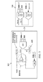
図1は、本開示の実施形態による、例示的オーバーレンジ保護可変分解能差動遅延ラインADC100を図示する。 FIG. 1 illustrates an exemplary overrange protection variable resolution differential delay line ADC100 according to an embodiment of the present disclosure.
ADC100は、例えば、スイッチモード電源システム(SMPS)において使用されてもよい。SMPS制御ループは、アナログ値の測定を利用し得る。制御ループは、高速1実行サイクル測定を要求し得る。単一サイクル内でADC100によって測定された値の読取およびそれへの作用は、SMPSの安定性および効率を改良し得る。故に、ADC100の超高速実装が、必要とされ得る。ADC100の速度は、ランタイムの間、パルス幅変調(PWM)サイクルの間のPWMコマンドを更新するために、ADC100の分解能に影響を及ぼし得る。
The
ADC100は、デジタル遅延ライン(DDL)ADCとして実装されてもよい。デジタル遅延ラインADCとしての実装を通して、ADC100は、従来のフラッシュADCより低いコストかつより少ない電力でその測定を行い得る。一実施形態では、ADC100は、背景較正を含んでもよい。別の実施形態では、ADC100は、レンジ調節を含んでもよい。さらに別の実施形態では、ADC100は、そのアナログ入力が測定されるであろう所望のレンジから外れている程度を推定してもよい。背景較正またはレンジ調節を組み込むことは、性能および機能性を改良する。ADC100の誤差電圧がレンジを超えると、ADC100を使用する制御ループがロックを再取得することが、困難になり得る。ADC100によって作成されたレンジ外推定値は、アルゴリズムが必要な調節を行い得るように、方向および誤差の定質的推定値を提供する。推定値が、ADCの正確なレンジ外であっても、推定値が正確なレンジ外にある程度のみの定質的推定値は、より良好な作用および性能を可能にし得る。
The
ADC100は、主に、デジタル低電圧論理を用いて実装され得る。故に、ADC100は、占有面積またはダイサイズに関して小型であり得る。さらに、ADC100は、したがって、低電力を要求し得る。また、ADC100は、したがって、非常に高速で動作し得る。故に、ADC100は、SMPS制御ループ内の誤差計算ADCとして使用されてもよい。
The
背景較正は、分解能および正確度等の重要なメトリックに関してADC100性能を改良し得る。レンジ調節は、SMPS制御ループをより柔軟にし、システムADC100が実装される必要があるシステムに適合可能にし得る。レンジ外推定は、ADC100がその線形レンジ外にあるとき(その入力に対して)、有用な情報を提供し得る。さらに、ADC100は、推定の一部として、レンジ外入力の定質的または定量的大きさおよび符号または方向を規定し得る。
Background calibration can improve ADC100 performance with respect to important metrics such as resolution and accuracy. Range adjustment may make the SMPS control loop more flexible and adaptable to the system in which the system ADC100 needs to be implemented. Out-of-range estimation may provide useful information when the
ADC100を遅延ラインADCとして実装することによって、ADC100は、差動電圧を差動電流に変換し得る。図2は、本開示の実施形態による、入力回路200の表現を図示する。入力回路200は、ADC100とインターフェースをとってもよい、またはADC100の一部として実装されてもよい。入力回路200は、入力電圧と基準電圧との間の差動電圧を電流に変換するように構成されてもよい。特に、入力回路200は、差動電圧をpbias電流およびnbias電流に変換し得る。入力回路200は、トランジスタのセットによって実装されてもよい。差動電流間の差異は、入力電圧と基準電圧との間の差動に関連する。pbias電流またはnbias電流のうちの一方は、他方より強いであろう。さらに、pbias電流またはnbias電流のうちの一方は、入力電圧または基準電圧がより高かった程度まで他方より強いであろう。
By mounting the
図1に戻ると、pbias電流およびnbias電流の出力は、入力102、104として適用され得る。ADC100は、電流スターブ型バッファ116、118を通してデータ遅延ラインとともに機能し得る。バッファ116、118の各要素は、個別のnbias102、pbias104電流からの電流が要素に到達すると、アクティブ化し、その入力を伝搬し得る。バッファ状態は、最初に、全てゼロであり得、伝搬されるべきconvert信号106は、1であり得る。他の場合には、バッファ状態は、最初に、全て1であり得、伝搬されるべきconvert信号106は、ゼロであり得る。バッファ116、118の各要素は、個別のnbias102、pbias104電流からの電流が要素に到達すると、アクティブ化し、その入力を伝搬することになるため、nbias102またはpbias104電流のより大きい、したがって、より高速の電流と関連付けられたバッファが、最初に満たされ得る。バッファは、convert信号106から伝搬される値で満たされ得る。他のバッファは、完全に満たされ得ないが、その電流の相対的速度(したがって、サイズ)に従って満たされ得る。故に、ADC100は、バッファ116、118のうちの1つの完了に応じて、バッファ116、118の不完全なバッファのステータスを検査し得る。部分的に満たされたバッファ内の満たされた要素の数に基づいて、nbias104およびpbias102間の相対的差異が、確認され得る。本相対的差異に基づいて、入力電圧と基準電圧との間の差異が、確認され得る。バッファ116、118は、バッファが、電流がpbias102またはnbias104から受信されるまでアクティブ化を待機するという点において、電流スターブ型バッファと称され得る。バッファ116、118は、個別の差動電流のサイズに関連する速度を用いて連続的にアクティブ化するであろう。
Returning to FIG. 1, the output of pbias current and nbias current can be applied as
ADC100は、サーモメータコードを通した各バッファ116、118の相対的速度を通して、pbias102とnbias104との間の速度の差異を表すように構成されてもよい。コードは、ラッチ112内に記憶され得る。ラッチ112は、第1のpbias102およびnbias104の完了に応じて、バッファ116、118のスナップショットとして、サーモメータコードを記憶し得る。第1のpbias102またはnbias102の完了に応じて、バッファ116、118の個別のバッファは、次の遅延要素への伝搬の代わりに、それぞれ、done+またはdone−になり得る、その信号を出力し得る。done+は、バッファ116が(pbias102に起因して)伝搬を終えたことを表し得、done−は、バッファ118が(nbias104に起因して)伝搬を終えたことを表し得る。ORゲートが、done+およびdone−を組み合わせ、done信号を発生させ得る。done信号は、ラッチ112の値を設定するための制御としてフィードされ得る。したがって、ラッチ112は、第1のバッファ116、118の完了に応じて生じるであろう、done信号が発生されると、その値を受け取り得る。設定または完了されたdone+およびdone−のうちの一方は、符号として保存され、差動の符号を示し得る。符号は、設定されるべきpsignおよびnsignによって表され得る。ラッチ112はまた、convert信号が発行されたかどうかに従って、設定またはリセットされ得る。
The
ラッチ112の値が設定されるべき時点で(nbias102またはpbias104がその個別のバッファの通過を終えたため)、バッファ116、118の本値は、ラッチ112の中にロードされ得る。一実施形態では、値の修正バージョンが、ラッチ112の中にロードされ得る。例えば、バッファ116、118の対応する要素からの値は、結果がラッチ112の対応する要素内に記憶される前に、NANDゲートをともに通過し得る。その結果、ラッチ112は、1のストリングに続いて、ゼロのストリングを記憶し得、1がゼロに切り替わる場所は、pbias102またはnbias104のより高速の方がその個別のバッファの端部に到達し、done信号を発生したときに、pbias102またはnbias104のより低速の方がその個別のバッファ内に到達した場所を表し得る。pbias102またはnbias104のより低速の方の本場所を示す、サーモメータコードは、サーモメータ内のシフトレジスタ、乗算器、または他のアルゴリズム回路によって、バイナリコンバータ114に変換され得る。結果として生じるデータ106は、pbias102とnbias104との間の相対的差異を示すために使用され得る。pbias102およびnbias104を発生した電圧の差異が、次いで、結果として生じるデータ106から推測され得る。いくつかの実施形態では、電圧調整器におけるように、本差異は、調整器の実際の出力電圧と調整器の出力電圧の所望のレベルとの間の差異であり得る。
At the time when the value of
ADC100は、デジタルセルを用いて実装される、バッファ116、118を含む。故に、ADC100は、小占有面積またはダイ要件および低電力を有し得る。ADC100は、したがって、他のADCより高速であり得る。さらに、DDLバッファを用いることにより、ADC100は、他の実装より小型であり得る。対照的に、従来のフラッシュADCとして実装されるADCは、高速であり得るが、現在のサブミクロン技術では、ノードは、大型であって、有意な電流を消費し得る。ADC100等の遅延ラインADCは、比較して、はるかに小型であって、電力がより少なくなり得る。
The
図3は、本開示の実施形態による、ADC100の典型的使用モデルを図示する。特に、302は、電圧調整器フィードバック判定におけるADCの使用を図示し、ADCは、本開示の教示を実装することができない。304は、本開示の教示による、電圧調整器フィードバックにおけるADC100の使用を図示する。
FIG. 3 illustrates a typical use model of the
302では、電圧感知(Vsense)は、電圧調整器によって出力された通りの電圧を感知し得る。本電圧は、基準電圧と比較されることになる。基準電圧は、所望の電圧基準レベルのアナログ信号を生成し得る、デジタル・アナログコンバータに適用される、制御ループコマンドコードによって規定され得る。Vsenseおよび基準電圧は、コンパレータに入力され得る。コンパレータはまた、別の電圧基準(Vbg)に接続され、符号付き誤差結果をサポートする、またはそれに適応し得る。Vbgはまた、ADC自体によって参照されてもよい。誤差は、ADCから出力され、基準電圧とVsenseとの間の制御ループ誤差を表し得る。 At 302, the voltage sensing (Vsense) may sense the voltage as output by the voltage regulator. This voltage will be compared with the reference voltage. The reference voltage can be specified by a control loop command code applied to the digital-to-analog converter that can produce an analog signal at the desired voltage reference level. The Vsense and reference voltage can be input to the comparator. Comparator can also be connected to another voltage reference (Vbg) to support or adapt to signed error results. Vbg may also be referenced by the ADC itself. The error is output from the ADC and may represent a control loop error between the reference voltage and Vsense.
304では、電圧感知および基準電圧は、ADC100に適用され得る。Vbg等の付加的要素は、不必要であり得る。さらに、302において使用されるコンパレータも、不必要であり得る。
At 304, the voltage sensing and reference voltage can be applied to the
図1に戻ると、一実施形態では、ADC100は、レンジ外推定を行うための遅延要素を含んでもよい。バッファ116、118はそれぞれ、p個の遅延要素を含んでもよい。p個の遅延要素は、ADC100がqビットの分解能を伴うADC変換を実装するために十分であり得る。電圧差分のバイナリデータ106への変換は、n個の遅延要素を用いて行われ得る。サーモメータコードは、nビット幅であり得る。しかしながら、実際に電圧差分計算のために使用されるそのようなn個の遅延要素の前に、バッファ116、118のそれぞれ内に含まれる付加的遅延要素が存在してもよい。1〜m個のそのような遅延要素等、任意の好適な数のそのような遅延要素が存在してもよい。これらの付加的遅延要素の出力は、オーバーフロー120として出力され得る。個別のバッファ116、118の開始におけるこれらの余剰遅延要素および結果として生じるビットは、図2の電圧・電流コンバータのトランスコンダクタおよびADC100のn個の遅延セルが、線形領域内で動作し得るように、ADC100内に含まれ得る。m個の遅延セルの含有を伴わない場合、n個の遅延セルを通る電流の速度は、電圧・電流コンバータによって発生された電流差動に精密に比例し得ない。
Returning to FIG. 1, in one embodiment, the
一実施形態では、ADC100は、m個の遅延セルの出力をオーバーフロー120として捕捉し得る。オーバーフロー120は、電流設定に対してレンジ外であるとき、Vsenseの電圧値の推定値を発生させるために使用され得る。推定値は、ADC100が是正措置を講じるために実装される、システムの一部によって使用され得る。是正措置は、ADC100のための入力レンジを変化させる、基準電圧を変化させる、または他の好適な作用を含んでもよい。
In one embodiment, the
例えば、ADC100の入力レンジは、200ミリボルトであり得る。基準電圧が1.0Vであって、感知される電圧が、1.4Vである場合、ADC100は、0.2Vの電圧差に対応するサーモメータコードを生成し得る。しかしながら、ADC100の分解能を前提として表され得る、最大差分は、0.2Vである。故に、ADC100は、感知される電圧と基準電圧との間の差分が0.2Vであることを報告し得る。しかしながら、そのような情報の消費者は、差分値がADC100によって報告可能な最大値であって、したがって、実際の差分が報告される値を上回る可能性があることを認識し得る。
For example, the input range of the
ADC100は、オーバーフロー120を提供し得る。ADC100の出力の消費者は、ADC100の出力がADC100の入力の最大電圧差分を示すとき、オーバーフロー120を利用し得る。一実施形態では、オーバーフロー120は、ADC100の入力値のレンジからの電圧差分を表すために使用されていないバッファ116、118の部分からのADC100の既存の遅延から再使用され得る。前述のように、オーバーフロー120は、サーモメータコードと電流差分を線形化するために使用される、遅延から再使用され得る。
The
一実施形態では、データ106が、最大値または最小値であるとき(最大対最小性質は、データ106の符号によって規定される)オーバーフロー120は、定質的に評価され得る。そのような評価は、トランスコンダクタまたは遅延セルの非線形レンジのためであり得る。
In one embodiment, the
一実施形態では、ADC100は、レンジ調節を行うように構成されてもよい。ADC100のための入力レンジは、例えば、+/−200mVまたは+/−400mVレンジを有するように設計されてもよい。レンジは、選択可能であってもよい。さらなる実施形態では、ADC100は、データ106の前の出力に基づいて、利用可能なレンジ(+/−200mVまたは+/−400mV等)のうちの1つを選択してもよい。例えば、データ106が、最大差分を示し、入力レンジが、+/−200mVとして選択される場合、入力レンジは、+/−400mVに変更されてもよい。別の実施例では、データ106が、電圧差分が、利用可能な入力レンジの半分未満であって、入力レンジが、+/−400mVであることを示す場合、入力レンジは、+/−200mVに変更されてもよい。より狭いレンジも、同一数のビットが使用されたまま、有効分解能を増加させるために使用され得る。より広いレンジも、最初に、初期誤差電圧を見出するために使用され得、次いで、SMPS制御ループが測定および基準電圧のレベルをより近づけるにつれて、レンジは、減少されてもよい。
In one embodiment, the
一実施形態では、ADC100は、較正を行うように構成されてもよい。例えば、較正は、pbias102またはnbias104の個々のものへの電流を調節することによって行われ得る。別の実施例では、較正は、pbias102およびnbias104の両方への電流を調節することによって行われ得る。電流の調節は、pbias102またはnbias104の速度またはオフセットを調節し得る。電流は、オーバーフロー内の較正ラインに従って調節されてもよい。例えば、オーバーフローが、差分が大きいことを示す場合、電流ソース回路内の電流は、差分の符号に従って上下に調節されてもよい。
In one embodiment, the
別の実施形態では、ADC100は、遅延ライン116、118の長さを調節することによって較正を行うように構成されてもよい。遅延ライン116、118の長さは、マルチプレクサ等の要素を追加し、遅延ライン116、118内の遅延の一部の使用を選択的に排除することによって、効果的に調節されてもよい。
In another embodiment, the
図4は、本開示の実施形態による、ADC100の動作のタイミング図を図示する。示されるように、convert信号は、アナログ・デジタル変換を開始し得る。convert信号のクリアは、リセットとして作用し得る。第1のnbiasまたはpbias信号のうちの1つが終わったことに応じて、関連付けられた遅延ラインは、終わるであろう。故に、ラッチ信号が、トリガされ、関連付けられたサーモメータコードが、ラッチされるであろう。サーモメータコードは、好適な長さの時間の間、デジタル値にデコードされ得る。convert信号が再び低になると、遅延ラインは、リセットされ得る。必要に応じて、較正およびレンジ外推定が、適用され得る。
FIG. 4 illustrates a timing diagram of the operation of the
図5は、本開示の実施形態による、例示的フロントエンドを図示する。フロントエンドは、図2に示される電圧・電流コンバータの実装を含んでもよい。フロントエンドは、トランスコンダクタを用いて部分的に実装されてもよい。トランスコンダクタは、差動電圧を差動電流に変換し得、レンジ選択が、そのインピーダンス値Rsを調節することによって行われる。トランスコンダクタは、差動電圧入力によって除算される差動電流出力に従って与えられ得る、そのトランスコンダクタンスgmに従って定義され得る。フロントエンドの全体的出力電流は、

フロントエンドのインピーダンスは、したがって、出力電流を調節するために調節され得る。 The impedance of the front end can therefore be adjusted to regulate the output current.
図6は、本開示の実施形態による、例示的遅延セルを図示する。2つの対応する遅延セルおよびラッチの関連付けられた部分が、図示される。3つは、本質的に、組み合わせられる要素のために3段の高さの行またはスタックを作成するために、スタックとして実装されてもよい。各遅延セルでは、前のセルからの出力は、クロック信号入力にルーティングされ得、pbiasまたはnbias信号は、bias入力にルーティングされ得る。いったん両入力が、高になると、出力は、次の要素にルーティングされ得る。 FIG. 6 illustrates an exemplary delayed cell according to an embodiment of the present disclosure. The associated portion of the two corresponding delay cells and latches is illustrated. The three may be implemented as stacks, essentially to create three-tiered rows or stacks for the elements to be combined. In each delayed cell, the output from the previous cell can be routed to the clock signal input and the pbias or nbias signal can be routed to the bias input. Once both inputs are high, the output can be routed to the next element.
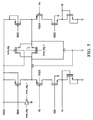
図7は、本開示の実施形態による、ADC100のより詳細な図である。図7に示されるように、種々の実施形態では、遅延ライン116、118は、随意に、トリミング対象遅延セル702、オーバーレンジ遅延セル704、およびデータ遅延セル706に分割されてもよい。いくつかの実施形態では、トリミング対象遅延セル702およびオーバーレンジ遅延セル704のうちの1つは、省略されてもよい。さらに、これらのセルのグループのうちの1つまたはそれを上回るものは、ADC100の所望の精度に従って、セルレンジに分割されてもよい。一実施形態では、データ遅延セル706は、所望の精度に従って、セルレンジに分割されてもよい。別の実施形態では、データ遅延セル706およびオーバーレンジ遅延セル704は、所望の精度に従って、セルレンジに分割されてもよい。
FIG. 7 is a more detailed view of the
例えば、遅延セルのいくつかは、マルチプレクサ712を伴うADC100のための5ビット精度をサポートするために必要とされるデータセルの数にグループ化されてもよい。別の実施例では、遅延セルのいくつかは、マルチプレクサ710を伴うADC100のための6ビット精度、またはマルチプレクサ708を伴うADC100のための7ビット精度をサポートするために必要とされるデータセルの数にグループ化されてもよい。各そのようなマルチプレクサは、マルチプレクサに続く遅延ライン内の遅延セルのための遅延動作を有効にし得る。したがって、遅延ラインの一部は、精密モードに従って、選択的にアクティブ化されてもよい。精度モードは、ADC100の所望のモード、ユーザまたはソフトウェア動作に従って、または過電圧状況または不足電圧状況に応答して、ADC100によって動的に設定されてもよい。5ビット精度の有効化は、done信号発生まで、全ての後続遅延セルを有効にし得る。同様に、6ビット精度の有効化は、done信号発生まで、全ての後続遅延セルを有効にし得る。5ビット精度遅延セルの有効化が、行われてもよい。同様に、7ビット精度の有効化は、done信号発生まで、全ての後続遅延セルを有効にし得る。5ビットおよび6ビット精度遅延セルの有効化も、行われてもよい。
For example, some of the delay cells may be grouped into the number of data cells required to support 5-bit precision for the
故に、異なる場合および異なる時間において、グループ704および706のいくつかの間に重複が存在し得る。オーバーレンジのために使用されないセルは、通常のデータのために使用され得る。同様に、データのために使用されないセルは、オーバーレンジのために使用され得る。さらに、随意のトリミング対象遅延セル702の構成が、グループ704または706の要素に適用されてもよい。ビットグループ708、710、712は、所与のそのようなビットグループ内の全体のグループに適用されるマルチプレクサを用いて遂行され得るが、個々のマルチプレクサは、その一部をトリミングするために適用されてもよい。
Therefore, there may be overlap between some of the
グループ702では、遅延セルのための個々のマルチプレクサは、伝搬ライン内の使用をトリミングまたは省略し得る。ある場合には、nbias遅延ライン内の遅延セルのためのマルチプレクサ動作は、pbias遅延ライン内の対応する遅延セルと異なり得る。故に、遅延ラインの長さは、pbiasまたはnbiasラインのうちの1つが他の遅延ラインと同じ数の遅延要素を通過しないように、オフセットを補償するように調節され得る。pbiasラインをトリミングするためのマルチプレクサは、bpのインデックス化されたコマンドを通して制御され得、nbiasラインをトリミングするためのマルチプレクサは、bnのインデックス化されたコマンドを通して制御され得る。遅延ラインのトリミングは、個別の電流値を較正し得る。
In
図8は、本開示の実施形態による、ADC100を組み込むように構成される、例示的システム、マイクロコントローラ800、または他のデバイスの例証である。ADC100は、DDL ADC812としてマイクロコントローラ800内に含まれてもよい。プロセッサ802、メモリ806、従来のADC810、およびPWM回路812もまた、含まれてもよい。これらは、好適なデータバス802を通して通信可能に結合されてもよい。
FIG. 8 is an illustration of an exemplary system,
DDL ADC812の動作は、プロセッサ802によるメモリ806内の命令の実行に応じて、マイクロコントローラ800の代わりに開始されてもよい。命令は、PWM812の種々の部分が電圧調整を行うためのものであってもよい。電圧調整の一部として、電圧比較が、DDL ADC812または従来のADC810によって行われてもよい。DDL ADC812からの結果に応じて、プロセッサ804は、是正措置を講じてもよい。例えば、PWM設定は、即時コンダクタ情報に基づいて調節され得る。
The operation of the
マイクロコントローラ800の残りに対するDDL ADC812の動作は、従来のADC810によって使用されるであろうような割込サービスルーチン(ISR)を使用する必要なく行われ得る。さらに、従来のADC810が使用されるときの場合に当てはまるであろうように、DDL ADC812を利用するために、直接メモリアクセス(DMA)の必要がなくてもよい。DDL ADC812の7つのインスタンスは、15nsコンパレータより小型であって、アナログコンパレータと同様に高速であり得る。
The operation of the
図9は、本開示の実施形態による、PWMを制御するためのデジタルコンパレータを特徴とするDDL ADCを伴うマイクロコントローラの例証である。 FIG. 9 is an example of a microcontroller with a DDL ADC comprising a digital comparator for controlling PWM according to an embodiment of the present disclosure.
他の用途では、純粋なアナログコンパレータが、適用を監視し、過電流条件または不足電流条件、または、過電圧条件または不足電圧条件条件を検出し、直接、PWM信号をオンまたはオフにし得る。しかしながら、そのようなアナログコンパレータは、単一出力に限定されず、高速であり得る。他の用途では、ADCは、デジタルコンパレータを組み込み、レンジ外動作を検出し、割込をプロセッサに発生させ、したがって、ソフトウェアは、PWMに調節を行うことができる。ADCは、複数のビットの出力をソフトウェアに提供することができるが、電源制御ループに対して低速である。 In other applications, a pure analog comparator may monitor the application, detect an overcurrent or undercurrent condition, or an overvoltage or undervoltage condition, and turn the PWM signal on or off directly. However, such analog comparators are not limited to a single output and can be fast. In other applications, the ADC incorporates a digital comparator to detect out-of-range operation and generate an interrupt in the processor, thus allowing the software to make adjustments to PWM. The ADC can provide the software with multiple bit outputs, but is slower than the power control loop.
ADC100の使用によって、マイクロコントローラは、ADC100の超高速を利用し得る。デジタルコンパレータおよび関連付けられたレジスタは、ADC100データ出力を監視し、データが比較基準を満たすとき、デジタル出力信号をアサートし得る。これらの出力信号は、PWM回路に接続され、PWM出力信号の即時制御(修正)を提供し得る。
By using the
ADC100のインスタンスは、その値を1つまたはそれを上回るPWMコントローラまたは回路に出力し得る。これらは、ADCバスを通して、直接、1つまたはそれを上回るデジタルコンパレータにルーティングされ得る。デジタルコンパレータは、個別のPWMコントローラまたは回路内に実装されてもよい、またはそこに通信可能に結合されてもよい。デジタルコンパレータは、ADC100信号が所与のデジタルコンパレータのために使用されるべきレジスタ値または他のインジケータを用いてプログラムされてもよい。したがって、デジタルコンパレータは、所与のADC100からのデータをサブスクライブする、または受け取るように指定され得る。さらに、デジタルコンパレータがADC100信号を比較すべき値は、レジスタ内に規定されてもよい。PWMコントローラは、差動電圧が、比較値レジスタ内に規定された閾値を上回るかどうかに基づいて、PWM信号を発行し得る。さらに、異なるレベルが、異なる比較値レジスタ内に規定されてもよい。PWMコントローラは、差動電圧に到達する閾値に基づいて、PWM信号を発行し得る。
An instance of
デジタルコンパレータはそれぞれ、2つの出力を有し得、第1の出力は、値が関連付けられたレジスタ内に記憶される値を上回ることを示し、第2の出力は、値が関連付けられたレジスタ内に記憶される値を下回るか等しいことを示す。他の実施形態によるコンパレータは、等しい、より大きい、より小さい、より大きいか等しい、より小さいか等しい等の異なる演算子の使用を示す、異なる出力を有し得る。コンパレータによって提供される出力信号は、PWMモジュールを直接制御するために使用され得る。本設計は、割込サービスルーチンを待機する必要がなく、DMA転送の必要もない。 Each digital comparator may have two outputs, the first output indicating that the value exceeds the value stored in the associated register, and the second output in the value associated register. Indicates that the value is less than or equal to the value stored in. Comparator according to other embodiments may have different outputs indicating the use of different operators such as equal, greater than, less than, greater than or equal to, less than or equal to. The output signal provided by the comparator can be used to directly control the PWM module. The present design does not need to wait for an interrupt service routine and does not require DMA transfer.
図10は、本開示の実施形態による、ADC100の別のより詳細な図である。図示されるのは、マルチプレクサ1006、1008である。マルチプレクサ1006、1008は、マルチプレクサ710、712と類似目的を果たし得る。マルチプレクサ710は、DDL端から50%点に設置されてもよい。マルチプレクサ712は、DDL端から25%点に設置されてもよい。示されない他のマルチプレクサも、例えば、DDL端から12.5%点に設置されてもよい。
FIG. 10 is another more detailed view of the
ADC100は、ブロック1002およびブロック1004等のデジタル論理ブロックを含み、データをラッチからロードしてもよい。デジタル論理ブロックのためのイネーブル信号は、マルチプレクサ有効化に結び付けられ得る。例えば、マルチプレクサ1006、1008が、完全分解能を有効にすることになると、ブロック1002および1004は、ラッチからの全てのデータのロードを可能にし得る。マルチプレクサ1006、1008が、半分解能を有効にすることになると、ブロック1002は、オフにされ得る一方、ブロック1004は、オンにされる。4分の1分解能等のための他の論理ブロックは、示されていない。そのようなブロックもまた、図7のマルチプレクサと協調して使用される。
The
端部により近い各マルチプレクサは、分解能を1ビット低減させるが、ADC100の遅延ラインの一部をシャットダウンするとき、変換の速度を2倍にする。データラッチとサーモメータ/バイナリコードコンバータとの間の論理ブロックのANDゲートは、異なる分解能選択のための適用可能な入力を選択する。そのような論理ブロックは、代わりに、遅延ラインとラッチとの間に実装され得る。
Each multiplexer closer to the end reduces the resolution by one bit, but doubles the conversion speed when shutting down part of the delay line of the
論理ブロックの使用によって、未使用遅延ラインタップ内の「1」は、データ結果が破損することを防止される。遅延ライン内に設置されたマルチプレクサはまた、リセット値を遅延における複数の点の中に挿入し、変換サイクルに続いてより高速のリセットをもたらすための機構を提供し得る。これは、次の変換が開始し得るとき、時間遅延を低減させ得る。
本開示の追加、変更、修正、または他の順列が、当業者の知識、技術、および理解に従って行われ得る。
By using the logical block, a "1" in the unused delay line tap prevents the data result from being corrupted. A multiplexer installed in the delay line may also provide a mechanism for inserting the reset value into multiple points in the delay, resulting in a faster reset following the conversion cycle. This can reduce the time delay when the next conversion can start.
Additions, changes, modifications, or other permutations of this disclosure may be made in accordance with the knowledge, skills, and understanding of those skilled in the art.
Claims (14)
入力回路と、
ソースからの入力差動電圧を差動電流に変換するように構成されるトランスコンダクタ入力段と、
2つのデジタル遅延ラインであって、前記2つのデジタル遅延ラインは、それぞれ、前記差動電流の第1の電流または第2の電流のどちらかを受信し、各デジタル遅延ラインは、
第1の回路であって、前記第1の回路は、遅延要素のセットを備え、各々、前記第1の電流または前記第2の電流によってバイアスされ、デジタル信号を遅延させるように構成され、前記入力回路は、前記2つのデジタル遅延ラインの第1のデジタル遅延ラインおよび第2のデジタル遅延ラインにデジタル信号をフィードし、前記第1のデジタル遅延ラインと前記第2のデジタル遅延ラインとの間の時間遅延が、前記第1の回路によって測定され、これにより、前記入力差動電圧のアナログ・デジタル変換を表すサーモメータコードを発生させる、第1の回路と、
前記第1の回路と直列に結合される構成可能な第2の回路であって、前記第2の回路は、遅延要素の別のセットを備え、各々、前記第1の電流または前記第2の電流によってバイアスされ、前記デジタル信号を遅延させるように構成される、第2の回路と
を備える、2つのデジタル遅延ラインと
を備え、
前記第2の回路は、前記2つのデジタル遅延ラインの前記第1のデジタル遅延ラインまたは前記第2のデジタル遅延ラインの長さを前記2つのデジタル遅延ラインのうちの他方のデジタル遅延ラインに対して個々に調節するように制御可能な関連付けられたマルチプレクサの有効化を通じて前記デジタル遅延ラインの各々において追加の遅延要素を追加するように構成される、アナログ・デジタルコンバータ。 Differential digital delay line analog-to-digital converter
With the input circuit
A transducer input stage configured to convert the input differential voltage from the source into a differential current,
Two digital delay lines, the two digital delay lines each receiving either the first current or the second current of the differential current, and each digital delay line is
A first circuit, the first circuit comprises a set of delay elements, each being biased by said first current or the second current, is configured to delay the digital signal, the The input circuit feeds a digital signal to the first digital delay line and the second digital delay line of the two digital delay lines, and between the first digital delay line and the second digital delay line. With the first circuit, the time delay is measured by the first circuit, thereby generating a thermometer code representing the analog-to-digital conversion of the input differential voltage .
A configurable second circuit coupled in series with the first circuit, wherein the second circuit comprises another set of delay elements, respectively, the first current or the second. With two digital delay lines, including a second circuit that is biased by current and configured to delay the digital signal.
Before Stories second circuit, with respect to the other digital delay line of said two of said first digital delay line or the second of the length of the digital delay line two digital delay lines of the digital delay line Add additional delay elements in each of the digital delay line through enabling controllable associated multiplexer to adjust individually Te urchin configured, analog-to-digital converter.
前記NANDゲートの出力と結合されるラッチと
をさらに備え、
前記ラッチは、前記デジタル遅延ラインのうちのより高速なものの完了に応じて、前記デジタル遅延ラインのうちのより低速のものからのデータを保存するように構成される、請求項1〜6のいずれかに記載のアナログ・デジタルコンバータ。 A plurality of NAND gates that receive output signals from each delay element of the first circuit, and
Further provided with a latch coupled to the output of the NAND gate
Any of claims 1-6 , wherein the latch is configured to store data from the slower of the digital delay lines upon completion of the faster of the digital delay lines. The analog-to-digital converter described in LINE.
前記NANDゲートの出力と結合されるラッチであって、前記ラッチは、前記デジタル遅延ラインのうちのより高速なものの完了に応じて、前記デジタル遅延ラインのうちのより低速のものからのデータを保存するように構成される、ラッチと
各遅延ラインの最後の遅延要素の出力と結合されるORゲートであって、前記ORゲートの出力は、前記ラッチを制御する信号を発生させるORゲートと
をさらに備え、前記アナログ・デジタルコンバータは、前記第3の回路のそれぞれの遅延要素から出力信号を受信する複数のさらなるNANDゲートをさらに備え、前記第3の回路の前記遅延要素の出力は、前記アナログ・デジタルコンバータへの入力が所定の入力レンジから外れている程度を示すオーバーフローデータを生成する、請求項9に記載のアナログ・デジタルコンバータ。 A plurality of NAND gates that receive output signals from each delay element of the first circuit, and
A latch coupled to the output of the NAND gate, which stores data from the slower of the digital delay lines upon completion of the faster of the digital delay lines. configured to, a OR gate coupled to the output of the last delay element of the latch and the delay line, the output of the OR gate, an OR gate Ru generates a signal for controlling the latch
Further wherein the analog to digital converter, the output of the delay element of the third further comprising a plurality of additional N the AND gate for receiving an output signal from the respective delay elements of the circuit of the third circuit, the input to the analog-to-digital converter to generate an overflow data indicating the extent to which out of a predetermined input range, the analog-to-digital converter according to claim 9.
ソースからの入力差動電圧を差動電流に変換することと、
第1のデジタル遅延ラインおよび第2のデジタル遅延ラインに前記差動電流をフィードすることであって、各デジタル遅延ラインは、第1の遅延要素のセットを備える第1の回路を備え、各々、前記差動電流のうちの第1の電流または第2の電流によってバイアスされ、デジタル信号を遅延させるように構成される、ことと、
前記第1の電流によって前記第1のデジタル遅延ラインの前記第1の回路の遅延要素をバイアスし、前記第2の電流によって前記第2のデジタル遅延ラインの前記第1の回路の遅延要素をバイアスすることと、
前記第1のデジタル遅延ラインおよび前記第2のデジタル遅延ラインにデジタル信号をフィードすることであって、前記第1のデジタル遅延ラインと前記第2のデジタル遅延ラインとの間の時間遅延が前記第1の回路によって測定され、それによって、前記入力差動電圧のアナログ・デジタル変換を表すサーモメータコードを発生させ、各デジタル遅延ラインは、前記第1の回路と直列に結合される構成可能な第2の回路をさらに備え、前記第2の回路は、遅延要素の別のセットを備え、各々、前記第1の電流または前記第2の電流によってバイアスされ、前記デジタル信号を遅延させるように構成される、ことと、
前記第1のデジタル遅延ラインまたは前記第2のデジタル遅延ラインの長さを他方のデジタル遅延ラインに対して調節するように、それぞれのマルチプレクサを通じて追加の遅延要素を前記第1のデジタル遅延ラインまたは前記第2のデジタル遅延ラインに個々に追加するように前記第2の回路を構成することと
を含む、方法。 A method for operating a differential digital delay line analog-to-digital converter, wherein the method is
Converting the input differential voltage from the source to a differential current,
Feeding the differential current to a first digital delay line and a second digital delay line, each digital delay line comprises a first circuit comprising a first set of delay elements, each of which comprises a first circuit. It said biased by a first current or a second current of the differential current, configured to delay the digital signals, and that,
The first current biases the delay element of the first circuit of the first digital delay line, and the second current biases the delay element of the first circuit of the second digital delay line. To do and
Feeding a digital signal to the first digital delay line and the second digital delay line, the time delay between the first digital delay line and the second digital delay line is the first. Measured by one circuit, thereby generating a thermometer code representing the analog-to-digital conversion of the input differential voltage , each digital delay line being configured to be coupled in series with the first circuit. The second circuit further comprises two circuits, each of which comprises another set of delay elements, each biased by the first current or the second current and configured to delay the digital signal. To and that
Additional delay elements are added through the respective multiplexers to the first digital delay line or said so that the length of the first digital delay line or the second digital delay line is adjusted relative to the other digital delay line. and a configuring the second circuit to add individually into a second digital delay line, the method.
Applications Claiming Priority (11)
| Application Number | Priority Date | Filing Date | Title |
|---|---|---|---|
| US201662321668P | 2016-04-12 | 2016-04-12 | |
| US201662321694P | 2016-04-12 | 2016-04-12 | |
| US201662321687P | 2016-04-12 | 2016-04-12 | |
| US201662321685P | 2016-04-12 | 2016-04-12 | |
| US62/321,685 | 2016-04-12 | ||
| US62/321,668 | 2016-04-12 | ||
| US62/321,687 | 2016-04-12 | ||
| US62/321,694 | 2016-04-12 | ||
| US15/484,949 | 2017-04-11 | ||
| US15/484,949 US9948317B2 (en) | 2016-04-12 | 2017-04-11 | Time-based delay line analog to digital converter |
| PCT/US2017/027191 WO2017180732A1 (en) | 2016-04-12 | 2017-04-12 | Time-based delay line analog to digital converter |
Publications (3)
| Publication Number | Publication Date |
|---|---|
| JP2019520716A JP2019520716A (en) | 2019-07-18 |
| JP2019520716A5 JP2019520716A5 (en) | 2020-04-30 |
| JP6929282B2 true JP6929282B2 (en) | 2021-09-01 |
Family
ID=59998462
Family Applications (4)
| Application Number | Title | Priority Date | Filing Date |
|---|---|---|---|
| JP2018523754A Pending JP2019514230A (en) | 2016-04-12 | 2017-04-12 | Time-based delay line analog to digital converter with variable resolution |
| JP2018523815A Active JP6934866B2 (en) | 2016-04-12 | 2017-04-12 | Digital Delay Line Microcontroller with analog-to-digital converter |
| JP2018523787A Active JP7036717B2 (en) | 2016-04-12 | 2017-04-12 | Digital Delay Line Microcontroller with analog-to-digital converter and digital comparator |
| JP2018523813A Active JP6929282B2 (en) | 2016-04-12 | 2017-04-12 | Time-based delay line analog-to-digital converter |
Family Applications Before (3)
| Application Number | Title | Priority Date | Filing Date |
|---|---|---|---|
| JP2018523754A Pending JP2019514230A (en) | 2016-04-12 | 2017-04-12 | Time-based delay line analog to digital converter with variable resolution |
| JP2018523815A Active JP6934866B2 (en) | 2016-04-12 | 2017-04-12 | Digital Delay Line Microcontroller with analog-to-digital converter |
| JP2018523787A Active JP7036717B2 (en) | 2016-04-12 | 2017-04-12 | Digital Delay Line Microcontroller with analog-to-digital converter and digital comparator |
Country Status (7)
| Country | Link |
|---|---|
| US (7) | US9948317B2 (en) |
| EP (4) | EP3443673A1 (en) |
| JP (4) | JP2019514230A (en) |
| KR (4) | KR20180127960A (en) |
| CN (4) | CN108432141B (en) |
| TW (4) | TW201810955A (en) |
| WO (4) | WO2017180778A1 (en) |
Families Citing this family (12)
| Publication number | Priority date | Publication date | Assignee | Title |
|---|---|---|---|---|
| US9948317B2 (en) * | 2016-04-12 | 2018-04-17 | Microchip Technology Incorporated | Time-based delay line analog to digital converter |
| FI128846B (en) * | 2017-03-20 | 2021-01-29 | Beamex Oy Ab | Automatic calibration of a measurement circuit |
| GB2567420B (en) * | 2017-10-02 | 2020-07-08 | Advanced Risc Mach Ltd | Adaptive voltage scaling methods and systems therefor |
| DE102017223466A1 (en) * | 2017-12-20 | 2019-06-27 | Dialog Semiconductor (Uk) Limited | ANALOG DIGITAL CONVERTER WITH SELF-TRACKING AND SELF-RANGING WINDOW |
| TWI696344B (en) | 2018-11-16 | 2020-06-11 | 財團法人工業技術研究院 | Linearity improving system and linearity improving method |
| TWI670939B (en) * | 2018-12-03 | 2019-09-01 | 新唐科技股份有限公司 | Delay line circuit with calibration function and calibration method thereof |
| CN109660302B (en) * | 2018-12-05 | 2021-08-03 | 中国人民解放军国防科技大学 | Radio frequency pulse width modulator based on digital delay line unit and modulation method |
| CN109639281A (en) * | 2018-12-18 | 2019-04-16 | 四川长虹电器股份有限公司 | A kind of voltage code circuit of the controllable gain for amplifier front-end |
| US10892746B2 (en) * | 2019-01-14 | 2021-01-12 | Texas Instruments Incorporated | Switch on-time controller with delay line modulator |
| CN115280690B (en) * | 2020-03-10 | 2024-03-19 | 哲库科技(上海)有限公司 | Methods, apparatus, systems, and media for delay line based transceiver calibration |
| IT202000013627A1 (en) | 2020-06-08 | 2021-12-08 | St Microelectronics Srl | A CONTROL CIRCUIT FOR AN ELECTRONIC CONVERTER, RELATED INTEGRATED CIRCUIT, ELECTRONIC CONVERTER AND PROCEDURE |
| CN114070316B (en) * | 2021-11-17 | 2023-04-14 | 苏州迅芯微电子有限公司 | Multi-phase clock generation circuit and analog-to-digital converter |
Family Cites Families (44)
| Publication number | Priority date | Publication date | Assignee | Title |
|---|---|---|---|---|
| US4471340A (en) * | 1981-06-02 | 1984-09-11 | The United States Of America As Represented By The Secretary Of The Navy | Analog to digital converter |
| DE3663860D1 (en) * | 1986-12-24 | 1989-07-13 | Hewlett Packard Gmbh | Method of and apparatus for adjusting the intensity profile of an ultrasound beam |
| US4998109A (en) * | 1989-12-13 | 1991-03-05 | Lechevalier Robert E | Analog to digital conversion device by charge integration using delay-line time measurement |
| US5140531A (en) * | 1990-08-01 | 1992-08-18 | General Electric Company | Analog neural nets supplied digital synapse signals on a bit-slice basis |
| US5412349A (en) * | 1992-03-31 | 1995-05-02 | Intel Corporation | PLL clock generator integrated with microprocessor |
| JP4229482B2 (en) * | 1997-10-24 | 2009-02-25 | 株式会社ルネサステクノロジ | Microcomputer with built-in flash memory |
| WO2000044098A1 (en) * | 1999-01-19 | 2000-07-27 | Steensgaard Madsen Jesper | Residue-compensating a / d converter |
| US6316987B1 (en) * | 1999-10-22 | 2001-11-13 | Velio Communications, Inc. | Low-power low-jitter variable delay timing circuit |
| US7595686B2 (en) * | 2001-11-09 | 2009-09-29 | The Regents Of The University Of Colorado | Digital controller for high-frequency switching power supplies |
| US7346638B2 (en) * | 2003-11-21 | 2008-03-18 | Board Of Regents, The University Of Texas System | Filtering, equalization, and power estimation for enabling higher speed signal transmission |
| US6977605B2 (en) * | 2003-11-26 | 2005-12-20 | Texas Instruments Incorporated | Dummy delay line based DLL and method for clocking in pipeline ADC |
| US20060038596A1 (en) * | 2004-08-18 | 2006-02-23 | Binan Wang | Delay locked loop circuitry and method for optimizing delay timing in mixed signal systems |
| CA2483378A1 (en) * | 2004-10-01 | 2006-04-01 | Aleksandar Prodic | A digital controller for dc-dc switching converters that allows operation at ultra-high constant switching frequencies |
| US7456620B2 (en) * | 2004-12-03 | 2008-11-25 | The Regents Of The University Of Colorado | Determining dead times in switched-mode DC-DC converters |
| US7315270B2 (en) * | 2005-03-04 | 2008-01-01 | The Regents Of The University Of Colorado | Differential delay-line analog-to-digital converter |
| US7902803B2 (en) * | 2005-03-04 | 2011-03-08 | The Regents Of The University Of Colorado | Digital current mode controller |
| WO2007054902A1 (en) * | 2005-11-11 | 2007-05-18 | Nxp B.V. | Integrating analog to digital converter |
| JP4702179B2 (en) * | 2006-05-22 | 2011-06-15 | 株式会社デンソー | A / D conversion circuit |
| US7414553B1 (en) | 2006-11-17 | 2008-08-19 | Zilog, Inc. | Microcontroller having in-situ autocalibrated integrating analog-to-digital converter (IADC) |
| US7525471B2 (en) | 2007-02-28 | 2009-04-28 | Exar Corporation | Wide-input windowed nonlinear analog-to-digital converter for high-frequency digitally controlled SMPS |
| US7652604B2 (en) | 2007-02-28 | 2010-01-26 | Exar Corporation | Programmable analog-to-digital converter for low-power DC-DC SMPS |
| DE102007026684B4 (en) * | 2007-06-08 | 2009-03-19 | Gesellschaft für Schwerionenforschung mbH | Time-amplitude converter component |
| KR100921815B1 (en) | 2007-06-18 | 2009-10-16 | 주식회사 애트랩 | Delay time measurement circuit and method |
| US8022849B2 (en) * | 2008-04-14 | 2011-09-20 | Qualcomm, Incorporated | Phase to digital converter in all digital phase locked loop |
| TWI392241B (en) * | 2009-02-18 | 2013-04-01 | Realtek Semiconductor Corp | Apparatus for processing echo signal and method thereof |
| KR101069671B1 (en) * | 2009-04-15 | 2011-10-04 | 주식회사 하이닉스반도체 | Circuit for changing frequency of a signal and frequency change method thereof |
| US7893861B2 (en) * | 2009-06-30 | 2011-02-22 | International Business Machines Corporation | Time-to-digital based analog-to-digital converter architecture |
| EP2330744A1 (en) * | 2009-11-30 | 2011-06-08 | Nxp B.V. | Analog to digital conversion circuit and method |
| JP2011160369A (en) * | 2010-02-04 | 2011-08-18 | Sony Corp | Electronic circuit, electronic apparatus, and digital signal processing method |
| US8283950B2 (en) * | 2010-08-11 | 2012-10-09 | Micron Technology, Inc. | Delay lines, amplifier systems, transconductance compensating systems and methods of compensating |
| US8289062B2 (en) * | 2010-09-16 | 2012-10-16 | Micron Technology, Inc. | Analog delay lines and adaptive biasing |
| US8487806B2 (en) * | 2010-11-26 | 2013-07-16 | Electronics And Telecommunications Research Institute | Voltage-time converters and time-domain voltage comparators including the same |
| US8542138B2 (en) * | 2011-01-28 | 2013-09-24 | The Regents Of The University Of California | Ring oscillator delta sigma ADC modulator with replica path nonlinearity calibration |
| KR101202742B1 (en) * | 2011-04-05 | 2012-11-19 | 연세대학교 산학협력단 | Time to digital converter and converting method |
| US8786338B2 (en) * | 2011-11-14 | 2014-07-22 | Texas Instruments Incorporated | Delay locked loop |
| CN102522994B (en) * | 2011-12-07 | 2015-01-14 | 清华大学 | Clock generation circuit used in analog-to-digital converter (ADC) with high speed and high precision |
| US9098072B1 (en) * | 2012-09-05 | 2015-08-04 | IQ-Analog Corporation | Traveling pulse wave quantizer |
| US8797079B2 (en) * | 2012-09-28 | 2014-08-05 | Intel Mobile Communications GmbH | Differential delay line, ring oscillator and mobile communication device |
| JP6085523B2 (en) * | 2013-05-30 | 2017-02-22 | ルネサスエレクトロニクス株式会社 | Semiconductor device and method of operating semiconductor device |
| KR101503732B1 (en) * | 2013-06-14 | 2015-03-20 | 연세대학교 산학협력단 | Time to digital converter |
| JP6071840B2 (en) * | 2013-10-25 | 2017-02-01 | 株式会社東芝 | A / D converter and semiconductor integrated circuit |
| US9312840B2 (en) * | 2014-02-28 | 2016-04-12 | Analog Devices Global | LC lattice delay line for high-speed ADC applications |
| JP2015167278A (en) * | 2014-03-03 | 2015-09-24 | 株式会社デンソー | Output switching method of a/d converter and a/d converter |
| US9948317B2 (en) * | 2016-04-12 | 2018-04-17 | Microchip Technology Incorporated | Time-based delay line analog to digital converter |
-
2017
- 2017-04-11 US US15/484,949 patent/US9948317B2/en active Active
- 2017-04-11 US US15/484,987 patent/US9906235B2/en active Active
- 2017-04-11 US US15/485,020 patent/US9923570B2/en active Active
- 2017-04-11 US US15/484,965 patent/US10090850B2/en active Active
- 2017-04-12 TW TW106112232A patent/TW201810955A/en unknown
- 2017-04-12 JP JP2018523754A patent/JP2019514230A/en active Pending
- 2017-04-12 CN CN201780005061.9A patent/CN108432141B/en active Active
- 2017-04-12 WO PCT/US2017/027262 patent/WO2017180778A1/en active Application Filing
- 2017-04-12 WO PCT/US2017/027243 patent/WO2017180765A1/en active Application Filing
- 2017-04-12 EP EP17733079.2A patent/EP3443673A1/en not_active Ceased
- 2017-04-12 JP JP2018523815A patent/JP6934866B2/en active Active
- 2017-04-12 EP EP17732613.9A patent/EP3443672A1/en not_active Ceased
- 2017-04-12 TW TW106112262A patent/TW201810957A/en unknown
- 2017-04-12 EP EP17719135.0A patent/EP3443671A1/en not_active Ceased
- 2017-04-12 TW TW106112233A patent/TW201810956A/en unknown
- 2017-04-12 TW TW106112234A patent/TW201803277A/en unknown
- 2017-04-12 KR KR1020187015388A patent/KR20180127960A/en unknown
- 2017-04-12 KR KR1020187015387A patent/KR20180127959A/en unknown
- 2017-04-12 CN CN201780005275.6A patent/CN108432144B/en active Active
- 2017-04-12 WO PCT/US2017/027191 patent/WO2017180732A1/en active Application Filing
- 2017-04-12 CN CN201780005126.XA patent/CN108432142B/en active Active
- 2017-04-12 JP JP2018523787A patent/JP7036717B2/en active Active
- 2017-04-12 KR KR1020187015385A patent/KR20180127957A/en unknown
- 2017-04-12 KR KR1020187015386A patent/KR20180127958A/en unknown
- 2017-04-12 JP JP2018523813A patent/JP6929282B2/en active Active
- 2017-04-12 WO PCT/US2017/027250 patent/WO2017180771A1/en active Application Filing
- 2017-04-12 EP EP17718779.6A patent/EP3443670A1/en not_active Ceased
- 2017-04-12 CN CN201780005127.4A patent/CN108432143B/en active Active
-
2018
- 2018-02-21 US US15/901,294 patent/US10355707B2/en active Active
- 2018-03-08 US US15/915,796 patent/US10122375B2/en active Active
- 2018-04-10 US US15/949,479 patent/US10171099B2/en active Active
Also Published As
Similar Documents
| Publication | Publication Date | Title |
|---|---|---|
| JP6929282B2 (en) | Time-based delay line analog-to-digital converter | |
| CN108702157B (en) | Delay line analog comparator based on time |
Legal Events
| Date | Code | Title | Description |
|---|---|---|---|
| A521 | Request for written amendment filed |
Free format text: JAPANESE INTERMEDIATE CODE: A523 Effective date: 20200318 |
|
| A621 | Written request for application examination |
Free format text: JAPANESE INTERMEDIATE CODE: A621 Effective date: 20200318 |
|
| A131 | Notification of reasons for refusal |
Free format text: JAPANESE INTERMEDIATE CODE: A131 Effective date: 20210315 |
|
| A521 | Request for written amendment filed |
Free format text: JAPANESE INTERMEDIATE CODE: A523 Effective date: 20210614 |
|
| TRDD | Decision of grant or rejection written | ||
| A01 | Written decision to grant a patent or to grant a registration (utility model) |
Free format text: JAPANESE INTERMEDIATE CODE: A01 Effective date: 20210713 |
|
| A61 | First payment of annual fees (during grant procedure) |
Free format text: JAPANESE INTERMEDIATE CODE: A61 Effective date: 20210810 |
|
| R150 | Certificate of patent or registration of utility model |
Ref document number: 6929282 Country of ref document: JP Free format text: JAPANESE INTERMEDIATE CODE: R150 |