JP6926246B2 - Dimensional reduced structured illumination microscope with nanowell patterned array - Google Patents
Dimensional reduced structured illumination microscope with nanowell patterned array Download PDFInfo
- Publication number
- JP6926246B2 JP6926246B2 JP2019571725A JP2019571725A JP6926246B2 JP 6926246 B2 JP6926246 B2 JP 6926246B2 JP 2019571725 A JP2019571725 A JP 2019571725A JP 2019571725 A JP2019571725 A JP 2019571725A JP 6926246 B2 JP6926246 B2 JP 6926246B2
- Authority
- JP
- Japan
- Prior art keywords
- biological sample
- optical
- diffraction grating
- image
- optical diffraction
- Prior art date
- Legal status (The legal status is an assumption and is not a legal conclusion. Google has not performed a legal analysis and makes no representation as to the accuracy of the status listed.)
- Active
Links
- 238000005286 illumination Methods 0.000 title description 29
- 230000003287 optical effect Effects 0.000 claims description 162
- 239000012472 biological sample Substances 0.000 claims description 85
- 238000003384 imaging method Methods 0.000 claims description 70
- 238000000034 method Methods 0.000 claims description 47
- 230000010363 phase shift Effects 0.000 claims description 26
- 230000010354 integration Effects 0.000 claims 1
- 239000000523 sample Substances 0.000 description 137
- 230000033001 locomotion Effects 0.000 description 30
- 230000003068 static effect Effects 0.000 description 18
- 238000012545 processing Methods 0.000 description 14
- 238000012163 sequencing technique Methods 0.000 description 12
- 239000000758 substrate Substances 0.000 description 12
- 238000004891 communication Methods 0.000 description 11
- 238000010586 diagram Methods 0.000 description 9
- 230000006870 function Effects 0.000 description 9
- 150000007523 nucleic acids Chemical class 0.000 description 9
- 239000011295 pitch Substances 0.000 description 9
- 230000005284 excitation Effects 0.000 description 7
- 108020004707 nucleic acids Proteins 0.000 description 7
- 102000039446 nucleic acids Human genes 0.000 description 7
- 230000001427 coherent effect Effects 0.000 description 6
- 238000004590 computer program Methods 0.000 description 6
- 230000004044 response Effects 0.000 description 6
- 238000004458 analytical method Methods 0.000 description 5
- 238000010223 real-time analysis Methods 0.000 description 5
- 238000005516 engineering process Methods 0.000 description 4
- 230000007246 mechanism Effects 0.000 description 4
- 238000012546 transfer Methods 0.000 description 4
- 238000003491 array Methods 0.000 description 3
- 239000012530 fluid Substances 0.000 description 3
- 230000006872 improvement Effects 0.000 description 3
- 239000007788 liquid Substances 0.000 description 3
- 238000012856 packing Methods 0.000 description 3
- 230000009467 reduction Effects 0.000 description 3
- 230000008901 benefit Effects 0.000 description 2
- 239000012620 biological material Substances 0.000 description 2
- 230000005540 biological transmission Effects 0.000 description 2
- 239000003153 chemical reaction reagent Substances 0.000 description 2
- OPTASPLRGRRNAP-UHFFFAOYSA-N cytosine Chemical compound NC=1C=CNC(=O)N=1 OPTASPLRGRRNAP-UHFFFAOYSA-N 0.000 description 2
- 238000000799 fluorescence microscopy Methods 0.000 description 2
- UYTPUPDQBNUYGX-UHFFFAOYSA-N guanine Chemical compound O=C1NC(N)=NC2=C1N=CN2 UYTPUPDQBNUYGX-UHFFFAOYSA-N 0.000 description 2
- 239000000463 material Substances 0.000 description 2
- 239000011159 matrix material Substances 0.000 description 2
- 239000002773 nucleotide Substances 0.000 description 2
- 125000003729 nucleotide group Chemical group 0.000 description 2
- 239000013307 optical fiber Substances 0.000 description 2
- 238000005192 partition Methods 0.000 description 2
- 230000003954 pattern orientation Effects 0.000 description 2
- 230000008569 process Effects 0.000 description 2
- 230000005855 radiation Effects 0.000 description 2
- 238000007493 shaping process Methods 0.000 description 2
- 239000007787 solid Substances 0.000 description 2
- 238000001228 spectrum Methods 0.000 description 2
- RWQNBRDOKXIBIV-UHFFFAOYSA-N thymine Chemical compound CC1=CNC(=O)NC1=O RWQNBRDOKXIBIV-UHFFFAOYSA-N 0.000 description 2
- 229930024421 Adenine Natural products 0.000 description 1
- GFFGJBXGBJISGV-UHFFFAOYSA-N Adenine Chemical compound NC1=NC=NC2=C1N=CN2 GFFGJBXGBJISGV-UHFFFAOYSA-N 0.000 description 1
- 241000473391 Archosargus rhomboidalis Species 0.000 description 1
- 238000012935 Averaging Methods 0.000 description 1
- 238000001712 DNA sequencing Methods 0.000 description 1
- 229920002307 Dextran Polymers 0.000 description 1
- 102000004190 Enzymes Human genes 0.000 description 1
- 108090000790 Enzymes Proteins 0.000 description 1
- 108091034117 Oligonucleotide Proteins 0.000 description 1
- 239000004743 Polypropylene Substances 0.000 description 1
- 239000004793 Polystyrene Substances 0.000 description 1
- XUIMIQQOPSSXEZ-UHFFFAOYSA-N Silicon Chemical compound [Si] XUIMIQQOPSSXEZ-UHFFFAOYSA-N 0.000 description 1
- JLCPHMBAVCMARE-UHFFFAOYSA-N [3-[[3-[[3-[[3-[[3-[[3-[[3-[[3-[[3-[[3-[[3-[[5-(2-amino-6-oxo-1H-purin-9-yl)-3-[[3-[[3-[[3-[[3-[[3-[[5-(2-amino-6-oxo-1H-purin-9-yl)-3-[[5-(2-amino-6-oxo-1H-purin-9-yl)-3-hydroxyoxolan-2-yl]methoxy-hydroxyphosphoryl]oxyoxolan-2-yl]methoxy-hydroxyphosphoryl]oxy-5-(5-methyl-2,4-dioxopyrimidin-1-yl)oxolan-2-yl]methoxy-hydroxyphosphoryl]oxy-5-(6-aminopurin-9-yl)oxolan-2-yl]methoxy-hydroxyphosphoryl]oxy-5-(6-aminopurin-9-yl)oxolan-2-yl]methoxy-hydroxyphosphoryl]oxy-5-(6-aminopurin-9-yl)oxolan-2-yl]methoxy-hydroxyphosphoryl]oxy-5-(6-aminopurin-9-yl)oxolan-2-yl]methoxy-hydroxyphosphoryl]oxyoxolan-2-yl]methoxy-hydroxyphosphoryl]oxy-5-(5-methyl-2,4-dioxopyrimidin-1-yl)oxolan-2-yl]methoxy-hydroxyphosphoryl]oxy-5-(4-amino-2-oxopyrimidin-1-yl)oxolan-2-yl]methoxy-hydroxyphosphoryl]oxy-5-(5-methyl-2,4-dioxopyrimidin-1-yl)oxolan-2-yl]methoxy-hydroxyphosphoryl]oxy-5-(5-methyl-2,4-dioxopyrimidin-1-yl)oxolan-2-yl]methoxy-hydroxyphosphoryl]oxy-5-(6-aminopurin-9-yl)oxolan-2-yl]methoxy-hydroxyphosphoryl]oxy-5-(6-aminopurin-9-yl)oxolan-2-yl]methoxy-hydroxyphosphoryl]oxy-5-(4-amino-2-oxopyrimidin-1-yl)oxolan-2-yl]methoxy-hydroxyphosphoryl]oxy-5-(4-amino-2-oxopyrimidin-1-yl)oxolan-2-yl]methoxy-hydroxyphosphoryl]oxy-5-(4-amino-2-oxopyrimidin-1-yl)oxolan-2-yl]methoxy-hydroxyphosphoryl]oxy-5-(6-aminopurin-9-yl)oxolan-2-yl]methoxy-hydroxyphosphoryl]oxy-5-(4-amino-2-oxopyrimidin-1-yl)oxolan-2-yl]methyl [5-(6-aminopurin-9-yl)-2-(hydroxymethyl)oxolan-3-yl] hydrogen phosphate Polymers Cc1cn(C2CC(OP(O)(=O)OCC3OC(CC3OP(O)(=O)OCC3OC(CC3O)n3cnc4c3nc(N)[nH]c4=O)n3cnc4c3nc(N)[nH]c4=O)C(COP(O)(=O)OC3CC(OC3COP(O)(=O)OC3CC(OC3COP(O)(=O)OC3CC(OC3COP(O)(=O)OC3CC(OC3COP(O)(=O)OC3CC(OC3COP(O)(=O)OC3CC(OC3COP(O)(=O)OC3CC(OC3COP(O)(=O)OC3CC(OC3COP(O)(=O)OC3CC(OC3COP(O)(=O)OC3CC(OC3COP(O)(=O)OC3CC(OC3COP(O)(=O)OC3CC(OC3COP(O)(=O)OC3CC(OC3COP(O)(=O)OC3CC(OC3COP(O)(=O)OC3CC(OC3COP(O)(=O)OC3CC(OC3COP(O)(=O)OC3CC(OC3CO)n3cnc4c(N)ncnc34)n3ccc(N)nc3=O)n3cnc4c(N)ncnc34)n3ccc(N)nc3=O)n3ccc(N)nc3=O)n3ccc(N)nc3=O)n3cnc4c(N)ncnc34)n3cnc4c(N)ncnc34)n3cc(C)c(=O)[nH]c3=O)n3cc(C)c(=O)[nH]c3=O)n3ccc(N)nc3=O)n3cc(C)c(=O)[nH]c3=O)n3cnc4c3nc(N)[nH]c4=O)n3cnc4c(N)ncnc34)n3cnc4c(N)ncnc34)n3cnc4c(N)ncnc34)n3cnc4c(N)ncnc34)O2)c(=O)[nH]c1=O JLCPHMBAVCMARE-UHFFFAOYSA-N 0.000 description 1
- 229960000643 adenine Drugs 0.000 description 1
- 230000000712 assembly Effects 0.000 description 1
- 238000000429 assembly Methods 0.000 description 1
- 239000011324 bead Substances 0.000 description 1
- 230000015572 biosynthetic process Effects 0.000 description 1
- 239000000872 buffer Substances 0.000 description 1
- 230000015556 catabolic process Effects 0.000 description 1
- 230000001413 cellular effect Effects 0.000 description 1
- 238000003776 cleavage reaction Methods 0.000 description 1
- 239000003086 colorant Substances 0.000 description 1
- 230000000295 complement effect Effects 0.000 description 1
- 150000001875 compounds Chemical class 0.000 description 1
- 239000006059 cover glass Substances 0.000 description 1
- 229940104302 cytosine Drugs 0.000 description 1
- 238000006731 degradation reaction Methods 0.000 description 1
- 238000001514 detection method Methods 0.000 description 1
- 201000010099 disease Diseases 0.000 description 1
- 208000037265 diseases, disorders, signs and symptoms Diseases 0.000 description 1
- 230000000694 effects Effects 0.000 description 1
- 239000007850 fluorescent dye Substances 0.000 description 1
- 239000000499 gel Substances 0.000 description 1
- 239000011521 glass Substances 0.000 description 1
- PCHJSUWPFVWCPO-UHFFFAOYSA-N gold Chemical compound [Au] PCHJSUWPFVWCPO-UHFFFAOYSA-N 0.000 description 1
- 239000010931 gold Substances 0.000 description 1
- 229910052737 gold Inorganic materials 0.000 description 1
- 230000003993 interaction Effects 0.000 description 1
- 230000001788 irregular Effects 0.000 description 1
- 239000004816 latex Substances 0.000 description 1
- 229920000126 latex Polymers 0.000 description 1
- 238000004519 manufacturing process Methods 0.000 description 1
- 238000000386 microscopy Methods 0.000 description 1
- 238000011022 operating instruction Methods 0.000 description 1
- 238000011017 operating method Methods 0.000 description 1
- 230000000737 periodic effect Effects 0.000 description 1
- 239000004033 plastic Substances 0.000 description 1
- 229920003023 plastic Polymers 0.000 description 1
- 229920000747 poly(lactic acid) Polymers 0.000 description 1
- 229920002401 polyacrylamide Polymers 0.000 description 1
- 229920001690 polydopamine Polymers 0.000 description 1
- -1 polypropylene Polymers 0.000 description 1
- 229920001155 polypropylene Polymers 0.000 description 1
- 229920002223 polystyrene Polymers 0.000 description 1
- 102000004169 proteins and genes Human genes 0.000 description 1
- 108090000623 proteins and genes Proteins 0.000 description 1
- 238000011160 research Methods 0.000 description 1
- 230000007017 scission Effects 0.000 description 1
- 229910052710 silicon Inorganic materials 0.000 description 1
- 239000010703 silicon Substances 0.000 description 1
- 238000010561 standard procedure Methods 0.000 description 1
- 238000012360 testing method Methods 0.000 description 1
- 229940113082 thymine Drugs 0.000 description 1
- 238000013519 translation Methods 0.000 description 1
- 238000013024 troubleshooting Methods 0.000 description 1
- 235000012431 wafers Nutrition 0.000 description 1
Images


Classifications
-
- B—PERFORMING OPERATIONS; TRANSPORTING
- B01—PHYSICAL OR CHEMICAL PROCESSES OR APPARATUS IN GENERAL
- B01L—CHEMICAL OR PHYSICAL LABORATORY APPARATUS FOR GENERAL USE
- B01L3/00—Containers or dishes for laboratory use, e.g. laboratory glassware; Droppers
- B01L3/50—Containers for the purpose of retaining a material to be analysed, e.g. test tubes
- B01L3/502—Containers for the purpose of retaining a material to be analysed, e.g. test tubes with fluid transport, e.g. in multi-compartment structures
-
- G—PHYSICS
- G01—MEASURING; TESTING
- G01N—INVESTIGATING OR ANALYSING MATERIALS BY DETERMINING THEIR CHEMICAL OR PHYSICAL PROPERTIES
- G01N21/00—Investigating or analysing materials by the use of optical means, i.e. using sub-millimetre waves, infrared, visible or ultraviolet light
- G01N21/62—Systems in which the material investigated is excited whereby it emits light or causes a change in wavelength of the incident light
- G01N21/63—Systems in which the material investigated is excited whereby it emits light or causes a change in wavelength of the incident light optically excited
- G01N21/64—Fluorescence; Phosphorescence
- G01N21/645—Specially adapted constructive features of fluorimeters
- G01N21/6452—Individual samples arranged in a regular 2D-array, e.g. multiwell plates
-
- B—PERFORMING OPERATIONS; TRANSPORTING
- B01—PHYSICAL OR CHEMICAL PROCESSES OR APPARATUS IN GENERAL
- B01L—CHEMICAL OR PHYSICAL LABORATORY APPARATUS FOR GENERAL USE
- B01L3/00—Containers or dishes for laboratory use, e.g. laboratory glassware; Droppers
- B01L3/50—Containers for the purpose of retaining a material to be analysed, e.g. test tubes
- B01L3/508—Containers for the purpose of retaining a material to be analysed, e.g. test tubes rigid containers not provided for above
- B01L3/5085—Containers for the purpose of retaining a material to be analysed, e.g. test tubes rigid containers not provided for above for multiple samples, e.g. microtitration plates
- B01L3/50851—Containers for the purpose of retaining a material to be analysed, e.g. test tubes rigid containers not provided for above for multiple samples, e.g. microtitration plates specially adapted for heating or cooling samples
-
- B—PERFORMING OPERATIONS; TRANSPORTING
- B01—PHYSICAL OR CHEMICAL PROCESSES OR APPARATUS IN GENERAL
- B01L—CHEMICAL OR PHYSICAL LABORATORY APPARATUS FOR GENERAL USE
- B01L3/00—Containers or dishes for laboratory use, e.g. laboratory glassware; Droppers
- B01L3/50—Containers for the purpose of retaining a material to be analysed, e.g. test tubes
- B01L3/508—Containers for the purpose of retaining a material to be analysed, e.g. test tubes rigid containers not provided for above
- B01L3/5085—Containers for the purpose of retaining a material to be analysed, e.g. test tubes rigid containers not provided for above for multiple samples, e.g. microtitration plates
- B01L3/50853—Containers for the purpose of retaining a material to be analysed, e.g. test tubes rigid containers not provided for above for multiple samples, e.g. microtitration plates with covers or lids
-
- B—PERFORMING OPERATIONS; TRANSPORTING
- B82—NANOTECHNOLOGY
- B82Y—SPECIFIC USES OR APPLICATIONS OF NANOSTRUCTURES; MEASUREMENT OR ANALYSIS OF NANOSTRUCTURES; MANUFACTURE OR TREATMENT OF NANOSTRUCTURES
- B82Y15/00—Nanotechnology for interacting, sensing or actuating, e.g. quantum dots as markers in protein assays or molecular motors
-
- G—PHYSICS
- G01—MEASURING; TESTING
- G01N—INVESTIGATING OR ANALYSING MATERIALS BY DETERMINING THEIR CHEMICAL OR PHYSICAL PROPERTIES
- G01N21/00—Investigating or analysing materials by the use of optical means, i.e. using sub-millimetre waves, infrared, visible or ultraviolet light
- G01N21/01—Arrangements or apparatus for facilitating the optical investigation
- G01N21/03—Cuvette constructions
- G01N21/05—Flow-through cuvettes
-
- G—PHYSICS
- G01—MEASURING; TESTING
- G01N—INVESTIGATING OR ANALYSING MATERIALS BY DETERMINING THEIR CHEMICAL OR PHYSICAL PROPERTIES
- G01N21/00—Investigating or analysing materials by the use of optical means, i.e. using sub-millimetre waves, infrared, visible or ultraviolet light
- G01N21/62—Systems in which the material investigated is excited whereby it emits light or causes a change in wavelength of the incident light
- G01N21/63—Systems in which the material investigated is excited whereby it emits light or causes a change in wavelength of the incident light optically excited
- G01N21/64—Fluorescence; Phosphorescence
- G01N21/645—Specially adapted constructive features of fluorimeters
- G01N21/6456—Spatial resolved fluorescence measurements; Imaging
- G01N21/6458—Fluorescence microscopy
-
- G—PHYSICS
- G02—OPTICS
- G02B—OPTICAL ELEMENTS, SYSTEMS OR APPARATUS
- G02B21/00—Microscopes
-
- G—PHYSICS
- G02—OPTICS
- G02B—OPTICAL ELEMENTS, SYSTEMS OR APPARATUS
- G02B21/00—Microscopes
- G02B21/06—Means for illuminating specimens
-
- G—PHYSICS
- G02—OPTICS
- G02B—OPTICAL ELEMENTS, SYSTEMS OR APPARATUS
- G02B21/00—Microscopes
- G02B21/16—Microscopes adapted for ultraviolet illumination ; Fluorescence microscopes
-
- G—PHYSICS
- G02—OPTICS
- G02B—OPTICAL ELEMENTS, SYSTEMS OR APPARATUS
- G02B21/00—Microscopes
- G02B21/36—Microscopes arranged for photographic purposes or projection purposes or digital imaging or video purposes including associated control and data processing arrangements
- G02B21/365—Control or image processing arrangements for digital or video microscopes
-
- G—PHYSICS
- G02—OPTICS
- G02B—OPTICAL ELEMENTS, SYSTEMS OR APPARATUS
- G02B27/00—Optical systems or apparatus not provided for by any of the groups G02B1/00 - G02B26/00, G02B30/00
- G02B27/42—Diffraction optics, i.e. systems including a diffractive element being designed for providing a diffractive effect
- G02B27/4233—Diffraction optics, i.e. systems including a diffractive element being designed for providing a diffractive effect having a diffractive element [DOE] contributing to a non-imaging application
- G02B27/425—Diffraction optics, i.e. systems including a diffractive element being designed for providing a diffractive effect having a diffractive element [DOE] contributing to a non-imaging application in illumination systems
-
- G—PHYSICS
- G02—OPTICS
- G02B—OPTICAL ELEMENTS, SYSTEMS OR APPARATUS
- G02B27/00—Optical systems or apparatus not provided for by any of the groups G02B1/00 - G02B26/00, G02B30/00
- G02B27/58—Optics for apodization or superresolution; Optical synthetic aperture systems
-
- G—PHYSICS
- G06—COMPUTING; CALCULATING OR COUNTING
- G06V—IMAGE OR VIDEO RECOGNITION OR UNDERSTANDING
- G06V10/00—Arrangements for image or video recognition or understanding
- G06V10/10—Image acquisition
-
- B—PERFORMING OPERATIONS; TRANSPORTING
- B01—PHYSICAL OR CHEMICAL PROCESSES OR APPARATUS IN GENERAL
- B01L—CHEMICAL OR PHYSICAL LABORATORY APPARATUS FOR GENERAL USE
- B01L2300/00—Additional constructional details
- B01L2300/06—Auxiliary integrated devices, integrated components
- B01L2300/0627—Sensor or part of a sensor is integrated
- B01L2300/0654—Lenses; Optical fibres
-
- B—PERFORMING OPERATIONS; TRANSPORTING
- B01—PHYSICAL OR CHEMICAL PROCESSES OR APPARATUS IN GENERAL
- B01L—CHEMICAL OR PHYSICAL LABORATORY APPARATUS FOR GENERAL USE
- B01L2300/00—Additional constructional details
- B01L2300/06—Auxiliary integrated devices, integrated components
- B01L2300/0627—Sensor or part of a sensor is integrated
- B01L2300/0663—Whole sensors
-
- B—PERFORMING OPERATIONS; TRANSPORTING
- B01—PHYSICAL OR CHEMICAL PROCESSES OR APPARATUS IN GENERAL
- B01L—CHEMICAL OR PHYSICAL LABORATORY APPARATUS FOR GENERAL USE
- B01L2300/00—Additional constructional details
- B01L2300/08—Geometry, shape and general structure
- B01L2300/0893—Geometry, shape and general structure having a very large number of wells, microfabricated wells
-
- B—PERFORMING OPERATIONS; TRANSPORTING
- B01—PHYSICAL OR CHEMICAL PROCESSES OR APPARATUS IN GENERAL
- B01L—CHEMICAL OR PHYSICAL LABORATORY APPARATUS FOR GENERAL USE
- B01L2300/00—Additional constructional details
- B01L2300/08—Geometry, shape and general structure
- B01L2300/0896—Nanoscaled
-
- G—PHYSICS
- G01—MEASURING; TESTING
- G01N—INVESTIGATING OR ANALYSING MATERIALS BY DETERMINING THEIR CHEMICAL OR PHYSICAL PROPERTIES
- G01N21/00—Investigating or analysing materials by the use of optical means, i.e. using sub-millimetre waves, infrared, visible or ultraviolet light
- G01N21/62—Systems in which the material investigated is excited whereby it emits light or causes a change in wavelength of the incident light
- G01N21/63—Systems in which the material investigated is excited whereby it emits light or causes a change in wavelength of the incident light optically excited
- G01N21/64—Fluorescence; Phosphorescence
- G01N2021/6417—Spectrofluorimetric devices
- G01N2021/6419—Excitation at two or more wavelengths
-
- G—PHYSICS
- G01—MEASURING; TESTING
- G01N—INVESTIGATING OR ANALYSING MATERIALS BY DETERMINING THEIR CHEMICAL OR PHYSICAL PROPERTIES
- G01N21/00—Investigating or analysing materials by the use of optical means, i.e. using sub-millimetre waves, infrared, visible or ultraviolet light
- G01N21/62—Systems in which the material investigated is excited whereby it emits light or causes a change in wavelength of the incident light
- G01N21/63—Systems in which the material investigated is excited whereby it emits light or causes a change in wavelength of the incident light optically excited
- G01N21/64—Fluorescence; Phosphorescence
- G01N2021/6417—Spectrofluorimetric devices
- G01N2021/6421—Measuring at two or more wavelengths
-
- G—PHYSICS
- G01—MEASURING; TESTING
- G01N—INVESTIGATING OR ANALYSING MATERIALS BY DETERMINING THEIR CHEMICAL OR PHYSICAL PROPERTIES
- G01N21/00—Investigating or analysing materials by the use of optical means, i.e. using sub-millimetre waves, infrared, visible or ultraviolet light
- G01N21/62—Systems in which the material investigated is excited whereby it emits light or causes a change in wavelength of the incident light
- G01N21/63—Systems in which the material investigated is excited whereby it emits light or causes a change in wavelength of the incident light optically excited
- G01N21/64—Fluorescence; Phosphorescence
- G01N21/645—Specially adapted constructive features of fluorimeters
- G01N2021/6482—Sample cells, cuvettes
-
- G—PHYSICS
- G01—MEASURING; TESTING
- G01N—INVESTIGATING OR ANALYSING MATERIALS BY DETERMINING THEIR CHEMICAL OR PHYSICAL PROPERTIES
- G01N21/00—Investigating or analysing materials by the use of optical means, i.e. using sub-millimetre waves, infrared, visible or ultraviolet light
- G01N21/62—Systems in which the material investigated is excited whereby it emits light or causes a change in wavelength of the incident light
- G01N21/63—Systems in which the material investigated is excited whereby it emits light or causes a change in wavelength of the incident light optically excited
- G01N21/64—Fluorescence; Phosphorescence
- G01N21/6408—Fluorescence; Phosphorescence with measurement of decay time, time resolved fluorescence
Landscapes
- Chemical & Material Sciences (AREA)
- Health & Medical Sciences (AREA)
- Physics & Mathematics (AREA)
- Analytical Chemistry (AREA)
- General Physics & Mathematics (AREA)
- General Health & Medical Sciences (AREA)
- Engineering & Computer Science (AREA)
- Life Sciences & Earth Sciences (AREA)
- Optics & Photonics (AREA)
- Immunology (AREA)
- Pathology (AREA)
- Biochemistry (AREA)
- Chemical Kinetics & Catalysis (AREA)
- Hematology (AREA)
- Clinical Laboratory Science (AREA)
- Nuclear Medicine, Radiotherapy & Molecular Imaging (AREA)
- Multimedia (AREA)
- Theoretical Computer Science (AREA)
- Nanotechnology (AREA)
- Molecular Biology (AREA)
- Crystallography & Structural Chemistry (AREA)
- Computer Vision & Pattern Recognition (AREA)
- Investigating, Analyzing Materials By Fluorescence Or Luminescence (AREA)
- Microscoopes, Condenser (AREA)
- Apparatus Associated With Microorganisms And Enzymes (AREA)
Description
本出願は、2018年1月24日に出願された発明の名称が「ナノウェルのパターン化アレイを有する次元低下構造化照明顕微鏡」である米国仮特許出願第62/621,564号、および2018年3月20日に出願された「ナノウェルのパターン化アレイを有する次元低下構造化照明顕微鏡」という名称のオランダ特許出願第N2020622号の優先権を主張する。上記各出願の全内容を参照により本明細書に援用するものとする。 This application is filed on January 24, 2018, and the title of the invention is "Dimensional Degradation Structured Illumination Microscope with Nanowell Patterned Array", US Provisional Patent Application No. 62 / 621,564, and March 2018. Claims the priority of Dutch Patent Application No. N2020622 entitled "Degraded Structured Illumination Microscope with Nanowell Patterned Arrays" filed on the 20th. The entire contents of each of the above applications shall be incorporated herein by reference.
生物学の研究における多くの最近の進歩は、核酸の分析および配列決定のための改善された方法から利益を得てきた。例えば、ヒトゲノムプロジェクトでは、期待されるヒトゲノムの全塩基配列が決定されており、疾病の治療から基礎科学の進歩に至るまでの分野でさらなる発見につながるであろう。平面アレイの形態またはビーズ上のいずれかでの、増幅されていないまたは増幅された単一分子の大規模な並行分析に基づく、多数の新しいDNA配列決定技術が、最近報告されている。 Many recent advances in biological research have benefited from improved methods for nucleic acid analysis and sequencing. For example, the Human Genome Project has determined the expected entire base sequence of the human genome, which will lead to further discoveries in fields ranging from disease treatment to advances in basic science. A number of new DNA sequencing techniques based on large-scale parallel analysis of unamplified or amplified single molecules, either in the form of planar arrays or on beads, have recently been reported.
このような新しい配列決定技術において核酸の配列を分析するために使用される方法はしばしば、蛍光ヌクレオチドまたはオリゴヌクレオチドの検出に基づく。構造化照明顕微鏡法(SIM)は空間的に構造化された(すなわち、パターン化された)光を使用して、顕微鏡の横方向分解能を2倍以上増大させるために試料を撮像することができる、1つのそのような配列決定技術を記載する。試料の撮像中、試料の画像は種々のパターン位相(例えば、0°、120°、および240°)で取得することができ、その手続はパターン配向を光軸を中心に(例えば、60°および120°だけ)回転させることによって繰り返される。捕捉された画像(例えば、9つの画像、各パターン位相における各配向角度に関する1つの画像)は、拡張された空間周波数帯域幅を有する単一の画像に組み立てることができる。単一の画像は顕微鏡によって通常解像可能であるよりも高い分解能を有する画像を生成するために、実空間に再変換されてもよい。 The methods used to analyze nucleic acid sequences in such new sequencing techniques are often based on the detection of fluorescent or oligonucleotides. Structured Illumination Microscopy (SIM) can use spatially structured (ie, patterned) light to image a sample to more than double the lateral resolution of the microscope. , One such sequencing technique is described. During imaging of the sample, the image of the sample can be obtained in various pattern phases (eg 0 °, 120 °, and 240 °) and the procedure is to align the pattern around the optical axis (eg 60 ° and eg 60 ° and). Repeated by rotating (only 120 °). The captured images (eg, nine images, one image for each orientation angle in each pattern phase) can be assembled into a single image with extended spatial frequency bandwidth. A single image may be reconverted into real space to produce an image with higher resolution than is normally resolvable by a microscope.
SIMシステムの典型的な実施態様では、直線偏光ビームが正弦波干渉縞模様として結像試料上に投影され得る2つ以上の別個の次数にビームを回折する、光学回折格子を通って導かれる。これらの実施形態では、投影された光回折格子パターンの配向が光軸を中心にして光回折格子を回転させることによって制御され、一方、パターンの位相は光学回折格子を軸をわたって横方向に移動させることによって調整される。このようなシステムでは、光学回折格子が平行移動ステージ上に取り付けられ、次いで、回転ステージ上に取り付けられる。加えて、このようなシステムは、直線偏光子を使用して、光源によって放射された光を、回折格子で受光される前に偏光させる。 In a typical embodiment of a SIM system, a linearly polarized beam is guided through an optical grating that diffracts the beam into two or more distinct orders that can be projected onto the imaging sample as a sinusoidal interference fringe pattern. In these embodiments, the orientation of the projected optical grating pattern is controlled by rotating the grating around the optical axis, while the phase of the pattern is lateral across the optical grating. Adjusted by moving. In such a system, the optical diffraction grating is mounted on the translation stage and then on the rotating stage. In addition, such a system uses a linear polarizer to polarize the light emitted by the light source before it is received by the grating.
図1Aは、試料100及び試料100上に投影された光学回折格子パターン102の一例を示す。試料100は分解不可能なより高い空間周波数を含み得るが、試料100上に既知のより低い空間周波数を有する光回折格子パターン102を重ね合わせると、モアレ縞が生じる。このことは、分解不可能なより高い空間周波数を、顕微鏡によって分解可能なより低い空間周波数に効果的に移動させる。上述したように、光学回折格子パターン102の試料100に対して異なる方位/角度および位相を有する、試料100の画像を捕捉することにより、より高い分解能を有する画像を生成するために実空間に再変換される単一の画像に組み合わせることが可能な画像が得られる。
FIG. 1A shows an example of the
本明細書に開示されるシステムおよび方法の例は、特にパターン化されたフローセルを通してSIMを使用して蛍光試料を分解するために必要とされる画像および次元の数を低減するための技術、ならびに線走査技術と共に使用することができるSIMの実施を達成するために蛍光試料に対する光ビームの移動を活用するための技術を対象とする。 Examples of systems and methods disclosed herein include techniques for reducing the number of images and dimensions required to decompose fluorescent samples using SIM, especially through patterned flow cells. The subject is a technique for utilizing the movement of a light beam with respect to a fluorescent sample to achieve a SIM implementation that can be used with line scanning techniques.
一実施形態によれば、生物学試料を撮像する方法は、生物学試料上に光学パターンを投影し、生物学試料上でオーバーレイされる光学パターンの第1画像を捕捉する投影ステップを含む。さらに、本方法は、投影される光学パターンを生物学試料に対して位相シフトし、位相シフトされるとともに生物学試料上でオーバーレイされる光学パターンの少なくとも第2画像を捕捉する位相シフトステップを含むことができる。またさらに、本方法は、捕捉される第1画像及び捕捉される少なくとも第2画像に基づいて、生物学試料を表す高解像度画像を再構成する再構成ステップを含むことができる。 According to one embodiment, the method of imaging a biological sample comprises a projection step of projecting an optical pattern onto the biological sample and capturing a first image of the optical pattern overlaid on the biological sample. Further, the method includes a phase shift step of phase shifting the projected optical pattern with respect to the biological sample and capturing at least a second image of the optical pattern that is phase shifted and overlaid on the biological sample. be able to. Furthermore, the method can include a reconstruction step of reconstructing a high resolution image representing a biological sample based on the captured first image and at least the captured second image.
いくつかの例では、生物学試料は、複数の細長いナノウェルを含み非対称にパターン化されるフローセルに含まれる。いくつかの例では、複数の細長いナノウェルのそれぞれは、楕円形状に成形され又は矩形状に成形される。いくつかの例では、複数の細長いナノウェルのそれぞれは、非対称にパターン化されるフローセルの第1軸に沿って生物学試料を表す情報を解像する解像度が向上するように配向される。いくつかの例では、複数の細長いナノウェルのそれぞれは、非対称にパターン化されるフローセルの第2軸に沿って生物学試料を表す情報を解像する解像度は向上しないように配向される。 In some examples, the biological sample is contained in an asymmetrically patterned flow cell containing multiple elongated nanowells. In some examples, each of the plurality of elongated nanowells is formed into an elliptical shape or a rectangular shape. In some examples, each of the elongated nanowells is oriented along the first axis of the asymmetrically patterned flow cell to improve the resolution of the information representing the biological sample. In some examples, each of the elongated nanowells is oriented along the second axis of the asymmetrically patterned flow cell so as not to improve the resolution of the information representing the biological sample.
いくつかの実施形態では、第1画像及び少なくとも第2画像の捕捉は、ライン走査撮像を実行することを含む。本方法は、光を、第1位相及び第1角度配向の光学回折格子に向け、光学回折格子を通すことをさらに含むことができ、生物学試料上に投影される光学パターンは、光学回折格子を通る光が生成する光学回折格子パターンであり、位相シフトステップは、光学回折格子を位相シフトすることを含む。光学回折格子を位相シフトすることは、光学回折格子を第1角度配向に沿って位相シフトすることを含むことができる。光学回折格子を位相シフトすることは、ライン走査撮像の方向と直交して起こり得る。 In some embodiments, capturing the first image and at least the second image involves performing a line scan imaging. The method can further include directing light to an optical diffraction grating of first phase and first angular orientation and passing through the optical diffraction grating, and the optical pattern projected onto the biological sample is an optical diffraction grating. It is an optical diffraction grating pattern generated by light passing through the optical diffraction grating, and the phase shift step includes a phase shift of the optical diffraction grating. Phase-shifting the optical diffraction grating can include phase-shifting the optical diffraction grating along the first angular orientation. Phase shifting the optical diffraction grating can occur orthogonal to the direction of the line scan imaging.
いくつかの例では、本方法は、高解像度画像を再構成する前に、光学回折格子の第3位相シフトを実行し、光学回折格子パターンを生物学試料上に投影し、位相シフトされるとともに生物学試料上でオーバーレイされる光学回折格子パターンの少なくとも第3画像を捕捉することをさらに含むことができる。 In some examples, the method performs a third phase shift of the optical grating before reconstructing the high resolution image, projects the optical grating pattern onto the biological sample, and is phase shifted as well. Capturing at least a third image of the optical grating pattern overlaid on the biological sample can further be included.
いくつかの例では、生物学試料を撮像する方法は、光を、第1位相及び第1角度配向の光学回折格子に向け、前記光学回折格子を通す配向ステップと、光学回折格子を通る光が生物学試料上に生成する光学回折格子パターンを投影し、生物学試料上でオーバーレイされる光学回折格子パターンの第1画像を捕捉する投影ステップと、を含む。本方法はさらに、光学回折格子を位相シフトし、光学回折格子パターンを生物学試料上に投影し、位相シフトされるとともに生物学試料上でオーバーレイされる光学回折格子パターンの少なくとも第2画像を捕捉する第2画像捕捉ステップを含むことができる。さらにまた、本方法は、光学回折格子を第2角度配向に再配向させ、光学回折格子パターンを生物学試料上に投影し、生物学試料上でオーバーレイされる光学回折格子パターンの第3画像を捕捉する第3画像捕捉ステップを含むことができる。そのうえ、本方法は、光学回折格子を位相シフトし、光学回折格子パターンを生物学試料上に投影し、位相シフトされるとともに生物学試料上でオーバーレイされる光学回折格子パターンの少なくとも第4画像を捕捉する第4画像捕捉ステップを含むことができる。さらに、本方法は、捕捉される、第1画像、少なくとも第2画像、第3画像及び少なくとも第4画像に基づいて、生物学試料を表す高解像度画像を再構成する再構成ステップを含むことができる。 In some examples, the method of imaging a biological sample directs light to an optical grating with first phase and first angular orientation, with an alignment step through the grating and light passing through the grating. It comprises a projection step of projecting an optical grating pattern generated on a biological sample and capturing a first image of the optical grating pattern overlaid on the biological sample. The method further phase shifts the optical grating pattern, projects the optical diffraction grating pattern onto the biological sample, and captures at least a second image of the optical diffraction grating pattern that is phase shifted and overlaid on the biological sample. The second image acquisition step to be performed can be included. Furthermore, in this method, the optical diffraction grating is reoriented to the second angular orientation, the optical diffraction grating pattern is projected onto the biological sample, and the third image of the optical diffraction grating pattern superimposed on the biological sample is obtained. A third image capture step to capture can be included. Moreover, the method phase shifts the optical diffraction grating, projects the optical diffraction grating pattern onto the biological sample, and produces at least a fourth image of the optical diffraction grating pattern that is phase shifted and overlaid on the biological sample. A fourth image capture step to capture can be included. In addition, the method may include a reconstruction step of reconstructing a high resolution image representing a biological sample based on the captured first, at least second, third and at least fourth images. can.
いくつかの例では、生物学試料が、複数のナノウェルを含む正方形状アレイパターン化フローセルに包含される。 In some examples, the biological sample is contained in a square array patterned flow cell containing multiple nanowells.
いくつかの例では、システムは、光線を放射するレーザ源と、放射される光線が通過すると光学回折格子パターンを生成するように適合される光学回折格子と、カメラアセンブリと、を備えることができる。カメラアセンブリは、生物学試料上でオーバーレイされる光学回折格子パターンの複数の画像を捕捉するように適合することができ、複数の画像は、光学回折格子の生物学試料に対する3つの位相を反映する。システムは、複数の画像の組み合わせに基づいて、生物学試料を表す高解像度画像を再構成するように適合されるプロセッサをさらに備えることができる。 In some examples, the system can include a laser source that emits a ray, an optical grating that is adapted to produce an optical grating pattern when the emitted ray passes through, and a camera assembly. .. The camera assembly can be adapted to capture multiple images of the optical grating pattern overlaid on the biological sample, and the multiple images reflect the three phases of the optical grating with respect to the biological sample. .. The system can further include a processor adapted to reconstruct a high resolution image representing a biological sample based on a combination of multiple images.
いくつかの例では、生物学試料は、非対称アレイに配向される複数のナノウェルを含むフローセルに配置される。いくつかの例では、複数のナノウェルのそれぞれは、楕円形状に成形され、又は矩形状に成形される。いくつかの例では、複数のナノウェルのそれぞれは、フローセルの第1軸に沿って生物学試料を表す情報を解像する解像度が向上するように配向される。いくつかの例では、複数のナノウェルのそれぞれは、フローセルの第2軸に沿って生物学試料を表す情報を解像する解像度は向上しないように配向される。 In some examples, the biological sample is placed in a flow cell containing multiple nanowells oriented in an asymmetric array. In some examples, each of the plurality of nanowells is formed into an elliptical shape or a rectangular shape. In some examples, each of the nanowells is oriented along the first axis of the flow cell to improve the resolution of the information representing the biological sample. In some examples, each of the nanowells is oriented along the second axis of the flow cell so as not to improve the resolution of the information representing the biological sample.
いくつかの例では、カメラアセンブリは、時間遅延積分ライン走査カメラアセンブリを備える。いくつかの例では、生物学試料はフローセルに包含され、フローセルの様々な部分が、オーバーレイされ、光学回折格子の3つの位相を同時に表す。 In some examples, the camera assembly comprises a time delay integrating line scanning camera assembly. In some examples, the biological sample is contained in a flow cell, where various parts of the flow cell are overlaid to simultaneously represent the three phases of the optical grating.
いくつかの例では、システムの光学回折格子は、3つの位相ステップ素子を備え、3つの位相ステップ素子のそれぞれは、放射される光線が位相ステップ素子を通過すると光学回折格子パターンを生成するように適合され、カメラアセンブリは、3つの位相ステップ素子のそれぞれが生成するとともに生物学試料上でオーバーレイされる光学回折格子パターンの画像を捕捉するように適合される。いくつかの例では、カメラアセンブリは、3つのイメージセンサを備え、3つのイメージセンサのそれぞれは、位相ステップ素子のそれぞれが生成する光学回折格子パターンの画像を捕捉するように適合される。 In some examples, the optical grating of the system comprises three phase step elements so that each of the three phase step elements produces an optical grating pattern as the emitted light passes through the phase step elements. Adapted, the camera assembly is adapted to capture an image of the optical grating pattern that each of the three phase step elements produces and overlays on the biological sample. In some examples, the camera assembly comprises three image sensors, each of which is adapted to capture an image of the optical grating pattern produced by each of the phase step elements.
他の実施形態によれば、システムは、光線を放射するレーザ源と、放射される光線が通過すると光学回折格子パターンを生成するように適合される光学回折格子と、生物学試料上でオーバーレイされる光学回折格子パターンの複数の画像を捕捉するように適合されるカメラアセンブリと、を備えることができ、複数の画像は、光学回折格子の生物学試料に対する3つの位相と、光学回折格子の生物学試料に対する2つの角度配向とを反映する。システムは、複数の画像の組み合わせに基づいて、生物学試料を表す高解像度画像を再構成するように適合されるプロセッサをさらに備えることができる。 According to another embodiment, the system is overlaid on a biological sample with a laser source that emits light and an optical grating that is adapted to produce an optical grating pattern when the emitted light passes through. Can include a camera assembly adapted to capture multiple images of the optical grating pattern, the plurality of images being the three phases of the optical grating with respect to the biological sample and the organisms of the optical grating. It reflects the two angular orientations with respect to the optics. The system can further include a processor adapted to reconstruct a high resolution image representing a biological sample based on a combination of multiple images.
いくつかの例では、生物学試料が、正方形状のアレイに配向される複数のナノウェルを含むフローセルに配置される。 In some examples, the biological sample is placed in a flow cell containing multiple nanowells oriented in a square array.
いくつかの例では、複数のナノウェルのそれぞれは、フローセルの第1軸及び第2軸に沿って生物学試料を表す情報を解像する解像度が向上するように配向される。 In some examples, each of the nanowells is oriented along the first and second axes of the flow cell to improve the resolution of the information representing the biological sample.
前述の概念と、以下でより詳細に論じられる追加の概念とのすべての組合せが、(そのような概念が相互に矛盾しないという条件で)本明細書で開示される本発明の主題の一部であると考えられることを理解されたい。特に、本開示の末尾にある特許請求の範囲の主題のすべての組み合わせは、本明細書に開示される本発明の主題の一部であると考えられる。 All combinations of the above concepts with the additional concepts discussed in more detail below are part of the subject matter of the invention disclosed herein (provided that such concepts are consistent with each other). Please understand that it is considered to be. In particular, all combinations of claims at the end of this disclosure are considered to be part of the subject matter of the invention disclosed herein.
開示された技術の他の構成及び態様は、例として、開示された技術の実施形態による構成を示す添付の図面と併せて、以下の詳細な説明から明らかになるであろう。この概要は、特許請求の範囲及び均等物によって定められる、本明細書に記載される任意の発明の範囲を限定することを意図しない。 Other configurations and embodiments of the disclosed technology will become apparent from the following detailed description, as an example, along with the accompanying drawings showing the configuration according to embodiments of the disclosed technology. This summary is not intended to limit the scope of any invention described herein, as defined by the claims and equivalents.
本開示は、1つ以上の様々な実装形態に従って、以下の図面を参照して詳細に説明される。図面は、説明のみを目的として提供され、典型的または例示的実施形態を単に示す。 The present disclosure is described in detail with reference to the following drawings according to one or more different implementations. The drawings are provided for illustration purposes only and merely show typical or exemplary embodiments.
図面は、網羅的ではなく、開示された厳密な形態に本開示を限定するものではない。 The drawings are not exhaustive and do not limit this disclosure to the exact form disclosed.
本明細書において回折格子によって放たれる回折光を指すように使用される場合、「次」または「次数」という用語は、強め合う干渉のための隣接する回折格子のスリットからの光の経路長差を表す波長の整数を意味することを意図している。「0次」または「0次最大」という用語は、回折がない回折格子によって放出された中央の明るい縞を指すことを意図している。「1次」という用語は、0次縞のいずれかの側に放たれる2つの明るい縞を指すことを意図しており、経路長差は±1波長である。 When used herein to refer to diffracted light emitted by a grating, the terms "next" or "order" are the path lengths of light from adjacent grating slits for intensifying interference. It is intended to mean an integer of wavelengths that represents the difference. The terms "0th order" or "0th order maximum" are intended to refer to the central bright fringes emitted by a diffraction grating without diffraction. The term "first order" is intended to refer to two bright fringes emitted on either side of the 0th order fringe, with a path length difference of ± 1 wavelength.
試料を参照するために本明細書で使用されるときに、用語「スポット」または「特徴」は、相対位置に従って他の点または領域から区別され得るパターン内の点または領域を意味することが意図される。個々のスポットは、特定の型の1つ以上の分子を含み得る。例えば、スポットは、特定の同一配列を有する単一の標的核酸分子を含み得るか、またはスポットは同じ配列(および/またはその相補的配列)を有するいくつかの核酸分子を含み得る。 As used herein to refer to a sample, the term "spot" or "feature" is intended to mean a point or region within a pattern that can be distinguished from other points or regions according to their relative position. Will be done. Each spot may contain one or more molecules of a particular type. For example, the spot may contain a single target nucleic acid molecule having a particular identical sequence, or the spot may contain several nucleic acid molecules having the same sequence (and / or complementary sequences thereof).
本明細書で使用される「タイル」という用語は一般に、試料の同じ領域の1つ以上の画像を指し、1つ以上の画像のそれぞれは、それぞれの色チャネルを表す。タイルは、1つの撮像サイクルの撮像データセットの撮像データサブセットを形成することができる。 As used herein, the term "tile" generally refers to one or more images of the same area of a sample, each of which represents its own color channel. The tiles can form an imaging data subset of the imaging dataset for one imaging cycle.
本明細書で使用される用語「x-y平面」は、デカルト座標系における直線軸xおよびyによって定義される2次元領域を意味することを意図している。検出器および検出器によって観察される物体に関して使用される場合、領域は、検出器と検出される物体との間の観察方向に直交するものとしてさらに特定され得る。本明細書でラインスキャナに言及するために使用される場合、用語「y方向」は走査の方向を意味する。 As used herein, the term "x-y plane" is intended to mean a two-dimensional region defined by the linear axes x and y in a Cartesian coordinate system. When used with respect to the detector and the object observed by the detector, the region may be further identified as orthogonal to the observation direction between the detector and the object to be detected. As used herein to refer to a line scanner, the term "y direction" means the direction of scanning.
本明細書で使用されるとき、用語「z座標」は、x-y平面に直交する軸に沿った点、線、または領域の位置を特定する情報を意味することが意図される。特定の実施形態では、z軸が検出器によって観察される物体の領域に直交する。例えば、光学系に対するフォーカスの方向は、z軸に沿って指定されてもよい。 As used herein, the term "z coordinate" is intended to mean information that locates a point, line, or region along an axis that is orthogonal to the x-y plane. In certain embodiments, the z-axis is orthogonal to the region of the object observed by the detector. For example, the direction of focus with respect to the optical system may be specified along the z-axis.
本明細書で使用される用語「ライン走査」は物体のx-y平面内の2次元断面を検出することを意味し、その断面は矩形または楕円形であり、断面と物体との間に相対的移動を生じさせることを意図している。例えば、蛍光イメージングの場合、矩形または楕円形の形状を有する物体の面積は(他の面積を除いて)特異的に励起することができ、および/または当該面積からの放射はスキャンの所与の時点で(他の面積を除いて)特異的に獲得し得る。 As used herein, the term "line scanning" means detecting a two-dimensional cross section of an object in the xy plane, which is rectangular or elliptical and moves relative to the cross section and the object. Is intended to cause. For example, in the case of fluorescence imaging, the area of an object having a rectangular or oval shape can be specifically excited (except for other areas), and / or radiation from that area is given in the scan. It can be acquired specifically at a point in time (except for other areas).
本明細書で開示される実施形態は、正方形または非対称パターンを有するように構成されたフローセルを対象とする。SIMは顕微鏡の横方向分解能を2倍以上増大させるために、試料を撮像するために空間的に構造化された(すなわち、パターン化された)光に依存することを思い出されたい。また、伝統的に、複数のパターン位相および複数の配向/角度における試料の画像が、横方向分解能の所望の増加を達成するために使用されることを思い出してほしい。 The embodiments disclosed herein are directed to flow cells configured to have a square or asymmetric pattern. Recall that SIM relies on spatially structured (ie, patterned) light to image a sample in order to more than double the lateral resolution of the microscope. Also, recall that traditionally, images of samples in multiple pattern phases and multiple orientations / angles are used to achieve the desired increase in lateral resolution.
図1Bは、概して、1つの例において、顕微鏡対物レンズ(その回折パターンに類似している)によって生成される逆格子空間の観察可能領域と、それが対物レンズが透過できる最も高い空間周波数(2NA / λ(グラフ120))によってエッジでどのように制限されるかを示す。図示のように、中心スポットは0次成分を表す。平行な線のパターンを表す0次および1次の回折成分が、グラフ122に示されている。パターン間隔が解像度の限界にある場合、一次スポットは観測可能なフィールドの端(k0の境界上)で発生する。周波数混合のため、観察可能領域は、空間周波数の正像(中心円)に加えて、元のフィールドのエッジを中心とする2つの新しいオフセット周波数画像(グラフ124)も含む。これらのオフセット画像は、従来の顕微鏡を用いては観測できないより高い空間周波数を含んでいる。グラフ126によって示されるように、120°の方位の3つの位相から作られた画像のセットは最終的には処理後に、広視野蛍光顕微鏡で観察され得るような空間解像度の2倍を含む実画像を生じる。
Figure 1B generally shows, in one example, the observable region of the reciprocal lattice space produced by the microscope objective (similar to its diffraction pattern) and the highest spatial frequency (2NA) through which the objective can pass. / λ (Graph 120)) shows how it is constrained by the edge. As shown, the central spot represents the 0th order component. The 0th and 1st order diffraction components representing the pattern of parallel lines are shown in
しかしながら、(例えば、六角形パターンではなく)正方形または非対称パターンを有するようにフローセルを構成することによって、基板を分解するために必要とされる分解能向上が異方性となるので、必要な画像がより少数となり、より制限されたSIM角度セットを使用することを通して異方性光学伝達関数(OTF)を構築することは、基板を十分な程度まで分解するために十分となる。すなわち、ナノウェルの正方形または非対称パターンを有するフローセルは、より狭いピッチ(すなわち、すぐ隣接するナノウェル間の距離)を有し、解像度の増加を伴うフローセルの1つ以上の軸が、解像度が増加されるべき1つ以上の軸と整列されることを可能にする。正方形のパターン化されたフローセルの1つの例では、解像度の増加が2つの軸に関してのみ必要である。したがって、6つの画像のみが必要とされる(3つの位相にわたる2つの角度の各々における画像)。非対称にパターン化されたフローセルの場合、試料の3つの画像のみが、増大した解像度(3つの位相にわたる1つの角度の画像)を達成するために必要である。 However, by configuring the flow cell to have a square or asymmetric pattern (eg, rather than a hexagonal pattern), the resolution improvement required to disassemble the substrate becomes anisotropic, so that the required image is Building an anisotropic optical transfer function (OTF) through the use of a smaller and more restricted set of SIM angles is sufficient to decompose the substrate to a sufficient degree. That is, a flow cell with a square or asymmetric pattern of nanowells has a narrower pitch (ie, the distance between immediately adjacent nanowells), and one or more axes of the flow cell with increased resolution will have increased resolution. Allows alignment with one or more axes to be. In one example of a square patterned flow cell, an increase in resolution is needed only for the two axes. Therefore, only 6 images are needed (images at each of the two angles over the three phases). For asymmetrically patterned flow cells, only three images of the sample are needed to achieve increased resolution (an image of one angle over three phases).
試料を所望の程度に分解するのに必要な角度の数を減らすことによって、試料の撮像を完了するのに必要な画像の数が減る。例えば、4色素化学の文脈において、システムは、塩基呼び出しのための4つの画像を生成するために36の画像を取得する必要があり得る(以下に説明される)。キャプチャされた画像を格納またはキャッシュするために必要な記憶装置(例えば、ディスク)空間の量も減少させることができる。さらに、画像を単一の画像に組み立て、次いでその単一の画像を所望の解像度を有する画像に再変換/再構成するのに必要な処理能力および/または計算能力も低減することができる。 By reducing the number of angles required to decompose the sample to the desired degree, the number of images required to complete the imaging of the sample is reduced. For example, in the context of tetrachromic chemistry, the system may need to acquire 36 images to generate 4 images for base calls (explained below). The amount of storage (eg, disk) space required to store or cache captured images can also be reduced. In addition, the processing and / or computational power required to assemble the image into a single image and then reconvert / reconstruct the single image into an image with the desired resolution can be reduced.
さらに、SIMの従来の実施は、試料を撮像するためにライン走査技術を利用するシーケンシングシステムと互換性がない。ライン走査は(例えばフローセルのような、物体全体の静止画像を捕捉する画素の2次元アレイを有するカメラまたはセンサとは対照的に)連続画像を構築するために、線毎にフローセルを撮像する画素の線を使用することに言及することができる。シーケンスシステムに適した1つの特定のタイプの線走査は、時間遅延積分(TDI)ライン走査である。 Moreover, conventional practices of SIM are incompatible with sequencing systems that utilize line scanning techniques to image the sample. Line scanning is a pixel that captures a flow cell line by line to build a continuous image (as opposed to a camera or sensor that has a two-dimensional array of pixels that capture a still image of the entire object, such as a flow cell). Can be mentioned to use the line of. One particular type of line scan suitable for sequence systems is the Time Delay Integral (TDI) line scan.
マルチアングルSIMの実施形態では、角度/位相画像の組み合わせの各々を取得するために、固定された視野が必要とされる。しかしながら、非対称にパターン化されたフローセルが試料基板として使用される本明細書に開示される実施形態の場合のように、単一の角度のみに関して画像が撮影される場合、TDIライン走査を使用して、3つのSIMパターン位相をカバーする試料の画像を取り込むことができる。すなわち、SIMパターンを非対称にパターン化されたフローセルに対して移動させて、1つの軸のみに沿って分解能を増大させてフローセル内の試料を分解するのに必要な3つの位相を生成することができる。 In the embodiment of the multi-angle SIM, a fixed field of view is required to acquire each of the angle / phase image combinations. However, TDI line scanning is used when images are taken with respect to only a single angle, as in the embodiments disclosed herein where an asymmetrically patterned flow cell is used as the sample substrate. It is possible to capture an image of a sample that covers the three SIM pattern phases. That is, the SIM pattern can be moved relative to the asymmetrically patterned flow cell to increase the resolution along only one axis and generate the three phases needed to decompose the sample in the flow cell. can.
いくつかの実施形態では、TDIライン走査は、フローセル(「スワス」と呼ばれる)に沿って画像を取り込むためにTDIライン走査カメラまたはセンサを使用することによって試料を撮像するためにSIM技術と併せて使用することができる。すなわち、TDIライン走査は、第1の位相でSIMパターンでパターン化されたフローセル上で実行することができる。SIMパターンは第2の位相にシフトすることができ、TDIライン走査を繰り返すことができる。SIMパターンは第3のフレーズにシフトされ、TDIライン走査は再び繰り返されることができる。このようにして、各パターン位相における試料の画像が捕捉される。 In some embodiments, TDI line scanning is combined with SIM technology to image a sample by using a TDI line scanning camera or sensor to capture an image along a flow cell (called a "swath"). Can be used. That is, the TDI line scan can be performed on a flow cell patterned with a SIM pattern in the first phase. The SIM pattern can be shifted to the second phase and the TDI line scan can be repeated. The SIM pattern is shifted to the third phrase and the TDI line scan can be repeated again. In this way, the image of the sample at each pattern phase is captured.
あるいは、フローセルの異なる部分を、SIMパターンの異なる位相でパターン化することができる。例えば、フローセルの第1の部分ではSIMパターンがフローセルの第1の位置に位置することができ、フローセルの第2の部分ではSIMパターンは第2の位置にシフトすることができ、フローセルの第3の部分ではSIMパターンが第3の位置にシフトすることができる。従って、カメラ又はセンサがスワスを捕捉するときに、3つのSIMパターン位相の各々にわたる試料の画像が単一のTDIライン走査で捕捉される。 Alternatively, different parts of the flow cell can be patterned with different phases of the SIM pattern. For example, in the first part of the flow cell the SIM pattern can be located in the first position of the flow cell, in the second part of the flow cell the SIM pattern can be shifted to the second position and in the third part of the flow cell. In the part of, the SIM pattern can be shifted to the third position. Thus, when a camera or sensor captures swath, an image of the sample across each of the three SIM pattern phases is captured in a single TDI line scan.
TDIライン走査のいくつかの実施態様は、投影された縞模様の3つの位相が1回の走査で指定され得る3チップTDIイメージャを用いて実施され得る。このような実装は、回折格子の各部分が特定の位相に対応する3部分回折格子を用いて実装することができる。例えば、3素子回折格子を、各素子が位相ステップ状に形成されるとともに、同一の基板上に形成してもよい。この実装により、走査方向に沿った移動とは別に、格子又は試料の移動は必要とされない。 Some embodiments of the TDI line scan can be performed using a 3-chip TDI imager in which the three phases of the projected striped pattern can be specified in a single scan. Such an implementation can be implemented using a three-part diffraction grating in which each portion of the grating corresponds to a specific phase. For example, a three-element diffraction grating may be formed on the same substrate while each element is formed in a phase step pattern. With this implementation, movement of the grid or sample is not required apart from movement along the scanning direction.
さらに他の実施態様では、試料/フローセルに対してSIMパターンをシフトさせる代わりに、SIMパターンが静止したままで試料/フローセルを移動させる。試料はフローセル内に配置/設置され、その結果、フローセルを構成するナノウェルに従って試料がパターン化されることが理解される。上述したように、TDIライン走査を実施する場合、試料/フローセルは既に移動している。したがって、試料/フローセルのこの移動を活用して、SIMパターンをシフトする必要を回避することができる。すなわち、静止SIMパターン(適切な配向が与えられる)に対する試料/フローセルの移動は、試料を分解するために必要とされる必要な位相を生成する。 In yet another embodiment, instead of shifting the SIM pattern relative to the sample / flow cell, the sample / flow cell is moved while the SIM pattern remains stationary. It is understood that the sample is placed / placed within the flow cell and as a result the sample is patterned according to the nanowells that make up the flow cell. As mentioned above, when performing a TDI line scan, the sample / flow cell has already moved. Therefore, this movement of the sample / flow cell can be leveraged to avoid the need to shift the SIM pattern. That is, the movement of the sample / flow cell with respect to the static SIM pattern (given the proper orientation) produces the required phase required to decompose the sample.
幾つかの実施形態では、格子及びウェルパターンはわずかな角度オフセットで構成することができ、3つの薄い照明領域が比較的遠く離れて試料上に投影される。各照明ライン内ではウェルが、主に格子と同位相のままであり得るが、照明領域間の距離は第2の照明領域によって、それらが位相シフトのために位相がラムダ/3ずれるのに十分であり得る。このような実施形態における照明ライン間の間隔は互いに隣接する3つの画像センサ(例えば、3つのTDIスキャナチップ)を有することをより容易にすることができる。この例示的なシナリオを図12に示す。 In some embodiments, the grid and well pattern can be configured with a slight angular offset, and three thin illuminated areas are projected onto the sample relatively far apart. Within each illumination line, the wells can remain predominantly in phase with the grid, but the distance between the illumination regions is sufficient for them to be lambda / 3 out of phase due to the phase shift due to the second illumination region. Can be. The spacing between the illumination lines in such an embodiment can make it easier to have three image sensors (eg, three TDI scanner chips) adjacent to each other. An exemplary scenario is shown in Figure 12.
本明細書で開示されるシステムおよび方法の様々な実装を詳細に説明する前に、本明細書で開示される技術を実装することができる例示的な環境を説明することが有用である。そのような例示的環境の1つは、図2に示される、空間的に構造化された光で試料を照らす構造化照明撮像システム200の環境である。例えば、システム200は、生物学的サンプルを撮像するために空間的に構造化された励起光を利用する構造化照明蛍光顕微鏡システムであってもよい。
Before elaborating on the various implementations of the systems and methods disclosed herein, it is useful to describe an exemplary environment in which the techniques disclosed herein can be implemented. One such exemplary environment is the environment of the structured
図2の例では、発光体250がコリメーションレンズ251によってコリメートされた光線を出力するように構成されている。コリメートされた光は、光構造化光学アセンブリ255によって構造化(パターン化)され、ダイクロイックミラー260によって、対物レンズ242を介して、段階270上に配置された試料容器210の試料上に向けられる。蛍光試料の場合、試料は構造化された励起光に応答して蛍光を発し、得られた光は、対物レンズ242によって収集され、カメラシステム240のイメージセンサに導かれて、蛍光を検出する。
In the example of FIG. 2, the
以下にさらに記載される様々な実装における光構造化光学アセンブリ255は、1つ以上の光学回折格子を含み、試料容器210の試料上に投射される回折光(例えば縞)の正弦パターンを生成する。回折格子は、一次元又は二次元の透過格子、反射格子又は位相格子であってよい。特定の実装を参照して以下でさらに説明するように、システム200では、回折格子は必ずしも回転ステージを含まない。幾つかの実施形態では、回折格子が撮像システムの動作中に固定されてもよい(例えば、回転されない、または直線的に移動されない)。例えば、以下に更に記載される特定の実施形態において、回折格子は互いに実質的に又は正確に/完全に垂直に配向された2つの固定された1次元透過回折格子(例えば、水平回折格子及び垂直回折格子)を含むことができる。
The optical structured
各撮像サイクル中に、システム200は光構造化光学アセンブリ255を利用して、試料面に沿って(例えば、x-y平面に沿って)横方向に変位した様々な位相の複数の画像(例えば、個々の画像の横方向空間解像度の約2倍を有する画像)を取得し、この手続は光軸の周りに(すなわち、試料のx-y平面に対して)パターン配向を回転させることによって1回以上繰り返される。次いで、捕捉された画像はより高い解像度の画像(例えば、個々の画像の横方向の空間解像度の約2倍を有する画像)を生成するために、空間的に再構成されてもよい。
During each imaging cycle, the
システム200では、発光体250がインコヒーレント発光体(例えば、1つ以上の励起ダイオードによって出力される光線を放出する)、または1つ以上のレーザ若しくはレーザダイオードによって出力される光の発光体などのコヒーレント発光体であってもよい。システム200の例に図示されるように、発光体250は、出力される光ビームを導くための光ファイバ252を含む。しかしながら、発光体250の他の構成を使用してもよい。マルチチャネル撮像システムにおける構造化照明を利用する実施形態(例えば、光の複数の波長を利用するマルチチャネル蛍光顕微鏡)では、光ファイバ252が複数の異なる光源(図示せず)に光学的に結合することができ、各光源は異なる波長の光を発光する。システム200は単一の発光体250を有するものとして示されているが、いくつかの実施態様では複数の発光体250を含むことができる。例えば、複数の発光体が、更に後述する、複数のアームを利用する構造化照明撮像システムの場合に含まれてもよい。例えば、青色、緑色、赤色、又は他の色のような異なる波長に対応する光を放射することができる。いくつかの例では、1つの発光体/光源を使用することができる。いくつかの例では、2つ以上の発光体/光源が使用されてもよい。
In
いくつかの実施形態では、システム200が、構造化ビームの形状および経路を調整するためにz軸に沿って関節運動するレンズ素子を含むことができる管レンズ256を含むことができる。例えば、管レンズの構成要素は、容器210内の試料のある範囲の試料厚さ(例えば、異なるカバーガラス厚さ)を占めるために関節運動されてもよい。
In some embodiments, the
システム200の例では、流体送達モジュールまたは装置290が、試薬(例えば、蛍光標識されたヌクレオチド、緩衝液、酵素、切断試薬など)の流れを、試料容器210および廃棄バルブ220に(およびそれを通して)導き得る。試料容器210は、その上に試料が提供される1つ以上の基板を含むことができる。例えば、多数の異なる核酸配列を分析するためのシステムの場合、試料容器210は、配列決定される核酸が結合、付着、又は会合される1つ以上の基板を含み得る。基板は例えば、ガラス表面、プラスチック表面、ラテックス、デキストラン、ポリスチレン表面、ポリプロピレン表面、ポリアクリルアミドゲル、金表面、およびシリコンウェーハなど、核酸を付着させることができる、任意の不活性基板またはマトリックスを含むことができる。いくつかの応用では、基板が試料容器210にわたるマトリックス又はアレイに形成される複数個所のチャネル又は他の区域内にある。システム200はまた、試料容器210内の流体の状態の温度を任意に調節することができる温度ステーションアクチュエータ230およびヒーター/クーラー235を含むことができる。
In the example of
特定の実施形態では、試料容器210は半透明カバープレート、基板、およびそれらの間に含まれる液体を含むパターン表面フローセルとして実施することができ、生物学試料は半透明カバープレートの内面または基板の内面に配置することができる。フローセルは、基板内に定められるアレイ(例えば、六角形アレイ、長方形アレイなど)にパターン化された多数(例えば、数千、数百万、または数十億、またはそれ以上)のウェルまたは領域を含むことができる。各領域は、例えば合成によるシーケンシングを使用して配列決定され得る、DNA、RNA、または別のゲノム物質のような生物学試料のクラスター(例えば、モノクローナルクラスター)を形成し得る。フローセルはさらに、多数の離間したレーン(例えば、8つのレーン)に分割されてもよく、各レーンは、クラスタの六角形のアレイを含む。
In certain embodiments, the
試料容器210は、対物レンズ242に対する試料容器210の移動および位置合わせを提供するために、試料ステージ270上に取り付けることができる。試料ステージは、3次元のいずれの次元で移動することを可能にするために、1つ以上のアクチュエータを有することができる。例えば、デカルト座標系に関して、アクチュエータを、ステージが対物レンズに対してX、Y、及びZ方向に移動することを可能にするように提供し得る。これにより、試料容器210上の1つ以上の試料位置が対物レンズ242と光学的に位置合わせされて配置されることを可能にし得る。対物レンズ242に対する試料ステージ270の移動は、試料ステージ自体、対物レンズ、撮像システムの他のいくつかの構成要素、または前記のもの任意の組合せを移動させることによって達成することができる。さらなる実施形態はまた、静止した試料に対して撮像システム全体を移動させることを含むことができる。代替的に、試料容器210は、撮像中に固定されてもよい。
The
幾つかの実施形態では、フォーカス(z軸)構成要素275を含み、フォーカス方向(典型的にはz軸、またはz方向と呼ばれる)における試料容器210に対する光学部品の位置決めを制御してもよい。フォーカス構成要素275は光学ステージ若しくは試料ステージ又はこれらの両方に物理的に結合された1つ以上のアクチュエータを含むことができ、試料ステージ270上の試料容器210を光学要素(例えば、対物レンズ242)に対して移動させて、撮像動作のための適切な焦点合わせを提供する。例示すると、アクチュエータは例えば、ステージに又はステージと、機械的、磁気的、流体的若しくは他の取り付けによって、又は直接的若しくは間接的に接触することによって、それぞれのステージに物理的に連結されてもよい。1つ以上のアクチュエータは、試料ステージを同じ平面内に維持しながら(例えば、高さまたは水平姿勢を維持し、実質的にまたは完全に光軸に垂直に)、ステージをz方向に移動させるように構成することができる。完全な垂直性、平行性、または他の方位は例えば、製造公差、動作限界などのために、いくつかの例または実施形態に従って達成可能でないことがあることを理解されたい。しかし、本明細書で開示される技術の目的のために、実質的に垂直、平行、または他の方位は、本明細書で説明および/または企図される所望の解像度または他の関連する効果を達成するのに十分な方位を意味すると理解される。1つ以上のアクチュエータは、ステージを傾斜させるように構成されることもできる。このことは、例えば、試料容器210がその表面における任意の傾きを考慮して動的に水平にされ得るように、行われ得る。
In some embodiments, the focus (z-axis)
撮像されている試料位置で試験サンプルから発する構造化される光は、ダイクロイックミラー260を介してカメラシステム240の1つ以上の検出器に向けることができる。いくつかの実施形態では、1つ以上の発光フィルタを有するフィルタスイッチングアセンブリ265を含めることができ、1つ以上の発光フィルタを使用して、特定の発光波長を通過させ、他の波長をブロック(または反射)することができる。例えば、1つ以上の発光フィルタは、撮像システムの異なるチャネルの間で切り替えるために使用されてもよい。特定の実施形態において、発光フィルタは、異なる波長の発光を、カメラシステム240の異なるイメージセンサに向けるダイクロイックミラーとして実装することができる。
The structured light emitted from the test sample at the sample position being imaged can be directed to one or more detectors in the
カメラシステム240は試料容器210の撮像(例えば、配列決定)を監視および追跡するために、1つ以上の画像センサを含み得る。カメラシステム240は例えば、電荷結合素子(CCD)撮像素子カメラとして実装することができるが、他のイメージセンサ技術(例えば、アクティブ画素センサ)を使用することもできる。カメラシステム240からの出力データ(例えば、画像)は、リアルタイム分析モジュール(図示せず)に伝達されてもよく、リアルタイム分析モジュールは以下でさらに説明するように、各撮像サイクル中に取り込まれた画像を再構成して、より高い空間解像度を有する画像を生成してもよいソフトウェアアプリケーションとして実装されてもよい。後述するように、カメラシステム240はまた、ライン走査技術を実行するために、TDI CCDカメラとして実装することができる。
The
図示されていないが、システム200の種々の光学構成要素を同期させることを含む、構造化照明撮像システム200の動作を制御するコントローラを設けることができる。コントローラは、例えば光構造化光学アセンブリ255の構成(例えば、回折格子の選択及び/又は直線移動)、チューブレンズ256の移動、合焦、ステージ移動、及び撮像動作のようなシステム動作の態様を制御するように実装することができる。様々な実装形態では、コントローラは、ハードウェア、アルゴリズム(例えば、機械実行可能命令)、または前記のもの組合せを使用して実装することができる。たとえば、いくつかの実装では、コントローラが関連するメモリを備える1つ以上のCPU又はプロセッサを含むことができる。別の例として、コントローラは、コンピュータプロセッサ、およびその中に機械可読命令が格納された非一時的コンピュータ可読媒体など、動作を制御するためのハードウェアまたは他の回路を備えることができる。例えば、この回路は、フィールドプログラマブルゲートアレイ(FPGA)、特定用途向け集積回路(ASIC)、プログラマブルロジックデバイス(PLD)、複合プログラマブルロジックデバイス(CPLD)、プログラマブルロジックアレイ(PLA)、プログラマブルアレイロジック(PAL)、又は他の類似する処理デバイス若しくは回路のうちの1つ以上を含むことができる。さらに別の例として、コントローラは、この回路と1つ以上のプロセッサとの組合せを備えることができる。
Although not shown, a controller can be provided to control the operation of the structured
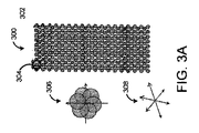
図3Aは、本明細書に開示される実施形態に従って撮像され得るパターン化フローセル300の例示的な構成を示す。この例では、フローセル300が撮像実行中に同時に撮像することができる順序付けられたスポットまたは特徴302の六角形アレイ(304参照)でパターン化される。説明を容易にするために、フローセル300は、数十から数百のスポット302を有するものとして示されている。しかしながら、当業者によって理解され得るように、フローセル300は、撮像される数千、数百万、または数十億のスポット302を有し得る。さらに、いくつかの例では、フローセル300が撮像実行中にサンプリングされるスポット302の複数の平面(フォーカス方向に対して実質的にまたは完全に垂直)を含む多層平面試料であってもよい。特定の実施形態においては、フローセル300が、レーンに分割される数百万または数十億のウェルを有し、パターン化されることがある。この特定の実施形態において、フローセルの各ウェルは、合成によるシーケンシングを使用して配列決定される生物学的物質を含み得る。
FIG. 3A shows an exemplary configuration of a
上記で示唆したように、いくつかの例では、パターン化フローセル300を使用して試料を分解するために、必要な分解能を達成するため少なくとも9つの画像が必要とされる。このことは、パターン化されたフローセル300内のナノウェルの六角形のアレイが、ナノウェル間のピッチがタイトである高周波パターンでありかつ分解不可能であるためである。特に、この例では、試料を十分に分解するために必要な画像の数を決定することができる2つの要因がある。
As suggested above, in some examples, at least nine images are required to achieve the required resolution in order to decompose the sample using the patterned
第1の要因は、所望の光通過帯域のコピーの数である。再び図1Bを参照すると、グラフ122は、SIMを使用しない通常の通過帯域を示す。グラフ124は、光通過帯域の1つのコピーが作成される例を示す。これは1次元における解像度を向上させることができ、一方、グラフ126/グラフ306(図3A)は光学通過帯域の3つのコピーが作成される例を示し、これは2次元においてかなり均一な解像度の向上をもたらす。
The first factor is the number of copies of the desired light passband. Seeing FIG. 1B again,
第2の要因は、各光学通過帯域について位相を復調するために使用される画像の数である。理論的には、必要な画像は2 つだけであるが(実部と虚部を得るために)、通常、3 つの画像を使用して、より良いノイズの平均化が得られる。 The second factor is the number of images used to demodulate the phase for each optical passband. Theoretically, only two images are needed (to get the real and imaginary parts), but three images are usually used to get better noise averaging.
画像を空間周波数からフーリエ空間に平行移動させる場合(対物レンズの後焦点面において顕微鏡によって生成された生データの分析はフーリエ分析に基づく)、フーリエ変換は3つの成分または軸を含むことを理解されたい。すなわち、対物レンズの後焦点面における光の回折は、対物レンズの開口数及び照明の平均波長に応じて、横方向(x, y)寸法で約200nm、軸方向(z)寸法で約500nmの最大解像度を規定する回折限界を生成する。従って、パターニングされたフローセル300の画像においてナノウェルの六角形アレイを使用する場合、SIMを使用して3つの角度で画像が撮影される。また、上記でも説明したように、必要な解像度を得るためには、3つの角度の各々において3つの位相にわたって画像を取得しなければならず、この場合、撮像領域上の全ての部分が観察されることを確実にするために(すなわち、SIMパターンの波長全体をカバーするために)、3つの位相が必要とされ、それによって、9つの画像が得られる。この結果、3つの軸308すべてにおいて解像度が向上する。
It is understood that the Fourier transform involves three components or axes when translating the image from spatial frequency into Fourier space (the analysis of the raw data generated by the microscope in the posterior focal plane of the objective is based on Fourier analysis). sea bream. That is, the diffraction of light on the back focal plane of the objective lens is about 200 nm in the lateral (x, y) dimension and about 500 nm in the axial (z) dimension, depending on the numerical aperture of the objective lens and the average wavelength of illumination. Generates a diffraction limit that defines the maximum resolution. Therefore, when using a nanowell hexagonal array in the image of the patterned
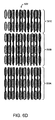
しかしながら、1つの例では、ナノウェル312が正方形アレイ(314を参照)上にパターニングされる、別のタイプのパターニングされたフローセル、例えばフローセル310を使用すると、増大された分解能を達成するためには2つの角度のみが、必要であり、増大された分解能は正方形アレイの軸に沿って位置合わせされる。グラフ316は、光通過帯域の2つのコピーのみが生成され、必要とされる解像度増加を達成するために必要とされる、この例を示す。言い換えれば、フローセル310などの正方形パターン化フローセルはSIMパターンまたは縞を、分解能の増加が望まれる方向に、この場合、正方形アレイの2つの軸(xおよびy)に沿って整列させることによって分解することができる。隣接するナノウェル312間の任意の対角経路に沿って、対角線的に隣接するナノウェルが互いに分解可能になるように、ある程度の分解能向上があることが理解され得る。しかしながら、x軸とy軸に沿ったナノウェル312の間では、ピッチ(Px、Py)はSIMを使用して解像度をブーストする必要があるほど狭く、すなわち、x軸とy軸の空間周波数が高すぎて解決できない。
However, in one example, another type of patterned flow cell, such as the
フローセル310のような正方形のパターン化されたフローセルを使用することによって、SIMを使用する従来のシーケンシングシステムの次元要件を1次元だけ低減することができ、そこでは、分解能が2つの軸318のみで増加する。すなわち、それぞれ3つの位相にわたって3つの角度をカバーする9つの画像を捕捉するのではなく、フローセル310内に含まれる試料を適切に分解するためには、それぞれ3つの位相にわたって2つの角度をカバーする6つの画像のみを捕捉する必要がある。このことは、フローセル310の充填密度の減少にもかかわらず有利である。例えば、充填密度の減少は、同じピッチを有する六角形アレイ上でわずか11%であり得る。しかしながら、様々な実施例に従ってSIMを実施すると、700nmピッチの非SIM六角形アレイに対して、例えば、350nmピッチの正方形パターン化アレイに関して例えば356%の充填密度増加をもたらすことができる。
By using a square patterned flow cell, such as the
さらに別のタイプのパターン化フローセル、この例では非対称にパターン化されたフローセルを使用することによって、SIMを使用する従来のシーケンシングシステムの次元要件を、さらにもう1次元低減することができる。図3Cは、ナノウェルが非対称にパターン化された、パターン化フローセル320を示す。この実施態様では、各ナノウェル322が細長い構造を形成するように成形または構成される。本明細書で利用されるように、細長い構造という用語は、第1の軸に沿った寸法が第2の軸に沿った寸法よりも大きい形状を指す。この例では、x軸が、別の軸(この例ではy軸)に沿ったナノウェル322の長さまたは高さよりも狭い。図3Cに示される実施形態は楕円形ナノウェルを使用するが、他の種類の細長いナノウェル、例えば長方形のナノウェルを使用してもよいことは理解されるべきである。1つの軸のみに沿った試料がSIMを使用した解像度増加と関連付けられるパターンをもたらす、任意の形状のナノウェルを使用することができる。いくつかの実施形態では、パターン化特徴の寸法である縞幅wは、円形特徴の直径、正方形特徴の一辺の長さ、矩形特徴の長辺または短辺の長さ、その長軸または短軸に沿った楕円形特徴の直径、または特徴の1つの軸(例えば、x軸またはy軸)に沿った不規則形状特徴の最長寸法と少なくとも実質的に等しく又はこれらよりもわずかに大きくすることができる。いくつかの実施態様では、ナノウェルが代わりに、正方形または円形として形成されてもよいが、それらの間に非対称の間隔を有する可能性がある。様々な実施形態では、非対称にパターン化されたフローセルは、一次周波数成分がゼロ周波数成分から異なる距離にあるアレイ、その単位格子が様々なピッチによって画定され得るアレイ、またはアレイの周波数成分が従来の3角度SIM OTFよりも非対称である光学伝達関数によって分解され得るアレイを指すことができる。
Yet another type of patterned flow cell, in this example an asymmetrically patterned flow cell, can be used to further reduce the dimensional requirements of traditional sequencing systems that use SIM. FIG. 3C shows a
このようにして、試料は1つの方向または軸に沿って、すなわち、y軸に沿って分解することができ、一方、別の方向または軸に沿って、すなわち、x軸に沿って、SIMは、試料を分解するために分解能を増加させるために使用される。すなわち、x軸に沿って、非対称的にパターン化されたフローセル320のピッチPxは狭くまたはタイトであり、解像度の増大を伴い、一方、y軸に沿って、非対称的にパターン化されたフロー320のピッチPyはより大きくなる。従って、解像度は1つの軸318に沿って/一方向にのみ増加し、フローセル320のナノウェル内に含まれる試料を適切に解像するために、3つの画像のみが捕捉される。したがって、グラフ352によって示されるように、光通過帯域の1つのコピーのみが、生成され、解像度を増加させるために必要とされる。
In this way, the sample can be degraded along one direction or axis, i.e. along the y-axis, while the SIM is along the other direction or axis, i.e. along the x-axis. , Used to increase the resolution to decompose the sample. That is, the pitch P x of the asymmetrically patterned
図4は、正方形または非対称にパターン化されたフローセルを使用して試料をシーケンシングするために、図2の構造化照明撮像システム200などのシーケンシングシステムにおいて実行することができる例示的な動作を示すフローチャートである。動作400において、第1の位相に配向された第1の光学回折格子パターンに対応する光源をオンにすることができる。動作410では、第1の配向における光学回折格子パターンが試料上に投影され、画像が捕捉される。すなわち、図2に戻って参照すると、発光器250は、コリメーションレンズ251によってコリメートされた光線を出力することができる。平行光は、光構造化光学アセンブリ255によって構造化(パターン化)され、ダイクロイックミラー260によって対物レンズ242を介して、ステージ270上に配置された試料容器210の試料上に向けられる。この実施態様では、試料容器210が、正方形または非対称パターンを有するパターン化フローセル、例えばフローセル310または320をそれぞれ含む(図3Bおよび3C)。蛍光試料の場合、正方形または非対称にパターン化されたフローセルに含まれる試料は、構造化された励起光に応答して蛍光を発し、得られた光は、対物レンズ242によって収集され、カメラシステム240のイメージセンサに導かれて、蛍光を検出する。
FIG. 4 illustrates an exemplary operation that can be performed in a sequencing system such as the Structured
動作420では、追加の位相シフトが必要であるかどうかを判定するためにチェックを実行することができる。必要であれば、動作430において、光学回折格子が位相シフトされ、動作は動作410に戻り、そこで光学回折格子パターン(位相シフトされた)が試料上に投影され、画像が捕捉される。前述のように、3つの位相シフトは一般に、撮像領域全体、この実施形態では、正方形パターン化フローセルの領域全体を捕捉するために実行される。
In
追加の位相シフトが必要でない場合には、動作440において、追加の角度が必要であるか否かを判断するためにチェックを実行することができ、動作450において光学回折格子の角度が変更される。動作は動作410に戻り、そこで、(角度を変化させた後の)光学回折格子パターンが試料上に投影され、画像が捕捉される。動作は動作420に進み、ここで、420において追加の位相シフトが必要とされる場合、光回折格子は、動作430において位相シフトされる。再度、動作は動作410に戻り、そこで、(新しい角度および新しい位相での)光学回折格子パターンが試料上に投影され、画像が捕捉される。この場合も、この実施形態では、正方形のパターン化フローセルの全体領域を捕捉するために、3つのフェーズにわたる画像が必要とされる。構造化照明画像システム200のシステム動作の態様を制御するために使用される上記コントローラは、上述の機能を実行するための命令、例えば、使用されている特定のタイプのフローセルを撮像するために、光学回折格子パターンの追加の位相シフトまたは配向が必要であるか否かをチェックする命令で構成することができることを理解されたい。
If no additional phase shift is required, in motion 440 a check can be performed to determine if an additional angle is needed and in
正方形のパターン化されたフローセル、例えばフローセル310(図3)の場合、フローセル310の2つの軸に沿って解像度を増加させるために、2つの角度での画像が必要である。従って、2つの角度(光回折格子パターンの3つの位相シフトにわたる)に対応する2つの方位に投影された光回折格子パターンで画像を取り込んだ後、動作460において(6つの合計画像を組み合わせ、それらを実空間に再変換することによって)高解像度画像が再構成される。この高解像度画像再構成はシステム内で行うことができ、またはいくつかの例では、別個の処理エンティティを使用して再構成を実行することができる。
For a square patterned flow cell, such as the flow cell 310 (FIG. 3), an image at two angles is needed to increase the resolution along the two axes of the
パターン化フローセルが非対称フローセルである実施態様では、上述の方法は角度を変更することを必要としない。さらに、非対称フローセルでは、SIMが1つの軸のみに沿って分解能を増加させるために使用される。したがって、光回折格子は3回だけ位相シフトさせる必要があり、3つの位相シフトについて画像を捕捉することができる。従って、一旦動作420において他の位相シフトが必要とされないと、本方法は動作460に進み、ここで、3つの捕捉画像のみを使用して高解像度画像を再構成することができる。
In embodiments where the patterned flow cell is an asymmetric flow cell, the method described above does not require changing the angle. In addition, in asymmetric flow cells, SIM is used to increase resolution along only one axis. Therefore, the optical diffraction grating needs to be phase-shifted only three times, and images can be captured for the three phase shifts. Thus, once no other phase shift is required in
前述のように、低減された次元のSIM実装の利点を得ることができる特にパターン化されたフローセルを使用する場合、TDIライン走査などのライン走査技術を使用して、それらのパターン化されたフローセルに含まれる試料を撮像することができる。図5は、様々な実施形態において試料を撮像するために使用され得る例示的な2チャネルライン走査撮像システム500を示すブロック図である。
As mentioned earlier, those patterned flow cells using line scanning techniques such as TDI line scanning, especially when using patterned flow cells that can take advantage of the reduced dimension SIM implementation. The sample contained in can be imaged. FIG. 5 is a block diagram illustrating an exemplary 2-channel line
図2の構造化照明撮像システム200の場合のように、ライン走査撮像システム500は核酸の配列決定のために使用することができ、ここで、核酸はアレイ中の固定された位置(すなわち、フローセル320のようなフローセルのウェル)に付着され、そしてアレイは繰り返し撮像され得る。そのような実施態様では、ライン走査撮像システム500が、特定のヌクレオチド塩基型を別のものから区別するために使用され得る2つの異なるカラーチャネルで画像を取得し得る。より具体的には、ライン走査撮像システム500が撮像サイクルにおける画像の所与のスポット箇所についてのベースコール(例えば、アデニン(A)、シトシン(C)、グアニン(G)、またはチミン(T))を決定するプロセスを一般に指す、「ベースコーリング」と呼ばれるプロセスを実施することができる。2チャネルベースコールの間、2つの画像から抽出された画像データは、2つの画像の強度の組み合わせとしてベース同一性を符号化することによって、4つのベースタイプのうちの1つの存在を決定するために使用されてもよい。2つの画像のそれぞれにおける所与のスポットまたは位置について、信号同一性の組合せが[on、on]、[on、off]、[off、on]、または[off、off]であるかどうかに基づいて、ベース同一性を決定することができる。
As in the case of the structured
再びライン走査撮像システム500を参照すると、システムは、その中に配置された2つの光源511および512を備えたライン生成モジュールLGC 510を含む。光源511および512は、レーザビームを出力するレーザダイオードなどのコヒーレント光源であってもよい。光源511は第1の波長(例えば、赤色波長)の光を放射することができ、光源512は第2の波長(例えば、緑色波長)の光を放射することができる。レーザ源511及び512から出力される光線は、1つ以上のビーム成形レンズ513を介して方向付けられ得る。幾つかの実施形態では、単一の光成形レンズを使用して、両方の光源から出力される光線を整形することができる。他の実装形態では、各光ビームに対して別個のビーム成形レンズを使用してもよい。いくつかの例では、ビーム成形レンズが光線がラインパターンに整形されるように、パウエルレンズである。LGC 510または他の光学部品撮像システムのビーム成形レンズは、光源511および512によって放出された光を(例えば、1つ以上のパウエルレンズ、または他のビーム成形レンズ、回折または散乱部品を使用することによって)ラインパターンに成形するように構成される。例えば、幾つかの実施形態では、光源511および512によって放射された光は、光回折格子を通して送られ、試料上に投影することができる光回折格子パターン(SIMパターン)を生成することができる。
Referring again to the line
LGC 510は、単一のインターフェースポートを通して放射光学モジュール(EOM)530に光線を向けるように構成されたミラー514および半反射ミラー515をさらに含んでもよい。光線は、シャッタ要素516を通過してもよい。EOM 530は、対物レンズ535と、対物レンズ535をターゲット550に近づけたり遠ざけたりするように長手方向に移動させるzステージ536とを含むことができる。例えば、ターゲット(例えば、パターン化フローセル)550は、液体層552および半透明カバープレート551を含むことができ、生物学試料は、半透明カバープレートの内側表面、及び液体層の下に位置する基材層の内側表面に位置することができる。次いで、zステージは、フローセルのいずれかの内側表面上に光線を集束させる(例えば、生物学試料上に集束させる)ように、対物レンズを移動させてもよい。生物学試料は、DNA、RNA、タンパク質、または当該分野で既知の光学的配列決定に応答する他の生物学的材料であり得る。
The
EOM 530は、フォーカス追跡モジュール(FTM)540から放射されたフォーカス追跡光線をターゲット550に反射させ、次いで、ターゲット550から戻された光をFTM 540に反射させるために、半反射ミラー533を含んでもよい。FTM 540は、戻されたフォーカス追跡光線の特性を検出し、ターゲット550上の対物レンズ535のフォーカスを最適化するためのフィードバック信号を生成するために、フォーカス追跡光学センサを含んでもよい。
The
EOM 530はまた、ターゲット550から戻された光が通過することを可能にしながら、対物レンズ535を通して光を導くために半反射ミラー534を含んでもよい。いくつかの実施態様では、EOM 530がチューブレンズ532を含むことができる。チューブレンズ532を透過した光は、フィルタ要素531を通過し、カメラアセンブリ520内に入ることができる。カメラアセンブリ520は入射光ビーム(例えば、光源511および512から受け取った赤色光および緑色光に応答する蛍光)に応答して生物学試料から放出される光を検出するために、1つ以上の光学センサ521(例えば、TDIライン走査センサ)を含み得る。一例では、LGC(上述したものなど)が回折格子を通して光を投影し、線状縞模様を生成してもよい。
The
カメラアセンブリ520のセンサからの出力データは、リアルタイム分析回路525に通信されてもよい。リアルタイム分析回路525は様々な実装形態で、画像データを分析し(例えば、画像品質スコアリング、塩基コールなど)、ビームの特性(例えば、フォーカス、形状、強度、電力、明るさ、位置)をグラフィカルユーザインターフェース(GUI)などに報告または表示するためのコンピュータ可読命令を実行する。これらの動作は下流の分析時間を最小限に抑え、撮像実行中にリアルタイムのフィードバックおよびトラブルシューティングを提供するために、撮像サイクル中にリアルタイムで実行することができる。実施形態において、リアルタイム分析回路525は、撮像システム500に通信的に連結され、撮像システム500を制御する計算装置(例えば、計算装置1100)であってもよい。以下でさらに説明する実施態様では、リアルタイム分析回路525が、カメラアセンブリ520から受け取った出力画像データの歪みを補正するためのコンピュータ可読命令をさらに実行することができる。
The output data from the sensor of the
図6A〜6Cは非対称にパターン化されたフローセルのTDIライン走査の例示的表現を表す。ここで、SIMはフローセルの1つの軸に沿って分解能を増加させるために使用される。特に、図6Aは、SIMパターン630が上に重ね合わされた、非対称にパターン化されたフローセル620(非対称にパターン化されたフローセル320(図3C)の実施であり得る)を図示する。TDIライン走査は、非対称的にパターン化されたフローセル620の行ごとの画像をキャプチャするために、y軸に沿って実行され得る。図6Aでキャプチャされた画像は、第1の位相でSIMパターン630によってキャプチャされる。
Figures 6A-6C represent an exemplary representation of the TDI line scan of an asymmetrically patterned flow cell. Here, SIM is used to increase the resolution along one axis of the flow cell. In particular, FIG. 6A illustrates an asymmetrically patterned
例として、ライン走査撮像システム500はシステムの光学系と協調してLGC 510を使用して、赤色スペクトル内の波長を有する光で試料をライン走査し(SIMパターン、すなわち、光学回折格子パターンで重ね合わされる)、緑色カラースペクトル内の波長を有する光で試料をライン走査することができる。ライン走査に応答して、試料の異なるスポットに位置する蛍光色素が蛍光を発することができ、得られた光は、対物レンズ535によって収集することができ、蛍光を検出するためにカメラアセンブリ520の画像センサに向けることができる。例えば、各スポットの蛍光は、カメラアセンブリ520の数画素によって検出することができる。次いで、カメラアセンブリ520から出力された画像データは処理のために、例えば、スワスを形成するために画像を結合するために、リアルタイム分析回路525に通信されてもよい。
As an example, the line-
図6Bは、SIMパターン630を重ね合わせた非対称にパターン化されたフローセル620を示す。しかしながら、図6Bでは、SIMパターン630がx軸に沿って(試料を分解するための分解能増加を必要とする軸と整列して)位相シフトされている。上述のように、ライン走査撮像システム500は、システムの光学系と協調してLGC 510を使用して、試料をライン走査する(位相シフトされたSIMパターン630と重ね合わされる)。画像は、捕捉され、カメラアセンブリ520から出力され、再び、処理のためにリアルタイム分析回路525に通信され得る。
FIG. 6B shows an asymmetrically patterned
図6Cは、SIMパターン630を重ね合わせた非対称にパターン化されたフローセル620を示す。図6Cでは、SIMパターン630がx軸に沿って(試料を分解するための解像度増加を必要とする軸と整列する)第3の位相に位相シフトされている。ここでも、ライン走査撮像システム500は、システムの光学系と協調してLGC 510を使用して、試料をライン走査にすることができる(位相シフトされたSIMパターン630と重ね合わされる)。画像はカメラアセンブリ520から捕捉され、出力され、再び、処理のためにリアルタイム分析回路525に通信され得る。各位相/位相シフトに従って捕捉された画像は、リアルタイム分析回路525によって単一の画像に組み合わされ、実空間に再変換されて、この例ではx軸に沿って、より高い分解能を有する画像を生成することができる。
FIG. 6C shows an asymmetrically patterned
別の実施形態では図6Dに示されるように、フローセル620の異なる部分はその異なる位相においてSIMパターン630でオーバーレイされ得る。すなわち、第1の位相630AのSIMパターンがフローセル620の下部に沿ってオーバーレイされ、第2の位相630Bの同じSIMパターンがフローセル620の中間部分に沿ってオーバーレイされ、また、第3の位相630Cの同じSIMパターンがフローセル620の上部に沿ってオーバーレイされる。したがって、ラインスキャンイメージングシステム500はSIMパターンの異なる位相(630A〜630B)にオーバーレイされたフローセル620をライン走査し、その結果、ラインスキャンイメージングシステム500は、SIMパターンの各必要な位相に従って、単一の実行でフロー全体を撮像することができる。幾つかの実施形態では、ラインスキャンイメージングシステム500は、複数のLGCおよび複数のカメラまたはセンサ/カメラアセンブリを有するように修正することができ、例えばそれら3つの各々はSIMパターンの3つの位相を生成するために、3つの光学回折格子(同じであるが異なる位相で配向されている)を通して光を生成および出力する。このようにして、各カメラまたはセンサ/カメラアセンブリは、異なるSIMパターン位相とともに、フローセル620の画像を同時に捕捉することができる。
In another embodiment, as shown in FIG. 6D, different parts of the
上記で示唆したように、さらに他の実装形態では、SIMパターンが静止したままである間に、試料/フローセルを移動させることができる。TDIライン走査を実施する場合、試料/フローセルは既に移動している。したがって、試料/フローセルのこの移動を活用して、SIMパターンをシフトする必要を回避することができる。すなわち、静止SIMパターンに対する試料/フローセルの移動は、試料を分解するために必要とされる必要な位相を生成する。 As suggested above, in yet other embodiments, the sample / flow cell can be moved while the SIM pattern remains stationary. When performing a TDI line scan, the sample / flow cell has already moved. Therefore, this movement of the sample / flow cell can be leveraged to avoid the need to shift the SIM pattern. That is, the movement of the sample / flow cell with respect to the static SIM pattern produces the required phase required to decompose the sample.
図7は、六角形アレイパターン化フローセル300(図3A)と同様の別の例示的なパターン化フローセル720を示す。従来の構造化照明撮像システムでは、フローセル720が、例えばy軸の方向にライン走査され得る。LGC、例えば、LGC 510(図5)によってフローセル720内の試料上に出力される光線の強度は、x軸に沿って幅広で均一であるように示されている(図示されていないが、ライン走査方向に実質的にまたは正確に垂直である)。しかし、y軸に沿っては、光線の強度は狭い。レーザビームがフローセル720に対して移動するときに、蛍光画像はライン走査カメラまたはセンサ、例えば、カメラアセンブリ520(図5)によって、光線によって照射されている対応する領域に捕捉される。
FIG. 7 shows another exemplary patterned
しかしながら、試料/フローセル720が既に移動しているという事実を利用し、また、非対称にパターン化されたフローセル、例えばフローセル320(図3C)内の試料を解像するためには、1次元SIMのみが必要であるため、SIMパターンを生成する光学回折格子を依然として維持することができる。すなわち、試料を適切に分解するために必要な複数(例えば、3つ)の位相が必要であった。従って、従来のライン走査撮像システムにおいて、例えば光学回折格子を移動(例えば回転又は平行移動)させるのに必要な移動ステージ又は他の要素は、この実施形態においては必要とされない。
However, to take advantage of the fact that the sample /
図8は、静止光学回折格子を使用する、例示的ライン走査撮像システム800を示す。説明を容易にするために、図8は、すべての特徴/元素が示されているわけではない簡略化された図であることに留意されたい。しかしながら、ライン走査システム800は、得られた光学回折格子パターン/SIMパターンを依然として維持するために静止光学回折格子を使用するライン走査撮像システム500の1つの実施形態であってもよい。
FIG. 8 shows an exemplary line
図8の例では、発光体、例えばレーザ802は、コリメーションレンズ804によってコリメートされた光線を出力するように構成される。一実施形態では、レーザ802が緑色波長の光を放射する。平行光は、ダイクロイックフィルタ806によって静止光回折格子812を通って、別のダイクロイックフィルタ828を介して、対物レンズ830に向かい、試料容器832の試料上に向けられる。この実施態様では、試料容器830がフローセル320(図3C)などの非対称にパターン化されたフローセルである。
In the example of FIG. 8, the illuminant, eg, the
第2の発光体、例えばレーザ808は、静止光回折格子812を通って対物レンズ830に、また、ダイクロイックフィルタ828を通って、試料容器832の試料上に、(例えば、赤色波長の)光を放射する。試料容器832は、レーザ802および808からの光線に対して試料容器832を移動させることができるステージ840上に配置される。蛍光試料の場合、試料は構造化された励起光(レーザ802および808からのレーザビーム)に応じて蛍光を発し、得られた光は、対物レンズ828によって集められ、カメラ814および820のイメージセンサに向けられる。
A second illuminant, such as the
ダイクロイックフィルタ806は、レーザ802からの緑色光ビームを通過させて静止光回折格子812に通過させ、一方、レーザ808からの赤色光ビームを静止光回折格子812に向けて反射させるために使用される。ダイクロイックフィルタ828は、レーザ802および808からの赤色光ビームおよび緑色光ビームが対物レンズ830に反射されることを可能にし、一方、カメラ814および820が緑色光および赤色光で蛍光発光された画像をそれぞれ捕捉することを可能にするという点で、同様に機能する。ダイクロイックフィルタ816は蛍光試料からの緑色光放射をカメラ814に向け、ダイクロイックフィルタ822は蛍光試料からの赤色光放射をカメラ820に向ける。レンズ818および824は、それぞれ、カメラ814および820のためのコリメートレンズである。ダイクロイックミラー826は、蛍光を発した試料からの緑色および赤色光放射を適切なカメラに向ける。
The
ライン走査システム800では、光回折格子812は静止している。すなわち、先に議論したように、非対称にパターン化されたフローセルをSIMと併用することによって、構造化された照明の1次元のみが必要とされ、フローセルに沿ってビームを移動させることによって、複数の位相を達成することができる。換言すれば、試料/フローセルに対するレーザビームの移動、またはレーザビームに対する試料/フローセルの移動の結果、試料と干渉縞の励起パターンとの間の相対的な移動は、全て、異なる位相を生成するために必要なものである。
In the
図9は、ライン走査システム800などのライン走査撮像システムで線走査され得るパターン化フローセル920を示す。フローセル920に光学回折格子パターンを投影することができ、一方、フローセル920は、ライン走査撮像技術に従って移動する。静止光回折格子パターンに対するフローセル920の移動は、前述のように、必要な位相シフトを生成し、ライン走査中に捕捉された画像は、いったん組み合わせて実空間に再変換すると、分解能を増加させる。
FIG. 9 shows a
特に、光線はy軸の方向に移動する。ここでも、光ビームの強度はx軸(図示せず)に沿って均質であるが、静止した光回折格子、例えば、静止光回折格子、例えば静止光回折格子(図8)を通過することによってy軸に沿った強度が変調される。光線がフローセル920に対して移動するときに、光回折格子パターンはシフトする。実際には、3つ超、または数十もの位相シフトを生成することができる。その結果、光回折格子の代わりに試料/フローセル920を移動させることによって、ライン走査の軸に沿った分解能の増加を達成することができる。いくつかの実施態様では上述したように、この方向の解像度は、ランダム特徴または周期的パターンの両方を有する表面上で少なくとも2倍増加させることができる。解像度は、例えば少なくとも2倍増加させることができるので、フローセル920内のナノウェルの密度は、2倍以上増加させることができることを理解されたい。
In particular, the rays move in the y-axis direction. Again, the intensity of the light beam is homogeneous along the x-axis (not shown), but by passing through a stationary light diffraction grating, such as a static light diffraction grating, such as a static light diffraction grating (FIG. 8). The intensity along the y-axis is modulated. The light diffraction grating pattern shifts as the light beam travels relative to the
図10は非対称的にパターン化されたフローセルを使用して試料をシーケンシングするために、ライン走査撮像システム500(図5)またはライン走査撮像システム800(図8)などの、ライン走査撮像システムにおいて実施され得る操作を例示するフローチャートである。動作1000において、第1の光回折格子パターン配向に対応する、静止光回折格子、例えば静止光回折格子812を通して出力される、レーザ源、例えばレーザ源802および808からの光ビームをオンにすることができる。動作1010では光回折格子パターンが試料上に投影され、動作1020では試料はライン走査される。ライン走査は、ライン走査撮像システム800(図8)に関して前述したように実施されてもよい。操作1030では、試料が、前述のライン走査技術に従って移動されるか、または指向された光が試料と光回折格子パターンとの間の相対運動を達成するために、前述のように移動されてもよい。
Figure 10 shows in a line-scanning imaging system, such as the line-scanning imaging system 500 (FIG. 5) or the line-scanning imaging system 800 (FIG. 8), to sequence samples using asymmetrically patterned flow cells. It is a flowchart which illustrates the operation which can be performed. In
動作1020および1030は、サンプル全体を表す画像を取り込むために必要な回数だけ繰り返されてもよい。ここでも、試料が静止光学回折格子パターンに対して移動された結果、試料及び光学回折格子パターンの画像を、分解能を高めるために必要とされる必要な位相シフトにわたって捕捉することができる。操作1040において、高解像度画像を再構成することができる。
Operations 1020 and 1030 may be repeated as many times as necessary to capture an image representing the entire sample. Again, as a result of the sample being moved relative to the static optical grating pattern, images of the sample and the optical grating pattern can be captured over the necessary phase shifts required to increase resolution. In
ライン走査中に光回折格子パターンと試料との間のモーションブラーを防止するために、レーザ源はパルス状に動作することができることに留意されたい。すなわち、レーザ源、例えば、レーザ源802および808は、励起毎にライン走査画像を捕捉することができるようにパルス化されてもよい。幾つかの実施形態では、試料/フローセルに対する光回折格子パターンの方位を90°ずらすことができる。他の実装では、図6A〜6Cに例示されているように、光回折格子パターンの方位が試料が明暗の領域にわたって移動しないようなものである場合(光回折格子パターンの方位が90°ずれた場合の場合のように)、光回折格子パターンに対する試料の移動が同じ縞強度を通って移動するので、レーザ光源のパルス化が不要となる場合がある。
Note that the laser source can behave in a pulsed manner to prevent motion blur between the light diffraction grating pattern and the sample during line scanning. That is, the laser sources, such as the
本明細書に記載された実施形態は主として、回折格子を使用して、撮像される試料上に投影される縞パターンを生成するという文脈で説明されてきたが、実施形態では投影された縞パターンが必ずしも回折格子によって生成される必要はないことに留意されたい。正弦波縞パターンを生成する任意の方法が適切であり得る。縞模様の生成は、所望の干渉パターンの点で相互にコヒーレントな2つの逆伝播ビーム間の干渉を介して、回折格子のコヒーレントまたは非コヒーレント撮像を介して、ビームスプリッタを経て分離され干渉されたビームを介して、ライトパイプまたは導波路等の中の逆伝播ビームを介して達成することができる。 The embodiments described herein have been described primarily in the context of using a diffraction grating to generate a fringe pattern projected onto the sample to be imaged, but in embodiments the projected fringe pattern has been described. Note that is not necessarily generated by the grating. Any method of generating a sinusoidal fringe pattern may be appropriate. The fringe formation was split and interfered through a beam splitter via coherent or non-coherent imaging of the grating via interference between two backpropagating beams that were coherent to each other in terms of the desired interference pattern. It can be achieved via a beam and via a backpropagation beam in a light pipe or waveguide or the like.
図11は、システム200、500、および/または800に実装され、本明細書で説明される、図4および図10に示される方法の1つ以上の態様の前述の特徴および機能性など、本明細書で開示されるシステムおよび方法の様々な特徴を実装するために使用され得る例示的なコンピューティング成分を示す。例えば、コンピューティング要素は、リアルタイム分析回路525として実装されてもよい。
FIG. 11 is implemented in
本明細書で使用されるように、回路という用語は、本出願の1つ以上の実施形態に従って実行することができる機能の所与のユニットを記述することができる。本明細書で使用されるように、回路は、任意の形態のハードウェア、またはハードウェアとソフトウェアとの組み合わせを利用して実装され得る。例えば、1つ以上のプロセッサ、コントローラ、ASIC、PLA、PAL、CPLD、FPGA、論理コンポーネント、ソフトウェアルーチン、又は他のメカニズムが、回路を構成するために実装され得る。実施形態において、本明細書で説明される様々な回路は個別の回路として実装されてもよく、又は説明される機能及び構成が1つ以上の回路の間で部分的に又は全体的に共有されてもよい。言い換えれば、本明細書を読んだ後の当業者は、本明細書に記載された様々な特徴および機能性が任意の所与のアプリケーションにおいて実装されてもよく、様々な組合せおよび順列で1つ以上の別個のまたは共有の回路において実装されてもよいことを理解することができる。機能の様々な特徴または要素は個別のモジュールとして個別に説明または請求され得るが、当業者はこれらの特徴および機能が1つ以上の共通のソフトウェアおよびハードウェア要素の間で共有され得ることを理解し、そのような説明はそのような特徴または機能を実装するために、個別のハードウェアまたはソフトウェア構成要素が使用されることを必要とせず、または暗示するものではない。 As used herein, the term circuit can describe a given unit of function that can be performed according to one or more embodiments of the present application. As used herein, circuits can be implemented using any form of hardware, or a combination of hardware and software. For example, one or more processors, controllers, ASICs, PLAs, PALs, CPLDs, FPGAs, logic components, software routines, or other mechanisms may be implemented to form a circuit. In embodiments, the various circuits described herein may be implemented as separate circuits, or the functions and configurations described may be partially or wholly shared between one or more circuits. You may. In other words, those skilled in the art after reading this specification may implement the various features and functionality described herein in any given application, one in various combinations and permutations. It can be understood that it may be implemented in the above separate or shared circuits. Various features or elements of a feature may be described or claimed individually as separate modules, but those skilled in the art understand that these features and features may be shared between one or more common software and hardware elements. However, such description does not require or imply that separate hardware or software components will be used to implement such features or features.
アプリケーションの構成要素または回路がソフトウェアを使用して全体的にまたは部分的に実装される場合、一実装形態では、これらのソフトウェア要素がそれに関して説明された機能を実行することが可能なコンピューティングまたは処理モジュールで動作するように実装され得る。そのようなコンピューティングコンポーネントの一例を図13に示す。様々な実装が、この例示的コンピューティング要素1000に関して記述される。この説明を読んだ後、他のコンピューティングモジュールまたはアーキテクチャを使用してアプリケーションをどのように実装するかが、当業者には明らかになるであろう。
When an application component or circuit is implemented entirely or partially using software, in one implementation, these software elements are capable of performing the functions described in that computing or It can be implemented to work with processing modules. An example of such a computing component is shown in FIG. Various implementations are described for this
ここで図13を参照すると、コンピューティング要素1000は例えば、デスクトップ、ラップトップ、ノート型パソコン、およびタブレットコンピュータ内で見られるコンピューティングまたは処理能力、ハンドヘルドコンピューティングデバイス(タブレット、PDA、スマートフォン、携帯電話、パームトップなど)、メインフレーム、スーパーコンピュータ、ワークステーション、若しくはサーバ、又は所与のアプリケーションまたは環境にとって望ましくまたは適切であり得る任意の他の種類の専用または汎用コンピューティングデバイスを表すことができる。コンピューティング要素1000はまた、所与の装置内に組み込まれた、又は所与の装置で利用可能な計算能力を表すこともできる。例えば、コンピューティング要素は例えば、デジタルカメラ、ナビゲーションシステム、携帯電話、ポータブルコンピューティングデバイス、モデム、ルータ、WAP、端末、および何らかの形態の処理能力を含み得る他の電子デバイスなどの他の電子デバイスに見出され得る。
With reference to FIG. 13, the
コンピューティング要素1000は、例えばプロセッサ1004のような1つ以上のプロセッサ、コントローラ、制御モジュールまたは他の処理装置を含むことができる。プロセッサ1004は、例えばマイクロプロセッサ、コントローラ、または他の制御ロジックなどの汎用または専用処理エンジンを使用して実装され得る。図示の例では、プロセッサ1004はバス1002に接続されているが、任意の通信媒体を使用して、コンピューティング要素1000の他の要素との相互作用を容易にしたり、外部と通信したりすることができる。
The
コンピューティング要素1000はまた、ここでは単にメインメモリ1008と称される1つ以上のメモリモジュールを含んでもよい。例えば、好ましくは、ランダムアクセスメモリ(RAM)または他のダイナミック・メモリが、プロセッサ1004によって実行される情報および命令を記憶するために使用されてもよい。メインメモリ1008は、プロセッサ1004によって実行される命令の実行中に、一時変数又は他の中間情報を記憶するためにも使用され得る。コンピューティング要素1000は同様に、プロセッサ1004のための静的情報および命令を記憶するために、バス1002に結合された読出し専用メモリ(“ROM”)または他の静的記憶装置を含むことができる。
The
コンピューティング要素1000は、例えば媒体ドライブ1012および記憶ユニットインタフェース1020を含むことができる、1つ以上の様々な形態の情報記憶機構1010を含むこともできる。媒体ドライブ1012は、固定又は取り外し可能な記憶媒体1014をサポートするためのドライブ又は他の機構を含んでもよい。例えば、ハードディスクドライブ、ソリッドステートドライブ、磁気テープドライブ、光ディスクドライブ、CD若しくはDVDドライブ(RまたはRW)、または他の取り外し可能な若しくは固定媒体ドライブが提供され得る。したがって、記憶媒体1014は例えば、ハードディスク、ソリッドステートドライブ、磁気テープ、カートリッジ、光ディスク、CD、DVD若しくはBlu-ray、または媒体ドライブ1012によって読み取られたり、そこに書き込まれたり若しくはそこからアクセスされる他の固定若しくは取り外し可能媒体を含むことができる。これらの例が示すように、記憶媒体1014は、コンピュータソフトウェア又はデータが記憶されたコンピュータ使用可能な記憶媒体を含むことができる。
The
代替例では、情報記憶機構1010がコンピュータプログラムまたは他の命令またはデータをコンピューティング要素1000にロードすることを可能にする他の同様の手段を含むことができる。そのような手段は例えば、固定又は取り外し可能な記憶ユニット1022及びインターフェース1020を含み得る。このような記憶ユニット1022およびインターフェース1020の例は、プログラムカートリッジおよびカートリッジインタフェース、取り外し可能なメモリ(例えば、フラッシュメモリまたは他の取り外し可能なメモリモジュール)およびメモリスロット、PCMCIAスロットおよびカード、ならびにソフトウェアおよびデータが記憶ユニット1022からコンピューティング要素1000に転送されることを可能にする他の固定または取り外し可能記憶ユニット1022およびインターフェース1020を含むことができる。
Alternatives can include other similar means that allow the
コンピューティング要素1000は、通信インターフェース1024を含むこともできる。通信インターフェース1024は、ソフトウェアおよびデータがコンピューティング要素1000と外部装置との間で転送されることを可能にするために使用されてもよい。通信インターフェース1024の例は、モデムまたはソフトモデム、ネットワークインターフェース(イーサネット(登録商標)、ネットワークインターフェースカード、WiMedia、IEEE 802.XXまたは他のインターフェースなど)、通信ポート(USBポート、IRポート、RS232ポートBluetooth(登録商標)インターフェース、または他のポートなど)、または他の通信インターフェースを含み得る。通信インターフェース1024を介して転送されるソフトウェア及びデータは、典型的には所与の通信インターフェース1024によって交換されることが可能な、電子的、電磁気的(光を含む)、又は他の信号であり得る、信号上で搬送され得る。これらの信号は、チャネル1028を介して通信インターフェース1024に提供されてもよい。このチャネル1028は、信号を搬送することができ、有線又は無線通信媒体を使用して実装することができる。チャネルのいくつかの例は、電話回線、セルラリンク、RFリンク、光リンク、ネットワークインターフェース、ローカル又はワイドエリアネットワーク、及び他の有線又は無線通信チャネルを含むことができる。
The
本明細書では、用語「コンピュータ可読媒体」、「コンピュータ使用可能媒体」および「コンピュータプログラム媒体」は一般に、例えば、メモリ1008、記憶ユニット1022、および媒体1014などの揮発性または不揮発性の非一時的媒体を指すために使用される。これらおよび他の様々な形態のコンピュータプログラム媒体またはコンピュータ使用可能媒体は、実行のために1つ以上の命令の1つ以上の配列を処理デバイスに搬送することに関与することができる。媒体に具体化されるそのような命令は一般に、「コンピュータプログラムコード」または「コンピュータプログラム製品」(コンピュータプログラムまたは他のグループの形態でグループ化することができる)と呼ばれる。このような命令が実行されると、コンピューティング要素1000は本明細書で論じるように、本願の特徴または機能を実行することができる。
As used herein, the terms "computer readable medium", "computer usable medium" and "computer program medium" are generally volatile or non-volatile, non-transitory such as memory 1008, storage unit 1022, and medium 1014. Used to refer to a medium. These and various other forms of computer program or computer-enabled media can be involved in transporting one or more sequences of one or more instructions to a processing device for execution. Such instructions embodied in the medium are commonly referred to as "computer program code" or "computer program products" (which can be grouped in the form of computer programs or other groups). When such an instruction is executed, the
様々な実施例および実施形態に関して上述したが、個々の実施形態の1つ以上に記載されている様々な特徴、態様および機能性は、それらが記載されている特定の実施例への利用可能性に制限されず、その代わりに、そのような実施形態が記載されているかどうか、およびそのような特徴が記載されている実施形態の一部であるとして提示されているかどうかにかかわらず、本願の1つ以上の他の実施形態に単独で、または様々な組み合わせで利用できることが理解されるべきである。したがって、本願の幅および範囲は、上述の例示的な実施形態のいずれによっても限定されるべきではない。 Although described above for various embodiments and embodiments, the various features, embodiments and functionality described in one or more of the individual embodiments are available for the particular embodiment in which they are described. Not limited to, and instead, whether such embodiments are described and whether such features are presented as part of the described embodiments of the present application. It should be understood that it can be used alone or in various combinations for one or more other embodiments. Therefore, the width and scope of the present application should not be limited by any of the exemplary embodiments described above.
前述の概念のすべての組み合わせ(そのような概念が相互に矛盾しない限り)は、本明細書で開示される本発明の主題の一部であると考えられることを理解されたい。特に、本開示の末尾にある特許請求の範囲の主題のすべての組み合わせは、本明細書に開示される本発明の主題の一部であると考えられる。 It should be understood that all combinations of the aforementioned concepts (unless such concepts contradict each other) are considered to be part of the subject matter of the invention disclosed herein. In particular, all combinations of claims at the end of this disclosure are considered to be part of the subject matter of the invention disclosed herein.
特許請求の範囲を含む、本開示全体にわたって使用される「実質的に」および「約」という用語は処理の変動などによる小さな変動を記述し、説明するために使用される。例えば、これらの用語は、±5%以下、例えば±2%以下、例えば±1%以下、例えば±0.5%以下、例えば±0.2%以下、例えば±0.1%以下、例えば±0.05%以下を指すことができる。 The terms "substantially" and "about" used throughout the present disclosure, including the claims, are used to describe and explain small variations, such as due to variations in processing. For example, these terms refer to ± 5% or less, for example ± 2% or less, for example ± 1% or less, for example ± 0.5% or less, for example ± 0.2% or less, for example ± 0.1% or less, for example ± 0.05% or less. Can be done.
適用可能な範囲で、本明細書における用語「第1」、「第2」、「第3」などは、単に、これらの用語によって説明されるそれぞれの目的を別個のエンティティとして示すために使用され、本明細書において明示的に別段の記載がない限り、時系列順の意味を暗示することを意味しない。 To the extent applicable, the terms "first," "second," "third," etc. herein are used merely to indicate the respective purposes described by these terms as separate entities. , Unless expressly stated otherwise in this specification, does not imply the meaning of chronological order.
本書で使用されている用語及び語句、ならびにそれらのバリエーションは別途明示的に記載されていない限り、限定ではなく、オープンエンド型の意味にとる必要がある。前述の例として、「含む」という用語は「限定なしに含む」などを意味するものとして解釈されるべきであり、「例」という用語は論議中のアイテムの例を提供するために使用され、そのリストを網羅的または限定するものではなく、「1つの(“a”または“an”)」という用語は「少なくとも1つ」、は「1つ以上」などを意味するものとして解釈されるべきであり、「従来の」、「伝統的な」、「通常の」、「標準の」、「既知の」などの形容詞、および同様の意味の用語は記載されたアイテムを、所与の期間に、または所与の時間に利用可能なアイテムに限定するものと解釈されるべきではなく、代わりに、現在または将来において利用可能であるか、または知られている可能性がある従来の、伝統的な、通常の、または標準の技術を包含するものと解釈されるべきである。同様に、本明細書が当業者に明らかであるか、または知られている可能性がある技術に言及する場合、そのような技術は、現在または将来の任意の時点で当業者に明らかであるか、または知られている技術を包含する。 The terms and phrases used in this document, as well as their variations, should be taken in an open-ended sense, not limited, unless explicitly stated otherwise. As an example above, the term "contains" should be construed to mean "contain without limitation", etc., and the term "example" is used to provide an example of the item under discussion. The list is not exhaustive or limiting, and the term "one (" a "or" an ")" should be construed to mean "at least one", "one or more", etc. Adjectives such as "traditional," "traditional," "ordinary," "standard," and "known," and terms with similar meanings, have items listed for a given period of time. , Or should not be construed as limiting to items available at a given time, instead traditional, traditional, which may be available or known now or in the future. Should be construed as embracing ordinary or standard techniques. Similarly, if this specification refers to a technique that is or may be known to those of skill in the art, such technique will be apparent to those of ordinary skill in the art at any time in the present or future. Or include known techniques.
場合によっては、「1つ以上」、「少なくとも」、「少なくとも」又は「ただし、これらに限定されない」などの拡張語および句、または他の同様の句の存在は、そのような拡張語句が存在しない可能性がある場合に、より狭い場合が意図され、または必要とされることを意味すると解釈されるべきではない。 In some cases, the existence of extended words and phrases such as "one or more", "at least", "at least" or "but not limited to", or other similar phrases, such extended words exist. It should not be construed to mean that a narrower case is intended or required if it may not.
さらに、本明細書で説明される様々な実装形態は、例示的なブロック図、フローチャートおよび他の図に関して説明される。本明細書を読んだ後、当業者には明らかになるように、例示された実施形態およびそれらの様々な代替形態は、例示された例に限定されることなく実施することができる。例えば、ブロック図及びそれらの付随する説明は、特定のアーキテクチャ又は構造を指定するものとして解釈されるべきではない。 In addition, the various implementations described herein are described with reference to exemplary block diagrams, flowcharts and other diagrams. As will be apparent to those skilled in the art after reading this specification, the illustrated embodiments and their various alternatives can be practiced without limitation to the illustrated examples. For example, block diagrams and their accompanying descriptions should not be construed as specifying a particular architecture or structure.
本開示のさまざまな実施形態が上述されてきたが、それらは限定ではなく、例としてのみ提示されてきたことが理解されるべきである。同様に、様々な図は、本開示に含まれ得る特徴および機能を理解するのを助けるために行われる、本開示のための例示的なアーキテクチャまたは他の構成を示すことができる。本開示は例示されたアーキテクチャまたは構成に限定されるものではないが、所望の特徴は種々の代替アーキテクチャおよび構成を使用して実施することができる。実際、本開示の所望の特徴を実施するために、代替の機能的、論理的、または物理的なパーティションおよび構成をどのように実施することができるかは、当業者には明らかであろう。また、本明細書に示されたもの以外の多数の異なる構成要素名を、様々なパーティションに適用することができる。さらに、フロー図、動作説明、および方法クレームに関して、本明細書でステップが提示される順序は、文脈が別段の指示をしない限り、様々な実施形態が、列挙された機能を同じ順序で実行するように実装されることを強制するものではない。
Although various embodiments of the present disclosure have been described above, it should be understood that they have been presented as examples, not limitations. Similarly, various diagrams can show exemplary architectures or other configurations for this disclosure that are made to aid in understanding the features and functions that may be included in this disclosure. The present disclosure is not limited to the illustrated architecture or configuration, but the desired features can be implemented using a variety of alternative architectures and configurations. In fact, it will be apparent to those skilled in the art how alternative functional, logical, or physical partitions and configurations can be implemented to implement the desired features of the present disclosure. Also, many different component names other than those shown herein can be applied to the various partitions. In addition, with respect to flow diagrams, operating instructions, and method claims, the order in which the steps are presented herein is such that various embodiments perform the listed functions in the same order, unless the context dictates otherwise. It does not force it to be implemented as such.
Claims (18)
投影される前記光学パターンを前記生物学試料に対して位相シフトし、位相シフトされるとともに前記生物学試料上でオーバーレイされる前記光学パターンの少なくとも第2画像を捕捉する位相シフトステップと、
捕捉される前記第1画像及び捕捉される少なくとも前記第2画像に基づいて、前記生物学試料を表す高解像度画像を再構成する再構成ステップと、
を含む、生物学試料を撮像する方法であり、
前記生物学試料は、複数の細長いナノウェルを含み非対称にパターンされるフローセルに含まれ、
前記複数の細長いナノウェルのそれぞれは、楕円形状に成形され又は矩形状に成形される、方法。 A projection step of projecting an optical pattern onto a biological sample and capturing a first image of the optical pattern overlaid on the biological sample.
A phase shift step of phase-shifting the projected optical pattern with respect to the biological sample and capturing at least a second image of the optical pattern that is phase-shifted and overlaid on the biological sample.
A reconstruction step of reconstructing a high resolution image representing the biological sample based on the captured first image and at least the captured second image.
Is a method of imaging biological samples, including
The biological sample is contained in an asymmetrically patterned flow cell containing a plurality of elongated nanowells.
A method in which each of the plurality of elongated nanowells is formed into an elliptical shape or a rectangular shape .
前記生物学試料上に投影される前記光学パターンは、前記光学回折格子を通る前記光が生成する光学回折格子パターンであり、
前記位相シフトステップは、前記光学回折格子を位相シフトすることを含む、請求項4に記載の方法。 Further comprising directing light to an optical diffraction grating of first phase and first angular orientation and passing through the optical diffraction grating.
The optical pattern projected onto the biological sample is an optical diffraction grating pattern generated by the light passing through the optical diffraction grating.
The method of claim 4 , wherein the phase shift step comprises phase shifting the optical diffraction grating.
前記高解像度画像を再構成する前に、前記光学回折格子の第3位相シフトを実行し、光学回折格子パターンを前記生物学試料上に投影し、位相シフトされるとともに前記生物学試料上でオーバーレイされる前記光学回折格子パターンの少なくとも第3画像を捕捉することと、
をさらに含み、
前記生物学試料上に投影される前記光学パターンは、前記光学回折格子を通る前記光が生成する光学回折格子パターンであり、
前記位相シフトステップは、前記光学回折格子を位相シフトすることを含む、請求項1に記載の方法。 Directing the light toward the optical diffraction grating of the first phase and the first angle orientation, and passing through the optical diffraction grating,
Prior to reconstructing the high resolution image, a third phase shift of the optical grating is performed to project the optical grating pattern onto the biological sample, which is phase shifted and overlaid on the biological sample. Capturing at least a third image of the optical diffraction grating pattern to be performed
Including
The optical pattern projected onto the biological sample is an optical diffraction grating pattern generated by the light passing through the optical diffraction grating.
The method of claim 1, wherein the phase shift step comprises phase shifting the optical diffraction grating.
前記光学回折格子を通る前記光が生物学試料上に生成する光学回折格子パターンを投影し、前記生物学試料上でオーバーレイされる前記光学回折格子パターンの第1画像を捕捉する投影ステップと、
前記光学回折格子を位相シフトし、前記光学回折格子パターンを前記生物学試料上に投影し、位相シフトされるとともに前記生物学試料上でオーバーレイされる前記光学回折格子パターンの少なくとも第2画像を捕捉する第2画像捕捉ステップと、
前記光学回折格子を第2角度配向に再配向させ、前記光学回折格子パターンを前記生物学試料上に投影し、前記生物学試料上でオーバーレイされる前記光学回折格子パターンの第3画像を捕捉する第3画像捕捉ステップと、
前記光学回折格子を位相シフトし、前記光学回折格子パターンを前記生物学試料上に投影し、位相シフトされるとともに前記生物学試料上でオーバーレイされる前記光学回折格子パターンの少なくとも第4画像を捕捉する第4画像捕捉ステップと、
捕捉される、前記第1画像、前記少なくとも前記第2画像、前記第3画像及び前記少なくとも前記第4画像に基づいて、前記生物学試料を表す高解像度画像を再構成する再構成ステップと、
を含む、生物学試料を撮像する方法であり、
前記生物学試料は、複数の細長いナノウェルを含み非対称にパターンされるフローセルに含まれ、
前記複数の細長いナノウェルのそれぞれは、楕円形状に成形され又は矩形状に成形される、方法。 The alignment step of directing the light to the optical diffraction grating of the first phase and the first angle orientation and passing through the optical diffraction grating,
A projection step of projecting an optical diffraction grating pattern generated on a biological sample by the light passing through the optical diffraction grating and capturing a first image of the optical diffraction grating pattern superimposed on the biological sample.
The optical diffraction grating is phase-shifted, the optical diffraction grating pattern is projected onto the biological sample, and at least a second image of the optical diffraction grating pattern that is phase-shifted and overlaid on the biological sample is captured. The second image capture step and
The optical diffraction grating is reoriented to a second angular orientation, the optical diffraction grating pattern is projected onto the biological sample, and a third image of the optical diffraction grating pattern superimposed on the biological sample is captured. The third image capture step and
The optical diffraction grating is phase-shifted, the optical diffraction grating pattern is projected onto the biological sample, and at least a fourth image of the optical diffraction grating pattern that is phase-shifted and overlaid on the biological sample is captured. 4th image capture step and
A reconstruction step of reconstructing a high resolution image representing the biological sample based on the captured first image, at least the second image, the third image, and at least the fourth image.
Is a method of imaging biological samples, including
The biological sample is contained in an asymmetrically patterned flow cell containing a plurality of elongated nanowells.
A method in which each of the plurality of elongated nanowells is formed into an elliptical shape or a rectangular shape .
放射される前記光線が通過すると光学回折格子パターンを生成するように適合される光学回折格子と、
生物学試料上でオーバーレイされる光学回折格子パターンの複数の画像を捕捉するように適合されるカメラアセンブリと、
前記複数の画像の組み合わせに基づいて、前記生物学試料を表す高解像度画像を再構成するように適合されるプロセッサと、
を備えるシステムであり、
前記複数の画像は、前記光学回折格子の前記生物学試料に対する3つの位相を反映し、
前記生物学試料は、非対称アレイに配向される複数のナノウェルを含むフローセルに配置され、
前記複数のナノウェルのそれぞれは、楕円形状に成形され、又は矩形状に成形される、システム。 A laser source that emits light rays and
An optical grating that is adapted to produce an optical grating pattern when the emitted rays pass through,
With a camera assembly adapted to capture multiple images of the optical grating pattern overlaid on the biological sample,
A processor adapted to reconstruct a high resolution image representing the biological sample based on the combination of the plurality of images.
It is a system equipped with
The plurality of images reflect the three phases of the optical diffraction grating with respect to the biological sample .
The biological sample is placed in a flow cell containing multiple nanowells oriented in an asymmetric array.
A system in which each of the plurality of nanowells is formed into an elliptical shape or a rectangular shape .
放射される前記光線が通過すると光学回折格子パターンを生成するように適合される光学回折格子と、
生物学試料上でオーバーレイされる光学回折格子パターンの複数の画像を捕捉するように適合されるカメラアセンブリと、
前記複数の画像の組み合わせに基づいて、前記生物学試料を表す高解像度画像を再構成するように適合されるプロセッサと、
を備えるシステムであり、
前記複数の画像は、前記光学回折格子の前記生物学試料に対する3つの位相を反映し、
前記生物学試料は、非対称アレイに配向される複数のナノウェルを含むフローセルに配置され、
前記複数のナノウェルのそれぞれは、楕円形状に成形され、又は矩形状に成形され、
前記カメラアセンブリは、時間遅延積分ライン走査カメラアセンブリを備える、システム。 A laser source that emits light rays and
An optical grating that is adapted to produce an optical grating pattern when the emitted rays pass through,
With a camera assembly adapted to capture multiple images of the optical grating pattern overlaid on the biological sample,
A processor adapted to reconstruct a high resolution image representing the biological sample based on the combination of the plurality of images.
It is a system equipped with
The plurality of images reflect the three phases of the optical diffraction grating with respect to the biological sample.
The biological sample is placed in a flow cell containing multiple nanowells oriented in an asymmetric array.
Each of the plurality of nanowells is formed into an elliptical shape or a rectangular shape.
The camera assembly comprises a time delay integration line scanning camera assembly .
前記フローセルの様々な部分が、オーバーレイされ、前記光学回折格子の前記3つの位相を同時に表す、請求項13に記載のシステム。 The biological sample is contained in a flow cell and
13. The system of claim 13 , wherein the various parts of the flow cell are overlaid to simultaneously represent the three phases of the optical diffraction grating.
前記3つの位相ステップ素子のそれぞれは、放射される前記光線が前記位相ステップ素子を通過すると光学回折格子パターンを生成するように適合され、
前記カメラアセンブリは、前記3つの位相ステップ素子のそれぞれが生成するとともに生物学試料上でオーバーレイされる光学回折格子パターンの画像を捕捉するように適合される、請求項13に記載のシステム。 The optical diffraction grating includes three phase step elements.
Each of the three phase step elements is adapted to generate an optical grating pattern when the emitted light beam passes through the phase step element.
13. The system of claim 13 , wherein the camera assembly is adapted to capture an image of an optical grating pattern generated by each of the three phase step elements and overlaid on a biological sample.
前記3つのイメージセンサのそれぞれは、前記位相ステップ素子のそれぞれが生成する前記光学回折格子パターンの前記画像を捕捉するように適合される、請求項15に記載のシステム。 The camera assembly comprises three image sensors.
15. The system of claim 15 , wherein each of the three image sensors is adapted to capture the image of the optical diffraction grating pattern generated by each of the phase step elements.
放射される前記光線が通過すると光学回折格子パターンを生成するように適合される光学回折格子と、
生物学試料上でオーバーレイされる光学回折格子パターンの複数の画像を捕捉するように適合されるカメラアセンブリと、
前記複数の画像の組み合わせに基づいて、前記生物学試料を表す高解像度画像を再構成するように適合されるプロセッサと、
を備えるシステムであり、
前記複数の画像は、前記光学回折格子の前記生物学試料に対する3つの位相と、前記光学回折格子の前記生物学試料に対する2つの角度配向とを反映し、
前記生物学試料は、非対称アレイに配向される複数のナノウェルを含むフローセルに配置され、
前記複数のナノウェルのそれぞれは、楕円形状に成形され、又は矩形状に成形される、システム。 A laser source that emits light rays and
An optical grating that is adapted to produce an optical grating pattern when the emitted rays pass through,
With a camera assembly adapted to capture multiple images of the optical grating pattern overlaid on the biological sample,
A processor adapted to reconstruct a high resolution image representing the biological sample based on the combination of the plurality of images.
It is a system equipped with
The plurality of images reflect the three phases of the optical diffraction grating with respect to the biological sample and the two angular orientations of the optical diffraction grating with respect to the biological sample .
The biological sample is placed in a flow cell containing multiple nanowells oriented in an asymmetric array.
A system in which each of the plurality of nanowells is formed into an elliptical shape or a rectangular shape .
17. The system of claim 17, wherein each of the plurality of nanowells is oriented along the first and second axes of the flow cell to improve resolution of information representing the biological sample.
Priority Applications (1)
| Application Number | Priority Date | Filing Date | Title |
|---|---|---|---|
| JP2021128321A JP7250862B2 (en) | 2018-01-24 | 2021-08-04 | Dimension-reducing structured illumination microscopy with patterned arrays of nanowells |
Applications Claiming Priority (5)
| Application Number | Priority Date | Filing Date | Title |
|---|---|---|---|
| US201862621564P | 2018-01-24 | 2018-01-24 | |
| US62/621,564 | 2018-01-24 | ||
| NL2020622A NL2020622B1 (en) | 2018-01-24 | 2018-03-20 | Reduced dimensionality structured illumination microscopy with patterned arrays of nanowells |
| NL2020622 | 2018-03-20 | ||
| PCT/US2019/014574 WO2019147581A1 (en) | 2018-01-24 | 2019-01-22 | Reduced dimensionality structured illumination microscopy with patterned arrays of nanowells |
Related Child Applications (1)
| Application Number | Title | Priority Date | Filing Date |
|---|---|---|---|
| JP2021128321A Division JP7250862B2 (en) | 2018-01-24 | 2021-08-04 | Dimension-reducing structured illumination microscopy with patterned arrays of nanowells |
Publications (3)
| Publication Number | Publication Date |
|---|---|
| JP2021505842A JP2021505842A (en) | 2021-02-18 |
| JP2021505842A5 JP2021505842A5 (en) | 2021-08-05 |
| JP6926246B2 true JP6926246B2 (en) | 2021-08-25 |
Family
ID=67395706
Family Applications (2)
| Application Number | Title | Priority Date | Filing Date |
|---|---|---|---|
| JP2019571725A Active JP6926246B2 (en) | 2018-01-24 | 2019-01-22 | Dimensional reduced structured illumination microscope with nanowell patterned array |
| JP2021128321A Active JP7250862B2 (en) | 2018-01-24 | 2021-08-04 | Dimension-reducing structured illumination microscopy with patterned arrays of nanowells |
Family Applications After (1)
| Application Number | Title | Priority Date | Filing Date |
|---|---|---|---|
| JP2021128321A Active JP7250862B2 (en) | 2018-01-24 | 2021-08-04 | Dimension-reducing structured illumination microscopy with patterned arrays of nanowells |
Country Status (15)
| Country | Link |
|---|---|
| US (3) | US11150455B2 (en) |
| EP (1) | EP3628090B1 (en) |
| JP (2) | JP6926246B2 (en) |
| KR (2) | KR102478948B1 (en) |
| CN (1) | CN111052147A (en) |
| AU (2) | AU2019211231B2 (en) |
| BR (1) | BR112019027617A2 (en) |
| CA (1) | CA3066734C (en) |
| IL (1) | IL271120A (en) |
| MX (1) | MX2019014522A (en) |
| NL (1) | NL2020622B1 (en) |
| NZ (1) | NZ759785A (en) |
| RU (1) | RU2740776C1 (en) |
| TW (1) | TWI718457B (en) |
| WO (1) | WO2019147581A1 (en) |
Families Citing this family (9)
| Publication number | Priority date | Publication date | Assignee | Title |
|---|---|---|---|---|
| NL2020622B1 (en) | 2018-01-24 | 2019-07-30 | Lllumina Cambridge Ltd | Reduced dimensionality structured illumination microscopy with patterned arrays of nanowells |
| NL2020623B1 (en) * | 2018-01-24 | 2019-07-30 | Illumina Inc | Structured illumination microscopy with line scanning |
| US20220120687A1 (en) * | 2019-02-04 | 2022-04-21 | Life Technologies Holdings Pte Ltd | Method of analyzing samples, analyzing device and computer program |
| WO2021205356A1 (en) * | 2020-04-08 | 2021-10-14 | Perseus Biomics | Space time imaging system and method |
| US11492662B2 (en) | 2020-08-06 | 2022-11-08 | Singular Genomics Systems, Inc. | Methods for in situ transcriptomics and proteomics |
| KR102451422B1 (en) | 2020-11-24 | 2022-10-07 | 울산과학기술원 | Method and apparatus for simulataneous acquisition of super-resolution image and fast widefield image |
| TWI751893B (en) * | 2021-01-21 | 2022-01-01 | 晶相光電股份有限公司 | Image sensing device |
| KR102583469B1 (en) * | 2021-11-05 | 2023-09-26 | 연세대학교 산학협력단 | Optical Imaging Apparatus and Method for Retrieval of High Frequency Components Using Nanophotonic Device |
| WO2024006284A1 (en) * | 2022-07-01 | 2024-01-04 | Illumina Cambridge Limited | Multiband scanning and fiber bundle to enable reduced light source intensity and improved imaging quality |
Family Cites Families (87)
| Publication number | Priority date | Publication date | Assignee | Title |
|---|---|---|---|---|
| US3856986A (en) | 1968-12-06 | 1974-12-24 | American Express Invest | Scanned holography systems using temporal modulation |
| US4213706A (en) | 1977-08-19 | 1980-07-22 | The University Of Arizona Foundation | Background compensating interferometer |
| US5761085A (en) | 1996-11-12 | 1998-06-02 | The United States Of America As Represented By The Secretary Of The Navy | Method for monitoring environmental parameters at network sites |
| US7133726B1 (en) * | 1997-03-28 | 2006-11-07 | Applera Corporation | Thermal cycler for PCR |
| US6188478B1 (en) | 1998-10-21 | 2001-02-13 | Philips Electronics North America Corporation | Method and apparatus for film-thickness measurements |
| CN1292227A (en) | 1999-10-09 | 2001-04-25 | 胡嘉鹏 | Preparation process of amino acid wheat flavour milk tea |
| JP4994560B2 (en) | 2000-08-25 | 2012-08-08 | アムニス コーポレイション | Speed measurement of small moving objects such as cells |
| JP4675011B2 (en) | 2001-09-25 | 2011-04-20 | 株式会社リコー | Shape measuring method and shape measuring apparatus |
| US7274446B2 (en) | 2001-04-07 | 2007-09-25 | Carl Zeiss Jena Gmbh | Method and arrangement for the deep resolved optical recording of a sample |
| JP5048899B2 (en) | 2001-09-28 | 2012-10-17 | オリンパス株式会社 | microscope |
| US6947127B2 (en) | 2001-12-10 | 2005-09-20 | Carl Zeiss Jena Gmbh | Arrangement for the optical capture of excited and/or back scattered light beam in a sample |
| US6737634B2 (en) * | 2002-01-16 | 2004-05-18 | The University Of Chicago | Use of multiple optical vortices for pumping, mixing and sorting |
| KR100489431B1 (en) | 2002-06-28 | 2005-05-12 | 학교법인연세대학교 | Phase-shifting profilometry system using scanning and measuring method thereof |
| US20080316575A1 (en) * | 2002-08-01 | 2008-12-25 | The University Of Chicago., | Aberration correction of optical traps |
| JP2005080181A (en) | 2003-09-03 | 2005-03-24 | Nikon Corp | Image reading apparatus and image reading program |
| US7532323B2 (en) | 2003-10-28 | 2009-05-12 | Cha-Min Tang | Spatial light modulator apparatus and method |
| WO2005079544A2 (en) | 2004-02-19 | 2005-09-01 | Cyvera Corporation | Multi-well plate with alignment grooves for encoded microparticles |
| US20050221351A1 (en) | 2004-04-06 | 2005-10-06 | Affymetrix, Inc. | Methods and devices for microarray image analysis |
| NO20051850A (en) | 2005-04-15 | 2006-09-25 | Sinvent As | Infrared detection of gas - diffractive. |
| CN1292227C (en) | 2005-07-12 | 2006-12-27 | 中国科学院上海光学精密机械研究所 | Method for calibrating space resolution ratio of high-resolution digital interference instrument |
| CN101466998B (en) | 2005-11-09 | 2015-09-16 | 几何信息学股份有限公司 | The method and apparatus of absolute-coordinate three-dimensional surface imaging |
| US7803609B2 (en) | 2006-07-21 | 2010-09-28 | Affymetrix, Inc. | System, method, and product for generating patterned illumination |
| DE102006044229B4 (en) | 2006-09-20 | 2023-09-28 | Carl Zeiss Microscopy Gmbh | Method and device for image processing with higher harmonics of a lighting grid |
| DE102006047912A1 (en) | 2006-10-06 | 2008-04-10 | Carl Zeiss Microimaging Gmbh | Method and device for parallelized microscopic imaging |
| JP5136422B2 (en) | 2006-12-12 | 2013-02-06 | 株式会社ニコン | Microscope device and image processing method |
| US8252581B2 (en) * | 2007-01-22 | 2012-08-28 | Wafergen, Inc. | Apparatus for high throughput chemical reactions |
| DE102007009550B4 (en) | 2007-02-27 | 2008-12-18 | Ludwig-Maximilian-Universität | Method and microscope device for observing a moving sample |
| US20080240543A1 (en) | 2007-03-30 | 2008-10-02 | Wolfgang Ernst Gustav Budach | Calibration and normalization method for biosensors |
| GB0707433D0 (en) | 2007-04-18 | 2007-05-23 | Stfc Science & Technology | Fluorescence measurement |
| US8691164B2 (en) | 2007-04-20 | 2014-04-08 | Celula, Inc. | Cell sorting system and methods |
| WO2009009081A2 (en) | 2007-07-10 | 2009-01-15 | Massachusetts Institute Of Technology | Tomographic phase microscopy |
| US8759077B2 (en) | 2007-08-28 | 2014-06-24 | Lightspeed Genomics, Inc. | Apparatus for selective excitation of microparticles |
| US8222040B2 (en) | 2007-08-28 | 2012-07-17 | Lightspeed Genomics, Inc. | Nucleic acid sequencing by selective excitation of microparticles |
| CN101918789A (en) | 2007-09-16 | 2010-12-15 | 梅厄·本-利维 | Imaging measurements system with periodic pattern illumination and TDI |
| US8509879B2 (en) | 2007-11-06 | 2013-08-13 | The Regents Of The University Of California | Apparatus and method for widefield functional imaging (WiFI) using integrated structured illumination and laser speckle imaging |
| US8537461B2 (en) * | 2007-11-26 | 2013-09-17 | Carl Zeiss Microimaging Gmbh | Method and configuration for the optical detection of an illuminated specimen |
| US20090219607A1 (en) | 2008-01-17 | 2009-09-03 | Baylor College Of Medicine | Method and apparatus for enhanced resolution microscopy of living biological nanostructures |
| DE102008009216A1 (en) | 2008-02-13 | 2009-08-20 | Carl Zeiss Microimaging Gmbh | Apparatus and method for spatially high resolution imaging of a structure of a sample |
| US7994485B2 (en) * | 2008-04-08 | 2011-08-09 | Carestream Health, Inc. | Apparatus and method for fluorescence measurements using spatially structured illumination |
| WO2009132124A2 (en) * | 2008-04-24 | 2009-10-29 | The Trustees Of Columbia University In The City Of New York | Geometric patterns and lipid bilayers for dna molecule organization and uses thereof |
| EP2286175A4 (en) | 2008-06-03 | 2017-04-12 | Hwan J. Jeong | Interferometric defect detection and classification |
| US7986412B2 (en) * | 2008-06-03 | 2011-07-26 | Jzw Llc | Interferometric defect detection and classification |
| DE102008049878A1 (en) * | 2008-09-30 | 2010-04-01 | Carl Zeiss Microlmaging Gmbh | Improved methods and devices for microscopy with structured illumination |
| US8836948B2 (en) * | 2009-01-29 | 2014-09-16 | The Regents Of The University Of California | High resolution structured illumination microscopy |
| JP2011128019A (en) | 2009-12-17 | 2011-06-30 | Hitachi Maxell Ltd | Microplate device and utilization of the same |
| US9465228B2 (en) | 2010-03-19 | 2016-10-11 | Optical Biosystems, Inc. | Illumination apparatus optimized for synthetic aperture optics imaging using minimum selective excitation patterns |
| US8502867B2 (en) | 2010-03-19 | 2013-08-06 | Lightspeed Genomics, Inc. | Synthetic aperture optics imaging method using minimum selective excitation patterns |
| WO2011135819A1 (en) * | 2010-04-26 | 2011-11-03 | 株式会社ニコン | Structural illumination microscope device |
| US10051240B2 (en) * | 2010-06-14 | 2018-08-14 | Howard Hughes Medical Institute | Structured plane illumination microscopy |
| US20120156100A1 (en) | 2010-12-20 | 2012-06-21 | Industrial Technology Research Institute | Apparatus for single molecule detection and method thereof |
| US9594870B2 (en) | 2010-12-29 | 2017-03-14 | Life Technologies Corporation | Time-warped background signal for sequencing-by-synthesis operations |
| CN103477209B (en) * | 2011-03-01 | 2016-03-30 | 通用电气医疗集团生物科学公司 | For the system and method for phase control of throwing light in fluorescent microscope |
| US8796185B2 (en) | 2011-03-08 | 2014-08-05 | Lightspeed Genomics, Inc. | Self-assembling high density ordered patterned biomolecule array and method for making and using the same |
| US8817362B2 (en) | 2011-04-29 | 2014-08-26 | Lightspeed Genomics, Inc. | Modular pattern illumination and light beam multiplexing for selective excitation of microparticles |
| US8778848B2 (en) | 2011-06-09 | 2014-07-15 | Illumina, Inc. | Patterned flow-cells useful for nucleic acid analysis |
| DE112012002619T5 (en) * | 2011-06-24 | 2014-04-17 | Kla-Tencor Corp. | Method and device for inspecting semiconductor light-emitting elements by means of photoluminescence imaging |
| US9095852B2 (en) * | 2011-08-22 | 2015-08-04 | The Regents Of The University Of California | Multilayer high density microwells |
| KR101211532B1 (en) * | 2011-08-24 | 2012-12-12 | 인하대학교 산학협력단 | Large-scale randomly distributed plasmonic nanowells array and manufacturing method thereof |
| EP2806262A4 (en) * | 2012-01-18 | 2015-09-23 | Nikon Corp | Structured illumination device, structured illumination microscope device, and structured illumination method |
| US9372308B1 (en) * | 2012-06-17 | 2016-06-21 | Pacific Biosciences Of California, Inc. | Arrays of integrated analytical devices and methods for production |
| US9575304B2 (en) * | 2012-06-25 | 2017-02-21 | Huron Technologies International Inc. | Pathology slide scanners for fluorescence and brightfield imaging and method of operation |
| RU2502983C1 (en) * | 2012-08-17 | 2013-12-27 | Игорь Викторович Чеботарь | Method of nanoscopy |
| US10048201B2 (en) | 2012-09-10 | 2018-08-14 | The Trustees Of Princeton University | Fluid channels for computational imaging in optofluidic microscopes |
| DE102012017920B4 (en) * | 2012-09-11 | 2023-11-30 | Carl Zeiss Microscopy Gmbh | Optical arrangement and light microscope |
| DE102012017922B4 (en) * | 2012-09-11 | 2024-03-14 | Carl Zeiss Microscopy Gmbh | Optical arrangement and light microscope |
| DE102012020877A1 (en) * | 2012-10-17 | 2014-04-17 | Carl Zeiss Microscopy Gmbh | Optics arrangement and light microscope |
| EP2917734A4 (en) * | 2012-11-06 | 2016-09-07 | Chemimage Corp | System and method for serum based cancer detection |
| US9426400B2 (en) | 2012-12-10 | 2016-08-23 | Kla-Tencor Corporation | Method and apparatus for high speed acquisition of moving images using pulsed illumination |
| US9831362B2 (en) * | 2013-03-29 | 2017-11-28 | The Hong Kong University Of Science And Technology | Roll-to-roll fabrication of ordered three-dimensional nanostructure array, related techniques, materials and products |
| US9194811B1 (en) | 2013-04-01 | 2015-11-24 | Kla-Tencor Corporation | Apparatus and methods for improving defect detection sensitivity |
| EP2801854B1 (en) | 2013-05-10 | 2017-07-19 | Ruprecht-Karls-Universität Heidelberg | Method and apparatus for combination of localization microscopy and structured illumination microscopy |
| CN105849275B (en) * | 2013-06-25 | 2020-03-17 | 普罗格诺西斯生物科学公司 | Method and system for detecting spatial distribution of biological targets in a sample |
| WO2015022781A1 (en) | 2013-08-15 | 2015-02-19 | コニカミノルタ株式会社 | Cell detection method and cell detection device |
| JP2016008941A (en) | 2014-06-26 | 2016-01-18 | 株式会社日立ハイテクノロジーズ | Defect observation method and defect observation device, as well as detect detection device |
| WO2016001910A1 (en) | 2014-06-29 | 2016-01-07 | OPTICS 3D Ltd. | Dual structured illumination modulated in phase and intensity |
| WO2016027453A1 (en) | 2014-08-18 | 2016-02-25 | 国立大学法人大阪大学 | Raman spectroscopy microscope and method for observing raman scattering |
| WO2016105548A1 (en) * | 2014-12-24 | 2016-06-30 | Lamdagen Corporation | Mobile/wearable devices incorporating lspr sensors |
| WO2016149397A1 (en) | 2015-03-16 | 2016-09-22 | Pacific Biosciences Of California, Inc. | Integrated devices and systems for free-space optical coupling |
| CN107924027B (en) * | 2015-06-12 | 2024-01-23 | 加利福尼亚太平洋生物科学股份有限公司 | Integrated target waveguide device and system for optical coupling |
| WO2017047735A1 (en) | 2015-09-17 | 2017-03-23 | Agcテクノグラス株式会社 | Cell culture vessel |
| SG10201913394SA (en) | 2015-09-17 | 2020-03-30 | Histide Ag | Pharmaceutical association for converting a neoplastic cell into a non-neoplastic cell and uses thereof |
| US20190054461A1 (en) * | 2015-09-30 | 2019-02-21 | University Of Houston System | Multi-use combined micro and nanowell plates |
| WO2017147508A1 (en) * | 2016-02-26 | 2017-08-31 | Sri International | Identification and isolation of antibodies from white blood cells |
| US10900076B2 (en) | 2016-05-18 | 2021-01-26 | Illumina, Inc. | Self assembled patterning using patterned hydrophobic surfaces |
| US10901230B2 (en) | 2016-06-21 | 2021-01-26 | Illumina, Inc. | Super-resolution microscopy |
| CN114921537A (en) | 2017-03-17 | 2022-08-19 | 雅普顿生物系统公司 | Sequencing and high resolution imaging |
| NL2020622B1 (en) | 2018-01-24 | 2019-07-30 | Lllumina Cambridge Ltd | Reduced dimensionality structured illumination microscopy with patterned arrays of nanowells |
-
2018
- 2018-03-20 NL NL2020622A patent/NL2020622B1/en active
- 2018-12-24 TW TW107146788A patent/TWI718457B/en active
-
2019
- 2019-01-22 CA CA3066734A patent/CA3066734C/en active Active
- 2019-01-22 WO PCT/US2019/014574 patent/WO2019147581A1/en unknown
- 2019-01-22 CN CN201980003309.7A patent/CN111052147A/en active Pending
- 2019-01-22 MX MX2019014522A patent/MX2019014522A/en unknown
- 2019-01-22 KR KR1020217035038A patent/KR102478948B1/en active IP Right Grant
- 2019-01-22 EP EP19743894.8A patent/EP3628090B1/en active Active
- 2019-01-22 AU AU2019211231A patent/AU2019211231B2/en active Active
- 2019-01-22 BR BR112019027617-3A patent/BR112019027617A2/en unknown
- 2019-01-22 KR KR1020197037823A patent/KR102321151B1/en active IP Right Grant
- 2019-01-22 US US16/621,122 patent/US11150455B2/en active Active
- 2019-01-22 JP JP2019571725A patent/JP6926246B2/en active Active
- 2019-01-22 RU RU2019140419A patent/RU2740776C1/en active
- 2019-01-22 NZ NZ759785A patent/NZ759785A/en unknown
- 2019-12-02 IL IL271120A patent/IL271120A/en unknown
-
2021
- 2021-08-03 US US17/392,941 patent/US11650156B2/en active Active
- 2021-08-04 JP JP2021128321A patent/JP7250862B2/en active Active
- 2021-10-06 AU AU2021245157A patent/AU2021245157B2/en active Active
-
2023
- 2023-01-13 US US18/154,405 patent/US11933728B2/en active Active
Also Published As
| Publication number | Publication date |
|---|---|
| TW201940411A (en) | 2019-10-16 |
| CA3066734A1 (en) | 2019-08-01 |
| US20230194426A1 (en) | 2023-06-22 |
| WO2019147581A1 (en) | 2019-08-01 |
| AU2021245157A1 (en) | 2021-11-04 |
| CA3066734C (en) | 2023-08-01 |
| AU2019211231B2 (en) | 2021-09-23 |
| EP3628090A1 (en) | 2020-04-01 |
| AU2021245157B2 (en) | 2023-05-18 |
| EP3628090B1 (en) | 2023-01-18 |
| US11650156B2 (en) | 2023-05-16 |
| RU2740776C1 (en) | 2021-01-21 |
| KR20200026202A (en) | 2020-03-10 |
| JP7250862B2 (en) | 2023-04-03 |
| KR20210141719A (en) | 2021-11-23 |
| US20210364772A1 (en) | 2021-11-25 |
| US20200103639A1 (en) | 2020-04-02 |
| NZ759785A (en) | 2022-01-28 |
| AU2019211231A1 (en) | 2020-01-02 |
| US11933728B2 (en) | 2024-03-19 |
| JP2021505842A (en) | 2021-02-18 |
| CN111052147A (en) | 2020-04-21 |
| BR112019027617A2 (en) | 2020-09-01 |
| TWI718457B (en) | 2021-02-11 |
| KR102321151B1 (en) | 2021-11-03 |
| JP2021184100A (en) | 2021-12-02 |
| EP3628090A4 (en) | 2020-05-27 |
| NL2020622B1 (en) | 2019-07-30 |
| US11150455B2 (en) | 2021-10-19 |
| IL271120A (en) | 2020-01-30 |
| MX2019014522A (en) | 2021-02-26 |
| KR102478948B1 (en) | 2022-12-19 |
Similar Documents
| Publication | Publication Date | Title |
|---|---|---|
| JP6926246B2 (en) | Dimensional reduced structured illumination microscope with nanowell patterned array | |
| JP6947855B2 (en) | Structured Illumination Microscopy with Line Scan |
Legal Events
| Date | Code | Title | Description |
|---|---|---|---|
| A621 | Written request for application examination |
Free format text: JAPANESE INTERMEDIATE CODE: A621 Effective date: 20200609 |
|
| A521 | Request for written amendment filed |
Free format text: JAPANESE INTERMEDIATE CODE: A523 Effective date: 20210625 |
|
| A871 | Explanation of circumstances concerning accelerated examination |
Free format text: JAPANESE INTERMEDIATE CODE: A871 Effective date: 20210625 |
|
| A975 | Report on accelerated examination |
Free format text: JAPANESE INTERMEDIATE CODE: A971005 Effective date: 20210629 |
|
| TRDD | Decision of grant or rejection written | ||
| A977 | Report on retrieval |
Free format text: JAPANESE INTERMEDIATE CODE: A971007 Effective date: 20210630 |
|
| A01 | Written decision to grant a patent or to grant a registration (utility model) |
Free format text: JAPANESE INTERMEDIATE CODE: A01 Effective date: 20210706 |
|
| A61 | First payment of annual fees (during grant procedure) |
Free format text: JAPANESE INTERMEDIATE CODE: A61 Effective date: 20210804 |
|
| R150 | Certificate of patent or registration of utility model |
Ref document number: 6926246 Country of ref document: JP Free format text: JAPANESE INTERMEDIATE CODE: R150 |