JP6921611B2 - Process cartridge, image forming device, image forming method - Google Patents
Process cartridge, image forming device, image forming method Download PDFInfo
- Publication number
- JP6921611B2 JP6921611B2 JP2017091436A JP2017091436A JP6921611B2 JP 6921611 B2 JP6921611 B2 JP 6921611B2 JP 2017091436 A JP2017091436 A JP 2017091436A JP 2017091436 A JP2017091436 A JP 2017091436A JP 6921611 B2 JP6921611 B2 JP 6921611B2
- Authority
- JP
- Japan
- Prior art keywords
- discharge
- partial
- bias
- image forming
- charging member
- Prior art date
- Legal status (The legal status is an assumption and is not a legal conclusion. Google has not performed a legal analysis and makes no representation as to the accuracy of the status listed.)
- Active
Links
Images


Landscapes
- Electrostatic Charge, Transfer And Separation In Electrography (AREA)
- Electrophotography Configuration And Component (AREA)
Description
本発明は、帯電部材を介し被帯電体に帯電させる帯電装置を備えた画像形成装置に関するものである。 The present invention relates to an image forming apparatus including a charging device that charges an object to be charged via a charging member.
従来、電子写真方式を採用する画像形成装置には、ドラム型の電子写真感光体(以下、感光ドラムと記す)表面を所定の電位に均一に帯電処理する工程を含んでいる。 Conventionally, an image forming apparatus that employs an electrophotographic method includes a step of uniformly charging the surface of a drum-type electrophotographic photosensitive member (hereinafter referred to as a photosensitive drum) to a predetermined potential.
帯電手段としては、例えばローラ帯電部材(以下、帯電ローラと記す)を感光ドラム表面に当接し、この帯電ローラに電圧を印加して感光ドラムを帯電する接触帯電方式が現在主流となっている。 As a charging means, for example, a contact charging method in which a roller charging member (hereinafter referred to as a charging roller) is brought into contact with the surface of a photosensitive drum and a voltage is applied to the charging roller to charge the photosensitive drum is currently the mainstream.
帯電ローラに対する電圧の印加方法としては直流電圧を印加する方式と、直流電圧に交流電圧を重畳し、プラス側及びマイナス側への放電を交互に起こすことで帯電を均一化する方式がある。後者の方式においては、帯電ローラと感光ドラム間の抵抗性負荷に流れる抵抗負荷電流と、帯電ローラと感光ドラム間の容量性負荷に流れる容量負荷電流と、帯電ローラと感光ドラム間の放電電流とが流れ、これらが合計された電流が帯電ローラに流れる。この際、安定した帯電を得るためには放電電流量を所定値以上にすると良いことが経験的に分かっている。 As a method of applying a voltage to the charging roller, there are a method of applying a DC voltage and a method of superimposing an AC voltage on the DC voltage and alternately causing discharge to the plus side and the minus side to make the charging uniform. In the latter method, the resistance load current flowing through the resistive load between the charging roller and the photosensitive drum, the capacitive load current flowing through the capacitive load between the charging roller and the photosensitive drum, and the discharge current between the charging roller and the photosensitive drum Flows, and the total current flows through the charging roller. At this time, it is empirically known that the amount of discharge current should be set to a predetermined value or more in order to obtain stable charging.
図18に、帯電ローラに交流電圧Vcを印加した際、帯電ローラに流れる電流Ic特性を示す。交流電圧Vcは交流電圧のピーク電圧値、電流Icは交流電流の実効値を示している。図18より、交流電圧Vcの振幅を徐々に上昇させると、これに伴って帯電電流が増加する。所定電圧Vhの2倍以下の場合には、交流電圧の振幅と帯電電流とは略比例している。これは抵抗負荷電流と容量負荷電流とが電圧振幅に比例するとともに、電圧振幅が小さいために放電現象が発生せず放電電流が流れないためである。そして、交流電圧をさらに大きくしていくと、所定電圧Vhの2倍で放電現象が始まる。この時、帯電電流Icは比例関係から外れ、放電電流Is分だけ多く流れる。ここで安定して帯電させるためには、この放電電流Isが所定値以上になるように交流電圧Vcを設定する必要がある。 FIG. 18 shows the current Ic characteristics that flow through the charging roller when an AC voltage Vc is applied to the charging roller. The AC voltage Vc indicates the peak voltage value of the AC voltage, and the current Ic indicates the effective value of the AC current. From FIG. 18, when the amplitude of the AC voltage Vc is gradually increased, the charging current increases accordingly. When the voltage is 2 times or less of the predetermined voltage Vh, the amplitude of the AC voltage and the charging current are substantially proportional to each other. This is because the resistance load current and the capacitance load current are proportional to the voltage amplitude, and because the voltage amplitude is small, the discharge phenomenon does not occur and the discharge current does not flow. Then, when the AC voltage is further increased, the discharge phenomenon starts at twice the predetermined voltage Vh. At this time, the charging current Ic deviates from the proportional relationship and flows as much as the discharge current Is. Here, in order to stably charge the battery, it is necessary to set the AC voltage Vc so that the discharge current Is becomes a predetermined value or more.
しかしながら、感光ドラムへの放電量が増えた場合、感光ドラムの削れ等の感光ドラム劣化を促進するとともに、放電生成物による高温高湿環境での画像流れ等の異常画像が発生する場合があった。よって、安定した帯電を得られ、かつ前記問題を解決するためには、放電量を極力抑えた必要最低限の電圧印加に制御する必要がある。しかし、感光ドラムへの印加電圧と放電量の関係は常に一定ではなく、感光ドラムの感光体層や誘電体層の膜厚、帯電部材や空気の環境変動等により変化する。放電量の変化による不具合は、前述の環境変動による原因の他に、帯電部材の製造ばらつきや汚れによる抵抗値変動、耐久による感光ドラムの静電容量変動、画像形成装置本体の高圧発生装置の特性ばらつきなどでも発生することが判っている。 However, when the amount of discharge to the photosensitive drum increases, deterioration of the photosensitive drum such as scraping of the photosensitive drum is promoted, and abnormal images such as image flow in a high temperature and high humidity environment due to the discharge product may occur. .. Therefore, in order to obtain stable charging and solve the above problems, it is necessary to control the application of the minimum necessary voltage while suppressing the amount of discharge as much as possible. However, the relationship between the voltage applied to the photosensitive drum and the amount of discharge is not always constant, and changes depending on the film thickness of the photosensitive layer and the dielectric layer of the photosensitive drum, the environmental changes of the charging member and the air, and the like. In addition to the above-mentioned causes of environmental fluctuations, defects due to changes in the amount of discharge are caused by variations in the manufacturing of charged members, fluctuations in resistance due to dirt, fluctuations in the capacitance of the photosensitive drum due to durability, and characteristics of the high-voltage generator of the image forming device. It is known that it also occurs due to variations.
このような放電量の変化を抑制するために、「放電電流制御方式」が提案されている(例えば、特許文献1参照)。この方式においては、帯電ローラに印加される交流印加電圧のピーク電圧とその微分波形のピーク電圧を検出し、放電電流値を算出する制御方式が提案されている(特許文献1参照)。 In order to suppress such a change in the amount of discharge, a "discharge current control method" has been proposed (see, for example, Patent Document 1). In this method, a control method has been proposed in which the peak voltage of the AC applied voltage applied to the charging roller and the peak voltage of the differential waveform thereof are detected to calculate the discharge current value (see Patent Document 1).
しかしながら、近年進んでいる画像形成装置の高寿命化や市場における使用方法の多様化に伴って、帯電ローラの画像形成プロセス方向と垂直な方向(以下長手方向)の汚れムラや感光ドラムの長手方向の膜厚ムラが生じてしまう場合があった。これは、例えば長手方向において印字部に偏りがある印刷パターンを出力し続けたり、感光ドラムに記録材が直接当接する方式の画像形成装置で封筒や葉書等の小サイズの記録材を使用し続けたりすること等により起きてしまう場合がある。 However, with the recent progress in extending the life of image forming devices and diversifying the usage methods in the market, uneven stains in the direction perpendicular to the image forming process direction of the charging roller (hereinafter referred to as the longitudinal direction) and the longitudinal direction of the photosensitive drum In some cases, uneven film thickness may occur. This is, for example, continuing to output a print pattern with a bias in the printing portion in the longitudinal direction, or continuing to use a small-sized recording material such as an envelope or a postcard in an image forming apparatus in which the recording material comes into direct contact with the photosensitive drum. It may happen due to such things as.
感光ドラムの長手方向の膜厚ムラや帯電ローラの長手方向の汚れムラが生じると長手方向で帯電ローラから感光ドラムへ電流が流れる際のインピーダンスが異なり放電しやすい部分と放電しにくい部分ができてしまう。この場合、上記放電電流制御方式では長手方向全体の放電量を検知しているため適正より低い放電量になる部分や、適正より高く放電して感光ドラムの削れが促進される部分が存在する場合がある。放電しにくい部分は帯電が不安定になり局所的に放電過剰部と放電不足部が生じてしまい、この放電不足部は現像部により現像されて白地部に黒ポチとなって現れる。この結果、白地に黒ポチが多数出てくる所謂砂地という画像弊害が発生してしまう場合があった。 If uneven film thickness in the longitudinal direction of the photosensitive drum or uneven stain in the longitudinal direction of the charging roller occurs, the impedance when the current flows from the charging roller to the photosensitive drum in the longitudinal direction differs, and there are parts that are easy to discharge and parts that are difficult to discharge. It ends up. In this case, since the discharge current control method detects the entire discharge amount in the longitudinal direction, there is a portion where the discharge amount is lower than the appropriate amount or a portion where the discharge amount is higher than the appropriate value and the scraping of the photosensitive drum is promoted. There is. The part that is difficult to discharge becomes unstable in charging, and an over-discharged part and an under-discharged part are locally generated, and this under-discharged part is developed by the developing part and appears as a black spot on a white background. As a result, there is a case where an image harmful effect called a so-called sandy area in which a large number of black spots appear on a white background occurs.
帯電ローラの汚れムラや感光ドラムの膜厚ムラを事前に予測して放電量を決定すればよいが、このような現象はユーザーの使用状況によって大きく変化するので予測は困難である。 The amount of discharge may be determined by predicting in advance the unevenness of dirt on the charging roller and the unevenness of the film thickness of the photosensitive drum, but such a phenomenon is difficult to predict because it changes greatly depending on the usage conditions of the user.
そこで本発明の目的は、長手方向の放電ムラを検知し、放電量を適正化することのできる画像形成装置、プロセスカートリッジ及び画像形成方法を提供することである。 Therefore, an object of the present invention is to provide an image forming apparatus, a process cartridge, and an image forming method capable of detecting discharge unevenness in the longitudinal direction and optimizing the amount of discharge.
上記目的を達成する為の本発明の構成は、潜像を担持する回転可能な像担持体と、前記像担持体を露光する露光手段と、前記像担持体を帯電する帯電部材と、前記帯電部材にバイアス電圧を印加するバイアス印加手段と、前記帯電部材と前記像担持体との間で放電す
る電流量を検知する放電量検知手段と、前記放電量検知手段によって検知される放電電流量から前記帯電部材に印加するバイアス電圧を決定する放電電流制御手段と、前記帯電部材と前記像担持体との間の放電に関する情報である放電情報を検出する放電情報検出手段とを有し、前記放電情報検出手段は、前記像担持体の面内の印字可能な領域の一部に回転方向に対し垂直な方向の幅が前記印字可能な領域の幅よりも小さい領域を部分測定領域と設定し、前記帯電部材により前記像担持体を一定の電位に帯電した後に前記露光手段によって前記部分測定領域と前記部分測定領域を除く領域とで互いに異なる電位を形成している時に前記部分測定領域と前記帯電部材との間の放電に関する部分放電情報を検出し、前記放電電流制御手段は、該部分放電情報に基づいて前記帯電部材に印加される画像形成におけるバイアス電圧を補正することを特徴とする。
The configuration of the present invention for achieving the above object is a rotatable image carrier that carries a latent image, an exposure means that exposes the image carrier, a charging member that charges the image carrier, and the charging. From the bias applying means for applying a bias voltage to the member, the discharge amount detecting means for detecting the amount of current discharged between the charged member and the image carrier, and the discharge current amount detected by the discharge amount detecting means. the includes a discharge current control means for determining a bias voltage applied to the charging member, a discharge information detecting means for detecting information relating to the discharge is a discharge information between said image bearing member and said charging member, the discharge The information detecting means sets a part of the printable area in the plane of the image carrier whose width in the direction perpendicular to the rotation direction is smaller than the width of the printable area as a partial measurement area. When the image carrier is charged to a constant potential by the charging member and then different potentials are formed between the partial measurement region and the region other than the partial measurement region by the exposure means, the partial measurement region and the charge are formed. The discharge current control means detects partial discharge information regarding discharge with a member, and corrects a bias voltage in image formation applied to the charged member based on the partial discharge information.
以上説明したように、本発明によれば、長手方向の放電ムラを検知し、放電量を適正化することができる。 As described above, according to the present invention, it is possible to detect discharge unevenness in the longitudinal direction and optimize the discharge amount.
以下に図面を参照して、この発明を実施するための形態を、実施例に基づいて例示的に詳しく説明する。ただし、この実施の形態に記載されている構成部品の寸法、材質、形状それらの相対配置などは、発明が適用される装置の構成や各種条件により適宜変更されるべきものである。すなわち、この発明の範囲を以下の実施の形態に限定する趣旨のものではない。 Hereinafter, embodiments for carrying out the present invention will be described in detail exemplarily based on examples with reference to the drawings. However, the dimensions, materials, shapes, and relative arrangements of the components described in this embodiment should be appropriately changed depending on the configuration of the apparatus to which the invention is applied and various conditions. That is, it is not intended to limit the scope of the present invention to the following embodiments.
本実施例では、帯電部材と像担持体間に流れる放電電流を一定にするよう帯電部材に印加するバイアス電圧を制御する構成において、長手方向の部分的な放電情報を長手方向に複数検知する。そして、それらの値からバイアス電圧出力値の補正を行うことで放電量を適正化する。 In this embodiment, in a configuration in which the bias voltage applied to the charging member is controlled so that the discharge current flowing between the charging member and the image carrier is constant, a plurality of partial discharge information in the longitudinal direction is detected in the longitudinal direction. Then, the discharge amount is optimized by correcting the bias voltage output value from those values.
以下、本発明に係るプロセスカートリッジ及び画像形成装置について、電子写真方式を例にとって説明する。 Hereinafter, the process cartridge and the image forming apparatus according to the present invention will be described by taking an electrophotographic method as an example.
<画像形成装置とプロセスカートリッジの構成と動作の概略>
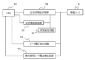
図2は、プロセスカートリッジを装着している状態の画像形成装置1の概略図である。3は回転可能な像担持体である感光ドラム、4は半導体レーザー5にて感光ドラム3上にレーザービームを走査し、静電潜像を形成する露光手段であるレーザースキャナである。2は交換可能なプロセスカートリッジである。プロセスカートリッジ2は、感光ドラム3上を一様に帯電するための帯電部材である帯電ローラ6と、感光ドラム3上にレーザースキャナ4によって形成された静電潜像を現像剤で現像する現像剤担持体7と、現像剤を格納する現像器8から構成される。10は感光ドラム3に現像された現像剤像を所定の記録材11に転写するための転写ローラ、12は記録材11に転写された現像剤を熱と圧にて定着するための定着器、13は定着器の温度を制御するための温度サーミスタである。14は記録材を給紙する給紙ローラである。15は記録材の搬送と同期をとるトップセンサ、16は定着後の記録材11を排紙トレイ17へ排出するための排紙ローラ、18は定着後の記録材11の有無を検出するための排紙センサである。19は、CPU20を備え、画像形成装置1を構成する各部を制御するエンジンコントローラである。21は画像形成
装置1の外部環境を検知する環境センサである。
<Outline of configuration and operation of image forming device and process cartridge>
FIG. 2 is a schematic view of the
また本実施例は、23°C50%RHの環境を使用し、解像度を600dpi、プロセススピード235mm/sec、露光量0.2μJ/cm2の条件で説明を行う。また、本実施例では負極性のトナーを使用したが、正極性のトナーを使用してもよい。この場合にはバイアス等の符号が全て逆となる以外の構成は負極性のトナーを使用する場合と同じである。 Further, this embodiment will be described using an environment of 23 ° C. 50% RH under the conditions of a resolution of 600 dpi, a process speed of 235 mm / sec, and an exposure amount of 0.2 μJ / cm2. Further, although the negative electrode toner is used in this embodiment, the positive electrode toner may be used. In this case, the configuration is the same as when the negative electrode toner is used, except that the signs such as bias are all reversed.
<帯電部の制御>
次に、本実施例での画像形成装置の帯電部の制御を行うブロック図を図3に示す。CPU20は、演算部30、記憶部31、交流電圧用駆動信号発生部32を有している。放電電流制御回路(バイアス印加手段)33内は、CPU20から信号を送られることで放電電流を制御しながら帯電ローラ6に電圧を印加している。ここでは、放電制御手段は、CPU20と放電電流制御回路33を含んで構成される。また、CPU20は、環境センサ21の出力値を検知し、出力値に応じた放電電流の制御を行っている。なお、放電電流制御回路33の詳細な動作については、以下で説明する。
<Control of charged part>
Next, FIG. 3 shows a block diagram for controlling the charged portion of the image forming apparatus in this embodiment. The
<放電電流制御>
本実施例における放電電流制御回路33を図4に示す。正弦波電圧印加部50で発生させた正弦波の交流高圧を、直流高圧回路51で出力される直流電圧に重畳させる。その振動電圧が帯電ローラ6に供給される。また、交流電流値検出手段としての交流電流検知部52の検知出力値に応じて、一定の振動電圧出力レベルとなるように交流電流値が制御されている。さらに放電電流制御回路33は、電圧振幅値検出部であるピーク電圧検出回路53と微分振幅値検出部である微分波形ピーク電圧検出回路54とを有する。これにより、CPU20は、出力する交流電圧のピーク値と微分波形ピーク値を検出することができる。ここでは、放電量検知手段は、ピーク電圧検出回路53、微分波形ピーク電圧検出回路54及びCPU20を含んで構成される。
<Discharge current control>
The discharge current control circuit 33 in this embodiment is shown in FIG. The AC high voltage of the sine wave generated by the sine wave
図5を用いて本実施例における放電電流の検出方法について説明する。図5は、帯電ローラ6に交流電圧を印加した際、帯電ローラ6に流れる帯電電流を示す。横軸は交流電圧のピーク電圧の値、縦軸は交流電流の実効値を示している。図5に示すように、帯電交流電圧が放電開始電圧(Vh)の2倍以下の領域では、帯電電流値の帯電交流電圧に対する関係式は原点を通るほぼ比例の直線で表される。この領域においては帯電ローラ6と感光ドラム3との間の抵抗性負荷および容量性負荷に応じた電流が流れる。これに対し、帯電交流電圧が放電開始電圧(Vh)の2倍以上の領域においては、帯電ローラ6と感光ドラム3との間に放電電流が発生し、この放電電流値が加算された帯電電流値Icが流れる。放電開始領域においては、放電する場合の特性を500で表し、放電しない場合の特性を501で表す。ここで特性500および特性501の関係から放電電流値を算出することができる。また、放電する場合のピーク値Va、放電しない場合のピーク値Va´、帯電電流Icの場合に、放電電流値Isは、以下の式(1)により求められる。
Is=Ic×(Va´−Va)/Va´ ……式(1)
つまり、(Va´−Va)/Va´を知ることができれば帯電電流に対する放電量が検知できる。図6を用いて(Va´−Va)/Va´の求め方を説明する。図6(A)に帯電ローラ6に印加されている帯電交流電圧出力波形、図6(B)に帯電交流電圧出力の微分波形を示している。帯電交流電圧の出力波形は、放電の影響を受けてピーク付近のレベルがΔV(=(Va´−Va))だけ下がった形状になる。また、微分電圧の波形については位相が90°遅れるため、ピーク値が放電の影響を受けることがない。そのため、微分電圧のピーク値(Vb)が、放電しない場合の出力電圧のピークレベル(Va´)に相当する。したがって、(Va´−Va)/Va´を求めることができる。図5、図6に示した方法によって放電電流値Isを検知し、放電電流値Isになるように帯電電流値Ic
を調整している。
A method of detecting the discharge current in this embodiment will be described with reference to FIG. FIG. 5 shows the charging current flowing through the charging
Is = Ic × (Va'-Va) / Va'... Equation (1)
That is, if (Va'-Va) / Va'can be known, the amount of discharge with respect to the charging current can be detected. A method of obtaining (Va'-Va) / Va'will be described with reference to FIG. FIG. 6A shows the charged AC voltage output waveform applied to the charging
Is being adjusted.
本実施例では、長手方向の放電ムラという課題を解決するために、上述した放電電流制御に加え、長手方向の一部分の放電情報(以下、部分放電情報)を検知し、それらの値から帯電バイアス出力値を補正することにより放電量の適正化を行った。また本実施例では部分放電情報として一部分の放電開始電圧(以下、部分放電開始電圧)を測定した。 In this embodiment, in order to solve the problem of uneven discharge in the longitudinal direction, in addition to the discharge current control described above, partial discharge information in the longitudinal direction (hereinafter referred to as partial discharge information) is detected, and the charge bias is obtained from those values. The amount of discharge was optimized by correcting the output value. Further, in this embodiment, a partial discharge start voltage (hereinafter referred to as a partial discharge start voltage) was measured as partial discharge information.
以下では、まず部分放電情報としての部分放電開始電圧を検知するために必要な放電開始電圧検知と、均一な帯電を行う方法を説明し、その後、部分放電情報としての部分放電開始電圧の検知方法を説明する。 In the following, first, the discharge start voltage detection required to detect the partial discharge start voltage as partial discharge information and the method of performing uniform charging will be described, and then the partial discharge start voltage detection method as partial discharge information will be described. Will be explained.
<放電開始電圧検知>
長手方向の部分放電情報を検知するため、本実施例では図7に示すようにDCバイアス放電開始電圧検知回路(放電情報検出手段)34を有する。DCバイアス放電開始電圧検知回路34は、CPU20から信号を送られることで帯電ローラ6にDC電圧を印加しながら放電開始電圧を検知する。図8に本発明におけるDCバイアス放電開始電圧検知回路34の概略構成を示す。100は電圧設定回路部でPWM信号に応じて、バイアス値が変えられる。101はトランス駆動回路部、102は高圧トランス部である。103はフィードバック回路部でR61を介して出力電圧をモニタし、PWM信号の設定に応じた出力電圧値になるように設けられた回路である。104は電流検出回路部(電流検知手段)で、帯電ローラ6に流れる電流値I62とフィードバック回路から流れる電流値I61を加算した電流値I63をR63で検出して、J110からアナログ値としてCPU20に伝送される。感光ドラム3と帯電ローラ6間で放電が開始するまでは、感光ドラム3と帯電ローラ6間は絶縁されている。そのため、放電が開始されるまでは、検出抵抗R63に流れる電流はフィードバック回路部103から流れてくるI61のみである。I61は、PWM信号で設定されるVpwmとVref、R64、R65で決められる。
I61=(Vref−Vpwm)/R64−Vpwm/R65
<Discharge start voltage detection>
In this embodiment, in order to detect partial discharge information in the longitudinal direction, a DC bias discharge start voltage detection circuit (discharge information detection means) 34 is provided as shown in FIG. The DC bias discharge start voltage detection circuit 34 detects the discharge start voltage while applying the DC voltage to the charging
I61 = (Vref-Vpwm) / R64-Vpwm / R65
また、その電流値I61がフィードバック抵抗R61を流れることで、出力電圧Voutも以下のように設定される。
Vout=I61×R61+Vpwm≒I61×R61
つまり、図9の直線(1)に示すように、放電が開始されるまでは、PWM信号に応じたI61の電流しか電流検出回路部のR63には流れないため、電流値は直線となる。
Further, when the current value I61 flows through the feedback resistor R61, the output voltage Vout is also set as follows.
Vout = I61 x R61 + Vpwm ≒ I61 x R61
That is, as shown in the straight line (1) of FIG. 9, until the discharge is started, only the current of I61 corresponding to the PWM signal flows to R63 of the current detection circuit unit, so that the current value becomes a straight line.
しかし、感光ドラム3と帯電ローラ6間で放電が開始されると、帯電ローラ6に流れる電流値I62とフィードバック回路から流れる電流値I61を加算したI63が、電流検出回路部のR63に流れる。つまり、電流値は、図9の曲線(2)に示すように放電が開始した時点で分岐点をもった曲線となる。このことより、帯電ローラ6に流れる電流は、曲線(2)から直線(1)を引いたIsdで算出することができる。
However, when the discharge is started between the
本実施例ではDCバイアスを操作しながら複数のIsdを計測し、あるIsdが所定の電流値になった時点をDCバイアス放電開始電圧と判断した。しかしながら、DCバイアス放電開始電圧を判断する方法はこれに限られない。例えば図10のように2つの異なるDCバイアスに対する放電量を測定し、そこから近似直線を引いて、この直線が放電量0となる点(図10のD)をDCバイアス放電開始電圧と判断するような方法でもよい。また精度の観点から測定点は2点に限らず増やしてもよい。 In this embodiment, a plurality of Isds are measured while operating the DC bias, and the time when a certain Isd reaches a predetermined current value is determined as the DC bias discharge start voltage. However, the method for determining the DC bias discharge start voltage is not limited to this. For example, as shown in FIG. 10, the discharge amount for two different DC biases is measured, an approximate straight line is drawn from the approximate straight line, and the point where this straight line becomes the discharge amount 0 (D in FIG. 10) is determined as the DC bias discharge start voltage. The method may be used. Further, from the viewpoint of accuracy, the number of measurement points is not limited to two and may be increased.
<長手方向に均一な帯電を行う方法>
次に、長手方向に均一な帯電を行う方法について説明する。長手方向の部分放電開始電圧を検知するためには、感光ドラム3を長手方向に均一に、すなわち一定電位に帯電する
必要がある。DCバイアス放電開始電圧は、帯電ローラ6の電位によって変化するため、長手方向で電位が均一でないとDCバイアス放電開始電圧から放電ムラを検知できない。長手方向に均一に帯電するには十分な帯電交流電圧を印加しなければならない。本実施例では現構成における帯電ACバイアスの最大値を印加している。また、その時に均一な帯電電位になっているかを確認する機構を持っていてもよい。
<Method of performing uniform charging in the longitudinal direction>
Next, a method of performing uniform charging in the longitudinal direction will be described. In order to detect the partial discharge start voltage in the longitudinal direction, it is necessary to charge the
以下に均一な帯電電位の確認機構について説明する。まず、所定のDCバイアスと最大のACバイアスを印加し、DCバイアス放電開始電圧検知回路34によりその時の長手方向全体のDCバイアス放電開始電圧Vdcth1(ave)を検知する。次に、ACバイアス(PWM)を1つステップダウンさせて同様に所定のDCバイアスとそのACバイアスを印加し、DCバイアス放電開始電圧検知回路34によりその時の長手方向全体のDCバイアス放電開始電圧Vdcth2(ave)を検知する。このとき、長手方向全体のDCバイアス放電開始電圧はそれぞれVdcth1(ave)=(1+C/Cd)Vpa+Vd1(ave),Vdcth2(ave)=(1+C/Cd)Vpa+Vd2(ave)と書ける。ここで、感光ドラム3の静電容量をCd、帯電ローラ6と感光ドラム3間の静電容量をCとしている。
The mechanism for confirming the uniform charging potential will be described below. First, a predetermined DC bias and the maximum AC bias are applied, and the DC bias discharge start voltage detection circuit 34 detects the DC bias discharge start voltage Vdcth1 (ave) in the entire longitudinal direction at that time. Next, the AC bias (PWM) is stepped down by one, and a predetermined DC bias and its AC bias are similarly applied, and the DC bias discharge start voltage detection circuit 34 at that time causes the DC bias discharge start voltage Vdcth2 in the entire longitudinal direction. (Ave) is detected. At this time, the DC bias discharge start voltage in the entire longitudinal direction can be written as Vdcth1 (ave) = (1 + C / Cd) Vpa + Vd1 (ave), Vdcth2 (ave) = (1 + C / Cd) Vpa + Vd2 (ave), respectively. Here, the capacitance of the
そして、Vdcth1(ave)−Vdcth2(ave)=Vd1(ave)−Vd2(ave)の関係式を得る。ここでVd1(ave)は最大のACバイアスで帯電された感光ドラム3の長手方向の平均の電位、Vd2(ave)は設定値が最大から一つステップダウンしたACバイアスで帯電された感光ドラム3の長手方向の平均の電位である。また、Vpaはパッシェン電圧であり、気圧と放電間距離の関数である。
Then, the relational expression of Vdcth1 (ave) -Vdcth2 (ave) = Vd1 (ave) -Vd2 (ave) is obtained. Here, Vd1 (ave) is the average potential in the longitudinal direction of the
図11には感光ドラム3の長手方向の電位とACバイアスとの関係を示している。Vac1、Vac2、Vac3はそれぞれ帯電ローラ6に印加するACバイアスのピーク間の値であり、Vac1<Vac2<Vac3である。ACバイアスによる帯電は、正放電と逆放電を繰り返すことで一定の帯電電位に安定させるが、ACバイアスが低いと、放電の長手方向ムラがある場合に帯電電位の長手方向ムラを引き起こす(図11の(a))。しかしACバイアスを上げていけば放電量が長手方向全体で上昇し、感光ドラム3の帯電電位は均一化される(図11の(b))。そしてそれに伴って平均電位は上昇していく。さらにACバイアスを上げて長手方向全体で帯電電位が均一になると平均電位は一定の値にとどまる(図11の(c))。
FIG. 11 shows the relationship between the electric potential of the
このことから、Vdcth1(ave)とVdcth2(ave)を比較することで、感光ドラム3の帯電電位の均一性を確認できる。具体的には、Vdcth1=Vdcth2ならばVd1=Vd2であり長手方向は均一化されていると判断できる。逆にVdcth1≠Vdcth2ならばVd1≠Vd2であり、十分に帯電できていないと判断する。この場合はどの電圧でも品質的に安定した画像が提供できないので、プロセスカートリッジとして寿命をユーザーに報知する等の対応をとる必要がある。
From this, the uniformity of the charging potential of the
なお、本実施例では帯電バイアスに最大のACバイアスを印加したが、この限りではなく、十分に均一に帯電できるバイアスを予め検討等により明確にして、その値を使用しても良い。 In this embodiment, the maximum AC bias is applied to the charging bias, but the present limitation is not limited to this, and the bias that can be charged sufficiently uniformly may be clarified in advance by examination or the like and the value may be used.
<部分放電情報の検知>
図12を用いて長手方向の部分放電情報としての部分放電開始電圧の検知について説明する。図12の横方向は長手方向の位置を表しており、縦方向は電位を表している。
<Detection of partial discharge information>
The detection of the partial discharge start voltage as the partial discharge information in the longitudinal direction will be described with reference to FIG. The horizontal direction of FIG. 12 represents the position in the longitudinal direction, and the vertical direction represents the potential.
まず図12(a)のように、上述通り最大のACバイアスを印加して感光ドラム3を均一に帯電(帯電電位:Vd)する。次に図12(b)のように感光ドラム3の印字可能領
域の一部に印字可能領域よりも長手方向の幅が小さい測定領域(以下、部分測定領域)D(i)を設定して、レーザースキャナ4により部分測定領域D(i)のみ露光し、露光電位(Vl)にする。長手方向で部分測定領域は複数箇所に設けてもよい。このとき、レーザースキャナ4によって露光された部分測定領域D(i)とこの部分測定領域を除く領域とが互いに異なる電位とされる。さらに、図12(c)のようにDCバイアス放電開始電圧検知回路34を用いて帯電ローラ6にDCバイアス(Vdc)を印加し、一部露光電位とした状態でDCバイアス放電開始電圧を測定する。この時、部分測定領域D(i)のみ放電し始めるので、部分測定領域D(i)のDCバイアス部分放電開始電圧Vdcth(i)が得られる。部分測定領域D(i)の感光ドラムの静電容量をCd(i)、帯電ローラ6と感光ドラム3間の静電容量をC(i)として等価回路を考える。そうすると、DCバイアス部分放電開始電圧の大きさはVdcth(i)=(1+C(i)/Cd(i))Vpa+|Vl|となる。
First, as shown in FIG. 12A, the
また、実際に画像を形成する時はDC+ACバイアスを印加するが、その時の部分測定領域D(i)のACバイアス部分放電開始電圧Vacth(i)は、Vacth(i)=2Vpa(1+C(i)/Cd(i))と書ける。ここでACバイアス部分放電開始電圧は、部分測定領域D(i)が帯電ローラ6から感光ドラム3へ放電を開始し始める電圧ではなく、感光ドラム3から帯電ローラ6へ逆放電もし始め、DCバイアスへ収束し始める電圧である。また、ACバイアス部分放電開始電圧はACバイアスのピーク間の値である。よって式(2)の関係式を満たす。
Vacth(i)=2(Vdcth(i)−|Vl|)……式(2)
長手方向全体のDCバイアス放電開始電圧をVdcth(ave)、長手方向全体のACバイアス放電開始電圧をVacth(ave)とすると、この関係式から式(3)を得ることができる。
Vacth(i)−Vacth(ave)=2(Vdcth(i)−Vdcth(ave))……式(3)
この式(3)により部分測定領域D(i)のACバイアス部分放電開始電圧を検知できる。実際は、このACバイアス部分放電開始電圧差Vacth(i)−Vacth(ave)を使用して補正を行う。ここで、Vdcth(ave)は、実際にDCバイアス放電開始電圧検知から長手方向全体のDCバイアス放電開始電圧を求めて使用している。しかしながらこの限りでなく、Vdcht(1),Vdcth(2)…Vdcht(N)の平均値を求めて使用しても良い。
Further, when an image is actually formed, a DC + AC bias is applied, and the AC bias partial discharge start voltage Vacts (i) in the partial measurement region D (i) at that time is Vacts (i) = 2Vpa (1 + C (i)). / Cd (i)) can be written. Here, the AC bias partial discharge start voltage is not the voltage at which the partial measurement region D (i) starts discharging from the charging
Vacts (i) = 2 (Vdcth (i)-| Vl |) ... Equation (2)
Assuming that the DC bias discharge start voltage in the entire longitudinal direction is Vdcth (ave) and the AC bias discharge start voltage in the entire longitudinal direction is Vact (ave), the equation (3) can be obtained from this relational expression.
Vacts (i) -Vacts (ave) = 2 (Vdcth (i) -Vdcth (ave)) ... Equation (3)
The AC bias partial discharge start voltage in the partial measurement region D (i) can be detected by this equation (3). Actually, the correction is performed using this AC bias partial discharge start voltage difference Vacts (i) -Vacts (ave). Here, Vdcth (ave) is actually used to obtain the DC bias discharge start voltage in the entire longitudinal direction from the detection of the DC bias discharge start voltage. However, the present invention is not limited to this, and the average value of Vdcht (1), Vdcth (2) ... Vdcht (N) may be obtained and used.
次に、部分放電開始電圧検知を行う部分測定領域について説明する。図13(a)に本実施例の部分測定領域を示す。図13の横方向は感光ドラム3の長手方向(回転方向に垂直な方向)を示す。本実施例では、感光ドラム3の面内の印字可能領域の長手方向を均一に7等分してそれぞれの領域で上記部分放電開始電圧検知を行った。しかしながら、部分測定領域の設定方法はこの限りでなく、等分でなくても良い。また、図13(b)のように紙のサイズに合わせて部分測定領域を決めてもよい。この場合は感光ドラム3の削れを考慮に入れて測定できるので、精度向上となる。さらには、紙の使用履歴をCPU20等に格納しておき、紙の使用履歴に応じて部分測定領域を変更等しても良い。
Next, the partial measurement area for detecting the partial discharge start voltage will be described. FIG. 13A shows a partial measurement area of this embodiment. The lateral direction of FIG. 13 indicates the longitudinal direction (direction perpendicular to the rotation direction) of the
また、感光ドラム3の削れの予測や帯電ローラ6の汚れの予測から予め放電開始電圧が大きくなる領域が分かっている場合などは、その領域のみ部分放電開始電圧を測定しても効果がある。この場合は、長手方向全体を対象とした放電開始電圧検知手段から全体のDCバイアス放電量開始電圧Vdcth(ave)を求めておく必要がある。
Further, when the region where the discharge start voltage becomes large is known in advance from the prediction of scraping of the
<補正方法>
次に、ACバイアス部分放電開始電圧から帯電バイアス出力値の補正を行う方法について説明する。
図14(a)は横軸が長手方向、縦軸が画像形成プロセス進行方向であり、感光ドラム3の部分測定領域を表している。本実施例では図14(a)のようにD(1)から順番に部分放電開始電圧を検知していった。しかし、方法はこの限りでなく、例えば測定する順番を変えたり、図15のように部分測定領域の検知に間隔があっても良い。図14(b)はそれぞれの部分測定領域におけるACバイアス部分放電開始電圧と長手全体のACバイアス放電開始電圧との差を示している。Vacth(i)−Vacth(ave)の最も大きい領域が最も放電しにくい部分であり、最も小さい領域が最も放電しやすい部分である。図14(b)に示す検知結果であれば、D(6)が最も放電しにくい部分であり、D(1)が最も放電しやすい部分である。以上で得られた部分測定領域におけるACバイアス部分放電開始電圧から補正を行う。
<Correction method>
Next, a method of correcting the charge bias output value from the AC bias partial discharge start voltage will be described.
In FIG. 14A, the horizontal axis is the longitudinal direction and the vertical axis is the image forming process progress direction, and represents a partial measurement region of the
図16に放電量とACバイアスの関係を示す。図16においては、感光ドラム3全体の放電量とACバイアスの関係が実線で示されている。そして、感光ドラム3の一番放電しやすい領域(図14(b)の例ではD(1))の放電量とACバイアスの関係が粗い破線で示されている。また、感光ドラム3の一番放電しにくい領域(図14(b)の例ではD(6))の放電量とACバイアスの関係が細かい破線で示されている。ACバイアスはピーク間の電圧値である。図16のように最も放電しにくい部分は放電特性が放電開始電圧差分シフトしてしまう。このため、全体の放電量が目標放電量に達していても、放電しにくい部分では放電量が目標放電量に達していない(図16のA)。図16(a)において縦軸の目標値を通り横軸に水平な破線と実線のグラフとの交点のACバイアスが、感光ドラム3の全体放電量が目標値となる場合のACバイアスを示す。上述の交点を通り縦軸に平行な破線と細かい破線との交点Aは、感光ドラム3全体の放電量が目標値となるような値のACバイアスを印加した際における、一番放電しにくい領域の放電量を示す。この場合の放電量は、図16(a)から分かるように目標値より少ない。このような場合、上記課題で述べたように砂地が発生してしまう場合がある。
FIG. 16 shows the relationship between the discharge amount and the AC bias. In FIG. 16, the relationship between the discharge amount of the entire
また、図16のように一番放電しやすい部分も、放電特性が放電開始電圧差分だけ流れやすい側にシフトしてしまう。そのため放電しやすい部分は過剰に放電量が流れてしまう。放電量が多いと感光ドラム3への局所的な削れ量が増えしまい、感光ドラム3に局所的なキズをつけてしまう場合がある。
Further, as shown in FIG. 16, even in the portion most easily discharged, the discharge characteristic shifts to the side where the discharge starting voltage difference is easy to flow. Therefore, the amount of discharge flows excessively in the portion that is easily discharged. If the amount of discharge is large, the amount of local scraping to the
露光による帯電電位から露光電位への変化は、露光による感光ドラム3でのキャリア(帯電が負帯電ならホール、正帯電なら電子)の生成と、そのキャリアによる表面電荷の中和によって起きる。しかし、露光電位は中和された表面電荷だけでなくドラムの静電容量にも依存する。簡単に式で書くと以下のようになる。
Vl=Vd+qd/ε……式(4)
ここでqは単位面積当たりのキャリアの電荷、dは感光ドラム3の膜厚、εは誘電率である。厳密にはqも膜厚に依存し式(4)はもう少し複雑になるが、関係自体は大きく変わらず、膜厚が少なくなると、VlはVdに近づく。つまり膜厚が少ないキズ部では、露光しても露光電位が十分に落ちない場合があり、ベタ黒等を印字するとキズ部は印字されず、画像に縦白スジが出てしまう場合があった。
The change from the charge potential to the exposure potential due to exposure occurs due to the generation of carriers (holes if the charge is negative, electrons if the charge is positive) on the
Vl = Vd + qd / ε …… Equation (4)
Here, q is the carrier charge per unit area, d is the film thickness of the
本実施例の補正方法は、感光ドラムの削れ量を抑えて画像に縦白スジが発生するのを抑制しながら、砂地を低減する補正方法である。 The correction method of this embodiment is a correction method of reducing sandy areas while suppressing the amount of scraping of the photosensitive drum and suppressing the occurrence of vertical white streaks in the image.
具体的方法としては、許容できる限界の削れ量を引き起こす放電量(I0)の時のACバイアス(V0)に対し、V0−(Vacth(ave)−Vacth(min))を削れ量許容閾値(Vth)として設定する。ここでVacth(min)は一番放電しやすい領域のACバイアス部分放電開始電圧である。I0は検討等によって予め求めておき、CPU20等に格納しておく。図16(a)では、放電量I0を通り、横軸に平行な一点
鎖線と、感光ドラム3全体の関係を示す実線との交点のACバイアスがV0である。そして、このV0に対して上述のように定められるVthは、図16(a)に示すように、一番放電しやすい領域の関係を示す粗い破線が、I0を通り横軸に平行な一点鎖線と交わる点のACバイアスである。このとき、Vthを通り縦軸に平行な破線と、一番放電しにくい領域の関係を示す細かい鎖線との交点がCである。すなわち、一番放電しやすい領域において許容できる限界の削れ量を引き起こす放電量(I0)となるようなACバイアスを設定した場合の、一番放電しにくい領域の関係をCで示している。放電量の目標値を通り横軸に平行な破線と一番放電しやすい領域の関係を示す粗い破線との交点BにおけるACバイアスの値は、一番放電しにくい領域の放電量が目標値となるようなACバイアスの値である。そして、図16(a)のように交点BのACバイアスが交点CのACバイアスより小さければ、交点Aから交点BまでACバイアスを補正する。つまり、全体が目標放電量に達するACバイアスに対して、交点BでのACバイアス値と交点AでのACバイアス値との差分であるVacth(max)−Vacth(ave)だけ加算する。ここでVacth(max)は一番放電しやすい領域のACバイアス部分放電開始電圧であり、Vacth(max)−Vacth(ave)は上述の式3から求められる。これにより一番放電しにくい部分も、目標とする放電量が流れる。また、交点BのACバイアスは交点CのACバイアスより小さいから、交点Aから交点BまでACバイアスを補正したとしても、一番放電しやすい領域においても許容できる限界の削れ量を超えることはない。
As a specific method, V0- (Vact (ave) -Vact (min)) is set to the scrap amount allowable threshold (Vth) with respect to the AC bias (V0) at the time of the discharge amount (I0) that causes the allowable limit of scraping amount. ). Here, Vact (min) is the AC bias partial discharge start voltage in the region where discharge is most likely to occur. I0 is obtained in advance by examination or the like and stored in the
図16(b)のように交点BのACバイアスが交点CのACバイアスより大きければ、ACバイアスをVthに設定し、これ以上放電量が上がらないように制御する。これは、図16(a)と同様に交点Aから交点BまでACバイアスを補正すると、交点BでのACバイアスが交点CでのACバイアスより大きいため、一番放電しやすい領域において許容できる限界の削れ量を引き起こす放電量(I0)を超えてしまうからである。これにより、一番放電しやすい部分も、許容できる限界の削れ量にとどめることができる。 If the AC bias at the intersection B is larger than the AC bias at the intersection C as shown in FIG. 16B, the AC bias is set to Vth and controlled so that the discharge amount does not increase any more. This is because when the AC bias is corrected from the intersection A to the intersection B as in FIG. 16A, the AC bias at the intersection B is larger than the AC bias at the intersection C, so that the limit is acceptable in the region where the discharge is most likely to occur. This is because the amount of discharge (I0) that causes the amount of scraping is exceeded. As a result, even the portion most easily discharged can be limited to the allowable limit of scraping amount.
この補正方法により、感光ドラムの削れ量を抑えて画像に縦白スジが発生するのを抑制しながら、砂地を抑制することができる。 By this correction method, it is possible to suppress the amount of scraping of the photosensitive drum, suppress the occurrence of vertical white streaks in the image, and suppress the sandy ground.
<効果の確認>
本実施例の効果を確認するために、上記補正方法と従来の放電電流制御方法である比較例において帯電不良の画像弊害を確認した。比較例の構成は、本実施例の構成に対し帯電バイアス出力値の補正を行わず、従来の放電電流制御を行う。その他は本実施例と同様なので説明は割愛する。測定は、4%印字率でキヤノン製CS680紙B5サイズを2枚間欠で30000枚通紙し、5000枚毎にキヤノン製CS680紙 A3サイズでベタ白画像1枚とベタ黒画像1枚を印刷した。通紙は感光ドラム3の中央部に紙が通るように行った。帯電不良の画像弊害としては、ベタ白画像に砂地の有無やそのレベルで確認した。感光ドラムの削れの画像弊害としては、ベタ黒に白スジ発生の有無やそのレベルで確認した。
<Confirmation of effect>
In order to confirm the effect of this example, the image adverse effect of poor charging was confirmed in the above correction method and the comparative example which is the conventional discharge current control method. In the configuration of the comparative example, the conventional discharge current control is performed without correcting the charge bias output value with respect to the configuration of the present embodiment. Others are the same as in this embodiment, so the explanation is omitted. The measurement was performed by passing 30,000 sheets of Canon CS680 paper B5 size intermittently at a 4% printing rate, and printing one solid white image and one solid black image on Canon CS680 paper A3 size every 5,000 sheets. .. The paper was passed so that the paper passed through the central portion of the
結果を表1に示す。表の砂地の部分の○は砂地発生なしを表している。△は砂地が発生しているが1cm2あたり5個以下、×は1cm2あたり5個より多く発生していることを表している。表の縦白スジの部分の○は縦白スジ発生なしを表している。△はスジがうっすら見える程度、×ははっきり見える程度を表している。結果を見ると、比較例では25000枚で砂地が△になっているのに対し、本実施例では発生が無いことが分かる。また、縦白スジは発生していないことも分かる。このことから本実施例は、感光ドラム3の削れ量を抑制しながら、砂地を抑制することができると分かった。

次に図1のフローチャートを用いて、本実施例における長手方向の部分放電情報の検出フローを含む画像形成方法について説明する。 Next, using the flowchart of FIG. 1, an image forming method including a detection flow of partial discharge information in the longitudinal direction in this embodiment will be described.
まず画像形成装置1にプリントコマンドが受信される(A101)と放電電流制御が開始され(A102)目標の放電量を出すための帯電バイアスが決定される。その後、部分放電情報を検知するかどうかを決定する(A103)。放電の長手方向ムラは感光ドラム3の長手方向削れムラや帯電ローラ6の汚れムラ等の経時変化によって起きるので、部分放電情報は常に測定する必要はない。本実施例の構成では、発生から顕在化まで1000枚程度かかることが分かっている。このため、本実施例では1000枚に1回部分放電情報の測定を行い、部分放電情報を検知しないと判断した場合は、CPU20に格納しておいた一番最近行ったデータを補正値として補正を行っている(A111)。しかしながらこれに限らず画像形成装置の構成に則した頻度で行えばよい。部分放電情報を検知すると判断した場合は、最初の測定領域の測定を開始する(A104)。まず、帯電ローラ6によって感光ドラム3を均一に帯電できるよう十分にバイアスを印加する(A105)。そして測定領域を露光し(A106)、DCバイアス放電開始電圧検知34によりDCバイアス放電開始電圧を検知する(A107)。測定が終了したら全ての領域を測定したか判断を行う(A108)。まだ測定領域全て測定していないと判断すれば、まだ測定していない領域を測定領域として(A109)A105に戻り、測定を開始する。測定領域全て測定したと判断すれば、測定値に基づいて放電電流制御の帯電バイアスを補正(A110)し、プリントを開始する(A112)。
First, when a print command is received by the image forming apparatus 1 (A101), discharge current control is started (A102), and a charging bias for producing a target discharge amount is determined. After that, it is determined whether or not to detect the partial discharge information (A103). Since the unevenness in the longitudinal direction of the discharge is caused by a change with time such as unevenness in the longitudinal direction of the
以上のようなフローを実施することにより、部分放電情報としての部分放電開始電圧を検知し、帯電バイアスを補正できる。 By carrying out the above flow, the partial discharge start voltage as the partial discharge information can be detected and the charging bias can be corrected.
なお、不揮発性メモリをプロセスカートリッジに設置して、目標放電電流値や使用状況
や使用環境等のバイアス電圧の決定に用いる情報等を、不揮発性メモリに記憶させても良い。プロセスカートリッジは画像形成装置本体から着脱可能であり、不揮発性メモリによってそれぞれのプロセスカートリッジに情報を持たせることができるので、それぞれのプロセスカートリッジに適切なバイアスを設定できる。
A non-volatile memory may be installed in the process cartridge, and information used for determining a target discharge current value, a usage status, a bias voltage such as a usage environment, and the like may be stored in the non-volatile memory. Since the process cartridge is removable from the image forming apparatus main body and information can be given to each process cartridge by the non-volatile memory, an appropriate bias can be set for each process cartridge.
なお、本実施例の構成はこれに限られたものではない。スピードや露光量等は本実施例を行うための一例にすぎない。また、本実施例では放電情報として放電開始電圧を検知し、部分放電情報として部分放電開始電圧を測定したが、この限りでなく、例えば放電情報として放電電流を検知して、一部分的な放電電流(以下、部分放電電流)を測定してもよい。放電電流の検知の場合、例えば一定の帯電電圧下での部分放電電流を検知することで長手方向の放電ムラを検知できる。 The configuration of this embodiment is not limited to this. The speed, exposure amount, etc. are only examples for carrying out this embodiment. Further, in this embodiment, the discharge start voltage is detected as the discharge information and the partial discharge start voltage is measured as the partial discharge information, but the present invention is not limited to this, for example, the discharge current is detected as the discharge information and a partial discharge current is detected. (Hereinafter, partial discharge current) may be measured. In the case of detecting the discharge current, for example, the discharge unevenness in the longitudinal direction can be detected by detecting the partial discharge current under a constant charging voltage.
実施例1は、感光ドラム3の削れ量を抑えて画像に縦白スジが発生するのを抑制しながら、砂地を抑制する補正方法であった。本実施例は、より高寿命な構成においても砂地を発生させることを抑制する補正方法であることを特徴とする。なお、実施例1と重複する部分については説明を割愛する。
The first embodiment was a correction method for suppressing sandy ground while suppressing the amount of scraping of the
図17に放電量とACバイアスの関係を示す。図17のように最も放電しにくい部分は放電特性が放電開始電圧差分シフトしてしまう。このため、全体の放電量が目標放電量に達していても、放電しにくい部分では放電量が目標放電量に達していない(図17のA)。このような場合、上記従来技術の課題で述べたように砂地が発生してしまうことがある。このような場合、実施例1の補正方法は有効であるが、高寿命化により印字枚数が多くなると、砂地の抑制は困難であることがあった。 FIG. 17 shows the relationship between the discharge amount and the AC bias. As shown in FIG. 17, the discharge characteristic shifts the discharge start voltage difference in the portion that is most difficult to discharge. Therefore, even if the total discharge amount reaches the target discharge amount, the discharge amount does not reach the target discharge amount in the portion where the discharge is difficult (A in FIG. 17). In such a case, sandy areas may be generated as described in the above-mentioned problems of the prior art. In such a case, the correction method of Example 1 is effective, but when the number of printed sheets increases due to the extension of the service life, it may be difficult to control the sandy area.
そこで、本実施例では閾値をなくして、砂地をなくすために図17のAからBまでACバイアスの補正を行った。つまり、ACバイアスを常にVacth(max)−Vacth(ave)だけ加算した。 Therefore, in this embodiment, the AC bias was corrected from A to B in FIG. 17 in order to eliminate the threshold value and eliminate the sandy area. That is, the AC bias was always added by Vacts (max) -Vacts (ave).
この補正方法により、長手方向で最も放電しにくい部分に目標の放電量が流れるので、砂地を抑制することができる。 By this correction method, since the target discharge amount flows to the portion where the discharge is most difficult in the longitudinal direction, sandy ground can be suppressed.
<効果の確認>
本実施例の効果を確認するために、実施例1と同様の効果確認を行った。確認対象は本実施例、実施例1、そして実施例1で用いた比較例の3つを対象とした。また、本実施例の効果は砂地の抑制であるので、砂地のみの確認を行った。測定に関しては実施例1と同様なので説明は割愛する。
<Confirmation of effect>
In order to confirm the effect of this example, the same effect confirmation as in Example 1 was performed. The confirmation targets were the present example, the first example, and the comparative example used in the first example. Moreover, since the effect of this example is the suppression of sandy areas, only sandy areas were confirmed. Since the measurement is the same as in Example 1, the description is omitted.
確認結果を表2に示す。結果をみると、本実施例では砂地の発生が無いことが分かる。このことから本実施例では、砂地を抑制することができると分かった。
なお、本実施例の構成はこれに限られたものではない。スピードや露光量等は本実施例を行うための一例にすぎない。また、本実施例では放電情報として放電開始電圧を検知し、部分放電情報として部分放電開始電圧を測定したが、この限りでなく、例えば放電情報として放電電流を検知して、部分放電電流を測定してもよい。 The configuration of this embodiment is not limited to this. The speed, exposure amount, etc. are only examples for carrying out this embodiment. Further, in this embodiment, the discharge start voltage is detected as the discharge information and the partial discharge start voltage is measured as the partial discharge information. However, the present invention is not limited to this, for example, the discharge current is detected as the discharge information and the partial discharge current is measured. You may.
実施例1、2は、部分放電情報検知の部分測定領域を露光部として部分放電情報を検知していた。本実施例は、部分放電情報検知の部分測定領域を、レーザースキャナ4によって露光しない非露光部とし、当該部分測定領域を除く非測定領域を、レーザースキャナ4によって露光する露光部とする。本実施例では、このようにして部分測定領域と部分測定領域を除く領域とが互いに異なる電位とされる。これにより、実施例1、2に対し部分放電情報の検知精度向上を行い、より高寿命な構成においても砂地の発生を抑制することを特徴としている。なお、実施例1、2と重複する部分については説明を割愛する。また、本実施例では部分放電情報として部分放電開始電圧を測定した。
In Examples 1 and 2, the partial discharge information was detected by using the partial measurement area for detecting the partial discharge information as an exposed portion. In this embodiment, the partial measurement area for detecting partial discharge information is a non-exposed area that is not exposed by the
実施例1ではDCバイアス部分放電開始電圧Vdcth(i)を求めるときに露光電位Vlの項が入っており、露光電位Vlが長手方向で大きく変化していないと考えていた。しかし、例えば感光ドラム3の膜厚が薄くなっていくと、帯電電位を長手方向に均一にしていても露光電位が感光ドラム3の膜厚によって大きく変化してしまう場合があった。図20に感光ドラム3の露光部と非露光部の電位の膜厚による変化を実線で示している。感光ドラム3の膜厚が薄くなってきたときに露光電位の膜厚依存性は大きくなっており、膜厚差による露光電位差は大きい。これは近年進んでいる画像形成装置の高寿命化により顕著になってきている。
In Example 1, when the DC bias partial discharge start voltage Vdcth (i) was obtained, the term of the exposure potential Vl was included, and it was considered that the exposure potential Vl did not change significantly in the longitudinal direction. However, for example, when the film thickness of the
このような場合には、露光電位Vlは測定領域において異なると考えられ(Vl=Vl(i))、式(2)から式(3)は求められず、式(5)のようになる。
Vacth(i)−Vacth(ave)=2(Vdcth(i)−Vdcth(ave))+2(|Vl(ave)|−|Vl(i)|)……式(5)
In such a case, the exposure potential Vl is considered to be different in the measurement region (Vl = Vl (i)), and the equations (2) to (3) are not obtained, and the equation (5) is obtained.
Vact (i) -Vact (ave) = 2 (Vdcth (i) -Vdcth (ave)) + 2 (| Vl (ave) |-| Vl (i) |) ... Equation (5)
つまり、式(5)の右辺第二項分の誤差が生じる。このような状態で式(3)を用いて補正すると、2(|Vl(ave)|−|Vl(i)|)だけ低く補正してしまうことになる場合がある。例えば、膜厚差によって放電ムラが生じている場合に、部分放電開始電圧が高い領域を検知しようとしても、部分放電開始電圧が高い領域は膜厚が厚い領域なの
で|Vl(ave)|>|Vl(i)|となる。すなわち、2(|Vl(ave)|−|Vl(i)|)(>0)分だけ低く補正されてしまい、十分なバイアスを印加できずに砂地が発生してしまうことがあった。
That is, an error corresponding to the second term on the right side of the equation (5) occurs. In such a state, if the correction is performed using the equation (3), the correction may be lowered by 2 (| Vl (ave) | − | Vl (i) |). For example, when discharge unevenness occurs due to a film thickness difference, even if an attempt is made to detect a region where the partial discharge start voltage is high, the region where the partial discharge start voltage is high is a region where the film thickness is thick. Vl (i) | That is, the correction is made lower by 2 (| Vl (ave) |-| Vl (i) |) (> 0), and a sufficient bias may not be applied and sandy areas may be generated.
そこで、本実施例では部分測定領域を非露光部とすることで露光電位の影響を回避している。そのため精度よく部分放電開始電圧を検知できる。以下、図19を用いて本実施例における長手方向の部分放電開始電圧の検知について詳細に説明する。図19の横方向は長手方向の位置を示しており、縦方向は電位を表している。 Therefore, in this embodiment, the influence of the exposure potential is avoided by setting the partial measurement region as the non-exposed portion. Therefore, the partial discharge start voltage can be detected with high accuracy. Hereinafter, the detection of the partial discharge start voltage in the longitudinal direction in this embodiment will be described in detail with reference to FIG. The horizontal direction of FIG. 19 indicates the position in the longitudinal direction, and the vertical direction indicates the electric potential.
まず、図19(a)のように感光ドラム3を均一に帯電(帯電電位:Vd)する。次に、図19(b)のようにレーザースキャナ4により部分測定領域D(i)以外の領域を露光し、露光電位(Vl)にする。さらに、図19(c)のようにDCバイアス放電開始電圧検知回路34を用いて帯電ローラ6にDCバイアス(Vdc)を印加し、部分測定領域D(i)のみ放電する領域でDCバイアス放電開始電圧を測定する。その結果、部分測定領域D(i)のDCバイアス部分放電開始電圧Vdcth(i)が得られる。部分測定領域D(i)の感光ドラム3の静電容量をCd(i)、帯電ローラ6と感光ドラム3間の静電容量をC(i)とすると、DCバイアス放電開始電圧は、Vdcth(i)=(1+C(i)/Cd(i))Vpa+Vdとなる。ここで、Vpaはパッシェン電圧であり、気圧と放電間距離の関数である。図20に破線で示すように、帯電電位はACバイアスにより膜厚に関係なく均一に帯電されるので、膜厚に大きく依存しない。よって、実施例1と同様に式(3)を得ることができる。
Vacth(i)−Vacth(ave)=2(Vdcth(i)−Vdcth(ave))……式(3)
つまり、本実施例では測定する領域を非露光部とすることにより、露光電位変化の影響を回避している。そのため、精度よく部分放電開始電圧を検知できる。
First, as shown in FIG. 19A, the
Vacts (i) -Vacts (ave) = 2 (Vdcth (i) -Vdcth (ave)) ... Equation (3)
That is, in this embodiment, the influence of the change in the exposure potential is avoided by setting the area to be measured as the non-exposed area. Therefore, the partial discharge start voltage can be detected with high accuracy.
<効果の確認>
本実施例の効果を確認するために、実施例2と同様の効果確認を行った。確認対象としては本実施例、実施例1、実施例2及び実施例1で用いた比較例の4つを対象とした。測定に関しては実施例1、2と同様のため説明を割愛する。確認結果を表3に示す。結果を見ると、本実施例では実施例1、2にくらべて砂地の発生をより抑制できているのが分かる。
<Confirmation of effect>
In order to confirm the effect of this example, the same effect confirmation as in Example 2 was performed. Four confirmation targets were used in this example, Example 1, Example 2, and Comparative Example used in Example 1. Since the measurement is the same as in Examples 1 and 2, the description thereof will be omitted. The confirmation results are shown in Table 3. Looking at the results, it can be seen that in this example, the occurrence of sandy ground can be further suppressed as compared with Examples 1 and 2.
これは、実施例1、2においては通紙枚数後半で、上述したように膜厚による露光電位依存性による測定誤差によって十分なバイアス補正ができなかったためと考えられる。それに対し、本実施例では適正に補正できているのが分かる。
なお、本実施例の構成はこれに限られたものではない。スピードや露光量、感光ドラム膜厚等は本実施例を行うための一例にすぎない。また、本実施例では放電情報として放電開始電圧を検知し、部分放電情報として部分放電開始電圧を測定したが、この限りでなく、例えば放電情報として放電電流を検知して、部分放電電流を測定してもよい。 The configuration of this embodiment is not limited to this. The speed, exposure amount, photosensitive drum film thickness, etc. are only examples for performing this embodiment. Further, in this embodiment, the discharge start voltage is detected as the discharge information and the partial discharge start voltage is measured as the partial discharge information. However, the present invention is not limited to this, for example, the discharge current is detected as the discharge information and the partial discharge current is measured. You may.
実施例1から3は、部分放電情報検知としての部分放電開始電圧検知にDCバイアス放電開始電圧検知回路34を使用していた。本実施例では、部分放電開始電圧検知に放電電流制御回路33を使用しても実施例1と同様の効果が得られる構成を説明する。すなわち、本実施例では、放電電流制御回路33が放電情報検知手段を構成する。なお、実施例1と重複する部分については同様の符号を用いて説明を割愛する。本実施例では部分放電情報として部分放電開始電圧を測定した。 In Examples 1 to 3, the DC bias discharge start voltage detection circuit 34 was used for the partial discharge start voltage detection as the partial discharge information detection. In this embodiment, a configuration will be described in which the same effect as that of the first embodiment can be obtained even if the discharge current control circuit 33 is used for detecting the partial discharge start voltage. That is, in this embodiment, the discharge current control circuit 33 constitutes the discharge information detecting means. The same reference numerals are used for the parts that overlap with those of the first embodiment, and the description thereof will be omitted. In this example, the partial discharge start voltage was measured as the partial discharge information.
図21を用いて長手方向の部分放電開始電圧の検知について説明する。図21は、横軸は長手方向の位置を表しており、縦軸は電位を表している。 The detection of the partial discharge start voltage in the longitudinal direction will be described with reference to FIG. In FIG. 21, the horizontal axis represents the position in the longitudinal direction, and the vertical axis represents the electric potential.
まず、図21(a)のように感光ドラム3を均一に帯電(帯電電位:Vd)する。次に,図21(b)のようにレーザースキャナ4により部分測定領域D(i)のみ露光し、露光電位(Vl)にする。そして、図21(c)のように放電電流制御回路33を用いて帯電ローラ6にDC+ACバイアスを印加する。このときバイアスが図21(c)のように片側のピークが固定され(Vt)もう片側に増幅するようにする。具体的には、DCバイアスをVt+Vac/2となるように設定し、ACバイアスと連動するようにする。ここで、Vtは放電開始しない領域のバイアスに設定される。例えば、Vdやその近傍の値等に設定すればよい。図22に、印加するAC帯電バイアスの時間変化を示す。図22のように片側に徐々に増幅するようにして、部分測定領域D(i)のみ放電する状態で放電開始電圧を測定する。その結果、部分測定領域D(i)が放電を開始し、部分測定領域D(i)の放電開始電圧Vacth´(i)が得られる。
First, as shown in FIG. 21A, the
放電開始電圧Vacth´(i)の大きさは、
Vacth´(i)=(1+C(i)/Cd(i))Vpa+|Vl|−|Vt|となる。
The magnitude of the discharge start voltage Voltage'(i) is
Vact'(i) = (1 + C (i) / Cd (i)) Vpa + | Vl |-| Vt |.
また、ACバイアス放電開始電圧Vacth(i)は実施例1と同様に、Vacth(i)=2Vpa(1+C(i)/Cd(i))と書ける。よって、Vacth(i)=2(Vacth´(i)−|Vl|+|Vt|)……式(6)の関係式を満たす。 Further, the AC bias discharge start voltage Vacts (i) can be written as Vacts (i) = 2Vpa (1 + C (i) / Cd (i)) as in the first embodiment. Therefore, Vacts (i) = 2 (Vacts'(i)-| Vl | + | Vt |) ... Satisfies the relational expression of the equation (6).
放電開始電圧Vacth´(i)の平均をVacth´(ave)、ACバイアス放電開始電圧の平均をVacth(ave)とすると、この関係式から式(7)を得ることができる。
Vacth(i)−Vacth(ave)=2(Vacth´(i)−Vacth´(ave))……式(7)
Assuming that the average of the discharge start voltage Vacts'(i) is Vacts' (ave) and the average of the AC bias discharge start voltages is Vacts (ave), the equation (7) can be obtained from this relational expression.
Vacts (i) -Vacts (ave) = 2 (Vacts'(i) -Vacts' (ave)) ... Equation (7)
この式(7)により、測定領域D(i)のACバイアス放電開始電圧を検知できる。なお、本実施例では、部分測定領域を露光部としたが、実施例3のように非露光部としてもよい。 From this equation (7), the AC bias discharge start voltage in the measurement region D (i) can be detected. In this embodiment, the partially measured region is the exposed portion, but it may be the non-exposed portion as in the third embodiment.
本実施例について実施例1と同様の効果確認を行ったところ、実施例1の表1と同様の結果が得られた。このことから、本実施例から部分放電開始電圧検知に放電電流制御回路33を使用しても実施例1と同様の効果が得られることがわかった。 When the same effect as in Example 1 was confirmed for this example, the same result as in Table 1 of Example 1 was obtained. From this, it was found from this example that the same effect as in Example 1 can be obtained even if the discharge current control circuit 33 is used for detecting the partial discharge start voltage.
なお、本実施例の構成はこれに限られたものではない。スピードや露光量、等は本実施例を行うための一例にすぎない。また、本実施例では放電情報として放電開始電圧を検知し、部分放電情報として部分放電開始電圧を測定したが、この限りでなく、例えば放電情報として放電電流を検知して、部分放電電流を測定してもよい。 The configuration of this embodiment is not limited to this. The speed, exposure amount, etc. are only examples for carrying out this embodiment. Further, in this embodiment, the discharge start voltage is detected as the discharge information and the partial discharge start voltage is measured as the partial discharge information. However, the present invention is not limited to this, for example, the discharge current is detected as the discharge information and the partial discharge current is measured. You may.
1:画像形成装置、3:感光ドラム、4:レーザースキャナ、6:帯電ローラ、19:エンジンコントローラ、20:CPU、33:放電電流制御回路、34:DCバイアス放電開始電圧検知回路 1: Image forming device, 3: Photosensitive drum, 4: Laser scanner, 6: Charging roller, 19: Engine controller, 20: CPU, 33: Discharge current control circuit, 34: DC bias discharge start voltage detection circuit
Claims (10)
前記像担持体を露光する露光手段と、
前記像担持体を帯電する帯電部材と、
前記帯電部材にバイアス電圧を印加するバイアス印加手段と、
前記帯電部材と前記像担持体との間で放電する電流量を検知する放電量検知手段と、前記放電量検知手段によって検知される放電電流量から前記帯電部材に印加するバイアス電圧を決定する放電電流制御手段と、
前記帯電部材と前記像担持体との間の放電に関する情報である放電情報を検出する放電情報検出手段とを有し、
前記放電情報検出手段は、前記像担持体の面内の印字可能な領域の一部に回転方向に対し垂直な方向の幅が前記印字可能な領域の幅よりも小さい領域を部分測定領域と設定し、前記帯電部材により前記像担持体を一定の電位に帯電した後に前記露光手段によって前記部分測定領域と前記部分測定領域を除く領域とで互いに異なる電位を形成している時に前記部分測定領域と前記帯電部材との間の放電に関する部分放電情報を検出し、
前記放電電流制御手段は、該部分放電情報に基づいて前記帯電部材に印加される画像形成におけるバイアス電圧を補正することを特徴とする画像形成装置。 A rotatable image carrier that carries a latent image and
An exposure means for exposing the image carrier and
A charging member that charges the image carrier and
Bias application means for applying a bias voltage to the charging member, and
A discharge amount detecting means for detecting the amount of current discharged between the charging member and the image carrier, and a discharge for determining a bias voltage applied to the charging member from the amount of discharge current detected by the discharge amount detecting means. Current control means and
It has a discharge information detecting means for detecting discharge information which is information about discharge between the charging member and the image carrier.
The discharge information detecting means sets a part of the in-plane printable area of the image carrier whose width in the direction perpendicular to the rotation direction is smaller than the width of the printable area as a partial measurement area. Then, when the image carrier is charged to a constant potential by the charging member and then different potentials are formed between the partial measurement region and the region other than the partial measurement region by the exposure means, the partial measurement region and the partial measurement region are formed. The partial discharge information regarding the discharge with the charging member is detected, and the discharge information is detected.
The discharge current control means is an image forming apparatus that corrects a bias voltage in image forming applied to the charging member based on the partial discharge information.
領域と前記部分測定領域を除く領域とが互いに異なる電位にされることにより、前記部分放電情報を検出することを特徴とする請求項1ないし3のいずれか1項に記載の画像形成装置。 The partial measurement area and the partial measurement area are divided by using the partial measurement area as a non-exposed area that is not exposed by the exposure means and the area excluding the partial measurement area as an exposed area that is exposed by the exposure means. The image forming apparatus according to any one of claims 1 to 3, wherein the partial discharge information is detected by setting the regions to be excluded to different potentials.
前記像担持体を露光する露光手段と、
前記像担持体を帯電する帯電部材と、
前記帯電部材にバイアス電圧を印加するバイアス印加手段と、
前記帯電部材と前記像担持体との間で放電する電流量を検知する放電量検知手段と、
前記放電量検知手段で得られる放電電流量から前記帯電部材に印加するバイアス電圧を決定する放電電流制御手段と、
を有している画像形成装置における画像形成方法であって、
前記像担持体の面内の印字可能な領域の一部に回転方向に対し垂直な方向の幅が前記印字可能な領域よりも小さく設定された部分測定領域に対して、前記帯電部材により前記像担持体を一定の電位に帯電する工程と、
前記露光手段により前記部分測定領域と前記部分測定領域を除く領域とを互いに異なる電位とする工程と、
前記部分測定領域と前記帯電部材との間の放電に関する部分放電情報を検出する工程と、
前記部分放電情報に基づいて前記帯電部材に印加される画像形成におけるバイアス電圧を補正する工程を有することを特徴とする画像形成方法。 A rotatable image carrier that carries a latent image and
An exposure means for exposing the image carrier and
A charging member that charges the image carrier and
Bias application means for applying a bias voltage to the charging member, and
Discharge amount detecting means for detecting the amount of current discharged between the charging member and the image carrier, and
Discharge current control means for determining the bias voltage applied to the charging member from the amount of discharge current obtained by the discharge amount detecting means, and
It is an image forming method in an image forming apparatus which has.
The image is provided by the charging member with respect to a partial measurement region in which the width in the direction perpendicular to the rotation direction is set to be smaller than the printable region in a part of the printable region in the plane of the image carrier. The process of charging the carrier to a constant potential and
A step of setting the partial measurement region and the region excluding the partial measurement region to different potentials by the exposure means, and
A step of detecting partial discharge information regarding a discharge between the partial measurement region and the charging member, and
An image forming method comprising a step of correcting a bias voltage in image forming applied to the charging member based on the partial discharge information.
Priority Applications (1)
| Application Number | Priority Date | Filing Date | Title |
|---|---|---|---|
| US15/605,190 US10146150B2 (en) | 2016-06-01 | 2017-05-25 | Process cartridge, image forming apparatus, image forming method |
Applications Claiming Priority (2)
| Application Number | Priority Date | Filing Date | Title |
|---|---|---|---|
| JP2016110417 | 2016-06-01 | ||
| JP2016110417 | 2016-06-01 |
Publications (3)
| Publication Number | Publication Date |
|---|---|
| JP2017219832A JP2017219832A (en) | 2017-12-14 |
| JP2017219832A5 JP2017219832A5 (en) | 2020-06-18 |
| JP6921611B2 true JP6921611B2 (en) | 2021-08-18 |
Family
ID=60656203
Family Applications (1)
| Application Number | Title | Priority Date | Filing Date |
|---|---|---|---|
| JP2017091436A Active JP6921611B2 (en) | 2016-06-01 | 2017-05-01 | Process cartridge, image forming device, image forming method |
Country Status (1)
| Country | Link |
|---|---|
| JP (1) | JP6921611B2 (en) |
Families Citing this family (2)
| Publication number | Priority date | Publication date | Assignee | Title |
|---|---|---|---|---|
| JP7124380B2 (en) | 2018-03-29 | 2022-08-24 | ブラザー工業株式会社 | image forming device |
| KR20200109996A (en) | 2019-03-15 | 2020-09-23 | 휴렛-팩커드 디벨롭먼트 컴퍼니, 엘.피. | Detecting occurrence of background in non-image area |
Family Cites Families (6)
| Publication number | Priority date | Publication date | Assignee | Title |
|---|---|---|---|---|
| JP2004301908A (en) * | 2003-03-28 | 2004-10-28 | Canon Inc | Image forming apparatus |
| JP4994650B2 (en) * | 2005-12-02 | 2012-08-08 | キヤノン株式会社 | Charging device |
| JP4926571B2 (en) * | 2006-06-30 | 2012-05-09 | キヤノン株式会社 | Image forming apparatus |
| US8483585B2 (en) * | 2008-09-29 | 2013-07-09 | Lexmark International, Inc. | System and method for adjusting voltage bias of a charge roller of an image forming device based on environmental conditions to control white vector |
| JP2012133052A (en) * | 2010-12-20 | 2012-07-12 | Canon Inc | Image forming apparatus |
| JP2012163864A (en) * | 2011-02-08 | 2012-08-30 | Canon Inc | Image forming apparatus |
-
2017
- 2017-05-01 JP JP2017091436A patent/JP6921611B2/en active Active
Also Published As
| Publication number | Publication date |
|---|---|
| JP2017219832A (en) | 2017-12-14 |
Similar Documents
| Publication | Publication Date | Title |
|---|---|---|
| US7471906B2 (en) | Image forming apparatus and image forming method | |
| JP5512009B2 (en) | Image forming apparatus | |
| JP5197264B2 (en) | Image forming apparatus | |
| JP2009053681A (en) | Image forming apparatus and method of controlling the same | |
| US10001719B2 (en) | Image forming apparatus | |
| JP6921611B2 (en) | Process cartridge, image forming device, image forming method | |
| US10146150B2 (en) | Process cartridge, image forming apparatus, image forming method | |
| JP6590578B2 (en) | Image forming apparatus | |
| US20170364010A1 (en) | Image forming apparatus | |
| JP6642997B2 (en) | Image forming device | |
| JP5690109B2 (en) | Voltage control method for image forming apparatus, recording medium therefor, voltage control apparatus, and image forming apparatus having voltage control apparatus | |
| JP2011133686A (en) | Image forming apparatus | |
| US8099011B2 (en) | Image forming apparatus | |
| JP5106034B2 (en) | Image forming apparatus | |
| JP2007327992A (en) | Image forming apparatus | |
| US9727000B2 (en) | Determining surface potential of image bearing member of image forming apparatus | |
| JP2018004917A (en) | Image forming apparatus | |
| JP4266787B2 (en) | Charging voltage control circuit and image forming apparatus | |
| JP6478720B2 (en) | Image forming apparatus | |
| JP2005128150A (en) | Service life detecting device for image carrier and image forming apparatus | |
| JP2009205110A (en) | Image forming apparatus | |
| JP2020160365A (en) | Image formation apparatus | |
| JP6700997B2 (en) | Image forming apparatus and image forming method | |
| JP7124597B2 (en) | image forming device | |
| US10520859B2 (en) | Image forming apparatus controlling surface potential of image bearing member |
Legal Events
| Date | Code | Title | Description |
|---|---|---|---|
| RD02 | Notification of acceptance of power of attorney |
Free format text: JAPANESE INTERMEDIATE CODE: A7422 Effective date: 20181116 |
|
| A621 | Written request for application examination |
Free format text: JAPANESE INTERMEDIATE CODE: A621 Effective date: 20200430 |
|
| A521 | Written amendment |
Free format text: JAPANESE INTERMEDIATE CODE: A523 Effective date: 20200507 |
|
| A977 | Report on retrieval |
Free format text: JAPANESE INTERMEDIATE CODE: A971007 Effective date: 20210226 |
|
| A131 | Notification of reasons for refusal |
Free format text: JAPANESE INTERMEDIATE CODE: A131 Effective date: 20210302 |
|
| A521 | Written amendment |
Free format text: JAPANESE INTERMEDIATE CODE: A523 Effective date: 20210427 |
|
| TRDD | Decision of grant or rejection written | ||
| A01 | Written decision to grant a patent or to grant a registration (utility model) |
Free format text: JAPANESE INTERMEDIATE CODE: A01 Effective date: 20210629 |
|
| A61 | First payment of annual fees (during grant procedure) |
Free format text: JAPANESE INTERMEDIATE CODE: A61 Effective date: 20210728 |
|
| R151 | Written notification of patent or utility model registration |
Ref document number: 6921611 Country of ref document: JP Free format text: JAPANESE INTERMEDIATE CODE: R151 |