JP6904769B2 - Display device - Google Patents
Display device Download PDFInfo
- Publication number
- JP6904769B2 JP6904769B2 JP2017083615A JP2017083615A JP6904769B2 JP 6904769 B2 JP6904769 B2 JP 6904769B2 JP 2017083615 A JP2017083615 A JP 2017083615A JP 2017083615 A JP2017083615 A JP 2017083615A JP 6904769 B2 JP6904769 B2 JP 6904769B2
- Authority
- JP
- Japan
- Prior art keywords
- transistor
- layer
- insulating layer
- semiconductor layer
- electrode
- Prior art date
- Legal status (The legal status is an assumption and is not a legal conclusion. Google has not performed a legal analysis and makes no representation as to the accuracy of the status listed.)
- Active
Links
- 239000004065 semiconductor Substances 0.000 claims description 339
- 239000004973 liquid crystal related substance Substances 0.000 claims description 78
- QVGXLLKOCUKJST-UHFFFAOYSA-N atomic oxygen Chemical compound [O] QVGXLLKOCUKJST-UHFFFAOYSA-N 0.000 claims description 66
- 229910052760 oxygen Inorganic materials 0.000 claims description 66
- 239000001301 oxygen Substances 0.000 claims description 66
- 239000011701 zinc Substances 0.000 claims description 45
- 229920005989 resin Polymers 0.000 claims description 31
- 239000011347 resin Substances 0.000 claims description 31
- 229910052751 metal Inorganic materials 0.000 claims description 28
- 239000002184 metal Substances 0.000 claims description 26
- 229910052738 indium Inorganic materials 0.000 claims description 18
- APFVFJFRJDLVQX-UHFFFAOYSA-N indium atom Chemical compound [In] APFVFJFRJDLVQX-UHFFFAOYSA-N 0.000 claims description 14
- 229910052725 zinc Inorganic materials 0.000 claims description 14
- HCHKCACWOHOZIP-UHFFFAOYSA-N Zinc Chemical compound [Zn] HCHKCACWOHOZIP-UHFFFAOYSA-N 0.000 claims description 10
- 229910052733 gallium Inorganic materials 0.000 claims description 10
- GYHNNYVSQQEPJS-UHFFFAOYSA-N Gallium Chemical compound [Ga] GYHNNYVSQQEPJS-UHFFFAOYSA-N 0.000 claims description 6
- 239000010410 layer Substances 0.000 description 907
- 230000006870 function Effects 0.000 description 138
- 238000000034 method Methods 0.000 description 100
- 239000000463 material Substances 0.000 description 89
- 239000010408 film Substances 0.000 description 69
- 239000000758 substrate Substances 0.000 description 68
- 229910044991 metal oxide Inorganic materials 0.000 description 44
- 230000001965 increasing effect Effects 0.000 description 43
- 150000004706 metal oxides Chemical class 0.000 description 33
- 239000012535 impurity Substances 0.000 description 32
- MWUXSHHQAYIFBG-UHFFFAOYSA-N nitrogen oxide Inorganic materials O=[N] MWUXSHHQAYIFBG-UHFFFAOYSA-N 0.000 description 32
- 239000013078 crystal Substances 0.000 description 31
- IJGRMHOSHXDMSA-UHFFFAOYSA-N Atomic nitrogen Chemical compound N#N IJGRMHOSHXDMSA-UHFFFAOYSA-N 0.000 description 28
- 230000005684 electric field Effects 0.000 description 21
- 230000005669 field effect Effects 0.000 description 21
- 239000010936 titanium Substances 0.000 description 19
- 238000005338 heat storage Methods 0.000 description 18
- RTAQQCXQSZGOHL-UHFFFAOYSA-N Titanium Chemical compound [Ti] RTAQQCXQSZGOHL-UHFFFAOYSA-N 0.000 description 16
- 229910052782 aluminium Inorganic materials 0.000 description 16
- XAGFODPZIPBFFR-UHFFFAOYSA-N aluminium Chemical compound [Al] XAGFODPZIPBFFR-UHFFFAOYSA-N 0.000 description 16
- 229910052719 titanium Inorganic materials 0.000 description 16
- OKTJSMMVPCPJKN-UHFFFAOYSA-N Carbon Chemical compound [C] OKTJSMMVPCPJKN-UHFFFAOYSA-N 0.000 description 15
- 239000004020 conductor Substances 0.000 description 15
- 230000001976 improved effect Effects 0.000 description 15
- 238000004519 manufacturing process Methods 0.000 description 14
- 239000000203 mixture Substances 0.000 description 14
- 229910052757 nitrogen Inorganic materials 0.000 description 14
- 229910052581 Si3N4 Inorganic materials 0.000 description 13
- 230000015572 biosynthetic process Effects 0.000 description 13
- 239000001257 hydrogen Substances 0.000 description 13
- 229910052739 hydrogen Inorganic materials 0.000 description 13
- HQVNEWCFYHHQES-UHFFFAOYSA-N silicon nitride Chemical compound N12[Si]34N5[Si]62N3[Si]51N64 HQVNEWCFYHHQES-UHFFFAOYSA-N 0.000 description 13
- 206010021143 Hypoxia Diseases 0.000 description 12
- XUIMIQQOPSSXEZ-UHFFFAOYSA-N Silicon Chemical compound [Si] XUIMIQQOPSSXEZ-UHFFFAOYSA-N 0.000 description 12
- 229910021417 amorphous silicon Inorganic materials 0.000 description 12
- 238000004364 calculation method Methods 0.000 description 12
- 238000005530 etching Methods 0.000 description 12
- 229910052710 silicon Inorganic materials 0.000 description 12
- 239000010703 silicon Substances 0.000 description 12
- PXHVJJICTQNCMI-UHFFFAOYSA-N Nickel Chemical compound [Ni] PXHVJJICTQNCMI-UHFFFAOYSA-N 0.000 description 11
- 238000005229 chemical vapour deposition Methods 0.000 description 11
- 238000009413 insulation Methods 0.000 description 11
- QGZKDVFQNNGYKY-UHFFFAOYSA-N Ammonia Chemical compound N QGZKDVFQNNGYKY-UHFFFAOYSA-N 0.000 description 10
- -1 aluminum nitride nitride Chemical class 0.000 description 10
- PMHQVHHXPFUNSP-UHFFFAOYSA-M copper(1+);methylsulfanylmethane;bromide Chemical compound Br[Cu].CSC PMHQVHHXPFUNSP-UHFFFAOYSA-M 0.000 description 10
- TWNQGVIAIRXVLR-UHFFFAOYSA-N oxo(oxoalumanyloxy)alumane Chemical compound O=[Al]O[Al]=O TWNQGVIAIRXVLR-UHFFFAOYSA-N 0.000 description 10
- 125000004429 atom Chemical group 0.000 description 9
- 238000000231 atomic layer deposition Methods 0.000 description 9
- 239000010949 copper Substances 0.000 description 9
- 230000007547 defect Effects 0.000 description 9
- 150000004767 nitrides Chemical class 0.000 description 9
- 239000000126 substance Substances 0.000 description 9
- UFHFLCQGNIYNRP-UHFFFAOYSA-N Hydrogen Chemical compound [H][H] UFHFLCQGNIYNRP-UHFFFAOYSA-N 0.000 description 8
- 230000005685 electric field effect Effects 0.000 description 8
- 239000007789 gas Substances 0.000 description 8
- 238000010438 heat treatment Methods 0.000 description 8
- 238000012986 modification Methods 0.000 description 8
- 230000004048 modification Effects 0.000 description 8
- 229910052750 molybdenum Inorganic materials 0.000 description 8
- 229910052814 silicon oxide Inorganic materials 0.000 description 8
- RYGMFSIKBFXOCR-UHFFFAOYSA-N Copper Chemical compound [Cu] RYGMFSIKBFXOCR-UHFFFAOYSA-N 0.000 description 7
- ZOKXTWBITQBERF-UHFFFAOYSA-N Molybdenum Chemical compound [Mo] ZOKXTWBITQBERF-UHFFFAOYSA-N 0.000 description 7
- VYPSYNLAJGMNEJ-UHFFFAOYSA-N Silicium dioxide Chemical compound O=[Si]=O VYPSYNLAJGMNEJ-UHFFFAOYSA-N 0.000 description 7
- 230000008859 change Effects 0.000 description 7
- 229910052802 copper Inorganic materials 0.000 description 7
- 239000002178 crystalline material Substances 0.000 description 7
- 238000009792 diffusion process Methods 0.000 description 7
- 239000011521 glass Substances 0.000 description 7
- 239000011810 insulating material Substances 0.000 description 7
- 239000011733 molybdenum Substances 0.000 description 7
- 230000008569 process Effects 0.000 description 7
- 239000003566 sealing material Substances 0.000 description 7
- 238000012360 testing method Methods 0.000 description 7
- 239000010409 thin film Substances 0.000 description 7
- 229910052721 tungsten Inorganic materials 0.000 description 7
- 239000010937 tungsten Substances 0.000 description 7
- XKRFYHLGVUSROY-UHFFFAOYSA-N Argon Chemical compound [Ar] XKRFYHLGVUSROY-UHFFFAOYSA-N 0.000 description 6
- 230000005540 biological transmission Effects 0.000 description 6
- 239000000969 carrier Substances 0.000 description 6
- 239000011651 chromium Substances 0.000 description 6
- 150000001875 compounds Chemical class 0.000 description 6
- 230000006378 damage Effects 0.000 description 6
- 230000000694 effects Effects 0.000 description 6
- 210000001508 eye Anatomy 0.000 description 6
- 229910021389 graphene Inorganic materials 0.000 description 6
- 229910010272 inorganic material Inorganic materials 0.000 description 6
- 239000011159 matrix material Substances 0.000 description 6
- 230000003071 parasitic effect Effects 0.000 description 6
- BASFCYQUMIYNBI-UHFFFAOYSA-N platinum Chemical compound [Pt] BASFCYQUMIYNBI-UHFFFAOYSA-N 0.000 description 6
- 238000012545 processing Methods 0.000 description 6
- 230000035882 stress Effects 0.000 description 6
- 229910052715 tantalum Inorganic materials 0.000 description 6
- GUVRBAGPIYLISA-UHFFFAOYSA-N tantalum atom Chemical compound [Ta] GUVRBAGPIYLISA-UHFFFAOYSA-N 0.000 description 6
- WFKWXMTUELFFGS-UHFFFAOYSA-N tungsten Chemical compound [W] WFKWXMTUELFFGS-UHFFFAOYSA-N 0.000 description 6
- 239000004925 Acrylic resin Substances 0.000 description 5
- 229920000178 Acrylic resin Polymers 0.000 description 5
- 102100040862 Dual specificity protein kinase CLK1 Human genes 0.000 description 5
- 229910045601 alloy Inorganic materials 0.000 description 5
- 239000000956 alloy Substances 0.000 description 5
- 229910021529 ammonia Inorganic materials 0.000 description 5
- 229910002804 graphite Inorganic materials 0.000 description 5
- 239000010439 graphite Substances 0.000 description 5
- 229910052735 hafnium Inorganic materials 0.000 description 5
- VBJZVLUMGGDVMO-UHFFFAOYSA-N hafnium atom Chemical compound [Hf] VBJZVLUMGGDVMO-UHFFFAOYSA-N 0.000 description 5
- 150000002431 hydrogen Chemical class 0.000 description 5
- 229910052759 nickel Inorganic materials 0.000 description 5
- 230000003287 optical effect Effects 0.000 description 5
- 239000012466 permeate Substances 0.000 description 5
- 229920001721 polyimide Polymers 0.000 description 5
- 229920000642 polymer Polymers 0.000 description 5
- 239000002096 quantum dot Substances 0.000 description 5
- 239000002356 single layer Substances 0.000 description 5
- 125000006850 spacer group Chemical group 0.000 description 5
- 238000004544 sputter deposition Methods 0.000 description 5
- 101000749294 Homo sapiens Dual specificity protein kinase CLK1 Proteins 0.000 description 4
- 229910052779 Neodymium Inorganic materials 0.000 description 4
- OAICVXFJPJFONN-UHFFFAOYSA-N Phosphorus Chemical compound [P] OAICVXFJPJFONN-UHFFFAOYSA-N 0.000 description 4
- 239000004642 Polyimide Substances 0.000 description 4
- BQCADISMDOOEFD-UHFFFAOYSA-N Silver Chemical compound [Ag] BQCADISMDOOEFD-UHFFFAOYSA-N 0.000 description 4
- GWEVSGVZZGPLCZ-UHFFFAOYSA-N Titan oxide Chemical compound O=[Ti]=O GWEVSGVZZGPLCZ-UHFFFAOYSA-N 0.000 description 4
- NRTOMJZYCJJWKI-UHFFFAOYSA-N Titanium nitride Chemical compound [Ti]#N NRTOMJZYCJJWKI-UHFFFAOYSA-N 0.000 description 4
- XLOMVQKBTHCTTD-UHFFFAOYSA-N Zinc monoxide Chemical compound [Zn]=O XLOMVQKBTHCTTD-UHFFFAOYSA-N 0.000 description 4
- 229910052804 chromium Inorganic materials 0.000 description 4
- 238000004891 communication Methods 0.000 description 4
- 229920001940 conductive polymer Polymers 0.000 description 4
- 238000010586 diagram Methods 0.000 description 4
- KPUWHANPEXNPJT-UHFFFAOYSA-N disiloxane Chemical class [SiH3]O[SiH3] KPUWHANPEXNPJT-UHFFFAOYSA-N 0.000 description 4
- 239000003822 epoxy resin Substances 0.000 description 4
- 229910052732 germanium Inorganic materials 0.000 description 4
- GNPVGFCGXDBREM-UHFFFAOYSA-N germanium atom Chemical compound [Ge] GNPVGFCGXDBREM-UHFFFAOYSA-N 0.000 description 4
- 229910003437 indium oxide Inorganic materials 0.000 description 4
- PJXISJQVUVHSOJ-UHFFFAOYSA-N indium(iii) oxide Chemical compound [O-2].[O-2].[O-2].[In+3].[In+3] PJXISJQVUVHSOJ-UHFFFAOYSA-N 0.000 description 4
- AMGQUBHHOARCQH-UHFFFAOYSA-N indium;oxotin Chemical compound [In].[Sn]=O AMGQUBHHOARCQH-UHFFFAOYSA-N 0.000 description 4
- 239000011147 inorganic material Substances 0.000 description 4
- 230000010354 integration Effects 0.000 description 4
- MRELNEQAGSRDBK-UHFFFAOYSA-N lanthanum(3+);oxygen(2-) Chemical compound [O-2].[O-2].[O-2].[La+3].[La+3] MRELNEQAGSRDBK-UHFFFAOYSA-N 0.000 description 4
- 239000002159 nanocrystal Substances 0.000 description 4
- QEFYFXOXNSNQGX-UHFFFAOYSA-N neodymium atom Chemical compound [Nd] QEFYFXOXNSNQGX-UHFFFAOYSA-N 0.000 description 4
- 239000010955 niobium Substances 0.000 description 4
- QGLKJKCYBOYXKC-UHFFFAOYSA-N nonaoxidotritungsten Chemical compound O=[W]1(=O)O[W](=O)(=O)O[W](=O)(=O)O1 QGLKJKCYBOYXKC-UHFFFAOYSA-N 0.000 description 4
- 238000005192 partition Methods 0.000 description 4
- 229910052698 phosphorus Inorganic materials 0.000 description 4
- 239000011574 phosphorus Substances 0.000 description 4
- 238000000206 photolithography Methods 0.000 description 4
- 229910021420 polycrystalline silicon Inorganic materials 0.000 description 4
- 229920000647 polyepoxide Polymers 0.000 description 4
- 239000002994 raw material Substances 0.000 description 4
- 229910052709 silver Inorganic materials 0.000 description 4
- 239000004332 silver Substances 0.000 description 4
- 238000003860 storage Methods 0.000 description 4
- OGIDPMRJRNCKJF-UHFFFAOYSA-N titanium oxide Inorganic materials [Ti]=O OGIDPMRJRNCKJF-UHFFFAOYSA-N 0.000 description 4
- 238000011282 treatment Methods 0.000 description 4
- 229910001930 tungsten oxide Inorganic materials 0.000 description 4
- YVTHLONGBIQYBO-UHFFFAOYSA-N zinc indium(3+) oxygen(2-) Chemical compound [O--].[Zn++].[In+3] YVTHLONGBIQYBO-UHFFFAOYSA-N 0.000 description 4
- UWCWUCKPEYNDNV-LBPRGKRZSA-N 2,6-dimethyl-n-[[(2s)-pyrrolidin-2-yl]methyl]aniline Chemical compound CC1=CC=CC(C)=C1NC[C@H]1NCCC1 UWCWUCKPEYNDNV-LBPRGKRZSA-N 0.000 description 3
- VYZAMTAEIAYCRO-UHFFFAOYSA-N Chromium Chemical compound [Cr] VYZAMTAEIAYCRO-UHFFFAOYSA-N 0.000 description 3
- 102100040858 Dual specificity protein kinase CLK4 Human genes 0.000 description 3
- 101000749298 Homo sapiens Dual specificity protein kinase CLK4 Proteins 0.000 description 3
- GQPLMRYTRLFLPF-UHFFFAOYSA-N Nitrous Oxide Chemical compound [O-][N+]#N GQPLMRYTRLFLPF-UHFFFAOYSA-N 0.000 description 3
- ATJFFYVFTNAWJD-UHFFFAOYSA-N Tin Chemical compound [Sn] ATJFFYVFTNAWJD-UHFFFAOYSA-N 0.000 description 3
- QCWXUUIWCKQGHC-UHFFFAOYSA-N Zirconium Chemical compound [Zr] QCWXUUIWCKQGHC-UHFFFAOYSA-N 0.000 description 3
- 230000001133 acceleration Effects 0.000 description 3
- 230000009471 action Effects 0.000 description 3
- 229910052786 argon Inorganic materials 0.000 description 3
- 229910052799 carbon Inorganic materials 0.000 description 3
- 238000000576 coating method Methods 0.000 description 3
- 230000007423 decrease Effects 0.000 description 3
- 238000013461 design Methods 0.000 description 3
- 230000006866 deterioration Effects 0.000 description 3
- AJNVQOSZGJRYEI-UHFFFAOYSA-N digallium;oxygen(2-) Chemical compound [O-2].[O-2].[O-2].[Ga+3].[Ga+3] AJNVQOSZGJRYEI-UHFFFAOYSA-N 0.000 description 3
- 230000009977 dual effect Effects 0.000 description 3
- 230000005611 electricity Effects 0.000 description 3
- 238000005401 electroluminescence Methods 0.000 description 3
- 238000010894 electron beam technology Methods 0.000 description 3
- 239000000945 filler Substances 0.000 description 3
- 238000007667 floating Methods 0.000 description 3
- 229910001195 gallium oxide Inorganic materials 0.000 description 3
- 230000001939 inductive effect Effects 0.000 description 3
- 239000011777 magnesium Substances 0.000 description 3
- 239000011572 manganese Substances 0.000 description 3
- 238000005259 measurement Methods 0.000 description 3
- 230000007246 mechanism Effects 0.000 description 3
- 239000002245 particle Substances 0.000 description 3
- 230000002093 peripheral effect Effects 0.000 description 3
- 239000004417 polycarbonate Substances 0.000 description 3
- 229920000515 polycarbonate Polymers 0.000 description 3
- 239000004800 polyvinyl chloride Substances 0.000 description 3
- 229920000915 polyvinyl chloride Polymers 0.000 description 3
- 229920002050 silicone resin Polymers 0.000 description 3
- 239000003381 stabilizer Substances 0.000 description 3
- 238000002230 thermal chemical vapour deposition Methods 0.000 description 3
- 229910052718 tin Inorganic materials 0.000 description 3
- XLYOFNOQVPJJNP-UHFFFAOYSA-N water Substances O XLYOFNOQVPJJNP-UHFFFAOYSA-N 0.000 description 3
- 229910001868 water Inorganic materials 0.000 description 3
- 229910052726 zirconium Inorganic materials 0.000 description 3
- 229910018137 Al-Zn Inorganic materials 0.000 description 2
- 229910018573 Al—Zn Inorganic materials 0.000 description 2
- PAYRUJLWNCNPSJ-UHFFFAOYSA-N Aniline Chemical compound NC1=CC=CC=C1 PAYRUJLWNCNPSJ-UHFFFAOYSA-N 0.000 description 2
- JBRZTFJDHDCESZ-UHFFFAOYSA-N AsGa Chemical compound [As]#[Ga] JBRZTFJDHDCESZ-UHFFFAOYSA-N 0.000 description 2
- ZOXJGFHDIHLPTG-UHFFFAOYSA-N Boron Chemical compound [B] ZOXJGFHDIHLPTG-UHFFFAOYSA-N 0.000 description 2
- CURLTUGMZLYLDI-UHFFFAOYSA-N Carbon dioxide Chemical compound O=C=O CURLTUGMZLYLDI-UHFFFAOYSA-N 0.000 description 2
- 229910052684 Cerium Inorganic materials 0.000 description 2
- ZAMOUSCENKQFHK-UHFFFAOYSA-N Chlorine atom Chemical compound [Cl] ZAMOUSCENKQFHK-UHFFFAOYSA-N 0.000 description 2
- PXGOKWXKJXAPGV-UHFFFAOYSA-N Fluorine Chemical compound FF PXGOKWXKJXAPGV-UHFFFAOYSA-N 0.000 description 2
- 229910001218 Gallium arsenide Inorganic materials 0.000 description 2
- HBBGRARXTFLTSG-UHFFFAOYSA-N Lithium ion Chemical compound [Li+] HBBGRARXTFLTSG-UHFFFAOYSA-N 0.000 description 2
- FYYHWMGAXLPEAU-UHFFFAOYSA-N Magnesium Chemical compound [Mg] FYYHWMGAXLPEAU-UHFFFAOYSA-N 0.000 description 2
- 239000004983 Polymer Dispersed Liquid Crystal Substances 0.000 description 2
- 239000004793 Polystyrene Substances 0.000 description 2
- KAESVJOAVNADME-UHFFFAOYSA-N Pyrrole Chemical compound C=1C=CNC=1 KAESVJOAVNADME-UHFFFAOYSA-N 0.000 description 2
- YTPLMLYBLZKORZ-UHFFFAOYSA-N Thiophene Chemical compound C=1C=CSC=1 YTPLMLYBLZKORZ-UHFFFAOYSA-N 0.000 description 2
- 238000002441 X-ray diffraction Methods 0.000 description 2
- 238000010521 absorption reaction Methods 0.000 description 2
- 239000004760 aramid Substances 0.000 description 2
- 229920003235 aromatic polyamide Polymers 0.000 description 2
- 229910052796 boron Inorganic materials 0.000 description 2
- 210000005252 bulbus oculi Anatomy 0.000 description 2
- DQXBYHZEEUGOBF-UHFFFAOYSA-N but-3-enoic acid;ethene Chemical compound C=C.OC(=O)CC=C DQXBYHZEEUGOBF-UHFFFAOYSA-N 0.000 description 2
- 239000000919 ceramic Substances 0.000 description 2
- ZMIGMASIKSOYAM-UHFFFAOYSA-N cerium Chemical compound [Ce][Ce][Ce][Ce][Ce][Ce][Ce][Ce][Ce][Ce][Ce][Ce][Ce][Ce][Ce][Ce][Ce][Ce][Ce][Ce][Ce][Ce][Ce][Ce][Ce][Ce][Ce][Ce][Ce][Ce][Ce][Ce][Ce][Ce][Ce][Ce][Ce][Ce] ZMIGMASIKSOYAM-UHFFFAOYSA-N 0.000 description 2
- 239000000460 chlorine Substances 0.000 description 2
- 229910052801 chlorine Inorganic materials 0.000 description 2
- 230000003098 cholesteric effect Effects 0.000 description 2
- 239000011248 coating agent Substances 0.000 description 2
- 238000004040 coloring Methods 0.000 description 2
- 230000000295 complement effect Effects 0.000 description 2
- 239000002131 composite material Substances 0.000 description 2
- 239000002274 desiccant Substances 0.000 description 2
- 238000011161 development Methods 0.000 description 2
- 230000018109 developmental process Effects 0.000 description 2
- 239000005038 ethylene vinyl acetate Substances 0.000 description 2
- 230000005281 excited state Effects 0.000 description 2
- 239000005262 ferroelectric liquid crystals (FLCs) Substances 0.000 description 2
- 239000011737 fluorine Substances 0.000 description 2
- 229910052731 fluorine Inorganic materials 0.000 description 2
- 125000001153 fluoro group Chemical group F* 0.000 description 2
- YBMRDBCBODYGJE-UHFFFAOYSA-N germanium oxide Inorganic materials O=[Ge]=O YBMRDBCBODYGJE-UHFFFAOYSA-N 0.000 description 2
- 239000010931 gold Substances 0.000 description 2
- 229910000449 hafnium oxide Inorganic materials 0.000 description 2
- WIHZLLGSGQNAGK-UHFFFAOYSA-N hafnium(4+);oxygen(2-) Chemical compound [O-2].[O-2].[Hf+4] WIHZLLGSGQNAGK-UHFFFAOYSA-N 0.000 description 2
- 239000011261 inert gas Substances 0.000 description 2
- 238000002347 injection Methods 0.000 description 2
- 239000007924 injection Substances 0.000 description 2
- 150000002484 inorganic compounds Chemical class 0.000 description 2
- 238000010030 laminating Methods 0.000 description 2
- 229910052747 lanthanoid Inorganic materials 0.000 description 2
- 150000002602 lanthanoids Chemical class 0.000 description 2
- 229910001416 lithium ion Inorganic materials 0.000 description 2
- 229910052749 magnesium Inorganic materials 0.000 description 2
- 229910052748 manganese Inorganic materials 0.000 description 2
- 150000002739 metals Chemical class 0.000 description 2
- 238000002156 mixing Methods 0.000 description 2
- 229910021421 monocrystalline silicon Inorganic materials 0.000 description 2
- PLDDOISOJJCEMH-UHFFFAOYSA-N neodymium(3+);oxygen(2-) Chemical compound [O-2].[O-2].[O-2].[Nd+3].[Nd+3] PLDDOISOJJCEMH-UHFFFAOYSA-N 0.000 description 2
- 229910052758 niobium Inorganic materials 0.000 description 2
- GUCVJGMIXFAOAE-UHFFFAOYSA-N niobium atom Chemical compound [Nb] GUCVJGMIXFAOAE-UHFFFAOYSA-N 0.000 description 2
- 229910052756 noble gas Inorganic materials 0.000 description 2
- 150000002894 organic compounds Chemical class 0.000 description 2
- 125000000962 organic group Chemical group 0.000 description 2
- 239000011368 organic material Substances 0.000 description 2
- SIWVEOZUMHYXCS-UHFFFAOYSA-N oxo(oxoyttriooxy)yttrium Chemical compound O=[Y]O[Y]=O SIWVEOZUMHYXCS-UHFFFAOYSA-N 0.000 description 2
- PVADDRMAFCOOPC-UHFFFAOYSA-N oxogermanium Chemical compound [Ge]=O PVADDRMAFCOOPC-UHFFFAOYSA-N 0.000 description 2
- 125000004430 oxygen atom Chemical group O* 0.000 description 2
- RVTZCBVAJQQJTK-UHFFFAOYSA-N oxygen(2-);zirconium(4+) Chemical compound [O-2].[O-2].[Zr+4] RVTZCBVAJQQJTK-UHFFFAOYSA-N 0.000 description 2
- 239000005011 phenolic resin Substances 0.000 description 2
- 229910052697 platinum Inorganic materials 0.000 description 2
- 229920001200 poly(ethylene-vinyl acetate) Polymers 0.000 description 2
- 229920002037 poly(vinyl butyral) polymer Polymers 0.000 description 2
- 229920006122 polyamide resin Polymers 0.000 description 2
- 229920000139 polyethylene terephthalate Polymers 0.000 description 2
- 239000005020 polyethylene terephthalate Substances 0.000 description 2
- 229920002223 polystyrene Polymers 0.000 description 2
- 229920001343 polytetrafluoroethylene Polymers 0.000 description 2
- 239000004810 polytetrafluoroethylene Substances 0.000 description 2
- 230000001681 protective effect Effects 0.000 description 2
- 239000011241 protective layer Substances 0.000 description 2
- 238000005546 reactive sputtering Methods 0.000 description 2
- 238000005001 rutherford backscattering spectroscopy Methods 0.000 description 2
- VSZWPYCFIRKVQL-UHFFFAOYSA-N selanylidenegallium;selenium Chemical compound [Se].[Se]=[Ga].[Se]=[Ga] VSZWPYCFIRKVQL-UHFFFAOYSA-N 0.000 description 2
- HBMJWWWQQXIZIP-UHFFFAOYSA-N silicon carbide Chemical compound [Si+]#[C-] HBMJWWWQQXIZIP-UHFFFAOYSA-N 0.000 description 2
- 229910010271 silicon carbide Inorganic materials 0.000 description 2
- 238000004528 spin coating Methods 0.000 description 2
- 238000005477 sputtering target Methods 0.000 description 2
- 230000003068 static effect Effects 0.000 description 2
- 229920001187 thermosetting polymer Polymers 0.000 description 2
- 238000012546 transfer Methods 0.000 description 2
- 230000007704 transition Effects 0.000 description 2
- LEONUFNNVUYDNQ-UHFFFAOYSA-N vanadium atom Chemical compound [V] LEONUFNNVUYDNQ-UHFFFAOYSA-N 0.000 description 2
- 238000007740 vapor deposition Methods 0.000 description 2
- 238000001039 wet etching Methods 0.000 description 2
- 229910052727 yttrium Inorganic materials 0.000 description 2
- VWQVUPCCIRVNHF-UHFFFAOYSA-N yttrium atom Chemical compound [Y] VWQVUPCCIRVNHF-UHFFFAOYSA-N 0.000 description 2
- 239000011787 zinc oxide Substances 0.000 description 2
- 235000014692 zinc oxide Nutrition 0.000 description 2
- 229910001928 zirconium oxide Inorganic materials 0.000 description 2
- 229910000838 Al alloy Inorganic materials 0.000 description 1
- 239000004986 Cholesteric liquid crystals (ChLC) Substances 0.000 description 1
- MYMOFIZGZYHOMD-UHFFFAOYSA-N Dioxygen Chemical compound O=O MYMOFIZGZYHOMD-UHFFFAOYSA-N 0.000 description 1
- 102100040844 Dual specificity protein kinase CLK2 Human genes 0.000 description 1
- 102100040856 Dual specificity protein kinase CLK3 Human genes 0.000 description 1
- 229910052692 Dysprosium Inorganic materials 0.000 description 1
- 229910052691 Erbium Inorganic materials 0.000 description 1
- 229910052693 Europium Inorganic materials 0.000 description 1
- 229910052688 Gadolinium Inorganic materials 0.000 description 1
- 206010052128 Glare Diseases 0.000 description 1
- 239000005264 High molar mass liquid crystal Substances 0.000 description 1
- 229910052689 Holmium Inorganic materials 0.000 description 1
- 101000749291 Homo sapiens Dual specificity protein kinase CLK2 Proteins 0.000 description 1
- 101000749304 Homo sapiens Dual specificity protein kinase CLK3 Proteins 0.000 description 1
- GPXJNWSHGFTCBW-UHFFFAOYSA-N Indium phosphide Chemical compound [In]#P GPXJNWSHGFTCBW-UHFFFAOYSA-N 0.000 description 1
- WHXSMMKQMYFTQS-UHFFFAOYSA-N Lithium Chemical compound [Li] WHXSMMKQMYFTQS-UHFFFAOYSA-N 0.000 description 1
- 229910052765 Lutetium Inorganic materials 0.000 description 1
- PWHULOQIROXLJO-UHFFFAOYSA-N Manganese Chemical compound [Mn] PWHULOQIROXLJO-UHFFFAOYSA-N 0.000 description 1
- 239000004677 Nylon Substances 0.000 description 1
- 206010034972 Photosensitivity reaction Diseases 0.000 description 1
- 229920012266 Poly(ether sulfone) PES Polymers 0.000 description 1
- 239000004952 Polyamide Substances 0.000 description 1
- 239000004962 Polyamide-imide Substances 0.000 description 1
- 239000004743 Polypropylene Substances 0.000 description 1
- 229910052777 Praseodymium Inorganic materials 0.000 description 1
- 229910052772 Samarium Inorganic materials 0.000 description 1
- BLRPTPMANUNPDV-UHFFFAOYSA-N Silane Chemical compound [SiH4] BLRPTPMANUNPDV-UHFFFAOYSA-N 0.000 description 1
- 229910000577 Silicon-germanium Inorganic materials 0.000 description 1
- 229910002808 Si–O–Si Inorganic materials 0.000 description 1
- 239000004990 Smectic liquid crystal Substances 0.000 description 1
- 229910020833 Sn-Al-Zn Inorganic materials 0.000 description 1
- 229910020868 Sn-Ga-Zn Inorganic materials 0.000 description 1
- 229910020994 Sn-Zn Inorganic materials 0.000 description 1
- 229910009069 Sn—Zn Inorganic materials 0.000 description 1
- NINIDFKCEFEMDL-UHFFFAOYSA-N Sulfur Chemical compound [S] NINIDFKCEFEMDL-UHFFFAOYSA-N 0.000 description 1
- 238000003917 TEM image Methods 0.000 description 1
- 229910052771 Terbium Inorganic materials 0.000 description 1
- 239000004974 Thermotropic liquid crystal Substances 0.000 description 1
- 229910052775 Thulium Inorganic materials 0.000 description 1
- 229910052769 Ytterbium Inorganic materials 0.000 description 1
- YKTSYUJCYHOUJP-UHFFFAOYSA-N [O--].[Al+3].[Al+3].[O-][Si]([O-])([O-])[O-] Chemical compound [O--].[Al+3].[Al+3].[O-][Si]([O-])([O-])[O-] YKTSYUJCYHOUJP-UHFFFAOYSA-N 0.000 description 1
- LEVVHYCKPQWKOP-UHFFFAOYSA-N [Si].[Ge] Chemical compound [Si].[Ge] LEVVHYCKPQWKOP-UHFFFAOYSA-N 0.000 description 1
- 229920000122 acrylonitrile butadiene styrene Polymers 0.000 description 1
- 238000011276 addition treatment Methods 0.000 description 1
- 230000032683 aging Effects 0.000 description 1
- 125000000217 alkyl group Chemical group 0.000 description 1
- 239000005407 aluminoborosilicate glass Substances 0.000 description 1
- 238000004458 analytical method Methods 0.000 description 1
- 125000003118 aryl group Chemical group 0.000 description 1
- 230000002238 attenuated effect Effects 0.000 description 1
- 230000003190 augmentative effect Effects 0.000 description 1
- 229910052788 barium Inorganic materials 0.000 description 1
- DSAJWYNOEDNPEQ-UHFFFAOYSA-N barium atom Chemical compound [Ba] DSAJWYNOEDNPEQ-UHFFFAOYSA-N 0.000 description 1
- UMIVXZPTRXBADB-UHFFFAOYSA-N benzocyclobutene Chemical compound C1=CC=C2CCC2=C1 UMIVXZPTRXBADB-UHFFFAOYSA-N 0.000 description 1
- 229910052790 beryllium Inorganic materials 0.000 description 1
- ATBAMAFKBVZNFJ-UHFFFAOYSA-N beryllium atom Chemical compound [Be] ATBAMAFKBVZNFJ-UHFFFAOYSA-N 0.000 description 1
- 239000011230 binding agent Substances 0.000 description 1
- 230000000903 blocking effect Effects 0.000 description 1
- 229910052795 boron group element Inorganic materials 0.000 description 1
- 239000005380 borophosphosilicate glass Substances 0.000 description 1
- 239000005388 borosilicate glass Substances 0.000 description 1
- QHIWVLPBUQWDMQ-UHFFFAOYSA-N butyl prop-2-enoate;methyl 2-methylprop-2-enoate;prop-2-enoic acid Chemical compound OC(=O)C=C.COC(=O)C(C)=C.CCCCOC(=O)C=C QHIWVLPBUQWDMQ-UHFFFAOYSA-N 0.000 description 1
- 239000006229 carbon black Substances 0.000 description 1
- 239000001569 carbon dioxide Substances 0.000 description 1
- 229910002092 carbon dioxide Inorganic materials 0.000 description 1
- 239000002041 carbon nanotube Substances 0.000 description 1
- 229910021393 carbon nanotube Inorganic materials 0.000 description 1
- 230000015556 catabolic process Effects 0.000 description 1
- 239000001913 cellulose Substances 0.000 description 1
- 229920002678 cellulose Polymers 0.000 description 1
- 238000006243 chemical reaction Methods 0.000 description 1
- 229910017052 cobalt Inorganic materials 0.000 description 1
- 239000010941 cobalt Substances 0.000 description 1
- GUTLYIVDDKVIGB-UHFFFAOYSA-N cobalt atom Chemical compound [Co] GUTLYIVDDKVIGB-UHFFFAOYSA-N 0.000 description 1
- 239000000470 constituent Substances 0.000 description 1
- 229920001577 copolymer Polymers 0.000 description 1
- 150000001925 cycloalkenes Chemical class 0.000 description 1
- 238000007872 degassing Methods 0.000 description 1
- 230000001934 delay Effects 0.000 description 1
- 230000003111 delayed effect Effects 0.000 description 1
- 238000000151 deposition Methods 0.000 description 1
- 230000008021 deposition Effects 0.000 description 1
- 238000003795 desorption Methods 0.000 description 1
- 238000001514 detection method Methods 0.000 description 1
- 229910003460 diamond Inorganic materials 0.000 description 1
- 239000010432 diamond Substances 0.000 description 1
- 229910001882 dioxygen Inorganic materials 0.000 description 1
- 239000004815 dispersion polymer Substances 0.000 description 1
- 238000006073 displacement reaction Methods 0.000 description 1
- 238000001312 dry etching Methods 0.000 description 1
- KBQHZAAAGSGFKK-UHFFFAOYSA-N dysprosium atom Chemical compound [Dy] KBQHZAAAGSGFKK-UHFFFAOYSA-N 0.000 description 1
- 239000003792 electrolyte Substances 0.000 description 1
- 238000001962 electrophoresis Methods 0.000 description 1
- 238000005516 engineering process Methods 0.000 description 1
- UYAHIZSMUZPPFV-UHFFFAOYSA-N erbium Chemical compound [Er] UYAHIZSMUZPPFV-UHFFFAOYSA-N 0.000 description 1
- 125000002573 ethenylidene group Chemical group [*]=C=C([H])[H] 0.000 description 1
- OGPBJKLSAFTDLK-UHFFFAOYSA-N europium atom Chemical compound [Eu] OGPBJKLSAFTDLK-UHFFFAOYSA-N 0.000 description 1
- 230000005284 excitation Effects 0.000 description 1
- 230000001747 exhibiting effect Effects 0.000 description 1
- 238000007687 exposure technique Methods 0.000 description 1
- 239000000284 extract Substances 0.000 description 1
- 210000000744 eyelid Anatomy 0.000 description 1
- 238000011049 filling Methods 0.000 description 1
- 239000012530 fluid Substances 0.000 description 1
- UIWYJDYFSGRHKR-UHFFFAOYSA-N gadolinium atom Chemical compound [Gd] UIWYJDYFSGRHKR-UHFFFAOYSA-N 0.000 description 1
- 238000004868 gas analysis Methods 0.000 description 1
- PCHJSUWPFVWCPO-UHFFFAOYSA-N gold Chemical compound [Au] PCHJSUWPFVWCPO-UHFFFAOYSA-N 0.000 description 1
- 229910052737 gold Inorganic materials 0.000 description 1
- 230000005283 ground state Effects 0.000 description 1
- 210000003128 head Anatomy 0.000 description 1
- 239000001307 helium Substances 0.000 description 1
- 229910052734 helium Inorganic materials 0.000 description 1
- SWQJXJOGLNCZEY-UHFFFAOYSA-N helium atom Chemical compound [He] SWQJXJOGLNCZEY-UHFFFAOYSA-N 0.000 description 1
- 230000005525 hole transport Effects 0.000 description 1
- KJZYNXUDTRRSPN-UHFFFAOYSA-N holmium atom Chemical compound [Ho] KJZYNXUDTRRSPN-UHFFFAOYSA-N 0.000 description 1
- 238000007654 immersion Methods 0.000 description 1
- RHZWSUVWRRXEJF-UHFFFAOYSA-N indium tin Chemical compound [In].[Sn] RHZWSUVWRRXEJF-UHFFFAOYSA-N 0.000 description 1
- 238000005468 ion implantation Methods 0.000 description 1
- 150000002500 ions Chemical class 0.000 description 1
- 229910052742 iron Inorganic materials 0.000 description 1
- XEEYBQQBJWHFJM-UHFFFAOYSA-N iron Substances [Fe] XEEYBQQBJWHFJM-UHFFFAOYSA-N 0.000 description 1
- 229910052743 krypton Inorganic materials 0.000 description 1
- DNNSSWSSYDEUBZ-UHFFFAOYSA-N krypton atom Chemical compound [Kr] DNNSSWSSYDEUBZ-UHFFFAOYSA-N 0.000 description 1
- 238000003475 lamination Methods 0.000 description 1
- 229910052746 lanthanum Inorganic materials 0.000 description 1
- FZLIPJUXYLNCLC-UHFFFAOYSA-N lanthanum atom Chemical compound [La] FZLIPJUXYLNCLC-UHFFFAOYSA-N 0.000 description 1
- 239000007788 liquid Substances 0.000 description 1
- 229910052744 lithium Inorganic materials 0.000 description 1
- 230000007774 longterm Effects 0.000 description 1
- OHSVLFRHMCKCQY-UHFFFAOYSA-N lutetium atom Chemical compound [Lu] OHSVLFRHMCKCQY-UHFFFAOYSA-N 0.000 description 1
- CPLXHLVBOLITMK-UHFFFAOYSA-N magnesium oxide Inorganic materials [Mg]=O CPLXHLVBOLITMK-UHFFFAOYSA-N 0.000 description 1
- 239000000395 magnesium oxide Substances 0.000 description 1
- AXZKOIWUVFPNLO-UHFFFAOYSA-N magnesium;oxygen(2-) Chemical compound [O-2].[Mg+2] AXZKOIWUVFPNLO-UHFFFAOYSA-N 0.000 description 1
- 230000005389 magnetism Effects 0.000 description 1
- 239000012528 membrane Substances 0.000 description 1
- 229910021645 metal ion Inorganic materials 0.000 description 1
- 239000007769 metal material Substances 0.000 description 1
- 239000011156 metal matrix composite Substances 0.000 description 1
- 239000013081 microcrystal Substances 0.000 description 1
- 229910021424 microcrystalline silicon Inorganic materials 0.000 description 1
- 230000000116 mitigating effect Effects 0.000 description 1
- 238000012544 monitoring process Methods 0.000 description 1
- 239000002121 nanofiber Substances 0.000 description 1
- 239000002105 nanoparticle Substances 0.000 description 1
- 229910052754 neon Inorganic materials 0.000 description 1
- GKAOGPIIYCISHV-UHFFFAOYSA-N neon atom Chemical compound [Ne] GKAOGPIIYCISHV-UHFFFAOYSA-N 0.000 description 1
- RUFLMLWJRZAWLJ-UHFFFAOYSA-N nickel silicide Chemical compound [Ni]=[Si]=[Ni] RUFLMLWJRZAWLJ-UHFFFAOYSA-N 0.000 description 1
- 229910021334 nickel silicide Inorganic materials 0.000 description 1
- 239000001272 nitrous oxide Substances 0.000 description 1
- 229920001778 nylon Polymers 0.000 description 1
- 238000007645 offset printing Methods 0.000 description 1
- 239000012788 optical film Substances 0.000 description 1
- 230000001151 other effect Effects 0.000 description 1
- 230000001590 oxidative effect Effects 0.000 description 1
- BPUBBGLMJRNUCC-UHFFFAOYSA-N oxygen(2-);tantalum(5+) Chemical compound [O-2].[O-2].[O-2].[O-2].[O-2].[Ta+5].[Ta+5] BPUBBGLMJRNUCC-UHFFFAOYSA-N 0.000 description 1
- 230000035699 permeability Effects 0.000 description 1
- 238000001782 photodegradation Methods 0.000 description 1
- 230000036211 photosensitivity Effects 0.000 description 1
- 230000000704 physical effect Effects 0.000 description 1
- 239000000049 pigment Substances 0.000 description 1
- 229910052696 pnictogen Inorganic materials 0.000 description 1
- 229920003229 poly(methyl methacrylate) Polymers 0.000 description 1
- 229920006350 polyacrylonitrile resin Polymers 0.000 description 1
- 229920002312 polyamide-imide Polymers 0.000 description 1
- 229920000767 polyaniline Polymers 0.000 description 1
- 229920001225 polyester resin Polymers 0.000 description 1
- 239000004645 polyester resin Substances 0.000 description 1
- 239000011112 polyethylene naphthalate Substances 0.000 description 1
- 239000009719 polyimide resin Substances 0.000 description 1
- 229920001155 polypropylene Polymers 0.000 description 1
- 229920000128 polypyrrole Polymers 0.000 description 1
- 229920001296 polysiloxane Polymers 0.000 description 1
- 229920005990 polystyrene resin Polymers 0.000 description 1
- 229920000123 polythiophene Polymers 0.000 description 1
- 229920005749 polyurethane resin Polymers 0.000 description 1
- 239000000843 powder Substances 0.000 description 1
- PUDIUYLPXJFUGB-UHFFFAOYSA-N praseodymium atom Chemical compound [Pr] PUDIUYLPXJFUGB-UHFFFAOYSA-N 0.000 description 1
- 238000003825 pressing Methods 0.000 description 1
- 238000007639 printing Methods 0.000 description 1
- 239000000047 product Substances 0.000 description 1
- 239000010453 quartz Substances 0.000 description 1
- 230000005855 radiation Effects 0.000 description 1
- 230000006798 recombination Effects 0.000 description 1
- 238000005215 recombination Methods 0.000 description 1
- 238000002310 reflectometry Methods 0.000 description 1
- 230000004044 response Effects 0.000 description 1
- 230000002207 retinal effect Effects 0.000 description 1
- 230000000630 rising effect Effects 0.000 description 1
- KZUNJOHGWZRPMI-UHFFFAOYSA-N samarium atom Chemical compound [Sm] KZUNJOHGWZRPMI-UHFFFAOYSA-N 0.000 description 1
- 238000005488 sandblasting Methods 0.000 description 1
- 229910052594 sapphire Inorganic materials 0.000 description 1
- 239000010980 sapphire Substances 0.000 description 1
- 229910052706 scandium Inorganic materials 0.000 description 1
- SIXSYDAISGFNSX-UHFFFAOYSA-N scandium atom Chemical compound [Sc] SIXSYDAISGFNSX-UHFFFAOYSA-N 0.000 description 1
- 238000007650 screen-printing Methods 0.000 description 1
- 230000035807 sensation Effects 0.000 description 1
- 230000008054 signal transmission Effects 0.000 description 1
- 229910000077 silane Inorganic materials 0.000 description 1
- 229910021332 silicide Inorganic materials 0.000 description 1
- FVBUAEGBCNSCDD-UHFFFAOYSA-N silicide(4-) Chemical compound [Si-4] FVBUAEGBCNSCDD-UHFFFAOYSA-N 0.000 description 1
- BSWGGJHLVUUXTL-UHFFFAOYSA-N silver zinc Chemical compound [Zn].[Ag] BSWGGJHLVUUXTL-UHFFFAOYSA-N 0.000 description 1
- 238000009751 slip forming Methods 0.000 description 1
- 239000006104 solid solution Substances 0.000 description 1
- 238000005507 spraying Methods 0.000 description 1
- 239000007858 starting material Substances 0.000 description 1
- 125000001424 substituent group Chemical group 0.000 description 1
- 238000006467 substitution reaction Methods 0.000 description 1
- 229910052717 sulfur Inorganic materials 0.000 description 1
- 239000011593 sulfur Substances 0.000 description 1
- MZLGASXMSKOWSE-UHFFFAOYSA-N tantalum nitride Chemical compound [Ta]#N MZLGASXMSKOWSE-UHFFFAOYSA-N 0.000 description 1
- 229910001936 tantalum oxide Inorganic materials 0.000 description 1
- 230000002277 temperature effect Effects 0.000 description 1
- GZCRRIHWUXGPOV-UHFFFAOYSA-N terbium atom Chemical compound [Tb] GZCRRIHWUXGPOV-UHFFFAOYSA-N 0.000 description 1
- 238000007736 thin film deposition technique Methods 0.000 description 1
- 229930192474 thiophene Natural products 0.000 description 1
- XOLBLPGZBRYERU-UHFFFAOYSA-N tin dioxide Chemical compound O=[Sn]=O XOLBLPGZBRYERU-UHFFFAOYSA-N 0.000 description 1
- 229910001887 tin oxide Inorganic materials 0.000 description 1
- 238000002834 transmittance Methods 0.000 description 1
- 238000001771 vacuum deposition Methods 0.000 description 1
- 239000011800 void material Substances 0.000 description 1
- 239000013585 weight reducing agent Substances 0.000 description 1
- 229910052724 xenon Inorganic materials 0.000 description 1
- FHNFHKCVQCLJFQ-UHFFFAOYSA-N xenon atom Chemical compound [Xe] FHNFHKCVQCLJFQ-UHFFFAOYSA-N 0.000 description 1
- NAWDYIZEMPQZHO-UHFFFAOYSA-N ytterbium Chemical compound [Yb] NAWDYIZEMPQZHO-UHFFFAOYSA-N 0.000 description 1
Images


Description
本明細書等で開示する発明の一態様は、物、方法、または、製造方法に関する。または、本明細書等で開示する発明の一態様は、プロセス、マシン、マニュファクチャ、または、組成物(コンポジション・オブ・マター)に関する。特に、表示装置および表示装置の作製方法に関する。 One aspect of the invention disclosed in the present specification and the like relates to a product, a method, or a manufacturing method. Alternatively, one aspect of the invention disclosed herein and the like relates to a process, machine, manufacture, or composition of matter. In particular, the present invention relates to a display device and a method for manufacturing the display device.
なお、本明細書等において半導体装置とは、半導体特性を利用することで機能しうる装置全般を指す。表示装置(液晶表示装置、発光表示装置など)、投影装置、照明装置、電気光学装置、蓄電装置、記憶装置、半導体回路、撮像装置および電子機器などは、半導体装置と言える場合がある。もしくは、これらは半導体装置を有すると言える場合がある。 In the present specification and the like, the semiconductor device refers to all devices that can function by utilizing the semiconductor characteristics. Display devices (liquid crystal display devices, light emitting display devices, etc.), projection devices, lighting devices, electro-optical devices, power storage devices, storage devices, semiconductor circuits, image pickup devices, electronic devices, and the like may be said to be semiconductor devices. Alternatively, they may be said to have semiconductor devices.
液晶表示装置や発光表示装置に代表される表示装置において、軽量化、狭額縁化を達成するための手段の一つとして、画素回路と共に、駆動回路の少なくとも一部を同一基板上に作製することが知られている。更なる狭額縁化を達成するためには駆動回路の縮小が求められている。 In display devices typified by liquid crystal display devices and light emitting display devices, as one of the means for achieving weight reduction and narrowing of the frame, at least a part of the drive circuit is manufactured on the same substrate together with the pixel circuit. It has been known. In order to achieve a further narrowing of the frame, it is required to reduce the drive circuit.
また、特に据え置き型の表示装置では、画面サイズが対角30インチ以上と大型化する傾向にあり、対角60インチ以上さらには、対角120インチ以上の画面サイズも視野に入れた開発が行われている。加えて、画面の解像度も、フルハイビジョン(画素数1920×1080、または「2K」などとも言われる。)、ウルトラハイビジョン(画素数3840×2160、または「4K」などとも言われる。)、スーパーハイビジョン(画素数7680×4320、または「8K」などとも言われる。)と高精細化の傾向にある。 In addition, especially for stationary display devices, the screen size tends to increase to 30 inches or more diagonally, and development is being carried out with a view to screen sizes of 60 inches or more diagonally and 120 inches or more diagonally. It has been. In addition, the screen resolution is also full high definition (also referred to as 1920 × 1080 pixels or “2K”), ultra high definition (also referred to as 3840 × 2160 pixels or “4K”), super high definition. (The number of pixels is 7680 x 4320, or it is also called "8K".) There is a tendency for higher definition.
駆動回路はCMOS(Complementary Metal Oxide Semiconductor)回路で構成することが一般的である。一方で、生産性の向上や狭額縁化を実現するため、nチャネル型トランジスタのみ、またはpチャネル型トランジスタのみで構成する駆動回路も検討されている。このような構成の回路を「単極性回路」ともいう。例えば、特許文献1では、シフトレジスタを単極性回路で構成する技術が開示されている。
The drive circuit is generally composed of a CMOS (Complementary Metal Oxide Sensor) circuit. On the other hand, in order to improve productivity and narrow the frame, a drive circuit composed of only n-channel transistors or only p-channel transistors is also being studied. A circuit having such a configuration is also referred to as a "unipolar circuit". For example,
また、トランジスタに適用可能な半導体材料として金属酸化物が注目されている。金属酸化物の中には半導体特性を示すものがある。例えば、酸化亜鉛、またはIn−Ga−Zn系酸化物などの金属酸化物を用いてトランジスタを作製する技術が特許文献2に開示されている。
Further, metal oxides are attracting attention as semiconductor materials applicable to transistors. Some metal oxides exhibit semiconductor properties. For example,
本発明の一態様は、狭額縁の表示装置を提供することを課題の一つとする。または、表示品位が良好な表示装置を提供することを課題の一つとする。または、消費電力の少ない表示装置を提供することを課題の一とする。または、生産性の良好な表示装置を提供することを課題の一とする。または、信頼性が良好な表示装置を提供することを課題の一つとする。または、新規な表示装置を提供することを課題の一つとする。または、上記表示装置を備えた電子機器を提供することを課題の一つとする。または、新規な電子機器を提供することを課題の一つとする。 One aspect of the present invention is to provide a display device having a narrow frame. Alternatively, one of the issues is to provide a display device having good display quality. Another issue is to provide a display device with low power consumption. Alternatively, one of the issues is to provide a display device having good productivity. Alternatively, one of the issues is to provide a display device having good reliability. Alternatively, one of the issues is to provide a new display device. Alternatively, one of the issues is to provide an electronic device equipped with the above display device. Alternatively, one of the issues is to provide new electronic devices.
なお、これらの課題の記載は、他の課題の存在を妨げるものではない。なお、本発明の一態様は、これらの課題の全てを解決する必要はないものとする。なお、これら以外の課題は、明細書、図面、請求項などの記載から、自ずと明らかとなるものであり、明細書、図面、請求項などの記載から、これら以外の課題を抽出することが可能である。 The description of these issues does not prevent the existence of other issues. It should be noted that one aspect of the present invention does not need to solve all of these problems. It should be noted that the problems other than these are naturally clarified from the description of the description, drawings, claims, etc., and it is possible to extract the problems other than these from the description of the description, drawings, claims, etc. Is.
本発明の一態様は、複数の画素を有する表示部と、駆動回路部と、を有し、複数の画素それぞれは、表示素子と、第1のトランジスタと、を有し、駆動回路部は、第2のトランジスタと、第3のトランジスタと、第1の層と、を有し、第2のトランジスタは、第1のトランジスタと電気的に接続され、第3のトランジスタは、第2のトランジスタと電気的に接続され、第2のトランジスタの半導体層および第3のトランジスタの半導体層は、それぞれが、金属元素および酸素を含み、第2のトランジスタの半導体層は、第1の層と重なる領域を有し、第1の層の熱伝導率が0.05W/(m・K)以上0.5W/(m・K)以下であることを特徴とする表示装置である。 One aspect of the present invention includes a display unit having a plurality of pixels and a drive circuit unit, each of the plurality of pixels having a display element and a first transistor, and the drive circuit unit includes a display element and a first transistor. It has a second transistor, a third transistor, and a first layer, the second transistor is electrically connected to the first transistor, and the third transistor is connected to the second transistor. Electrically connected, the semiconductor layer of the second transistor and the semiconductor layer of the third transistor each contain a metal element and oxygen, and the semiconductor layer of the second transistor has a region overlapping the first layer. It is a display device having a thermal conductivity of 0.05 W / (m · K) or more and 0.5 W / (m · K) or less of the first layer.
また、本発明の別の一態様は、複数の画素を有する表示部と、駆動回路部と、を有し、複数の画素それぞれは、表示素子と、第1のトランジスタと、を有し、駆動回路部は、第2のトランジスタと、第3のトランジスタと、容量素子と、第1の層と、を有し、第2のトランジスタのソースまたはドレインの一方は、第1のトランジスタのゲートと電気的に接続され、第3のトランジスタのソースまたはドレインの一方は、第2のトランジスタのゲートと電気的に接続され、容量素子の一方の電極は、第2のトランジスタのゲートと電気的に接続され、容量素子の他方の電極は、第2のトランジスタのソースまたはドレインの一方と電気的に接続され、第2のトランジスタの半導体層および第3のトランジスタの半導体層は、それぞれが、金属元素および酸素を含み、第2のトランジスタの半導体層は、第1の層と重なる領域を有し、第1の層の熱伝導率が0.05W/(m・K)以上0.5W/(m・K)以下であることを特徴とする表示装置である。 Further, another aspect of the present invention includes a display unit having a plurality of pixels and a drive circuit unit, and each of the plurality of pixels has a display element and a first transistor and is driven. The circuit unit has a second transistor, a third transistor, a capacitive element, and a first layer, and one of the source and drain of the second transistor is the gate and electricity of the first transistor. One of the source or drain of the third transistor is electrically connected to the gate of the second transistor, and one electrode of the capacitive element is electrically connected to the gate of the second transistor. The other electrode of the capacitive element is electrically connected to one of the source or drain of the second transistor, and the semiconductor layer of the second transistor and the semiconductor layer of the third transistor are metal elements and oxygen, respectively. The semiconductor layer of the second transistor has a region overlapping with the first layer, and the thermal conductivity of the first layer is 0.05 W / (m · K) or more and 0.5 W / (m · K) or more. ) It is a display device characterized by the following.
また、本発明の別の一態様は、複数の画素を有する表示部と、駆動回路部と、を有し、複数の画素それぞれは、表示素子と、第1のトランジスタと、を有し、駆動回路部は、第2のトランジスタと、第3のトランジスタと、第1の層と、第2の層と、を有し、第2のトランジスタは、第1のトランジスタと電気的に接続され、第3のトランジスタは、第2のトランジスタと電気的に接続され、第2のトランジスタの半導体層および第3のトランジスタの半導体層は、それぞれが、金属元素および酸素を含み、第2のトランジスタの半導体層は、第1の層および第2の層と重なる領域を有し、第3のトランジスタの半導体層は、第1の層と重ならず、かつ、第2の層と重なる領域を有し、第1の層の熱伝導率は、第2の層の熱伝導率よりも小さいことを特徴とする表示装置である。 Further, another aspect of the present invention includes a display unit having a plurality of pixels and a drive circuit unit, and each of the plurality of pixels has a display element and a first transistor and is driven. The circuit unit has a second transistor, a third transistor, a first layer, and a second layer, and the second transistor is electrically connected to the first transistor and has a second layer. The third transistor is electrically connected to the second transistor, and the semiconductor layer of the second transistor and the semiconductor layer of the third transistor each contain a metal element and oxygen, and the semiconductor layer of the second transistor is contained. Has a region that overlaps with the first layer and the second layer, and the semiconductor layer of the third transistor has a region that does not overlap with the first layer and overlaps with the second layer. The display device is characterized in that the thermal conductivity of the first layer is smaller than the thermal conductivity of the second layer.
また、本発明の別の一態様は、複数の画素を有する表示部と、駆動回路部と、を有し、複数の画素それぞれは、表示素子と、第1のトランジスタと、を有し、駆動回路部は、第2のトランジスタと、第3のトランジスタと、容量素子と、第1の層と、第2の層と、を有し、第2のトランジスタのソースまたはドレインの一方は、第1のトランジスタのゲートと電気的に接続され、第3のトランジスタのソースまたはドレインの一方は、第2のトランジスタのゲートと電気的に接続され、容量素子の一方の電極は、第2のトランジスタのゲートと電気的に接続され、容量素子の他方の電極は、第2のトランジスタのソースまたはドレインの一方と電気的に接続され、第2のトランジスタの半導体層および第3のトランジスタの半導体層は、それぞれが、金属元素および酸素を含み、第2のトランジスタの半導体層は、第1の層および第2の層と重なる領域を有し、第3のトランジスタの半導体層は、第1の層と重ならず、かつ、第2の層と重なる領域を有し、第1の層の熱伝導率は、第2の層の熱伝導率よりも小さいことを特徴とする表示装置である。 Further, another aspect of the present invention includes a display unit having a plurality of pixels and a drive circuit unit, and each of the plurality of pixels has a display element and a first transistor and is driven. The circuit unit has a second transistor, a third transistor, a capacitive element, a first layer, and a second layer, and one of the source and drain of the second transistor is the first. One electrode of the capacitive element is electrically connected to the gate of the second transistor, and one of the source or drain of the third transistor is electrically connected to the gate of the second transistor. The other electrode of the capacitive element is electrically connected to one of the source or drain of the second transistor, and the semiconductor layer of the second transistor and the semiconductor layer of the third transistor are respectively. However, if it contains a metal element and oxygen, the semiconductor layer of the second transistor has a region overlapping the first layer and the second layer, and the semiconductor layer of the third transistor overlaps the first layer. The display device is characterized in that it has a region overlapping with the second layer, and the thermal conductivity of the first layer is smaller than the thermal conductivity of the second layer.
第1の層の厚さは、0.01μm以上5.0μm以下、好ましくは0.01μm以上2.0μm以下とすればよい。 The thickness of the first layer may be 0.01 μm or more and 5.0 μm or less, preferably 0.01 μm or more and 2.0 μm or less.
第1の層は蓄熱層として機能する。例えば、第1の層として、アクリル樹脂、エポキシ樹脂、フェノール樹脂、シリコーン樹脂、ポリイミド、ポリカーボネイト、またはポリスチレンなどの樹脂材料などを用いることができる。 The first layer functions as a heat storage layer. For example, as the first layer, a resin material such as an acrylic resin, an epoxy resin, a phenol resin, a silicone resin, a polyimide, a polycarbonate, or polystyrene can be used.
また、上記金属元素は、インジウム、ガリウム、または亜鉛の少なくとも一であることが好ましい。上記半導体層は、金属酸化物の一種である酸化物半導体であることが好ましい。 Further, the metal element is preferably at least one of indium, gallium, or zinc. The semiconductor layer is preferably an oxide semiconductor which is a kind of metal oxide.
本発明の一態様によれば、狭額縁の表示装置を提供することができる。または、表示品位が良好な表示装置を提供することができる。または、消費電力の少ない表示装置を提供することができる。または、生産性の良好な表示装置を提供することができる。または、信頼性が良好な表示装置を提供することができる。または、新規な表示装置を提供することができる。または、上記表示装置を備えた電子機器を提供することができる。または、新規な電子機器を提供することができる。 According to one aspect of the present invention, it is possible to provide a display device having a narrow frame. Alternatively, it is possible to provide a display device having good display quality. Alternatively, it is possible to provide a display device with low power consumption. Alternatively, it is possible to provide a display device having good productivity. Alternatively, it is possible to provide a display device having good reliability. Alternatively, a new display device can be provided. Alternatively, an electronic device provided with the above display device can be provided. Alternatively, a new electronic device can be provided.
なお、これらの効果の記載は、他の効果の存在を妨げるものではない。なお、本発明の一態様は、これらの効果の全てを有する必要はない。なお、これら以外の効果は、明細書、図面、請求項などの記載から、自ずと明らかとなるものであり、明細書、図面、請求項などの記載から、これら以外の効果を抽出することが可能である。 The description of these effects does not preclude the existence of other effects. It should be noted that one aspect of the present invention does not have to have all of these effects. It should be noted that the effects other than these are naturally clarified from the description of the description, drawings, claims, etc., and it is possible to extract the effects other than these from the description of the description, drawings, claims, etc. Is.
実施の形態について、図面を用いて詳細に説明する。但し、本発明は以下の説明に限定されず、本発明の趣旨およびその範囲から逸脱することなくその形態および詳細を様々に変更し得ることは当業者であれば容易に理解される。従って、本発明は以下に示す実施の形態の記載内容に限定して解釈されるものではない。なお、以下に説明する発明の構成において、同一部分または同様な機能を有する部分には同一の符号を異なる図面間で共通して用い、その繰り返しの説明は省略する場合がある。 The embodiment will be described in detail with reference to the drawings. However, the present invention is not limited to the following description, and it is easily understood by those skilled in the art that the form and details thereof can be variously changed without departing from the spirit and scope of the present invention. Therefore, the present invention is not construed as being limited to the description of the embodiments shown below. In the configuration of the invention described below, the same reference numerals may be used in common between different drawings for the same parts or parts having similar functions, and the repeated description thereof may be omitted.
また、図面などにおいて示す各構成の、位置、大きさ、範囲などは、発明の理解を容易とするため、実際の位置、大きさ、範囲などを表していない場合がある。このため、開示する発明は、必ずしも、図面などに開示された位置、大きさ、範囲などに限定されない。例えば、実際の製造工程において、エッチングなどの処理により層やレジストマスクなどが意図せずに目減りすることがあるが、発明の理解を容易とするため、省略して示すことがある。 In addition, the position, size, range, etc. of each configuration shown in the drawings may not represent the actual position, size, range, etc. in order to facilitate understanding of the invention. Therefore, the disclosed invention is not necessarily limited to the position, size, range, etc. disclosed in the drawings and the like. For example, in an actual manufacturing process, layers, resist masks, and the like may be unintentionally reduced due to processing such as etching, but they may be omitted for the sake of easy understanding of the invention.
また、特に上面図(「平面図」ともいう。)や斜視図などにおいて、発明の理解を容易とするため、一部の構成要素の記載を省略する場合がある。また、一部の隠れ線などの記載を省略する場合がある。 Further, in order to facilitate understanding of the invention, in particular, in a top view (also referred to as a “plan view”) or a perspective view, the description of some components may be omitted. In addition, some hidden lines may be omitted.
本明細書等において、「第1」、「第2」などの序数詞は、構成要素の混同を避けるために付すものであり、工程順または積層順など、なんらかの順番や順位を示すものではない。また、本明細書等において序数詞が付されていない用語であっても、構成要素の混同を避けるため、特許請求の範囲において序数詞が付される場合がある。また、本明細書等において付された序数詞と、特許請求の範囲において付された序数詞が異なる場合がある。また、本明細書等において序数詞が付されている用語であっても、特許請求の範囲などにおいて序数詞を省略する場合がある。 In the present specification and the like, ordinal numbers such as "first" and "second" are added to avoid confusion of components, and do not indicate any order or order such as process order or stacking order. In addition, even terms that do not have ordinal numbers in the present specification and the like may have ordinal numbers within the scope of claims in order to avoid confusion of components. In addition, the ordinal numbers given in the present specification and the like may differ from the ordinal numbers given in the claims. Further, even if the terms have ordinal numbers in the present specification and the like, the ordinal numbers may be omitted in the scope of claims.
また、本明細書等において「電極」や「配線」の用語は、これらの構成要素を機能的に限定するものではない。例えば、「電極」は「配線」の一部として用いられることがあり、その逆もまた同様である。さらに、「電極」や「配線」の用語は、複数の「電極」や「配線」が一体となって設けられている場合なども含む。 Further, in the present specification and the like, the terms "electrode" and "wiring" do not functionally limit these components. For example, an "electrode" may be used as part of a "wiring" and vice versa. Further, the terms "electrode" and "wiring" include the case where a plurality of "electrodes" and "wiring" are integrally provided.
なお、チャネル長とは、例えば、トランジスタの上面図において、半導体(またはトランジスタがオン状態のときに半導体の中で電流の流れる部分)とゲート電極とが互いに重なる領域、またはチャネルが形成される領域(「チャネル形成領域」ともいう。)における、ソース(ソース領域またはソース電極)とドレイン(ドレイン領域またはドレイン電極)との間の距離をいう。なお、一つのトランジスタにおいて、チャネル長が全ての領域で同じ値をとるとは限らない。即ち、一つのトランジスタのチャネル長は、一つの値に定まらない場合がある。そのため、本明細書では、チャネル長は、チャネルの形成される領域における、いずれか一の値、最大値、最小値または平均値とする。 The channel length is, for example, a region in which a semiconductor (or a portion in which a current flows in the semiconductor when the transistor is on) and a gate electrode overlap each other in a top view of a transistor, or a region in which a channel is formed. The distance between the source (source region or source electrode) and the drain (drain region or drain electrode) in (also referred to as “channel forming region”). In one transistor, the channel length does not always take the same value in all regions. That is, the channel length of one transistor may not be fixed to one value. Therefore, in the present specification, the channel length is set to any one value, the maximum value, the minimum value, or the average value in the region where the channel is formed.
チャネル幅とは、例えば、半導体(またはトランジスタがオン状態のときに半導体の中で電流の流れる部分)とゲート電極とが互いに重なる領域、またはチャネルが形成される領域における、ソースとドレインとが向かい合っている部分の長さをいう。なお、一つのトランジスタにおいて、チャネル幅がすべての領域で同じ値をとるとは限らない。即ち、一つのトランジスタのチャネル幅は、一つの値に定まらない場合がある。そのため、本明細書では、チャネル幅は、チャネルの形成される領域における、いずれか一の値、最大値、最小値または平均値とする。 The channel width is, for example, the source and the drain facing each other in the region where the semiconductor (or the part where the current flows in the semiconductor when the transistor is on) and the gate electrode overlap each other, or the region where the channel is formed. The length of the part that is being used. In one transistor, the channel width does not always take the same value in all regions. That is, the channel width of one transistor may not be fixed to one value. Therefore, in the present specification, the channel width is set to any one value, the maximum value, the minimum value, or the average value in the region where the channel is formed.
なお、トランジスタの構造によっては、実際にチャネルの形成される領域におけるチャネル幅(以下、「実効的なチャネル幅」ともいう。)と、トランジスタの上面図において示されるチャネル幅(以下、「見かけ上のチャネル幅」ともいう。)と、が異なる場合がある。例えば、ゲート電極が半導体層の側面を覆う場合、実効的なチャネル幅が、見かけ上のチャネル幅よりも大きくなり、その影響が無視できなくなる場合がある。例えば、微細かつゲート電極が半導体の側面を覆うトランジスタでは、半導体の側面に形成されるチャネル形成領域の割合が大きくなる場合がある。その場合は、見かけ上のチャネル幅よりも、実効的なチャネル幅の方が大きくなる。 Depending on the structure of the transistor, the channel width in the region where the channel is actually formed (hereinafter, also referred to as “effective channel width”) and the channel width shown in the top view of the transistor (hereinafter, “apparently”). (Also called the channel width of)) and may be different. For example, when the gate electrode covers the side surface of the semiconductor layer, the effective channel width may be larger than the apparent channel width, and the influence thereof may not be negligible. For example, in a transistor that is fine and has a gate electrode covering the side surface of the semiconductor, the proportion of the channel forming region formed on the side surface of the semiconductor may be large. In that case, the effective channel width is larger than the apparent channel width.
このような場合、実効的なチャネル幅の、実測による見積もりが困難となる場合がある。例えば、設計値から実効的なチャネル幅を見積もるためには、半導体の形状が既知という仮定が必要である。したがって、半導体の形状が正確にわからない場合には、実効的なチャネル幅を正確に測定することは困難である。 In such a case, it may be difficult to estimate the effective channel width by actual measurement. For example, in order to estimate the effective channel width from the design value, it is necessary to assume that the shape of the semiconductor is known. Therefore, if the shape of the semiconductor is not known accurately, it is difficult to accurately measure the effective channel width.
そこで、本明細書では、見かけ上のチャネル幅を、「囲い込みチャネル幅(SCW:Surrounded Channel Width)」と呼ぶ場合がある。また、本明細書では、単にチャネル幅と記載した場合には、囲い込みチャネル幅または見かけ上のチャネル幅を指す場合がある。または、本明細書では、単にチャネル幅と記載した場合には、実効的なチャネル幅を指す場合がある。なお、チャネル長、チャネル幅、実効的なチャネル幅、見かけ上のチャネル幅、囲い込みチャネル幅などは、断面TEM像などを解析することなどによって、値を決定することができる。 Therefore, in the present specification, the apparent channel width may be referred to as "surrounded channel width (SCW)". Further, in the present specification, when simply referred to as a channel width, it may refer to an enclosed channel width or an apparent channel width. Alternatively, in the present specification, the term "channel width" may refer to an effective channel width. The values of the channel length, channel width, effective channel width, apparent channel width, enclosed channel width, and the like can be determined by analyzing a cross-sectional TEM image or the like.
なお、トランジスタの電界効果移動度や、チャネル幅当たりの電流値などを計算して求める場合、囲い込みチャネル幅を用いて計算する場合がある。その場合には、実効的なチャネル幅を用いて計算する場合とは異なる値をとる場合がある。 When calculating the electric field effect mobility of a transistor, the current value per channel width, or the like, the enclosed channel width may be used for calculation. In that case, the value may be different from that calculated using the effective channel width.
また、本明細書等において、フォトリソグラフィ法によりレジストマスクを形成し、その後にエッチング工程(除去工程)を行う場合は、特段の説明がない限り、当該レジストマスクは、エッチング工程終了後に除去するものとする。 Further, in the present specification and the like, when a resist mask is formed by a photolithography method and then an etching step (removal step) is performed, the resist mask is removed after the etching step is completed unless otherwise specified. And.
なお、「膜」という言葉と、「層」という言葉とは、場合によっては、または、状況に応じて、互いに入れ替えることが可能である。例えば、「導電層」という用語を、「導電膜」という用語に変更することが可能な場合がある。または、例えば、「絶縁膜」という用語を、「絶縁層」という用語に変更することが可能な場合がある。 The word "membrane" and the word "layer" can be interchanged with each other in some cases or depending on the situation. For example, it may be possible to change the term "conductive layer" to the term "conductive layer". Alternatively, for example, it may be possible to change the term "insulating film" to the term "insulating layer".
また、本明細書等において、トランジスタとは、ゲートと、ドレインと、ソースとを含む少なくとも三つの端子を有する素子である。そして、ドレイン(ドレイン端子、ドレイン領域またはドレイン電極)とソース(ソース端子、ソース領域またはソース電極)の間にチャネル領域を有しており、チャネル形成領域を介して、ソースとドレインとの間に電流を流すことができるものである。なお、本明細書等において、チャネル領域とは、電流が主として流れる領域をいう。 Further, in the present specification and the like, a transistor is an element having at least three terminals including a gate, a drain, and a source. Then, a channel region is provided between the drain (drain terminal, drain region or drain electrode) and the source (source terminal, source region or source electrode), and between the source and drain via the channel forming region. It is capable of passing an electric current. In the present specification and the like, the channel region refers to a region in which a current mainly flows.
また、本明細書等に示すトランジスタは、特に断りがない場合、エンハンスメント型(ノーマリーオフ型)の電界効果トランジスタとする。また、本明細書等に示すトランジスタは、特に断りがない場合、nチャネル型のトランジスタとする。よって、そのしきい値電圧(「Vth」ともいう。)は、特に断りがない場合、0Vよりも大きいものとする。 Further, the transistor shown in the present specification and the like shall be an enhancement type (normally off type) field effect transistor unless otherwise specified. Further, the transistor shown in the present specification and the like shall be an n-channel type transistor unless otherwise specified. Therefore, the threshold voltage (also referred to as “Vth”) is assumed to be larger than 0V unless otherwise specified.
なお、本明細書等において、バックゲートを有するトランジスタのVthとは、特に断りがない場合、バックゲートの電位をソースまたはゲートと同電位としたときのVthをいう。 In the present specification and the like, the Vth of a transistor having a back gate means the Vth when the potential of the back gate is the same as that of the source or the gate, unless otherwise specified.
また、本明細書等において、特に断りがない場合、オフ電流とは、トランジスタがオフ状態(非導通状態、遮断状態、ともいう)にあるときのドレイン電流(「Id」ともいう。)をいう。オフ状態とは、特に断りがない場合、nチャネル型トランジスタでは、ソースを基準とした時のゲートとソースの間の電位差(「ゲート電圧」または「Vg」ともいう。)がしきい値電圧よりも低い状態、pチャネル型トランジスタでは、Vgがしきい値電圧よりも高い状態をいう。例えば、nチャネル型のトランジスタのオフ電流とは、VgがVthよりも低いときのドレイン電流を言う場合がある。 Further, in the present specification and the like, unless otherwise specified, the off current means a drain current (also referred to as “Id”) when the transistor is in an off state (also referred to as a non-conducting state or a cutoff state). .. Unless otherwise specified, the off state means that in an n-channel transistor, the potential difference between the gate and the source (also referred to as “gate voltage” or “Vg”) with respect to the source is greater than the threshold voltage. In the case of a p-channel transistor, Vg is higher than the threshold voltage. For example, the off-current of an n-channel transistor may refer to the drain current when Vg is lower than Vth.
トランジスタのオフ電流は、Vgに依存する場合がある。従って、トランジスタのオフ電流がI以下である、とは、トランジスタのオフ電流がI以下となるVgの値が存在することを言う場合がある。トランジスタのオフ電流は、所定のVgにおけるオフ状態、所定の範囲内のVgにおけるオフ状態、または、十分に低減されたオフ電流が得られるVgにおけるオフ状態、等におけるオフ電流を指す場合がある。 The off current of the transistor may depend on Vg. Therefore, the fact that the off-current of the transistor is I or less may mean that there is a value of Vg in which the off-current of the transistor is I or less. The off-current of a transistor may refer to an off-current in a predetermined Vg, an off-state in a Vg within a predetermined range, an off-state in a Vg in which a sufficiently reduced off-current can be obtained, and the like.
一例として、Vthが0.5Vであり、Vgが0.5Vにおけるドレイン電流が1×10⁻⁹Aであり、Vgが0.1Vにおけるドレイン電流が1×10⁻¹³Aであり、Vgが−0.5Vにおけるドレイン電流が1×10⁻¹⁹Aであり、Vgが−0.8Vにおけるドレイン電流が1×10⁻²²Aであるようなnチャネル型トランジスタを想定する。当該トランジスタのドレイン電流は、Vgが−0.5Vにおいて、または、Vgが−0.5V乃至−0.8Vの範囲において、1×10⁻¹⁹A以下であるから、当該トランジスタのオフ電流は1×10⁻¹⁹A以下である、と言う場合がある。当該トランジスタのドレイン電流が1×10⁻²²A以下となるVgが存在するため、当該トランジスタのオフ電流は1×10⁻²²A以下である、と言う場合がある。 As an example, when Vth is 0.5V and Vg is 0.5V, the drain current is 1 × 10 -9 A, when Vg is 0.1V, the drain current is 1 × 10 -13 A, and Vg is −. Assume an n-channel transistor having a drain current of 1 × 10 -19 A at 0.5 V and a drain current of 1 × 10 -22 A at Vg of −0.8 V. Since the drain current of the transistor is 1 × 10 -19 A or less when Vg is −0.5 V or Vg is in the range of −0.5 V to −0.8 V, the off current of the transistor is 1. It may be said that it is × 10-19 A or less. Since there is Vg in which the drain current of the transistor is 1 × 10-22 A or less, it may be said that the off current of the transistor is 1 × 10-22 A or less.
トランジスタのオフ電流は、温度に依存する場合がある。本明細書において、オフ電流は、特に記載がない場合、室温(RT:Room Temperature)、60℃、85℃、95℃、または125℃におけるオフ電流を表す場合がある。または、当該トランジスタが含まれる半導体装置等の信頼性が保証される温度、または、当該トランジスタが含まれる半導体装置等が使用される温度(例えば、5℃以上35℃以下の温度)におけるオフ電流、を表す場合がある。トランジスタのオフ電流がI以下である、とは、RT、60℃、85℃、95℃、125℃、当該トランジスタが含まれる半導体装置の信頼性が保証される温度、または、当該トランジスタが含まれる半導体装置等が使用される温度(例えば、5℃以上35℃以下の温度)、におけるトランジスタのオフ電流がI以下となるVgの値が存在することを指す場合がある。 The off current of the transistor may depend on the temperature. In the present specification, the off-current may represent an off-current at room temperature (RT: Room Temperature), 60 ° C., 85 ° C., 95 ° C., or 125 ° C., unless otherwise specified. Alternatively, an off-current at a temperature at which the reliability of the semiconductor device or the like containing the transistor is guaranteed, or a temperature at which the semiconductor device or the like containing the transistor is used (for example, a temperature of 5 ° C. or higher and 35 ° C. or lower). May represent. The off-current of a transistor is I or less, which means RT, 60 ° C., 85 ° C., 95 ° C., 125 ° C., a temperature at which the reliability of the semiconductor device including the transistor is guaranteed, or the transistor is included. It may indicate that there is a value of Vg at which the off current of the transistor is I or less at the temperature at which the semiconductor device or the like is used (for example, the temperature of 5 ° C. or higher and 35 ° C. or lower).
トランジスタのオフ電流は、ソースを基準とした時のドレインとソースの間の電圧(以下、「Vd」ともいう。)に依存する場合がある。本明細書において、オフ電流は、特に記載がない場合、Vdが0.1V、0.8V、1V、1.2V、1.8V、2.5V、3V、3.3V、10V、12V、16V、または20Vにおけるオフ電流を表す場合がある。または、当該トランジスタが含まれる半導体装置等の信頼性が保証されるVd、または、当該トランジスタが含まれる半導体装置等において使用されるVdにおけるオフ電流、を表す場合がある。トランジスタのオフ電流がI以下である、とは、Vdが0.1V、0.8V、1V、1.2V、1.8V、2.5V、3V、3.3V、10V、12V、16V、20V、当該トランジスタが含まれる半導体装置の信頼性が保証されるVd、または、当該トランジスタが含まれる半導体装置等において使用されるVd、におけるトランジスタのオフ電流がI以下となるVgの値が存在することを指す場合がある。 The off-current of the transistor may depend on the voltage between the drain and the source (hereinafter, also referred to as “Vd”) with respect to the source. In the present specification, the off current has Vd of 0.1V, 0.8V, 1V, 1.2V, 1.8V, 2.5V, 3V, 3.3V, 10V, 12V, 16V unless otherwise specified. , Or may represent off-current at 20V. Alternatively, it may represent Vd in which the reliability of the semiconductor device or the like including the transistor is guaranteed, or the off-current in Vd used in the semiconductor device or the like including the transistor. When the off current of the transistor is I or less, Vd is 0.1V, 0.8V, 1V, 1.2V, 1.8V, 2.5V, 3V, 3.3V, 10V, 12V, 16V, 20V. , Vd in which the reliability of the semiconductor device including the transistor is guaranteed, or Vd used in the semiconductor device including the transistor, and the value of Vg in which the off current of the transistor is I or less exists. May point to.
上記オフ電流の説明において、ドレインをソースと読み替えてもよい。つまり、オフ電流は、トランジスタがオフ状態にあるときのソースを流れる電流を言う場合もある。 In the above description of the off-current, the drain may be read as the source. That is, the off-current may refer to the current flowing through the source when the transistor is in the off state.
また、本明細書等では、オフ電流と同じ意味で、リーク電流と記載する場合がある。また、本明細書等において、オフ電流とは、例えば、トランジスタがオフ状態にあるときに、ソースとドレインとの間に流れる電流を指す場合がある。 Further, in the present specification and the like, it may be described as a leak current in the same meaning as an off current. Further, in the present specification and the like, the off current may refer to, for example, the current flowing between the source and the drain when the transistor is in the off state.
また、本明細書等において、高電源電位VDD(以下、単に「VDD」または「H電位」ともいう。)とは、低電源電位VSSよりも高い電位の電源電位を示す。また、低電源電位VSS(以下、単に「VSS」または「L電位」ともいう。)とは、高電源電位VDDよりも低い電位の電源電位を示す。また、接地電位をVDDまたはVSSとして用いることもできる。例えばVDDが接地電位の場合には、VSSは接地電位より低い電位であり、VSSが接地電位の場合には、VDDは接地電位より高い電位である。 Further, in the present specification and the like, the high power supply potential VDD (hereinafter, also simply referred to as “VDD” or “H potential”) indicates a power supply potential having a potential higher than that of the low power supply potential VSS. Further, the low power supply potential VSS (hereinafter, also simply referred to as “VSS” or “L potential”) indicates a power supply potential having a potential lower than that of the high power supply potential VDD. The ground potential can also be used as VDD or VSS. For example, when VDD is the ground potential, VSS is a potential lower than the ground potential, and when VSS is the ground potential, VDD is a potential higher than the ground potential.
また、一般に「電圧」とは、ある電位と基準の電位(例えば、接地電位(GND電位)またはソース電位など)との電位差のことを示す場合が多い。また、「電位」は相対的なものであり、基準となる電位によって配線等に与える電位が変化する場合がある。よって「電圧」と「電位」は互いに言い換えることが可能な場合がある。なお、本明細書等では、明示される場合を除き、VSSを基準の電位とする。 Further, in general, the "voltage" often indicates a potential difference between a certain potential and a reference potential (for example, a ground potential (GND potential) or a source potential). Further, the "potential" is relative, and the potential given to the wiring or the like may change depending on the reference potential. Therefore, "voltage" and "potential" may be paraphrased with each other. In this specification and the like, VSS is used as a reference potential unless otherwise specified.
なお、本明細書等において「上」や「下」の用語は、構成要素の位置関係が直上または直下で、かつ、直接接していることを限定するものではない。例えば、「絶縁層A上の電極B」の表現であれば、絶縁層Aの上に電極Bが直接接して設けられている必要はなく、絶縁層Aと電極Bとの間に他の構成要素を含むものを除外しない。 In addition, the terms "upper" and "lower" in the present specification and the like do not limit the positional relationship of the components to be directly above or directly below and to be in direct contact with each other. For example, in the case of the expression "electrode B on the insulating layer A", it is not necessary that the electrode B is provided in direct contact with the insulating layer A, and another configuration is provided between the insulating layer A and the electrode B. Do not exclude those that contain elements.
また、本明細書において、「平行」とは、明示されている場合を除き、二つの直線が−10°以上10°以下の角度で配置されている状態をいう。従って、−5°以上5°以下の場合も含まれる。また、「略平行」とは、明示されている場合を除き、二つの直線が−30°以上30°以下の角度で配置されている状態をいう。また、「垂直」および「直交」とは、明示されている場合を除き、二つの直線が80°以上100°以下の角度で配置されている状態をいう。従って、85°以上95°以下の場合も含まれる。また、「略垂直」とは、明示されている場合を除き、二つの直線が60°以上120°以下の角度で配置されている状態をいう。 Further, in the present specification, "parallel" means a state in which two straight lines are arranged at an angle of −10 ° or more and 10 ° or less, unless otherwise specified. Therefore, the case of −5 ° or more and 5 ° or less is also included. Further, "substantially parallel" means a state in which two straight lines are arranged at an angle of -30 ° or more and 30 ° or less, unless otherwise specified. Further, "vertical" and "orthogonal" mean a state in which two straight lines are arranged at an angle of 80 ° or more and 100 ° or less, unless otherwise specified. Therefore, the case of 85 ° or more and 95 ° or less is also included. Further, "substantially vertical" means a state in which two straight lines are arranged at an angle of 60 ° or more and 120 ° or less, unless otherwise specified.
なお、本明細書等において、計数値および計量値に関して「同一」、「同じ」、「等しい」または「均一」(これらの同意語を含む)などと言う場合は、明示されている場合を除き、プラスマイナス20%の誤差を含むものとする。 In the present specification and the like, when the count value and the measured value are referred to as "same", "same", "equal" or "uniform" (including synonyms thereof), unless otherwise specified. , Plus or minus 20% error shall be included.
(実施の形態1)
本実施の形態では、本発明の一態様の表示装置100について、図面を用いて説明する。
(Embodiment 1)
In the present embodiment, the
<表示装置の構成例>
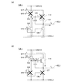
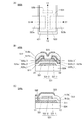
図1(A)は、FPC145(Flexible printed circuit)が接続された表示装置100の正面図である。図1(B)は、表示装置100の構成を説明するブロック図である。図2および図3は、ともに、図1(A)にA1−A2の一点鎖線で示す部位に相当する断面概略図である。図2および図3は、駆動回路部104aの一部と、表示部102の一部を示している。また、図2は表示素子として液晶素子を用いる液晶表示装置の一例を示している。図2に示す表示装置100は、FFS(Fringe Field Switching)モードで動作する液晶素子を例示している。また、図3は表示素子として発光素子を用いる発光表示装置の一例を示している。
<Display device configuration example>
FIG. 1A is a front view of a
表示装置100は、表示部102、駆動回路部104a、駆動回路部104b、および駆動回路部103を有する。駆動回路部104aおよび駆動回路部104bは、例えば走査線駆動回路として機能できる。また、駆動回路部103は、例えば信号線駆動回路として機能できる。なお、駆動回路部104a、および駆動回路部104bは、どちらか一方のみを設けて、他方を設けなくてもよい。また、表示部102を挟んで駆動回路部103と向き合う位置に、何らかの回路を設けてもよい。
The
なお、駆動回路部104a、駆動回路部104b、および駆動回路部103の総称として、「駆動回路」、「周辺回路」または「周辺駆動回路」という場合がある。
The
また、表示装置100は、各々が略平行に配設され、且つ、駆動回路部104a、および/または駆動回路部104bによって電位が制御されるn本(nは2以上の整数)の配線162と、各々が略平行に配設され、且つ、駆動回路部103によって電位が制御されるm本(mは2以上の整数)の配線163と、を有する。さらに、表示部102はn行m列のマトリクス状に配設された複数の画素110を有する。画素110は、画素回路および表示素子を有する。
Further, the
i行目(iは1以上n以下の整数)に配置された複数の画素110は、i本目の配線162と電気的に接続される。j列目(jは1以上m以下の整数)に配置された複数の画素110は、j本目の配線163と電気的に接続される。なお、本明細書等では、i本目の配線162を配線162_iと記す。また、本明細書等では、j本目の配線163を配線163_jと記す。
The plurality of
表示部102、駆動回路部104a、駆動回路部104b、および駆動回路部103は、第1の基板101上に設けられている。また、表示部102、駆動回路部104a、および駆動回路部104bを囲むようにして、シール材4005が設けられている。また、表示部102、駆動回路部104a、および駆動回路部104bの上に第2の基板106が設けられている。よって表示部102、駆動回路部104a、および駆動回路部104bは、第1の基板101とシール材105と第2の基板106とによって、表示素子と共に封止されている。
The
また、駆動回路部103は、別途用意された基板上に単結晶半導体または多結晶半導体で形成されている。駆動回路部103は、第1の基板101上のシール材105によって囲まれている領域とは異なる領域に実装されている。表示部102、駆動回路部104a、駆動回路部104b、および駆動回路部103に与えられる各種信号および電位は、FPC145から供給されている。
Further, the
なお、駆動回路部103の接続方法は、特に限定されるものではなく、ワイヤボンディング、COG(Chip On Glass)法、TCP(Tape Carrier Package)法、COF(Chip On Film)法などを用いることができる。図1(A)は、COG法により駆動回路部103を実装する例である。
The connection method of the
また、本明細書などにおいて、表示装置とは、表示素子が封止された状態にあるパネルと、該パネルにコントローラを含むIC等を実装した状態にあるモジュールとを含む場合がある。 Further, in the present specification and the like, the display device may include a panel in which the display element is sealed and a module in which an IC or the like including a controller is mounted on the panel.
〔断面構成例〕
表示装置100は電極143を有しており、電極143はFPC145が有する端子と異方性導電層144を介して、電気的に接続されている(図2および図3参照。)。また、電極143は、電極142を介して配線141と電気的に接続されている。
[Cross-section configuration example]
The
電極143は、第1の電極層117を形成した導電層の他の一部で形成される。電極142は、トランジスタ112、トランジスタ172、トランジスタ114、およびトランジスタ136のソース電極およびドレイン電極を形成した導電層の他の一部で形成される。配線141は、トランジスタ112、トランジスタ114、およびトランジスタ136のゲート電極を形成した導電層の他の一部で形成される。
The
表示部102、駆動回路部104a、および駆動回路部104bは、それぞれが複数のトランジスタを有する。図2では、表示部102に含まれるトランジスタ112と、駆動回路部104aに含まれるトランジスタ114およびトランジスタ136と、を例示している。図3では、表示部102に含まれるトランジスタ172およびトランジスタ112と、駆動回路部104aに含まれるトランジスタ114およびトランジスタ136と、を例示している。なお、本実施の形態では、トランジスタ112、トランジスタ172、トランジスタ114、およびトランジスタ136としてトップゲート型のトランジスタを例示している。
The
また、図2では、トランジスタ112、トランジスタ114、およびトランジスタ136上に、絶縁層149、絶縁層115、および絶縁層116が設けられている。図3では、トランジスタ172、トランジスタ112、トランジスタ114、およびトランジスタ136上に、絶縁層149、絶縁層115、および絶縁層116が設けられ、絶縁層116の上に隔壁132が設けられている。
Further, in FIG. 2, an insulating
また、トランジスタ112、トランジスタ172、トランジスタ114、およびトランジスタ136は、絶縁層146上に設けられている。加えて、トランジスタ112、トランジスタ172、トランジスタ114、およびトランジスタ136は、絶縁層146上に形成された電極147を有し、電極147上に絶縁層111が形成されている。電極147はバックゲート電極として機能することができる。表示装置100に用いるトランジスタの構造は、トップゲート型に限らずボトムゲート型であってもよい。なお、本発明の一態様に用いることができるトランジスタの構造については、別途詳細に説明する。
Further, the
また、トランジスタ114と基板101の間に絶縁層161が形成されている。絶縁層161は蓄熱層として機能する。
Further, an insulating
また、図2および図3に示す表示装置は、容量素子113を有する。容量素子113は、トランジスタ112のゲート電極を形成した導電層と同じ導電層の他の一部で形成された電極と、電極148が、絶縁層111介して重なる領域を有する。電極148は、電極147を形成した導電層の他の一部で形成されている。
Further, the display device shown in FIGS. 2 and 3 has a
一般に、表示装置の画素部に設けられる容量素子の容量は、画素部に配置されるトランジスタのリーク電流等を考慮して、所定の期間の間電荷を保持できるように設定される。容量素子の容量は、トランジスタのオフ電流等を考慮して設定すればよい。 Generally, the capacitance of the capacitance element provided in the pixel portion of the display device is set so as to hold the electric charge for a predetermined period in consideration of the leakage current of the transistor arranged in the pixel portion. The capacitance of the capacitive element may be set in consideration of the off-current of the transistor and the like.
例えば、金属酸化物の一種である酸化物半導体のバンドギャップは2eV以上あるため、チャネルが形成される半導体層に酸化物半導体を用いたトランジスタ(「OSトランジスタ」ともいう。)は、オフ電流を極めて小さくすることができる。具体的には、ソースとドレイン間の電圧が3.5V、室温(25℃)下において、チャネル幅1μm当たりのオフ電流を1×10⁻²⁰A未満、1×10⁻²²A未満、あるいは1×10⁻²⁴A未満とすることができる。すなわち、オンオフ比を20桁以上150桁以下とすることができる。 For example, since the bandgap of an oxide semiconductor, which is a type of metal oxide, is 2 eV or more, a transistor using an oxide semiconductor in the semiconductor layer on which a channel is formed (also referred to as an “OS transistor”) has an off-current. It can be extremely small. Specifically, voltage is 3.5V between the source and the drain, at at room temperature (25 ° C.), 1 × less than 10 -20 A state current per channel width 1 [mu] m, 1 × 10 below -22 A, or 1 It can be less than × 10-24A. That is, the on / off ratio can be 20 digits or more and 150 digits or less.
例えば、液晶表示装置の画素部にOSトランジスタを用いることにより、容量素子113の容量を、液晶容量に対して1/3以下、さらには1/5以下とすることができる。また、OSトランジスタを用いることにより、容量素子113の形成を省略することもできる。
For example, by using an OS transistor in the pixel portion of the liquid crystal display device, the capacity of the
図2において、表示部102に設けられたトランジスタ112は表示素子と電気的に接続する。また、図3において、表示部102に設けられたトランジスタ172は表示素子と電気的に接続する。
In FIG. 2, the
〔液晶表示装置の断面構成例〕
前述した通り、図2は表示素子として液晶素子121を用いた液晶表示装置の一例を示している。図2において、液晶素子121は、第1の電極層117、第2の電極層118、および液晶層124を含む。なお、液晶層124を挟持するように、絶縁層122および絶縁層123が設けられている。絶縁層122および絶縁層123は、配向膜として機能する。第2の電極層118は絶縁層116の上に設けられている。第2の電極層118は、絶縁層119を介して第1の電極層117と互いに重なる領域を有する。
[Example of cross-sectional configuration of liquid crystal display device]
As described above, FIG. 2 shows an example of a liquid crystal display device using the
またスペーサ125は絶縁層を選択的にエッチングすることで得られる柱状のスペーサであり、絶縁層122と絶縁層123との間隔(セルギャップ)を制御するために設けられている。なお、スペーサ125として、球状のスペーサを用いても良い。
The
また、必要に応じて、ブラックマトリクス(遮光層)、着色層(カラーフィルタ)、偏光部材、位相差部材、反射防止部材などの光学部材(光学基板)などを適宜設けてもよい。例えば、偏光基板および位相差基板による円偏光を用いてもよい。また、光源としてバックライト、サイドライトなどを用いてもよい。また、上記バックライト、およびサイドライトとして、マイクロLEDなどを用いても良い。 Further, if necessary, an optical member (optical substrate) such as a black matrix (light-shielding layer), a colored layer (color filter), a polarizing member, a retardation member, and an antireflection member may be appropriately provided. For example, circularly polarized light using a polarizing substrate and a retardation substrate may be used. Further, a backlight, a side light or the like may be used as the light source. Further, as the backlight and the side light, a micro LED or the like may be used.
図2に示す表示装置100では、第2の基板106と第2の絶縁層123の間に、遮光層151、着色層152、および絶縁層153が設けられている。
In the
遮光層として用いることのできる材料としては、カーボンブラック、チタンブラック、金属、金属酸化物、複数の金属酸化物の固溶体を含む複合酸化物等が挙げられる。遮光層は、樹脂材料を含む膜であってもよいし、金属などの無機材料の薄膜であってもよい。また、遮光層に、着色層の材料を含む膜の積層膜を用いることもできる。例えば、ある色の光を透過する着色層に用いる材料を含む膜と、他の色の光を透過する着色層に用いる材料を含む膜との積層構造を用いることができる。着色層と遮光層の材料を共通化することで、装置を共通化できるほか工程を簡略化できるため好ましい。 Examples of the material that can be used as the light-shielding layer include carbon black, titanium black, metal, metal oxide, and composite oxide containing a solid solution of a plurality of metal oxides. The light-shielding layer may be a film containing a resin material or a thin film of an inorganic material such as metal. Further, as the light-shielding layer, a laminated film of a film containing a material of a colored layer can also be used. For example, a laminated structure of a film containing a material used for a colored layer that transmits light of a certain color and a film containing a material used for a colored layer that transmits light of another color can be used. By using the same material for the colored layer and the light-shielding layer, it is preferable because the device can be shared and the process can be simplified.
着色層に用いることのできる材料としては、金属材料、樹脂材料、顔料または染料が含まれた樹脂材料などが挙げられる。遮光層および着色層の形成方法は、前述した各層の形成方法と同様に行なえばよい。例えば、インクジェット法などで行なってもよい。 Examples of the material that can be used for the colored layer include a metal material, a resin material, a resin material containing a pigment or a dye, and the like. The method for forming the light-shielding layer and the colored layer may be the same as the method for forming each layer described above. For example, it may be performed by an inkjet method or the like.
〔発光表示装置の断面構成例〕
また、前述した通り、図3は表示素子としてエレクトロルミネッセンスを利用する発光素子(「EL素子」ともいう。)を用いた発光表示装置の一例を示している。EL素子は、一対の電極の間に発光性の化合物を含む層(「EL層」ともいう。)を有する。一対の電極間に、EL素子の閾値電圧よりも大きい電位差を生じさせると、EL層に陽極側から正孔が注入され、陰極側から電子が注入される。注入された電子と正孔はEL層において再結合し、EL層に含まれる発光物質が発光する。
[Cross-sectional configuration example of light emitting display device]
Further, as described above, FIG. 3 shows an example of a light emitting display device using a light emitting element (also referred to as an “EL element”) that utilizes electroluminescence as a display element. The EL element has a layer (also referred to as an "EL layer") containing a luminescent compound between a pair of electrodes. When a potential difference larger than the threshold voltage of the EL element is generated between the pair of electrodes, holes are injected into the EL layer from the anode side and electrons are injected from the cathode side. The injected electrons and holes recombine in the EL layer, and the luminescent substance contained in the EL layer emits light.
また、EL素子は、発光材料が有機化合物であるか、無機化合物であるかによって区別され、一般的に、前者は有機EL素子、後者は無機EL素子と呼ばれている。 Further, the EL element is distinguished by whether the light emitting material is an organic compound or an inorganic compound, and the former is generally called an organic EL element and the latter is called an inorganic EL element.
有機EL素子は、電圧を印加することにより、一方の電極から電子、他方の電極から正孔がそれぞれEL層に注入される。そして、それらキャリア(電子および正孔)が再結合することにより、発光性の有機化合物が励起状態を形成し、その励起状態が基底状態に戻る際に発光する。このようなメカニズムから、このような発光素子は、電流励起型の発光素子と呼ばれる。 By applying a voltage to the organic EL element, electrons are injected into the EL layer from one electrode and holes are injected into the EL layer from the other electrode. Then, when those carriers (electrons and holes) are recombined, the luminescent organic compound forms an excited state, and when the excited state returns to the ground state, it emits light. From such a mechanism, such a light emitting element is called a current excitation type light emitting element.
なお、EL層は、発光性の化合物以外に、正孔注入性の高い物質、正孔輸送性の高い物質、正孔ブロック材料、電子輸送性の高い物質、電子注入性の高い物質、またはバイポーラ性の物質(電子輸送性および正孔輸送性が高い物質)などを有していてもよい。 In addition to the luminescent compound, the EL layer is a substance having a high hole injecting property, a substance having a high hole transporting property, a hole blocking material, a substance having a high electron transporting property, a substance having a high electron injecting property, or a bipolar. It may have a sex substance (a substance having high electron transport property and hole transport property) and the like.
EL層は、蒸着法(真空蒸着法を含む)、転写法、印刷法、インクジェット法、塗布法などの方法で形成することができる。 The EL layer can be formed by a method such as a thin-film deposition method (including a vacuum vapor deposition method), a transfer method, a printing method, an inkjet method, or a coating method.
無機EL素子は、その素子構成により、分散型無機EL素子と薄膜型無機EL素子とに分類される。分散型無機EL素子は、発光材料の粒子をバインダ中に分散させた発光層を有するものであり、発光メカニズムはドナー準位とアクセプター準位を利用するドナー−アクセプター再結合型発光である。薄膜型無機EL素子は、発光層を誘電体層で挟み込み、さらにそれを電極で挟んだ構造であり、発光メカニズムは金属イオンの内殻電子遷移を利用する局在型発光である。なお、ここでは、発光素子として有機EL素子を用いて説明する。 The inorganic EL element is classified into a dispersed inorganic EL element and a thin film type inorganic EL element according to the element configuration. The dispersed inorganic EL element has a light emitting layer in which particles of a light emitting material are dispersed in a binder, and the light emitting mechanism is donor-acceptor recombination type light emission utilizing a donor level and an acceptor level. The thin-film inorganic EL element has a structure in which a light emitting layer is sandwiched between dielectric layers and further sandwiched between electrodes, and the light emitting mechanism is localized light emission utilizing the inner-shell electron transition of metal ions. Here, an organic EL element will be used as the light emitting element.
発光素子は発光を取り出すために少なくとも一対の電極の一方が透明であればよい。そして、基板上にトランジスタおよび発光素子を形成し、当該基板とは逆側の面から発光を取り出す上面射出(トップエミッション)構造や、基板側の面から発光を取り出す下面射出(ボトムエミッション)構造や、両面から発光を取り出す両面射出(デュアルエミッション)構造の発光素子があり、どの射出構造の発光素子も適用することができる。 The light emitting element may have at least one of a pair of electrodes transparent in order to extract light. Then, a top emission (top emission) structure in which a transistor and a light emitting element are formed on the substrate and light emission is taken out from the surface opposite to the substrate, or a bottom injection (bottom emission) structure in which light emission is taken out from the surface on the substrate side. , There is a light emitting element having a double-sided emission (dual emission) structure that extracts light emission from both sides, and any light emitting element having an injection structure can be applied.
表示素子である発光素子131は、表示部102に設けられたトランジスタ172と電気的に接続している。なお発光素子131の構成は、第1の電極層117、発光層133、第2の電極層118の積層構造であるが、この構成に限定されない。発光素子131から取り出す光の方向などに合わせて、発光素子131の構成は適宜変えることができる。
The
隔壁132は、有機絶縁材料、または無機絶縁材料を用いて形成する。特に感光性の樹脂材料を用い、第1の電極層117上に開口部を形成し、その開口部の側面が連続した曲率を持って形成される傾斜面となるように形成することが好ましい。
The
発光層133は、単数の層で構成されていても、複数の層が積層されるように構成されていてもどちらでも良い。
The
発光素子131の発光色は、発光層133を構成する材料によって、白、赤、緑、青、シアン、マゼンタ、または黄などに変化させることができる。
The emission color of the
カラー表示を実現する方法としては、発光色が白色の発光素子131と着色層を組み合わせて行う方法と、画素毎に発光色の異なる発光素子131を設ける方法がある。前者の方法は後者の方法よりも生産性が高い。一方、後者の方法では画素毎に発光層133を作り分ける必要があるため、前者の方法よりも生産性が劣る。ただし、後者の方法では、前者の方法よりも色純度の高い発光色を得ることができる。後者の方法に加えて、発光素子131にマイクロキャビティ構造を付与することにより色純度をさらに高めることができる。
As a method of realizing color display, there are a method of combining a
なお、発光層133は、量子ドットなどの無機化合物を有していてもよい。例えば、量子ドットを発光層に用いることで、発光材料として機能させることもできる。
The
発光素子131に酸素、水素、水分、二酸化炭素等が侵入しないように、第2の電極層118および隔壁132上に保護層を形成してもよい。保護層としては、窒化シリコン、窒化酸化シリコン、酸化アルミニウム、窒化アルミニウム、酸化窒化アルミニウム、窒化酸化アルミニウム、DLC(Diamond Like Carbon)などを形成することができる。また、第1の基板101、第2の基板106、およびシール材105によって封止された空間には充填材135が設けられ密封されている。このように、外気に曝されないように気密性が高く、脱ガスの少ない保護フィルム(貼り合わせフィルム、紫外線硬化樹脂フィルム等)やカバー材でパッケージング(封入)することが好ましい。
A protective layer may be formed on the
充填材135としては窒素やアルゴンなどの不活性な気体の他に、紫外線硬化樹脂または熱硬化樹脂を用いることができ、PVC(ポリビニルクロライド)、アクリル樹脂、ポリイミド、エポキシ樹脂、シリコーン樹脂、PVB(ポリビニルブチラル)またはEVA(エチレンビニルアセテート)などを用いることができる。また、充填材135に乾燥剤が含まれていてもよい。
As the
シール材105には、ガラスフリットなどのガラス材料や、二液混合型の樹脂などの常温で硬化する硬化樹脂、光硬化性の樹脂、熱硬化性の樹脂などの樹脂材料を用いることができる。また、シール材105に乾燥剤が含まれていてもよい。
As the sealing
また、必要であれば、発光素子の射出面に偏光板、または円偏光板(楕円偏光板を含む)、位相差板(λ/4板、λ/2板)、カラーフィルタなどの光学フィルムを適宜設けてもよい。また、偏光板または円偏光板に反射防止膜を設けてもよい。例えば、表面の凹凸により反射光を拡散し、映り込みを低減できるアンチグレア処理を施すことができる。 If necessary, an optical film such as a polarizing plate or a circular polarizing plate (including an elliptical polarizing plate), a retardation plate (λ / 4 plate, λ / 2 plate), and a color filter is attached to the ejection surface of the light emitting element. It may be provided as appropriate. Further, an antireflection film may be provided on the polarizing plate or the circular polarizing plate. For example, it is possible to apply an anti-glare treatment that can diffuse the reflected light due to the unevenness of the surface and reduce the reflection.
また、発光素子をマイクロキャビティ構造とすることで、色純度の高い光を取り出すことができる。また、マイクロキャビティ構造とカラーフィルタを組み合わせることで、映り込みが低減し、表示画像の視認性を高めることができる。 Further, by forming the light emitting element with a microcavity structure, it is possible to extract light having high color purity. Further, by combining the microcavity structure and the color filter, reflection can be reduced and the visibility of the displayed image can be improved.
表示素子に電圧を印加する第1の電極層および第2の電極層(画素電極層、共通電極層、対向電極層などともいう)においては、取り出す光の方向、電極層が設けられる場所、および電極層のパターン構造によって透光性、反射性を選択すればよい。 In the first electrode layer and the second electrode layer (also referred to as a pixel electrode layer, a common electrode layer, a counter electrode layer, etc.) for applying a voltage to the display element, the direction of the light to be taken out, the place where the electrode layer is provided, and the place where the electrode layer is provided. Translucency and reflectivity may be selected according to the pattern structure of the electrode layer.
第1の電極層117、第2の電極層118は、酸化タングステンを含むインジウム酸化物、酸化タングステンを含むインジウム亜鉛酸化物、酸化チタンを含むインジウム酸化物、インジウム錫酸化物、酸化チタンを含むインジウム錫酸化物、インジウム亜鉛酸化物、酸化ケイ素を添加したインジウム錫酸化物などの透光性を有する導電性材料を用いることができる。
The
また、第1の電極層117および第2の電極層118は、タングステン(W)、モリブデン(Mo)、ジルコニウム(Zr)、ハフニウム(Hf)、バナジウム(V)、ニオブ(Nb)、タンタル(Ta)、クロム(Cr)、コバルト(Co)、ニッケル(Ni)、チタン(Ti)、白金(Pt)、アルミニウム(Al)、銅(Cu)、銀(Ag)などの金属、またはその合金、もしくはその金属窒化物から一種以上を用いて形成することができる。
Further, the
また、第1の電極層117および第2の電極層118として、導電性高分子(導電性ポリマーともいう)を含む導電性組成物を用いて形成することができる。導電性高分子としては、いわゆるπ電子共役系導電性高分子を用いることができる。例えば、ポリアニリン若しくはその誘導体、ポリピロール若しくはその誘導体、ポリチオフェン若しくはその誘導体、または、アニリン、ピロールおよびチオフェンの2種以上からなる共重合体若しくはその誘導体などがあげられる。
Further, the
〔構成材料について〕
本発明の一態様の表示装置または半導体装置に用いることができる材料などについて説明しておく。
[Constituent materials]
A material and the like that can be used for the display device or the semiconductor device of one aspect of the present invention will be described.
[基板]
基板に用いる材料に大きな制限はない。目的に応じて、透光性の有無や加熱処理に耐えうる程度の耐熱性などを勘案して決定すればよい。例えばバリウムホウケイ酸ガラスやアルミノホウケイ酸ガラスなどのガラス基板、セラミック基板、石英基板、サファイア基板などを用いることができる。また、半導体基板、可撓性基板(フレキシブル基板)、貼り合わせフィルム、基材フィルムなどを用いてもよい。
[substrate]
There are no major restrictions on the materials used for the substrate. Depending on the purpose, it may be determined in consideration of the presence or absence of translucency and the heat resistance to the extent that it can withstand heat treatment. For example, a glass substrate such as barium borosilicate glass or aluminoborosilicate glass, a ceramic substrate, a quartz substrate, a sapphire substrate, or the like can be used. Further, a semiconductor substrate, a flexible substrate (flexible substrate), a bonding film, a base film, or the like may be used.
半導体基板としては、例えば、シリコン、もしくはゲルマニウムなどを材料とした単体半導体基板、または炭化シリコン、シリコンゲルマニウム、ヒ化ガリウム、リン化インジウム、酸化亜鉛、もしくは酸化ガリウムを材料とした化合物半導体基板などがある。また、半導体基板は、単結晶半導体であってもよいし、多結晶半導体であってもよい。 Examples of the semiconductor substrate include a single semiconductor substrate made of silicon or germanium, or a compound semiconductor substrate made of silicon carbide, silicon germanium, gallium arsenide, indium phosphide, zinc oxide, or gallium oxide. be. Further, the semiconductor substrate may be a single crystal semiconductor or a polycrystalline semiconductor.
また、基板として、例えば、第6世代(1500mm×1850mm)、第7世代(1870mm×2200mm)、第8世代(2200mm×2400mm)、第9世代(2400mm×2800mm)、第10世代(2950mm×3400mm)等の面積が大きなガラス基板を用いることができる。これにより、大型の表示装置を作製することができる。また、基板が大型化されることで、1枚の基板からより多くの表示装置を生産でき、生産コストを削減することができる。 Further, as the substrate, for example, the 6th generation (1500 mm × 1850 mm), the 7th generation (1870 mm × 2200 mm), the 8th generation (2200 mm × 2400 mm), the 9th generation (2400 mm × 2800 mm), and the 10th generation (2950 mm × 3400 mm). ) Etc., a glass substrate having a large area can be used. As a result, a large display device can be manufactured. Further, by increasing the size of the substrate, more display devices can be produced from one substrate, and the production cost can be reduced.
なお、表示装置100の可撓性を高めるため、基板として可撓性基板(フレキシブル基板)、貼り合わせフィルム、基材フィルムなどを用いてもよい。
In addition, in order to increase the flexibility of the
可撓性基板、貼り合わせフィルム、基材フィルムなどの材料としては、例えば、ポリエチレンテレフタレート(PET)、ポリエチレンナフタレート(PEN)等のポリエステル樹脂、ポリアクリロニトリル樹脂、アクリル樹脂、ポリイミド樹脂、ポリメチルメタクリレート樹脂、ポリカーボネイト(PC)樹脂、ポリエーテルスルホン(PES)樹脂、ポリアミド樹脂(ナイロン、アラミド等)、ポリシロキサン樹脂、シクロオレフィン樹脂、ポリスチレン樹脂、ポリアミドイミド樹脂、ポリウレタン樹脂、ポリ塩化ビニル樹脂、ポリ塩化ビニリデン樹脂、ポリプロピレン樹脂、ポリテトラフルオロエチレン(PTFE)樹脂、ABS樹脂、セルロースナノファイバーなどを用いることができる。 Examples of materials such as flexible substrates, laminated films, and base film include polyester resins such as polyethylene terephthalate (PET) and polyethylene naphthalate (PEN), polyacrylonitrile resins, acrylic resins, polyimide resins, and polymethyl methacrylates. Resin, Polycarbonate (PC) resin, polyether sulfone (PES) resin, polyamide resin (nylon, aramid, etc.), polysiloxane resin, cycloolefin resin, polystyrene resin, polyamideimide resin, polyurethane resin, polyvinyl chloride resin, polychloride Vinylidene resin, polypropylene resin, polytetrafluoroethylene (PTFE) resin, ABS resin, cellulose nanofibers and the like can be used.
基板として上記材料を用いることにより、軽量な表示装置を提供することができる。また、基板として上記材料を用いることにより、衝撃に強い表示装置を提供することができる。また、基板として上記材料を用いることにより、破損しにくい表示装置を提供することができる。 By using the above material as the substrate, a lightweight display device can be provided. Further, by using the above material as the substrate, it is possible to provide a display device that is strong against impact. Further, by using the above material as the substrate, it is possible to provide a display device that is not easily damaged.
基板に用いる可撓性基板は、線膨張率が低いほど環境による変形が抑制されて好ましい。基板に用いる可撓性基板は、例えば、線膨張率が1×10⁻³/K以下、5×10−5/K以下、または1×10−5/K以下である材質を用いればよい。特に、アラミドは、線膨張率が低いため、可撓性基板として好適である。 As for the flexible substrate used for the substrate, the lower the coefficient of linear expansion, the more the deformation due to the environment is suppressed, which is preferable. As the flexible substrate used for the substrate, for example, a material having a linear expansion coefficient of 1 × 10 -3 / K or less, 5 × 10 -5 / K or less, or 1 × 10 -5 / K or less may be used. In particular, aramid is suitable as a flexible substrate because of its low coefficient of linear expansion.
[導電層]
トランジスタのゲート、ソースおよびドレインのほか、表示装置を構成する各種配線および電極などの導電層に用いることのできる導電性材料としては、アルミニウム(Al)、クロム(Cr)、銅(Cu)、銀(Ag)、金(Au)、白金(Pt)、タンタル(Ta)、ニッケル(Ni)、チタン(Ti)、モリブデン(Mo)、タングステン(W)、ハフニウム(Hf)、バナジウム(V)、ニオブ(Nb)、マンガン(Mn)、マグネシウム(Mg)、ジルコニウム(Zr)、ベリリウム(Be)等から選ばれた金属元素、上述した金属元素を成分とする合金、または上述した金属元素を組み合わせた合金などを用いることができる。また、リン等の不純物元素を含有させた多結晶シリコンに代表される半導体、ニッケルシリサイドなどのシリサイドを用いてもよい。導電性材料の形成方法は特に限定されず、蒸着法、CVD法、スパッタリング法、スピンコート法などの各種形成方法を用いることができる。
[Conductive layer]
In addition to the gate, source and drain of the transistor, the conductive materials that can be used for the conductive layers such as various wirings and electrodes that make up the display device include aluminum (Al), chromium (Cr), copper (Cu), and silver. (Ag), gold (Au), platinum (Pt), tantalum (Ta), nickel (Ni), titanium (Ti), molybdenum (Mo), tungsten (W), hafnium (Hf), vanadium (V), niobium A metal element selected from (Nb), manganese (Mn), magnesium (Mg), zirconium (Zr), beryllium (Be), etc., an alloy containing the above-mentioned metal element as a component, or an alloy obtained by combining the above-mentioned metal element. Etc. can be used. Further, a semiconductor typified by polycrystalline silicon containing an impurity element such as phosphorus, and a silicide such as nickel silicide may be used. The method for forming the conductive material is not particularly limited, and various forming methods such as a vapor deposition method, a CVD method, a sputtering method, and a spin coating method can be used.
また、導電性材料として、Cu−X合金(Xは、Mn、Ni、Cr、Fe、Co、Mo、Ta、またはTi)を適用してもよい。Cu−X合金で形成した層は、ウエットエッチングプロセスで加工できるため、製造コストを抑制することが可能となる。また、導電性材料として、チタン、タンタル、タングステン、モリブデン、クロム、ネオジム、スカンジウムから選ばれた一または複数の元素を含むアルミニウム合金を用いてもよい。 Further, as the conductive material, a Cu—X alloy (X is Mn, Ni, Cr, Fe, Co, Mo, Ta, or Ti) may be applied. Since the layer formed of the Cu—X alloy can be processed by a wet etching process, the manufacturing cost can be suppressed. Further, as the conductive material, an aluminum alloy containing one or more elements selected from titanium, tantalum, tungsten, molybdenum, chromium, neodymium, and scandium may be used.
また、導電層に用いることのできる導電性材料として、インジウム錫酸化物、酸化タングステンを含むインジウム酸化物、酸化タングステンを含むインジウム亜鉛酸化物、酸化チタンを含むインジウム酸化物、酸化チタンを含むインジウム錫酸化物、インジウム亜鉛酸化物、酸化ケイ素を添加したインジウム錫酸化物などの、酸素を有する導電性材料を用いることもできる。また、窒化チタン、窒化タンタル、窒化タングステンなどの、窒素を含む導電性材料を用いることもできる。また、導電層を、酸素を有する導電性材料、窒素を含む導電性材料、前述した金属元素を含む材料を適宜組み合わせた積層構造とすることもできる。 Further, as a conductive material that can be used for the conductive layer, indium tin oxide, indium oxide containing tungsten oxide, indium zinc oxide containing tungsten oxide, indium oxide containing titanium oxide, and indium tin containing titanium oxide. Conductive materials having oxygen, such as oxides, indium zinc oxides, and indium tin oxides to which silicon oxide has been added, can also be used. Further, a conductive material containing nitrogen such as titanium nitride, tantalum nitride, and tungsten nitride can also be used. Further, the conductive layer may have a laminated structure in which a conductive material having oxygen, a conductive material containing nitrogen, and a material containing the above-mentioned metal element are appropriately combined.
例えば、導電層を、シリコンを含むアルミニウム層の単層構造、アルミニウム層上にチタン層を積層する二層構造、窒化チタン層上にチタン層を積層する二層構造、窒化チタン層上にタングステン層を積層する二層構造、窒化タンタル層上にタングステン層を積層する二層構造、チタン層と、そのチタン層上にアルミニウム層を積層し、さらにその上にチタン層を積層する三層構造としてもよい。 For example, the conductive layer has a single-layer structure of an aluminum layer containing silicon, a two-layer structure in which a titanium layer is laminated on an aluminum layer, a two-layer structure in which a titanium layer is laminated on a titanium nitride layer, and a tungsten layer on a titanium nitride layer. As a two-layer structure in which the titanium layer is laminated, a two-layer structure in which the tungsten layer is laminated on the titanium nitride layer, a titanium layer, an aluminum layer on the titanium layer, and a titanium layer on the titanium layer. good.
また、上記の導電性材料で形成される導電層を複数積層して用いてもよい。例えば、導電層を前述した金属元素を含む材料と酸素を含む導電性材料を組み合わせた積層構造としてもよい。また、前述した金属元素を含む材料と、窒素を含む導電性材料を組み合わせた積層構造としてもよい。また、前述した金属元素を含む材料、酸素を含む導電性材料、および窒素を含む導電性材料を組み合わせた積層構造としてもよい。 Further, a plurality of conductive layers formed of the above conductive materials may be laminated and used. For example, the conductive layer may have a laminated structure in which the above-mentioned material containing a metal element and a conductive material containing oxygen are combined. Further, a laminated structure may be formed in which the above-mentioned material containing a metal element and a conductive material containing nitrogen are combined. Further, a laminated structure may be formed in which the above-mentioned material containing a metal element, a conductive material containing oxygen, and a conductive material containing nitrogen are combined.
例えば、導電層を、インジウムまたは亜鉛の少なくとも一方と酸素とを含む導電層上に、銅を含む導電層を積層し、さらにその上にインジウムまたは亜鉛の少なくとも一方と酸素とを含む導電層を積層する三層構造としてもよい。この場合、銅を含む導電層の側面もインジウムまたは亜鉛の少なくとも一方と酸素とを含む導電層で覆うことが好ましい。また、例えば、導電層としてインジウムまたは亜鉛の少なくとも一方と酸素とを含む導電層を複数積層して用いてもよい。 For example, the conductive layer is formed by laminating a conductive layer containing copper on a conductive layer containing at least one of indium or zinc and oxygen, and further laminating a conductive layer containing at least one of indium or zinc and oxygen on the conductive layer. It may have a three-layer structure. In this case, it is preferable that the side surface of the conductive layer containing copper is also covered with the conductive layer containing at least one of indium or zinc and oxygen. Further, for example, a plurality of conductive layers containing at least one of indium or zinc and oxygen may be laminated and used as the conductive layer.
[絶縁層]
各絶縁層は、窒化アルミニウム、酸化アルミニウム、窒化酸化アルミニウム、酸化窒化アルミニウム、酸化マグネシウム、窒化シリコン、酸化シリコン、窒化酸化シリコン、酸化窒化シリコン、酸化ガリウム、酸化ゲルマニウム、酸化イットリウム、酸化ジルコニウム、酸化ランタン、酸化ネオジム、酸化ハフニウム、酸化タンタル、アルミニウムシリケートなどから選ばれた材料を、単層でまたは積層して用いる。また、酸化物材料、窒化物材料、酸化窒化物材料、窒化酸化物材料のうち、複数の材料を混合した材料を用いてもよい。
[Insulation layer]
Each insulating layer is made of aluminum nitride, aluminum oxide, aluminum nitride, aluminum oxide, magnesium oxide, silicon nitride, silicon oxide, silicon nitride, silicon nitride, gallium oxide, germanium oxide, yttrium oxide, zirconium oxide, and lanthanum oxide. , Neodim oxide, Hafnium oxide, Tantal oxide, Aluminum silicate, etc. are used in a single layer or in a laminated manner. Further, among the oxide material, the nitride material, the oxide nitride material, and the nitride oxide material, a material obtained by mixing a plurality of materials may be used.
なお、本明細書などにおいて、窒化酸化物とは、酸素よりも窒素の含有量が多い化合物をいう。また、酸化窒化物とは、窒素よりも酸素の含有量が多い化合物をいう。なお、各元素の含有量は、例えば、ラザフォード後方散乱法(RBS:Rutherford Backscattering Spectrometry)等を用いて測定することができる。 In the present specification and the like, the nitride oxide refers to a compound having a higher nitrogen content than oxygen. The oxidative nitride refers to a compound having a higher oxygen content than nitrogen. The content of each element can be measured by using, for example, Rutherford Backscattering Spectrometry (RBS) or the like.
特に絶縁層146および絶縁層149は、不純物が透過しにくい絶縁性材料を用いて形成することが好ましい。例えば、ホウ素、炭素、窒素、酸素、フッ素、マグネシウム、アルミニウム、シリコン、リン、塩素、アルゴン、ガリウム、ゲルマニウム、イットリウム、ジルコニウム、ランタン、ネオジム、ハフニウムまたはタンタルを含む絶縁材料を、単層で、または積層で用いればよい。不純物が透過しにくい絶縁性材料の一例として、酸化アルミニウム、窒化アルミニウム、酸化窒化アルミニウム、窒化酸化アルミニウム、酸化ガリウム、酸化ゲルマニウム、酸化イットリウム、酸化ジルコニウム、酸化ランタン、酸化ネオジム、酸化ハフニウム、酸化タンタル、窒化シリコンなどを挙げることができる。
In particular, the insulating
絶縁層146に不純物が透過しにくい絶縁性材料を用いることで、基板101側からの不純物の拡散を抑制し、トランジスタの信頼性を高めることができる。絶縁層149に不純物が透過しにくい絶縁性材料を用いることで、絶縁層149よりも上側からの不純物の拡散を抑制し、トランジスタの信頼性を高めることができる。
By using an insulating material in which impurities do not easily permeate into the insulating
また、絶縁層として平坦化層として機能できる絶縁層を用いてもよい。平坦化層として機能できる絶縁層としては、ポリイミド、アクリル樹脂、ベンゾシクロブテン樹脂、ポリアミド、エポキシ樹脂等の、耐熱性を有する有機材料を用いることができる。また上記有機材料の他に、低誘電率材料(low−k材料)、シロキサン樹脂、PSG(リンガラス)、BPSG(リンボロンガラス)等を用いることができる。なお、これらの材料で形成される絶縁層を複数積層してもよい。 Further, an insulating layer capable of functioning as a flattening layer may be used as the insulating layer. As the insulating layer that can function as the flattening layer, a heat-resistant organic material such as polyimide, acrylic resin, benzocyclobutene resin, polyamide, or epoxy resin can be used. In addition to the above organic materials, low dielectric constant materials (low-k materials), siloxane resins, PSG (phosphorus glass), BPSG (phosphorene glass) and the like can be used. A plurality of insulating layers formed of these materials may be laminated.
なお、シロキサン樹脂とは、シロキサン系材料を出発材料として形成されたSi−O−Si結合を含む樹脂に相当する。シロキサン樹脂は置換基としては有機基(例えばアルキル基やアリール基)やフルオロ基を用いても良い。また、有機基はフルオロ基を有していても良い。 The siloxane resin corresponds to a resin containing a Si—O—Si bond formed using a siloxane-based material as a starting material. As the substituent of the siloxane resin, an organic group (for example, an alkyl group or an aryl group) or a fluoro group may be used. Moreover, the organic group may have a fluoro group.
また、絶縁層などの表面にCMP処理を行なってもよい。CMP処理を行うことにより、試料表面の凹凸を低減し、この後形成される絶縁層や導電層の被覆性を高めることができる。 Further, the surface of the insulating layer or the like may be subjected to CMP treatment. By performing the CMP treatment, the unevenness of the sample surface can be reduced, and the covering property of the insulating layer and the conductive layer formed after that can be improved.
[半導体層]
トランジスタの半導体層に用いる半導体材料としては、非晶質半導体、結晶性を有する半導体(微結晶半導体、多結晶半導体、単結晶半導体、または一部に結晶領域を有する半導体)のいずれを用いてもよい。
[Semiconductor layer]
As the semiconductor material used for the semiconductor layer of the transistor, any of amorphous semiconductors and crystalline semiconductors (microcrystalline semiconductors, polycrystalline semiconductors, single crystal semiconductors, or semiconductors having a partially crystalline region) may be used. good.
また、例えば、トランジスタの半導体層に用いる半導体材料として、シリコンや、ゲルマニウム等を用いることができる。また、炭化シリコン、ガリウム砒素、金属酸化物、窒化物半導体などの化合物半導体や、有機半導体などを用いることができる。 Further, for example, silicon, germanium, or the like can be used as the semiconductor material used for the semiconductor layer of the transistor. Further, compound semiconductors such as silicon carbide, gallium arsenide, metal oxides and nitride semiconductors, organic semiconductors and the like can be used.
例えば、トランジスタに用いる半導体材料として、非晶質シリコン(アモルファスシリコン)を用いることができる。特に、非晶質シリコンは、量産性に優れ、大きな面積の基板に設けることも容易である。なお、一般に、トランジスタに用いる非晶質シリコンは水素を多く含む。このため、水素を多く含む非晶質シリコンを「水素化アモルファスシリコン」または「a−Si:H」と言う場合がある。また、アモルファスシリコンは、多結晶シリコンよりも低温で形成できるため、作製工程中の最高温度を下げることができる。よって、基板、導電層、および絶縁層などに、耐熱性の低い材料を用いることができる。 For example, amorphous silicon (amorphous silicon) can be used as the semiconductor material used for the transistor. In particular, amorphous silicon is excellent in mass productivity and can be easily provided on a substrate having a large area. In general, amorphous silicon used for transistors contains a large amount of hydrogen. Therefore, amorphous silicon containing a large amount of hydrogen may be referred to as "hydrogenated amorphous silicon" or "a-Si: H". Further, since amorphous silicon can be formed at a lower temperature than polycrystalline silicon, the maximum temperature during the manufacturing process can be lowered. Therefore, a material having low heat resistance can be used for the substrate, the conductive layer, the insulating layer, and the like.
また、トランジスタに用いる半導体材料として、微結晶シリコン、多結晶シリコン、単結晶シリコンなどの結晶性を有するシリコンを用いることもできる。特に、多結晶シリコンは、単結晶シリコンに比べて低温で形成でき、且つアモルファスシリコンに比べて高い電界効果移動度と高い信頼性を備える。 Further, as the semiconductor material used for the transistor, silicon having crystallinity such as microcrystalline silicon, polycrystalline silicon, and single crystal silicon can also be used. In particular, polycrystalline silicon can be formed at a lower temperature than single crystal silicon, and has higher field effect mobility and higher reliability than amorphous silicon.
また、トランジスタに用いる半導体材料として、金属酸化物の一種である酸化物半導体を用いることができる。代表的には、インジウムを含む酸化物半導体などを用いることができる。酸化物半導体は、アモルファスシリコンよりも高い電界効果移動度と高い信頼性が実現できる。また、酸化物半導体は量産性に優れ、大きな面積の基板に設けることも容易である。 Further, as the semiconductor material used for the transistor, an oxide semiconductor which is a kind of metal oxide can be used. Typically, an oxide semiconductor containing indium or the like can be used. Oxide semiconductors can achieve higher field-effect mobility and higher reliability than amorphous silicon. Further, the oxide semiconductor is excellent in mass productivity and can be easily provided on a substrate having a large area.
また、金属酸化物の一種である酸化物半導体はシリコンよりもバンドギャップが広く、キャリア密度が低いため、トランジスタの半導体層に用いることが好ましい。トランジスタの半導体層に酸化物半導体を用いると、トランジスタのオフ状態におけるソースとドレインの間に流れる電流を低減できるため好ましい。 Further, since an oxide semiconductor, which is a kind of metal oxide, has a wider bandgap and a lower carrier density than silicon, it is preferably used for the semiconductor layer of a transistor. It is preferable to use an oxide semiconductor for the semiconductor layer of the transistor because the current flowing between the source and the drain in the off state of the transistor can be reduced.
金属酸化物の一種である酸化物半導体は、エネルギーギャップが2eV以上であることが好ましく、2.5eV以上であることがより好ましく。3eV以上であることがさらに好ましい。このように、エネルギーギャップの広い酸化物半導体を用いることで、トランジスタのオフ電流を低減することができる。 The oxide semiconductor, which is a kind of metal oxide, preferably has an energy gap of 2 eV or more, and more preferably 2.5 eV or more. It is more preferably 3 eV or more. As described above, by using an oxide semiconductor having a wide energy gap, the off-current of the transistor can be reduced.
金属酸化物の一種である酸化物半導体は、例えば少なくともインジウム、亜鉛およびM(アルミニウム、チタン、ガリウム、ゲルマニウム、イットリウム、ジルコニウム、ランタン、セリウム、スズ、ネオジムまたはハフニウム等の金属)を含むIn−M−Zn系酸化物で表記される材料を含むことが好ましい。また、該酸化物半導体を用いたトランジスタの電気特性のばらつきを減らすため、それらと共に、スタビライザーを含むことが好ましい。 Oxide semiconductors, which are a type of metal oxide, include In-M containing at least indium, zinc and M (metals such as aluminum, titanium, gallium, germanium, yttrium, zirconium, lanthanum, cerium, tin, neodymium or hafnium). It is preferable to include a material represented by −Zn-based oxide. Further, in order to reduce variations in the electrical characteristics of the transistor using the oxide semiconductor, it is preferable to include a stabilizer together with them.
スタビライザーとしては、上記Mで記載の金属を含め、例えば、ガリウム、スズ、ハフニウム、アルミニウム、またはジルコニウム等がある。また、他のスタビライザーとしては、ランタノイドである、ランタン、セリウム、プラセオジム、ネオジム、サマリウム、ユウロピウム、ガドリニウム、テルビウム、ジスプロシウム、ホルミウム、エルビウム、ツリウム、イッテルビウム、ルテチウム等がある。 Examples of the stabilizer include gallium, tin, hafnium, aluminum, zirconium and the like, including the metal described in M above. Other stabilizers include lanthanoids such as lanthanide, cerium, praseodymium, neodymium, samarium, europium, gadolinium, terbium, dysprosium, holmium, erbium, thulium, ytterbium, and lutetium.
半導体層を構成する金属酸化物として、例えば、In−Ga−Zn系酸化物、In−Al−Zn系酸化物、In−Sn−Zn系酸化物、In−Hf−Zn系酸化物、In−La−Zn系酸化物、In−Ce−Zn系酸化物、In−Pr−Zn系酸化物、In−Nd−Zn系酸化物、In−Sm−Zn系酸化物、In−Eu−Zn系酸化物、In−Gd−Zn系酸化物、In−Tb−Zn系酸化物、In−Dy−Zn系酸化物、In−Ho−Zn系酸化物、In−Er−Zn系酸化物、In−Tm−Zn系酸化物、In−Yb−Zn系酸化物、In−Lu−Zn系酸化物、In−Sn−Ga−Zn系酸化物、In−Hf−Ga−Zn系酸化物、In−Al−Ga−Zn系酸化物、In−Sn−Al−Zn系酸化物、In−Sn−Hf−Zn系酸化物、In−Hf−Al−Zn系酸化物を用いることができる。 Examples of the metal oxide constituting the semiconductor layer include In-Ga-Zn-based oxide, In-Al-Zn-based oxide, In-Sn-Zn-based oxide, In-Hf-Zn-based oxide, and In-. La-Zn-based oxide, In-Ce-Zn-based oxide, In-Pr-Zn-based oxide, In-Nd-Zn-based oxide, In-Sm-Zn-based oxide, In-Eu-Zn-based oxide In-Gd-Zn-based oxide, In-Tb-Zn-based oxide, In-Dy-Zn-based oxide, In-Ho-Zn-based oxide, In-Er-Zn-based oxide, In-Tm -Zn-based oxide, In-Yb-Zn-based oxide, In-Lu-Zn-based oxide, In-Sn-Ga-Zn-based oxide, In-Hf-Ga-Zn-based oxide, In-Al- Ga-Zn-based oxides, In-Sn-Al-Zn-based oxides, In-Sn-Hf-Zn-based oxides, and In-Hf-Al-Zn-based oxides can be used.
なお、ここで、In−Ga−Zn系酸化物とは、InとGaとZnを主成分として有する酸化物という意味であり、InとGaとZnの比率は問わない。また、InとGaとZn以外の金属元素が入っていてもよい。 Here, the In-Ga-Zn-based oxide means an oxide containing In, Ga, and Zn as main components, and the ratio of In, Ga, and Zn does not matter. Further, a metal element other than In, Ga and Zn may be contained.
なお、トランジスタの半導体層に用いることができる金属酸化物については、他の実施の形態で詳細に説明する。 The metal oxide that can be used for the semiconductor layer of the transistor will be described in detail in another embodiment.
[各層の形成方法]
絶縁層、半導体層、電極や配線を形成するための導電層などは、スパッタリング法、化学気相堆積(CVD:Chemical Vapor Deposition)法、真空蒸着法、パルスレーザ堆積(PLD:Pulse Laser Deposition)法、原子層成膜(ALD:Atomic Layer Deposition)法などを用いて形成することができる。CVD法としては、プラズマ化学気相堆積(PECVD)法や、熱CVD法でもよい。熱CVD法の例として、有機金属化学気相堆積(MOCVD:Metal Organic CVD)法を用いてもよい。
[Formation method of each layer]
Insulating layers, semiconductor layers, conductive layers for forming electrodes and wiring are prepared by sputtering method, chemical vapor deposition (CVD) method, vacuum deposition method, pulse laser deposition (PLD) method. , Atomic layer deposition (ALD) method or the like can be used for formation. The CVD method may be a plasma chemical vapor deposition (PECVD) method or a thermal CVD method. As an example of the thermal CVD method, the metalorganic chemical vapor deposition (MOCVD) method may be used.
また、表示装置を構成する絶縁層、半導体層、電極や配線を形成するための導電層などは、スピンコート、ディップ、スプレー塗布、インクジェット、ディスペンス、スクリーン印刷、オフセット印刷、スリットコート、ロールコート、カーテンコート、ナイフコート等の方法により形成してもよい。 In addition, the insulating layer, semiconductor layer, conductive layer for forming electrodes and wiring, etc. that make up the display device include spin coating, dip, spray coating, inkjet, dispense, screen printing, offset printing, slit coating, roll coating, etc. It may be formed by a method such as a curtain coat or a knife coat.
PECVD法は、比較的低温で高品質の膜が得られる。MOCVD法、ALD法、または熱CVD法などの、成膜時にプラズマを用いない成膜方法を用いると、被形成面にダメージが生じにくい。例えば、半導体装置に含まれる配線、電極、素子(トランジスタ、容量素子など)などは、プラズマから電荷を受け取ることでチャージアップする場合がある。このとき、蓄積した電荷によって、半導体装置に含まれる配線、電極、素子などが破壊される場合がある。一方、プラズマを用いない成膜方法の場合、こういったプラズマダメージが生じないため、半導体装置の歩留まりを高くすることができる。また、成膜中のプラズマダメージが生じないため、欠陥の少ない膜が得られる。 The PECVD method provides a high quality film at a relatively low temperature. When a film forming method that does not use plasma during film formation, such as a MOCVD method, an ALD method, or a thermal CVD method, is used, damage to the surface to be formed is unlikely to occur. For example, wiring, electrodes, elements (transistors, capacitive elements, etc.) and the like included in a semiconductor device may be charged up by receiving electric charges from plasma. At this time, the accumulated electric charge may destroy the wiring, electrodes, elements, and the like included in the semiconductor device. On the other hand, in the case of the film forming method that does not use plasma, such plasma damage does not occur, so that the yield of the semiconductor device can be increased. Further, since plasma damage does not occur during film formation, a film having few defects can be obtained.
CVD法およびALD法は、ターゲットなどから放出される粒子が堆積する成膜方法とは異なり、被処理物の表面における反応により膜が形成される成膜方法である。したがって、被処理物の形状の影響を受けにくく、良好な段差被覆性を有する成膜方法である。特に、ALD法は、優れた段差被覆性と、優れた厚さの均一性を有するため、アスペクト比の高い開口部の表面を被覆する場合などに好適である。ただし、ALD法は、比較的成膜速度が遅いため、成膜速度の速いCVD法などの他の成膜方法と組み合わせて用いることが好ましい場合もある。 The CVD method and the ALD method are different from the film forming method in which particles emitted from a target or the like are deposited, and are film forming methods in which a film is formed by a reaction on the surface of an object to be treated. Therefore, it is a film forming method that is not easily affected by the shape of the object to be treated and has good step coverage. In particular, the ALD method has excellent step covering property and excellent thickness uniformity, and is therefore suitable for covering the surface of an opening having a high aspect ratio. However, since the ALD method has a relatively slow film forming rate, it may be preferable to use it in combination with another film forming method such as a CVD method having a high film forming rate.
CVD法およびALD法は、原料ガスの流量比によって、得られる膜の組成を制御することができる。例えば、CVD法およびALD法では、原料ガスの流量比によって、任意の組成の膜を成膜することができる。また、例えば、CVD法およびALD法では、成膜しながら原料ガスの流量比を変化させることによって、組成が連続的に変化した膜を成膜することができる。原料ガスの流量比を変化させながら成膜する場合、複数の成膜室を用いて成膜する場合と比べて、搬送や圧力調整に掛かる時間の分、成膜に掛かる時間を短くすることができる。したがって、半導体装置の生産性を高めることができる場合がある。 In the CVD method and the ALD method, the composition of the obtained film can be controlled by the flow rate ratio of the raw material gas. For example, in the CVD method and the ALD method, a film having an arbitrary composition can be formed depending on the flow rate ratio of the raw material gas. Further, for example, in the CVD method and the ALD method, a film having a continuously changed composition can be formed by changing the flow rate ratio of the raw material gas while forming the film. When forming a film while changing the flow rate ratio of the raw material gas, it is possible to shorten the time required for film formation by the amount of time required for transportation and pressure adjustment as compared with the case of forming a film using a plurality of film forming chambers. can. Therefore, it may be possible to increase the productivity of the semiconductor device.
表示装置を構成する層(薄膜)を加工する際には、フォトリソグラフィ法等を用いて加工することができる。または、遮蔽マスクを用いた成膜方法により、島状の層を形成してもよい。または、ナノインプリント法、サンドブラスト法、リフトオフ法などにより層を加工してもよい。フォトリソグラフィ法としては、加工したい層(薄膜)上にレジストマスクを形成して、レジストマスクをマスクとして用いて、当該層(薄膜)の一部を選択的に除去し、その後レジストマスクを除去する方法と、感光性を有する層を成膜した後に、露光、現像を行って、当該層を所望の形状に加工する方法と、がある。 When processing the layer (thin film) constituting the display device, it can be processed by using a photolithography method or the like. Alternatively, an island-shaped layer may be formed by a film forming method using a shielding mask. Alternatively, the layer may be processed by a nanoimprint method, a sandblast method, a lift-off method, or the like. In the photolithography method, a resist mask is formed on a layer (thin film) to be processed, a resist mask is used as a mask, a part of the layer (thin film) is selectively removed, and then the resist mask is removed. There are a method and a method in which a layer having photosensitivity is formed, and then exposure and development are performed to process the layer into a desired shape.
フォトリソグラフィ法において光を用いる場合、露光に用いる光は、例えばi線(波長365nm)、g線(波長436nm)、h線(波長405nm)、またはこれらを混合させた光を用いることができる。そのほか、紫外光やKrFレーザ光、またはArFレーザ光等を用いることもできる。また、液浸露光技術により露光を行ってもよい。また、露光に用いる光として、極端紫外光(EUV:Extreme Ultra−violet)やX線を用いてもよい。また、露光に用いる光に換えて、電子ビームを用いることもできる。極端紫外光、X線または電子ビームを用いると、極めて微細な加工が可能となるため好ましい。なお、電子ビームなどのビームを走査することにより露光を行う場合には、フォトマスクは不要である。 When light is used in the photolithography method, for example, i-line (wavelength 365 nm), g-line (wavelength 436 nm), h-line (wavelength 405 nm), or a mixture of these can be used as the light used for exposure. In addition, ultraviolet light, KrF laser light, ArF laser light, or the like can also be used. Further, the exposure may be performed by the immersion exposure technique. Further, as the light used for exposure, extreme ultraviolet light (EUV: Extreme Ultra-violet) or X-rays may be used. Further, an electron beam can be used instead of the light used for exposure. It is preferable to use extreme ultraviolet light, X-rays, or an electron beam because extremely fine processing is possible. When exposure is performed by scanning a beam such as an electron beam, a photomask is not required.
層(薄膜)の除去(エッチング)には、ドライエッチング法、ウエットエッチング法、サンドブラスト法などを用いることができる。また、これらのエッチング方法を組み合わせて用いてもよい。 A dry etching method, a wet etching method, a sandblasting method, or the like can be used for removing (etching) the layer (thin film). Moreover, you may use these etching methods in combination.
〔トランジスタの電気特性〕
図4(A)および図4(B)に、トランジスタの電気特性の1つであるId−Vg特性の一例を示す。Id−Vg特性は、Vgの変化に対するIdの変化を示す。図4(A)および(B)の横軸は、ゲート電圧(Vg)をリニアスケールで示している。また、図4(A)および(B)の縦軸は、ドレイン電流(Id)をログスケールで示している。
[Electrical characteristics of transistors]
4 (A) and 4 (B) show an example of the Id-Vg characteristic, which is one of the electrical characteristics of the transistor. The Id-Vg property indicates the change in Id with respect to the change in Vg. The horizontal axis of FIGS. 4A and 4B shows the gate voltage (Vg) on a linear scale. Further, the vertical axis of FIGS. 4A and 4B shows the drain current (Id) on a log scale.
図4(A)は、OSトランジスタのId−Vg特性を示している。図4(B)は、チャネルが形成される半導体層にシリコンを用いたトランジスタ(「Siトランジスタ」ともいう。)のId−Vg特性を示している。なお、図4(A)および図4(B)は、どちらもnチャネル型トランジスタのId−Vg特性である。 FIG. 4A shows the Id-Vg characteristics of the OS transistor. FIG. 4B shows the Id-Vg characteristics of a transistor (also referred to as a “Si transistor”) in which silicon is used in the semiconductor layer on which a channel is formed. Note that both FIGS. 4 (A) and 4 (B) show the Id-Vg characteristics of the n-channel transistor.
図4(A)に示すように、OSトランジスタは高温下の動作においてもオフ電流が増加しにくい。また、OSトランジスタは、温度の上昇と共にオン電流が増加する。よって、電界効果移動度が上昇する。一方で、図4(B)に示すように、Siトランジスタは、温度の上昇と共に、オフ電流が増加する。また、Siトランジスタは、温度の上昇と共にオン電流が低下する。よって、電界効果移動度が低下する。 As shown in FIG. 4A, the off-current of the OS transistor is unlikely to increase even in operation at a high temperature. In addition, the on-current of the OS transistor increases as the temperature rises. Therefore, the electric field effect mobility increases. On the other hand, as shown in FIG. 4B, the off-current of the Si transistor increases as the temperature rises. Further, the on-current of the Si transistor decreases as the temperature rises. Therefore, the electric field effect mobility is reduced.
また、トランジスタにドレイン電流が流れると、ジュール熱が生じる(自己発熱)。そこで、OSトランジスタと蓄熱層を重ねて設けることで、特別な加熱手段などを用いることなくOSトランジスタのオン電流および電界効果移動度を高めることができる。 Further, when a drain current flows through a transistor, Joule heat is generated (self-heating). Therefore, by providing the OS transistor and the heat storage layer in an overlapping manner, the on-current and field effect mobility of the OS transistor can be increased without using special heating means or the like.
〔駆動回路部の一例〕
駆動回路部の一例として、駆動回路部104aの構成例について説明する。図5(A)は、駆動回路部104aの構成例を説明するためのブロック図である。本実施の形態では、駆動回路部104aを単極性回路で構成した場合について説明する。また、駆動回路部104aに含まれるトランジスタは、nチャネル型トランジスタとする。
[Example of drive circuit unit]
As an example of the drive circuit unit, a configuration example of the
駆動回路部104aは、n個のパルス出力回路184を有する。本明細書等では、1段目のパルス出力回路184を「パルス出力回路184_1」と記し、n段目のパルス出力回路184を「パルス出力回路184_n」と記す。また、i段目のパルス出力回路184を「パルス出力回路184_i」と記す。なお、パルス出力回路184が有する端子や出力信号OUTなどについても上記と同様に記す場合がある。例えば、パルス出力回路184_iの出力信号OUTを「出力信号OUT_i」と記す場合がある。
The
また、駆動回路部104aは、第1のクロック信号CLK1が供給される配線901、第2のクロック信号CLK2が供給される配線902、第3のクロック信号CLK3が供給される配線903、第4のクロック信号CLK4が供給される配線904、およびスタート信号が供給される配線905を有している。
Further, in the
クロック信号は、一定の間隔でH電位とL電位に変化する信号であり、第1のクロック信号CLK1乃至第4のクロック信号CLK4は、順に1/4周期分遅延している。駆動回路部104aは、第1のクロック信号CLK1乃至第4のクロック信号CLK4を利用して、パルス出力回路の制御等を行う。なお、駆動回路部に用いるクロック信号の数は4つに限定されない。
The clock signal is a signal that changes to H potential and L potential at regular intervals, and the first clock signal CLK1 to the fourth clock signal CLK4 are delayed by 1/4 cycle in order. The
図5(B)に、i段目のパルス出力回路184_iの構成例を示す。パルス出力回路184_iは、制御回路185_iと、出力回路186_iとを有する。 FIG. 5B shows a configuration example of the pulse output circuit 184_i in the i-th stage. The pulse output circuit 184_i has a control circuit 185_i and an output circuit 186_i.
[制御回路185]
制御回路185_iは、端子911乃至端子919を有している。端子911は配線901と電気的に接続され、端子912は配線902と電気的に接続され、端子913は配線903と電気的に接続され、端子914は配線904と電気的に接続されている。
[Control circuit 185]
The control circuit 185_i has terminals 911 to 919. The terminal 911 is electrically connected to the
制御回路185_iの端子915には、配線905を介してスタート信号SPが供給される。また、制御回路185_iの端子915は、制御回路185_i−1(i−1段目の制御回路185。この場合、iは2以上n以下の整数。)の端子916と電気的に接続されている。また、制御回路185_iの端子916は、制御回路185_i+1(この場合、iは1以上n未満の整数。)の端子915と電気的に接続されている。
The start signal SP is supplied to the
制御回路185は、端子911乃至端子915に入力された信号に応じて、出力回路186の動作を制御する機能を有する。
The
[出力回路186]
出力回路186_iは、トランジスタ114、トランジスタ134、トランジスタ136、トランジスタ126、および容量素子128を有する。トランジスタ114のソースまたはドレインの一方は端子917と電気的に接続され、他方はノード127と電気的に接続される。トランジスタ114のゲートはノード129と電気的に接続される。トランジスタ114のソースまたはドレインの一方はVDD(H電位)が供給され、他方はノード129と電気的に接続される。トランジスタ134のゲートは端子918と電気的に接続される。トランジスタ136のソースまたはドレインの一方はノード129と電気的に接続され、他方はVSS(L電位)が供給される。トランジスタ136のゲートは端子919と電気的に接続される。トランジスタ126のソースまたはドレインの一方はノード127と電気的に接続され、他方はVSSが供給される。トランジスタ126のゲートは端子919と電気的に接続される。容量素子128の一方の電極はノード129と電気的に接続され、他方の電極はノード127と電気的に接続される。ノード127は配線162_iと電気的に接続される。
[Output circuit 186]
The output circuit 186_i includes a
〔駆動回路に用いるトランジスタ〕
トランジスタ114は、配線162に接続するすべての画素110に選択信号を供給する機能を有する。また、表示部の大型化や高精細化は、配線162の配線抵抗の増大や寄生容量の増大などを生じやすい。配線抵抗の増大や寄生容量の増大などは、配線終端への信号伝達の遅れ、信号波形のなまりなどを引き起こし、表示品位の低下の一因となる。このため、トランジスタ114のオン電流を多くする必要がある。
[Transistors used in drive circuits]
The
オン電流を多くするためトランジスタ114のチャネル幅を大きくすると、トランジスタ114の占有面積が増加する。また、トランジスタ114のチャネル幅を大きくするとゲート容量も増加するため、容量素子128の容量値も多くする必要がある。すなわち、容量素子128の占有面積も多くする必要がある。
Increasing the channel width of the
トランジスタ114にOSトランジスタを用いて、かつ、蓄熱層として機能する絶縁層161とトランジスタ114の半導体層を重ねて設けることで、トランジスタ114の占有面積を増やすことなく、電界効果移動度の増加(オン電流の増加)を実現することができる。
By using an OS transistor for the
絶縁層161は、酸化シリコンや窒化シリコンなどの無機材料よりも、熱伝導率が小さい材料を用いて形成する。具体的には、絶縁層161として20℃での熱伝導率(単位:W/(m・K)が0.05以上1未満、好ましくは0.05以上0.5未満の材料を用いる。例えば、絶縁層161として、アクリル樹脂、エポキシ樹脂、フェノール樹脂、シリコーン樹脂、ポリイミド、ポリカーボネイト、またはポリスチレンなどの樹脂材料などを用いることができる。なお、絶縁層161として用いる材料は、樹脂材料に限定されるものではない。例えば、多孔質化などの手法により、熱伝導率を小さくした無機材料を絶縁層161として用いてもよい。
The insulating
また、単極性回路では、確実にH電位を出力するために「ブートストラップ動作」が行なわれる。出力回路186_iでブートストラップ動作を実現するためには、ノード129をフローティング状態にする必要がある。このため、ノード129に電位(電荷)を供給するトランジスタ134およびトランジスタ136のオフ電流は少ないことが好ましい。よって、トランジスタ134およびトランジスタ136として、OSトランジスタを用いることが好ましい。
Further, in the unipolar circuit, a "boot strap operation" is performed to reliably output the H potential. In order to realize the bootstrap operation in the output circuit 186_i, it is necessary to make the
また、出力回路186_iに含まれるトランジスタは、原理的にVgがマイナスにならない。よって、トランジスタ134およびトランジスタ136では、Vgが0Vの時のドレイン電流(「Icut」ともいう。)が少ないことが重要である。なお、出力回路186_iの動作について、後ほど説明する。
Further, in principle, the transistor included in the output circuit 186_i does not have a negative Vg. Therefore, in the
また、図4(A)に示すように、Icutは、トランジスタの温度上昇とともに増加する傾向がある。よって、トランジスタ134およびトランジスタ136には蓄熱層を設けないことが好ましい。
Further, as shown in FIG. 4A, Icut tends to increase as the temperature of the transistor rises. Therefore, it is preferable that the
求められるトランジスタの電気特性に応じて、蓄熱層として機能する絶縁層161の有無を決定することで、周辺駆動回路の性能を維持または向上しつつ、表示装置の狭額縁化を実現できる。
By determining the presence or absence of the insulating
また、トランジスタは静電気などにより破壊されやすいため、駆動回路保護用の保護回路を設けることが好ましい。保護回路は、非線形素子を用いて構成することが好ましい。 Further, since the transistor is easily destroyed by static electricity or the like, it is preferable to provide a protection circuit for protecting the drive circuit. The protection circuit is preferably configured by using a non-linear element.
〔出力回路186の動作〕
出力回路186_iの動作について、図6乃至図8を用いて説明しておく。図6は、出力回路186_iの動作を説明するタイミングチャートである。図6は、端子917乃至端子919、ノード129、および配線162_iの電位変化を示している。なお、端子917にはクロック信号CLKが供給される。例えば、第1のクロック信号CLK1が供給される。
[Operation of output circuit 186]
The operation of the output circuit 186_i will be described with reference to FIGS. 6 to 8. FIG. 6 is a timing chart illustrating the operation of the output circuit 186_i. FIG. 6 shows the potential changes of the
[期間950(図7(A)参照。)]
期間950において、端子917および端子918にはL電位が供給され、端子919にはH電位が供給される。よって、トランジスタ114およびトランジスタ134はオフ状態であり、トランジスタ126およびトランジスタ136はオン状態である。ノード129にはトランジスタ136を介してL電位が供給される。ノード127にはトランジスタ126を介してL電位が供給される。よって、配線162_iにL電位が供給される。
[Period 950 (see FIG. 7 (A))]
In the
[期間951(図7(B)参照。)]
期間951において、端子918にH電位が供給され、端子919にL電位が供給される。すると、トランジスタ134がオン状態となり、トランジスタ126およびトランジスタ136がオフ状態となる。
[Period 951 (see FIG. 7B)]
In the
ノード129にはトランジスタ134を介してH電位が供給される。ここで、トランジスタ134はnチャネル型のトランジスタであるため、ノード129の電位はH電位からVth分低い電位となる。また、トランジスタ114がオン状態となり、端子917の電位がノード127に供給される。ただし、端子917の電位はL電位であるため、ノード127の電位はL電位のままである。
The H potential is supplied to the
[期間952(図8(A)参照。)]
期間952において、端子918にL電位が供給される。すると、トランジスタ134がオフ状態となる。ここで、トランジスタ136はオフ状態であるため、ノード129がフローティング状態となる。
[Period 952 (see FIG. 8 (A))]
In
[期間953(図8(B)参照。)]
期間952において、端子917にH電位が供給される。ノード127にはトランジスタ134を介してH電位が供給される。この時、容量素子128を設けていない場合は、ノード127の電位はH電位からVth分低い電位となり、配線162_iへの電位供給が不足する。このような現象を「しきい値落ち現象」という。
[Period 953 (see FIG. 8B)]
In
ノード127とノード129の間に容量素子128を設けることで、ノード127の電位上昇と連動して、フローティング状態であるノード129の電位を上昇させることができる。よって、トランジスタ114のVgを、H電位+Vth以上とすることができる。このような動作を「ブートストラップ動作」ともいう。また、容量素子128を「ブートストラップ容量」ともいう。
By providing the
ブートストラップ動作によって、ノード129の電位は2×H電位−Vthまで上昇する。単極性回路では、しきい値落ち現象による出力電圧の減衰が生じやすい。しかしながら、ブートストラップ動作によって、しきい値落ち現象を防ぎ、配線162_iへH電位を確実に供給することができる。
Due to the bootstrap operation, the potential of
〔表示装置の変形例〕
続いて、図2および図3に示した液晶表示装置の変形例について説明する。説明の繰り返しを低減するため、主に、図2および図3に示した液晶表示装置と異なる点について説明する。
[Modification example of display device]
Subsequently, a modification of the liquid crystal display device shown in FIGS. 2 and 3 will be described. In order to reduce the repetition of the description, the differences from the liquid crystal display devices shown in FIGS. 2 and 3 will be mainly described.
[変形例1]
図9は、図2に示した液晶表示装置の変形例を説明する図である。図9に示すように、表示部102において、トランジスタ112および容量素子113と、基板101との間に、蓄熱層として機能する絶縁層161を設けてもよい。
[Modification 1]
FIG. 9 is a diagram illustrating a modified example of the liquid crystal display device shown in FIG. As shown in FIG. 9, in the
トランジスタ112にOSトランジスタを用いて、かつ、絶縁層161とトランジスタ112の半導体層を重ねて設けることで、トランジスタ112の占有面積を増やすことなく、電界効果移動度の増加(オン電流の増加)を実現することができる。
By using an OS transistor for the
なお、トランジスタ112をオフ状態にする場合は、トランジスタ112のゲートに負の電圧が印加されるため、Icutの増加は問題にならない。
When the
トランジスタ112の電界効果移動度を高めることで、各画素へのビデオ信号の書き込み速度を高めることができる。よって、表示装置の大型化、および/または高精細化を容易とすることができる。
By increasing the electric field effect mobility of the
[変形例2]
また、表示装置100が透過型の液晶表示装置である場合は、絶縁層161による透過光の吸収および着色などを防ぐまたは軽減するため、表示部102に占める絶縁層161の面積が少ない方が好ましい。例えば、図10に示す液晶表示装置のように、表示部102において、トランジスタ112の半導体層と重なる領域およびその近傍のみに絶縁層161を設けてもよい。
[Modification 2]
When the
[変形例3]
図11は、図3に示した発光表示装置の変形例を説明する図である。図11に示すように、表示部102において、トランジスタ112、トランジスタ172、および容量素子113と、基板101との間に蓄熱層として機能する絶縁層161を設けてもよい。
[Modification 3]
FIG. 11 is a diagram illustrating a modified example of the light emitting display device shown in FIG. As shown in FIG. 11, in the
トランジスタ112にOSトランジスタを用いて、かつ、絶縁層161とトランジスタ112の半導体層を重ねて設けることで、トランジスタ112の占有面積を増やすことなく、電界効果移動度の増加(オン電流の増加)を実現することができる。
By using an OS transistor for the
同様に、トランジスタ172にOSトランジスタを用いて、かつ、絶縁層161とトランジスタ172の半導体層を重ねて設けることで、トランジスタ172の占有面積を増やすことなく、電界効果移動度の増加(オン電流の増加)を実現することができる。
Similarly, by using an OS transistor for the
トランジスタ112の電界効果移動度を高めることで、各画素へのビデオ信号の書き込み速度を高めることができる。よって、表示装置の大型化、および/または高精細化を容易とすることができる。
By increasing the electric field effect mobility of the
また、トランジスタ172の電界効果移動度を高めることで、表示素子の駆動力を高めることができる。
Further, by increasing the electric field effect mobility of the
[変形例4]
また、表示装置100がボトムエミッション型の発光表示装置である場合は、絶縁層161による透過光の吸収および着色などを防ぐまたは軽減するため、表示部102に占める絶縁層161の面積が少ない方が好ましい。例えば、図12に示す発光表示装置のように、表示部102において、トランジスタ172の半導体層と重なる領域およびその近傍のみに絶縁層161を設けてもよい。
[Modification example 4]
Further, when the
本実施の形態は、他の実施の形態などに記載した構成と適宜組み合わせて実施することが可能である。 This embodiment can be implemented in combination with the configurations described in other embodiments and the like as appropriate.
(実施の形態2)
本実施の形態では、画素110の構成例について図面を用いて説明する。
(Embodiment 2)
In the present embodiment, a configuration example of the
図13(A)、図13(B)、図13(C)、および図13(D)は、画素532に用いることができる回路構成例を示している。画素110は、画素回路534および表示素子462を有する。
13 (A), 13 (B), 13 (C), and 13 (D) show examples of circuit configurations that can be used for pixel 532. The
〔表示素子〕
表示素子462には、様々な表示素子を用いることが出来る。表示素子の一例としては、EL(エレクトロルミネッセンス)素子(有機EL素子、無機EL素子、または、有機物および無機物を含むEL素子)、LED(白色LED、赤色LED、緑色LED、青色LEDなど)、トランジスタ(電流に応じて発光するトランジスタ)、電子放出素子、液晶素子、電子インク、電気泳動素子、GLV(グレーティングライトバルブ)、MEMS(マイクロ・エレクトロ・メカニカル・システム)を用いた表示素子、DMD(デジタルマイクロミラーデバイス)、DMS(デジタル・マイクロ・シャッター)、MIRASOL(登録商標)、IMOD(インターフェロメトリック・モジュレーション)素子、シャッター方式のMEMS表示素子、光干渉方式のMEMS表示素子、エレクトロウェッティング素子、圧電セラミックディスプレイ、カーボンナノチューブを用いた表示素子、など、電気的または磁気的作用により、コントラスト、輝度、反射率、透過率などが変化する表示媒体を有するものがある。また、表示素子として量子ドットを用いてもよい。
[Display element]
Various display elements can be used for the
なお、表示素子462としてEL素子を用いた表示装置の一例としては、ELディスプレイなどがある。電子放出素子を用いた表示装置の一例としては、FED(フィールドエミッションディスプレイ)又はSED方式平面型ディスプレイ(SED:Surface−conduction Electron−emitter Display)などがある。量子ドットを用いた表示装置の一例としては、量子ドットディスプレイなどがある。液晶素子を用いた表示装置の一例としては、液晶ディスプレイ(透過型液晶ディスプレイ、半透過型液晶ディスプレイ、反射型液晶ディスプレイ、直視型液晶ディスプレイ、投射型液晶ディスプレイ)などがある。電子インク、電子粉流体(登録商標)、又は電気泳動素子を用いた表示装置の一例としては、電子ペーパーなどがある。また、表示装置はPDP(プラズマディスプレイパネル)であってもよい。また、表示装置は網膜走査型の投影装置であってもよい。また、マイクロLEDを用いた表示装置であってもよい。
An EL display or the like is an example of a display device using an EL element as the
なお、半透過型液晶ディスプレイや反射型液晶ディスプレイを実現する場合には、画素電極の一部、または、全部が、反射電極としての機能を有するようにすればよい。例えば、画素電極の一部、または、全部が、アルミニウム、銀、などを有するようにすればよい。さらに、その場合、反射電極の下に、SRAMなどの記憶回路を設けることも可能である。これにより、さらに、消費電力を低減することができる。 In the case of realizing a semi-transmissive liquid crystal display or a reflective liquid crystal display, a part or all of the pixel electrodes may have a function as a reflective electrode. For example, a part or all of the pixel electrodes may have aluminum, silver, or the like. Further, in that case, it is also possible to provide a storage circuit such as SRAM under the reflective electrode. Thereby, the power consumption can be further reduced.
なお、LEDを用いる場合、LEDの電極や窒化物半導体の下に、グラフェンやグラファイトを配置してもよい。グラフェンやグラファイトは、複数の層を重ねて、多層膜としてもよい。このように、グラフェンやグラファイトを設けることにより、その上に、窒化物半導体、例えば、結晶を有するn型GaN半導体層などを容易に成膜することができる。さらに、その上に、結晶を有するp型GaN半導体層などを設けて、LEDを構成することができる。なお、グラフェンやグラファイトと、結晶を有するn型GaN半導体層との間に、AlN層を設けてもよい。なお、LEDが有するGaN半導体層は、MOCVDで成膜してもよい。ただし、グラフェンを設けることにより、LEDが有するGaN半導体層は、スパッタ法で成膜することも可能である。 When an LED is used, graphene or graphite may be arranged under the electrode of the LED or the nitride semiconductor. Graphene and graphite may be formed into a multilayer film by stacking a plurality of layers. By providing graphene or graphite in this way, a nitride semiconductor, for example, an n-type GaN semiconductor layer having crystals can be easily formed on the graphene or graphite. Further, a p-type GaN semiconductor layer having crystals or the like can be provided on the p-type GaN semiconductor layer to form the LED. An AlN layer may be provided between graphene or graphite and an n-type GaN semiconductor layer having crystals. The GaN semiconductor layer of the LED may be formed by MOCVD. However, by providing graphene, the GaN semiconductor layer of the LED can be formed by a sputtering method.
〔画素回路〕
[発光表示装置用画素回路の一例]
図13(A)に示す画素回路534は、トランジスタ112と、容量素子113と、トランジスタ172と、トランジスタ464と、を有する。また、図13(B)に示す画素回路534は、表示素子462として機能できる発光素子と電気的に接続されている。
[Pixel circuit]
[Example of pixel circuit for light emission display device]
The
トランジスタ112、トランジスタ172、およびトランジスタ464として用いるトランジスタに特段の制限はない。例えば、チャネルが形成される半導体層に非晶質シリコンを用いたトランジスタを用いてもよいし、OSトランジスタを用いてもよい。
There are no particular restrictions on the transistors used as the
トランジスタ112のソースおよびドレインの一方は、配線163_jに電気的に接続される。さらに、トランジスタ112のゲートは、配線162_iに電気的に接続される。配線163_jからはビデオ信号が供給される。
One of the source and drain of the
トランジスタ112は、ビデオ信号のノード465への書き込みを制御する機能を有する。
The
容量素子113の一対の電極の一方は、ノード465に電気的に接続され、他方は、ノード467に電気的に接続される。また、トランジスタ112のソースおよびドレインの他方は、ノード465に電気的に接続される。
One of the pair of electrodes of the
容量素子113は、ノード465に書き込まれたデータを保持する保持容量としての機能を有する。
The
トランジスタ172のソースおよびドレインの一方は、電位供給線VL_aに電気的に接続され、他方はノード467に電気的に接続される。さらに、トランジスタ172のゲートは、ノード465に電気的に接続される。
One of the source and drain of the
トランジスタ464のソースおよびドレインの一方は、電位供給線V0に電気的に接続され、他方はノード467に電気的に接続される。さらに、トランジスタ464のゲートは、配線162_iに電気的に接続される。
One of the source and drain of the
表示素子462としては、例えば有機エレクトロルミネセンス素子(有機EL素子ともいう)などを用いることができる。ただし、表示素子462としては、これに限定されず、例えば無機材料からなる無機EL素子を用いても良い。
As the
表示素子462として有機EL素子または無機EL素子などの発光素子を用いる場合、表示素子462のアノードまたはカソードの一方は、電位供給線VL_bに電気的に接続され、他方は、ノード467に電気的に接続される。
When a light emitting element such as an organic EL element or an inorganic EL element is used as the
例えば、電位供給線VL_aまたは電位供給線VL_bの一方には、高電源電位VDDが与えられ、他方には、低電源電位VSSが与えられる。 For example, one of the potential supply line VL_a or the potential supply line VL_b is given a high power supply potential VDD, and the other is given a low power supply potential VSS.
図13(A)の画素110を有する表示装置では、駆動回路部104aおよび/または駆動回路部104bにより各行の画素110を順次選択し、トランジスタ112、およびトランジスタ464をオン状態にしてビデオ信号をノード465に書き込む。
In the display device having the
ノード465にデータが書き込まれた画素110は、トランジスタ112、およびトランジスタ464がオフ状態になることで保持状態になる。さらに、ノード465に書き込まれたデータの電位に応じてトランジスタ172のソース電極とドレイン電極の間に流れる電流量が制御され、表示素子462(発光素子)は、流れる電流量に応じた輝度で発光する。これを行毎に順次行うことにより、画像を表示できる。
The
また、図13(C)に示すように、トランジスタ112、トランジスタ464、およびトランジスタ172として、バックゲートを有するトランジスタを用いてもよい。図13(C)に示すトランジスタ112、およびトランジスタ464は、ゲートがバックゲートと電気的に接続されている。よって、ゲートとバックゲートが常に同じ電位となる。また、トランジスタ172はバックゲートがノード467と電気的に接続されている。よって、バックゲートがノード467と常に同じ電位となる。
Further, as shown in FIG. 13C, a transistor having a back gate may be used as the
[液晶表示装置用画素回路の一例]
図13(B)に示す画素回路534は、トランジスタ112と、容量素子113と、を有する。また、図13(B)に示す画素回路534は、表示素子462として機能できる液晶素子が電気的に接続されている。
[Example of pixel circuit for liquid crystal display device]
The
表示素子462の一対の電極の一方の電位は、画素回路534の仕様に応じて適宜設定される。例えば、表示素子462の一対の電極の一方に、共通の電位(コモン電位)を与えてもよいし、後述する容量線CLと同電位としてもよい。また、表示素子462の一対の電極の一方に、画素532毎に異なる電位を与えてもよい。表示素子462の一対の電極の他方はノード466に電気的に接続されている。表示素子462は、ノード466に書き込まれるデータにより配向状態が設定される。
The potential of one of the pair of electrodes of the
表示素子462を備える表示装置の駆動方法としては、例えば、TN(Twisted Nematic)モード、STN(Super Twisted Nematic)モード、VA(Vertical Alignment)モード、ASM(Axially Symmetric Aligned Micro−cell)モード、OCB(Optically Compensated Birefringence)モード、FLC(Ferroelectric Liquid Crystal)モード、AFLC(AntiFerroelectric Liquid Crystal)モード、MVAモード、PVA(Patterned Vertical Alignment)モード、IPS(In−Plane−Switching)モード、FFSモード、VA−IPSモード、またはTBA(Transverse Bend Alignment)モードなどを用いてもよい。また、表示装置の駆動方法としては、上述した駆動方法の他、ECB(Electrically Controlled Birefringence)モード、PDLC(Polymer Dispersed Liquid Crystal)モード、PNLC(Polymer Network Liquid Crystal)モード、ゲストホストモードなどがある。ただし、これに限定されず、液晶素子およびその駆動方式として様々なものを用いることができる。
Examples of the driving method of the display device including the
液晶素子は、液晶の光学的変調作用によって光の透過または非透過を制御する素子である。液晶の光学的変調作用は、液晶にかかる電界(横方向の電界、縦方向の電界または斜め方向の電界を含む)によって制御される。表示素子462として、液晶素子を用いる場合、サーモトロピック液晶、低分子液晶、高分子液晶、高分子分散型液晶、強誘電性液晶、反強誘電性液晶等を用いることができる。これらの液晶材料は、条件により、コレステリック相、スメクチック相、キュービック相、カイラルネマチック相、等方相等を示す。
The liquid crystal element is an element that controls the transmission or non-transmission of light by the optical modulation action of the liquid crystal. The optical modulation action of a liquid crystal is controlled by an electric field applied to the liquid crystal (including a horizontal electric field, a vertical electric field, or an oblique electric field). When a liquid crystal element is used as the
液晶材料としては、ポジ型の液晶、またはネガ型の液晶のいずれを用いてもよく、適用するモードや設計に応じて最適な液晶材料を用いればよい。 As the liquid crystal material, either a positive type liquid crystal or a negative type liquid crystal may be used, and the optimum liquid crystal material may be used according to the mode and design to which the liquid crystal is applied.
液晶の配向を制御するため、配向膜を設けることができる。なお、横電界方式を採用する場合、配向膜を用いないブルー相(Blue Phase)を示す液晶を用いてもよい。ブルー相は液晶相の一つであり、コレステリック液晶を昇温していくと、コレステリック相から等方相へ転移する直前に発現する相である。ブルー相は狭い温度範囲でしか発現しないため、温度範囲を改善するために数重量%以上のカイラル剤を混合させた液晶組成物を液晶層に用いる。ブルー相を示す液晶とカイラル剤とを含む液晶組成物は、応答速度が短く、光学的等方性である。また、ブルー相を示す液晶とカイラル剤とを含む液晶組成物は、配向処理が不要であり、かつ、視野角依存性が小さい。また配向膜を設けなくてもよいのでラビング処理も不要となるため、ラビング処理によって引き起こされる静電破壊を防止することができ、作製工程中の液晶表示装置の不良や破損を軽減することができる。よって液晶表示装置の生産性を向上させることが可能となる。 An alignment film can be provided to control the orientation of the liquid crystal. When the transverse electric field method is adopted, a liquid crystal showing a blue phase (Blue Phase) without using an alignment film may be used. The blue phase is one of the liquid crystal phases, and is a phase that appears immediately before the transition from the cholesteric phase to the isotropic phase when the temperature of the cholesteric liquid crystal is raised. Since the blue phase is expressed only in a narrow temperature range, a liquid crystal composition mixed with a chiral agent of several weight% or more is used for the liquid crystal layer in order to improve the temperature range. A liquid crystal composition containing a liquid crystal exhibiting a blue phase and a chiral agent has a short response rate and is optically isotropic. Further, the liquid crystal composition containing the liquid crystal showing the blue phase and the chiral agent does not require an orientation treatment and has a small viewing angle dependence. Further, since it is not necessary to provide an alignment film, the rubbing process is not required, so that electrostatic breakdown caused by the rubbing process can be prevented, and defects and breakage of the liquid crystal display device during the manufacturing process can be reduced. .. Therefore, it is possible to improve the productivity of the liquid crystal display device.
なお、液晶素子にゲスト−ホストモードで動作する液晶材料を用いることにより、光拡散層や偏光板などの機能性部材を省略することができる。よって、表示装置の生産性を高めることができる。また、偏光板などの機能性部材を設けないことにより、表示部102の素子180の反射輝度や透過光量などを高めることができる。よって、表示装置の視認性を高めることができる。
By using a liquid crystal material that operates in the guest-host mode for the liquid crystal element, functional members such as a light diffusion layer and a polarizing plate can be omitted. Therefore, the productivity of the display device can be increased. Further, by not providing a functional member such as a polarizing plate, it is possible to increase the reflected brightness and the amount of transmitted light of the element 180 of the
また、円偏光板を用いる反射型の液晶表示装置のオン状態とオフ状態の切り替え(明状態と暗状態の切り替え)は、液晶分子の長軸を基板と略垂直な方向にそろえるか、基板と略水平な方向にそろえるか、によって行なわれる。一般に、IPSモードなどの横電界方式で動作する液晶素子は、オン状態およびオフ状態ともに液晶分子の長軸が基板と略水平な方向にそろうため、反射型の液晶表示装置に用いることが難しい。 In addition, when switching between the on state and the off state (switching between the bright state and the dark state) of the reflective liquid crystal display device using a circularly polarizing plate, the long axis of the liquid crystal molecules should be aligned in a direction substantially perpendicular to the substrate, or the substrate and the substrate. It is done by aligning it in a substantially horizontal direction. In general, a liquid crystal element operating in a transverse electric field system such as an IPS mode is difficult to use in a reflective liquid crystal display device because the long axis of the liquid crystal molecules is aligned in a direction substantially horizontal to the substrate in both the on state and the off state.
VA−IPSモードで動作する液晶素子は、横電界方式で動作し、かつ、オン状態とオフ状態の切り替えを、液晶分子の長軸を基板と略垂直な方向にそろえるか、基板と略水平な方向にそろえるか、によって行なわれる。このため、反射型の液晶表示装置に横電界方式で動作する液晶素子を用いる場合は、VA−IPSモードで動作する液晶素子を用いることが好ましい。 The liquid crystal element operating in the VA-IPS mode operates in a transverse electric field method, and the long axis of the liquid crystal molecule is aligned in a direction substantially perpendicular to the substrate or substantially horizontal to the substrate when switching between the on state and the off state. It is done by aligning the directions. Therefore, when a liquid crystal element operating in a transverse electric field method is used for a reflective liquid crystal display device, it is preferable to use a liquid crystal element operating in the VA-IPS mode.
また、画素110をいくつかの領域に分け、それぞれ別の方向に分子を倒すよう工夫されているマルチドメイン化あるいはマルチドメイン設計といわれる方法を用いることができる。
Further, a method called multi-domain or multi-domain design, in which the
また、液晶材料の固有抵抗は、1×10⁹Ω・cm以上であり、好ましくは1×10¹¹Ω・cm以上であり、さらに好ましくは1×10¹²Ω・cm以上である。なお、本明細書における固有抵抗の値は、20℃で測定した値とする。 The intrinsic resistance of the liquid crystal material is 1 × 10 9 Ω · cm or more, preferably 1 × 10 11 Ω · cm or more, and more preferably 1 × 10 12 Ω · cm or more. The value of the intrinsic resistance in the present specification is a value measured at 20 ° C.
i行j列目の画素回路534において、トランジスタ112のソースおよびドレインの一方は、配線163_jに電気的に接続され、他方はノード466に電気的に接続される。トランジスタ112のゲートは、配線162_iに電気的に接続される。配線163_jからはビデオ信号が供給される。トランジスタ112は、ノード466へのビデオ信号の書き込みを制御する機能を有する。
In the
容量素子113の一対の電極の一方は、特定の電位が供給される配線(以下、容量線CL)に電気的に接続され、他方は、ノード466に電気的に接続される。なお、容量線CLの電位の値は、画素回路534の仕様に応じて適宜設定される。容量素子113は、ノード466に書き込まれたデータを保持する保持容量としての機能を有する。
One of the pair of electrodes of the
例えば、図13(B)の画素回路534を有する表示装置100では、駆動回路部104aおよび/または駆動回路部104bにより各行の画素回路534を順次選択し、トランジスタ112をオン状態にしてノード466にビデオ信号を書き込む。
For example, in the
ノード466にビデオ信号が書き込まれた画素回路534は、トランジスタ112がオフ状態になることで保持状態になる。これを行毎に順次行うことにより、表示部102に画像を表示できる。
The
また、図13(D)に示すように、トランジスタ112にバックゲートを有するトランジスタを用いてもよい。図13(D)に示すトランジスタ112は、ゲートがバックゲートと電気的に接続されている。よって、ゲートとバックゲートが常に同じ電位となる。
Further, as shown in FIG. 13D, a transistor having a back gate in the
また、赤色光を制御する画素110、緑色光を制御する画素110、および青色光を制御する画素110をまとめて1つの画素120として機能させ、それぞれの画素110の発光量(発光輝度)を制御することで、フルカラー表示を実現することができる。よって、当該3つの画素110はそれぞれが副画素として機能する。すなわち、3つの副画素は、それぞれが赤色光、緑色光、または青色光の、発光量などを制御する(図14(A)参照。)。なお、3つの副画素それぞれが制御する光の色は、赤(R)、緑(G)、青(B)の組み合わせに限らず、シアン(C)、マゼンタ(M)、黄(Y)であってもよい(図14(B)参照。)。
Further, the
また、4つの副画素をまとめて1つの画素として機能させてもよい。例えば、赤色光、緑色光、青色光をそれぞれ制御する3つの副画素に、白色光を制御する副画素を加えてもよい(図14(C)参照。)。白色光を制御する副画素を加えることで、表示領域の輝度を高めることができる。また、赤色光、緑色光、青色光をそれぞれ制御する3つの副画素に、黄色光を制御する副画素を加えてもよい(図14(D)参照。)。また、シアン色光、マゼンタ色光、黄色光をそれぞれ制御する3つの副画素に、白色光を制御する副画素を加えてもよい(図14(E)参照。)。 Further, the four sub-pixels may be collectively functioned as one pixel. For example, a sub-pixel that controls white light may be added to the three sub-pixels that control red light, green light, and blue light (see FIG. 14C). By adding a sub-pixel that controls white light, the brightness of the display area can be increased. Further, the sub-pixels that control the yellow light may be added to the three sub-pixels that control the red light, the green light, and the blue light (see FIG. 14D). Further, the sub-pixels that control white light may be added to the three sub-pixels that control cyan light, magenta light, and yellow light (see FIG. 14E).
1つの画素として機能させる副画素の数を増やし、赤、緑、青、シアン、マゼンタ、および黄などの光を制御する副画素を適宜組み合わせて用いることにより、中間調の再現性を高めることができる。よって、表示品位を高めることができる。 By increasing the number of sub-pixels that function as one pixel and using sub-pixels that control light such as red, green, blue, cyan, magenta, and yellow in appropriate combinations, it is possible to improve the reproducibility of halftones. can. Therefore, the display quality can be improved.
また、本発明の一態様の表示装置は、さまざまな規格の色域を再現することができる。例えば、テレビ放送で使われるPAL(Phase Alternating Line)規格およびNTSC(National Television System Committee)規格、パーソナルコンピュータ、デジタルカメラ、プリンタなどの電子機器に用いる表示装置で広く使われているsRGB(standard RGB)規格およびAdobe RGB規格、HDTV(High Definition Television、ハイビジョンともいう)で使われるITU−R BT.709(International Telecommunication Union Radiocommunication Sector Broadcasting Service(Television) 709)規格、デジタルシネマ映写で使われるDCI−P3(Digital Cinema Initiatives P3)規格、UHDTV(Ultra High Definition Television、スーパーハイビジョンともいう)で使われるITU−R BT.2020(REC.2020(Recommendation 2020))規格などの色域を再現することができる。 Further, the display device of one aspect of the present invention can reproduce color gamuts of various standards. For example, the PAL (Phase Alternate Line) standard used in television broadcasting, the NTSC (National Television System Committee) standard, and sRGB (standard RGB) widely used in display devices used in electronic devices such as personal computers, digital cameras, and printers. ITU-R BT. Standards and Adobe RGB standards, used in HDTV (High Definition Television, also referred to as HDTV). 709 (International Telecommunication Union Radiocommunication Vector Broadcasting Service (Television) 709) standard, DCI-P3 (Digital Cinema Initiative) used in digital cinema projection, Ultra-High-Definition TV3 (Digital Cinema Initiative) RBT. It is possible to reproduce a color gamut such as the 2020 (REC. 2020 (Recommendation 2020)) standard.
また、画素120を1920×1080のマトリクス状に配置すると、いわゆるフルハイビジョン(「2K解像度」、「2K1K」、または「2K」などとも言われる。)の解像度でフルカラー表示可能な表示装置100を実現することができる。また、例えば、画素120を3840×2160のマトリクス状に配置すると、いわゆるウルトラハイビジョン(「4K解像度」、「4K2K」、または「4K」などとも言われる。)の解像度でフルカラー表示可能な表示装置100を実現することができる。また、例えば、画素120を7680×4320のマトリクス状に配置すると、いわゆるスーパーハイビジョン(「8K解像度」、「8K4K」、または「8K」などとも言われる。)の解像度でフルカラー表示可能な表示装置100を実現することができる。画素120を増やすことで、16Kや32Kの解像度でフルカラー表示可能な表示装置100を実現することも可能である。
Further, by arranging the
本実施の形態は、他の実施の形態などに記載した構成と適宜組み合わせて実施することが可能である。 This embodiment can be implemented in combination with the configurations described in other embodiments and the like as appropriate.
(実施の形態3)
本実施の形態では、トランジスタの半導体層に用いることができる金属酸化物について説明する。
(Embodiment 3)
In this embodiment, a metal oxide that can be used for the semiconductor layer of the transistor will be described.
<金属酸化物の構成>
本項では、本発明の一態様で開示されるトランジスタなどの半導体装置に用いることができる金属酸化物の一態様である、CAC−OS(Cloud−Aligned Composite−Oxide Semiconductor)、またはCAC(Cloud−Aligned Composite)−metal oxideの構成について説明する。
<Composition of metal oxide>
In this section, CAC-OS (Cloud-Aligned Composite-Oxide Semiconductor) or CAC (Cloud-), which is one aspect of a metal oxide that can be used in a semiconductor device such as a transistor disclosed in one aspect of the present invention. The configuration of the Aligned Semiconductor) -metal oxide will be described.
なお、本明細書等において、CAC、及びCAAC(c−axis aligned crystal)と記載する場合がある。この場合、CACは機能、または材料の構成の一例を表し、CAACは構造の一例を表す。 In addition, in this specification and the like, it may be described as CAC and CAAC (c-axis aligned crystal). In this case, CAC represents an example of function or material composition, and CAAC represents an example of structure.
CAC−OSまたはCAC−metal oxideとは、材料の一部では導電性の機能と、材料の一部では絶縁性の機能とを有し、材料の全体では半導体としての機能を有する。なお、CAC−OSまたはCAC−metal oxideを、トランジスタの活性層に用いる場合、導電性の機能は、キャリアとなる電子(またはホール)を流す機能であり、絶縁性の機能は、キャリアとなる電子を流さない機能である。導電性の機能と、絶縁性の機能とを、それぞれ相補的に作用させることで、スイッチングさせる機能(On/Offさせる機能)をCAC−OSまたはCAC−metal oxideに付与することができる。CAC−OSまたはCAC−metal oxideにおいて、それぞれの機能を分離させることで、双方の機能を最大限に高めることができる。 The CAC-OS or CAC-metal oxide has a conductive function in a part of the material and an insulating function in a part of the material, and has a function as a semiconductor in the whole material. When CAC-OS or CAC-metal oxide is used for the active layer of the transistor, the conductive function is the function of flowing electrons (or holes) that serve as carriers, and the insulating function is the function of flowing electrons (or holes) that serve as carriers. It is a function that does not shed. By making the conductive function and the insulating function act in a complementary manner, a switching function (on / off function) can be imparted to the CAC-OS or the CAC-metal oxide. In CAC-OS or CAC-metal oxide, by separating each function, both functions can be maximized.
従って、CAC−OSまたはCAC−metal oxideは、導電性領域、及び絶縁性領域を有する。導電性領域は、上述の導電性の機能を有し、絶縁性領域は、上述の絶縁性の機能を有する。また、材料中において、導電性領域と、絶縁性領域とは、ナノ粒子レベルで分離している場合がある。また、導電性領域と、絶縁性領域とは、それぞれ材料中に偏在する場合がある。また、導電性領域は、周辺がぼけてクラウド状に連結して観察される場合がある。 Therefore, CAC-OS or CAC-metal oxide has a conductive region and an insulating region. The conductive region has the above-mentioned conductive function, and the insulating region has the above-mentioned insulating function. Further, in the material, the conductive region and the insulating region may be separated at the nanoparticle level. Further, the conductive region and the insulating region may be unevenly distributed in the material. In addition, the conductive region may be observed with the periphery blurred and connected in a cloud shape.
なお、CAC−OSまたはCAC−metal oxideにおいて、導電性領域と、絶縁性領域とは、それぞれ0.5nm以上10nm以下、好ましくは0.5nm以上3nm以下のサイズで材料中に分散している場合がある。 In the CAC-OS or CAC-metal oxide, the conductive region and the insulating region are dispersed in the material in a size of 0.5 nm or more and 10 nm or less, preferably 0.5 nm or more and 3 nm or less, respectively. There is.
また、CAC−OSまたはCAC−metal oxideは、異なるバンドギャップを有する成分により構成される。例えば、CAC−OSまたはCAC−metal oxideは、絶縁性領域に起因するワイドギャップを有する成分と、導電性領域に起因するナローギャップを有する成分と、により構成される。当該構成の場合、キャリアを流す際に、ナローギャップを有する成分において、主にキャリアが流れる。また、ナローギャップを有する成分が、ワイドギャップを有する成分に相補的に作用し、ナローギャップを有する成分に連動してワイドギャップを有する成分にもキャリアが流れる。このため、上記CAC−OSまたはCAC−metal oxideをトランジスタのチャネル領域に用いる場合、トランジスタのオン状態において高い電流駆動力、つまり大きなオン電流、及び高い電界効果移動度を得ることができる。 Further, CAC-OS or CAC-metal oxide is composed of components having different band gaps. For example, CAC-OS or CAC-metal oxide is composed of a component having a wide gap due to an insulating region and a component having a narrow gap due to a conductive region. In the case of this configuration, when the carriers flow, the carriers mainly flow in the components having a narrow gap. Further, the component having a narrow gap acts complementarily to the component having a wide gap, and the carrier flows to the component having a wide gap in conjunction with the component having a narrow gap. Therefore, when the CAC-OS or CAC-metal oxide is used in the channel region of the transistor, a high current driving force, that is, a large on-current and a high field effect mobility can be obtained in the on-state of the transistor.
すなわち、CAC−OSまたはCAC−metal oxideは、マトリックス複合材(matrix composite)、または金属マトリックス複合材(metal matrix composite)と呼称することもできる。 That is, the CAC-OS or CAC-metal oxide can also be referred to as a matrix composite or a metal matrix composite.
<金属酸化物の構造>
本項では、本発明の一態様で開示されるトランジスタなどの半導体装置に用いることができる金属酸化物の構造について説明する。
<Structure of metal oxide>
This section describes the structure of a metal oxide that can be used in a semiconductor device such as a transistor disclosed in one aspect of the present invention.
金属酸化物は、単結晶材料からなる金属酸化物と、非単結晶材料からなる金属酸化物と、に分けられる。単結晶材料は、単結晶構造を有する。また、非単結晶材料は、非晶質構造、微結晶構造、または多結晶構造のいずれか一つまたは複数を有する。 The metal oxide is divided into a metal oxide made of a single crystal material and a metal oxide made of a non-single crystal material. The single crystal material has a single crystal structure. Further, the non-single crystal material has any one or more of an amorphous structure, a microcrystal structure, and a polycrystalline structure.
また、非単結晶材料と1つとして、半結晶性材料(Semi−crystalline material)と呼称される材料が挙げられる。半結晶性材料とは、単結晶構造と非晶質構造との中間構造を有する。 Moreover, as one non-single crystal material, a material called a semi-crystalline material (Semi-crystal line material) can be mentioned. The semi-crystalline material has an intermediate structure between a single crystal structure and an amorphous structure.
金属酸化物の単結晶は、中心に金属原子が存在する酸素の多面体が特定の規則性をもって連結する構造である。具体的には、InGaZnO4の単結晶は、中心にIn原子が存在する酸素の八面体と、中心にGaまたはZnが存在する酸素の三方両錐体とが特定の規則性を持って連結することで、層状の結晶構造を有する。 A single crystal of a metal oxide has a structure in which an oxygen polyhedron having a metal atom in the center is connected with a specific regularity. Specifically, in the single crystal of InGaZnO 4, the octahedron of oxygen having an In atom in the center and the trigonal bipyramid of oxygen having Ga or Zn in the center are connected with a specific regularity. Therefore, it has a layered crystal structure.
一方、半結晶性材料は、中心に金属原子が存在する酸素の多面体を複数有し、該多面体が特定の規則性を持たずに、互いに連結する構造を有する。半結晶性材料が有する多面体は、単結晶構造が有する多面体が著しく壊れた、単結晶では観察されない多面体である。なお、半結晶性材料は、単結晶構造が有する多面体や、単結晶構造が有する多面体が規則性を持って連結する領域などの単結晶構造の一部を有する場合もある。 On the other hand, the semi-crystalline material has a plurality of oxygen polyhedra having a metal atom in the center, and the polyhedra have a structure in which they are connected to each other without having a specific regularity. The polyhedron of the semi-crystalline material is a polyhedron that is not observed in a single crystal, in which the polyhedron of the single crystal structure is significantly broken. The semi-crystalline material may have a part of a single crystal structure such as a polyhedron having a single crystal structure or a region in which the polyhedron having a single crystal structure is regularly connected.
半結晶性材料は、多面体が特定の規則性を持たずに、互いに連結することで、いわゆる非晶質材料と比較して、構造が安定である。 The structure of the semi-crystalline material is more stable than that of the so-called amorphous material because the polyhedra do not have a specific regularity and are connected to each other.
例えば、金属酸化物が、酸化物半導体である場合、単結晶酸化物半導体と、それ以外の非単結晶酸化物半導体と、に分けられる。非単結晶酸化物半導体としては、例えば、CAAC−OS(c−axis aligned crystalline oxide semiconductor)、多結晶酸化物半導体、nc−OS(nanocrystalline oxide semiconductor)、擬似非晶質酸化物半導体(a−like OS:amorphous−like oxide semiconductor)、および非晶質酸化物半導体などがある。 For example, when the metal oxide is an oxide semiconductor, it is divided into a single crystal oxide semiconductor and other non-single crystal oxide semiconductors. Examples of the non-single crystal oxide semiconductor include CAAC-OS (c-axis aligned crystal oxide semiconductor), polycrystal oxide semiconductor, nc-OS (nanocrystalline oxide semiconductor), and pseudo-amorphous oxide semiconductor (a-lique). OS: atomous-like oxide semiconductor), amorphous oxide semiconductors, and the like.
また、例えば、半結晶性酸化物半導体としては、CAAC構造を有し、かつCAC構成(以下、CAAC/CACともいう)である酸化物半導体がある。 Further, for example, as a semi-crystalline oxide semiconductor, there is an oxide semiconductor having a CAAC structure and a CAC configuration (hereinafter, also referred to as CAAC / CAC).
CAAC−OSは、c軸配向性を有し、かつa−b面方向において複数のナノ結晶が連結し、歪みを有したCAAC構造である酸化物半導体である。なお、歪みとは、複数のナノ結晶が連結する領域において、格子配列の揃った領域と、別の格子配列の揃った領域と、の間で格子配列の向きが変化している箇所を指す。 CAAC-OS is an oxide semiconductor having a c-axis orientation and having a strained CAAC structure in which a plurality of nanocrystals are connected in the ab plane direction. The strain refers to a region where the orientation of the lattice arrangement changes between a region in which the lattice arrangement is aligned and a region in which another lattice arrangement is aligned in the region where a plurality of nanocrystals are connected.
ナノ結晶は、六角形を基本とするが、正六角形状とは限らず、非正六角形状である場合がある。また、歪みにおいて、五角形、および七角形などの格子配列を有する場合がある。なお、CAAC−OSにおいて、歪み近傍においても、明確な結晶粒界(グレインバウンダリーともいう)を確認することはできない。即ち、格子配列の歪みによって、結晶粒界の形成が抑制されていることがわかる。これは、CAAC−OSが、a−b面方向において酸素原子の配列が稠密でないことや、金属元素が置換することで原子間の結合距離が変化することなどによって、歪みを許容することができるためと考えられる。 Although nanocrystals are basically hexagonal, they are not limited to regular hexagonal shapes and may have non-regular hexagonal shapes. In addition, in distortion, it may have a lattice arrangement such as a pentagon and a heptagon. In CAAC-OS, a clear grain boundary (also referred to as grain boundary) cannot be confirmed even in the vicinity of strain. That is, it can be seen that the formation of grain boundaries is suppressed by the distortion of the lattice arrangement. This is because CAAC-OS can tolerate distortion because the arrangement of oxygen atoms is not dense in the ab plane direction and the bond distance between atoms changes due to the substitution of metal elements. It is thought that this is the reason.
また、CAAC−OSは、インジウム、および酸素を有する層(以下、In層)と、元素M、亜鉛、および酸素を有する層(以下、(M,Zn)層)とが積層した、層状の結晶構造(層状構造ともいう)を有する傾向がある。なお、インジウムと元素Mは、互いに置換可能であり、(M,Zn)層の元素Mの一部がインジウムと置換した場合、(In,M,Zn)層と表すこともできる。また、In層のインジウムの一部が元素Mと置換した場合、(In,M)層と表すこともできる。 Further, CAAC-OS is a layered crystal in which a layer having indium and oxygen (hereinafter, In layer) and a layer having elements M, zinc, and oxygen (hereinafter, (M, Zn) layer) are laminated. It tends to have a structure (also called a layered structure). Indium and element M can be replaced with each other, and when a part of element M in the (M, Zn) layer is replaced with indium, it can be expressed as (In, M, Zn) layer. Further, when a part of the indium in the In layer is replaced with the element M, it can be expressed as the (In, M) layer.
CAAC−OSは結晶性の高い酸化物半導体である。一方、CAAC−OSは、明確な結晶粒界を確認することはできないため、結晶粒界に起因する電子移動度の低下が起こりにくいといえる。また、酸化物半導体の結晶性は不純物の混入や欠陥の生成などによって低下する場合があるため、CAAC−OSは不純物や欠陥(酸素欠損など)の少ない酸化物半導体ともいえる。従って、CAAC−OSは、物理的性質が安定する。そのため、CAAC−OSは熱に強く、信頼性が高い。 CAAC-OS is a highly crystalline oxide semiconductor. On the other hand, in CAAC-OS, since a clear crystal grain boundary cannot be confirmed, it can be said that a decrease in electron mobility due to the crystal grain boundary is unlikely to occur. Further, since the crystallinity of the oxide semiconductor may decrease due to the mixing of impurities or the generation of defects, CAAC-OS can be said to be an oxide semiconductor having few impurities and defects (oxygen deficiency, etc.). Therefore, the physical properties of CAAC-OS are stable. Therefore, CAAC-OS is heat resistant and highly reliable.
nc−OSは、微小な領域(例えば、1nm以上10nm以下の領域、特に1nm以上3nm以下の領域)において原子配列に周期性を有した構造である酸化物半導体である。また、nc−OSは、異なるナノ結晶間で結晶方位に規則性が見られない。そのため、膜全体で配向性が見られない。したがって、nc−OSは、分析方法によっては、a−like OSや非晶質酸化物半導体と区別が付かない場合がある。 The nc-OS is an oxide semiconductor having a structure having periodicity in the atomic arrangement in a minute region (for example, a region of 1 nm or more and 10 nm or less, particularly a region of 1 nm or more and 3 nm or less). In addition, nc-OS does not show regularity in crystal orientation between different nanocrystals. Therefore, no orientation is observed in the entire film. Therefore, the nc-OS may be indistinguishable from the a-like OS and the amorphous oxide semiconductor depending on the analysis method.
a−like OSは、nc−OSと非晶質酸化物半導体との間の構造である酸化物半導体である。a−like OSは、鬆または低密度領域を有する。即ち、a−like OSは、nc−OSおよびCAAC−OSと比べて、結晶性が低い。 The a-like OS is an oxide semiconductor which is a structure between nc-OS and an amorphous oxide semiconductor. The a-like OS has a void or low density region. That is, a-like OS has lower crystallinity than nc-OS and CAAC-OS.
酸化物半導体は、多様な構造をとり、それぞれが異なる特性を有する。本発明の一態様の酸化物半導体は、非晶質酸化物半導体、多結晶酸化物半導体、a−like OS、nc−OS、CAAC−OSのうち、二種以上を有していてもよい。 Oxide semiconductors have various structures, and each has different characteristics. The oxide semiconductor of one aspect of the present invention may have two or more of amorphous oxide semiconductor, polycrystalline oxide semiconductor, a-like OS, nc-OS, and CAAC-OS.
本実施の形態は、他の実施の形態などに記載した構成と適宜組み合わせて実施することが可能である。 This embodiment can be implemented in combination with the configurations described in other embodiments and the like as appropriate.
(実施の形態4)
本実施の形態では、上記実施の形態に示した表示装置などに用いることができるトランジスタの一例について、図面を用いて説明する。
(Embodiment 4)
In this embodiment, an example of a transistor that can be used in the display device or the like shown in the above embodiment will be described with reference to the drawings.
<トランジスタの構造例1>
本発明の一態様の表示装置などは、ボトムゲート型のトランジスタや、トップゲート型トランジスタなどの様々な形態のトランジスタを用いて作製することができる。例えば、プレーナ型のトランジスタを用いてもよいし、スタガ型のトランジスタを用いてもよい。よって、既存の製造ラインに合わせて、使用する半導体層の材料やトランジスタ構造を容易に置き換えることができる。
<Transistor structure example 1>
The display device of one aspect of the present invention can be manufactured by using various types of transistors such as a bottom gate type transistor and a top gate type transistor. For example, a planar type transistor may be used, or a stagger type transistor may be used. Therefore, the material and transistor structure of the semiconductor layer to be used can be easily replaced according to the existing production line.
〔ボトムゲート型トランジスタ〕
図15(A1)は、ボトムゲート型のトランジスタの一種であるチャネル保護型のトランジスタ310の断面図である。図15(A1)において、トランジスタ310は基板371上に形成されている。また、トランジスタ310は、基板371上に絶縁層372を介して電極322を有する。また、電極322上に絶縁層326を介して半導体層324を有する。電極322はゲート電極として機能できる。絶縁層326はゲート絶縁層として機能できる。
[Bottom gate type transistor]
FIG. 15 (A1) is a cross-sectional view of a channel
また、半導体層324のチャネル形成領域上に絶縁層327を有する。また、半導体層324の一部と接して、絶縁層326上に電極344aおよび電極344bを有する。電極344aは、ソース電極またはドレイン電極の一方として機能できる。電極344bは、ソース電極またはドレイン電極の他方として機能できる。電極344aの一部、および電極344bの一部は、絶縁層327上に形成される。
Further, the insulating
絶縁層327は、チャネル保護層として機能できる。チャネル形成領域上に絶縁層327を設けることで、電極344aおよび電極344bの形成時に生じる半導体層324の露出を防ぐことができる。よって、電極344aおよび電極344bの形成時に、半導体層324のチャネル形成領域がエッチングされることを防ぐことができる。本発明の一態様によれば、電気特性の良好なトランジスタを実現することができる。
The insulating
また、トランジスタ310は、電極344a、電極344bおよび絶縁層327上に絶縁層328を有し、絶縁層328の上に絶縁層329を有する。
Further, the
半導体層324にシリコンなどの半導体を用いる場合は、半導体層324と電極344aの間、および半導体層324と電極344bの間に、n型半導体またはp型半導体として機能する層を設けることが好ましい。n型半導体またはp型半導体として機能する層は、トランジスタのソース領域またはドレイン領域として機能することができる。
When a semiconductor such as silicon is used for the
絶縁層329は、外部からのトランジスタへの不純物の拡散を防ぐ、または低減する機能を有する材料を用いて形成することが好ましい。なお、必要に応じて絶縁層329を省略することもできる。
The insulating
図15(A2)に示すトランジスタ311は、絶縁層329上にバックゲート電極として機能できる電極323を有する点が、トランジスタ310と異なる。電極323は、電極322と同様の材料および方法で形成することができる。
The
一般に、バックゲート電極は導電層で形成され、ゲート電極とバックゲート電極で半導体層のチャネル形成領域を挟むように配置される。よって、バックゲート電極は、ゲート電極と同様に機能させることができる。バックゲート電極の電位は、ゲート電極と同電位としてもよいし、接地電位(GND電位)や、任意の電位としてもよい。また、バックゲート電極の電位をゲート電極と連動させず独立して変化させることで、トランジスタのしきい値電圧を変化させることができる。 Generally, the back gate electrode is formed of a conductive layer, and is arranged so as to sandwich the channel formation region of the semiconductor layer between the gate electrode and the back gate electrode. Therefore, the back gate electrode can function in the same manner as the gate electrode. The potential of the back gate electrode may be the same potential as that of the gate electrode, may be a ground potential (GND potential), or may be an arbitrary potential. Further, the threshold voltage of the transistor can be changed by changing the potential of the back gate electrode independently without interlocking with the gate electrode.
電極322および電極323は、どちらもゲート電極として機能することができる。よって、絶縁層326、絶縁層329、絶縁層328、および絶縁層329は、それぞれがゲート絶縁層として機能することができる。なお、電極323は、絶縁層328と絶縁層329の間に設けてもよい。
Both the
なお、電極322または電極323の一方を、「ゲート電極」という場合、他方を「バックゲート電極」という。例えば、トランジスタ311において、電極323を「ゲート電極」と言う場合、電極322を「バックゲート電極」と言う。また、電極323を「ゲート電極」として用いる場合は、トランジスタ311をトップゲート型のトランジスタの一種と考えることができる。また、電極322および電極323のどちらか一方を、「第1のゲート電極」といい、他方を「第2のゲート電極」という場合がある。
When one of the
半導体層324を挟んで電極322および電極323を設けることで、更には、電極322および電極323を同電位とすることで、半導体層324においてキャリアの流れる領域が膜厚方向においてより大きくなるため、キャリアの移動量が増加する。この結果、トランジスタ311のオン電流が大きくなると共に、電界効果移動度が高くなる。
By providing the
したがって、トランジスタ311は、占有面積に対して大きいオン電流を有するトランジスタである。すなわち、求められるオン電流に対して、トランジスタ311の占有面積を小さくすることができる。本発明の一態様によれば、トランジスタの占有面積を小さくすることができる。よって、本発明の一態様によれば、集積度の高い半導体装置を実現することができる。
Therefore, the
また、ゲート電極とバックゲート電極は導電層で形成されるため、トランジスタの外部で生じる電界が、チャネルが形成される半導体層に作用しないようにする機能(特に静電気などに対する電界遮蔽機能)を有する。なお、バックゲート電極を半導体層よりも大きく形成し、バックゲート電極で半導体層を覆うことで、電界遮蔽機能を高めることができる。 Further, since the gate electrode and the back gate electrode are formed of a conductive layer, they have a function of preventing an electric field generated outside the transistor from acting on the semiconductor layer on which a channel is formed (particularly, an electric field shielding function against static electricity). .. By forming the back gate electrode larger than the semiconductor layer and covering the semiconductor layer with the back gate electrode, the electric field shielding function can be enhanced.
ゲート電極とバックゲート電極は、それぞれが外部からの電界を遮蔽する機能を有するため、トランジスタの上方および下方に生じる荷電粒子等の電荷が半導体層のチャネル形成領域に影響しない。この結果、ストレス試験(例えば、ゲートに負の電圧を印加するNGBT(Negative Gate Bias−Temperature)ストレス試験(「NBT」または「NBTS」ともいう。)の劣化が抑制される。また、ゲート電極とバックゲート電極は、ドレイン電極から生じる電界が半導体層に作用しないように遮断することができる。よって、ドレイン電圧の変動に起因する、オン電流の立ち上がり電圧の変動を抑制することができる。なお、この効果は、ゲート電極およびバックゲート電極に電位が供給されている場合において顕著に生じる。 Since the gate electrode and the back gate electrode each have a function of shielding an electric field from the outside, electric charges such as charged particles generated above and below the transistor do not affect the channel formation region of the semiconductor layer. As a result, deterioration of the stress test (for example, NGBT (Negative Gate Bias-Temperature) stress test (also referred to as “NBT” or “NBTS”) in which a negative voltage is applied to the gate is suppressed. The back gate electrode can block the electric field generated from the drain electrode so as not to act on the semiconductor layer. Therefore, it is possible to suppress the fluctuation of the on-current rising voltage due to the fluctuation of the drain voltage. This effect is remarkable when a potential is supplied to the gate electrode and the back gate electrode.
また、バックゲート電極を有するトランジスタは、ゲートに正の電圧を印加するPGBT(Positive Gate Bias−Temperature)ストレス試験(「PBT」または「PBTS」ともいう。)前後におけるしきい値電圧の変動も、バックゲート電極を有さないトランジスタより小さい。 In addition, the transistor having a back gate electrode also has fluctuations in the threshold voltage before and after the PGBT (Positive Gate Bias-Temperature) stress test (also referred to as "PBT" or "PBTS") in which a positive voltage is applied to the gate. Smaller than a transistor without a backgate electrode.
なお、NGBTおよびPGBTなどのBTストレス試験は加速試験の一種であり、長期間の使用によって起こるトランジスタの特性変化(経年変化)を短時間で評価することができる。特に、BTストレス試験前後におけるトランジスタのしきい値電圧の変動量は、信頼性を調べるための重要な指標となる。BTストレス試験前後において、しきい値電圧の変動量が少ないほど、信頼性が高いトランジスタであるといえる。 The BT stress test such as NGBT and PGBT is a kind of accelerated test, and it is possible to evaluate a change in transistor characteristics (aging) caused by long-term use in a short time. In particular, the fluctuation amount of the threshold voltage of the transistor before and after the BT stress test is an important index for examining the reliability. Before and after the BT stress test, it can be said that the smaller the fluctuation amount of the threshold voltage is, the higher the reliability of the transistor is.
また、ゲート電極およびバックゲート電極を有し、且つ両者を同電位とすることで、しきい値電圧の変動量が低減される。このため、複数のトランジスタ間における電気特性のばらつきも同時に低減される。 Further, by having a gate electrode and a back gate electrode and setting both of them at the same potential, the amount of fluctuation of the threshold voltage is reduced. Therefore, the variation in electrical characteristics among the plurality of transistors is also reduced at the same time.
また、バックゲート電極側から光が入射する場合に、バックゲート電極を、遮光性を有する導電膜で形成することで、バックゲート電極側から半導体層に光が入射することを防ぐことができる。よって、半導体層の光劣化を防ぎ、トランジスタのしきい値電圧がシフトするなどの電気特性の劣化を防ぐことができる。 Further, when light is incident from the back gate electrode side, by forming the back gate electrode with a conductive film having a light-shielding property, it is possible to prevent light from being incident on the semiconductor layer from the back gate electrode side. Therefore, it is possible to prevent photodegradation of the semiconductor layer and prevent deterioration of electrical characteristics such as a shift of the threshold voltage of the transistor.
本発明の一態様によれば、信頼性の良好なトランジスタを実現することができる。また、信頼性の良好な半導体装置を実現することができる。 According to one aspect of the present invention, a transistor having good reliability can be realized. In addition, a semiconductor device with good reliability can be realized.
図15(B1)に、ボトムゲート型のトランジスタの1つであるチャネル保護型のトランジスタ320の断面図を示す。トランジスタ320は、トランジスタ310とほぼ同様の構造を有しているが、絶縁層327が半導体層324を覆っている点が異なる。また、半導体層324と重なる絶縁層327の一部を選択的に除去して形成した開口部において、半導体層324と電極344aが電気的に接続している。また、半導体層324と重なる絶縁層327の一部を選択的に除去して形成した他の開口部において、半導体層324と電極344bが電気的に接続している。絶縁層327の、チャネル形成領域と重なる領域は、チャネル保護層として機能できる。
FIG. 15 (B1) shows a cross-sectional view of a channel
図15(B2)に示すトランジスタ321は、絶縁層329上にバックゲート電極として機能できる電極323を有する点が、トランジスタ320と異なる。
The
絶縁層327を設けることで、電極344aおよび電極344bの形成時に生じる半導体層324の露出を防ぐことができる。よって、電極344aおよび電極344bの形成時に半導体層324の薄膜化を防ぐことができる。
By providing the insulating
また、トランジスタ320およびトランジスタ321は、トランジスタ310およびトランジスタ311よりも、電極344aと電極322の間の距離と、電極344bと電極322の間の距離が長くなる。よって、電極344aと電極322の間に生じる寄生容量を小さくすることができる。また、電極344bと電極322の間に生じる寄生容量を小さくすることができる。本発明の一態様によれば、電気特性の良好なトランジスタを実現できる。
Further, the
図15(C1)に示すトランジスタ325は、ボトムゲート型のトランジスタの1つであるチャネルエッチング型のトランジスタである。トランジスタ325は、絶縁層327を用いずに電極344aおよび電極344bを形成する。このため、電極344aおよび電極344bの形成時に露出する半導体層324の一部がエッチングされる場合がある。一方、絶縁層327を設けないため、トランジスタの生産性を高めることができる。
The
図15(C2)に示すトランジスタ325は、絶縁層329上にバックゲート電極として機能できる電極323を有する点が、トランジスタ320と異なる。
The
〔トップゲート型トランジスタ〕
図16(A1)に、トップゲート型のトランジスタの一種であるトランジスタ330の断面図を示す。トランジスタ330は、絶縁層372の上に半導体層324を有し、半導体層324および絶縁層372上に、半導体層324の一部に接する電極344a、および半導体層324の一部に接する電極344bを有し、半導体層324、電極344a、および電極344b上に絶縁層326を有し、絶縁層326上に電極322を有する。
[Top gate type transistor]
FIG. 16 (A1) shows a cross-sectional view of a
トランジスタ330は、電極322および電極344a、並びに、電極322および電極344bが重ならないため、電極322および電極344aの間に生じる寄生容量、並びに、電極322および電極344bの間に生じる寄生容量を小さくすることができる。また、電極322を形成した後に、電極322をマスクとして用いて不純物255を半導体層324に導入することで、半導体層324中に自己整合(セルフアライメント)的に不純物領域を形成することができる(図16(A3)参照)。本発明の一態様によれば、電気特性の良好なトランジスタを実現することができる。
Since the
なお、不純物255の導入は、イオン注入装置、イオンドーピング装置またはプラズマ処理装置を用いて行うことができる。
The
不純物255としては、例えば、第13族元素または第15族元素のうち、少なくとも一種類の元素を用いることができる。また、半導体層324に酸化物半導体を用いる場合は、不純物255として、希ガス、水素、および窒素のうち、少なくとも一種類の元素を用いることも可能である。
As the
図16(A2)に示すトランジスタ331は、電極323および絶縁層227を有する点がトランジスタ330と異なる。トランジスタ331は、絶縁層372の上に形成された電極323を有し、電極323上に形成された絶縁層227を有する。電極323は、バックゲート電極として機能することができる。よって、絶縁層227は、ゲート絶縁層として機能することができる。絶縁層227は、絶縁層326と同様の材料および方法により形成することができる。
The
トランジスタ311と同様に、トランジスタ331は、占有面積に対して大きいオン電流を有するトランジスタである。すなわち、求められるオン電流に対して、トランジスタ331の占有面積を小さくすることができる。本発明の一態様によれば、トランジスタの占有面積を小さくすることができる。よって、本発明の一態様によれば、集積度の高い半導体装置を実現することができる。
Like the
図16(B1)に例示するトランジスタ340は、トップゲート型のトランジスタの1つである。トランジスタ340は、電極344aおよび電極344bを形成した後に半導体層324を形成する点が、トランジスタ330と異なる。また、図16(B2)に例示するトランジスタ341は、電極323および絶縁層227を有する点が、トランジスタ340と異なる。トランジスタ340およびトランジスタ341において、半導体層324の一部は電極344a上に形成され、半導体層324の他の一部は電極344b上に形成される。
The
トランジスタ311と同様に、トランジスタ341は、占有面積に対して大きいオン電流を有するトランジスタである。すなわち、求められるオン電流に対して、トランジスタ341の占有面積を小さくすることができる。本発明の一態様によれば、トランジスタの占有面積を小さくすることができる。よって、本発明の一態様によれば、集積度の高い半導体装置を実現することができる。
Like the
図17(A1)に例示するトランジスタ342は、トップゲート型のトランジスタの1つである。トランジスタ342は、絶縁層329を形成した後に電極344aおよび電極344bを形成する点がトランジスタ330やトランジスタ340と異なる。電極344aおよび電極344bは、絶縁層328および絶縁層329に形成した開口部において半導体層324と電気的に接続する。
The
また、電極322と重ならない絶縁層326の一部を除去し、電極322と残りの絶縁層326をマスクとして用いて不純物255を半導体層324に導入することで、半導体層324中に自己整合(セルフアライメント)的に不純物領域を形成することができる(図17(A3)参照)。トランジスタ342は、絶縁層326が電極322の端部を越えて延伸する領域を有する。不純物255を半導体層324に導入する際に、半導体層324の絶縁層326を介して不純物255が導入された領域の不純物濃度は、絶縁層326を介さずに不純物255が導入された領域よりも小さくなる。よって半導体層324は、電極322と重ならない領域にLDD(Lightly Doped Drain)領域が形成される。
Further, by removing a part of the insulating
図17(A2)に示すトランジスタ343は、電極323を有する点がトランジスタ342と異なる。トランジスタ343は、基板371の上に形成された電極323を有し、絶縁層372を介して半導体層324と重なる。電極323は、バックゲート電極として機能することができる。
The
また、図17(B1)に示すトランジスタ344および図17(B2)に示すトランジスタ345のように、電極322と重ならない領域の絶縁層326を全て除去してもよい。また、図17(C1)に示すトランジスタ346および図17(C2)に示すトランジスタ347のように、絶縁層326を残してもよい。
Further, as in the
トランジスタ342乃至トランジスタ347も、電極322を形成した後に、電極322をマスクとして用いて不純物255を半導体層324に導入することで、半導体層324中に自己整合的に不純物領域を形成することができる。本発明の一態様によれば、電気特性の良好なトランジスタを実現することができる。また、本発明の一態様によれば、集積度の高い半導体装置を実現することができる。
次に、OSトランジスタに用いることが好ましいトランジスタ構造の一例について説明する。 Next, an example of a transistor structure preferably used for an OS transistor will be described.
<トランジスタの構成例2>
〔構成例1〕
まず、トランジスタの構造の一例として、トランジスタ500aについて、図18(A)(B)、(C)を用いて説明する。図18(A)はトランジスタ500aの上面図である。図18(B)は、図18(A)に示す一点鎖線X1−X2における切断面の断面図に相当し、図18(C)は、図18(A)に示す一点鎖線Y1−Y2における切断面の断面図に相当する。なお、図面をわかり易くするため、図18(A)ではトランジスタ500aの構成要素の一部(ゲート絶縁層としての機能を有する絶縁層等)を省略して図示している。なお、以下において、一点鎖線X1−X2方向をチャネル長方向、一点鎖線Y1−Y2方向をチャネル幅方向と呼称する場合がある。なお、トランジスタの上面図においては、以降の図面においても図18(A)と同様に、構成要素の一部を省略して図示する場合がある。
<Transistor configuration example 2>
[Configuration Example 1]
First, as an example of the structure of the transistor, the
トランジスタ500aは、絶縁層524上の導電層521と、絶縁層524上および導電層521上の絶縁層511と、絶縁層511上の半導体層531と、半導体層531上および絶縁層511上の導電層522aと、半導体層531上および絶縁層511上の導電層522bと、半導体層531上、導電層522a上、および導電層522b上の絶縁層512と、絶縁層512上の導電層523と、を有する。
The
なお、絶縁層524は、基板であってもよい。絶縁層524を基板とする場合、当該基板は上記実施の形態1に示した基板371と同様の材料を含む基板とすることができる。
The insulating
また、導電層521および導電層523として、例えば上記実施の形態に示した電極322と同様の材料を含むことができる。絶縁層511として、例えば上記実施の形態に示した絶縁層326と同様の材料を含むことができる。導電層522aおよび導電層522bとして、例えば上記実施の形態に示した電極344aおよび電極344bと同様の材料を含むことができる。絶縁層512として、上記実施の形態に示した絶縁層328と同様の材料を含むことができる。
Further, as the
また、半導体層531として、例えば上記実施の形態に示した半導体層324と同様の材料を含むことができる。本実施の形態では、半導体層531が金属酸化物を含む半導体層であるとして説明を行う。
Further, the
絶縁層511および絶縁層512は、開口部535を有する。導電層523は、開口部535を介して、導電層521と電気的に接続される。
The insulating
ここで、絶縁層511は、トランジスタ500aの第1のゲート絶縁層としての機能を有し、絶縁層512は、トランジスタ500aの第2のゲート絶縁層としての機能を有する。また、トランジスタ500aにおいて、導電層521は、第1のゲートとしての機能を有し、導電層522aは、ソースまたはドレインの一方としての機能を有し、導電層522bは、ソースまたはドレインの他方としての機能を有する。また、トランジスタ500aにおいて、導電層523は、第2のゲートとしての機能を有する。
Here, the insulating
なお、トランジスタ500aは、いわゆるチャネルエッチ型のトランジスタであり、デュアルゲート構造である。
The
また、トランジスタ500aは、導電層523を設けない構成にすることもできる。この場合、トランジスタ500aは、いわゆるチャネルエッチ型のトランジスタであり、ボトムゲート構造である。
Further, the
図18(B)、(C)に示すように、半導体層531は、導電層521、および導電層523と対向するように位置し、2つのゲートの機能を有する導電層に挟まれている。導電層523のチャネル長方向の長さ、および導電層523のチャネル幅方向の長さは、半導体層531のチャネル長方向の長さ、および半導体層531のチャネル幅方向の長さよりもそれぞれ長く、半導体層531の全体は、絶縁層512を介して導電層523に覆われている。
As shown in FIGS. 18B and 18C, the
別言すると、導電層521および導電層523は、絶縁層511および絶縁層512に設けられる開口部535において接続され、かつ半導体層531の側端部よりも外側に位置する領域を有する。
In other words, the
このような構成を有することで、トランジスタ500aに含まれる半導体層531を、導電層521および導電層523の電界によって電気的に囲むことができる。トランジスタ500aのように、第1のゲートおよび第2のゲートの電界によって、チャネル形成領域が形成される半導体層を、電気的に囲むトランジスタのデバイス構造をsurrounded channel(s−channel)構造と呼ぶことができる。
With such a configuration, the
トランジスタ500aは、s−channel構造を有するため、第1のゲートの機能を有する導電層521によってチャネルを誘起させるための電界を効果的に半導体層531に印加することができるため、トランジスタ500aの電流駆動能力が向上し、高いオン電流特性を得ることが可能となる。また、オン電流を高くすることが可能であるため、トランジスタ500aを微細化することが可能となる。
Since the
また、トランジスタ500aは、第1のゲートの機能を有する導電層521および第2のゲートの機能を有する導電層523によって、半導体層531が囲まれた構造を有するため、トランジスタ500aの機械的強度を高めることができる。
Further, since the
s−channel構造であるトランジスタ500aは電界効果移動度が高く、かつ駆動能力が高いので、トランジスタ500aを駆動回路、代表的には走査線駆動回路に用いることで、額縁幅の狭い(狭額縁ともいう)表示装置を提供することができる。
Since the
〔構成例2〕
次に、トランジスタの構造の一例として、トランジスタ500bについて、図19(A)、(B)、(C)を用いて説明する。図19(A)はトランジスタ500bの上面図である。図19(B)は、図19(A)に示す一点鎖線X1−X2における切断面の断面図に相当し、図19(C)は、図19(A)に示す一点鎖線Y1−Y2における切断面の断面図に相当する。
[Configuration Example 2]
Next, as an example of the transistor structure, the
トランジスタ500bは、半導体層531、導電層522a、導電層522b、および絶縁層512が積層構造である点において、トランジスタ500aと異なる。
The
絶縁層512は、半導体層531上、導電層522a上、および導電層522b上の絶縁層512aと、絶縁層512aの上の絶縁層512bを有する。絶縁層512は、半導体層531に酸素を供給する機能を有する。すなわち、絶縁層512は、酸素を有する。また、絶縁層512aは、酸素を透過することのできる絶縁層である。なお、絶縁層512aは、後に形成する絶縁層512bを形成する際の、半導体層531へのダメージ緩和膜としても機能する。
The insulating
絶縁層512aとしては、厚さが5nm以上150nm以下、好ましくは5nm以上50nm以下の酸化シリコン、酸化窒化シリコン等を用いることができる。
As the insulating
また、絶縁層512aは、欠陥量が少ないことが好ましく、代表的には、ESR測定により、シリコンのダングリングボンドに由来するg=2.001に現れる信号のスピン密度が3×10¹⁷spins/cm3以下であることが好ましい。これは、絶縁層512aに含まれる欠陥密度が多いと、該欠陥に酸素が結合してしまい、絶縁層512aにおける酸素の透過性が減少してしまうためである。
Further, the insulating
なお、絶縁層512aにおいては、外部から絶縁層512aに入った酸素が全て絶縁層512aの外部に移動せず、絶縁層512aにとどまる酸素もある。また、絶縁層512aに酸素が入ると共に、絶縁層512aに含まれる酸素が絶縁層512aの外部へ移動することで、絶縁層512aにおいて酸素の移動が生じる場合もある。絶縁層512aとして酸素を透過することができる酸化物絶縁層を形成すると、絶縁層512a上に設けられる、絶縁層512bから脱離する酸素を、絶縁層512aを介して半導体層531に移動させることができる。
In the insulating
また、絶縁層512aは、窒素酸化物に起因する準位密度が低い酸化物絶縁層を用いて形成することができる。なお、当該窒素酸化物に起因する準位密度は、金属酸化物の価電子帯の上端のエネルギーと金属酸化物の伝導帯の下端のエネルギーの間に形成され得る場合がある。上記酸化物絶縁層として、窒素酸化物の放出量が少ない酸化窒化シリコン膜、または窒素酸化物の放出量が少ない酸化窒化アルミニウム膜等を用いることができる。
Further, the insulating
なお、窒素酸化物の放出量の少ない酸化窒化シリコン膜は、昇温脱離ガス分析法(TDS:Thermal Desorption Spectroscopy)において、窒素酸化物の放出量よりアンモニアの放出量が多い膜であり、代表的にはアンモニアの放出量が1×10¹⁸/cm3以上5×1019/cm3以下である。なお、アンモニアの放出量は、膜の表面温度が50℃以上650℃以下、好ましくは50℃以上550℃以下の加熱処理による放出量とする。 A silicon oxynitride film having a small amount of nitrogen oxides released is a representative film in which the amount of ammonia released is larger than the amount of nitrogen oxides released in the thermal desorption gas analysis method (TDS). The amount of ammonia released is 1 × 10 18 / cm 3 or more and 5 × 10 19 / cm 3 or less. The amount of ammonia released is the amount released by heat treatment at which the surface temperature of the film is 50 ° C. or higher and 650 ° C. or lower, preferably 50 ° C. or higher and 550 ° C. or lower.
窒素酸化物(NOx、xは0よりも大きく2以下、好ましくは1以上2以下)、代表的にはNO2またはNOは、絶縁層512a等に準位を形成する。当該準位は、半導体層531のエネルギーギャップ内に位置する。そのため、窒素酸化物が、絶縁層512aおよび半導体層531の界面に拡散すると、当該準位が絶縁層512a側において電子をトラップする場合がある。この結果、トラップされた電子が、絶縁層512aおよび半導体層531界面近傍に留まるため、トランジスタのしきい値電圧をプラス方向にシフトさせてしまう。
Nitrogen oxides (NO x , x are greater than 0 and 2 or less, preferably 1 or more and 2 or less), typically NO 2 or NO, form a level on the insulating
また、窒素酸化物は、加熱処理においてアンモニアおよび酸素と反応する。絶縁層512aに含まれる窒素酸化物は、加熱処理において、絶縁層512bに含まれるアンモニアと反応するため、絶縁層512aに含まれる窒素酸化物が低減される。このため、絶縁層512aおよび半導体層531の界面において、電子がトラップされにくい。
Nitrogen oxides also react with ammonia and oxygen in the heat treatment. Since the nitrogen oxides contained in the insulating
絶縁層512aとして、上記酸化物絶縁層を用いることで、トランジスタのしきい値電圧のシフトを低減することが可能であり、トランジスタの電気特性の変動を低減することができる。
By using the oxide insulating layer as the insulating
また、上記酸化物絶縁層は、SIMSで測定される窒素濃度が6×10²⁰atoms/cm3以下である。 Further, the oxide insulating layer has a nitrogen concentration of 6 × 10 20 atoms / cm 3 or less as measured by SIMS.
基板温度が220℃以上350℃以下であり、シランおよび一酸化二窒素を用いたPECVD法を用いて、上記酸化物絶縁層を形成することで、緻密であり、かつ硬度の高い膜を形成することができる。 The substrate temperature is 220 ° C. or higher and 350 ° C. or lower, and the oxide insulating layer is formed by using the PECVD method using silane and nitrous oxide to form a dense and hard film. be able to.
絶縁層512bは、化学量論的組成を満たす酸素よりも多くの酸素を含む酸化物絶縁層である。上記の酸化物絶縁層は、加熱により酸素の一部が脱離する。なお、TDSにおいて、上記の酸化物絶縁層は、酸素の放出量が1.0×10¹⁹atoms/cm3以上、好ましくは3.0×1020atoms/cm3以上の領域を有する。また、上記の酸素の放出量は、TDSにおける加熱処理の温度が50℃以上650℃以下、または50℃以上550℃以下の範囲での総量である。また、上記の酸素の放出量は、TDSにおける酸素原子に換算しての総量である。
The insulating
絶縁層512bとしては、厚さが30nm以上500nm以下、好ましくは50nm以上400nm以下の、酸化シリコン、酸化窒化シリコン等を用いることができる。
As the insulating
また、絶縁層512bは、欠陥量が少ないことが好ましく、代表的には、ESR測定により、シリコンのダングリングボンドに由来するg=2.001に現れる信号のスピン密度が1.5×10¹⁸spins/cm3未満、さらには1×1018spins/cm3以下であることが好ましい。なお、絶縁層512bは、絶縁層512aと比較して半導体層531から離れているため、絶縁層512aより、欠陥密度が多くともよい。
Further, the insulating
また、絶縁層512は、同種の材料の絶縁層を用いることができるため、絶縁層512aと絶縁層512bの界面が明確に確認できない場合がある。したがって、本実施の形態においては、絶縁層512aと絶縁層512bの界面は、破線で図示している。なお、本実施の形態においては、絶縁層512aと絶縁層512bの2層構造について説明したが、これに限定されず、例えば、絶縁層512aの単層構造、あるいは3層以上の積層構造としてもよい。
Further, since the insulating
トランジスタ500bにおいて、半導体層531は、絶縁層511上の半導体層531_1と、半導体層531_1上の半導体層531_2と、を有する。なお、半導体層531_1および半導体層531_2は、それぞれ同じ元素を有する。例えば、半導体層531_1および半導体層531_2は、上述の半導体層531が有する元素を、それぞれ独立に有することが好ましい。
In the
また、半導体層531_1および半導体層531_2は、それぞれ独立に、Inの原子数比がMの原子数比より多い領域を有すると好ましい。一例としては、半導体層531_1および半導体層531_2のIn、M、およびZnの原子数の比を、In:M:Zn=4:2:3近傍とすると好ましい。ここで、近傍とは、Inが4の場合、Mが1.5以上2.5以下であり、かつZnが2以上4以下を含む。または、半導体層531_1および半導体層531_2のIn、M、およびZnの原子数の比を、In:M:Zn=5:1:6近傍とすると好ましい。このように、半導体層531_1および半導体層531_2を概略同じ組成とすることで、同じスパッタリングターゲットを用いて形成できるため、製造コストを抑制することが可能である。また、同じスパッタリングターゲットを用いる場合、同一チャンバーにて真空中で連続して半導体層531_1および半導体層531_2を成膜することができるため、半導体層531_1と半導体層531_2との界面に不純物が取り込まれるのを抑制することができる。 Further, it is preferable that the semiconductor layer 531_1 and the semiconductor layer 531_2 each independently have a region in which the atomic number ratio of In is larger than the atomic number ratio of M. As an example, it is preferable that the ratio of the number of atoms of In, M, and Zn of the semiconductor layer 531_1 and the semiconductor layer 531_2 is in the vicinity of In: M: Zn = 4: 2: 3. Here, the neighborhood includes, when In is 4, M is 1.5 or more and 2.5 or less, and Zn is 2 or more and 4 or less. Alternatively, it is preferable that the ratio of the number of atoms of In, M, and Zn of the semiconductor layer 531_1 and the semiconductor layer 531_2 is in the vicinity of In: M: Zn = 5: 1: 6. As described above, by making the semiconductor layer 531_1 and the semiconductor layer 531_2 substantially the same composition, they can be formed by using the same sputtering target, so that the manufacturing cost can be suppressed. Further, when the same sputtering target is used, the semiconductor layer 531_1 and the semiconductor layer 531_2 can be continuously formed in the same chamber in a vacuum, so that impurities are incorporated into the interface between the semiconductor layer 531_1 and the semiconductor layer 531_2. Can be suppressed.
ここで、半導体層531_1は、半導体層531_2よりも結晶性が低い領域を有していてもよい。なお、半導体層531_1および半導体層531_2の結晶性としては、例えば、X線回折(XRD:X−Ray Diffraction)を用いて分析する、あるいは、透過型電子顕微鏡(TEM:Transmission Electron Microscope)を用いて分析することで解析できる。 Here, the semiconductor layer 531_1 may have a region having a lower crystallinity than the semiconductor layer 531_2. The crystallinity of the semiconductor layer 531_1 and the semiconductor layer 531_2 is, for example, analyzed by using X-ray diffraction (XRD: X-Ray Diffraction) or by using a transmission electron microscope (TEM). It can be analyzed by analyzing.
半導体層531_1の結晶性が低い領域が過剰酸素の拡散経路となり、半導体層531_1よりも結晶性の高い半導体層531_2にも過剰酸素を拡散させることができる。このように、結晶構造が異なる半導体層の積層構造とし、結晶性の低い領域を過剰酸素の拡散経路とすることで、信頼性の高いトランジスタを提供することができる。 The region of the semiconductor layer 531_1 having low crystallinity serves as a diffusion path for excess oxygen, and excess oxygen can also be diffused into the semiconductor layer 531_2 having higher crystallinity than the semiconductor layer 531_1. As described above, a highly reliable transistor can be provided by forming a laminated structure of semiconductor layers having different crystal structures and using a region having low crystallinity as a diffusion path for excess oxygen.
また、半導体層531_2が、半導体層531_1より結晶性が高い領域を有することにより、半導体層531に混入しうる不純物を抑制することができる。特に、半導体層531_2の結晶性を高めることで、導電層522aおよび導電層522bを加工する際のダメージを抑制することができる。半導体層531の表面、すなわち半導体層531_2の表面は、導電層522aおよび導電層522bの加工の際のエッチャントまたはエッチングガスに曝される。しかしながら、半導体層531_2は、結晶性が高い領域を有する場合、結晶性が低い半導体層531_1と比較してエッチング耐性に優れる。したがって、半導体層531_2は、エッチングストッパーとしての機能を有する。
Further, since the semiconductor layer 531_2 has a region having a higher crystallinity than the semiconductor layer 531_1, impurities that may be mixed in the
また、半導体層531_1は、半導体層531_2よりも結晶性が低い領域を有することで、キャリア密度が高くなる場合がある。 Further, the semiconductor layer 531_1 may have a higher carrier density because it has a region having a lower crystallinity than the semiconductor layer 531_2.
また、半導体層531_1のキャリア密度が高くなると、半導体層531_1の伝導帯に対してフェルミ準位が相対的に高くなる場合がある。これにより、半導体層531_1の伝導帯の下端が低くなり、半導体層531_1の伝導帯下端と、ゲート絶縁層(ここでは、絶縁層511)中に形成されうるトラップ準位とのエネルギー差が大きくなる場合がある。該エネルギー差が大きくなることにより、ゲート絶縁層中にトラップされる電荷が少なくなり、トランジスタのしきい値電圧の変動を小さくできる場合がある。また、半導体層531_1のキャリア密度が高くなると、半導体層531の電界効果移動度を高めることができる。
Further, when the carrier density of the semiconductor layer 531_1 is high, the Fermi level may be relatively high with respect to the conduction band of the semiconductor layer 531_1. As a result, the lower end of the conduction band of the semiconductor layer 531_1 becomes lower, and the energy difference between the lower end of the conduction band of the semiconductor layer 531_1 and the trap level that can be formed in the gate insulating layer (here, the insulating layer 511) becomes large. In some cases. By increasing the energy difference, the charge trapped in the gate insulating layer is reduced, and the fluctuation of the threshold voltage of the transistor may be reduced. Further, when the carrier density of the semiconductor layer 531_1 is increased, the electric field effect mobility of the
なお、トランジスタ500bにおいては、半導体層531を2層の積層構造にする例を示したが、これに限定されず、3層以上積層する構成にしてもよい。
In the
トランジスタ500bが有する導電層522aは、導電層522a_1と、導電層522a_1上の導電層522a_2と、導電層522a_2上の導電層522a_3と、を有する。また、トランジスタ500bが有する導電層522bは、導電層522b_1と、導電層522b_1上の導電層522b_2と、導電層522b_2上の導電層522b_3と、を有する。
The
例えば、導電層522a_1、導電層522b_1、導電層522a_3、および導電層522b_3としては、チタン、タングステン、タンタル、モリブデン、インジウム、ガリウム、錫、および亜鉛の中から選ばれるいずれか一つまたは複数を有することが好ましい。また、導電層522a_2および導電層522b_2としては、銅、アルミニウム、および銀の中から選ばれるいずれか一つまたは複数を有することが好ましい。 For example, the conductive layer 522a_1, the conductive layer 522b_1, the conductive layer 522a_3, and the conductive layer 522b_3 have one or more selected from titanium, tungsten, tantalum, molybdenum, indium, gallium, tin, and zinc. Is preferable. Further, as the conductive layer 522a_2 and the conductive layer 522b_2, it is preferable to have any one or more selected from copper, aluminum, and silver.
より具体的には、導電層522a_1、導電層522b_1、導電層522a_3、および導電層522b_3にIn−Sn酸化物またはIn−Zn酸化物を用い、導電層522a_2および導電層522b_2に銅を用いることができる。 More specifically, In-Sn oxide or In-Zn oxide may be used for the conductive layer 522a_1, the conductive layer 522b_1, the conductive layer 522a_3, and the conductive layer 522b_3, and copper may be used for the conductive layer 522a_2 and the conductive layer 522b_2. can.
また、導電層522a_1の端部は、導電層522a_2の端部よりも外側に位置する領域を有し、導電層522a_3は、導電層522a_2の上面および側面を覆い、かつ導電層522a_1と接する領域を有する。また、導電層522b_1の端部は、導電層522b_2の端部よりも外側に位置する領域を有し、導電層522b_3は、導電層522b_2の上面および側面を覆い、かつ導電層522b_1と接する領域を有する。 Further, the end portion of the conductive layer 522a_1 has a region located outside the end portion of the conductive layer 522a_2, and the conductive layer 522a_3 covers the upper surface and the side surface of the conductive layer 522a_2 and has a region in contact with the conductive layer 522a_1. Have. Further, the end portion of the conductive layer 522b_1 has a region located outside the end portion of the conductive layer 522b_2, and the conductive layer 522b_3 covers the upper surface and the side surface of the conductive layer 522b_2 and has a region in contact with the conductive layer 522b_1. Have.
上記構成とすることで、導電層522aおよび導電層522bの配線抵抗を低くし、かつ半導体層531への銅の拡散を抑制できるため好ましい。
The above configuration is preferable because the wiring resistance of the
〔構成例3〕
次に、トランジスタの構造の一例として、トランジスタ500cについて、図20(A)、(B)、(C)を用いて説明する。図20(A)はトランジスタ500cの上面図である。図20(B)は、図20(A)に示す一点鎖線X1−X2における切断面の断面図に相当し、図20(C)は、図20(A)に示す一点鎖線Y1−Y2における切断面の断面図に相当する。
[Configuration Example 3]
Next, as an example of the transistor structure, the
トランジスタ500cは、絶縁層524上の導電層521と、導電層521上および絶縁層524上の絶縁層511と、絶縁層511上の半導体層531と、半導体層531上および絶縁層511上の絶縁層516と、半導体層531上および絶縁層516上の導電層522aと、半導体層531上および絶縁層516上の導電層522bと、絶縁層516、導電層522a、および導電層522b上の絶縁層512と、絶縁層512上の導電層523と、を有する。
The
絶縁層511、絶縁層516、および絶縁層512は、開口部535を有する。トランジスタ500cの第1のゲートとしての機能を有する導電層521は、開口部535を介して、トランジスタ500cの第2のゲートとしての機能を有する導電層523と電気的に接続される。また、絶縁層516は、開口部538aおよび開口部538bを有する。トランジスタ500cのソースまたはドレインの一方としての機能を有する導電層522aは、開口部538aを介して、半導体層531と電気的に接続される。トランジスタ500cのソースまたはドレインの他方としての機能を有する導電層522bは、開口部538bを介して、半導体層531と電気的に接続される。
The insulating
絶縁層516は、トランジスタ500cのチャネル保護層としての機能を有する。絶縁層516を有しない場合、エッチング法等により導電層522aおよび導電層522bを形成する際に、半導体層531のチャネル形成領域にダメージが与えられる場合がある。これにより、トランジスタの電気特性が不安定となる場合がある。絶縁層516を形成し、開口部538aおよび開口部538bを設けた後に導電層を成膜し、当該導電層をエッチング法等により加工して導電層522aおよび導電層522bを形成することにより、半導体層531のチャネル形成領域へのダメージを抑制することができる。これにより、トランジスタの電気特性を安定化させ、信頼性の高いトランジスタを実現できる。
The insulating
絶縁層516は、例えば絶縁層512と同様の材料を含むことができる。
The insulating
絶縁層516は、過剰酸素領域を有することが好ましい、絶縁層516が過剰酸素領域を有することで、半導体層531のチャネル形成領域に酸素を供給することができる。よって、当該チャネル形成領域に形成される酸素欠損を過剰酸素により補填することができるため、信頼性の高い表示装置を提供することができる。
The insulating
また、開口部538aおよび開口部538bの形成後、半導体層531に不純物元素を添加することが好ましい。具体的には、酸素欠損を形成する元素、または酸素欠損と結合する元素を添加すると好ましい。これにより、詳細は後述するが、半導体層531の、導電層522aと重なる領域(ソース領域またはドレイン領域の一方)、および導電層522bと重なる領域(ソース領域またはドレイン領域の他方)の導電性を高くすることができる。これにより、トランジスタ500cの電流駆動能力が向上し、高いオン電流特性を得ることが可能となる。
Further, it is preferable to add an impurity element to the
なお、トランジスタ500cは、いわゆるチャネル保護型のトランジスタであり、デュアルゲート構造である。
The
トランジスタ500cは、トランジスタ500aおよびトランジスタ500bと同様にs−channel構造をとる。このような構成を有することで、トランジスタ500cに含まれる半導体層531を、導電層521および導電層523の電界によって電気的に取り囲むことができる。
The
トランジスタ500cは、s−channel構造を有するため、導電層521または導電層523によってチャネルを誘起させるための電界を効果的に半導体層531に印加することができる。これにより、トランジスタ500fの電流駆動能力が向上し、高いオン電流特性を得ることが可能となる。また、オン電流を高くすることが可能であるため、トランジスタ500cを微細化することが可能となる。また、トランジスタ500cは、導電層521、および導電層523によって、半導体層531が取り囲まれた構造を有するため、トランジスタ500fの機械的強度を高めることができる。
Since the
なお、トランジスタ500cは、導電層523を設けない構成にすることもできる。この場合、トランジスタ500cは、いわゆるチャネル保護型のトランジスタであり、ボトムゲート構造である。
The
〔構成例4〕
次に、トランジスタの構造の一例について、図21(A)、(B)、(C)、(D)を用いて説明する。
[Configuration Example 4]
Next, an example of the transistor structure will be described with reference to FIGS. 21 (A), (B), (C), and (D).
図21(A)、(B)はトランジスタ500dの断面図であり、図21(C)、(D)はトランジスタ500eの断面図である。なお、トランジスタ500dは、先に示すトランジスタ500bの変形例であり、トランジスタ500eは、先に示すトランジスタ500cの変形例である。したがって、図21(A)、(B)、(C)、(D)において、トランジスタ500bおよびトランジスタ500cと同様の機能を有する部分については、同様の符号を付し、詳細な説明を省略する。
21 (A) and 21 (B) are cross-sectional views of the
なお、図21(A)はトランジスタ500dのチャネル長方向の断面図であり、図21(B)はトランジスタ500dのチャネル幅方向の断面図である。また、図21(C)はトランジスタ500eのチャネル長方向の断面図であり、図21(D)はトランジスタ500eのチャネル幅方向の断面図である。
21 (A) is a cross-sectional view of the
図21(A)、(B)に示すトランジスタ500dは、トランジスタ500bと比較し、導電層523、および開口部535が設けられない。また、トランジスタ500dは、トランジスタ500bと比較し、絶縁層512、導電層522a、および導電層522bの構成が異なる。
The
トランジスタ500dにおいて、絶縁層512は、絶縁層512cと、絶縁層512c上の絶縁層512dとを有する。絶縁層512cとしては、半導体層531に酸素を供給する機能と、不純物(代表的には、水、水素等)の入り込みを抑制する機能と、を有する。絶縁層512cとしては、酸化アルミニウム膜、酸化窒化アルミニウム膜、または窒化酸化アルミニウム膜を用いることができる。特に、絶縁層512cとしては、反応性スパッタリング法によって形成される酸化アルミニウム膜であることが好ましい。なお、反応性スパッタリング法で酸化アルミニウム膜を形成する方法の一例としては、以下に示す方法が挙げられる。
In the
まず、スパッタリングチャンバー内に、不活性ガス(代表的にはArガス)と、酸素ガスと、を混合したガスを導入する。続けて、スパッタリングチャンバーに配置されたアルミニウムターゲットに電圧を印加することで、酸化アルミニウム膜を成膜することができる。なお、アルミニウムターゲットに電圧を印加する電源としては、DC電源、AC電源、またはRF電源が挙げられる。特に、DC電源を用いると生産性が向上するため好ましい。 First, a gas in which an inert gas (typically Ar gas) and an oxygen gas are mixed is introduced into the sputtering chamber. Subsequently, a voltage is applied to the aluminum target arranged in the sputtering chamber to form an aluminum oxide film. Examples of the power supply that applies a voltage to the aluminum target include a DC power supply, an AC power supply, and an RF power supply. In particular, it is preferable to use a DC power supply because the productivity is improved.
絶縁層512dは、不純物(代表的には水、水素等)の入り込みを抑制する機能を有する。絶縁層512dとしては、窒化シリコン膜、窒化酸化シリコン膜、酸化窒化シリコン膜を用いることができる。特に、絶縁層512dとしては、PECVD法によって形成される窒化シリコン膜が好ましい。PECVD法によって形成される窒化シリコン膜は、高い膜密度を得られやすいため好ましい。なお、PECVD法によって形成される窒化シリコン膜は、膜中の水素濃度が高い場合がある。
The insulating
トランジスタ500dにおいては、絶縁層512dの下層には絶縁層512cが配置されているため、絶縁層512dに含まれる水素は、半導体層531側に拡散しない、または拡散し難い。
In the
なお、トランジスタ500dは、トランジスタ500bとは異なり、シングルゲートのトランジスタである。シングルゲートのトランジスタとすることで、マスク枚数を低減できるため、生産性を高めることができる。
The
図21(C)、(D)に示すトランジスタ500eは、トランジスタ500cと比較し、絶縁層516、および絶縁層512の構成が異なる。具体的には、トランジスタ500eは、絶縁層516の代わりに絶縁層516aを有し、絶縁層512の代わりに絶縁層512dを有する。
The
絶縁層516aは、絶縁層512cと同様の機能を有する。
The insulating
トランジスタ500d、およびトランジスタ500eの構造とすることで、大きな設備投資を行わずに、既存の生産ラインを用いて製造することができる。例えば、水素化アモルファスシリコンの製造工場を、酸化物半導体の製造工場に簡易的に置き換えることが可能となる。
By adopting the structure of the
〔構成例5〕
次に、トランジスタの構造の一例として、トランジスタ500fについて、図22(A)、(B)、(C)を用いて説明する。図22(A)はトランジスタ500fの上面図である。図22(B)は、図22(A)に示す一点鎖線X1−X2における切断面の断面図に相当し、図22(C)は、図22(A)に示す一点鎖線Y1−Y2における切断面の断面図に相当する。
[Structure Example 5]
Next, as an example of the structure of the transistor, the
図22(A)、(B)、(C)に示すトランジスタ500fは、絶縁層524上の導電層521と、導電層521上および絶縁層524上の絶縁層511と、絶縁層511上の半導体層531と、半導体層531上の絶縁層512と、絶縁層512上の導電層523と、絶縁層511上、半導体層531上、および導電層523上の絶縁層515を有する。なお、半導体層531は、導電層523と重なるチャネル形成領域531iと、絶縁層515と接するソース領域531sと、絶縁層515と接するドレイン領域531dと、を有する。
The
また、絶縁層515は、窒素または水素を有する。絶縁層515と、ソース領域531sおよびドレイン領域531dと、が接することで、絶縁層515中の窒素または水素がソース領域531sおよびドレイン領域531d中に添加される。ソース領域531sおよびドレイン領域531dは、窒素または水素が添加されることで、キャリア密度が高くなる。
Further, the insulating
また、トランジスタ500fは、絶縁層515に設けられた開口部536aを介してソース領域531sに電気的に接続される導電層522aを有してもよい。また、トランジスタ500fは、絶縁層515に設けられた開口部536bを介してドレイン領域531dに電気的に接続される導電層522bを有してもよい。
Further, the
絶縁層511は、第1のゲート絶縁層としての機能を有し、絶縁層512は、第2のゲート絶縁層としての機能を有する。また、絶縁層515は保護絶縁層としての機能を有する。
The insulating
また、絶縁層512は、過剰酸素領域を有する。絶縁層512が過剰酸素領域を有することで、半導体層531が有するチャネル形成領域531i中に過剰酸素を供給することができる。よって、チャネル形成領域531iに形成されうる酸素欠損を過剰酸素により補填することができるため、信頼性の高い表示装置を提供することができる。
Further, the insulating
なお、半導体層531中に過剰酸素を供給させるためには、半導体層531の下方に形成される絶縁層511に過剰酸素を供給してもよい。この場合、絶縁層511中に含まれる過剰酸素は、半導体層531が有するソース領域531s、およびドレイン領域531dにも供給されうる。ソース領域531s、およびドレイン領域531d中に過剰酸素が供給されると、ソース領域531s、およびドレイン領域531dの抵抗が高くなる場合がある。
In order to supply excess oxygen into the
一方で、半導体層531の上方に形成される絶縁層512に過剰酸素を有する構成とすることで、チャネル形成領域531iにのみ選択的に過剰酸素を供給させることが可能となる。あるいは、チャネル形成領域531i、ソース領域531s、およびドレイン領域531dに過剰酸素を供給させたのち、ソース領域531sおよびドレイン領域531dのキャリア密度を選択的に高めることで、ソース領域531s、およびドレイン領域531dの抵抗が高くなることを抑制することができる。
On the other hand, by configuring the insulating
また、半導体層531が有するソース領域531sおよびドレイン領域531dは、それぞれ、酸素欠損を形成する元素、または酸素欠損と結合する元素を有すると好ましい。当該酸素欠損を形成する元素、または酸素欠損と結合する元素としては、代表的には水素、ホウ素、炭素、窒素、フッ素、リン、硫黄、塩素、チタン、希ガス等が挙げられる。また、希ガス元素の代表例としては、ヘリウム、ネオン、アルゴン、クリプトン、およびキセノン等がある。上記酸素欠損を形成する元素が、絶縁層515中に1つまたは複数含まれる場合、絶縁層515からソース領域531s、およびドレイン領域531dに拡散する、および/または不純物添加処理によりソース領域531s、およびドレイン領域531d中に添加される。
Further, it is preferable that the
不純物元素が金属酸化物に添加されると、金属酸化物中の金属元素と酸素の結合が切断され、酸素欠損が形成される。または、不純物元素が金属酸化物に添加されると、金属酸化物中の金属元素と結合していた酸素が不純物元素と結合し、金属元素から酸素が脱離され、酸素欠損が形成される。これらの結果、金属酸化物においてキャリア密度が増加し、導電性が高くなる。 When an impurity element is added to a metal oxide, the bond between the metal element and oxygen in the metal oxide is broken, and an oxygen deficiency is formed. Alternatively, when an impurity element is added to the metal oxide, oxygen bonded to the metal element in the metal oxide is combined with the impurity element, oxygen is desorbed from the metal element, and an oxygen deficiency is formed. As a result, the carrier density of the metal oxide is increased and the conductivity is increased.
また、導電層521は、第1のゲートとしての機能を有し、導電層523は、第2のゲートとしての機能を有し、導電層522aは、ソースとしての機能を有し、導電層522bは、ドレインとしての機能を有する。
Further, the
また、図22(C)に示すように、絶縁層511および絶縁層512には開口部537が設けられる。また、導電層521は、開口部537を介して、導電層523と電気的に接続される。よって、導電層521と導電層523には、同じ電位が与えられる。なお、開口部537を設けずに、導電層521と、導電層523と、に異なる電位を与えてもよい。または、開口部537を設けずに、導電層521を遮光膜として用いてもよい。例えば、導電層521を遮光性の材料により形成することで、チャネル形成領域531iに照射される下方からの光を抑制することができる。
Further, as shown in FIG. 22C, the insulating
また、図22(B)、図22(C)に示すように、半導体層531は、第1のゲートとしての機能を有する導電層521と、第2のゲートとしての機能を有する導電層523のそれぞれと対向するように位置し、2つのゲートとしての機能を有する導電層に挟まれている。
Further, as shown in FIGS. 22 (B) and 22 (C), the
また、トランジスタ500fもトランジスタ500a、トランジスタ500b、およびトランジスタ500cと同様にs−channel構造をとる。このような構成を有することで、トランジスタ500fに含まれる半導体層531を、第1のゲートとしての機能を有する導電層521および第2のゲートとしての機能を有する導電層523の電界によって電気的に取り囲むことができる。
Further, the
トランジスタ500fは、s−channel構造を有するため、導電層521または導電層523によってチャネルを誘起させるための電界を効果的に半導体層531に印加することができる。これにより、トランジスタ500fの電流駆動能力が向上し、高いオン電流特性を得ることが可能となる。また、オン電流を高くすることが可能であるため、トランジスタ500fを微細化することが可能となる。また、トランジスタ500fは、導電層521、および導電層523によって、半導体層531が取り囲まれた構造を有するため、トランジスタ500fの機械的強度を高めることができる。
Since the
なお、トランジスタ500fを、導電層523の半導体層531に対する位置、または導電層523の形成方法から、TGSA(Top Gate Self Align)型のFETと呼称してもよい。
The
なお、トランジスタ500fにおいても、トランジスタ500bと同様に半導体層531を2層以上積層する構成にしてもよい。
The
また、トランジスタ500fにおいて、絶縁層512が導電層523と重なる部分にのみ設けられているが、これに限られることなく、絶縁層512が半導体層531を覆う構成にすることもできる。また、導電層521を設けない構成にすることもできる。
Further, in the
また、絶縁層512と導電層523の間に酸化アルミニウム層を設けてもよい。酸化アルミニウム層を設けることにより、絶縁層512に含まれる過剰酸素が導電層523側に拡散しにくすることができる。
Further, an aluminum oxide layer may be provided between the insulating
また、導電層523は、少なくとも絶縁層512と接する領域が、酸素が拡散しにくい材料で構成されていることが好ましい。このような材料としては、アルミニウムやモリブデンなどがある。例えば、導電層523を、絶縁層512側にアルミニウムを設け、その上にチタンを設けた2層の積層構造としてもよい。また、導電層523を、絶縁層512側にモリブデンを設け、その上にアルミニウムとチタンを設けた3層の積層構造としてもよい。
Further, it is preferable that at least the region of the
本実施の形態は、少なくともその一部を本明細書中に記載する他の実施の形態と適宜組み合わせて実施することができる。 This embodiment can be implemented in combination with at least a part thereof as appropriate with other embodiments described in the present specification.
(実施の形態5)
本実施の形態では、本発明の一態様の表示システムを適用可能な電子機器について、図23乃至図24を用いて説明する。
(Embodiment 5)
In the present embodiment, an electronic device to which the display system of one aspect of the present invention can be applied will be described with reference to FIGS. 23 to 24.
図23および図24を用いて電子機器の一例について説明する。本発明の一態様によれば、大型化および/または高精細化された表示装置であっても、良好な表示品位、高い視認性を実現できる。そのため、テレビジョン装置、デジタルサイネージ、携帯型の電子機器、装着型の電子機器(ウェアラブル機器)、および電子書籍端末、などに好適に用いることができる。また、VR(Virtual Reality)機器やAR(Augmented Reality)機器などにも用いることができる。 An example of an electronic device will be described with reference to FIGS. 23 and 24. According to one aspect of the present invention, good display quality and high visibility can be realized even in a display device having a large size and / or a high definition. Therefore, it can be suitably used for television devices, digital signage, portable electronic devices, wearable electronic devices (wearable devices), electronic book terminals, and the like. It can also be used for VR (Virtual Reality) equipment, AR (Augmented Reality) equipment, and the like.
本発明の一態様の表示システムを用いた電子機器は、二次電池を有していてもよく、非接触電力伝送を用いて、二次電池を充電することができると好ましい。 The electronic device using the display system of one aspect of the present invention may have a secondary battery, and it is preferable that the secondary battery can be charged by using non-contact power transmission.
二次電池としては、例えば、ゲル状電解質を用いるリチウムポリマー電池(リチウムイオンポリマー電池)等のリチウムイオン二次電池、ニッケル水素電池、ニカド電池、有機ラジカル電池、鉛蓄電池、空気二次電池、ニッケル亜鉛電池、銀亜鉛電池などが挙げられる。 Examples of the secondary battery include a lithium ion secondary battery such as a lithium polymer battery (lithium ion polymer battery) using a gel-like electrolyte, a nickel hydrogen battery, a nicad battery, an organic radical battery, a lead storage battery, an air secondary battery, and nickel. Examples include zinc batteries and silver-zinc batteries.
本発明の一態様の表示システムを用いた電子機器は、アンテナを有していてもよい。アンテナで信号を受信することで、表示部で映像や情報等の表示を行うことができる。また、電子機器がアンテナ及び二次電池を有する場合、アンテナを、非接触電力伝送に用いてもよい。 An electronic device using the display system of one aspect of the present invention may have an antenna. By receiving the signal with the antenna, the display unit can display images, information, and the like. Further, when the electronic device has an antenna and a secondary battery, the antenna may be used for non-contact power transmission.
本発明の一態様の表示システムを用いた電子機器は、センサ(力、変位、位置、速度、加速度、角速度、回転数、距離、光、液、磁気、温度、化学物質、音声、時間、硬度、電場、電流、電圧、電力、放射線、流量、湿度、傾度、振動、においまたは赤外線を測定する機能を含むもの)を有していてもよい。 The electronic device using the display system of one aspect of the present invention includes sensors (force, displacement, position, speed, acceleration, angular velocity, rotation speed, distance, light, liquid, magnetism, temperature, chemical substance, voice, time, hardness). , Which includes the ability to measure electric field, current, voltage, power, radiation, flow rate, humidity, gradient, vibration, odor or infrared rays).
本発明の一態様の表示システムを用いた電子機器は、様々な機能を有することができる。例えば、様々な情報(静止画、動画、テキスト画像など)を表示部に表示する機能、タッチパネル機能、カレンダー、日付または時刻などを表示する機能、様々なソフトウェア(プログラム)を実行する機能、無線通信機能、記録媒体に記録されているプログラムまたはデータを読み出す機能等を有することができる。 An electronic device using the display system of one aspect of the present invention can have various functions. For example, a function to display various information (still images, moving images, text images, etc.) on the display unit, a touch panel function, a function to display a calendar, date or time, a function to execute various software (programs), wireless communication. It can have a function, a function of reading a program or data recorded on a recording medium, and the like.
本発明の一態様の表示システムを用いることにより、電子機器の表示品位などを高めることができる。 By using the display system of one aspect of the present invention, the display quality of electronic devices can be improved.
さらに、複数の表示部を有する電子機器においては、一つの表示部を主として画像情報を表示し、別の一つの表示部を主として文字情報を表示する機能、または複数の表示部に視差を考慮した画像を表示することで立体的な画像を表示する機能等を有することができる。さらに、受像部を有する電子機器においては、静止画または動画を撮影する機能、撮影した画像を自動または手動で補正する機能、撮影した画像を記録媒体(外部または電子機器に内蔵)に保存する機能、撮影した画像を表示部に表示する機能等を有することができる。なお、本発明の一態様の電子機器が有する機能はこれらに限定されず、様々な機能を有することができる。 Further, in an electronic device having a plurality of display units, a function of displaying image information mainly on one display unit and mainly displaying character information on another display unit, or parallax is considered on the plurality of display units. By displaying an image, it is possible to have a function of displaying a three-dimensional image or the like. Further, in an electronic device having an image receiving unit, a function of shooting a still image or a moving image, a function of automatically or manually correcting the shot image, and a function of saving the shot image in a recording medium (external or built in the electronic device). , It is possible to have a function of displaying the captured image on the display unit and the like. The functions of the electronic device of one aspect of the present invention are not limited to these, and can have various functions.
図23(A)に、本発明の一態様の表示システムを用いたテレビジョン装置1810を示す。テレビジョン装置1810は、表示部1811、筐体1812、スピーカ1813等を有する。さらに、LEDランプ、操作キー(電源スイッチ、または操作スイッチを含む)、接続端子、各種センサ、マイクロフォン等を有することができる。
FIG. 23A shows a
またテレビジョン装置1810は、リモコン操作機1814により、操作することができる。
Further, the
テレビジョン装置1810が受信できる放送電波としては、地上波、または衛星から送信される電波などが挙げられる。また放送電波として、アナログ放送、デジタル放送などがあり、また映像および音声、または音声のみの放送などがある。例えばUHF帯(約300MHz〜3GHz)またはVHF帯(30MHz〜300MHz)のうちの特定の周波数帯域で送信される放送電波を受信することができる。また例えば、複数の周波数帯域で受信した複数のデータを用いることで、転送レートを高くすることができ、より多くの情報を得ることができる。これによりフルハイビジョンを超える解像度を有する映像を、表示部1831に表示させることができる。例えば、4K、8K、16K、またはそれ以上の解像度を有する映像を表示させることができる。
Examples of broadcast radio waves that can be received by the
また、インターネットやLAN(Local Area Network)、Wi−Fi(登録商標)などのコンピュータネットワークを介したデータ伝送技術により送信された放送のデータを用いて、表示部1831に表示する画像を生成する構成としてもよい。このとき、テレビジョン装置1810にチューナを有さなくてもよい。
In addition, a configuration that generates an image to be displayed on the
図23(B)は、本発明の一態様の表示システムを用いたデジタルサイネージ1820を示している。デジタルサイネージ1820は円柱状の柱1822に取り付けられている。デジタルサイネージ1820は、表示部1821を有する。
FIG. 23B shows a
表示部1821が広いほど、一度に提供できる情報量を増やすことができる。また、表示部1821が広いほど、人の目につきやすく、例えば、広告の宣伝効果を高めることができる。 The wider the display unit 1821, the more information can be provided at one time. Further, the wider the display unit 1821, the easier it is to be noticed by people, and for example, the advertising effect of the advertisement can be enhanced.
表示部1821にタッチパネルを用いることで、表示部1821に画像または動画を表示するだけでなく、使用者が直感的に操作することができるため好ましい。また、路線情報もしくは交通情報などの情報を提供するための用途に用いる場合には、直感的な操作によりユーザビリティを高めることができる。 It is preferable to use a touch panel for the display unit 1821 because not only the image or moving image can be displayed on the display unit 1821 but also the user can intuitively operate the display unit 1821. Further, when it is used for providing information such as route information or traffic information, usability can be improved by intuitive operation.
図23(C)は本発明の一態様の表示システムを用いたノート型のパーソナルコンピュータ1830を示している。パーソナルコンピュータ1830は、表示部1831、筐体1832、タッチパッド1833、接続ポート1834等を有する。
FIG. 23C shows a notebook
タッチパッド1833は、ポインティングデバイスや、ペンタブレット等の入力手段として機能し、指やスタイラス等で操作することができる。
The
また、タッチパッド1833には表示素子が組み込まれている。図23(C)に示すように、タッチパッド1833の表面に入力キー1835を表示することで、タッチパッド1833をキーボードとして使用することができる。このとき、入力キー1835に触れた際に、振動により触感を実現するため、振動モジュールがタッチパッド1833に組み込まれていてもよい。
Further, a display element is incorporated in the
図23(D)に本発明の一態様の表示システムを用いた携帯情報端末の一例を示す。図23(D)に示す携帯情報端末1840は、筐体1841、表示部1842、操作ボタン1843、外部接続ポート1844、スピーカ1845、マイク1846、カメラ1847等を有する。
FIG. 23 (D) shows an example of a portable information terminal using the display system of one aspect of the present invention. The
携帯情報端末1840は、表示部1842にタッチセンサを備える。電話を掛ける、或いは文字を入力するなどのあらゆる操作は、指やスタイラスなどで表示部1842に触れることで行うことができる。
The
また、操作ボタン1843の操作により、電源のON、OFF動作や、表示部1842に表示される画像の種類を切り替えることができる。例えば、メール作成画面から、メインメニュー画面に切り替えることができる。
Further, by operating the
また、携帯情報端末1840の内部に、ジャイロセンサまたは加速度センサ等の検出装置を設けることで、携帯情報端末1840の向き(縦か横か)を判断して、表示部1842の画面表示の向きを自動的に切り替えるようにすることができる。また、画面表示の向きの切り替えは、表示部1842を触れること、操作ボタン1843の操作、またはマイク1846を用いた音声入力等により行うこともできる。
Further, by providing a detection device such as a gyro sensor or an acceleration sensor inside the
携帯情報端末1840は、例えば、電話機、手帳または情報閲覧装置等から選ばれた一つまたは複数の機能を有する。具体的には、スマートフォンとして用いることができる。携帯情報端末1840は、例えば、移動電話、電子メール、文章閲覧および作成、音楽再生、動画再生、インターネット通信、ゲームなどの種々のアプリケーションを実行することができる。
The personal
図23(E)、(F)に、本発明の一態様の表示システムを用いた携帯情報端末1850の一例を示す。携帯情報端末1850は、筐体1851、筐体1852、表示部1853、表示部1854、およびヒンジ部1855等を有する。
23 (E) and 23 (F) show an example of a
筐体1851と筐体1852は、ヒンジ部1855で連結されている。携帯情報端末1850は、図23(E)に示すように折り畳んだ状態から、図23(F)に示すように筐体1851と筐体1852を開くことができる。
The
例えば表示部1853および表示部1854に、文書情報を表示することが可能であり、電子書籍端末としても用いることができる。また、表示部1853および表示部1854に静止画像や動画像を表示することもできる。
For example, document information can be displayed on the
このように、携帯情報端末1850は、持ち運ぶ際には折り畳んだ状態にできるため、汎用性に優れる。
As described above, the
なお、筐体1851および筐体1852には、電源ボタン、操作ボタン、外部接続ポート、スピーカ、マイク等を有していてもよい。
The
図24(A)に、ファインダー1861を取り付けた状態の、本発明の一態様の表示システムを用いたカメラ1860の外観を示す。
FIG. 24A shows the appearance of the
カメラ1860は、筐体1869、表示部1862、操作ボタン1863、シャッターボタン1864等を有する。またカメラ1860には、着脱可能なレンズ1865が取り付けられている。
The
ここではカメラ1860として、レンズ1865を筐体1869から取り外して交換することが可能な構成としたが、レンズ1865と筐体が一体となっていてもよい。
Here, the
カメラ1860は、シャッターボタン1864を押すことにより、撮像することができる。また、表示部1862はタッチパネルとしての機能を有し、表示部1862をタッチすることにより撮像することも可能である。
The
カメラ1860の筐体1869は、電極を有するマウントを有し、ファインダー1861のほか、ストロボ装置等を接続することができる。
The housing 1869 of the
ファインダー1861は、筐体1866、表示部852、ボタン1868等を有する。ファインダー1861に本発明の一態様の表示システムを用いてもよい。
The
筐体1866は、カメラ1860のマウントと係合するマウントを有しており、ファインダー1861をカメラ1860に取り付けることができる。また当該マウントには電極を有し、当該電極を介してカメラ1860から受信した映像等を表示部852に表示させることができる。
The
ボタン1868は、電源ボタンとしての機能を有する。ボタン1868により、表示部852の表示のオン・オフを切り替えることができる。
カメラ1860の表示部1862、及びファインダー1861の表示部852に、本発明の一態様の表示装置を適用することができる。
The display device of one aspect of the present invention can be applied to the
なお、図24(A)では、カメラ1860とファインダー1861とを別の電子機器とし、これらを脱着可能な構成としたが、カメラ1860の筐体1869に、本発明の一態様の表示装置を備えるファインダーが内蔵されていてもよい。
In FIG. 24A, the
図24(B)には、本発明の一態様の表示システムを用いたヘッドマウントディスプレイ1870の外観を示している。
FIG. 24B shows the appearance of the head-mounted
ヘッドマウントディスプレイ1870は、装着部1871、レンズ1872、本体1873、表示部1874、ケーブル1875等を有している。また装着部1871には、バッテリ1876が内蔵されている。
The head-mounted
ケーブル1875は、バッテリ1876から本体1873に電力を供給する。本体1873は無線受信機等を備え、受信した画像データ等の映像情報を表示部1874に表示させることができる。また、本体1873に設けられたカメラで使用者の眼球やまぶたの動きを捉え、その情報をもとに使用者の視点の座標を算出することにより、使用者の視点を入力手段として用いることができる。
The
また、装着部1871には、使用者に触れる位置に複数の電極が設けられていてもよい。本体1873は使用者の眼球の動きに伴って電極に流れる電流を検知することにより、使用者の視点を認識する機能を有していてもよい。また、当該電極に流れる電流を検知することにより、使用者の脈拍をモニタする機能を有していてもよい。また、装着部1871には、温度センサ、圧力センサ、加速度センサ等の各種センサを有していてもよく、使用者の生体情報を表示部1874に表示する機能を有していてもよい。また、使用者の頭部の動きなどを検出し、表示部1874に表示する映像をその動きに合わせて変化させてもよい。
Further, the mounting
図24(C)、(D)には、本発明の一態様の表示システムを用いたヘッドマウントディスプレイ1880の外観を示している。
24 (C) and 24 (D) show the appearance of the head-mounted
ヘッドマウントディスプレイ1880は、筐体1881、2つの表示部1882、操作ボタン1883、及びバンド状の固定具1884を有する。
The head-mounted
ヘッドマウントディスプレイ1880は、上記ヘッドマウントディスプレイ1880が有する機能に加え、2つの表示部を備える。
The head-mounted
2つの表示部1882を有することで、使用者は片方の目につき1つの表示部を見ることができる。これにより、視差を用いた3次元表示等を行う際であっても、高い解像度の映像を表示することができる。また、表示部1882は使用者の目を概略中心とした円弧状に湾曲している。これにより、使用者の目から表示部の表示面までの距離が一定となるため、使用者はより自然な映像を見ることができる。また、表示部からの光の輝度や色度が見る角度によって変化してしまうような場合であっても、表示部の表示面の法線方向に使用者の目が位置するため、実質的にその影響を無視することができるため、より現実感のある映像を表示することができる。
By having two
操作ボタン1883は、電源ボタンなどの機能を有する。また操作ボタン1883の他にボタンを有していてもよい。
The
また、図24(E)に示すように、表示部1882と使用者の目の位置との間に、レンズ1885を有していてもよい。レンズ1885により、使用者は表示部1882を拡大してみることができるため、より臨場感が高まる。このとき、図24(E)に示すように、視度調節のためにレンズの位置を変化させるダイヤル1886を有していてもよい。
Further, as shown in FIG. 24 (E), a
表示部1882に、本発明の一態様の表示装置を適用することができる。本発明の一態様の表示装置は、極めて精細度が高いため、図24(E)のようにレンズ1885を用いて拡大したとしても、使用者に画素が視認されることなく、より現実感の高い映像を表示することができる。
A display device according to one aspect of the present invention can be applied to the
図24(F)に、本発明の一態様の表示システムを用いたテレビジョン装置の一例を示す。テレビジョン装置1890は、筐体1891に表示部1892が組み込まれている。ここでは、スタンド1893により筐体1891を支持した構成を示している。
FIG. 24F shows an example of a television device using the display system of one aspect of the present invention. In the
図24(F)に示すテレビジョン装置1890の操作は、筐体1891が備える操作スイッチや、別体のリモコン操作機1894により行うことができる。または、表示部1892にタッチセンサを備えていてもよく、指等で表示部1892に触れることで操作してもよい。リモコン操作機1894は、当該リモコン操作機1894から出力する情報を表示する表示部を有していてもよい。リモコン操作機1894が備える操作キーまたはタッチパネルにより、チャンネル及び音量の操作を行うことができ、表示部1892に表示される映像を操作することができる。
The operation of the
なお、テレビジョン装置1890は、受信機及びモデムなどを備えた構成とする。受信機により一般のテレビ放送の受信を行うことができる。また、モデムを介して有線または無線による通信ネットワークに接続することにより、一方向(送信者から受信者)または双方向(送信者と受信者間、あるいは受信者間同士など)の情報通信を行うことも可能である。
The
本実施の形態は、他の実施の形態などに記載した構成と適宜組み合わせて実施することが可能である。 This embodiment can be implemented in combination with the configurations described in other embodiments and the like as appropriate.
Silvaco社製デバイスシミュレーションソフトAtlas2D(atlas 5.20.2.R)を用いて、蓄熱層の厚さと電界効果移動度の関係を計算した。 The relationship between the thickness of the heat storage layer and the mobility of the electric field effect was calculated using Atlas2D (atlas 5.20.2.R), a device simulation software manufactured by Silvaco.
〔計算に用いた構造〕
計算に用いたトランジスタ800およびその周囲の構造を、図25(A)、図25(B)、および図25(C)に示す。
[Structure used for calculation]
The
図25(A)は計算に用いたトランジスタ800の上面図である。図25(B)は、図25(A)に一点鎖線で示した部位X1−X2の断面図に相当し、図25(C)は、図25(A)に一点鎖線で示した部位Y1−Y2の断面図に相当する。トランジスタ800は、バックゲート電極付きのトップゲート構造を有する。
FIG. 25A is a top view of the
また、トランジスタ800は、蓄熱層として機能する絶縁層820と、絶縁層820上の絶縁層802と、を介して基板801上に設けられている。また、トランジスタ800は、バックゲート電極として機能する導電層803と、半導体層805(半導体層805s、半導体層805i、および半導体層805d)と、ゲート電極として機能する導電層807と、ソース電極として機能する導電層809sと、ドレイン電極として機能する導電層809dとを有する。
Further, the
また、導電層803と半導体層805の間に、絶縁層804(絶縁層804aおよび絶縁層804b)を有し、半導体層805と導電層807の間に絶縁層806を有する。絶縁層804は、バックゲート電極側のゲート絶縁層として機能する。絶縁層806は、ゲート電極側のゲート絶縁層として機能する。
Further, an insulating layer 804 (insulating
また、導電層807および半導体層805を覆う絶縁層808(絶縁層808aおよび絶縁層808b)を有する。また、導電層809sおよび導電層809dを絶縁層808上に有する。導電層809sは、絶縁層808に設けられた開口811sにおいて、半導体層805sと接する。導電層809dは、絶縁層808に設けられた開口811dにおいて、半導体層805dと接する。
Further, it has an insulating layer 808 (insulating
半導体層805sは半導体層805のソース領域として機能し、半導体層805dは半導体層805のドレイン域として機能する。半導体層805のうち、導電層807と重なる領域が半導体層805iであり、半導体層805iはチャネル形成領域として機能する。なお、導電層803は、半導体層805iと重なる領域と、半導体層805sと重なる領域と、半導体層805dと重なる領域と、を有する。
The
また、トランジスタ800の上方に平坦化層として機能する絶縁層810を設定した。
Further, an insulating
〔各種設定パラメータ〕
次に、計算に用いた各種の設定パラメータについて説明する。トランジスタ800のチャネル長Lを6μm、チャネル幅Wを50μmとした(図25(B)および図25(C)参照。)。X1−X2断面において、導電層809sと半導体層805sが接する長さ、ならびに、導電層809dと半導体層805dが接する長さをそれぞれ2μmとした。また、X1−X2断面において、導電層803と半導体層805s(ソース領域)が重なる領域の長さ(導電層807の一端から導電層803の一端までの最短距離)と、導電層803と半導体層805d(ドレイン領域)が重なる領域の長さ(導電層807の他端から導電層803の他端までの最短距離)を、それぞれ1.5μmとした。また、X1−X2断面において、導電層807の一端から開口811sの端までの最短距離と、導電層807の他端から開口811dの端までの最短距離をそれぞれ3μmとした。
[Various setting parameters]
Next, various setting parameters used in the calculation will be described. The channel length L of the
その他の設定パラメータについて、表1に示す。 Table 1 shows other setting parameters.

〔電界効果移動度の計算〕
蓄熱層として機能する絶縁層820の厚さを、0μm、0.001μm、0.01μm、0.025μm、0.05μm、0.075μm、0.1μm、0.25μm、0.5μm、0.75μm、1.0μm、1.5μm、2.0μm、3.0μm、4.0μm、および5.0μmの16水準想定し、水準毎にトランジスタ800の電界効果移動度を計算した。
[Calculation of field effect mobility]
The thickness of the insulating
電界効果移動度の計算は、トランジスタ800のバックゲート電圧およびソース電圧を0V、ドレイン電圧を20Vとして、ゲート電圧を−5Vから20Vまで0.25V刻みに変化させて行なった。なお、本実施例で算出した電界効果移動度は、飽和移動度である。
The field effect mobility was calculated by setting the back gate voltage and source voltage of the
図26(A)、図26(B)、図27(A)、図27(B)、および図27(C)に計算結果を示す。 The calculation results are shown in FIGS. 26 (A), 26 (B), 27 (A), 27 (B), and 27 (C).
図26(A)は、蓄熱層(絶縁層820)の厚さを変化させた時の、電界効果移動度(μFE)の最大値の計算結果である。また、図26(B)は、図26(A)の計算結果を示すグラフである。図26(B)の横軸は蓄熱層の厚さであり、縦軸は電界効果移動度の最大値である。 FIG. 26A is a calculation result of the maximum value of the field effect mobility (μFE) when the thickness of the heat storage layer (insulating layer 820) is changed. Further, FIG. 26 (B) is a graph showing the calculation result of FIG. 26 (A). The horizontal axis of FIG. 26B is the thickness of the heat storage layer, and the vertical axis is the maximum value of the field effect mobility.
図27(A)は、蓄熱層(絶縁層820)の厚さを変化させた時の、トランジスタ800の温度の計算結果である。また、図27(B)は、図27(A)の計算結果を示すグラフである。図27(B)の横軸は蓄熱層の厚さであり、縦軸は温度である。
FIG. 27A is a calculation result of the temperature of the
図27(C)は、図26(A)および図27(A)に示した計算結果を用いたトランジスタ800の温度と電界効果移動度の関係を示すグラフである。図27(C)の横軸はトランジスタ800の温度であり、縦軸はトランジスタ800の電界効果移動度である。
FIG. 27 (C) is a graph showing the relationship between the temperature of the
図27(C)より、トランジスタ800の温度と電界効果移動度には、強い正の相関があることがわかる。また、図26(A)、図26(B)、図27(A)、および図27(B)より、トランジスタ800の温度と電界効果移動度は、蓄熱層の厚さが0.01μm以上で上昇し始め、蓄熱層の厚さが2.0μmを超えると緩やかな上昇に変化している。よって、蓄熱層の厚さは、0.01μm以上5.0μm以下、好ましくは0.01μm以上2.0μm以下とすればよい。
From FIG. 27 (C), it can be seen that there is a strong positive correlation between the temperature of the
100 表示装置
101 基板
102 表示部
103 駆動回路部
105 シール材
106 基板
110 画素
111 絶縁層
112 トランジスタ
113 容量素子
114 トランジスタ
115 絶縁層
116 絶縁層
117 電極層
118 電極層
119 絶縁層
120 画素
121 液晶素子
122 絶縁層
123 絶縁層
124 液晶層
125 スペーサ
126 トランジスタ
127 ノード
128 容量素子
129 ノード
131 発光素子
132 隔壁
133 発光層
134 トランジスタ
135 充填材
136 トランジスタ
141 配線
142 電極
143 電極
144 異方性導電層
145 FPC
146 絶縁層
147 電極
148 電極
149 絶縁層
151 遮光層
152 着色層
153 絶縁層
161 絶縁層
162 配線
163 配線
172 トランジスタ
180 素子
184 パルス出力回路
185 制御回路
186 出力回路
100
146
Claims (8)
前記複数の画素それぞれは、表示素子と、第1のトランジスタと、を有し、
前記駆動回路部は、第2のトランジスタと、第3のトランジスタと、第1の層と、を有し、
前記第2のトランジスタは、前記第1のトランジスタと電気的に接続され、
前記第3のトランジスタは、前記第2のトランジスタと電気的に接続され、
前記第2のトランジスタの半導体層および前記第3のトランジスタの半導体層は、それぞれが、金属元素および酸素を含み、
前記第1の層は、前記第2のトランジスタの下方に設けられた絶縁層であり、
前記第2のトランジスタの半導体層は、前記第1の層と重なる領域を有し、
前記第3のトランジスタの半導体層は、前記第1の層と重なる領域を有さず、
前記第1の層の熱伝導率が0.05W/(m・K)以上0.5W/(m・K)以下である表示装置。 It has a display unit having a plurality of pixels and a drive circuit unit.
Each of the plurality of pixels has a display element and a first transistor.
The drive circuit unit includes a second transistor, a third transistor, and a first layer.
The second transistor is electrically connected to the first transistor.
The third transistor is electrically connected to the second transistor.
The semiconductor layer of the second transistor and the semiconductor layer of the third transistor each contain a metal element and oxygen, respectively.
The first layer is an insulating layer provided below the second transistor.
The semiconductor layer of the second transistor has a region overlapping with the first layer.
The semiconductor layer of the third transistor does not have a region overlapping with the first layer.
A display device having a thermal conductivity of 0.05 W / (m · K) or more and 0.5 W / (m · K) or less of the first layer.
前記複数の画素それぞれは、表示素子と、第1のトランジスタと、を有し、
前記駆動回路部は、第2のトランジスタと、第3のトランジスタと、第1の層と、を有し、
前記第2のトランジスタのソースまたはドレインの一方は、前記第1のトランジスタのゲートと電気的に接続され、
前記第3のトランジスタのソースまたはドレインの一方は、前記第2のトランジスタのゲートと電気的に接続され、
前記第2のトランジスタの半導体層および前記第3のトランジスタの半導体層は、それぞれが、金属元素および酸素を含み、
前記第1の層は、前記第2のトランジスタの下方に設けられた絶縁層であり、
前記第2のトランジスタの半導体層は、前記第1の層と重なる領域を有し、
前記第3のトランジスタの半導体層は、前記第1の層と重なる領域を有さず、
前記第1の層の熱伝導率が0.05W/(m・K)以上0.5W/(m・K)以下である表示装置。 It has a display unit having a plurality of pixels and a drive circuit unit.
Each of the plurality of pixels has a display element and a first transistor.
The drive circuit unit includes a second transistor, a third transistor, and a first layer.
One of the source or drain of the second transistor is electrically connected to the gate of the first transistor.
One of the source or drain of the third transistor is electrically connected to the gate of the second transistor.
The semiconductor layer of the second transistor and the semiconductor layer of the third transistor each contain a metal element and oxygen, respectively.
The first layer is an insulating layer provided below the second transistor.
The semiconductor layer of the second transistor has a region overlapping with the first layer.
The semiconductor layer of the third transistor does not have a region overlapping with the first layer.
A display device having a thermal conductivity of 0.05 W / (m · K) or more and 0.5 W / (m · K) or less of the first layer.
前記駆動回路部は、容量素子を有し、
前記容量素子の一方の電極は、前記第2のトランジスタのゲートと電気的に接続され、
前記容量素子の他方の電極は、前記第2のトランジスタのソースまたはドレインの一方と電気的に接続される表示装置。 In claim 1 or 2,
The drive circuit unit has a capacitive element and
One electrode of the capacitive element is electrically connected to the gate of the second transistor.
A display device in which the other electrode of the capacitive element is electrically connected to one of the source or drain of the second transistor.
前記第1の層の厚さは、0.01μm以上2.0μm以下である表示装置。 In any one of claims 1 to 3,
A display device having a thickness of the first layer of 0.01 μm or more and 2.0 μm or less.
前記第1の層は、樹脂を含む表示装置。 In any one of claims 1 to 4,
The first layer is a display device containing a resin.
前記表示素子は、液晶素子である表示装置。 In any one of claims 1 to 5,
The display element is a display device that is a liquid crystal element.
前記金属元素は、インジウム、ガリウム、または亜鉛の少なくとも一である表示装置。 In any one of claims 1 to 6,
A display device in which the metal element is at least one of indium, gallium, or zinc.
前記第1のトランジスタの半導体層と、前記第2のトランジスタの半導体層は、酸化物半導体を含む表示装置。 In any one of claims 1 to 7,
The semiconductor layer of the first transistor and the semiconductor layer of the second transistor are display devices including oxide semiconductors.
Priority Applications (1)
| Application Number | Priority Date | Filing Date | Title |
|---|---|---|---|
| JP2017083615A JP6904769B2 (en) | 2017-04-20 | 2017-04-20 | Display device |
Applications Claiming Priority (1)
| Application Number | Priority Date | Filing Date | Title |
|---|---|---|---|
| JP2017083615A JP6904769B2 (en) | 2017-04-20 | 2017-04-20 | Display device |
Publications (3)
| Publication Number | Publication Date |
|---|---|
| JP2018180436A JP2018180436A (en) | 2018-11-15 |
| JP2018180436A5 JP2018180436A5 (en) | 2020-06-11 |
| JP6904769B2 true JP6904769B2 (en) | 2021-07-21 |
Family
ID=64275248
Family Applications (1)
| Application Number | Title | Priority Date | Filing Date |
|---|---|---|---|
| JP2017083615A Active JP6904769B2 (en) | 2017-04-20 | 2017-04-20 | Display device |
Country Status (1)
| Country | Link |
|---|---|
| JP (1) | JP6904769B2 (en) |
Families Citing this family (4)
| Publication number | Priority date | Publication date | Assignee | Title |
|---|---|---|---|---|
| CN110098199B (en) * | 2019-05-05 | 2022-04-05 | 深圳市华星光电半导体显示技术有限公司 | Display panel and display device |
| KR20220020829A (en) * | 2019-06-12 | 2022-02-21 | 가부시키가이샤 한도오따이 에네루기 켄큐쇼 | Metal Oxide, and Transistors Having Metal Oxide |
| CN116665551A (en) * | 2020-02-14 | 2023-08-29 | 群创光电股份有限公司 | Electronic device |
| CN112271217A (en) * | 2020-11-02 | 2021-01-26 | 中国工程物理研究院电子工程研究所 | Impact-resistant field effect transistor and impact-resistant low-noise amplifier |
Family Cites Families (5)
| Publication number | Priority date | Publication date | Assignee | Title |
|---|---|---|---|---|
| KR101424794B1 (en) * | 2006-01-07 | 2014-08-01 | 가부시키가이샤 한도오따이 에네루기 켄큐쇼 | Semiconductor device, and display device and electronic device having the same |
| JP2008233627A (en) * | 2007-03-22 | 2008-10-02 | Citizen Holdings Co Ltd | Liquid crystal lens |
| JP2011209518A (en) * | 2010-03-30 | 2011-10-20 | Fujifilm Corp | Time-division system 3d liquid crystal display, and optical compensation film for the time-division system 3d liquid crystal display |
| CN104221072B (en) * | 2012-04-20 | 2016-09-07 | 夏普株式会社 | Display device |
| KR102215364B1 (en) * | 2013-12-02 | 2021-02-10 | 가부시키가이샤 한도오따이 에네루기 켄큐쇼 | Display device and method for manufacturing the same |
-
2017
- 2017-04-20 JP JP2017083615A patent/JP6904769B2/en active Active
Also Published As
| Publication number | Publication date |
|---|---|
| JP2018180436A (en) | 2018-11-15 |
Similar Documents
| Publication | Publication Date | Title |
|---|---|---|
| US11640807B2 (en) | Display device | |
| US11842901B2 (en) | Semiconductor device, manufacturing method thereof, display device, and electronic device | |
| US11271098B2 (en) | Semiconductor device and method for manufacturing the same | |
| CN109075206B (en) | Semiconductor device and display device including the same | |
| JP2022142796A (en) | Display device | |
| US20200373430A1 (en) | Semiconductor device and display device | |
| JP6904769B2 (en) | Display device | |
| JP2018151630A (en) | Display system | |
| JP7077294B2 (en) | Composite oxide semiconductors, semiconductor devices and display devices | |
| TW201812419A (en) | Method for manufacturing transistor and display device | |
| JPWO2019025917A1 (en) | Semiconductor device and display device | |
| WO2017168283A1 (en) | Composite oxide semiconductor, semiconductor device using said composite oxide semiconductor, and display device having said semiconductor device | |
| JP7344707B2 (en) | Method for manufacturing semiconductor devices | |
| US20220128850A1 (en) | Semiconductor device and display device | |
| JP2018190753A (en) | Semiconductor device and display device | |
| JP6965065B2 (en) | Display device | |
| JP6925819B2 (en) | Manufacturing method of semiconductor device | |
| WO2018178798A1 (en) | Display device and method for driving display device | |
| WO2017125797A1 (en) | Metal oxide film, method for forming same, and semiconductor device | |
| WO2017109642A1 (en) | Metal oxide film and semiconductor device |
Legal Events
| Date | Code | Title | Description |
|---|---|---|---|
| A521 | Request for written amendment filed |
Free format text: JAPANESE INTERMEDIATE CODE: A523 Effective date: 20200417 |
|
| A621 | Written request for application examination |
Free format text: JAPANESE INTERMEDIATE CODE: A621 Effective date: 20200417 |
|
| A977 | Report on retrieval |
Free format text: JAPANESE INTERMEDIATE CODE: A971007 Effective date: 20210226 |
|
| A131 | Notification of reasons for refusal |
Free format text: JAPANESE INTERMEDIATE CODE: A131 Effective date: 20210309 |
|
| A521 | Request for written amendment filed |
Free format text: JAPANESE INTERMEDIATE CODE: A523 Effective date: 20210415 |
|
| TRDD | Decision of grant or rejection written | ||
| A01 | Written decision to grant a patent or to grant a registration (utility model) |
Free format text: JAPANESE INTERMEDIATE CODE: A01 Effective date: 20210601 |
|
| A61 | First payment of annual fees (during grant procedure) |
Free format text: JAPANESE INTERMEDIATE CODE: A61 Effective date: 20210624 |
|
| R150 | Certificate of patent or registration of utility model |
Ref document number: 6904769 Country of ref document: JP Free format text: JAPANESE INTERMEDIATE CODE: R150 |