JP6904750B2 - Photoelectric sensor - Google Patents
Photoelectric sensor Download PDFInfo
- Publication number
- JP6904750B2 JP6904750B2 JP2017066458A JP2017066458A JP6904750B2 JP 6904750 B2 JP6904750 B2 JP 6904750B2 JP 2017066458 A JP2017066458 A JP 2017066458A JP 2017066458 A JP2017066458 A JP 2017066458A JP 6904750 B2 JP6904750 B2 JP 6904750B2
- Authority
- JP
- Japan
- Prior art keywords
- light
- light receiving
- display
- light emitting
- emitting element
- Prior art date
- Legal status (The legal status is an assumption and is not a legal conclusion. Google has not performed a legal analysis and makes no representation as to the accuracy of the status listed.)
- Active
Links
- 238000001514 detection method Methods 0.000 claims description 67
- 238000003780 insertion Methods 0.000 claims description 67
- 230000037431 insertion Effects 0.000 claims description 67
- 239000011347 resin Substances 0.000 claims description 35
- 229920005989 resin Polymers 0.000 claims description 35
- 239000000758 substrate Substances 0.000 claims description 20
- 230000001902 propagating effect Effects 0.000 claims description 9
- 239000000463 material Substances 0.000 claims description 7
- 230000007274 generation of a signal involved in cell-cell signaling Effects 0.000 claims description 6
- 230000031700 light absorption Effects 0.000 claims description 2
- 239000013307 optical fiber Substances 0.000 description 94
- 238000010586 diagram Methods 0.000 description 24
- 230000003287 optical effect Effects 0.000 description 24
- 239000011521 glass Substances 0.000 description 14
- 230000004048 modification Effects 0.000 description 8
- 238000012986 modification Methods 0.000 description 8
- 238000003860 storage Methods 0.000 description 7
- 238000006243 chemical reaction Methods 0.000 description 6
- 239000003086 colorant Substances 0.000 description 5
- 239000007788 liquid Substances 0.000 description 4
- 239000000853 adhesive Substances 0.000 description 3
- 230000001070 adhesive effect Effects 0.000 description 3
- 238000000034 method Methods 0.000 description 3
- 239000010409 thin film Substances 0.000 description 3
- 230000005856 abnormality Effects 0.000 description 2
- 230000003321 amplification Effects 0.000 description 2
- 239000010408 film Substances 0.000 description 2
- 238000001914 filtration Methods 0.000 description 2
- 230000003760 hair shine Effects 0.000 description 2
- 230000007246 mechanism Effects 0.000 description 2
- 238000001465 metallisation Methods 0.000 description 2
- 238000003199 nucleic acid amplification method Methods 0.000 description 2
- 230000002411 adverse Effects 0.000 description 1
- 230000005540 biological transmission Effects 0.000 description 1
- 230000004397 blinking Effects 0.000 description 1
- 230000008859 change Effects 0.000 description 1
- 238000009500 colour coating Methods 0.000 description 1
- 230000008878 coupling Effects 0.000 description 1
- 238000010168 coupling process Methods 0.000 description 1
- 238000005859 coupling reaction Methods 0.000 description 1
- 230000006866 deterioration Effects 0.000 description 1
- 230000002542 deteriorative effect Effects 0.000 description 1
- 230000000694 effects Effects 0.000 description 1
- 238000009429 electrical wiring Methods 0.000 description 1
- 239000007888 film coating Substances 0.000 description 1
- 238000009501 film coating Methods 0.000 description 1
- 230000012447 hatching Effects 0.000 description 1
- 239000004973 liquid crystal related substance Substances 0.000 description 1
- 238000004519 manufacturing process Methods 0.000 description 1
- 238000012544 monitoring process Methods 0.000 description 1
- NJPPVKZQTLUDBO-UHFFFAOYSA-N novaluron Chemical compound C1=C(Cl)C(OC(F)(F)C(OC(F)(F)F)F)=CC=C1NC(=O)NC(=O)C1=C(F)C=CC=C1F NJPPVKZQTLUDBO-UHFFFAOYSA-N 0.000 description 1
- 230000002093 peripheral effect Effects 0.000 description 1
- 238000000926 separation method Methods 0.000 description 1
- 238000003892 spreading Methods 0.000 description 1
- 230000007480 spreading Effects 0.000 description 1
- 230000001360 synchronised effect Effects 0.000 description 1
Images


Description
本発明は光電センサに関し、より詳しくは、光ファイバのような光伝搬部材を通じてコントローラに光連結された投受光部を備えた分離型の光電センサに関する。 The present invention relates to a photoelectric sensor, and more particularly to a separable photoelectric sensor including a light emitting / receiving unit optically connected to a controller through an optical propagation member such as an optical fiber.
特許文献1は、光伝搬部材つまり光ファイバの先端部で動作状態を確認できる反射型の光電センサを開示している。この光電センサは、投光用光ファイバの端に光結合された検出用投光素子(LED)と、受光用光ファイバの端に光結合された受光素子(フォトダイオード)とを有する分離型の光電センサである。投光用光ファイバの周囲には、複数の動作表示用光ファイバが配置されている。そして、この複数の動作表示用光ファイバの端に光結合された第1の動作表示用LEDを更に有し、同様に、受光用光ファイバの周囲には、複数の動作表示用光ファイバの端に光結合された第2の動作表示用LEDを更に有している。
通常の動作の時には、投光素子(LED)からの検出光が投光用光ファイバにより投光される。物体により、この光が反射されると、この反射光が受光用光ファイバを通じて受光素子に検知される。 During normal operation, the detection light from the light projecting element (LED) is projected by the light projecting optical fiber. When this light is reflected by an object, the reflected light is detected by the light receiving element through the light receiving optical fiber.
受光が安定しているときには、つまり、しきい値レベルよりも高いしきい値レベルを有する比較回路によって、安定して物体を検出している状態では、第1、第2の動作表示用LEDが例えば緑色に点灯され、この状態を光ファイバの先端で確認することができる。また、物体を検知した時にも、その検知を光ファイバの先端で確認することができる。 When the light reception is stable, that is, when the object is stably detected by the comparison circuit having the threshold level higher than the threshold level, the first and second operation display LEDs are displayed. For example, it is lit in green, and this state can be confirmed at the tip of the optical fiber. Further, even when an object is detected, the detection can be confirmed at the tip of the optical fiber.
特許文献2は、分離型光電センサの本体つまりコントローラは、動作表示灯及び安定動作表示灯を備えていることを前提として、生産ラインに光電センサを設置する際の光学系の位置合わせ、つまり投光用光ファイバと受光用光ファイバとの相対的な位置決め、つまり光軸合わせを簡便化することを目的とした光電センサを提案している。
この投受光用の光ファイバの相対的な位置決めは、コントローラの動作表示灯及び安定動作表示灯を確認しながら行われる。したがって、投受光用の光ファイバの相対的な位置決め作業つまり光軸合わせの作業がコントローラから遠く離れた場所で行われる場合には、投受光用の光ファイバの相対的な位置決めが実質的に困難になる。この問題を解消するために、コントローラにおいて、投光用LEDの隣に表示用LEDを並置することを提案している。これによれば、投光用LEDと光結合した光ファイバを使って表示用LEDの光を当該光ファイバの先端まで誘導することができる。 The relative positioning of the optical fiber for receiving and receiving light is performed while checking the operation indicator lamp and the stable operation indicator lamp of the controller. Therefore, when the relative positioning work of the optical fiber for light receiving and receiving, that is, the work of aligning the optical axis is performed at a place far away from the controller, the relative positioning of the optical fiber for light receiving and receiving is substantially difficult. become. In order to solve this problem, it is proposed to arrange the display LED next to the floodlight LED in the controller. According to this, the light of the display LED can be guided to the tip of the optical fiber by using the optical fiber optically coupled with the light projecting LED.
特許文献3は、単一の検出ヘッドとコントローラとを有し、コントローラと検出ヘッドとを光ファイバで連結した分離型光電センサを開示している。この光電センサは、揮発性の液体を貯留したタンク周りの漏液の検出に適用される。検出ヘッドは検出面を有し、この検出面に向けて投光する。漏液によって検出面が濡れると、光は検出面を突き抜けてしまい、これを受光することができなくなる。このため受光量が減る。これによりタンクの液漏れを検出することができる。検出ヘッド内において、検出面に向けて光を誘導するその途中で光の一部を上方に分岐させる光分岐部を有し、この分岐した光を検出ヘッドの上方から視認可能にする表示部を有する。
コントローラは、投光素子として赤色光源と黄色光源とを有し、これらは互いに直交する関係で配置され、そしてハーフミラーが介装されている。例えば、通常の動作時には赤色光源を使用し、漏液を検出したときには赤色光源から黄色光源に切り替える。これにより、正常時には表示部を通じて赤色を視認し、漏液時には表示部を通じて黄色を視認することができる。変形例として、正常時には赤色と黄色の2つの光源を一緒に点灯して表示部を通じてオレンジ色を視認させるようにしてもよい。更に変形例として、センサの取付不良、電気回路の故障、受光素子の劣化、光ファイバの折損などの異常を検出したとき、この異常検出動作時に投光素子としての発光態様を変化させることを提案している。 The controller has a red light source and a yellow light source as light projecting elements, which are arranged in an orthogonal relationship with each other, and a half mirror is interposed. For example, a red light source is used during normal operation, and when a leak is detected, the red light source is switched to a yellow light source. As a result, red can be visually recognized through the display unit when normal, and yellow can be visually recognized through the display unit when liquid leaks. As a modification, the two light sources, red and yellow, may be turned on together in the normal state so that the orange color can be visually recognized through the display unit. Furthermore, as a modification, it is proposed to change the light emitting mode as a light projecting element during this abnormality detection operation when an abnormality such as a sensor mounting failure, an electric circuit failure, a deterioration of a light receiving element, or a breakage of an optical fiber is detected. is doing.
図25は、分離型光電センサにおける投光部と受光部との間の相対的な位置決め、つまり投光ヘッド100と受光ヘッド200との光軸合わせを説明する図である。t0ないしt6は時間の経過を示す。投光ヘッド100と受光ヘッド200とを動かしながら両者の相対的な位置決めを行う。この図25の例では、t3のとき、光軸合わせが上手く行ったときであり、受光量が最大値となっている。
FIG. 25 is a diagram for explaining the relative positioning between the light emitting unit and the light receiving unit in the separable photoelectric sensor, that is, the optical axis alignment between the
受光量の最大値からX%(例えば10%)の範囲を光軸が合った受光量として設定し、そして受光量の最大値からX%低い受光量をしきい値として設定する。このしきい値よりも受光量が多い領域では、光軸が合致したときの受光量となる。そして、次に光軸調整するとき、つまり投光ヘッド100と受光ヘッド200との相対的な位置決めを行うときには、当該しきい値を用いて光軸調整が行われる。
The range of X% (for example, 10%) from the maximum value of the received light amount is set as the received light amount aligned with the optical axis, and the received light amount X% lower than the maximum value of the received light amount is set as the threshold value. In a region where the amount of light received is larger than this threshold value, the amount of light received is the amount of light received when the optical axes are aligned. Then, when the optical axis is adjusted next time, that is, when the
特許文献2でも明記している通り、投光ヘッド100、受光ヘッド200とコントローラとが離れている場合、コントローラの表示を確認できないため、投光ヘッド100と受光ヘッド200との光軸調整が難しいという問題を有している。
As specified in
図25を再び参照して、光軸が合ったとき、例えばt3のときに例えば受光ヘッド200が光ると、この光を目視することで光軸が合ったことを知ることができる。図25に、受光ヘッド200が光っている様子を星印で図示してある。すなわち、光軸調整の際に、コントローラの表示をいちいち確認しなくてもよい。換言すれば、コントローラの他に、受光ヘッド200を光らせることにより、この受光ヘッド200も実質的な表示手段を備えることになる。同じことは投光ヘッド100についても言える。例えば、投光ヘッド100と受光ヘッド200が共に光ることにより、投光ヘッド100と受光ヘッド200の対を目視で確認できる。このことは、複数の対の投光ヘッド100と受光ヘッド200とを並べて設置するときに、とても効果的である。
With reference to FIG. 25 again, when the optical axis is aligned, for example, when the
このことを実現するために、特許文献1に開示の光電センサは、投光素子(LED)の端に光結合された投光用光ファイバの周囲に複数の動作表示用光ファイバを配置し、そして、この複数の動作表示用光ファイバの端に光結合された第1の動作表示用LEDを更に有し、同様に、受光素子(フォトダイオード)の端に光結合された受光用光ファイバの周囲に複数の動作表示用光ファイバを配置し、そして、この複数の動作表示用光ファイバの端に光結合された第2の動作表示用LEDを更に有している。
In order to realize this, in the photoelectric sensor disclosed in
特許文献2に開示の光電センサは、コントローラにおいて、投光用LEDの隣に表示用LEDを並置し、投光用LEDと光結合した光ファイバを使って表示用LEDの光を当該光ファイバの先端まで誘導することを提案している。
In the photoelectric sensor disclosed in
本発明の目的は、コントローラに光伝搬部材を通じて連結された投光部及び受光部を有する分離型の光電センサを前提として、コントローラに内蔵された表示発光源を有し、該表示発光源によって受光部を光らせる機構を備えた光電センサの大型化を招くことなく、そして、受光性能を低下させることなく受光部を十分な光量で光らせることのできる光電センサを提供することにある。 An object of the present invention is to have a display light emitting source built in the controller on the premise of a separate photoelectric sensor having a light emitting part and a light receiving part connected to the controller through a light propagation member, and receive light by the display light emitting source. It is an object of the present invention to provide a photoelectric sensor capable of illuminating a light receiving portion with a sufficient amount of light without causing an increase in size of the photoelectric sensor provided with a mechanism for illuminating the portion and without deteriorating the light receiving performance.
上記の技術的課題は、本発明によれば、
検出光を検出領域に向けて投光する発光素子と、
前記検出領域からの検出光を受光する受光素子と、
前記発光素子に光結合される投光用光伝搬部材が接続される投光用接続部と、
前記受光素子に光結合される受光用光伝搬部材が接続される受光用接続部と、
前記受光素子で生成された受光信号としきい値とを比較して比較結果を示す検出信号を生成する信号生成部と、
前記受光用接続部に光結合され且つ可視光を発する第1の表示用発光素子と、
前記受光用接続部と前記受光素子との間に位置し、かつ、前記第1の表示用発光素子の発した可視光が前記受光用接続部に入光するにあたり通過し、前記発光素子の発した検出光が前記受光用接続部を介して前記受光素子に入光するにあたり通過する透光部材と、
前記第1の表示用発光素子が発する可視光が前記受光素子に入光する、その光の量を低減する低減手段と、を有する光電センサを提供することにより達成される。
The above technical problems are according to the present invention.
A light emitting element that projects the detection light toward the detection area,
A light receiving element that receives the detection light from the detection region and
A light projecting connection portion to which a light projecting light propagating member optically coupled to the light emitting element is connected.
A light receiving connection portion to which a light receiving light propagation member optically coupled to the light receiving element is connected,
A signal generation unit that compares a light receiving signal generated by the light receiving element with a threshold value and generates a detection signal indicating a comparison result, and a signal generation unit.
A first display light-emitting elements are optically coupled and emit visible light in the light receiving connecting portion,
It is located between the light receiving connection portion and the light receiving element, and the visible light emitted by the first display light emitting element passes through when it enters the light receiving connection portion, and the light emitting element emits light. A translucent member through which the detected light enters the light receiving element via the light receiving connection portion.
This is achieved by providing a photoelectric sensor having a means for reducing the amount of visible light emitted by the first display light emitting element that enters the light receiving element and reduces the amount of the light.
ここに、投光用接続部は、実施例では典型的には素子ホルダ368内の第1の挿入穴376で構成され,受光用接続部は、実施例では典型的には素子ホルダ368内の第2の挿入穴378で構成される。投光用光伝搬部材及び受光用光伝搬部材は共に、典型的には光ファイバで構成される。本発明によれば実装基板を用意し、この実装基板に、受光素子及び第1表示用発光素子を受光用光伝搬部材(受光用光ファイバ)と光結合を保つことができる状態で配置することで、受光素子や第1表示用発光素子を受光用光ファイバに接近した状態で位置決めすることが可能となる。これにより、受光素子の受光性能を維持しつつ第1表示用発光素子による光を効果的に受光用光ファイバに供給することができる。
Here, the light emitting connection portion is typically configured by the
以下に、本発明の好ましい実施例を詳しく説明する。この詳細な説明により、本発明の作用効果、他の目的が明らかになるであろう。 Hereinafter, preferred embodiments of the present invention will be described in detail. This detailed description will clarify the effects of the present invention and other purposes.
以下に、添付の図面に基づいて本発明の好ましい実施例として、透過型の光電センサに基づいて説明するが、本発明はこれに限定されず、反射型の光電センサにも好適に適用可能である。 Hereinafter, a preferred embodiment of the present invention will be described based on a transmissive photoelectric sensor based on the accompanying drawings, but the present invention is not limited to this, and can be suitably applied to a reflective photoelectric sensor. be.
図1〜図5は実施例の分離型光電センサに関し、より詳しくは透過型の光電センサに関する図である。すなわち、図示の透過型光電センサ1は、投光ヘッド100及び受光ヘッド200(図5)が接続されるコントローラ300(図3)を有する分離型の光電センサである。すなわち、透過型光電センサ1は、投光ヘッド100と受光ヘッド200とコントローラ300とが物理的に分離しており、投光ヘッド100と受光ヘッド200は、光伝搬部材である光ファイバFb(図3)を介してコントローラ300に接続される。
1 to 5 are views on the separable photoelectric sensor of the embodiment, and more specifically, a transmission type photoelectric sensor. That is, the illustrated transmissive
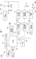
図1は、コントローラ300のブロック図である。この図1を参照して、コントローラ300の基本構成を説明する。
FIG. 1 is a block diagram of the
光電センサ1の基本構成:
光電センサ1は、コントローラ300(図3)と、このコントローラ300に、典型的な光伝搬部材である光ファイバFbで接続された投光ヘッド100(図5)と、コントローラ300に、典型的な光伝搬部材である光ファイバFbで接続された受光ヘッド200(図5)とを含んでいる。
Basic configuration of photoelectric sensor 1 :
The
図1を参照して、コントローラ300は投光部102と受光部202とを備えている。投光部102は所定のパルス光を投光ヘッド100に出力する。投光部102の発光素子104は、投光電源制御回路302から供給される発振パルスによって駆動されて、パルス光を発する。受光部202が受光した光は受光素子204で光電変換され、受光素子増幅回路206、コントローラ300の増幅回路304、A/D変換器306を経て制御部308に送られる。これによって、パルス光に同期した検波が施され、検波信号は更に直流信号等に変換された後、インタフェース部を構成するI/O回路360から、検出結果を表わすON/OFF信号として出力される。
With reference to FIG. 1, the
コントローラ300は投光部102として投光用の発光素子104及びこの発光素子104を駆動するための投光回路106を備える。発光素子104の典型例はLEDである。投光回路106は、投光APC回路108と、モニタPD等のモニタ用受光素子110を備える。投光APC回路108は発光素子104の出力、つまり発光量が所定値となるよう制御する。
The
投光部102のモニタ用受光素子110はモニタ信号増幅回路114に接続されており、モニタラインを介してLED発光量モニタ回路312に受光量を送出する。LED発光量モニタ回路312は、A/D変換器314を介してデジタル信号に変換した受光量信号を制御部308に供給する。制御部308は、モニタ用受光素子110が検出した発光量に基づいて、発光量が所定値となるように投光電源制御回路302を制御し、投光APC回路108の電流量を調整して発光素子104を駆動するフィードバック制御を行う。
The monitor
コントローラ300は受光素子204を駆動するための受光回路208を備える受光素子204は受光素子増幅回路206に接続されており、前述したように、受光素子204で受光した受光量は受光素子増幅回路206で増幅されて、増幅回路304に送出される。コントローラ増幅回路304で増幅されたアナログ信号は、A/D変換器306を介してデジタル信号に変換され、制御部308に入力される。これにより受光素子(フォトダイオードPD)204の受光量を検出し、そして所定のしきい値に基づいて検出の判定を行い、その比較結果を示す検出信号を生成して、最終的にI/O回路360から判定結果を出力する。
The
制御部308には、各種設定値などを記憶するための記憶部326、コントローラ300側の情報を表示するための表示回路328、設定値調整を受け付けるためのユーザインタフェースである操作部362(図2)を接続したスイッチ入力回路330、外部との入出力を行うI/O回路360などが接続されており、これら回路はコントローラ電源回路332によって駆動される。
The
なお,制御部308は,例えば,CPU, FPGA,ASICなどのICから構成される。各種回路(108、114、206、214、302、304、306、312、314、320、328、330、332、360)は,それぞれがICから構成されていてもよいし,各種回路で1つのICで構成されていてもよいし,制御部と各種回路とが1つのICで構成されていてもよい。
The
次に、光電センサ1の調整機能を実現する構成を図2に示すブロック図に基づいて説明する。コントローラ300は、前述した各種制御を行うための制御部308及び設定値などを記憶するための記憶部326と、しきい値や検出値、目標値などを表示するための表示部334と、各種操作や設定を行うための操作部362と、表示部334における表示モードを切り替えるための表示切替部358と、検出結果を出力するための出力部360と、受光部202で受光した受光量のアナログ信号をデジタル信号に変換するためのA/D変換器306とを備える。また制御部308は、表示用変換率調整部336と、しきい値調整部338と、判定部340と、検出値を保持する検出値保持部342と、しきい値を保持するしきい値保持部344とを含む。さらに記憶部326は、しきい値記憶部346と、表示用基準目標値記憶部348と、表示用基準検出値記憶部350と、表示用変換率記憶部352が含まれる。制御部308はCPU等のマイクロプロセッサで構成されている。コントローラ300の操作部362は、表示用基準目標値設定部354と、基準検出値取得部356とを含む。
Next, a configuration for realizing the adjustment function of the
図1、図5を参照して、光電センサ1は、投光部102で発した検出光を光ファイバFbを介して投光ヘッド100に供給する。投光ヘッド100は検出領域に向けて光を出射する。検出領域からの光を受光ヘッド200を介して受け取り、この光は光ファイバFbを介して受光部202に供給される。受光部202で受光した受光量を検出値として判定部340(図2)がしきい値と比較し、その判定結果を出力部360より出力する。具体的には、判定部340(図2)は、入力された検出値のデジタル値をしきい値と比較して、その結果を検出対象物の有無を示す二値信号として出力部360から外部機器へ出力する。
With reference to FIGS. 1 and 5, the
図3はコントローラ300を斜め上方から見た斜視図であり、図3には、DINレール2に4つのコントローラ300を互いに隣り合わせに設置した例が図示されており、そのうちの1台のコントローラ300が上蓋4を開いた状態で図示されている。
FIG. 3 is a perspective view of the
DINレール2に隣接して設置された複数のコントローラ300は、その1つが親機であり、他が子機である。例えば親機の投光が終わると、親機から第1の子機に投光開始の信号が供給され、第1の子機の投光が実行される。この第1の子機の投光が終わると、第1の子機から第2の子機に投光開始の信号が供給され、第2の子機の投光が実行される。以下、第3、第4の子機の投光が順次開始される。
One of the plurality of
図4は光電センサ1の平面図である。図3及び図4を参照して、表示部334は、横並びに配置した2つの4桁7セグメントディスプレイD1、D2で構成され、この2つの4桁7セグメントディスプレイD1、D2を使って検出値(受光量)やしきい値等が表示される。表示部334を液晶ディスプレイなどの平面ディスプレイで構成してもよい。
FIG. 4 is a plan view of the
ディスプレイD1、D2に隣接して、スイング式のアップダウンボタン6、モードボタン8、セットボタン10、プリセットボタン12等が配設されている。
A swing-type up / down
図2に戻って、コントローラ300は表示切替部358を有し、この表示切替部358は上記のモードボタン(Mボタン)8やプリセットボタン12で構成される。モードボタン8やプリセットボタン12を操作することにより、検出値(受光量)及びしきい値をそのまま表示する無変換表示モードと、表示用変換率又は表示用変換式で変換した表示用検出値(表示用受光量)及び表示用しきい値を表示する変換表示モードとを切り替えることができる。
Returning to FIG. 2, the
セットボタン10とアップダウンボタン6とを操作してしきい値を調整することができる。アップダウンボタン6は、また、しきい値その他の数値の変更、選択肢の決定などに使用される。コントローラ300の表示対象、表示態様、表示示切替え操作、表示モード切替えに関してJP特開2006−351380号明細書に詳しく記載されていることから、このJP特開2006−351380号明細書を援用することにより、その説明を省略する。
The threshold value can be adjusted by operating the
以上、透過型光電センサ1について説明したが、反射型の光電センサの構造も実質的に同じであり、本発明は透過型に限定されず、反射型の光電センサにも適用可能である。本発明は、投光ヘッド100及び受光ヘッド200とコントローラ300とを光伝搬部材である光ファイバFbで接続するファイバ型の光電センサに好適に適用されるのは前述した通りである。
Although the transmissive
図5を参照して、受光ヘッド200は、投光ヘッド100からの光を受ける受光筒200aを有する。投光ヘッド100は、検出光を出射する投光筒100aを有し、検出光を検出領域に向けて投光する。受光ヘッド200は検出領域からの光を受け取る。投光ヘッド100と受光ヘッド200の設定において、その相対的な位置決めは光電センサ1の性能を左右する。位置決めは、投光筒100aと受光ヘッド200の受光筒200aとを対面させ、そして、投光筒100aの軸線と受光筒200aの軸線とを整合させることにより行われる。投光ヘッド100と受光ヘッド200とを適正に設置することにより、受光ヘッド200と投光ヘッド100との間をワークWが通過することに伴う遮光の有無によってワークWの「有り」、「無し」を適正に検出することができる。
With reference to FIG. 5, the
表示発光機構:
図1を参照して、受光部202は、発光源としての表示発光素子212を含んでいる。表示発光素子212は典型的にはLEDで構成される。例えば、発光素子104が赤色LEDで構成されているときには、緑色のLEDで表示発光素子212を構成するのがよい。表示発光素子212は、表示発光制御回路214によって点灯が制御され、この表示発光制御回路214は表示発光電源制御回路320によって駆動電力の供給を受ける。
Display light emitting mechanism :
With reference to FIG. 1, the
受光部202で受けた光は,受光素子(PD)204、受光増幅回路206、コントローラ増幅回路304を介して増幅され、A/Dコンバータ306でA/D変換される。制御部308はその信号をもとに,受光量が図25を用いて説明したように,受光量に基づき,表示発光素子212を制御する。受光量に基づき,(a)表示光(可視光)の色、(b)点滅の回数、(c)点滅周期、(d)表示の強弱の周期、(e)複数の表示色の切り替え周期などによって制御することができる。
The light received by the
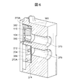
コントローラ300のハード構成(図6〜図9):
図6を参照して、コントローラ300は素子ホルダ368を有し、この素子ホルダ368には、投光部材370と、受光部材372とが収容されている。投光部材370は前述した投光部102を実質的に構成する。受光部材372は前述した受光部202を実質的に構成する。素子ホルダ368は、投光ヘッド100との間の光伝搬部材である光ファイバFbを受け入れる第1挿入穴376と、受光ヘッド200との間の光伝搬部材である光ファイバFbを受け入れる第2挿入穴378とを有している。第1挿入穴376は、投光用の光ファイバを接続する投光用接続部を構成する。また、第2挿入穴378は、受光用の光ファイバを接続する受光用接続部を構成する。第1、第2の挿入穴376、378の中に光ファイバFbの先端部が深く嵌入される。
Hardware configuration of controller 300 (FIGS. 6 to 9) :
With reference to FIG. 6, the
図6と、コントローラ300の縦断面図である図7とを参照して、投光部材370は、発光素子104としてLED、モニタPD等のモニタ用受光素子110、リフレクタ380を含む。モニタ用受光素子110は、発光素子104の発光量を検出する。そして、検出した発光量が所定値となるように発光素子104のフィードバック制御が行われる。
With reference to FIG. 6 and FIG. 7 which is a vertical sectional view of the
受光部材372は、フォトダイオードPDで構成される受光素子204、表示発光素子としてのLED212を含み、表示発光LED212は受光素子204の上に配置されている。すなわち、受光素子204は、その主なる受光面、つまり第2挿入穴378(受光用光ファイバFb)と対面する受光面を有し、表示発行LED212は、この受光素子204の主なる受光面の上に配置されている。図7において、参照符号382は投光用実装基板を示し、参照符号384は受光用実装基板を示す。
The
図7の参照符号386は、第1実施例に含まれる投光部材370A(図6)が設置される投光側空間を示し、参照符号388は受光部材372(図6)が設置される受光側空間を示す。投光側空間386と受光側空間388とは光学的に隔絶されている。投光側空間386と第1挿入穴376(投光側の光ファイバFbを受け入れる穴)との相対位置を説明するための図8を参照して、発光素子104は、その中心が第1挿入穴376の軸線と一致するように位置決めされる。受光側空間388と第2挿入穴378(受光側の光ファイバFbを受け入れる穴)との相対位置を説明するための図9を参照して、受光素子204は、その中心が第2挿入穴378の軸線と一致するように位置決めされる。
図6、図7を参照して、受光素子204は受光用実装基板384に実装されている。そして、受光素子204の上に表示発光素子212が配置され、受光素子204及び表示発光素子212は、受光用光ファイバFbの挿入端と実質的に同軸となるように位置決めされる。したがって、受光側光ファイバFbの挿入端に対して、受光素子204は表示発光素子212に比べて遠い位置に配置されている。換言すれば、受光側光ファイバFbの挿入端に対して、表示発光素子212は受光素子204に比べて接近した位置に配置されている。そして、受光側光ファイバFbを受け入れる第2挿入穴378と受光側空間388との間には、透光部材であるガラス板374が介装されている。受光用光ファイバFbは、その挿入端がガラス板374と当接する位置が正規の挿入組付位置である。
With reference to FIGS. 6 and 7, the
図10は、第2実施例に含まれる受光部材372B及び投光部材370Bを説明するための図である。図10に図示の受光部材372Bは、図6に図示の受光部材372Aの変形例でもある。
FIG. 10 is a diagram for explaining the
受光部材372Bは、フォトダイオードベアチップで構成された受光素子204を含み、また、発光源としてLEDベアチップで構成された表示発光素子212を含んでいる。そして、フォトダイオードベアチップは受光用実装基板384に実装されている。
The
すなわち、受光用実装基板384を位置決めすることにより、受光素子204を構成するフォトダイオードベアチップが受光用光ファイバFbの挿入端の軸線上にセンタリングされた状態で位置決めされる。受光素子204は受光用実装基板384に搭載されている。勿論、受光面204aは受光用光ファイバFbに対面した状態で位置決めされている。そして、受光用光ファイバFbに差し向けられている受光面204aの上に表示発光素子212が搭載されている。更に、表示発光素子212と受光素子204は共通の断面台形の透明のモールド樹脂Rで包囲されている。すなわち、受光用実装基板384側にフォトダイオードベアチップ(受光素子204)が配設され、受光用光ファイバFbの挿入端側にLEDベアチップ(表示発光素子212)が配設され、これらは共通の透明のモールド樹脂Rで包囲されている。モールド樹脂Rの外面に金属蒸着する等、光を反射する材料でモールド樹脂Rを包囲するのがよい。受光用光ファイバFbの挿入端はモールド樹脂Rに当接した状態で第2の挿入穴378に固定される。第2の挿入穴378に挿入される受光用光ファイバFbは、その挿入端がモールド樹脂Rと当接する位置が正規の挿入組付位置である。
That is, by positioning the light
図10から分かるように、受光素子204のフォトダイオードベアチップの受光面204aは、表示発光素子212のLEDベアチップよりも大きい。
As can be seen from FIG. 10, the
受光素子204の上に搭載された表示発光素子212は透明のモールド樹脂Rによって受光用光ファイバFbの挿入端から離間した状態に位置決めされる。図10において、矢印は受光用光ファイバFbから受光部材372Bの中に入る検出光を示す。この検出光は、受光用光ファイバFbの挿入端から末広がりの状態で受光部材372Bの中に入る。受光エリアをドットで図示してある。この検出光は、受光素子204の受光面204aのうち表示発光素子212が占める部分を除く部分で受光されることになる。すなわち、受光素子204の受光面204aの面積に比べて表示発光素子212が占める面積は相当に小さく、受光面204aの中心部分に表示発光素子212が位置決めされている。受光素子204は、その中心部分の外周部分で受光することができる。
The display
受光素子204の上に載置された状態の表示発光素子212は、光ファイバFbの挿入端に近づいた状態で位置決めされることになる。したがって、表示発光素子212の光量が比較的少なくても、光ファイバFbに入る光量が多いため、光ファイバFbの先端つまり受光ヘッド200で強く光らせることができる。換言すれば、受光ヘッド200で光らせる程度が同じであれば、光表示発光素子212を光ファイバFbの挿入端に近づければ近づけるほど、光表示発光素子212が発する光量は少なくてよい。
The display
コントローラ300は、投光部材370Bとして、発光素子104としてのLEDと、モニタPD等のモニタ用受光素子110とに加えて、発光源としての光表示発光素子120を含んでいてもよい。これらはコントローラ300の中で横並びに位置決めされている投光用実装基板382に実装されている。モニタ用受光素子110は、前述したように、発光素子104の発光量を検出する。そして、検出した発光量は、これが所定値となるように発光素子104をフィードバック制御するのに用いられる。
The
図10から良く分かるように、モニタ用受光素子110は、受光部材372Bから最も又は極力遠ざかる位置に配置されている。すなわち、モニタ用受光素子110は、受光部材372Bとは反対側に配置されている。
As can be clearly seen from FIG. 10, the monitor
この光表示発光素子120は典型的にはLEDで構成され、このLEDは、発光素子104のLEDと同じ色のLEDであってもよいが、異なる色のLEDであるのがよい。具体的には、発光素子104のLEDが赤であれば、光表示発光素子120のLEDは緑であるのがよい。
The light display
投光部材370Bに含まれる光表示発光素子120の色は、受光部材372Bに含まれる表示発光素子212の色と同じであってもよいし、異なっていてもよい。異なる色を採用することにより、投光ヘッド100と受光ヘッド200の区別が容易になる。
The color of the light display
発光素子104のLEDはベアチップで構成され、光表示発光素子120のLEDもベアチップで構成されている。投光用光ファイバFbの挿入端に対して、発光素子104を構成するLEDベアチップと、光表示発光素子120を構成するLEDベアチップとは互いに横並びの状態で位置決めされている。そして、発光素子104と光表示発光素子120とは、共通の断面台形の透明のモールド樹脂Rで包囲されている。投光用光ファイバFbの挿入端はモールド樹脂Rに当接した状態で第1の挿入穴376に固定される。すなわち、投光用光ファイバFbは、その挿入端がモールド樹脂Rと当接する位置が正規の挿入組付位置である。
The LED of the
図11は、第3実施例に含まれる受光部材372Cを説明するための図である。図11に図示の受光部材372Cは、図10に図示の受光部材372Bの変形例でもある。図11に図示の受光部材372Cは3層構造となっている。すなわち、受光部材372はフォトダイオードベアチップで構成された受光素子204を有し、この受光素子204は受光用実装基板384に実装されている。そして、この受光素子204と、その上方に位置するLEDベアチップで構成された表示発光素子212との間に、波長選択性の光吸収能力を有するフィルタ部材390が搭載されている。フィルタ部材390は、受光素子204の受光面204aと同じ面積を有していても良いし、表示発光素子212が当接する部位及びその周辺に限定した大きさを有していてもよい。また、フィルタ部材390は、受光面204aよりも大きな面積を有していてもよい。フィルタ部材390はフィルム塗膜に比べて厚みを有し、例えば赤色ガラスなどの色ガラスや、カラーコーティングした透明部材で構成される。このフィルタ部材390によって、表示発光素子212が発する光が受光素子204に対して悪影響を及ぼす程度を低減することができる。すなわち、色ガラスや、カラーコーティングした透明部材などのフィルタ部材390は、表示発光素子212が発する可視光(表示光)が受光素子204に入光する、その光の量を低減する手段を構成している。
FIG. 11 is a diagram for explaining the
受光素子204、フィルタ部材390、表示発光素子212は共通の断面台形の透明のモールド樹脂Rで包囲されている。モールド樹脂Rの形状は、図13などを参照して説明する砲弾型であってもよい。受光用光ファイバFbの挿入端はモールド樹脂Rに当接した状態で第2の挿入穴378に固定される。すなわち、受光用光ファイバFbは、その挿入端がモールド樹脂Rと当接する位置が正規の挿入組付位置である。
The
図11に図示の受光部材372Cの変形例として、共通のモールド樹脂Rの代わりに、図6を参照して説明したように、受光側の光ファイバFbを受け入れる第2挿入穴378と受光側空間388との間に、透光部材であるガラス板374を介装してもよい。
As a modification of the
図12は、第4実施例に含まれる受光部材372Dを説明するための図である。この第4実施例に含まれる受光部材372Dは、上述した図11の受光部材372Cの変形例でもある。受光部材372Dは、厚さを有する上記のフィルタ部材390に代えて、波長選択性の光吸収能力又は光反射能力を有するフィルム又はカラーコーティングなどの薄膜392を有する。この薄膜392は、受光素子204の受光面204aの全域に配置してもよいし、表示発光素子212が当接する部位及びその周辺に限定して配置してもよい。
FIG. 12 is a diagram for explaining the
図12に図示の受光部材372Dの変形例として、共通のモールド樹脂Rの代わりに、図6を参照して説明したように、受光側の光ファイバFbを受け入れる第2挿入穴378と受光側空間388との間に、透光部材であるガラス板374を介装してもよいのは、上記の図11に図示の受光部材372Cと同じである。
As a modification of the
図13は、第5実施例に含まれる受光部材372Eを説明するための図である。図13に図示の受光部材372Eは、受光用実装基板384に実装されLEDチップからなる表示発光素子212を有し、また、リードフレーム230によって表示発光素子212の上方に間隔を隔てて位置決めされた受光素子204を有し、受光素子204はフォトダイオードベアチップで構成されている。受光素子204及び表示発光素子212は、受光用光ファイバFbの挿入端と実質的に同軸となるように位置決めされる。図中、参照符号232はワイヤを示す。リードフレーム230及び受光素子204は砲弾型の成形された透明のモールド樹脂Rで包囲されている。受光用光ファイバFbの挿入端は、砲弾型のモールド樹脂Rに当接した状態で第2の挿入穴378に固定される。すなわち、受光用光ファイバFbは、その挿入端が砲弾型のモールド樹脂Rと当接する位置が正規の挿入組付位置である。
FIG. 13 is a diagram for explaining the
砲弾型のモールド樹脂Rの底面に上記LEDチップからなる表示発光素子212を接着剤で接着するのがよい。もちろん、接着剤は光透過性の材料で構成するのがよい。
It is preferable to adhere the display
表示発光素子212が発する光は、砲弾型のモールド樹脂Rの中を通って受光用光ファイバFbの中に誘導される。
The light emitted by the display
図13に図示の受光部材372Eによれば、受光用光ファイバFbの挿入端に対して、受光素子204は表示発光素子212に比べて接近した状態に配置することができるだけでなく、受光素子204を受光用光ファイバFbの挿入端に極力近づけた位置に配置することができるため、受光素子204の高い受光性能を確保することができる。
According to the
受光素子204の下面や側面に塗布するなどして遮光材料や反射材料を配置してもよい。また、砲弾型のモールド樹脂Rの外面に金属蒸着する等、光を反射する材料でモールド樹脂Rを包囲するのがよい。
A light-shielding material or a reflective material may be arranged by applying the light-receiving
図14は、第6実施例に含まれる受光部材372Fを説明するための図である。この図14に図示の受光部材372Fは、上記図13に図示の受光部材372Eの変形例でもある。図13に図示の受光部材372Eでは、LEDチップからなる表示発光素子212を受光用実装基板384に実装したが、図14に図示の受光部材372Fでは、表示発光素子212と実装基板384との間に放熱板394が介装されている。また、LEDチップからなる表示発光素子212を樹脂モールドRで包囲してもよい。放熱板394の代わりに、ベアチップで構成された表示発光素子212を伝熱性接着材を使って実装基板384に固定することで放熱性を問題を解消してもよい。
FIG. 14 is a diagram for explaining the
図15は、第7実施例に含まれる受光部材372Gを説明するための図である。この図15に図示の受光部材372Gは、上記図13に図示の受光部材372Eの変形例又は図14に図示の受光部材372Fの変形例でもある。図13、図14に図示の受光部材372E、372Fは、表示発光素子212の上方に位置決めされた受光素子204を砲弾型の樹脂モールドRで包囲する構成が採用されているが、図15に図示の受光部材372Gは、表示発光素子212の上方に外乱光除去フィルタ364が配置され、この外乱光除去フィルタ364は表示発光素子212と共通の樹脂モールドRによって包囲されている。図15に図示の受光部材372Gは、図14の受光部材372Fの変形例として描かれているが、図13に図示の受光部材372Eに外乱光除去フィルタ364を加える構成を有していてもよい。
FIG. 15 is a diagram for explaining the
受光用光ファイバFbの挿入端と受光素子204と間に外乱光除去フィルタ364が介在しているため、受光素子204に対する外乱光の影響を抑えることができる。
Since the disturbance
図16は、第8実施例に含まれる受光部材372Hを説明するための図である。この図16に図示の受光部材372Hは、受光用実装基板384の上方に追加の実装基板384aを有し、この追加の実装基板384aの一方側の面つまり受光用実装基板384と対面する側の面にLEDベアチップからなる表示発光素子212が実装されている。
FIG. 16 is a diagram for explaining the
追加の実装基板384aの他方側の面つまり受光用光ファイバFbの挿入端と対面する側の面にはフォトダイオードベアチップが実装されている。このフォトダイオードベアチップは受光素子204を構成する。追加の実装基板384aに実装されたLEDベアチップ212及びフォトダイオードベアチップ204は共にモールド樹脂Rで包囲されているのが好ましい。変形例として、追加の実装基板384aのフォトダイオードベアチップ204を砲弾型のモールド樹脂Rで包囲してもよい。なお、図16は、受光素子204、実装基板384a、LEDベアチップ212などの配置関係を説明するための図であるので、各要素に通じる電気配線は、線図の錯綜を避けるために、その図示を省いてある。
A photodiode bare chip is mounted on the other side surface of the additional mounting
受光側の光ファイバFbを受け入れる第2挿入穴378と受光側空間388との間には、透光部材であるガラス板374が介装されている。受光用光ファイバFbは、その挿入端がガラス板374と当接する位置が正規の挿入組付位置である。
A
図17は、第9実施例に含まれる受光部材372Iを説明するための図である。図17の受光部材372Iは、フォトダイオードベアチップで構成された受光素子204と、LEDベアチップからなる表示発光素子212とが横並びに位置決めされた状態で受光用実装基板384に実装されている。そして、受光素子204は、その中心が第2挿入穴378の軸線と一致するように位置決めされている。
FIG. 17 is a diagram for explaining the light receiving member 372I included in the ninth embodiment. The light receiving member 372I of FIG. 17 is mounted on the light
受光側光ファイバFbを受け入れる第2挿入穴378と受光側空間388との間には、透光部材であるガラス板374が介装されている。受光用光ファイバFbは、その挿入端がガラス板374と当接する位置が正規の挿入組付位置である。表示発光素子212の光は、受光素子204と共通のガラス板(透光部材)374を通じて受光用光ファイバFbに受け入れられる。
A
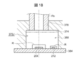
図18は、第10実施例に含まれる受光部材372Jを説明するための図である。この図18の受光部材372Jは、図17の受光部材372Iの変形例でもある。図17の受光部材372Iでは、受光素子204がフォトダイオードベアチップで構成され、また、表示発光素子212がLEDベアチップで構成されているが、図18の受光部材372Jにあっては、モールド樹脂Rで包囲されたフォトダイオードベアチップで受光素子204が構成され、また、モールド樹脂Rで包囲されたLEDベアチップで表示発光素子212が構成されている。勿論、フォトダイオードベアチップ又はLEDベアチップの少なくともいずれか一方がモールド樹脂Rで包囲されていてもよい。
FIG. 18 is a diagram for explaining the
図19は、第11実施例に含まれる受光部材372Kを説明するための図である。この図19の受光部材372Kは、図18の受光部材372Jの変形例でもある。上述した図18の受光部材372Jでは、フォトダイオードベアチップからなる受光素子204が受光用実装基板384に実装されているが、図19の受光部材372Kでは、リードフレーム230によってフォトダイオードベアチップが実装基板384から上方に離間して位置決めされている。これにより、受光素子204を受光側光ファイバFbに接近した状態で配置することができる。
FIG. 19 is a diagram for explaining the
図20は、第12実施例に含まれる受光部材372Lを説明するための図である。この図20の受光部材372Lは、図19の受光部材372Kの変形例でもある。図19の受光部材372Kでは、受光側光ファイバFbを受け入れる第2挿入穴378と受光側空間388との間にガラス板374が介装されているが、この図20の受光部材372Lでは、リードフレーム230を備えたフォトダイオードベアチップが砲弾型のモールド樹脂Rで包囲されている。ここに、受光用光ファイバFbは、その挿入端が砲弾型のモールド樹脂Rと当接する位置が正規の挿入組付位置である。
FIG. 20 is a diagram for explaining the
図21は、第13実施例に含まれる受光部材372Mを説明するための図である。この図21の受光部材372Mは、受光用実装基板384の上方に離間して位置する追加の実装基板384aを有する。この追加の実装基板384aは台座396によって支持されている。そして、この追加の実装基板384aにフォトダイオードベアチップが実装されている。このフォトダイオードベアチップは受光素子204を構成している。受光素子204は、その中心が第2挿入穴378つまり受光用光ファイバFbの挿入端の軸線と一致するように位置決めされる。
FIG. 21 is a diagram for explaining the
フォトダイオードベアチップを実装した追加の実装基板384aの周囲において、受光用実装基板384には、表示発光素子212を構成するLEDベアチップ212が実装されている。この表示発光素子212は、単数であってもよいが、複数であってもよい。図22は、図21に対応した平面図である。図22において、4つの表示発光素子212が、発光素子204の周囲に等間隔且つ第2挿入穴378の軸線から等間隔に配置されている。
Around the additional mounting
この4つの表示発光素子212は、全て同じ色のLEDで構成してもよいし、異なる色のLEDで構成してもよい。異なる色のLEDで構成することにより、電源を供給するLEDの組み合わせを変えることにより、混色した様々な色の光を受光用光ファイバFbに供給することができ、様々な色を使って異なる情報を表示することができる。
The four display
上述した複数の実施例に含まれる受光部材は、受光素子204だけでなく、表示発光素子212を含む。このことに伴って、受光素子204は、これが対の投光ヘッド100から届いた検出光であるか、表示発光素子212の表示光(可視光)であるかを区別できない。投光ヘッド100の検出光と表示発光素子212の表示光(可視光)とを区別可能にする又は表示発光素子212の表示光が受光素子204に入光する、その光の量を低減する手法を講じるのが好ましい。
The light receiving member included in the plurality of examples described above includes not only the
具体的には、波長を異ならせる、発光タイミングを異ならせる、発光周波数を異ならせる等の手段を講じることにより、光の波長的に、発光タイミング的に、発光周波数的に分離もしくは光の波長的な分離と他のどちらを組み合わせて実施するのがよい。波長を異ならせる手段は、図11、図12を参照して説明したとおり、物理的なフィルタを設けるのがよい。 Specifically, by taking measures such as different wavelengths, different emission timings, and different emission frequencies, the light is separated in terms of wavelength, emission timing, emission frequency, or light wavelength. It is better to carry out a combination of simple separation and others. As a means for making the wavelengths different, it is preferable to provide a physical filter as described with reference to FIGS. 11 and 12.
図23は、発光タイミングを異ならせる例を説明するための図である。発光素子104の隣接する2つの検出用発光パルスの間に表示発光素子212を発光させる。図23には、この表示発光素子212を発光パルスにハッチングを付して識別してある。
FIG. 23 is a diagram for explaining an example in which the light emission timings are different. The display
受光素子110の検出タイミングをT1、T2、T3と付すと、この検出タイミングT1、T2、T3の中間で表示発光素子212が光るため、受光素子110は正規に検出用発光パルスを受け取ることができる。
When the detection timing of the
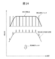
図24は発光周波数的に分離する方法を例示的に説明するための図である。発光素子104の検出用発光パルスは所定のタイミングでON/OFFを繰り返す。これに表示発光素子212の光が重畳しても検出用発光パルスの波形が維持された状態で受光素子110が光を受け取る。このことから受光素子110の出力波形を周波数フィルタ(ハイパス)でフィルタリングすることにより、発光素子104が発する検出光だけを取り出すことができる。
FIG. 24 is a diagram for exemplifying a method of separating in terms of emission frequency. The light emitting pulse for detection of the
図24を参照したフィルタリングでは表示発光素子212の発光波形の周波数を下げることにより、検出と表示で使用する周波数領域を区分したが、図24の例とは逆に、表示発光素子212の発光波形の周波数を挙げて周波数領域を区分するようにしてもよい。
In the filtering with reference to FIG. 24, the frequency range used for detection and display was divided by lowering the frequency of the emission waveform of the display
Fb 光ファイバ(光伝搬部材)
100 投光ヘッド
102 投光部
104 発光素子
120 第2の表示発光素子
200 受光ヘッド
202 受光部
204 受光素子
212 第1の表示発光素子
230 リードフレーム
300 コントローラ
372 受光部材
374 ガラス板(透光部材)
376 第1挿入穴(投光用接続部)
378 第2挿入穴(受光用接続部)
382 投光用実装基板
384 受光用実装基板
370 投光部材
390 フィルタ部材
392 薄膜
R 樹脂モールド(透光部材)
Fb optical fiber (light propagation member)
100
376 First insertion hole (light projection connection)
378 Second insertion hole (light receiving connection)
382 Light-emitting mounting
Claims (15)
前記検出領域からの検出光を受光する受光素子と、
前記発光素子に光結合される投光用光伝搬部材が接続される投光用接続部と、
前記受光素子に光結合される受光用光伝搬部材が接続される受光用接続部と、
前記受光素子で生成された受光信号としきい値とを比較して比較結果を示す検出信号を生成する信号生成部と、
前記受光用接続部に光結合され且つ可視光を発する第1の表示用発光素子と、
前記受光用接続部と前記受光素子との間に位置し、かつ、前記第1の表示用発光素子の発した可視光が前記受光用接続部に入光するにあたり通過し、前記発光素子の発した検出光が前記受光用接続部を介して前記受光素子に入光するにあたり通過する透光部材と、
前記第1の表示用発光素子が発する可視光が前記受光素子に入光する、その光の量を低減する低減手段と、を有する光電センサ。 A light emitting element that projects the detection light toward the detection area,
A light receiving element that receives the detection light from the detection region and
A light projecting connection portion to which a light projecting light propagating member optically coupled to the light emitting element is connected.
A light receiving connection portion to which a light receiving light propagation member optically coupled to the light receiving element is connected,
A signal generation unit that compares a light receiving signal generated by the light receiving element with a threshold value and generates a detection signal indicating a comparison result, and a signal generation unit.
A first display light-emitting elements are optically coupled and emit visible light in the light receiving connecting portion,
It is located between the light receiving connection portion and the light receiving element, and the visible light emitted by the first display light emitting element passes through when it enters the light receiving connection portion, and the light emitting element emits light. A translucent member through which the detected light enters the light receiving element via the light receiving connection portion.
A photoelectric sensor having a reduction means for reducing the amount of visible light emitted by the first display light emitting element and entering the light receiving element.
該受光素子の上に前記第1の表示用発光素子が配置され、
該第1の表示用発光素子と前記受光素子との間に前記フィルタが介装されている、請求項4に記載の光電センサ。 The light receiving element is mounted on a light receiving mounting substrate and is mounted on a light receiving mounting substrate.
The first display light emitting element is arranged on the light receiving element, and the first display light emitting element is arranged.
The photoelectric sensor according to claim 4 , wherein the filter is interposed between the first display light emitting element and the light receiving element.
該モールド樹脂に前記フィルタが設けられている、請求項4〜6のいずれか一項に記載の光電センサ。 The light receiving element is composed of a photodiode bare chip and a mold resin surrounding the photodiode bare chip.
The photoelectric sensor according to any one of claims 4 to 6 , wherein the filter is provided on the mold resin.
前記第1の表示用発光素子が発した前記可視光が前記透光部材を通じて前記受光用光伝搬部材に入ると共に前記フィルタを通じて前記受光素子に受光される、請求項4〜6のいずれか一項に記載の光電センサ。 The detected light enters the light receiving element from the light receiving light propagating member through the light transmitting member.
Any one of claims 4 to 6 , wherein the visible light emitted by the first display light emitting element enters the light receiving light propagation member through the light transmitting member and is received by the light receiving element through the filter. The photoelectric sensor described in.
該第2の表示用発光素子が発した表示光が前記投光用光伝搬部材を通って該投光用光伝搬部材の先端を光らせる、請求項1〜11のいずれか一項に記載の光電センサ。 The light emitting unit having the light emitting element and the light projecting connection portion includes a light projecting element that emits detection light and a second display light emitting element that is photocoupled to the light projecting light propagating member and emits visible light. And have more
The photoelectric light according to any one of claims 1 to 11 , wherein the display light emitted by the second display light emitting element illuminates the tip of the light projecting light propagating member through the light projecting light propagating member. Sensor.
該素子ホルダが、
前記投光用光伝搬部材が挿入される投光用挿入穴と、
前記受光用光伝搬部材が挿入される受光用挿入穴と、
前記投光部を収容する投光部収容部と、
前記受光部を収容する受光部収容部と、を備え、
前記透光部材と前記第1の表示用発光素子とは、前記受光部収容部に収容されている、請求項1〜13のいずれか一項に記載の光電センサ。 It also has an element holder
The element holder
A light projection insertion hole into which the light projection light propagation member is inserted,
A light receiving insertion hole into which the light receiving light propagation member is inserted, and a light receiving insertion hole.
A light projecting unit accommodating unit for accommodating the light projecting unit and
A light receiving unit accommodating portion for accommodating the light receiving unit is provided.
Wherein the translucent member and the first display light-emitting device, wherein are housed in the light-receiving portion accommodating portion, the photoelectric sensor according to any one of claims 1 to 13.
前記検出領域からの検出光を受光する受光素子と、
前記発光素子に光結合される投光用光伝搬部材が接続される投光用接続部と、
前記受光素子に光結合される受光用光伝搬部材が接続される受光用接続部と、
前記受光素子で生成された受光信号としきい値とを比較して比較結果を示す検出信号を生成する信号生成部と、
前記投光用接続部に光結合され且つ可視光を発する第2の表示用発光素子と、
前記投光用接続部と前記発光素子との間に位置し、かつ、前記第2の表示用発光素子の発した可視光が前記投光用接続部に入光するにあたり通過し、前記発光素子の発した検出光が前記受光用接続部を介して前記受光素子に入光するにあたり通過する透光部材と、
前記第2の表示用発光素子が発する可視光が前記受光素子に入光する、その光の量を低減する低減手段と、を有する光電センサ。
A light emitting element that projects the detection light toward the detection area,
A light receiving element that receives the detection light from the detection region and
A light projecting connection portion to which a light projecting light propagating member optically coupled to the light emitting element is connected.
A light receiving connection portion to which a light receiving light propagation member optically coupled to the light receiving element is connected,
A signal generation unit that compares a light receiving signal generated by the light receiving element with a threshold value and generates a detection signal indicating a comparison result, and a signal generation unit.
A second display light-emitting elements are optically coupled and emit visible light in the light projecting connecting portion,
It is located between the light emitting connection portion and the light emitting element, and the visible light emitted by the second display light emitting element passes through when entering the light emitting connecting portion, and the light emitting element A translucent member that passes when the detection light emitted by the light enters the light receiving element via the light receiving connection portion.
A photoelectric sensor having a reduction means for reducing the amount of visible light emitted by the second display light emitting element, which enters the light receiving element.
Priority Applications (1)
| Application Number | Priority Date | Filing Date | Title |
|---|---|---|---|
| JP2017066458A JP6904750B2 (en) | 2017-03-29 | 2017-03-29 | Photoelectric sensor |
Applications Claiming Priority (1)
| Application Number | Priority Date | Filing Date | Title |
|---|---|---|---|
| JP2017066458A JP6904750B2 (en) | 2017-03-29 | 2017-03-29 | Photoelectric sensor |
Publications (3)
| Publication Number | Publication Date |
|---|---|
| JP2018170625A JP2018170625A (en) | 2018-11-01 |
| JP2018170625A5 JP2018170625A5 (en) | 2020-05-21 |
| JP6904750B2 true JP6904750B2 (en) | 2021-07-21 |
Family
ID=64020485
Family Applications (1)
| Application Number | Title | Priority Date | Filing Date |
|---|---|---|---|
| JP2017066458A Active JP6904750B2 (en) | 2017-03-29 | 2017-03-29 | Photoelectric sensor |
Country Status (1)
| Country | Link |
|---|---|
| JP (1) | JP6904750B2 (en) |
Families Citing this family (1)
| Publication number | Priority date | Publication date | Assignee | Title |
|---|---|---|---|---|
| CN114137269A (en) * | 2021-11-24 | 2022-03-04 | 广西电网有限责任公司 | Bluetooth photoelectric head and method for reading and writing multi-protocol electric energy meter |
Family Cites Families (7)
| Publication number | Priority date | Publication date | Assignee | Title |
|---|---|---|---|---|
| JPS57107527A (en) * | 1980-12-25 | 1982-07-05 | Matsushita Electric Works Ltd | Operation display unit for optical fiber type photoelectric switch |
| JPH10173207A (en) * | 1996-10-11 | 1998-06-26 | Sharp Corp | Optical transmission-reception module |
| JP3774335B2 (en) * | 1999-06-23 | 2006-05-10 | シャープ株式会社 | Optical transceiver module and single-core bidirectional optical communication system using the same |
| JP2002148117A (en) * | 2000-11-14 | 2002-05-22 | Yamatake Corp | Optical sensor |
| JP2003084173A (en) * | 2001-09-10 | 2003-03-19 | Citizen Electronics Co Ltd | Bidirectional optical transmission device |
| JP2008091173A (en) * | 2006-09-29 | 2008-04-17 | Sunx Ltd | Photoelectric sensor |
| JP2014135473A (en) * | 2012-12-11 | 2014-07-24 | Renesas Electronics Corp | Optical coupling element |
-
2017
- 2017-03-29 JP JP2017066458A patent/JP6904750B2/en active Active
Also Published As
| Publication number | Publication date |
|---|---|
| JP2018170625A (en) | 2018-11-01 |
Similar Documents
| Publication | Publication Date | Title |
|---|---|---|
| EP3258301B1 (en) | Optical module with status indicator | |
| CN106448029B (en) | Smoke detector and light Smoke Detection unit for smoke detector | |
| JP4720904B2 (en) | LED lighting fixtures | |
| RU2416811C2 (en) | Light-emitting diode illumination device | |
| JP4782965B2 (en) | Lighting device | |
| JP2013065544A (en) | Led lamp | |
| US20150180202A1 (en) | Solid-State Lighting Device | |
| US10094469B2 (en) | Apparatus for optoelectronically detecting a selector lever position, selector lever apparatus, method for producing an apparatus and method for optoelectronically detecting a selector lever position wherein predetermined light intensities or filtered wavelengths are assigned to predetermined positions | |
| JP6917748B2 (en) | Photoelectric sensor | |
| JP6996860B2 (en) | Photoelectric sensor | |
| JP2006310307A (en) | Light source of lcd backlight display | |
| CA3029286C (en) | Led shielding and monitoring system and wayside led signals | |
| JP6904750B2 (en) | Photoelectric sensor | |
| JP2010501976A (en) | Lighting device | |
| JP2010152304A (en) | Illumination light display device | |
| JP4141169B2 (en) | area sensor | |
| CN107636384B (en) | Signal generating device for a command and/or signal instrument | |
| KR20150119488A (en) | Electronic device with shared light guide | |
| JP2014041726A (en) | Lighting system, wiring duct, and power feeding unit | |
| KR101131462B1 (en) | decoration tile based on optical fiber and LED | |
| JP2012169245A (en) | Led unit and lighting fixture | |
| JP4899527B2 (en) | LED lighting device | |
| JP2005227121A (en) | Countermeasures for preventing mutual interference in photoelectric switch | |
| CN211952330U (en) | Multi-wavelength LED light source | |
| JP2012114028A (en) | Lighting apparatus |
Legal Events
| Date | Code | Title | Description |
|---|---|---|---|
| A521 | Request for written amendment filed |
Free format text: JAPANESE INTERMEDIATE CODE: A523 Effective date: 20200326 |
|
| A621 | Written request for application examination |
Free format text: JAPANESE INTERMEDIATE CODE: A621 Effective date: 20200326 |
|
| A977 | Report on retrieval |
Free format text: JAPANESE INTERMEDIATE CODE: A971007 Effective date: 20210224 |
|
| A131 | Notification of reasons for refusal |
Free format text: JAPANESE INTERMEDIATE CODE: A131 Effective date: 20210302 |
|
| A521 | Request for written amendment filed |
Free format text: JAPANESE INTERMEDIATE CODE: A523 Effective date: 20210427 |
|
| TRDD | Decision of grant or rejection written | ||
| A01 | Written decision to grant a patent or to grant a registration (utility model) |
Free format text: JAPANESE INTERMEDIATE CODE: A01 Effective date: 20210601 |
|
| A61 | First payment of annual fees (during grant procedure) |
Free format text: JAPANESE INTERMEDIATE CODE: A61 Effective date: 20210624 |
|
| R150 | Certificate of patent or registration of utility model |
Ref document number: 6904750 Country of ref document: JP Free format text: JAPANESE INTERMEDIATE CODE: R150 |
|
| R250 | Receipt of annual fees |
Free format text: JAPANESE INTERMEDIATE CODE: R250 |