JP6903262B2 - How to repair equipment parts used in semiconductor processing - Google Patents
How to repair equipment parts used in semiconductor processing Download PDFInfo
- Publication number
- JP6903262B2 JP6903262B2 JP2018508613A JP2018508613A JP6903262B2 JP 6903262 B2 JP6903262 B2 JP 6903262B2 JP 2018508613 A JP2018508613 A JP 2018508613A JP 2018508613 A JP2018508613 A JP 2018508613A JP 6903262 B2 JP6903262 B2 JP 6903262B2
- Authority
- JP
- Japan
- Prior art keywords
- layer
- ceramic
- brazing
- joint
- aluminum
- Prior art date
- Legal status (The legal status is an assumption and is not a legal conclusion. Google has not performed a legal analysis and makes no representation as to the accuracy of the status listed.)
- Active
Links
Images


Classifications
-
- B—PERFORMING OPERATIONS; TRANSPORTING
- B23—MACHINE TOOLS; METAL-WORKING NOT OTHERWISE PROVIDED FOR
- B23P—METAL-WORKING NOT OTHERWISE PROVIDED FOR; COMBINED OPERATIONS; UNIVERSAL MACHINE TOOLS
- B23P6/00—Restoring or reconditioning objects
-
- B—PERFORMING OPERATIONS; TRANSPORTING
- B23—MACHINE TOOLS; METAL-WORKING NOT OTHERWISE PROVIDED FOR
- B23K—SOLDERING OR UNSOLDERING; WELDING; CLADDING OR PLATING BY SOLDERING OR WELDING; CUTTING BY APPLYING HEAT LOCALLY, e.g. FLAME CUTTING; WORKING BY LASER BEAM
- B23K1/00—Soldering, e.g. brazing, or unsoldering
- B23K1/0008—Soldering, e.g. brazing, or unsoldering specially adapted for particular articles or work
-
- B—PERFORMING OPERATIONS; TRANSPORTING
- B23—MACHINE TOOLS; METAL-WORKING NOT OTHERWISE PROVIDED FOR
- B23K—SOLDERING OR UNSOLDERING; WELDING; CLADDING OR PLATING BY SOLDERING OR WELDING; CUTTING BY APPLYING HEAT LOCALLY, e.g. FLAME CUTTING; WORKING BY LASER BEAM
- B23K1/00—Soldering, e.g. brazing, or unsoldering
- B23K1/19—Soldering, e.g. brazing, or unsoldering taking account of the properties of the materials to be soldered
-
- B—PERFORMING OPERATIONS; TRANSPORTING
- B23—MACHINE TOOLS; METAL-WORKING NOT OTHERWISE PROVIDED FOR
- B23K—SOLDERING OR UNSOLDERING; WELDING; CLADDING OR PLATING BY SOLDERING OR WELDING; CUTTING BY APPLYING HEAT LOCALLY, e.g. FLAME CUTTING; WORKING BY LASER BEAM
- B23K35/00—Rods, electrodes, materials, or media, for use in soldering, welding, or cutting
- B23K35/02—Rods, electrodes, materials, or media, for use in soldering, welding, or cutting characterised by mechanical features, e.g. shape
- B23K35/0222—Rods, electrodes, materials, or media, for use in soldering, welding, or cutting characterised by mechanical features, e.g. shape for use in soldering, brazing
- B23K35/0233—Sheets, foils
-
- B—PERFORMING OPERATIONS; TRANSPORTING
- B23—MACHINE TOOLS; METAL-WORKING NOT OTHERWISE PROVIDED FOR
- B23K—SOLDERING OR UNSOLDERING; WELDING; CLADDING OR PLATING BY SOLDERING OR WELDING; CUTTING BY APPLYING HEAT LOCALLY, e.g. FLAME CUTTING; WORKING BY LASER BEAM
- B23K35/00—Rods, electrodes, materials, or media, for use in soldering, welding, or cutting
- B23K35/02—Rods, electrodes, materials, or media, for use in soldering, welding, or cutting characterised by mechanical features, e.g. shape
- B23K35/0222—Rods, electrodes, materials, or media, for use in soldering, welding, or cutting characterised by mechanical features, e.g. shape for use in soldering, brazing
- B23K35/0244—Powders, particles or spheres; Preforms made therefrom
-
- B—PERFORMING OPERATIONS; TRANSPORTING
- B23—MACHINE TOOLS; METAL-WORKING NOT OTHERWISE PROVIDED FOR
- B23K—SOLDERING OR UNSOLDERING; WELDING; CLADDING OR PLATING BY SOLDERING OR WELDING; CUTTING BY APPLYING HEAT LOCALLY, e.g. FLAME CUTTING; WORKING BY LASER BEAM
- B23K35/00—Rods, electrodes, materials, or media, for use in soldering, welding, or cutting
- B23K35/22—Rods, electrodes, materials, or media, for use in soldering, welding, or cutting characterised by the composition or nature of the material
- B23K35/24—Selection of soldering or welding materials proper
- B23K35/28—Selection of soldering or welding materials proper with the principal constituent melting at less than 950 degrees C
- B23K35/286—Al as the principal constituent
-
- C—CHEMISTRY; METALLURGY
- C04—CEMENTS; CONCRETE; ARTIFICIAL STONE; CERAMICS; REFRACTORIES
- C04B—LIME, MAGNESIA; SLAG; CEMENTS; COMPOSITIONS THEREOF, e.g. MORTARS, CONCRETE OR LIKE BUILDING MATERIALS; ARTIFICIAL STONE; CERAMICS; REFRACTORIES; TREATMENT OF NATURAL STONE
- C04B37/00—Joining burned ceramic articles with other burned ceramic articles or other articles by heating
- C04B37/003—Joining burned ceramic articles with other burned ceramic articles or other articles by heating by means of an interlayer consisting of a combination of materials selected from glass, or ceramic material with metals, metal oxides or metal salts
- C04B37/006—Joining burned ceramic articles with other burned ceramic articles or other articles by heating by means of an interlayer consisting of a combination of materials selected from glass, or ceramic material with metals, metal oxides or metal salts consisting of metals or metal salts
-
- H—ELECTRICITY
- H01—ELECTRIC ELEMENTS
- H01L—SEMICONDUCTOR DEVICES NOT COVERED BY CLASS H10
- H01L21/00—Processes or apparatus adapted for the manufacture or treatment of semiconductor or solid state devices or of parts thereof
- H01L21/67—Apparatus specially adapted for handling semiconductor or electric solid state devices during manufacture or treatment thereof; Apparatus specially adapted for handling wafers during manufacture or treatment of semiconductor or electric solid state devices or components ; Apparatus not specifically provided for elsewhere
- H01L21/67005—Apparatus not specifically provided for elsewhere
- H01L21/67011—Apparatus for manufacture or treatment
- H01L21/67098—Apparatus for thermal treatment
- H01L21/67103—Apparatus for thermal treatment mainly by conduction
-
- H—ELECTRICITY
- H01—ELECTRIC ELEMENTS
- H01L—SEMICONDUCTOR DEVICES NOT COVERED BY CLASS H10
- H01L21/00—Processes or apparatus adapted for the manufacture or treatment of semiconductor or solid state devices or of parts thereof
- H01L21/67—Apparatus specially adapted for handling semiconductor or electric solid state devices during manufacture or treatment thereof; Apparatus specially adapted for handling wafers during manufacture or treatment of semiconductor or electric solid state devices or components ; Apparatus not specifically provided for elsewhere
- H01L21/683—Apparatus specially adapted for handling semiconductor or electric solid state devices during manufacture or treatment thereof; Apparatus specially adapted for handling wafers during manufacture or treatment of semiconductor or electric solid state devices or components ; Apparatus not specifically provided for elsewhere for supporting or gripping
- H01L21/6831—Apparatus specially adapted for handling semiconductor or electric solid state devices during manufacture or treatment thereof; Apparatus specially adapted for handling wafers during manufacture or treatment of semiconductor or electric solid state devices or components ; Apparatus not specifically provided for elsewhere for supporting or gripping using electrostatic chucks
- H01L21/6833—Details of electrostatic chucks
-
- H—ELECTRICITY
- H01—ELECTRIC ELEMENTS
- H01L—SEMICONDUCTOR DEVICES NOT COVERED BY CLASS H10
- H01L21/00—Processes or apparatus adapted for the manufacture or treatment of semiconductor or solid state devices or of parts thereof
- H01L21/67—Apparatus specially adapted for handling semiconductor or electric solid state devices during manufacture or treatment thereof; Apparatus specially adapted for handling wafers during manufacture or treatment of semiconductor or electric solid state devices or components ; Apparatus not specifically provided for elsewhere
- H01L21/683—Apparatus specially adapted for handling semiconductor or electric solid state devices during manufacture or treatment thereof; Apparatus specially adapted for handling wafers during manufacture or treatment of semiconductor or electric solid state devices or components ; Apparatus not specifically provided for elsewhere for supporting or gripping
- H01L21/687—Apparatus specially adapted for handling semiconductor or electric solid state devices during manufacture or treatment thereof; Apparatus specially adapted for handling wafers during manufacture or treatment of semiconductor or electric solid state devices or components ; Apparatus not specifically provided for elsewhere for supporting or gripping using mechanical means, e.g. chucks, clamps or pinches
- H01L21/68714—Apparatus specially adapted for handling semiconductor or electric solid state devices during manufacture or treatment thereof; Apparatus specially adapted for handling wafers during manufacture or treatment of semiconductor or electric solid state devices or components ; Apparatus not specifically provided for elsewhere for supporting or gripping using mechanical means, e.g. chucks, clamps or pinches the wafers being placed on a susceptor, stage or support
- H01L21/68785—Apparatus specially adapted for handling semiconductor or electric solid state devices during manufacture or treatment thereof; Apparatus specially adapted for handling wafers during manufacture or treatment of semiconductor or electric solid state devices or components ; Apparatus not specifically provided for elsewhere for supporting or gripping using mechanical means, e.g. chucks, clamps or pinches the wafers being placed on a susceptor, stage or support characterised by the mechanical construction of the susceptor, stage or support
-
- B—PERFORMING OPERATIONS; TRANSPORTING
- B23—MACHINE TOOLS; METAL-WORKING NOT OTHERWISE PROVIDED FOR
- B23K—SOLDERING OR UNSOLDERING; WELDING; CLADDING OR PLATING BY SOLDERING OR WELDING; CUTTING BY APPLYING HEAT LOCALLY, e.g. FLAME CUTTING; WORKING BY LASER BEAM
- B23K2101/00—Articles made by soldering, welding or cutting
- B23K2101/20—Tools
-
- B—PERFORMING OPERATIONS; TRANSPORTING
- B23—MACHINE TOOLS; METAL-WORKING NOT OTHERWISE PROVIDED FOR
- B23K—SOLDERING OR UNSOLDERING; WELDING; CLADDING OR PLATING BY SOLDERING OR WELDING; CUTTING BY APPLYING HEAT LOCALLY, e.g. FLAME CUTTING; WORKING BY LASER BEAM
- B23K2101/00—Articles made by soldering, welding or cutting
- B23K2101/36—Electric or electronic devices
-
- B—PERFORMING OPERATIONS; TRANSPORTING
- B23—MACHINE TOOLS; METAL-WORKING NOT OTHERWISE PROVIDED FOR
- B23K—SOLDERING OR UNSOLDERING; WELDING; CLADDING OR PLATING BY SOLDERING OR WELDING; CUTTING BY APPLYING HEAT LOCALLY, e.g. FLAME CUTTING; WORKING BY LASER BEAM
- B23K2103/00—Materials to be soldered, welded or cut
- B23K2103/50—Inorganic material, e.g. metals, not provided for in B23K2103/02 – B23K2103/26
- B23K2103/52—Ceramics
-
- C—CHEMISTRY; METALLURGY
- C04—CEMENTS; CONCRETE; ARTIFICIAL STONE; CERAMICS; REFRACTORIES
- C04B—LIME, MAGNESIA; SLAG; CEMENTS; COMPOSITIONS THEREOF, e.g. MORTARS, CONCRETE OR LIKE BUILDING MATERIALS; ARTIFICIAL STONE; CERAMICS; REFRACTORIES; TREATMENT OF NATURAL STONE
- C04B2237/00—Aspects relating to ceramic laminates or to joining of ceramic articles with other articles by heating
- C04B2237/02—Aspects relating to interlayers, e.g. used to join ceramic articles with other articles by heating
- C04B2237/12—Metallic interlayers
- C04B2237/121—Metallic interlayers based on aluminium
-
- C—CHEMISTRY; METALLURGY
- C04—CEMENTS; CONCRETE; ARTIFICIAL STONE; CERAMICS; REFRACTORIES
- C04B—LIME, MAGNESIA; SLAG; CEMENTS; COMPOSITIONS THEREOF, e.g. MORTARS, CONCRETE OR LIKE BUILDING MATERIALS; ARTIFICIAL STONE; CERAMICS; REFRACTORIES; TREATMENT OF NATURAL STONE
- C04B2237/00—Aspects relating to ceramic laminates or to joining of ceramic articles with other articles by heating
- C04B2237/30—Composition of layers of ceramic laminates or of ceramic or metallic articles to be joined by heating, e.g. Si substrates
- C04B2237/32—Ceramic
- C04B2237/36—Non-oxidic
- C04B2237/366—Aluminium nitride
-
- C—CHEMISTRY; METALLURGY
- C04—CEMENTS; CONCRETE; ARTIFICIAL STONE; CERAMICS; REFRACTORIES
- C04B—LIME, MAGNESIA; SLAG; CEMENTS; COMPOSITIONS THEREOF, e.g. MORTARS, CONCRETE OR LIKE BUILDING MATERIALS; ARTIFICIAL STONE; CERAMICS; REFRACTORIES; TREATMENT OF NATURAL STONE
- C04B2237/00—Aspects relating to ceramic laminates or to joining of ceramic articles with other articles by heating
- C04B2237/50—Processing aspects relating to ceramic laminates or to the joining of ceramic articles with other articles by heating
- C04B2237/52—Pre-treatment of the joining surfaces, e.g. cleaning, machining
Description
本発明は、半導体処理機器を修理する方法、より具体的には基板支持台座を修理する方法に関する。 The present invention relates to a method of repairing a semiconductor processing device, more specifically, a method of repairing a substrate support pedestal.
セラミックの製造及びセラミック材料の接合は、非常に高い温度及び非常に高い接触圧力を必要とする処理を伴う場合がある。例えば、セラミック材料を互いに接合するために液相焼結を使用する場合がある。大きく複雑なセラミック部品のホットプレス/焼結は、非常に特殊な処理オーブン内で大きい物理的空間を必要とする。半導体処理に使用される加熱器及び静電チャックは、セラミックで製造することができ、かつホットプレス処理を用いて製造することができる。 The production of ceramics and the joining of ceramic materials may involve processes that require very high temperatures and very high contact pressures. For example, liquid phase sintering may be used to join ceramic materials to each other. Hot pressing / sintering of large and complex ceramic parts requires a large physical space in a very specialized processing oven. The heater and electrostatic chuck used for semiconductor processing can be manufactured of ceramic and can be manufactured by hot pressing.
半導体処理に使用される基板支持台座におけるセラミックの使用は、この20年間にわたって実質的に増大した。基板支持台座(一般的に加熱器、静電チャック(又はeチャック又はESC)、真空チャック、真空台座、又は単に台座と呼ばれる)は、多くの場合に半導体デバイスの処理に能動的に関与し、かつ望ましい処理結果を生成するのを助ける多くの機能を提供することができる。これらの機能は、以下に限定されるものではないが、加熱、冷却、基板クランプ(静電的又は真空によるのいずれか)、基板及びその処理環境へのガス又は真空の供給、及び他の機能を含むことができる。セラミックは、セラミック材料のある一定の特性、すなわち、良好な電気絶縁、高い作動温度、ある一定の電界に対する透明性、優れた耐腐食性、及び良好な機械的安定性に起因して、これらの基板支持台座の多くに対して最適な材料になっている。 The use of ceramics in substrate support pedestals used in semiconductor processing has increased substantially over the last two decades. Substrate support pedestals (commonly referred to as heaters, electrostatic chucks (or e-chucks or ESCs), vacuum chucks, vacuum pedestals, or simply pedestals) are often actively involved in the processing of semiconductor devices. And it can provide many features that help produce the desired processing results. These functions include, but are not limited to, heating, cooling, substrate clamping (either electrostatically or by vacuum), supplying gas or vacuum to the substrate and its processing environment, and other functions. Can be included. Ceramics are due to certain properties of ceramic materials: good electrical insulation, high operating temperature, transparency to certain electric fields, excellent corrosion resistance, and good mechanical stability. It is the best material for many board support pedestals.
セラミックの使用に対する1つの欠点は、セラミック材料を用いてこれらの基板支持台座を製造することに関連付けられる高いコストである。セラミック基板支持台座は、典型的に、各々が何万ドルものコストを要し、一部の場合に10万ドルを超える可能性がある。典型的な半導体製造施設は、数千個の基板支持台座を有する。厳しい作動環境に起因して、セラミック基板支持台座は、典型的に1年から3年までしか続かない有限寿命を有する。大きい半導体製作工場は、交換用セラミック基板支持台座に毎年何千万ドルも費やす可能性がある。 One drawback to the use of ceramics is the high cost associated with manufacturing these substrate support pedestals using ceramic materials. Ceramic substrate support pedestals typically cost tens of thousands of dollars each and can exceed $ 100,000 in some cases. A typical semiconductor manufacturing facility has thousands of substrate support pedestals. Due to the harsh operating environment, ceramic substrate support pedestals typically have a finite life that lasts only 1 to 3 years. Large semiconductor manufacturing plants can spend tens of millions of dollars each year on replacement ceramic substrate support pedestals.
チャック又は加熱器によるより一般的な故障の1つは、上部面上の孔食又は歪曲を含むことができる上部面が損傷を受ける場合があることである。これらのタイプの故障は、加熱器又はチャックの寿命のうちの3ヶ月に入るや否や見られる場合がある。セラミック基板支持台座に関する典型的な寿命末期は、セラミックの上部面が磨耗する、エッチングされる、割裂する、又は他に損傷することによって引き起こされ、望ましい処理結果を生成するのにセラミック基板支持台座を非効果的にする。 One of the more common failures due to chucks or heaters is that the top surface can be damaged, which can include pitting corrosion or distortion on the top surface. These types of failures may be seen as soon as three months of the life of the heater or chuck are reached. The typical end of life for a ceramic substrate support pedestal is caused by wear, etching, splitting, or other damage to the ceramic top surface, which causes the ceramic substrate support pedestal to produce the desired treatment results. Make it ineffective.
現在、基板支持台座の損傷した上部面は、新しく滑らかで欠陥不在の上部面に至るまで機械研削することによって再生することができる。これは、多くのデバイスに対して1回、時にそれよりも多い回数行うことができる。埋め込み加熱器の上方又はRFアンテナの上方のセラミック層は、最上位層が過度に厚い場合に台座が高いパフォーマンスレベルで機能しないことになるので過度に厚くはない。すなわち、上部面の繰り返し機械加工を可能にするのに利用可能な材料は、多くは存在しない。同じく、基板支持台座は、特定の最上位層厚みでの使用に向けて設計又は調整される場合がある。元のデバイスと同じ厚みの最上位層をもたらすことができる修理手順が好ましいと考えられる。 Currently, the damaged top surface of the substrate support pedestal can be regenerated by mechanical grinding down to a new smooth, defect-free top surface. This can be done once for many devices, and sometimes more often. The ceramic layer above the embedded heater or above the RF antenna is not overly thick as the pedestal will not function at high performance levels if the top layer is overly thick. That is, there are not many materials available to allow repeated machining of the top surface. Similarly, the substrate support pedestal may be designed or adjusted for use at a particular top layer thickness. Repair procedures that can result in a top layer of the same thickness as the original device would be preferred.
要求されているのは、基板支持台座の修理をこれらの非常に高価な物品の寿命を延ばすことができるように可能にする修理方法である。 What is needed is a repair method that allows the repair of the board support pedestal to extend the life of these very expensive articles.
一実施形態では、半導体処理チャンバ内で利用される半導体処理部品を修理するための処理を提供する。処理は、機械加工面を形成するために半導体処理部品の一部分を機械研削する段階を含むことができる。この部分を置換するために機械加工面の上に新しい部品を位置決めすることができ、新しい部品と機械加工面の間にろう付け層を置くことができる。新しい部品と半導体処理部品の間に密封接合部を形成するために、少なくともろう付け層は加熱することができる。 In one embodiment, a process for repairing a semiconductor processing component used in a semiconductor processing chamber is provided. The process can include the step of mechanically grinding a portion of the semiconductor processed component to form a machined surface. A new part can be positioned on the machined surface to replace this portion and a brazing layer can be placed between the new part and the machined surface. At least the brazing layer can be heated to form a sealed joint between the new part and the semiconductor processed part.
以下に示す本発明の実施形態は、本発明の例であり、一部の事例では本発明の上述の実施形態よりも広義である場合があるが、上述の実施形態の範囲又は本発明の範囲を限定するように意図したものではない。そのような実施形態に示す本発明の追加の特徴は任意的である。以下に示すいずれの実施形態の特徴も、以下に示すいずれかの実施形態のあらゆる他の特徴と共に又は併せずに上述の実施形態と組み合わせることができる。下記の方法の全ての特性、段階、パラメータ、及び特徴は、以下に示す特定の実施形態又は特定の部分に限定されず、本発明の上述の実施形態、更に本発明の全ての実施形態に同等に当て嵌めることができる。開示内容を特定の用語又は記述に限定するのではなく、解説及び理解を容易にするためだけに、広義の用語及び記述は、より具体的な用語又は記述で置換している。 The embodiments of the present invention shown below are examples of the present invention, and in some cases, they may be broader than the above-described embodiments of the present invention, but the scope of the above-described embodiments or the scope of the present invention. Is not intended to limit. The additional features of the invention shown in such embodiments are optional. The features of any of the embodiments shown below can be combined with the embodiments described above with or without any other features of any of the embodiments shown below. All properties, steps, parameters, and features of the methods below are not limited to the particular embodiments or parts shown below and are equivalent to the above embodiments of the invention, as well as all embodiments of the invention. Can be applied to. The terms and descriptions in the broad sense are replaced with more specific terms or descriptions only for ease of explanation and understanding, rather than limiting the disclosure content to specific terms or descriptions.
一実施形態では、半導体処理部品は、基板支持台座とすることができる。一実施形態では、半導体処理部品は外側面を有し、機械加工段階は、外側面を機械研削する段階を含み、本方法は、外側面と同等である半導体処理部品のための置換面を形成するために新しい部品を機械加工する段階を更に含む。 In one embodiment, the semiconductor processing component can be a substrate support pedestal. In one embodiment, the semiconductor processed part has an outer surface, the machining step comprises the step of mechanically grinding the outer surface, and the method forms a replacement surface for the semiconductor processed part that is equivalent to the outer surface. Further includes the step of machining new parts to do so.
一実施形態では、修理される半導体処理部品は、加熱器又は静電チャックとすることができる。本発明の一方法は、そのような加熱器又はチャックの一部分を修理する段階を含み、そのような修理においてセラミック最上位層等の新しい部品を利用することができる。セラミック最上位層を用いたそのような加熱器又は静電チャックの修理の一方法では、損傷した上部面を有する加熱器又はチャックの一部分を除去し、新しい上部面を有する新しい部品の接合を可能にするために加熱器又は静電チャックを機械研削することができる。新しい上部部品は窒化アルミニウムとすることができ、これらの部品は、制御された雰囲気下においてアルミニウム合金でろう付けすることができる。接合部材料は、基板処理中の処理チャンバ内の環境と、加熱器又は静電チャックのシャフト内に見ることができる酸素化された雰囲気との両方に後で耐えるように適応化される。 In one embodiment, the semiconductor processing component to be repaired can be a heater or an electrostatic chuck. One method of the present invention includes the step of repairing a portion of such a heater or chuck, in which new parts such as the ceramic top layer can be utilized. One method of repairing such a heater or electrostatic chuck using a ceramic top layer allows removal of a portion of the heater or chuck with a damaged top surface and joining of new parts with a new top surface. The heater or electrostatic chuck can be mechanically ground to achieve this. The new top parts can be aluminum nitride and these parts can be brazed with an aluminum alloy in a controlled atmosphere. The joint material is later adapted to withstand both the environment in the processing chamber during substrate processing and the oxygenated atmosphere that can be seen in the shaft of the heater or electrostatic chuck.
セラミック材料の接合のための一部の従来の処理は、材料を接合するために特殊なオーブン及びオーブン内の圧縮プレスを必要とした。例えば、液相焼結では、2つの部品を非常に高い温度及び接触圧力の下で互いに接合することができる。高温液相焼結処理では、1700℃の範囲の温度及び2500psiの範囲の接触圧力が見られる場合がある。基板支持台座がそのような処理を用いて製造される場合に、かなりの時間量、特殊なオーブン、処理、及び固定具が必要とされ、全体の処理は非常に高価である。 Some conventional treatments for joining ceramic materials required a special oven and a compression press in the oven to join the materials. For example, in liquid phase sintering, two parts can be joined to each other under very high temperature and contact pressure. In the high temperature liquid phase sintering treatment, a temperature in the range of 1700 ° C. and a contact pressure in the range of 2500 psi may be observed. If the substrate support pedestal is manufactured using such a process, a considerable amount of time, special ovens, processes, and fixtures are required, and the overall process is very expensive.
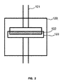
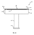
上述の高温処理とは対照的に、本発明の実施形態に従って製造することができる接合セラミック最終製品等の製品の例は、半導体処理に使用される加熱器アセンブリ又は他のタイプの基板支持台座の修理である。図1は、半導体処理に使用される加熱器等の基板支持台座100の形態にある例示的半導体処理部品を示している。一部の態様では、基板支持台座100は、窒化アルミニウム等のセラミックで構成される。加熱器は、プレート102を支持するシャフト101を有する。プレート102は、外側面103と呼ぶ場合もある上部面103を含む。シャフト101は、中空円筒とすることができる。プレート102は、平坦なディスクとすることができる。他の部分構成要素が存在することができる。この図ではプレート直径と比較して狭いシャフトを用いて示すが、本明細書で説明する修理処理は、広いベースを有する基板支持台座に適用することができる。
In contrast to the high temperature treatment described above, examples of products such as bonded ceramic final products that can be manufactured according to embodiments of the present invention are of heater assemblies or other types of substrate support pedestals used in semiconductor processing. It is a repair. FIG. 1 shows an exemplary semiconductor processing component in the form of a
図2は、プレス121を有する処理オーブン120を概念的に例示している。プレート122は、プレス121によって押圧されるように適応化された固定具123内に熱圧縮することができる。シャフト101は、処理段階で同様に製造することができる。典型的な処理では、プレート及びシャフトは、イットリア等の焼結助剤を約4重量%含有する窒化アルミニウムのモールド内への充填、それに続く一般的に「グリーン」セラミックと呼ばれる「固体」状態への窒化アルミニウム粉末の圧縮、更に続く窒化アルミニウム粉末を固体セラミック本体に緻密化する高温液相焼結処理によって形成される。高温液相焼結処理では、1700℃の範囲の温度及び2500psiの範囲の接触圧力がもたらされる場合がある。次いで、セラミック本体は、ダイヤモンド研磨を使用する標準の研削技術によって必要な形状に成形される。
FIG. 2 conceptually illustrates a
シャフトの機能は複数あり、1つは、加熱器要素、並びに加熱器プレート内に埋め込むことができる様々な他のタイプの電極に電力を印加するために真空チャンバの壁を通じた真空気密電気連通を与えることである。別のものは、熱電対等のモニタデバイスを用いた加熱器プレートの温度モニタを可能にし、この熱電対の材料と処理薬品との腐食等の相互作用を回避するためにこの熱電対が処理チャンバの外側に存在することを可能にすること、並びに熱電対接合部が高速反応に向けて非真空環境内で作動することを可能にすることである。別の機能は、上述の処理環境からの電気連通に使用される材料の絶縁を与えることである。電気連通に使用される材料は、一般的に金属性のものであり、従って、処理結果に対して有害であり、電気連通に使用される金属性材料の寿命に対して有害である可能性がある方法で処理環境に使用される処理薬品と相互作用する場合がある。 The shaft has multiple functions, one is vacuum airtight electrical communication through the walls of the vacuum chamber to apply power to the heater elements, as well as various other types of electrodes that can be embedded within the heater plate. Is to give. Another allows the temperature monitoring of the heater plate using a monitoring device such as a thermocouple, and this thermocouple is used in the processing chamber to avoid corrosion and other interactions between the material of the thermocouple and the processing chemicals. To allow it to be on the outside, as well as to allow the thermocouple junction to operate in a non-vacuum environment for fast reactions. Another function is to provide insulation for the materials used for electrical communication from the processing environment described above. The materials used for electrical communication are generally metallic and therefore may be detrimental to the treatment results and may be detrimental to the life of the metallic material used for electrical communication. It may interact with the treatment chemicals used in the treatment environment in some way.
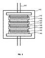
プレートの比較的平坦な性質を考えると、図3に概念的に見られるように、処理オーブン140内に存在するプレス141の軸線方向に沿って複数のプレートモールド成形固定具143を積み重ねることによって複数のプレート142を1回の処理において形成することができる。シャフトも、処理オーブン内でプレスを使用することで類似の処理において形成することができる。
Given the relatively flat nature of the plates, as conceptually seen in FIG. 3, a plurality of
半導体処理に使用される加熱器台座を製造する全体の処理において、プレートを形成する段階とシャフトを形成する段階の両方が、時間及びエネルギのかなりの投入を必要とする。物理的処理を有する特殊な高温オーブンのコストと、プレートを形成する処理段階及びシャフトを形成する処理段階が、各々数日にわたる特殊な処理オーブンの使用を必要とする可能性があることとを考えると、単にシャフト及びプレートが完成する点に至るまでの全処理を達成するだけで時間と資金の両方のかなりの投資が注ぎ込まれてしまっていることになる。現在の処理では、プレートをシャフトに固定するために特殊処理オーブンにおける更に別の段階が依然として必要とされる。この段階の例は、プレスを有する特殊高温処理オーブンにおける液相焼結段階を用いてシャフトをプレートに接合することであると考えられる。特殊処理オーブンにおけるこの第3の段階は、組み立て上がった加熱器構成がシャフトの長さとプレートの直径の両方を含むので、そのような処理オーブン内でかなりの空間を更に必要とする。シャフトのみの製造は類似の軸線方向長さ量を要する可能性があるが、シャフトの直径は、1回の処理において複数のシャフトを並列に製造することができるようなものである。 In the entire process of manufacturing the heater pedestal used for semiconductor processing, both the plate forming step and the shaft forming step require a considerable input of time and energy. Consider the cost of a special high temperature oven with physical treatment and the processing steps of forming the plate and forming the shaft may each require the use of a special processing oven for several days. And, simply achieving the entire process up to the point where the shaft and plate are completed would have invested a considerable amount of time and money. The current process still requires yet another step in the special process oven to secure the plate to the shaft. An example of this step would be to join the shaft to the plate using a liquid phase sintering step in a special high temperature processing oven with a press. This third step in a special processing oven requires considerable space in such a processing oven as the assembled heater configuration includes both the length of the shaft and the diameter of the plate. Manufacture of the shaft alone may require a similar amount of axial length, but the diameter of the shaft is such that multiple shafts can be manufactured in parallel in a single process.
図4で見られるように、シャフトをプレートに焼結する接合処理は、ここでもまた、プレス161を有する処理オーブン160の使用を必要とする。プレート162及びシャフト163を位置決めし、プレス161によって達成される圧力を伝達するために、固定具164、165のセットが使用される。
As seen in FIG. 4, the joining process of sintering the shaft to the plate also requires the use of a processing oven 160 with a press 161. A set of
加熱器台座が完成した状態で、それを半導体処理に対して使用することができる。加熱器台座は、腐食性ガス、高温、熱循環、及びガスプラズマを含む苛酷な条件下に使用される可能性が高い。更に、加熱器台座は、不用意な衝撃を受ける場合がある。プレート又はシャフトが損傷状態になった場合に、これらのデバイスを修理するための機会は限られていた。 Once the heater pedestal is complete, it can be used for semiconductor processing. The heater pedestal is likely to be used under harsh conditions including corrosive gases, high temperatures, heat circulation, and gas plasma. Further, the heater pedestal may be inadvertently impacted. Opportunities to repair these devices were limited if the plate or shaft became damaged.
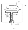
図5は、半導体処理チャンバに使用される加熱器台座円柱の一実施形態を示している。セラミック加熱器台座とすることができる加熱器台座300は、無線周波アンテナ310と、加熱器要素320と、シャフト330と、プレート340と、装着フランジ350とを含むことができる。無線周波アンテナ310は、装着プレートの上部面に非常に近い場合がある。
FIG. 5 shows an embodiment of a heater pedestal cylinder used in a semiconductor processing chamber. The
図6で見られるように、基板支持台座は、両方共に従来のろう付け材料に対して重大な問題を呈する可能性がある2つの明確に異なる雰囲気の間の空間を架橋する場合がある。加熱器205等の半導体処理機器の外側面207上では、材料は、加熱器205が内部に使用されることになる半導体処理チャンバ200内で発生する処理及びこのチャンバに存在する環境201に適合しなければならない。これらは、フッ素化学作用、及び極度に揮発性又は腐食性の化学作用を含む場合がある。加熱器205は、シャフト204によって支持されたプレート203の上部面に固定された基板206を有する場合がある。加熱器205の内面208上では、材料は、酸素化された雰囲気である場合がある異なる雰囲気202に適合しなければならない。銅、銀、又は金を含有する材料は、処理中のシリコンウェーハの格子構造と干渉する場合があり、従って、適切ではない。修理処理の一部としてろう付けを使用する可能性があるあらゆる修理に関して、ろう付け材料は、中空シャフトの中心部内の酸素化された雰囲気に露出される場合がある。この雰囲気に露出されることになるろう付け接合部の部分は酸化することになり、更に接合部内に酸化が進行する場合があり、接合部の密封不良がもたらされる。構造的な取り付けに加えて、半導体製造に使用されることになるこれらのデバイスのシャフト及びプレートの区域に使用されるろう付け材料は、殆ど又は全部ではないにしても多くの使用において密封性を有するべきである。
As seen in FIG. 6, both substrate support pedestals may bridge the space between two distinctly different atmospheres, both of which can pose significant problems to conventional brazing materials. On the
例示的実施形態では、プレートとシャフトは、両方共に窒化アルミニウムのものである場合がある。プレートは、一部の実施形態では直径が約9〜13インチ、厚みが0.5インチから0.75インチとすることができる。シャフトは、長さが5〜10インチで0.1インチの壁厚を有する中空円筒とすることができる。 In an exemplary embodiment, the plate and shaft may both be of aluminum nitride. The plate can be about 9 to 13 inches in diameter and 0.5 to 0.75 inches in thickness in some embodiments. The shaft can be a hollow cylinder with a length of 5-10 inches and a wall thickness of 0.1 inches.
本発明の一部の実施形態では、図7に記載の拡大図で見られるように、プレートアセンブリ201とシャフト202とを有するプレート及びシャフトデバイス200が見られる。プレートアセンブリ201は、層203、204、205を有する。最上位プレート層203は中間層204の上に重なり、最上位プレート層203と中間層204の間には電極層206が存在する。中間層204は最下位層205の上に重なり、中間層204と最下位層205の間には加熱器層207が存在する。
In some embodiments of the present invention, as seen in the enlarged view of FIG. 7, a plate and
プレートアセンブリ201の層203、204、205は、加熱器の場合は窒化アルミニウム等のセラミック、又は静電チャックの場合はAlN、ドープされたAlN、ベリリア、ドープされたベリリア、及びその他を含む他の材料のものである場合がある。プレートアセンブリの層203、204、205は、図7では別個のものであることを見ることができるが、実際にはこれらの層を全て固体セラミック部品の一部とすることができ、この場合に、シャフト、プレート層、加熱器、及び電極を含む構成要素の全てが、セラミックのホットプレス中に互いに組み立てられたものである。この場合に、基板支持台座はセラミック上部面を有することになり、加熱器、RFアンテナ、又はクランプ電極のいずれかがこの上部面の下にある。基板支持台座は、次の下側部分(加熱器のような)の上方の上部面の厚みが設計の重要な態様であるように設計されたものとすることができる。
基板支持台座の上部面が損傷状態になった時には、台座は、上部面が修理されない限り更に利用することができない。一部の態様では、上部面は、故障を低減又は除去するために上部面を研削することによって修理することができる。この手法に対する制限は、既に上部面が時には0.006インチ程度の薄さの非常に薄いものである場合があり、傷を除去するために十分に研削することを可能にするには十分な材料がない可能性があるということである。この手法に対する別の制限は、上部面が研削される時に、上部面の全厚が元の上部面層の厚みよりも小さく、それによって基板支持台座の最適以下のパフォーマンスがもたらされる場合があることである。 When the upper surface of the board support pedestal becomes damaged, the pedestal cannot be further utilized unless the upper surface is repaired. In some embodiments, the top surface can be repaired by grinding the top surface to reduce or eliminate failures. The limitation on this technique is that the top surface is already very thin, sometimes as thin as 0.006 inches, enough material to allow sufficient grinding to remove scratches. It is possible that there is no such thing. Another limitation of this technique is that when the top surface is ground, the total thickness of the top surface may be less than the thickness of the original top surface layer, which may result in suboptimal performance of the substrate support pedestal. Is.
本発明の一部の実施形態では、半導体処理部品、例えば、基板支持台座の上部の損傷材料は、ダイヤモンドビットを有する回転テーブルを使用するもの等の方法を用いて研削される。台座上部面は、最上位セラミック層の一部を貫通して研削することができ、又はセラミック内に埋め込まれた特徴部内に研削を更に進めることができる。一部の実施形態では、研削は、RFアンテナを除去することができる。新しい部品は、次に、基板支持台座の本明細書では場合によって機械加工面とも呼ぶ研削面に新しい部品、例えば、新しい上部シートを取り付けることになる材料を用い、かつ上記で解説したような台座が露出される可能性がある環境による悪影響を受けることにならないろう付け材料を用いて気密密封でろう付けすることによって取り付けることができる。一部の実施形態では、ろう付け層は、単純に台座の新しい上部面シートを取り付けるのに使用される。一部の実施形態では、ろう付け層はRFアンテナに置き換わり、RFアンテナとして機能する。取り扱い損傷及び設置中の損傷を抑制するために、初期状態において、新しい上部シートは、最終製品において望ましいものよりも厚い場合がある。次いで、元の台座に等しい寸法又は埋め込み加熱器の上方の上部面の深さ等の重要なパラメータに関して等しい寸法を完成した台座に与えるために、最上位層を研削することができる。 In some embodiments of the invention, the semiconductor processed component, eg, the damaging material on the top of the substrate support pedestal, is ground using methods such as those using a rotary table with diamond bits. The upper surface of the pedestal can be ground through a part of the uppermost ceramic layer, or the grinding can be further advanced in the feature portion embedded in the ceramic. In some embodiments, grinding can remove the RF antenna. The new part then uses a new part, eg, a material that will attach a new top sheet to the ground surface, sometimes referred to herein as the machined surface of the substrate support pedestal, and the pedestal as described above. Can be attached by brazing in an airtight seal with a brazing material that will not be adversely affected by the environment in which it may be exposed. In some embodiments, the brazing layer is simply used to attach a new top sheet of the pedestal. In some embodiments, the brazing layer replaces the RF antenna and functions as an RF antenna. In the initial state, the new topsheet may be thicker than desired in the final product to prevent handling damage and damage during installation. The top layer can then be ground to give the finished pedestal dimensions equal to the original pedestal or with respect to important parameters such as the depth of the upper surface above the embedded heater.
一部の態様では、新しいセラミック最上位層又は他の新しい部品を半導体処理部品に取り付けるろう付け層が密封接合部をもたらすことが重要である場合がある。元の台座の上部面が研削される時に、台座が後に半導体の製造において内部に使用されることになるチャンバの内側の環境に耐えることができない態様がこの面にもたらされる場合がある。更に、あらゆる実質的な漏れを排除するために良好で完全な湿潤及び密封性が望ましく、この場合に、非密封ろう付け層により、ろう付け内の空隙内に閉じ込められたガスが、台座が後に内部に使用されるチャンバ内に「漏れて」入る。この漏れは望ましい状態ではない。更に、空隙がなく完全に湿潤した密封接合部は、埋め込み加熱器と台座の上部面の間により均等な熱伝導率を有するより不変で均等な熱経路を与えることになる。 In some embodiments, it may be important that the brazed layer that attaches the new ceramic top layer or other new component to the semiconductor processed component provides a sealed joint. When the upper surface of the original pedestal is ground, this surface may be incapable of withstanding the environment inside the chamber, which will later be used internally in the manufacture of semiconductors. In addition, good and complete wetting and sealing is desirable to eliminate any substantial leakage, in which case the unsealed brazing layer allows the gas trapped in the voids within the brazing to be pedestaled later. "Leaks" into the chamber used inside. This leak is not a desirable condition. In addition, a completely moist sealed joint with no voids will provide a more invariant and uniform heat path with more uniform thermal conductivity between the embedded heater and the upper surface of the pedestal.
例示的実施形態では、外側面にある程度の損傷を有する基板支持台座の形態にある半導体処理部品が修理に向けて与えられる。上部面又は外側面を含む損傷部分は、例えば、セラミックを貫通して研削される。一実施形態では、この部分は、RFアンテナに至るまで研削される。一部の実施形態では、RFアンテナの深さは十分な精度で既知であり、従って、機械加工を既知の切断深さに達するように設定することができる。RFアンテナが露出された状態で、機械加工をRFアンテナが除去されるまで続行することができる。RFアンテナの下から来るリードに予め取り付けられたものとすることができるRFアンテナのリードパッドを見ることができ、リードの場所が示される。RFアンテナに結合されていた同じリードは、置換RFアンテナへのリードとして留まることになる。例えば、アルミニウムから構成され、下記で解説するろう付け層を機械加工された台座のその上に配置又は堆積させることができる。次いで、新しい部品、例えば、一部の態様ではAlNとすることができる新しいセラミック最上位層が、プレアセンブリの上に配置される。次いで、プレアセンブリを真空チャンバとすることができる処理オーブンに配置することができる。その後に、アセンブリが互いにろう付けされる。ろう付け後に、台座の元の高さとすることができる望ましい高さを台座に与えるために、新しいセラミック最上位層を機械加工することができる。 In an exemplary embodiment, a semiconductor-treated component in the form of a substrate support pedestal with some damage to the outer surface is provided for repair. The damaged portion, including the top or outer surface, is ground, for example, through the ceramic. In one embodiment, this portion is ground down to the RF antenna. In some embodiments, the depth of the RF antenna is known with sufficient accuracy, so machining can be set to reach a known cutting depth. With the RF antenna exposed, machining can continue until the RF antenna is removed. You can see the reed pad of the RF antenna, which can be pre-attached to the reed coming from under the RF antenna, and the location of the reed is indicated. The same lead coupled to the RF antenna will remain as a lead to the replacement RF antenna. For example, a brazing layer made of aluminum and described below can be placed or deposited on a machined pedestal. A new part, eg, a new ceramic top layer, which in some embodiments can be AlN, is placed on top of the preassembly. The preassembly can then be placed in a processing oven that can be a vacuum chamber. The assemblies are then brazed to each other. After brazing, a new ceramic top layer can be machined to give the pedestal a desired height that can be the original height of the pedestal.
例示的実施形態では、台座の最上位層は、新しいセラミック最上位層と同じく窒化アルミニウムである。ろう付け層は99.9%アルミニウムであり、台座上に堆積させたものであり、30ミクロン厚である。一部の実施形態では、ろう付け層はアルミニウムホイルとすることができ、ろう付けの前には15〜200ミクロン厚とすることができる。新しいセラミック最上位層は、設置及びろう付け中には0.125インチとすることができ、その後に0.040インチまで機械研削することができる。ろう付けは、850℃で10分間行われる。ろう付けは、1×10E−4トルよりも低い圧力で行われる。 In an exemplary embodiment, the top layer of the pedestal is aluminum nitride, as is the new ceramic top layer. The brazing layer is 99.9% aluminum, deposited on a pedestal and is 30 microns thick. In some embodiments, the brazing layer can be aluminum foil and can be 15-200 microns thick prior to brazing. The new ceramic top layer can be 0.125 inches during installation and brazing and then mechanically ground to 0.040 inches. Brazing is performed at 850 ° C. for 10 minutes. Brazing is performed at a pressure lower than 1 x 10E-4 torr.
一部の実施形態では、新しいセラミック最上位層は、800℃で2分から10分までにわたって台座にろう付けすることができる。一部の実施形態では、新しいセラミック最上位層は、800℃で10分から100分までにわたって台座にろう付けすることができる。一部の実施形態では、新しいセラミック最上位層は、1200℃で2分から100分までにわたって台座にろう付けすることができる。一部の実施形態では、新しいセラミック最上位層は、770℃で2分から10分までにわたって台座にろう付けすることができる。一部の実施形態では、新しいセラミック最上位層は、770℃で10分から100分までにわたって台座にろう付けすることができる。一部の実施形態では、新しいセラミック最上位層は、1200℃で2分から100分までにわたって台座にろう付けすることができる。最も近い50℃区分に対して丸めると、必要とされる最低温度は800℃とすることができる。最も近い10℃区分に対して丸めると、必要とされる最低温度は770℃とすることができる。 In some embodiments, the new ceramic top layer can be brazed to the pedestal at 800 ° C. for 2 to 10 minutes. In some embodiments, the new ceramic top layer can be brazed to the pedestal at 800 ° C. for 10 to 100 minutes. In some embodiments, the new ceramic top layer can be brazed to the pedestal at 1200 ° C. for 2 to 100 minutes. In some embodiments, the new ceramic top layer can be brazed to the pedestal at 770 ° C. for 2 to 10 minutes. In some embodiments, the new ceramic top layer can be brazed to the pedestal at 770 ° C. for 10 to 100 minutes. In some embodiments, the new ceramic top layer can be brazed to the pedestal at 1200 ° C. for 2 to 100 minutes. Rounded to the nearest 50 ° C. division, the minimum required temperature can be 800 ° C. Rounded to the nearest 10 ° C. division, the minimum required temperature can be 770 ° C.
本発明の一部の実施形態では、基板支持台座又は他の半導体処理部品の上部の上の損傷材料は、ダイヤモンドビットを有する回転テーブルを使用するもの等の方法を用いて研削される。台座上部面は、最上位セラミック層の一部を貫通して研削することができ、又はセラミック内に埋め込された特徴部内に研削を更に進めることができる。一部の実施形態では、研削は、クランプ電極を除去することができる。次いで、上部シートを基板支持台座の研削面にこの上部シートを取り付けることになる材料を用い、かつ上記で解説したような台座が露出される可能性がある環境による悪影響を受けることにならないろう付け材料を用いて気密密封でろう付けすることによって取り付けることができる。一部の実施形態では、ろう付け層はクランプ電極に置き換わり、クランプ電極として機能する。取り扱い損傷及び設置中の損傷を抑制するために、初期状態において、新しい上部シートは、最終製品において望ましいものよりも厚い場合がある。次いで、元の台座に等しい寸法又は埋め込み加熱器の上方の上部面の深さ等の重要なパラメータに関して等しい寸法を完成した台座に与えるために、又は基板の静電グリップを容易するために最上位層を研削することができる。 In some embodiments of the invention, the damaging material on the substrate support pedestal or the top of other semiconductor processed components is ground using methods such as those using a rotary table with diamond bits. The upper surface of the pedestal can be ground through a part of the uppermost ceramic layer, or the grinding can be further advanced in the feature portion embedded in the ceramic. In some embodiments, grinding can remove the clamp electrodes. The upper sheet is then brazed using the material that would attach the upper sheet to the ground surface of the substrate support pedestal and without being adversely affected by the environment where the pedestal may be exposed as described above. It can be attached by brazing with a material that is airtightly sealed. In some embodiments, the brazing layer replaces the clamp electrode and functions as a clamp electrode. In the initial state, the new topsheet may be thicker than desired in the final product to prevent handling damage and damage during installation. Top-level to provide the finished pedestal with dimensions equal to the original pedestal or with respect to important parameters such as the depth of the upper top surface of the embedded heater, or to facilitate electrostatic grip on the substrate. The layer can be ground.
一部の態様では、新しいセラミック最上位層又は他の部品を台座に取り付けるろう付け層が密封接合部をもたらすことが重要である場合がある。元の台座の上部面が研削される時に、台座が後に半導体の製造において内部に使用されることになるチャンバの内側の環境に耐えることができない態様がこの面にもたらされる場合がある。更に、あらゆる実質的な漏れを排除するために良好で完全な湿潤及び密封性が望ましく、この場合に、非密封ろう付け層により、ろう付け内の空隙内に閉じ込められたガスが、台座が後に内部に使用されるチャンバ内に「漏れて」入る。この漏れは望ましい状態ではない。更に、空隙がなく完全に湿潤した密封接合部は、埋め込み加熱器と台座の上部面の間により均等な熱伝導率を有するより不変で均等な熱経路を与えることになる。 In some embodiments, it may be important that a new ceramic top layer or brazing layer that attaches other components to the pedestal provides a sealed joint. When the upper surface of the original pedestal is ground, this surface may be incapable of withstanding the environment inside the chamber, which will later be used internally in the manufacture of semiconductors. In addition, good and complete wetting and sealing is desirable to eliminate any substantial leakage, in which case the unsealed brazing layer allows the gas trapped in the voids within the brazing to be pedestaled later. "Leaks" into the chamber used inside. This leak is not a desirable condition. In addition, a completely moist sealed joint with no voids will provide a more invariant and uniform heat path with more uniform thermal conductivity between the embedded heater and the upper surface of the pedestal.
例示的実施形態では、上部面にある程度の損傷を有する基板支持台座が修理に向けて与えられる。一実施形態では、上部面は、セラミックを貫通してクランプ電極に至るまで研削される。一部の実施形態では、クランプ電極の深さは十分な精度で既知であり、従って、機械加工を既知の切断深さに達するように設定することができる。クランプ電極が露出された状態で、機械加工をクランプ電極が除去されるまで続行することができる。クランプ電極の下から来るリードに予め取り付けられたものとすることができるクランプ電極のリードパッドを見ることができ、リードの場所が示される。クランプ電極に結合されていた同じリードは、置換クランプ電極へのリードとして留まることになる。例えば、アルミニウムから構成され、下記で解説するろう付け層は、機械加工された台座のその上に配置又は堆積させることができる。次いで、一部の態様ではAlNとすることができる新しいセラミック最上位層が、プレアセンブリの上に配置される。次いで、プレアセンブリを真空チャンバとすることができる処理オーブンに配置することができる。その後に、アセンブリが互いにろう付けされる。ろう付け後に、台座の元の高さとすることができる望ましい高さを台座に与えるために、新しいセラミック最上位層を機械加工することができる。 In an exemplary embodiment, a substrate support pedestal with some damage to the top surface is provided for repair. In one embodiment, the top surface is ground through the ceramic to the clamp electrodes. In some embodiments, the depth of the clamp electrode is known with sufficient accuracy, so machining can be set to reach a known cutting depth. With the clamp electrodes exposed, machining can continue until the clamp electrodes are removed. The lead pad of the clamp electrode, which can be pre-attached to the lead coming from under the clamp electrode, can be seen and the location of the lead is indicated. The same leads attached to the clamp electrode will remain as leads to the replacement clamp electrode. For example, a brazing layer made of aluminum and described below can be placed or deposited on top of a machined pedestal. A new ceramic top layer, which in some embodiments can be AlN, is then placed on top of the preassembly. The preassembly can then be placed in a processing oven that can be a vacuum chamber. The assemblies are then brazed to each other. After brazing, a new ceramic top layer can be machined to give the pedestal a desired height that can be the original height of the pedestal.
例示的実施形態では、台座の最上位層は、新しいセラミック最上位層と同じく窒化アルミニウムである。ろう付け層は99.9%アルミニウムであり、台座上に堆積させたものであり、30ミクロン厚である。一部の実施形態では、ろう付け層はアルミニウムホイルとすることができ、ろう付けの前には15〜200ミクロン厚とすることができる。新しいセラミック最上位層は、設置及びろう付け中には0.125インチとすることができ、その後に例えば0.008インチから0.040インチまで機械研削することができる。ろう付けは、850℃で10分間行われる。ろう付けは、1×10E−4トルよりも低い圧力で行われる。 In an exemplary embodiment, the top layer of the pedestal is aluminum nitride, as is the new ceramic top layer. The brazing layer is 99.9% aluminum, deposited on a pedestal and is 30 microns thick. In some embodiments, the brazing layer can be aluminum foil and can be 15-200 microns thick prior to brazing. The new ceramic top layer can be 0.125 inches during installation and brazing, followed by mechanical grinding from, for example, 0.008 inches to 0.040 inches. Brazing is performed at 850 ° C. for 10 minutes. Brazing is performed at a pressure lower than 1 x 10E-4 torr.
一部の実施形態では、新しいセラミック最上位層は、800℃で2分から10分までにわたって台座にろう付けすることができる。一部の実施形態では、新しいセラミック最上位層は、800℃で10分から100分までにわたって台座にろう付けすることができる。一部の実施形態では、新しいセラミック最上位層は、1200℃で2分から100分までにわたって台座にろう付けすることができる。一部の実施形態では、新しいセラミック最上位層は、770℃で2分から10分までにわたって台座にろう付けすることができる。一部の実施形態では、新しいセラミック最上位層は、770℃で10分から100分までにわたって台座にろう付けすることができる。一部の実施形態では、新しいセラミック最上位層は、1200℃で2分から100分までにわたって台座にろう付けすることができる。最も近い50℃区分に対して丸めると、必要とされる最低温度は800℃とすることができる。最も近い10℃区分に対して丸めると、必要とされる最低温度は770℃とすることができる。 In some embodiments, the new ceramic top layer can be brazed to the pedestal at 800 ° C. for 2 to 10 minutes. In some embodiments, the new ceramic top layer can be brazed to the pedestal at 800 ° C. for 10 to 100 minutes. In some embodiments, the new ceramic top layer can be brazed to the pedestal at 1200 ° C. for 2 to 100 minutes. In some embodiments, the new ceramic top layer can be brazed to the pedestal at 770 ° C. for 2 to 10 minutes. In some embodiments, the new ceramic top layer can be brazed to the pedestal at 770 ° C. for 10 to 100 minutes. In some embodiments, the new ceramic top layer can be brazed to the pedestal at 1200 ° C. for 2 to 100 minutes. Rounded to the nearest 50 ° C. division, the minimum required temperature can be 800 ° C. Rounded to the nearest 10 ° C. division, the minimum required temperature can be 770 ° C.
本発明の一部の実施形態では、基板支持台座の上部の上の損傷材料は、ダイヤモンドビットを有する回転テーブルを使用するもの等の方法を用いて研削される。台座上部面は、最上位セラミック層の一部を貫通して研削することができ、又はセラミック内に埋め込まれた特徴部内に研削を更に進めることができる。一部の実施形態では、研削は、加熱器の上方のセラミックのみを除去することができる。次いで、上部シートを基板支持台座の研削面にこの上部シートを取り付けることになる材料を用い、かつ上記で解説したような台座が露出される可能性がある環境による悪影響を受けることにならないろう付け材料を用いて気密密封でろう付けすることによって取り付けることができる。一部の実施形態では、ろう付け層は、単に台座の新しい上部面シートを取り付けるのに使用される。取り扱い損傷及び設置中の損傷を抑制するために、初期状態において、新しい上部シートは、最終製品において望ましいものよりも厚い場合がある。次いで、元の台座に等しい寸法又は埋め込み加熱器の上方の上部面の深さ等の重要なパラメータに関して等しい寸法を完成した台座に与えるために、又は基板の静電グリップを容易するために最上位層を研削することができる。 In some embodiments of the invention, the damaging material above the top of the substrate support pedestal is ground using methods such as those using a rotary table with diamond bits. The upper surface of the pedestal can be ground through a part of the uppermost ceramic layer, or the grinding can be further advanced in the feature portion embedded in the ceramic. In some embodiments, grinding can only remove the ceramic above the heater. The upper sheet is then brazed using the material that would attach the upper sheet to the ground surface of the substrate support pedestal and without being adversely affected by the environment where the pedestal may be exposed as described above. It can be attached by brazing with a material that is airtightly sealed. In some embodiments, the brazing layer is simply used to attach a new top sheet of the pedestal. In the initial state, the new topsheet may be thicker than desired in the final product to prevent handling damage and damage during installation. Top-level to provide the finished pedestal with dimensions equal to the original pedestal or with respect to important parameters such as the depth of the upper top surface of the embedded heater, or to facilitate electrostatic grip on the substrate. The layer can be ground.
一部の態様では、新しいセラミック最上位層を台座に取り付けるろう付け層が密封接合部をもたらすことが重要である場合がある。元の台座の上部面が研削される時に、台座が後に半導体の製造において内部に使用されることになるチャンバの内側の環境に耐えることができない態様がこの面にもたらされる場合がある。更に、あらゆる実質的な漏れを排除するために良好で完全な湿潤及び密封性が望ましく、この場合に、非密封ろう付け層により、ろう付け内の空隙内に閉じ込められたガスが、台座が後に内部に使用されるチャンバ内に「漏れて」入る。この漏れは望ましい状態ではない。更に、空隙がなく完全に湿潤した密封接合部は、埋め込み加熱器と台座の上部面の間により均等な熱伝導率を有するより不変で均等な熱経路与えることになる。 In some embodiments, it may be important that the brazing layer that attaches the new ceramic top layer to the pedestal provides a sealed joint. When the upper surface of the original pedestal is ground, this surface may be incapable of withstanding the environment inside the chamber, which will later be used internally in the manufacture of semiconductors. In addition, good and complete wetting and sealing is desirable to eliminate any substantial leakage, in which case the unsealed brazing layer allows the gas trapped in the voids within the brazing to be pedestaled later. "Leaks" into the chamber used inside. This leak is not a desirable condition. In addition, a completely moist sealed joint with no voids will provide a more invariant and uniform heat path with more uniform thermal conductivity between the embedded heater and the upper surface of the pedestal.
例示的実施形態では、上部面にある程度の損傷を有する基板支持台座が修理に向けて与えられる。上部面は、セラミックを貫通して加熱器の上方のある距離まで研削される。加熱器を損傷しないように、加熱器の上方のターゲット残存セラミックは、0.100インチとすることができる。例えば、アルミニウムから構成され、下記で解説するろう付け層は、機械加工された台座のその上に配置又は堆積させることができる。次いで、一部の態様ではAlNとすることができる新しいセラミック最上位層が、プレアセンブリの上に配置される。次いで、プレアセンブリを真空チャンバとすることができる処理オーブンに配置することができる。その後に、アセンブリが互いにろう付けされる。ろう付け後に、台座の元の高さとすることができる望ましい高さを台座に与えるために、新しいセラミック最上位層を機械加工することができる。 In an exemplary embodiment, a substrate support pedestal with some damage to the top surface is provided for repair. The top surface is ground through the ceramic to a distance above the heater. The target residual ceramic above the heater can be 0.100 inches so as not to damage the heater. For example, a brazing layer made of aluminum and described below can be placed or deposited on top of a machined pedestal. A new ceramic top layer, which in some embodiments can be AlN, is then placed on top of the preassembly. The preassembly can then be placed in a processing oven that can be a vacuum chamber. The assemblies are then brazed to each other. After brazing, a new ceramic top layer can be machined to give the pedestal a desired height that can be the original height of the pedestal.
例示的実施形態では、台座の最上位層は、新しいセラミック最上位層と同じく窒化アルミニウムである。ろう付け層は、99.9%アルミニウムであり、台座上に堆積させたものであり、かつ30ミクロン厚である。一部の実施形態では、ろう付け層はアルミニウムホイルとすることができ、ろう付けの前には15〜200ミクロン厚とすることができる。新しいセラミック最上位層は、設置及びろう付け中には0.125インチとすることができ、その後に例えば0.040インチから0.060インチまで機械研削することができる。ろう付けは、850℃で10分間行われる。ろう付けは、1×10E−4トルよりも低い圧力で行われる。 In an exemplary embodiment, the top layer of the pedestal is aluminum nitride, as is the new ceramic top layer. The brazing layer is 99.9% aluminum, deposited on a pedestal, and is 30 microns thick. In some embodiments, the brazing layer can be aluminum foil and can be 15-200 microns thick prior to brazing. The new ceramic top layer can be 0.125 inches during installation and brazing, followed by mechanical grinding from, for example, 0.040 inches to 0.060 inches. Brazing is performed at 850 ° C. for 10 minutes. Brazing is performed at a pressure lower than 1 x 10E-4 torr.
一部の実施形態では、新しいセラミック最上位層は、800℃で2分から10分までにわたって台座にろう付けすることができる。一部の実施形態では、新しいセラミック最上位層は、800℃で10分から100分までにわたって台座にろう付けすることができる。一部の実施形態では、新しいセラミック最上位層は、1200℃で2分から100分までにわたって台座にろう付けすることができる。 In some embodiments, the new ceramic top layer can be brazed to the pedestal at 800 ° C. for 2 to 10 minutes. In some embodiments, the new ceramic top layer can be brazed to the pedestal at 800 ° C. for 10 to 100 minutes. In some embodiments, the new ceramic top layer can be brazed to the pedestal at 1200 ° C. for 2 to 100 minutes.
図8は、本発明の一部の実施形態による台座上プレート260の断面を示している。台座上プレート260は、異なる層の間に加熱器と電極の両方が存在する多層プレートアセンブリである。新しい最上位層は、ろう付け要素266と接合される。一部の実施形態では、プレートの平面に対して垂直な方向の新しい最上位プレート層の最終位置は、プレート上のスタンドオフ268によって決定される。 FIG. 8 shows a cross section of the pedestal plate 260 according to some embodiments of the present invention. The pedestal plate 260 is a multi-layer plate assembly in which both heaters and electrodes are present between different layers. The new top layer is joined with the brazing element 266. In some embodiments, the final position of the new top plate layer in the direction perpendicular to the plane of the plate is determined by standoffs 268 on the plate.
新しいセラミック最上位層261は、下側部分262の上に重なる。最上位プレート層261は、多機能接合層266を用いて下側部分262に接合される。多機能接合層266は、下側プレート部分262への新しいセラミック最上位層261の接合を与え、電極になるように適応化される。そのような電極は、実質的に円形のディスクである接合層とすることができ、接合材料も電極として機能する。図36で見られるように、スタンドオフ268は、下側プレート層262に対する最上位プレート層261のこれらのプレート層の主平面に対して垂直な鉛直方向の位置制御を与えるように適応化される。一部の実施形態では、ろう付け層は、位置制御が必要とされないか又は実施されない程薄いとすることができる。最上位プレート層261のリムは、2つのプレートの周りにおいてこれらのプレートの間の境界に沿う視線を取り除くように適応化される。接合層266の厚みは、プレートアセンブリを加熱及び接合する段階の前に接合層266が最上位プレート層261及び下側プレート層262と接触しているようにサイズ決定することができる。
The new ceramic
新しいセラミック最上位層を接合するためのプレートアセンブリの接合段階中に、図8に見られる構成要素を事前に組み立てることができ、次いで、完成した修理された基板支持台座を形成するために、本明細書で説明する処理を用いてこのプレートプレアセンブリを接合することができる。 During the joining phase of the plate assembly for joining the new ceramic top layers, the components seen in FIG. 8 can be preassembled and then the book to form the completed repaired substrate support pedestal. The plate preassembly can be joined using the process described herein.
本発明の一部の実施形態では、図15に見られるように、静電チャック300は、シャフト302に接合されたプレートアセンブリ301を有することができる。シャフト302は、中空とすることができ、装着フランジ303を有することができる。プレートアセンブリ301は、処理中にウェーハ又は他の基板を支持するように適応化された新しい上部面308を有する。新しい最上位層305は、ろう付け層306を用いて下側プレート部分304に接合することができる。最上位層305と下側プレート部分304の間にはクランプ電極307が存在することができる。チャンバからの電極の電気絶縁を与えるために、クランプ電極307は、ろう付け層306から間隙309によって分離することができる。
In some embodiments of the invention, as seen in FIG. 15, the
図16は、基板の取り外しのためのピンを有する静電チャックと併用することができるクランプ電極336の態様を示している。図16は、上側プレート層と中間プレート層の間で第1の密封リング334を通る鉛直断面図として見ることができる。クランプ電極336は、静電チャックによって支持された基板にクランプ力を与えるように適応化される。第1の密封リング334はプレート層330の円周周囲の周りに見られる。第1の密封リング334とクランプ電極336の間の間隙333は、間隙335を通して電気絶縁を与える。ピン孔331の各々は、その周囲の周りに密封リング332を有する。密封リング332は、それとクランプ電極336の間に間隙333を有する。
FIG. 16 shows an aspect of a
本発明の一部の実施形態による接合方法は、湿潤の制御と、接合されるセラミック部品に対する接合材料の流れとに頼る。一部の実施形態では、接合処理の間の酸素の欠如が、接合区域内の材料を変化させる反応を伴わない適正な湿潤を可能にする。適正な湿潤と接合材料の流れとを使用することで、例えば、液相焼結と比較して低い温度で密封接合部を達成することができる。 The bonding method according to some embodiments of the present invention relies on wettability control and the flow of bonding material to the ceramic component to be bonded. In some embodiments, the lack of oxygen during the joining process allows proper wetting without a reaction that changes the material within the joining area. By using proper wetting and flow of bonding material, a sealed junction can be achieved, for example, at a lower temperature compared to liquid phase sintering.
接合されたセラミックの最終製品が使用される一部の用途では、接合部の強度は、重要な設計ファクタではない場合がある。一部の用途では、接合部のいずれかの側の雰囲気の分離を可能にするために接合部の密封性を必要とする場合がある。一部の用途では、ろう付け層の実質的な漏れを防止するために接合部の密封性を必要とする場合がある。同じく、セラミックアセンブリ及び製品が露出される可能性がある化学物質に対して耐性を有するような接合材料の組成が重要である場合がある。接合材料は、これらの化学物質に対して耐性を有する必要がある場合があり、そうでなければ接合部の変性及び気密密封の消失をもたらす場合がある。同じく、接合材料は、完成したセラミックデバイスによって後にサポートされる処理と有害に干渉しないタイプの材料のものである必要がある可能性もある。 In some applications where the final product of the joined ceramic is used, the strength of the joint may not be an important design factor. Some applications may require joint sealing to allow separation of the atmosphere on either side of the joint. Some applications may require joint sealing to prevent substantial leakage of the brazing layer. Similarly, the composition of the bonding material may be important so that the ceramic assembly and the product are resistant to the chemicals that may be exposed. The joint material may need to be resistant to these chemicals, otherwise it may result in modification of the joint and loss of airtight seal. Similarly, the bonding material may need to be of a type that does not adversely interfere with the treatments that are later supported by the finished ceramic device.
図9は、本発明の一部の実施形態による接合部10の断面図である。この画像は走査電子顕微鏡(SEM)を通して見たものであり、20,000×の倍率で撮影されたものである。第1のセラミック部品11が、接合層13を用いて第2のセラミック部品12に接合されている。この例示的実施形態では、第1のセラミック部品及び第2のセラミック部品は、単結晶窒化アルミニウム(AlN)で製造されたものである。接合層は、0.4重量%のFeを有するアルミニウムホイルとして始まるものであった。接合温度は1200℃であり、120分間保持した。接合は、7.3×10E−5トルの真空下で接合中に接合部の両側で約290psiの物理的接触圧力を用いて行った。
FIG. 9 is a cross-sectional view of the joint portion 10 according to a part of the embodiment of the present invention. This image was viewed through a scanning electron microscope (SEM) and was taken at a magnification of 20,000 x. The first ceramic component 11 is bonded to the second
下記の解説は、密封接合部をもたらすろう付け処理の例を含む。図1は、第1のセラミック部品11と接合層13の間の上側境界15と、接合層13と第2のセラミック部品12の間の下側境界16とを有する接合部を示している。20,000×の倍率で境界領域において見られるように、セラミック部品内への接合層の拡散は見られない。セラミック内の反応の痕跡は見られない。境界は、いかなる空隙の痕跡も示しておらず、接合処理中にアルミニウムによる境界の完全な湿潤があったことを示している。接合層内に見られる明るいスポット14はアルミニウム−鉄化合物であり、鉄は、接合層に使用されたホイルからの残留物である。
The following description includes an example of a brazing process that results in a sealed joint. FIG. 1 shows a junction having an upper boundary 15 between the first ceramic component 11 and the
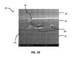
図10は、本発明の一部の実施形態による接合部20の断面図である。この図は走査電子顕微鏡(SEM)を通して見たものであり、80,000×の倍率におけるものである。第1のセラミック部品21が、接合層23を用いて第2のセラミック部品22に接合されている。この例示的実施形態では、第1のセラミック部品及び第2のセラミック部品は、単結晶窒化アルミニウム(AlN)で製造されたものである。接合層は、0.4重量%のFeを有するアルミニウムホイルとして始まるものであった。接合温度は900℃であり、15分間保持した。接合は、1.9×10E−5トルの真空下で接合中に接合部の両側で最小の物理的接触圧力を用いて行った。接合層23は、第1のセラミック部品21と第2の部品22との接合後に、接合された部品の間にアルミニウムの残存層が残ることを示している。
FIG. 10 is a cross-sectional view of the
図10は、第1のセラミック部品21と接合層23の間の上側境界24と、接合層23と第2のセラミック部品22の間の下側境界25とを有する接合部を示している。8,000×の倍率で境界領域において見られるように、セラミック部品内への接合層の拡散は見られない。セラミック内の反応の痕跡は見られない。境界は、いかなる空隙の痕跡も示しておらず、接合処理中にアルミニウムによる境界の完全な湿潤があったことを確実に示している。接合層内に見られる明るいスポット26は、接合層に使用されたホイルからのFe残留物を含む。
FIG. 10 shows a joint having an
図9及び図10は、単結晶窒化アルミニウム等のセラミックが、接合処理中に完全湿潤をもたらしたアルミニウムの接合層で接合される本発明の実施形態による接合部を示している。これらの接合部は、セラミック内への接合層の拡散の痕跡、及び接合層の内部又はセラミック部品内の反応の痕跡を示していない。セラミック部品又は接合層内における化学変換の痕跡はない。接合処理後のアルミニウムの残存層が存在する。 9 and 10 show a joint according to an embodiment of the present invention in which a ceramic such as single crystal aluminum nitride is joined by a joint layer of aluminum that has been completely moistened during the joining process. These junctions show no evidence of diffusion of the junction layer into the ceramic and no evidence of reaction inside the junction layer or within the ceramic component. There is no evidence of chemical conversion within the ceramic part or junction layer. There is a residual layer of aluminum after the joining process.
図11は、多結晶窒化アルミニウムセラミックを使用する本発明の実施形態による接合部30を示している。図3では、下側セラミック部品31に接合された接合層32が見られる。この図は走査電子顕微鏡(SEM)を通して見たものであり、4,000×の倍率におけるものである。この例示的実施形態では、第1のセラミック部品は多結晶窒化アルミニウム(AlN)で製造されたものである。接合層は、0.4重量%のFeを有するアルミニウムホイルとして始まるものであった。接合温度は1200℃であり、60分間保持した。接合は、2.4×10E−5トルの真空下で接合中に接合部の両側で約470psiの物理的接触圧力を用いて行った。
FIG. 11 shows a joint 30 according to an embodiment of the present invention using a polycrystalline aluminum nitride ceramic. In FIG. 3, the
一部の実施形態では、図11〜図13に見られるセラミック等の多結晶AlNは、96%のAlNと4%のイットリアとで構成される。そのようなセラミックは、それを製造するのに使用される液相焼結中に低温を使用することができることで産業用途に使用することができる。低温処理は、単結晶AlNとは対照的に、セラミックの製造エネルギ消費量及びコストを低減する。多結晶材料は、それ程脆弱ではないことのような好ましい特性を有することができる。イットリア及びSm2O3等の他のドーパントは、製造可能性及び材料特性の調整の理由から多くの場合に使用される。 In some embodiments, the polycrystalline AlNs such as ceramics found in FIGS. 11-13 are composed of 96% AlN and 4% yttria. Such ceramics can be used in industrial applications due to the ability to use low temperatures during the liquid phase sintering used to make them. Cold treatment reduces the energy consumption and cost of producing ceramics, as opposed to single crystal AlN. Polycrystalline materials can have favorable properties such as not being so brittle. Other dopants such as Itria and Sm2O3 are often used for reasons of manufacturability and adjustment of material properties.
図11は、図1及び図2に示す単結晶の例の場合に見られるように、接合層32と多結晶AlNセラミックである第1のセラミック部品31との間の境界33における拡散の欠如を示している。境界33は、図1及び図2に見られるものよりも幾分粗く見える場合があるが、これは粗めの元の面の結果である。境界に沿って拡散は見られない。
FIG. 11 shows the lack of diffusion at the boundary 33 between the
図11〜図13に見られる96%AlN−4%イットリア等の多結晶AlNの場合に、セラミックは、アルミン酸イットリウムが散在するAlNの粒子を呈する。このセラミックに本発明の一部の実施形態による接合層等のアルミニウムがAlの液相温度よりも大きいもの等の高温で与えられると、Alろう付け材料がアルミン酸イットリウムと反応することができ、セラミックの面においてAl粒子の一部の遊離及び放出がもたらされる。 In the case of polycrystalline AlN such as 96% AlN-4% yttria seen in FIGS. 11 to 13, the ceramic exhibits particles of AlN interspersed with yttrium aluminate. When aluminum such as a bonding layer according to a part of the present invention is applied to this ceramic at a high temperature such as one having a temperature higher than the liquid phase temperature of Al, the Al brazing material can react with ittrium aluminate. It results in the release and release of some of the Al particles on the surface of the ceramic.
図12は、多結晶窒化アルミニウムセラミックを使用する本発明の実施形態による接合部40を示している。図4では、上側セラミック部品42を下側セラミック部品41に接合する接合層43が見られる。この図は走査電子顕微鏡(SEM)を通して見たものであり、8,000×の倍率におけるものである。この例示的実施形態では、第1のセラミック部品は多結晶窒化アルミニウム(AlN)で製造されたものである。接合層は、99.8%のAlを有するアルミニウムホイルとして始まるものであった。接合温度は1120℃であり、60分間保持した。接合は、2.0×10E−5トルの真空下で接合中に接合部の両側で最小の物理的接触圧力を用いて行った。
FIG. 12 shows a joint 40 according to an embodiment of the present invention using a polycrystalline aluminum nitride ceramic. In FIG. 4, a
図12は、接合層43内に一部のAlN粒子46を示している。粒子46は、上側セラミック部品42の面44及び/又は下側セラミック部品41の面45から移動したものである。これらのAlN粒子は、接合層のアルミニウムが多結晶AlNの粒子の間のアルミン酸イットリウムを侵食したことに起因して面から遊離したものである。AlN粒子自体はアルミニウム接合層と反応しておらず、見られるAlN粒子内へのアルミニウムのいかなる拡散兆候もない。本発明の実施形態による処理条件下でのアルミニウムによる拡散に対するAlNの非感受性は、先に図1及び図2の単結晶AlNの例において見られており、図4の多結晶の例において維持されている。
FIG. 12 shows some
図13は、多結晶窒化アルミニウムセラミックを使用する本発明の実施形態による接合部50を示している。図5では、上側セラミック部品51に接合された接合層52が見られる。この図は走査電子顕微鏡(SEM)を通して見たものであり、2,300×の倍率におけるものである。この例示的実施形態では、第1のセラミック部品は多結晶窒化アルミニウム(AlN)で製造されたものである。接合層は、5重量%のZrを有するアルミニウム粉末として始まるものであった。接合温度は1060℃であり、15分間保持した。接合は、4.0×10E−5トルの真空下で接合中に接合部の両側で約8psiの物理的接触圧力を用いて行った。
FIG. 13 shows a joint 50 according to an embodiment of the present invention using a polycrystalline aluminum nitride ceramic. In FIG. 5, a
例えば、図1〜図5に示すように本発明によって形成された接合部は、セラミック部品の間の密封接合部を必要とするあらゆる用途に使用することができる。一実施形態では、用途は、第1のセラミック部品を第2のセラミック部品に接合することである。一実施形態では、用途は、第1の半導体処理機器部品を第2の半導体処理機器部品に接合することである。一実施形態では、用途は、第1のセラミック半導体処理機器部品を第2のセラミック半導体処理機器部品に接合することである。一実施形態では、用途は、新しい最上位セラミック層を基板支持台座に取り付けるなどの新しい部品を半導体処理部品に取り付けることである。そのような用途の全てを修理処理の一部とすることができる。 For example, the joints formed by the present invention, as shown in FIGS. 1-5, can be used in any application that requires a sealed joint between ceramic parts. In one embodiment, the application is to join a first ceramic part to a second ceramic part. In one embodiment, the application is to join a first semiconductor processing equipment component to a second semiconductor processing equipment component. In one embodiment, the application is to join a first ceramic semiconductor processing equipment component to a second ceramic semiconductor processing equipment component. In one embodiment, the application is to attach a new component to a semiconductor processing component, such as attaching a new top ceramic layer to a substrate support pedestal. All such applications can be part of the repair process.
一部の実施形態では、接合部に対して最小ろう付け層厚みを生成するためにスタンドオフを使用することができる。他の実施形態では、接合部に対する最小ろう付け層厚みは、粉末材料をろう付け層充填材料内に混入させることによって達成される。この混入粉末材料の最大粒子サイズが、最小接合部厚みを決定する。粉末材料は、粉末ろう付け層充填材料と混合するか、セラミック接合部面上に塗布するか、適切な厚みのろう付け層充填剤ホイル上に塗布するか、又は適切な厚みのろう付け層充填材料内に直接混入させることができる。一部の実施形態では、ろう付け層材料は、ろう付けの前では、シャフトとプレートの間でメサ又は粉末粒子によって維持される距離よりも厚いものになる。一部の実施形態では、最小ろう付け層厚みを確立するために他の方法を使用することができる。一部の実施形態では、最小ろう付け層厚みを確立するためにセラミック球を使用することができる。一部の態様では、ろう付け材料の全てをスタンドオフと隣接する接触面との間から絞り出すことができるわけではないので、接合部の厚みは、スタンドオフ又は他の最小厚決定デバイスの寸法よりも若干厚い場合がある。一部の態様では、アルミニウムろう付け層の一部は、スタンドオフと隣接する接触面との間に見出すことができる。一部の実施形態では、ろう付け材料は、0.0003インチ厚までセラミック面上にスパッタリングされたアルミニウムとすることができる。一部の実施形態では、ろう付け材料は、ろう付けの前には0.006インチとすることができ、完成した接合部の最小厚は0.004インチである。ろう付け材料は、0.4重量%のFeを有するアルミニウムとすることができる。 In some embodiments, standoffs can be used to generate the minimum brazing layer thickness for the joint. In other embodiments, the minimum brazing layer thickness for the joint is achieved by mixing the powder material into the brazing layer filling material. The maximum particle size of this mixed powder material determines the minimum joint thickness. The powder material is mixed with the powder brazing layer filling material, applied on the ceramic joint surface, applied on the brazing layer filler foil of appropriate thickness, or the brazing layer filling of appropriate thickness. It can be mixed directly into the material. In some embodiments, the brazing layer material will be thicker than the distance maintained by the mesas or powder particles between the shaft and the plate before brazing. In some embodiments, other methods can be used to establish the minimum brazing layer thickness. In some embodiments, ceramic spheres can be used to establish the minimum brazing layer thickness. In some embodiments, not all brazing material can be squeezed out between the standoff and the adjacent contact surface, so the thickness of the joint is greater than the dimensions of the standoff or other minimum thickness determining device. May be slightly thicker. In some embodiments, a portion of the aluminum brazing layer can be found between the standoffs and adjacent contact surfaces. In some embodiments, the brazing material can be aluminum sputtered onto a ceramic surface to a thickness of 0.0003 inches. In some embodiments, the brazing material can be 0.006 inches prior to brazing and the minimum thickness of the finished joint is 0.004 inches. The brazing material can be aluminum with 0.4% by weight Fe.
一実施形態では、本発明の一部として形成される接合部はアルミニウム接合部である。一実施形態では、そのような接合部は密封アルミニウム接合部である。アルミニウムは、酸化アルミニウムの自己制限層を形成するという特性を有する。この層はほぼ均一であり、形成された状態で、追加の酸素又は他の酸化化学作用(フッ素化学作用のような)がベースアルミニウムまで浸透し、更に酸化処理を続けるのを防止又は有意に制限する。このようにして、アルミニウムの初期の短い酸化期間又は腐食期間があり、次いで、この酸化又は腐食は、アルミニウムの面上に形成された酸化物(又はフッ化物)層によって実質的に停止されるか又は減速される。アルミニウムとすることができるろう付け材料は、シート、粉末、薄膜の形態にあるとすることができ、又は本明細書で説明するろう付け処理に適するあらゆる他の形状因子のものである場合がある。一実施形態では、ろう付け要素、ろう付け材料、又はろう付け層という用語は、これらの要素、材料、又は層に追加されるが、ろう付けされた最終の接合部又は層、すなわち、ろう付けのための加熱後又はろう付けの完了後の接合部又は層内に含有されないいかなる結合剤又は他の材料も含まない。一例では、アルミニウム層とすることができるろう付け層は、0.00019インチから0.011インチの範囲に及ぶか、又はそれよりも大きい厚みを有するシートとすることができる。一部の実施形態では、ろう付け材料は、約0.0012インチの厚みを有するシートとすることができる。一部の実施形態では、ろう付け材料は、約0.006インチの厚みを有するシートとすることができる。一般的に、アルミニウム内の合金成分(例えば、マグネシウムのような)は、アルミニウムの粒子境界の間における析出物として形成される。これらの析出物はアルミニウム結合層の耐酸化性を低下させる可能性があるが、一般的にアルミニウムを通る途切れのない経路を形成せず、従って、耐食性を与えるアルミニウムの自己制限酸化物層特性が損なわれないままに留まる。析出物を形成する可能性がある成分を含有するアルミニウム合金を使用する実施形態では、冷却実施計画を含む処理パラメータは、粒子境界における析出物を最小にするように適応化されることになる。例えば、一実施形態では、ろう付け材料は、少なくとも99.5%の純度を有するアルミニウムとすることができる。一実施形態では、ろう付け材料は、少なくとも89%の純度を有するアルミニウムとすることができる。一実施形態では、ろう付け材料は、89よりも大きい重量%のアルミニウムを有することができる。一実施形態では、ろう付け材料は、少なくとも98%の純度を有するアルミニウムとすることができる。一実施形態では、ろう付け材料は、98よりも大きい重量%のアルミニウムを有することができる。一実施形態では、ろう付け材料は、少なくとも99%の純度を有するアルミニウムとすることができる。一実施形態では、ろう付け材料は、99よりも大きい重量%のアルミニウムを有する。一実施形態では、ろう付け材料は金属アルミニウムとすることができる。一部の実施形態では、92%よりも高い純度を有することができる市販のアルミニウムホイルを使用することができる。一部の実施形態では、合金が使用される。これらの合金は、Al−5重量%Zr、Al−5重量%Tiの市販合金#7005、#5083、及び#7075を含むことができる。これらの材料は、密封接合部を形成するために一部の実施形態では1100℃の接合温度に使用することができる。これらの材料は、密封接合部を形成するために一部の実施形態では800℃と1200℃の間の温度に使用することができる。これらの材料は、一部の実施形態ではより低いか又はより高い温度に使用することができる。最も近い50℃区分に対して丸めると、密封接合部を形成するのに必要とされる最低温度は800℃とすることができる。最も近い10℃区分に対して丸めると、密封接合部を形成するのに必要とされる最低温度は770℃とすることができる。一実施形態では、これらの材料は、密封接合部を形成するために少なくとも800℃の温度に使用することができる。一実施形態では、これらの材料は、密封接合部を形成するために少なくとも770℃の温度に使用することができる。一実施形態では、これらの材料は、密封接合部を形成するために800℃から1200℃の範囲に及ぶ温度に使用することができる。一実施形態では、これらの材料は、密封接合部を形成するために770℃から1200℃の範囲に及ぶ温度に使用することができる。 In one embodiment, the joint formed as part of the present invention is an aluminum joint. In one embodiment, such a joint is a sealed aluminum joint. Aluminum has the property of forming a self-limiting layer of aluminum oxide. This layer is nearly uniform and, in its formed state, prevents or significantly limits additional oxygen or other oxidative chemistries (such as fluorine chemistries) from penetrating into the base aluminum and further oxidative treatment. To do. In this way, there is an initial short oxidation or corrosion period of aluminum, and then this oxidation or corrosion is substantially stopped by an oxide (or fluoride) layer formed on the surface of the aluminum. Or it is decelerated. The brazing material, which can be aluminum, can be in the form of sheets, powders, thin films, or can be of any other Scherrer equation suitable for the brazing process described herein. .. In one embodiment, the term brazing element, brazing material, or brazing layer is added to these elements, materials, or layers, but the final brazed joint or layer, i.e. brazing. Does not contain any binder or other material that is not contained within the joint or layer after heating or after the completion of brazing for. In one example, the brazing layer, which can be an aluminum layer, can be a sheet having a thickness ranging from 0.00019 inches to 0.011 inches or more. In some embodiments, the brazing material can be a sheet having a thickness of about 0.0012 inches. In some embodiments, the brazing material can be a sheet having a thickness of about 0.006 inches. Generally, alloying components within aluminum (such as magnesium) are formed as precipitates between the particle boundaries of aluminum. Although these precipitates can reduce the oxidation resistance of the aluminum bond layer, they generally do not form an uninterrupted path through aluminum, thus providing the self-limiting oxide layer properties of aluminum that provide corrosion resistance. Stay unharmed. In embodiments that use an aluminum alloy containing components that may form precipitates, the processing parameters, including the cooling implementation plan, will be adapted to minimize precipitates at the particle boundaries. For example, in one embodiment, the brazing material can be aluminum with a purity of at least 99.5%. In one embodiment, the brazing material can be aluminum with a purity of at least 89%. In one embodiment, the brazing material can have a weight percent of aluminum greater than 89. In one embodiment, the brazing material can be aluminum with a purity of at least 98%. In one embodiment, the brazing material can have a weight percent of aluminum greater than 98. In one embodiment, the brazing material can be aluminum with a purity of at least 99%. In one embodiment, the brazing material has a weight percent of aluminum greater than 99. In one embodiment, the brazing material can be metallic aluminum. In some embodiments, commercially available aluminum foils that can have a purity greater than 92% can be used. In some embodiments, alloys are used. These alloys can include commercially available alloys # 7005, # 5083, and # 7075 of Al-5 wt% Zr, Al-5 wt% Ti. These materials can be used in some embodiments at a junction temperature of 1100 ° C. to form a sealed junction. These materials can be used at temperatures between 800 ° C and 1200 ° C in some embodiments to form sealed joints. These materials can be used at lower or higher temperatures in some embodiments. Rounded to the nearest 50 ° C. section, the minimum temperature required to form a sealed joint can be 800 ° C. Rounded to the nearest 10 ° C. section, the minimum temperature required to form a sealed joint can be 770 ° C. In one embodiment, these materials can be used at a temperature of at least 800 ° C. to form a sealed joint. In one embodiment, these materials can be used at a temperature of at least 770 ° C. to form a sealed joint. In one embodiment, these materials can be used at temperatures ranging from 800 ° C to 1200 ° C to form sealed joints. In one embodiment, these materials can be used at temperatures ranging from 770 ° C to 1200 ° C to form sealed joints.
本発明の実施形態による処理の条件下におけるアルミニウムによる拡散に対するAlNの非感受性は、プレート及びシャフトアセンブリの製造におけるろう付け段階の後にセラミックの材料特性及び材料アイデンティティの維持をもたらす。 The insensitivity of AlN to diffusion by aluminum under the conditions of treatment according to embodiments of the present invention results in the maintenance of the material properties and material identity of the ceramic after the brazing step in the manufacture of plate and shaft assemblies.
一部の実施形態では、本発明の接合処理は、非常に低い圧力を与えるのに適応化された処理チャンバ内を用いて実施される。本発明の実施形態による接合処理は、密封接合部を達成するために酸素の不在を必要とする場合がある。一実施形態では、接合処理の一部として酸素が処理チャンバから除去される。一部の実施形態では、この処理は、1×10E−4トルよりも低い圧力で実施される。一部の実施形態では、この処理は、1×10E−5トルよりも低い圧力で実施される。一部の実施形態では、処理チャンバ内へのジルコニウム又はチタンの配置によって更に別の酸素除去を提供する。例えば、接合されることになる部品の周りにジルコニウム内側チャンバを配置することができる。 In some embodiments, the joining process of the present invention is performed in a processing chamber adapted to apply very low pressure. The joining process according to embodiments of the present invention may require the absence of oxygen to achieve a sealed joint. In one embodiment, oxygen is removed from the processing chamber as part of the bonding process. In some embodiments, this process is performed at a pressure lower than 1 × 10E-4 torr. In some embodiments, this process is performed at a pressure lower than 1 x 10E-5 torr. In some embodiments, the placement of zirconium or titanium within the processing chamber provides yet another oxygen removal. For example, a zirconium inner chamber can be placed around the parts to be joined.
一部の実施形態では、気密密封を達成するための本発明の接合処理の一部として真空以外の雰囲気を使用することができる。一部の実施形態では、密封接合部を達成するためにアルゴン(Ar)雰囲気を使用することができる。一部の実施形態では、密封接合部を達成するために他の希ガスが使用される。一部の実施形態では、密封接合部を達成するために水素(H2)雰囲気を使用することができる。 In some embodiments, an atmosphere other than vacuum can be used as part of the joining process of the present invention to achieve airtight sealing. In some embodiments, an argon (Ar) atmosphere can be used to achieve a sealed joint. In some embodiments, other noble gases are used to achieve a sealed joint. In some embodiments, a hydrogen (H2) atmosphere can be used to achieve a sealed joint.
ろう付け層の湿潤及び流れは、様々なファクタに依存する場合がある。重要なファクタは、ろう付け材料組成、セラミック組成、処理チャンバ内の雰囲気の化学構成、特に接合処理中のチャンバ内の酸素レベル、温度、ある温度での時間、ろう付け材料の厚み、接合される材料の面特性、接合される部品の形状、接合処理中の接合部の両側に印加される物理的圧力、及び/又は接合処理中に維持される接合部間隙を含む。 Wetting and flow of the brazing layer may depend on various factors. Important factors are the composition of the brazing material, the ceramic composition, the chemical composition of the atmosphere in the processing chamber, especially the oxygen level in the chamber during the bonding process, the temperature, the time at a certain temperature, the thickness of the brazing material, and the bonding. It includes the surface properties of the material, the shape of the parts to be joined, the physical pressures applied to both sides of the joint during the joint process, and / or the joint gap maintained during the joint process.
第1のセラミック物体と第2のセラミック物体とを互いに接合するためのろう付け方法の例は、第1のセラミック物体と第2のセラミック物体の間に配置されるアルミニウム及びアルミニウム合金から構成される群から選択されたろう付け層を用いて第1の物体と第2の物体を結合する段階と、ろう付け層を少なくとも800℃の温度又は少なくとも770℃の温度まで加熱する段階と、第1の部品と第2の部品を接合するためにろう付け層が硬化して気密密封を生成するようにろう付け層をその融点よりも低い温度まで冷却する段階とを含むことができる。様々な形状のろう付け接合部を本明細書で説明する方法に従って実施することができる。最も近い50℃区分に対して丸めると、必要とされる最低温度は800℃とすることができる。最も近い10℃区分に対して丸めると、必要とされる最低温度は770℃とすることができる。 An example of a brazing method for joining a first ceramic object and a second ceramic object to each other is composed of aluminum and an aluminum alloy placed between the first ceramic object and the second ceramic object. A step of joining a first object and a second object using a brazing layer selected from the group, a step of heating the brazing layer to a temperature of at least 800 ° C. or a temperature of at least 770 ° C., and a first component. It can include a step of cooling the brazing layer to a temperature below its melting point so that the brazing layer hardens to form an airtight seal to join the second component. Brazing joints of various shapes can be implemented according to the methods described herein. Rounded to the nearest 50 ° C. division, the minimum required temperature can be 800 ° C. Rounded to the nearest 10 ° C. division, the minimum required temperature can be 770 ° C.
接合の前に、新しい上部シート又は他の第1のセラミック部品と台座又は他の第2のセラミック部品とは、処理チャンバ内にある間にある程度の位置制御を維持するために互いに対して固定することができる。固定段階は、温度印加中に2つの部品の間及び接合部の両側に接触圧力を発生させるために外部印加負荷の印加を助けることができる。接合部の両側に接触圧力が印加されるように固定部品の上に重りを配置することができる。重りは、ろう付け層の面積に比例する場合がある。一部の実施形態では、接合の両側に印加される接触圧力は、接合部接触区域上で約2〜500psiの範囲にあるとすることができる。一部の実施形態では、接触圧力は、2〜40psiの範囲にあるとすることができる。一部の実施形態では、最小圧力を使用することができる。固定されたアセンブリは、次いで、処理オーブンに配置することができる。オーブンは、5×10E−5トルよりも低い圧力まで排気することができる。一部の態様では、真空が残存酸素を除去する。一部の実施形態では、1×10E−5トルよりも低い真空が使用される。一部の実施形態では、固定されたアセンブリは、酸素吸引器として機能するジルコニウム内側チャンバ内に配置され、処理中に接合部に辿り着く可能性がある残存酸素が更に低減される。一部の実施形態では、処理オーブンは、酸素を除去するためにパージされ、アルゴンガス等の脱水された純希ガスで再充填される。一部の実施形態では、処理オーブンは、酸素を除去するためにパージされ、純水素で再充填される。 Prior to joining, the new top sheet or other first ceramic part and the pedestal or other second ceramic part are fixed to each other to maintain some position control while in the processing chamber. be able to. The fixation step can assist in the application of an externally applied load to generate contact pressure between the two components and on both sides of the joint during temperature application. Weights can be placed on the fixed parts so that contact pressures are applied on both sides of the joint. The weight may be proportional to the area of the brazing layer. In some embodiments, the contact pressure applied to both sides of the joint can be in the range of about 2 to 500 psi over the joint contact area. In some embodiments, the contact pressure can be in the range of 2-40 psi. In some embodiments, the minimum pressure can be used. The fixed assembly can then be placed in the processing oven. The oven can evacuate to pressures lower than 5 x 10E-5 torr. In some embodiments, the vacuum removes residual oxygen. In some embodiments, a vacuum lower than 1x10E-5 torr is used. In some embodiments, the fixed assembly is placed within a zirconium inner chamber that acts as an oxygen aspirator, further reducing residual oxygen that may reach the junction during processing. In some embodiments, the processing oven is purged to remove oxygen and refilled with a dehydrated pure noble gas such as argon gas. In some embodiments, the processing oven is purged to remove oxygen and refilled with pure hydrogen.
次いで、固定アセンブリを温度増大に露出することができ、接合温度が保持される。加熱サイクルを開始した後に、勾配を最小にするため及び/又は他の理由から温度を200℃まで徐々に、例えば、毎分15℃で、その後に標準化温度、例えば、600℃までかつ接合温度まで毎分20℃で増大させ、加熱後に真空が回復することを可能にするために固定停留時間にわたって各温度に保持することができる。ろう付け温度に達すると、ろう付け反応を起こすためにその温度をある時間にわたって保持することができる。例示的実施形態では、停留温度は800℃とすることができ、停留時間は2時間とすることができる。一部の実施形態では、停留温度は、770℃から1200℃の範囲にあるとすることができる。一部の実施形態では、停留温度は、少なくとも770℃又は少なくとも800℃とすることができる。別の例示的実施形態では、停留温度は1000℃とすることができ、停留時間は15分とすることができる。別の例示的実施形態では、停留温度は1150℃とすることができ、停留時間は30〜45分とすることができる。一部の実施形態では、停留温度は1200℃の最大値を超えない。一部の実施形態では、停留温度は1300℃の最大値を超えない。十分なろう付け停留時間に達した後に、炉は、毎分20℃の速度、又は固有の炉冷却速度がより低い場合はより低い速度で室温まで冷却することができる。炉は、雰囲気圧に持ち込んで開扉することができ、ろう付けされたアセンブリを検査、特性分析、及び/又は評価に向けて取り出すことができる。 The fixed assembly can then be exposed to increased temperature and the junction temperature is maintained. After starting the heating cycle, gradually increase the temperature to 200 ° C., eg, 15 ° C. per minute, and then to standardized temperature, eg, 600 ° C. and junction temperature, to minimize the gradient and / or for other reasons. It can be increased at 20 ° C. per minute and kept at each temperature for a fixed dwell time to allow the vacuum to recover after heating. Once the brazing temperature is reached, the temperature can be maintained for a period of time to cause the brazing reaction. In an exemplary embodiment, the retention temperature can be 800 ° C. and the retention time can be 2 hours. In some embodiments, the retention temperature can be in the range of 770 ° C to 1200 ° C. In some embodiments, the retention temperature can be at least 770 ° C or at least 800 ° C. In another exemplary embodiment, the retention temperature can be 1000 ° C. and the retention time can be 15 minutes. In another exemplary embodiment, the retention temperature can be 1150 ° C. and the residence time can be 30-45 minutes. In some embodiments, the retention temperature does not exceed the maximum value of 1200 ° C. In some embodiments, the retention temperature does not exceed the maximum value of 1300 ° C. After reaching sufficient brazing retention time, the furnace can be cooled to room temperature at a rate of 20 ° C. per minute, or lower if the inherent furnace cooling rate is lower. The furnace can be brought into atmospheric pressure to open the door and the brazed assembly can be removed for inspection, characterization, and / or evaluation.
過度に長い期間にわたる過度に高い温度の使用は、有意なアルミニウム蒸発の結果として接合層内に空隙の形成をもたらす場合がある。接合層内に空隙が形成されると、接合部の密封性が失われる場合がある。過度に低い温度の使用は、密封性を持たない接合部をもたらす場合がある。処理温度及びその持続時間は、アルミニウム層が蒸発せず、密封接合部が得られるように制御することができる。適正な温度及び処理持続時間の制御を上記で記述した他の処理パラメータと共に使用することにより、途切れのない接合部を形成することができる。本明細書に説明する実施形態に従って得られる途切れのない接合部は、部品の気密密封、並びに構造的取り付けをもたらすことになる。 The use of excessively high temperatures over an excessively long period of time may result in the formation of voids in the junction layer as a result of significant aluminum evaporation. If voids are formed in the joint layer, the sealing property of the joint may be lost. The use of excessively low temperatures may result in joints that do not seal tightly. The treatment temperature and its duration can be controlled so that the aluminum layer does not evaporate and a sealed joint is obtained. By using proper temperature and treatment duration control with the other treatment parameters described above, uninterrupted joints can be formed. The uninterrupted joints obtained according to the embodiments described herein will provide airtight sealing of the parts as well as structural mounting.
ろう付け材料が流れることになって、接合されるセラミック材料の面の湿潤を可能にする。窒化アルミニウム等のセラミックが、アルミニウムろう付け層を用いて十分に低いレベルの酸素の存在下で本明細書に説明するように接合される場合に、接合部は密封ろう付け接合部である。この接合は、一部の従来のセラミック接合処理において見られる拡散結合とは対照的である。 The brazing material will flow, allowing the surfaces of the ceramic material to be joined to wet. When a ceramic such as aluminum nitride is joined using an aluminum brazing layer in the presence of sufficiently low levels of oxygen as described herein, the joint is a sealed brazed joint. This bonding is in contrast to the diffusion bonding found in some conventional ceramic bonding treatments.
密封接合部と非密封接合部の両方は、部品を分離するのにかなりの力を必要とする点で部品を強力に接合することができる。しかし、接合部が強力であるということが、接合部が気密密封を与えるか否かを決定付けるわけではない。密封接合部を達成する機能は、接合部の湿潤に関連する場合がある。湿潤は、液体が別の材料の面にわたって広がる機能又は傾向を表している。ろう付けされた接合部内で不十分な湿潤しかなかった場合に、結合がない区域が存在することになる。十分な非湿潤区域が存在する場合に、ガスが接合部を通過することができ、漏れが引き起こされる。 Both sealed and unsealed joints can strongly join parts in that they require considerable force to separate the parts. However, the strength of the joint does not determine whether the joint provides an airtight seal. The function of achieving a sealed joint may be related to the wetting of the joint. Wetting represents a function or tendency for a liquid to spread over the surface of another material. If there is insufficient wetting within the brazed joint, there will be areas without joints. In the presence of sufficient non-wet areas, gas can pass through the joints, causing leaks.
接合部の音響撮像は、接合部の均一性の視認、並びに接合部内に空隙及び/又は通孔が存在するか否かの決定を可能にする。密封性を有する検査ターゲット接合部の得られる画像は、均一で空隙のない接合部を示し、それに対して密封性の持たない検査ターゲット接合部の画像は、セラミックろう付け層接触区域内に空隙又は大きい非結合区域を示す。音響画像内で見られる例では、平坦な面にリングが結合されていた。一実施形態では、これらのリングは、外径が1.40インチ、内径が1.183であり、約0.44正方インチの接合部接触面積を有する。 Acoustic imaging of the joint allows the visibility of the uniformity of the joint and the determination of the presence of voids and / or through holes in the joint. The resulting image of the sealed inspection target joint shows a uniform, void-free joint, whereas the image of the non-sealed inspection target joint shows voids or voids in the ceramic brazing layer contact area. Shows a large unbonded area. In the example seen in the acoustic image, the ring was coupled to a flat surface. In one embodiment, these rings have an outer diameter of 1.40 inches, an inner diameter of 1.183, and a joint contact area of about 0.44 square inches.
図14は、本発明の接合部の接合部一体性の音響感知を用いて生成した画像である。接合部は、多結晶窒化アルミニウムの2つの部品の間のものであった。この接合部内では、接合部厚みを最小にするためにメサスタンドオフを用いた。3つのメサを円形シャフト要素上に置いた。これらのメサは、0.004インチ高であった。ろう付け材料は、>99%のアルミニウムであった。ろう付け層は、ろう付け前に0.006厚であった。接合温度は1200℃であり、30分間保持した。接合は、1×10E−5トルよりも低い圧力に保持した処理チャンバ内で行った。接合部の両側に圧力を印加するために18ポンドの印加負荷を用いた。スタンドオフは、接合部厚みがスタンドオフ高さよりも低くなるのを防止した。スタンドオフメサのセットを使用するこの事例では、接合部の湿潤が、従来の接合部画像内で見られるものよりも優れていることを見ることができる。接合部の湿潤は完全であり、空隙は不在である。 FIG. 14 is an image generated by using the acoustic sensing of the joint unity of the joint portion of the present invention. The joint was between two parts of polycrystalline aluminum nitride. Within this joint, mesa standoffs were used to minimize the thickness of the joint. Three mesas were placed on the circular shaft element. These mesas were 0.004 inches high. The brazing material was> 99% aluminum. The brazing layer was 0.006 thick before brazing. The joining temperature was 1200 ° C. and was held for 30 minutes. The joining was performed in a processing chamber held at a pressure lower than 1 × 10E-5 torr. An applied load of 18 lbs was used to apply pressure on both sides of the joint. The standoffs prevented the joint thickness from becoming lower than the standoff height. In this case of using a set of standoff mesas, it can be seen that the wettability of the joint is superior to that seen in conventional joint images. The joints are completely wet and no voids are present.
ろう付け処理中のかなりの量の酸素又は窒素の存在は、接合部接触区域の完全湿潤を妨げ、それによって密封性を持たない接合部をもたらす可能性がある反応を起こす場合がある。完全湿潤がない場合に、最終接合部内の接合部接触区域内に非湿潤区域が導入される。途切れのない十分な非湿潤が導入された場合に、接合部の密封性は失われる。 The presence of significant amounts of oxygen or nitrogen during the brazing process can prevent complete wetting of the joint contact area, thereby causing reactions that can result in non-sealing joints. In the absence of complete wetting, a non-wet area is introduced within the joint contact area within the final joint. The tightness of the joint is lost when sufficient uninterrupted non-wetting is introduced.
窒素の存在は、窒素に融解アルミニウムと反応させて窒化アルミニウムを形成することができ、この反応形成は、接合部接触区域の湿潤を妨げる場合がある。同様に、酸素の存在は、酸素に融解アルミニウムと反応させて酸化アルミニウムを形成することができ、この反応形成は、接合部接触区域の湿潤を妨げる場合がある。5×10⁻⁵トルよりも低い圧力の真空雰囲気を使用することで、十分な酸素及び窒素が除去されて接合部接触区域の完全に確実な湿潤及び密封接合部を可能にすることが示されている。一部の実施形態では、ろう付け段階中に処理チャンバ内で大気圧を含むより高い圧力を使用するが、水素又は例えばアルゴン等の純希ガス等の非酸化ガスを使用することによっても、接合部接触区域の確実な湿潤及び密封接合部がもたらされる。上記に示した酸素反応を回避するためには、ろう付け処理中の処理チャンバ内の酸素の量が、接合部接触区域の完全な湿潤が悪影響を受けない程十分に低くなければならない。上記に示した窒素反応を回避するためには、ろう付け処理中の処理チャンバに存在する窒素の量が、接合部接触区域の完全な湿潤が悪影響を受けない程十分に低くなければならない。 The presence of nitrogen can cause nitrogen to react with molten aluminum to form aluminum nitride, which reaction formation can prevent wetting of the junction contact area. Similarly, the presence of oxygen can cause oxygen to react with molten aluminum to form aluminum oxide, which reaction formation can prevent wetting of the junction contact area. It has been shown that by using a vacuum atmosphere with a pressure lower than 5 × 10⁻⁵ torr, sufficient oxygen and nitrogen are removed to allow a completely reliable wet and sealed joint in the joint contact area. ing. In some embodiments, higher pressures, including atmospheric pressure, are used in the processing chamber during the brazing step, but they can also be joined by using hydrogen or a non-oxidizing gas such as a pure noble gas such as argon. A reliable wet and sealed joint of the part contact area is provided. To avoid the oxygen reactions shown above, the amount of oxygen in the processing chamber during the brazing process must be low enough that complete wetting of the joint contact area is not adversely affected. To avoid the nitrogen reaction shown above, the amount of nitrogen present in the processing chamber during the brazing process must be low enough that complete wetting of the joint contact area is not adversely affected.
ろう付け処理中の適正な雰囲気の選択は、最小接合部厚みを維持することと合わさって接合部の完全湿潤を可能にすることができる。それとは逆に、不適切な雰囲気の選択は、湿潤不足、空隙をもたらし、更に非密封接合部をもたらす場合がある。制御された雰囲気と制御された接合部厚みとの適切な組合せは、適正な材料選択及びろう付け中の温度と共に、密封接合部による材料の接合を可能にする。 Choosing the right atmosphere during the brazing process, combined with maintaining a minimum joint thickness, can allow complete wetting of the joint. Inappropriate atmosphere selection, on the contrary, can result in under-wetting, voids, and even unsealed joints. The proper combination of controlled atmosphere and controlled joint thickness allows for material bonding by sealed joints, along with proper material selection and temperature during brazing.
本発明の方法は、互いに接合される材料の間、例えば、接合される2つのセラミック部品の間に密封接合部を有利に与えることができる。密封接合部は、多くの用途において、例えば、半導体処理において、又は処理チャンバ又は半導体処理に使用されるデバイス又は部品において重要なものとすることができる。一実施形態では、密封は、接合部が気密であることを意味する。一実施形態では、密封は、接合部が半導体処理中に気密であることを意味する。一実施形態では、密封は、半導体処理又は類似の処理中、例えば、半導体処理中の処理チャンバ内で接合部を横断する空気流れ又は酸素流れが存在しないことを意味する。一実施形態では、密封接合部は、<1×10E−9sccmHe/secの真空漏れ率を有する。 The method of the present invention can advantageously provide a sealed joint between the materials to be joined to each other, for example, between two ceramic parts to be joined. Sealed joints can be important in many applications, for example in semiconductor processing, or in processing chambers or devices or components used in semiconductor processing. In one embodiment, sealing means that the joint is airtight. In one embodiment, sealing means that the joint is airtight during semiconductor processing. In one embodiment, sealing means that there is no air or oxygen flow across the junction during semiconductor processing or similar processing, eg, within the processing chamber during semiconductor processing. In one embodiment, the sealed joint has a vacuum leakage rate of <1 × 10E-9 sccmHe / sec.
本明細書で説明する接合方法の別の利点は、本発明の一部の実施形態に従って製造された接合部は、必要に応じて、上述の2つの構成要素の一方を修理又は交換するのに構成要素の分解を可能にすることができる点である。接合処理はセラミック内への接合層の拡散によってセラミック部品を修正することがないので、セラミック部品は再使用することができる。 Another advantage of the joining method described herein is that a joint manufactured according to some embodiments of the present invention can repair or replace one of the two components described above, as required. The point is that the components can be disassembled. Since the bonding process does not modify the ceramic component by diffusing the bonding layer into the ceramic, the ceramic component can be reused.
一実施形態では、半導体処理チャンバ内で利用される半導体処理部品を修理するための処理を提供し、この処理は、機械加工面を形成するために半導体処理部品の一部分を機械研削する段階と、この部分を置換するために機械加工面の上に新しい部品を位置決めする段階と、新しい部品と機械加工面の間にろう付け層を配置する段階と、新しい部品と半導体処理部品の間に密封接合部を形成するために少なくともろう付け層を加熱する段階とを含む。 In one embodiment, a process for repairing a semiconductor-processed component used in a semiconductor processing chamber is provided, in which the process is a step of mechanically grinding a part of the semiconductor-processed component to form a machined surface. The stage of positioning a new part on the machined surface to replace this part, the stage of placing a brazing layer between the new part and the machined surface, and the sealing joint between the new part and the semiconductor processed part. It includes at least a step of heating the brazing layer to form a portion.
半導体処理部品は、基板支持台座とすることができる。半導体処理部品は外側面を有することができ、機械加工段階は、外側面を機械研削する段階を含むことができ、本方法は、外側面と同等である半導体処理部品の置換面を形成するために新しい部品を機械加工する段階を含むことができる。外側面は平坦面とすることができ、置換面は置換平坦面とすることができる。機械加工段階は、RFアンテナを通して機械加工してそれを除去する段階を含むことができる。機械加工段階は、クランプ電極を通して機械加工してそれを除去する段階を含むことができる。ろう付け層は、アルミニウムとすることができる。ろう付け層は、少なくとも89%の純度を有するアルミニウム、少なくとも98%の純度を有するアルミニウム、及び少なくとも99%の純度を有するアルミニウムから構成される群から選択することができる。加熱段階は、少なくともろう付け層を少なくとも770℃及び少なくとも800℃から構成される群から選択された接合温度まで加熱する段階を含むことができる。加熱段階は、少なくともろう付け層を770℃と1200℃の間及び800℃と1200℃の間から構成される群から選択された接合温度まで加熱する段階を含むことができる。加熱段階は、少なくともろう付け層を1×10E−4トルよりも低い圧力を有する真空オーブン内で加熱する段階を含むことができる。加熱段階は、少なくともろう付け層を真空オーブン内で加熱する段階と、加熱段階中に真空オーブンから酸素を除去する段階とを含むことができる。処理は、新しい部品と半導体処理部品の間の拡散結合がないものとすることができる。新しい部品は、セラミックの新しい部品とすることができる。 The semiconductor processing component can be a substrate support pedestal. The semiconductor processed part can have an outer surface, the machining step can include a step of machining the outer surface, and the method is to form a replacement surface for the semiconductor processed part that is equivalent to the outer surface. Can include the step of machining new parts. The outer side surface can be a flat surface, and the replacement surface can be a replacement flat surface. The machining step can include a step of machining through an RF antenna to remove it. The machining step can include a step of machining through a clamp electrode to remove it. The brazing layer can be aluminum. The brazing layer can be selected from the group composed of aluminum having a purity of at least 89%, aluminum having a purity of at least 98%, and aluminum having a purity of at least 99%. The heating step can include at least heating the brazing layer to a bonding temperature selected from the group consisting of at least 770 ° C and at least 800 ° C. The heating step can include at least heating the brazing layer to a bonding temperature selected from the group consisting of between 770 ° C and 1200 ° C and between 800 ° C and 1200 ° C. The heating step can include at least the step of heating the brazing layer in a vacuum oven having a pressure lower than 1 × 10E-4 torr. The heating step can include at least a step of heating the brazing layer in a vacuum oven and a step of removing oxygen from the vacuum oven during the heating step. The process can be such that there is no diffusion bond between the new component and the semiconductor process component. The new part can be a new part of ceramic.
一実施形態では、基板支持台座の修理のための処理を提供し、この処理は、第1の新しい上部面を生成するために基板支持台座の上部面を機械研削する段階と、基板支持台座の第1の新しい上部面と新しい最上位セラミック層の間にろう付け層を配置する段階と、基板支持台座の第1の新しい上部面に新しい最上位セラミック層をろう付けし、それによって新しい最上位セラミック層と基板支持台座の第1の新しい上部面の間に密封接合部を生成する段階とを含む。 In one embodiment, a process for repairing the substrate support pedestal is provided, in which the process mechanically grinds the upper surface of the substrate support pedestal to generate a first new top surface, and the substrate support pedestal. The stage of placing the brazing layer between the first new top surface and the new top ceramic layer, and the new top ceramic layer brazed to the first new top surface of the substrate support pedestal, thereby the new top. It involves creating a sealed joint between the ceramic layer and the first new top surface of the substrate support pedestal.
第1の新しい上部面を生成するために基板支持台座の上部面を機械研削する段階は、RFアンテナを通して機械加工してそれを除去する段階を含むことができる。第1の新しい上部面を生成するために基板支持台座の上部面を機械研削する段階は、クランプ電極を通して機械加工してそれを除去する段階を含むことができる。ろう付け層は、99よりも大きい重量%のアルミニウムとすることができる。基板支持台座の第1の新しい上部面に新しいセラミック最上位層をろう付けする段階は、800℃と1200℃の間の温度でろう付けする段階を含むことができる。基板支持台座の第1の新しい上部面に新しいセラミック最上位層をろう付けする段階は、770℃と1200℃の間の温度でろう付けする段階を含むことができる。処理は、基板支持台座の第1の新しい上部面に新しいセラミック最上位層をろう付けする段階の後に新しい最上位セラミック層の上部面を機械研削する段階を更に含むことができる。ろう付け段階は、1×10E−4トルよりも低い圧力を有する真空オーブン内に台座アセンブリを配置する段階を含むことができる。ろう付け層は、98よりも大きい重量%のアルミニウムとすることができる。基板支持台座の第1の新しい上部面に新しいセラミック最上位層をろう付けする段階は、770℃と1200℃の間の温度でろう付けする段階を含むことができる。ろう付け段階は、1×10E−4トルよりも低い圧力を有する真空オーブン内に台座アセンブリを配置する段階を含むことができる。 The step of mechanically grinding the top surface of the substrate support pedestal to generate the first new top surface can include the step of machining through an RF antenna to remove it. The step of mechanically grinding the top surface of the substrate support pedestal to generate a first new top surface can include the step of machining through a clamp electrode to remove it. The brazing layer can be a weight percent aluminum greater than 99. The step of brazing the new ceramic top layer to the first new top surface of the substrate support pedestal can include the step of brazing at a temperature between 800 ° C and 1200 ° C. The step of brazing the new ceramic top layer to the first new top surface of the substrate support pedestal can include the step of brazing at a temperature between 770 ° C and 1200 ° C. The process can further include the step of brazing the new top ceramic layer to the first new top surface of the substrate support pedestal followed by the step of mechanically grinding the top surface of the new top ceramic layer. The brazing step can include placing the pedestal assembly in a vacuum oven with a pressure lower than 1 × 10E-4 torr. The brazing layer can be a weight percent aluminum greater than 98. The step of brazing the new ceramic top layer to the first new top surface of the substrate support pedestal can include the step of brazing at a temperature between 770 ° C and 1200 ° C. The brazing step can include placing the pedestal assembly in a vacuum oven with a pressure lower than 1 × 10E-4 torr.
以上の説明から明らかなように、本明細書に与えた説明から広範な実施形態を構成することができ、当業者には追加の利点及び修正が容易に想起されるであろう。本発明は、その広義の態様では、従って、図示して説明した特定の詳細及び例示的な実施例に限定されない。従って、本出願人の全体的発明の精神又は範囲から逸脱することなく、そのような詳細からの離脱を行うことができる。 As will be apparent from the above description, a wide range of embodiments can be constructed from the description given herein, and those skilled in the art will be readily reminded of additional benefits and modifications. The present invention, in its broad sense, is therefore not limited to the specific details and exemplary examples illustrated and described. Therefore, a departure from such details can be made without departing from the spirit or scope of the applicant's overall invention.
300 静電チャック
301 プレートアセンブリ
302 シャフト
305 新しい最上位層
306 ろう付け層
300
Claims (13)
前記半導体処理部品の損傷した外側面の一部分を機械研削し機械加工面を形成する段階と、
前記一部分を置換するために前記機械加工面の上に新しい部品を位置決めする段階と、
前記新しい部品と前記機械加工面の間にろう付け層を配置する段階と、
少なくとも前記ろう付け層を加熱し、半導体処理チャンバ内で使用可能な置換外側面を前記半導体処理部品に提供するように前記新しい部品と前記半導体処理部品の間に密封接合部を形成する段階と、を含む、
ことを特徴とする方法。 A method of repairing the outer surface of a semiconductor processing component that has been damaged under harsh conditions in the semiconductor processing chamber.
At the stage of forming a machined surface by mechanically grinding a part of the damaged outer surface of the semiconductor processed component,
A step of positioning a new device on the machined surface to replace the one part,
At the stage of arranging the brazing layer between the new part and the machined surface,
At least the step of heating the brazing layer to form a sealed joint between the new component and the semiconductor processing component so as to provide the semiconductor processing component with a replacement outer surface that can be used in the semiconductor processing chamber. including,
A method characterized by that.
前記外側面が前記基板支持台座の頂面である、
請求項1に記載の方法。 The semiconductor processing component is a substrate support pedestal,
The outer surface is the top surface of the substrate support pedestal.
The method according to claim 1.
前記置換外側面は、置換平坦外側面である、
請求項1に記載の方法。 The outer surface is a flat surface and
The replacement outer surface is a replacement flat outer surface.
The method according to claim 1.
請求項1に記載の方法。 The mechanical grinding step includes a step of machining through an RF antenna to remove it.
The method according to claim 1.
請求項1に記載の方法。 The mechanical grinding step includes a step of machining through a clamp electrode to remove it.
The method according to claim 1.
請求項1に記載の方法。 The brazing layer is aluminum,
The method according to claim 1.
請求項6に記載の方法。 The brazing layer is selected from the group composed of aluminum having a purity of at least 89%, aluminum having a purity of at least 98%, and aluminum having a purity of at least 99%.
The method according to claim 6.
請求項1に記載の方法。 The heating step comprises heating at least the brazing layer to a bonding temperature selected from the group consisting of at least 770 ° C. and at least 800 ° C.
The method according to claim 1.
請求項1に記載の方法。 The heating step comprises heating at least the brazing layer to a bonding temperature selected from the group consisting of between 770 ° C. and 1200 ° C. and between 800 ° C. and 1200 ° C.
The method according to claim 1.
請求項1に記載の方法。 The heating step comprises heating at least the brazing layer in a vacuum oven having a pressure lower than 1 × 10E-4 torr.
The method according to claim 1.
請求項1に記載の方法。 The heating step includes at least a step of heating the brazing layer in a vacuum oven and a step of removing oxygen from the vacuum oven during the heating step.
The method according to claim 1.
請求項1に記載の方法。 There is no diffusion bond between the new component and the semiconductor processing component,
The method according to claim 1.
請求項1に記載の方法。 The new part is a new part of ceramic,
The method according to claim 1.
Applications Claiming Priority (7)
| Application Number | Priority Date | Filing Date | Title |
|---|---|---|---|
| US201562155598P | 2015-05-01 | 2015-05-01 | |
| US62/155,598 | 2015-05-01 | ||
| US201562249559P | 2015-11-02 | 2015-11-02 | |
| US62/249,559 | 2015-11-02 | ||
| US15/133,934 | 2016-04-20 | ||
| US15/133,934 US9999947B2 (en) | 2015-05-01 | 2016-04-20 | Method for repairing heaters and chucks used in semiconductor processing |
| PCT/US2016/029057 WO2016178839A1 (en) | 2015-05-01 | 2016-04-22 | Method for repairing an equipment piece used in semiconductor processing |
Publications (3)
| Publication Number | Publication Date |
|---|---|
| JP2018518060A JP2018518060A (en) | 2018-07-05 |
| JP2018518060A5 JP2018518060A5 (en) | 2019-05-30 |
| JP6903262B2 true JP6903262B2 (en) | 2021-07-14 |
Family
ID=57218559
Family Applications (1)
| Application Number | Title | Priority Date | Filing Date |
|---|---|---|---|
| JP2018508613A Active JP6903262B2 (en) | 2015-05-01 | 2016-04-22 | How to repair equipment parts used in semiconductor processing |
Country Status (6)
| Country | Link |
|---|---|
| US (2) | US9999947B2 (en) |
| EP (1) | EP3288914B1 (en) |
| JP (1) | JP6903262B2 (en) |
| KR (1) | KR102555798B1 (en) |
| CN (1) | CN107735386B (en) |
| WO (1) | WO2016178839A1 (en) |
Families Citing this family (10)
| Publication number | Priority date | Publication date | Assignee | Title |
|---|---|---|---|---|
| JP6650313B2 (en) * | 2016-03-25 | 2020-02-19 | 日本特殊陶業株式会社 | Repair method of substrate support member |
| JP2020514237A (en) * | 2017-03-21 | 2020-05-21 | コンポーネント リ−エンジニアリング カンパニー インコーポレイテッド | Ceramic material assembly for use in highly corrosive or erosive industrial applications |
| KR102558926B1 (en) * | 2017-08-25 | 2023-07-21 | 와틀로 일렉트릭 매뉴팩츄어링 컴파니 | Semiconductor substrate support with multiple electrodes and method for manufacturing same |
| US11648620B2 (en) * | 2017-11-29 | 2023-05-16 | Watlow Electric Manufacturing Company | Semiconductor processing equipment with high temperature resistant nickel alloy joints and methods for making same |
| US10882130B2 (en) | 2018-04-17 | 2021-01-05 | Watlow Electric Manufacturing Company | Ceramic-aluminum assembly with bonding trenches |
| US10892175B2 (en) | 2018-07-26 | 2021-01-12 | Samsung Electronics Co., Ltd. | Stable heater rebuild inspection and maintenance platform |
| KR102322926B1 (en) * | 2020-03-04 | 2021-11-08 | 손욱철 | Recover method of electrostatic chuck assembly |
| US20230328162A1 (en) * | 2020-04-07 | 2023-10-12 | Amosense Co., Ltd. | Folding plate and manufacturing method therefor |
| KR102492500B1 (en) * | 2021-02-24 | 2023-01-31 | (주)티티에스 | Repair apparatus of AlN heater |
| CN116060847B (en) * | 2023-03-07 | 2023-06-16 | 天津伍嘉联创科技发展股份有限公司 | Automatic preassembling equipment for sealing ring and ceramic seat |
Family Cites Families (70)
| Publication number | Priority date | Publication date | Assignee | Title |
|---|---|---|---|---|
| JP3057932B2 (en) | 1992-10-01 | 2000-07-04 | 三菱マテリアル株式会社 | Joining method of ceramic sintered body |
| US5392981A (en) | 1993-12-06 | 1995-02-28 | Regents Of The University Of California | Fabrication of boron sputter targets |
| US5463526A (en) * | 1994-01-21 | 1995-10-31 | Lam Research Corporation | Hybrid electrostatic chuck |
| JP3082624B2 (en) * | 1994-12-28 | 2000-08-28 | 住友金属工業株式会社 | How to use electrostatic chuck |
| EP0753494B1 (en) | 1995-07-14 | 2002-03-20 | Ngk Insulators, Ltd. | Method of joining ceramics |
| JP3253002B2 (en) * | 1995-12-27 | 2002-02-04 | 東京エレクトロン株式会社 | Processing equipment |
| JP3316167B2 (en) | 1996-10-08 | 2002-08-19 | 日本碍子株式会社 | Method for producing bonded body of aluminum nitride base material and bonding aid used therein |
| KR100267784B1 (en) * | 1996-12-26 | 2001-04-02 | 김영환 | Method for recovering electrostatic force of electrostatic chuck |
| US6261703B1 (en) | 1997-05-26 | 2001-07-17 | Sumitomo Electric Industries, Ltd. | Copper circuit junction substrate and method of producing the same |
| US6364957B1 (en) * | 1997-10-09 | 2002-04-02 | Applied Materials, Inc. | Support assembly with thermal expansion compensation |
| JP3987201B2 (en) | 1998-05-01 | 2007-10-03 | 日本碍子株式会社 | Manufacturing method of joined body |
| US6117349A (en) * | 1998-08-28 | 2000-09-12 | Taiwan Semiconductor Manufacturing Company, Ltd. | Composite shadow ring equipped with a sacrificial inner ring |
| US6490146B2 (en) | 1999-05-07 | 2002-12-03 | Applied Materials Inc. | Electrostatic chuck bonded to base with a bond layer and method |
| DE19946645B4 (en) * | 1999-09-29 | 2012-01-26 | Protec Carrier Systems Gmbh | Method for detaching a film system from an electrostatic holding system |
| JP2002076214A (en) | 2000-08-28 | 2002-03-15 | Toshiba Corp | Insulating substrate, its manufacturing method, and semiconductor device using the same |
| JP2002293655A (en) | 2001-03-29 | 2002-10-09 | Ngk Insulators Ltd | Jointing structure of metal terminal and ceramic member, jointing structure of metal member and ceramic member and jointing material for jointing metal terminal and ceramic member |
| US6483690B1 (en) * | 2001-06-28 | 2002-11-19 | Lam Research Corporation | Ceramic electrostatic chuck assembly and method of making |
| CN1484855A (en) | 2001-08-10 | 2004-03-24 | 揖斐电株式会社 | Ceramic joint body |
| JP2003264223A (en) * | 2002-03-08 | 2003-09-19 | Rasa Ind Ltd | Electrostatic chuck component, electrostatic chuck device, and manufacturing method for the same |
| CN100426458C (en) | 2002-03-13 | 2008-10-15 | 住友电气工业株式会社 | Holder for semiconductor production system |
| US20050221729A1 (en) * | 2003-03-19 | 2005-10-06 | Lee Chin F | Method of repairing a pedestal surface |
| JP2004349664A (en) * | 2003-05-23 | 2004-12-09 | Creative Technology:Kk | Electrostatic chuck |
| JP4532410B2 (en) * | 2003-06-17 | 2010-08-25 | 株式会社クリエイティブ テクノロジー | Bipolar electrostatic chuck |
| JP4008401B2 (en) | 2003-09-22 | 2007-11-14 | 日本碍子株式会社 | Manufacturing method of substrate mounting table |
| US7098428B1 (en) | 2004-02-04 | 2006-08-29 | Brent Elliot | System and method for an improved susceptor |
| SG157362A1 (en) | 2004-11-04 | 2009-12-29 | Microchips Inc | Compression and cold weld sealing methods and devices |
| US20060096946A1 (en) * | 2004-11-10 | 2006-05-11 | General Electric Company | Encapsulated wafer processing device and process for making thereof |
| JP2006216444A (en) * | 2005-02-04 | 2006-08-17 | Shin Etsu Chem Co Ltd | Restoration method of ceramic heater |
| JP4425850B2 (en) * | 2005-11-07 | 2010-03-03 | 日本碍子株式会社 | Method for separating and reusing substrate mounting member |
| US20070169703A1 (en) | 2006-01-23 | 2007-07-26 | Brent Elliot | Advanced ceramic heater for substrate processing |
| US20080087710A1 (en) | 2006-06-06 | 2008-04-17 | The Regents Of The University Of California | RAPID, REDUCED TEMPERATURE JOINING OF ALUMINA CERAMICS WITH Ni/Nb/Ni INTERLAYERS |
| JP5019811B2 (en) * | 2006-07-20 | 2012-09-05 | 東京エレクトロン株式会社 | Repair method of electrostatic adsorption electrode |
| JP5087561B2 (en) * | 2007-02-15 | 2012-12-05 | 株式会社クリエイティブ テクノロジー | Electrostatic chuck |
| US9202736B2 (en) * | 2007-07-31 | 2015-12-01 | Applied Materials, Inc. | Method for refurbishing an electrostatic chuck with reduced plasma penetration and arcing |
| US7848076B2 (en) * | 2007-07-31 | 2010-12-07 | Applied Materials, Inc. | Method and apparatus for providing an electrostatic chuck with reduced plasma penetration and arcing |
| US8108981B2 (en) * | 2007-07-31 | 2012-02-07 | Applied Materials, Inc. | Method of making an electrostatic chuck with reduced plasma penetration and arcing |
| US8022718B2 (en) * | 2008-02-29 | 2011-09-20 | Lam Research Corporation | Method for inspecting electrostatic chucks with Kelvin probe analysis |
| US9543181B2 (en) * | 2008-07-30 | 2017-01-10 | Taiwan Semiconductor Manufacturing Company, Ltd. | Replaceable electrostatic chuck sidewall shield |
| JP5063520B2 (en) * | 2008-08-01 | 2012-10-31 | 東京エレクトロン株式会社 | Plasma processing method and plasma processing apparatus |
| US8291565B2 (en) * | 2008-10-10 | 2012-10-23 | Lam Research Corporation | Method of refurbishing bipolar electrostatic chuck |
| US9218997B2 (en) * | 2008-11-06 | 2015-12-22 | Applied Materials, Inc. | Electrostatic chuck having reduced arcing |
| JP5193886B2 (en) * | 2009-01-14 | 2013-05-08 | 株式会社巴川製紙所 | Electrostatic chuck device repair method and repair device, and electrostatic chuck device |
| JP2011017078A (en) | 2009-06-10 | 2011-01-27 | Denso Corp | Method for forming thermal splay coating |
| US8597448B2 (en) * | 2009-12-29 | 2013-12-03 | Novellus Systems, Inc. | Electrostatic chucks and methods for refurbishing same |
| CN102906051A (en) | 2010-05-21 | 2013-01-30 | 塞拉麦泰克股份有限公司 | Ceramic to ceramic joint and associated methods |
| JP5454803B2 (en) * | 2010-08-11 | 2014-03-26 | Toto株式会社 | Electrostatic chuck |
| US9692325B2 (en) * | 2010-09-08 | 2017-06-27 | Entegris, Inc. | High conductivity electrostatic chuck |
| US9969022B2 (en) * | 2010-09-28 | 2018-05-15 | Applied Materials, Inc. | Vacuum process chamber component and methods of making |
| US20120154974A1 (en) * | 2010-12-16 | 2012-06-21 | Applied Materials, Inc. | High efficiency electrostatic chuck assembly for semiconductor wafer processing |
| KR101981766B1 (en) * | 2011-06-02 | 2019-05-23 | 어플라이드 머티어리얼스, 인코포레이티드 | Electrostatic chuck aln dielectric repair |
| JP5725455B2 (en) * | 2011-06-08 | 2015-05-27 | 国立大学法人 東京大学 | Embedded optical fiber repair method and repair structure of composite structure |
| US9054148B2 (en) * | 2011-08-26 | 2015-06-09 | Lam Research Corporation | Method for performing hot water seal on electrostatic chuck |
| US20130189022A1 (en) | 2011-11-30 | 2013-07-25 | Component Re-Engineering Company, Inc. | Hermetically Joined Plate And Shaft Devices |
| US8932690B2 (en) * | 2011-11-30 | 2015-01-13 | Component Re-Engineering Company, Inc. | Plate and shaft device |
| JP6389181B2 (en) * | 2012-09-19 | 2018-09-12 | アプライド マテリアルズ インコーポレイテッドApplied Materials,Incorporated | How to bond substrates |
| US9105676B2 (en) * | 2012-09-21 | 2015-08-11 | Lam Research Corporation | Method of removing damaged epoxy from electrostatic chuck |
| CN103794445B (en) * | 2012-10-29 | 2016-03-16 | 中微半导体设备(上海)有限公司 | For electrostatic chuck assembly and the manufacture method of plasma process chamber |
| US9669653B2 (en) * | 2013-03-14 | 2017-06-06 | Applied Materials, Inc. | Electrostatic chuck refurbishment |
| US9349630B2 (en) * | 2013-03-15 | 2016-05-24 | Applied Materials, Inc. | Methods and apparatus for electrostatic chuck repair and refurbishment |
| US9543183B2 (en) * | 2013-04-01 | 2017-01-10 | Fm Industries, Inc. | Heated electrostatic chuck and semiconductor wafer heater and methods for manufacturing same |
| CN105359265B (en) * | 2013-08-05 | 2018-12-14 | 应用材料公司 | removable electrostatic chuck in situ |
| US9580806B2 (en) * | 2013-08-29 | 2017-02-28 | Applied Materials, Inc. | Method of processing a substrate support assembly |
| KR101385950B1 (en) * | 2013-09-16 | 2014-04-16 | 주식회사 펨빅스 | Electrostatic chuck and manufacturing method of the same |
| TW201518538A (en) * | 2013-11-11 | 2015-05-16 | Applied Materials Inc | Pixelated cooling, temperature controlled substrate support assembly |
| US11158526B2 (en) * | 2014-02-07 | 2021-10-26 | Applied Materials, Inc. | Temperature controlled substrate support assembly |
| US9472410B2 (en) * | 2014-03-05 | 2016-10-18 | Applied Materials, Inc. | Pixelated capacitance controlled ESC |
| JP6326295B2 (en) * | 2014-06-04 | 2018-05-16 | 東京エレクトロン株式会社 | Cooling processing apparatus and method of operating cooling processing apparatus |
| KR101758087B1 (en) * | 2014-07-23 | 2017-07-14 | 어플라이드 머티어리얼스, 인코포레이티드 | Tunable temperature controlled substrate support assembly |
| US10471531B2 (en) * | 2014-12-31 | 2019-11-12 | Component Re-Engineering Company, Inc. | High temperature resistant silicon joint for the joining of ceramics |
| US10020218B2 (en) * | 2015-11-17 | 2018-07-10 | Applied Materials, Inc. | Substrate support assembly with deposited surface features |
-
2016
- 2016-04-20 US US15/133,934 patent/US9999947B2/en active Active
- 2016-04-22 KR KR1020177034772A patent/KR102555798B1/en active IP Right Grant
- 2016-04-22 EP EP16789752.9A patent/EP3288914B1/en active Active
- 2016-04-22 WO PCT/US2016/029057 patent/WO2016178839A1/en active Search and Examination
- 2016-04-22 JP JP2018508613A patent/JP6903262B2/en active Active
- 2016-04-22 CN CN201680034544.7A patent/CN107735386B/en active Active
-
2018
- 2018-05-18 US US15/984,314 patent/US20190366459A1/en not_active Abandoned
Also Published As
| Publication number | Publication date |
|---|---|
| KR20180006933A (en) | 2018-01-19 |
| EP3288914A1 (en) | 2018-03-07 |
| EP3288914B1 (en) | 2020-04-15 |
| KR102555798B1 (en) | 2023-07-13 |
| CN107735386B (en) | 2021-03-12 |
| US20170072516A1 (en) | 2017-03-16 |
| US20190366459A1 (en) | 2019-12-05 |
| JP2018518060A (en) | 2018-07-05 |
| US9999947B2 (en) | 2018-06-19 |
| WO2016178839A1 (en) | 2016-11-10 |
| CN107735386A (en) | 2018-02-23 |
| EP3288914A4 (en) | 2018-11-21 |
Similar Documents
| Publication | Publication Date | Title |
|---|---|---|
| JP6903262B2 (en) | How to repair equipment parts used in semiconductor processing | |
| JP6383382B2 (en) | Method of manufacturing a heater plate and / or electrostatic chuck and associated device | |
| US11331738B2 (en) | High temperature resistant silicon joint for the joining of ceramics | |
| US20200185262A1 (en) | High speed low temperature method for manufacturing and repairing semiconductor processing equipment and equipment produced using same | |
| US11222804B2 (en) | Electrostatic chuck for clamping in high temperature semiconductor processing and method of making same | |
| US20230347436A1 (en) | Multi-layer ceramic plate device |
Legal Events
| Date | Code | Title | Description |
|---|---|---|---|
| A521 | Request for written amendment filed |
Free format text: JAPANESE INTERMEDIATE CODE: A523 Effective date: 20190422 |
|
| A621 | Written request for application examination |
Free format text: JAPANESE INTERMEDIATE CODE: A621 Effective date: 20190422 |
|
| A977 | Report on retrieval |
Free format text: JAPANESE INTERMEDIATE CODE: A971007 Effective date: 20200521 |
|
| A131 | Notification of reasons for refusal |
Free format text: JAPANESE INTERMEDIATE CODE: A131 Effective date: 20200608 |
|
| A521 | Request for written amendment filed |
Free format text: JAPANESE INTERMEDIATE CODE: A523 Effective date: 20200904 |
|
| TRDD | Decision of grant or rejection written | ||
| A01 | Written decision to grant a patent or to grant a registration (utility model) |
Free format text: JAPANESE INTERMEDIATE CODE: A01 Effective date: 20210315 |
|
| A711 | Notification of change in applicant |
Free format text: JAPANESE INTERMEDIATE CODE: A711 Effective date: 20210318 |
|
| A61 | First payment of annual fees (during grant procedure) |
Free format text: JAPANESE INTERMEDIATE CODE: A61 Effective date: 20210414 |
|
| A521 | Request for written amendment filed |
Free format text: JAPANESE INTERMEDIATE CODE: A821 Effective date: 20210318 |
|
| R150 | Certificate of patent or registration of utility model |
Ref document number: 6903262 Country of ref document: JP Free format text: JAPANESE INTERMEDIATE CODE: R150 |