JP6902090B2 - Oxide semiconductor film, thin film transistor, oxide sintered body for sputtering target, sputtering target and electronic equipment - Google Patents
Oxide semiconductor film, thin film transistor, oxide sintered body for sputtering target, sputtering target and electronic equipment Download PDFInfo
- Publication number
- JP6902090B2 JP6902090B2 JP2019501265A JP2019501265A JP6902090B2 JP 6902090 B2 JP6902090 B2 JP 6902090B2 JP 2019501265 A JP2019501265 A JP 2019501265A JP 2019501265 A JP2019501265 A JP 2019501265A JP 6902090 B2 JP6902090 B2 JP 6902090B2
- Authority
- JP
- Japan
- Prior art keywords
- oxide
- sintered body
- transistor
- thin film
- film
- Prior art date
- Legal status (The legal status is an assumption and is not a legal conclusion. Google has not performed a legal analysis and makes no representation as to the accuracy of the status listed.)
- Active
Links
Images












Classifications
-
- H—ELECTRICITY
- H10—SEMICONDUCTOR DEVICES; ELECTRIC SOLID-STATE DEVICES NOT OTHERWISE PROVIDED FOR
- H10D—INORGANIC ELECTRIC SEMICONDUCTOR DEVICES
- H10D30/00—Field-effect transistors [FET]
- H10D30/60—Insulated-gate field-effect transistors [IGFET]
- H10D30/67—Thin-film transistors [TFT]
- H10D30/674—Thin-film transistors [TFT] characterised by the active materials
- H10D30/6755—Oxide semiconductors, e.g. zinc oxide, copper aluminium oxide or cadmium stannate
- H10D30/6756—Amorphous oxide semiconductors
-
- H—ELECTRICITY
- H10—SEMICONDUCTOR DEVICES; ELECTRIC SOLID-STATE DEVICES NOT OTHERWISE PROVIDED FOR
- H10P—GENERIC PROCESSES OR APPARATUS FOR THE MANUFACTURE OR TREATMENT OF DEVICES COVERED BY CLASS H10
- H10P14/00—Formation of materials, e.g. in the shape of layers or pillars
- H10P14/60—Formation of materials, e.g. in the shape of layers or pillars of insulating materials
- H10P14/63—Formation of materials, e.g. in the shape of layers or pillars of insulating materials characterised by the formation processes
- H10P14/6326—Deposition processes
- H10P14/6328—Deposition from the gas or vapour phase
- H10P14/6329—Deposition from the gas or vapour phase using physical ablation of a target, e.g. physical vapour deposition or pulsed laser deposition
-
- C—CHEMISTRY; METALLURGY
- C04—CEMENTS; CONCRETE; ARTIFICIAL STONE; CERAMICS; REFRACTORIES
- C04B—LIME, MAGNESIA; SLAG; CEMENTS; COMPOSITIONS THEREOF, e.g. MORTARS, CONCRETE OR LIKE BUILDING MATERIALS; ARTIFICIAL STONE; CERAMICS; REFRACTORIES; TREATMENT OF NATURAL STONE
- C04B35/00—Shaped ceramic products characterised by their composition; Ceramics compositions; Processing powders of inorganic compounds preparatory to the manufacturing of ceramic products
- C04B35/01—Shaped ceramic products characterised by their composition; Ceramics compositions; Processing powders of inorganic compounds preparatory to the manufacturing of ceramic products based on oxide ceramics
- C04B35/453—Shaped ceramic products characterised by their composition; Ceramics compositions; Processing powders of inorganic compounds preparatory to the manufacturing of ceramic products based on oxide ceramics based on zinc, tin, or bismuth oxides or solid solutions thereof with other oxides, e.g. zincates, stannates or bismuthates
- C04B35/457—Shaped ceramic products characterised by their composition; Ceramics compositions; Processing powders of inorganic compounds preparatory to the manufacturing of ceramic products based on oxide ceramics based on zinc, tin, or bismuth oxides or solid solutions thereof with other oxides, e.g. zincates, stannates or bismuthates based on tin oxides or stannates
-
- C—CHEMISTRY; METALLURGY
- C04—CEMENTS; CONCRETE; ARTIFICIAL STONE; CERAMICS; REFRACTORIES
- C04B—LIME, MAGNESIA; SLAG; CEMENTS; COMPOSITIONS THEREOF, e.g. MORTARS, CONCRETE OR LIKE BUILDING MATERIALS; ARTIFICIAL STONE; CERAMICS; REFRACTORIES; TREATMENT OF NATURAL STONE
- C04B35/00—Shaped ceramic products characterised by their composition; Ceramics compositions; Processing powders of inorganic compounds preparatory to the manufacturing of ceramic products
- C04B35/622—Forming processes; Processing powders of inorganic compounds preparatory to the manufacturing of ceramic products
- C04B35/626—Preparing or treating the powders individually or as batches ; preparing or treating macroscopic reinforcing agents for ceramic products, e.g. fibres; mechanical aspects section B
- C04B35/62605—Treating the starting powders individually or as mixtures
- C04B35/6261—Milling
-
- C—CHEMISTRY; METALLURGY
- C04—CEMENTS; CONCRETE; ARTIFICIAL STONE; CERAMICS; REFRACTORIES
- C04B—LIME, MAGNESIA; SLAG; CEMENTS; COMPOSITIONS THEREOF, e.g. MORTARS, CONCRETE OR LIKE BUILDING MATERIALS; ARTIFICIAL STONE; CERAMICS; REFRACTORIES; TREATMENT OF NATURAL STONE
- C04B35/00—Shaped ceramic products characterised by their composition; Ceramics compositions; Processing powders of inorganic compounds preparatory to the manufacturing of ceramic products
- C04B35/622—Forming processes; Processing powders of inorganic compounds preparatory to the manufacturing of ceramic products
- C04B35/64—Burning or sintering processes
-
- C—CHEMISTRY; METALLURGY
- C23—COATING METALLIC MATERIAL; COATING MATERIAL WITH METALLIC MATERIAL; CHEMICAL SURFACE TREATMENT; DIFFUSION TREATMENT OF METALLIC MATERIAL; COATING BY VACUUM EVAPORATION, BY SPUTTERING, BY ION IMPLANTATION OR BY CHEMICAL VAPOUR DEPOSITION, IN GENERAL; INHIBITING CORROSION OF METALLIC MATERIAL OR INCRUSTATION IN GENERAL
- C23C—COATING METALLIC MATERIAL; COATING MATERIAL WITH METALLIC MATERIAL; SURFACE TREATMENT OF METALLIC MATERIAL BY DIFFUSION INTO THE SURFACE, BY CHEMICAL CONVERSION OR SUBSTITUTION; COATING BY VACUUM EVAPORATION, BY SPUTTERING, BY ION IMPLANTATION OR BY CHEMICAL VAPOUR DEPOSITION, IN GENERAL
- C23C14/00—Coating by vacuum evaporation, by sputtering or by ion implantation of the coating forming material
- C23C14/06—Coating by vacuum evaporation, by sputtering or by ion implantation of the coating forming material characterised by the coating material
- C23C14/08—Oxides
-
- C—CHEMISTRY; METALLURGY
- C23—COATING METALLIC MATERIAL; COATING MATERIAL WITH METALLIC MATERIAL; CHEMICAL SURFACE TREATMENT; DIFFUSION TREATMENT OF METALLIC MATERIAL; COATING BY VACUUM EVAPORATION, BY SPUTTERING, BY ION IMPLANTATION OR BY CHEMICAL VAPOUR DEPOSITION, IN GENERAL; INHIBITING CORROSION OF METALLIC MATERIAL OR INCRUSTATION IN GENERAL
- C23C—COATING METALLIC MATERIAL; COATING MATERIAL WITH METALLIC MATERIAL; SURFACE TREATMENT OF METALLIC MATERIAL BY DIFFUSION INTO THE SURFACE, BY CHEMICAL CONVERSION OR SUBSTITUTION; COATING BY VACUUM EVAPORATION, BY SPUTTERING, BY ION IMPLANTATION OR BY CHEMICAL VAPOUR DEPOSITION, IN GENERAL
- C23C14/00—Coating by vacuum evaporation, by sputtering or by ion implantation of the coating forming material
- C23C14/22—Coating by vacuum evaporation, by sputtering or by ion implantation of the coating forming material characterised by the process of coating
- C23C14/34—Sputtering
- C23C14/3407—Cathode assembly for sputtering apparatus, e.g. Target
- C23C14/3414—Metallurgical or chemical aspects of target preparation, e.g. casting, powder metallurgy
-
- H—ELECTRICITY
- H10—SEMICONDUCTOR DEVICES; ELECTRIC SOLID-STATE DEVICES NOT OTHERWISE PROVIDED FOR
- H10D—INORGANIC ELECTRIC SEMICONDUCTOR DEVICES
- H10D12/00—Bipolar devices controlled by the field effect, e.g. insulated-gate bipolar transistors [IGBT]
- H10D12/211—Gated diodes
-
- H—ELECTRICITY
- H10—SEMICONDUCTOR DEVICES; ELECTRIC SOLID-STATE DEVICES NOT OTHERWISE PROVIDED FOR
- H10D—INORGANIC ELECTRIC SEMICONDUCTOR DEVICES
- H10D30/00—Field-effect transistors [FET]
- H10D30/60—Insulated-gate field-effect transistors [IGFET]
- H10D30/67—Thin-film transistors [TFT]
- H10D30/674—Thin-film transistors [TFT] characterised by the active materials
- H10D30/6755—Oxide semiconductors, e.g. zinc oxide, copper aluminium oxide or cadmium stannate
-
- H—ELECTRICITY
- H10—SEMICONDUCTOR DEVICES; ELECTRIC SOLID-STATE DEVICES NOT OTHERWISE PROVIDED FOR
- H10D—INORGANIC ELECTRIC SEMICONDUCTOR DEVICES
- H10D62/00—Semiconductor bodies, or regions thereof, of devices having potential barriers
- H10D62/80—Semiconductor bodies, or regions thereof, of devices having potential barriers characterised by the materials
- H10D62/82—Heterojunctions
-
- H—ELECTRICITY
- H10—SEMICONDUCTOR DEVICES; ELECTRIC SOLID-STATE DEVICES NOT OTHERWISE PROVIDED FOR
- H10D—INORGANIC ELECTRIC SEMICONDUCTOR DEVICES
- H10D99/00—Subject matter not provided for in other groups of this subclass
-
- H—ELECTRICITY
- H10—SEMICONDUCTOR DEVICES; ELECTRIC SOLID-STATE DEVICES NOT OTHERWISE PROVIDED FOR
- H10P—GENERIC PROCESSES OR APPARATUS FOR THE MANUFACTURE OR TREATMENT OF DEVICES COVERED BY CLASS H10
- H10P14/00—Formation of materials, e.g. in the shape of layers or pillars
- H10P14/20—Formation of materials, e.g. in the shape of layers or pillars of semiconductor materials
- H10P14/22—Formation of materials, e.g. in the shape of layers or pillars of semiconductor materials using physical deposition, e.g. vacuum deposition or sputtering
-
- H—ELECTRICITY
- H10—SEMICONDUCTOR DEVICES; ELECTRIC SOLID-STATE DEVICES NOT OTHERWISE PROVIDED FOR
- H10P—GENERIC PROCESSES OR APPARATUS FOR THE MANUFACTURE OR TREATMENT OF DEVICES COVERED BY CLASS H10
- H10P14/00—Formation of materials, e.g. in the shape of layers or pillars
- H10P14/20—Formation of materials, e.g. in the shape of layers or pillars of semiconductor materials
- H10P14/29—Formation of materials, e.g. in the shape of layers or pillars of semiconductor materials characterised by the substrates
- H10P14/2901—Materials
- H10P14/2902—Materials being Group IVA materials
- H10P14/2905—Silicon, silicon germanium or germanium
-
- H—ELECTRICITY
- H10—SEMICONDUCTOR DEVICES; ELECTRIC SOLID-STATE DEVICES NOT OTHERWISE PROVIDED FOR
- H10P—GENERIC PROCESSES OR APPARATUS FOR THE MANUFACTURE OR TREATMENT OF DEVICES COVERED BY CLASS H10
- H10P14/00—Formation of materials, e.g. in the shape of layers or pillars
- H10P14/20—Formation of materials, e.g. in the shape of layers or pillars of semiconductor materials
- H10P14/34—Deposited materials, e.g. layers
- H10P14/3402—Deposited materials, e.g. layers characterised by the chemical composition
- H10P14/3424—Deposited materials, e.g. layers characterised by the chemical composition being Group IIB-VIA materials
- H10P14/3426—Oxides
-
- H—ELECTRICITY
- H10—SEMICONDUCTOR DEVICES; ELECTRIC SOLID-STATE DEVICES NOT OTHERWISE PROVIDED FOR
- H10P—GENERIC PROCESSES OR APPARATUS FOR THE MANUFACTURE OR TREATMENT OF DEVICES COVERED BY CLASS H10
- H10P14/00—Formation of materials, e.g. in the shape of layers or pillars
- H10P14/20—Formation of materials, e.g. in the shape of layers or pillars of semiconductor materials
- H10P14/34—Deposited materials, e.g. layers
- H10P14/3402—Deposited materials, e.g. layers characterised by the chemical composition
- H10P14/3434—Deposited materials, e.g. layers characterised by the chemical composition being oxide semiconductor materials
-
- H—ELECTRICITY
- H10—SEMICONDUCTOR DEVICES; ELECTRIC SOLID-STATE DEVICES NOT OTHERWISE PROVIDED FOR
- H10P—GENERIC PROCESSES OR APPARATUS FOR THE MANUFACTURE OR TREATMENT OF DEVICES COVERED BY CLASS H10
- H10P14/00—Formation of materials, e.g. in the shape of layers or pillars
- H10P14/60—Formation of materials, e.g. in the shape of layers or pillars of insulating materials
- H10P14/69—Inorganic materials
- H10P14/692—Inorganic materials composed of oxides, glassy oxides or oxide-based glasses
- H10P14/6938—Inorganic materials composed of oxides, glassy oxides or oxide-based glasses the material containing at least one metal element, e.g. metal oxides, metal oxynitrides or metal oxycarbides
-
- C—CHEMISTRY; METALLURGY
- C04—CEMENTS; CONCRETE; ARTIFICIAL STONE; CERAMICS; REFRACTORIES
- C04B—LIME, MAGNESIA; SLAG; CEMENTS; COMPOSITIONS THEREOF, e.g. MORTARS, CONCRETE OR LIKE BUILDING MATERIALS; ARTIFICIAL STONE; CERAMICS; REFRACTORIES; TREATMENT OF NATURAL STONE
- C04B2235/00—Aspects relating to ceramic starting mixtures or sintered ceramic products
- C04B2235/02—Composition of constituents of the starting material or of secondary phases of the final product
- C04B2235/30—Constituents and secondary phases not being of a fibrous nature
- C04B2235/32—Metal oxides, mixed metal oxides, or oxide-forming salts thereof, e.g. carbonates, nitrates, (oxy)hydroxides, chlorides
- C04B2235/3224—Rare earth oxide or oxide forming salts thereof, e.g. scandium oxide
- C04B2235/3225—Yttrium oxide or oxide-forming salts thereof
-
- C—CHEMISTRY; METALLURGY
- C04—CEMENTS; CONCRETE; ARTIFICIAL STONE; CERAMICS; REFRACTORIES
- C04B—LIME, MAGNESIA; SLAG; CEMENTS; COMPOSITIONS THEREOF, e.g. MORTARS, CONCRETE OR LIKE BUILDING MATERIALS; ARTIFICIAL STONE; CERAMICS; REFRACTORIES; TREATMENT OF NATURAL STONE
- C04B2235/00—Aspects relating to ceramic starting mixtures or sintered ceramic products
- C04B2235/02—Composition of constituents of the starting material or of secondary phases of the final product
- C04B2235/30—Constituents and secondary phases not being of a fibrous nature
- C04B2235/32—Metal oxides, mixed metal oxides, or oxide-forming salts thereof, e.g. carbonates, nitrates, (oxy)hydroxides, chlorides
- C04B2235/3224—Rare earth oxide or oxide forming salts thereof, e.g. scandium oxide
- C04B2235/3227—Lanthanum oxide or oxide-forming salts thereof
-
- C—CHEMISTRY; METALLURGY
- C04—CEMENTS; CONCRETE; ARTIFICIAL STONE; CERAMICS; REFRACTORIES
- C04B—LIME, MAGNESIA; SLAG; CEMENTS; COMPOSITIONS THEREOF, e.g. MORTARS, CONCRETE OR LIKE BUILDING MATERIALS; ARTIFICIAL STONE; CERAMICS; REFRACTORIES; TREATMENT OF NATURAL STONE
- C04B2235/00—Aspects relating to ceramic starting mixtures or sintered ceramic products
- C04B2235/02—Composition of constituents of the starting material or of secondary phases of the final product
- C04B2235/30—Constituents and secondary phases not being of a fibrous nature
- C04B2235/32—Metal oxides, mixed metal oxides, or oxide-forming salts thereof, e.g. carbonates, nitrates, (oxy)hydroxides, chlorides
- C04B2235/3286—Gallium oxides, gallates, indium oxides, indates, thallium oxides, thallates or oxide forming salts thereof, e.g. zinc gallate
-
- C—CHEMISTRY; METALLURGY
- C04—CEMENTS; CONCRETE; ARTIFICIAL STONE; CERAMICS; REFRACTORIES
- C04B—LIME, MAGNESIA; SLAG; CEMENTS; COMPOSITIONS THEREOF, e.g. MORTARS, CONCRETE OR LIKE BUILDING MATERIALS; ARTIFICIAL STONE; CERAMICS; REFRACTORIES; TREATMENT OF NATURAL STONE
- C04B2235/00—Aspects relating to ceramic starting mixtures or sintered ceramic products
- C04B2235/02—Composition of constituents of the starting material or of secondary phases of the final product
- C04B2235/30—Constituents and secondary phases not being of a fibrous nature
- C04B2235/32—Metal oxides, mixed metal oxides, or oxide-forming salts thereof, e.g. carbonates, nitrates, (oxy)hydroxides, chlorides
- C04B2235/3293—Tin oxides, stannates or oxide forming salts thereof, e.g. indium tin oxide [ITO]
-
- C—CHEMISTRY; METALLURGY
- C04—CEMENTS; CONCRETE; ARTIFICIAL STONE; CERAMICS; REFRACTORIES
- C04B—LIME, MAGNESIA; SLAG; CEMENTS; COMPOSITIONS THEREOF, e.g. MORTARS, CONCRETE OR LIKE BUILDING MATERIALS; ARTIFICIAL STONE; CERAMICS; REFRACTORIES; TREATMENT OF NATURAL STONE
- C04B2235/00—Aspects relating to ceramic starting mixtures or sintered ceramic products
- C04B2235/60—Aspects relating to the preparation, properties or mechanical treatment of green bodies or pre-forms
- C04B2235/604—Pressing at temperatures other than sintering temperatures
-
- C—CHEMISTRY; METALLURGY
- C04—CEMENTS; CONCRETE; ARTIFICIAL STONE; CERAMICS; REFRACTORIES
- C04B—LIME, MAGNESIA; SLAG; CEMENTS; COMPOSITIONS THEREOF, e.g. MORTARS, CONCRETE OR LIKE BUILDING MATERIALS; ARTIFICIAL STONE; CERAMICS; REFRACTORIES; TREATMENT OF NATURAL STONE
- C04B2235/00—Aspects relating to ceramic starting mixtures or sintered ceramic products
- C04B2235/65—Aspects relating to heat treatments of ceramic bodies such as green ceramics or pre-sintered ceramics, e.g. burning, sintering or melting processes
- C04B2235/656—Aspects relating to heat treatments of ceramic bodies such as green ceramics or pre-sintered ceramics, e.g. burning, sintering or melting processes characterised by specific heating conditions during heat treatment
- C04B2235/6562—Heating rate
-
- C—CHEMISTRY; METALLURGY
- C04—CEMENTS; CONCRETE; ARTIFICIAL STONE; CERAMICS; REFRACTORIES
- C04B—LIME, MAGNESIA; SLAG; CEMENTS; COMPOSITIONS THEREOF, e.g. MORTARS, CONCRETE OR LIKE BUILDING MATERIALS; ARTIFICIAL STONE; CERAMICS; REFRACTORIES; TREATMENT OF NATURAL STONE
- C04B2235/00—Aspects relating to ceramic starting mixtures or sintered ceramic products
- C04B2235/65—Aspects relating to heat treatments of ceramic bodies such as green ceramics or pre-sintered ceramics, e.g. burning, sintering or melting processes
- C04B2235/656—Aspects relating to heat treatments of ceramic bodies such as green ceramics or pre-sintered ceramics, e.g. burning, sintering or melting processes characterised by specific heating conditions during heat treatment
- C04B2235/6567—Treatment time
-
- C—CHEMISTRY; METALLURGY
- C04—CEMENTS; CONCRETE; ARTIFICIAL STONE; CERAMICS; REFRACTORIES
- C04B—LIME, MAGNESIA; SLAG; CEMENTS; COMPOSITIONS THEREOF, e.g. MORTARS, CONCRETE OR LIKE BUILDING MATERIALS; ARTIFICIAL STONE; CERAMICS; REFRACTORIES; TREATMENT OF NATURAL STONE
- C04B2235/00—Aspects relating to ceramic starting mixtures or sintered ceramic products
- C04B2235/70—Aspects relating to sintered or melt-casted ceramic products
- C04B2235/74—Physical characteristics
- C04B2235/77—Density
-
- C—CHEMISTRY; METALLURGY
- C04—CEMENTS; CONCRETE; ARTIFICIAL STONE; CERAMICS; REFRACTORIES
- C04B—LIME, MAGNESIA; SLAG; CEMENTS; COMPOSITIONS THEREOF, e.g. MORTARS, CONCRETE OR LIKE BUILDING MATERIALS; ARTIFICIAL STONE; CERAMICS; REFRACTORIES; TREATMENT OF NATURAL STONE
- C04B2235/00—Aspects relating to ceramic starting mixtures or sintered ceramic products
- C04B2235/70—Aspects relating to sintered or melt-casted ceramic products
- C04B2235/80—Phases present in the sintered or melt-cast ceramic products other than the main phase
Landscapes
- Chemical & Material Sciences (AREA)
- Engineering & Computer Science (AREA)
- Organic Chemistry (AREA)
- Ceramic Engineering (AREA)
- Materials Engineering (AREA)
- Manufacturing & Machinery (AREA)
- Chemical Kinetics & Catalysis (AREA)
- Structural Engineering (AREA)
- Mechanical Engineering (AREA)
- Metallurgy (AREA)
- Inorganic Chemistry (AREA)
- Physical Vapour Deposition (AREA)
- Thin Film Transistor (AREA)
- Physical Deposition Of Substances That Are Components Of Semiconductor Devices (AREA)
- Solid State Image Pick-Up Elements (AREA)
- Physics & Mathematics (AREA)
- Optics & Photonics (AREA)
- Junction Field-Effect Transistors (AREA)
Description
本発明は、酸化物半導体膜、それを用いた薄膜トランジスタ(TFT)の酸化物半導体膜等を製造する際に用いることのできるスパッタリングターゲット、及びその材料となる酸化物焼結体に関するものである。 The present invention relates to an oxide semiconductor film, a sputtering target that can be used when manufacturing an oxide semiconductor film of a thin film transistor (TFT) using the oxide semiconductor film, and an oxide sintered body as a material thereof.
薄膜トランジスタに用いられるアモルファス(非晶質)酸化物半導体は、汎用のアモルファスシリコン(a−Si)に比べて高いキャリヤー移動度を有し、光学バンドギャップが大きく、低温で成膜できるため、大型・高解像度・高速駆動が要求される次世代ディスプレイや、耐熱性の低い樹脂基板等への適用が期待されている。 Amorphous (amorphous) oxide semiconductors used for thin film transistors have higher carrier mobility than general-purpose amorphous silicon (a-Si), have a large optical bandgap, and can be formed at low temperatures. It is expected to be applied to next-generation displays that require high resolution and high-speed drive, resin substrates with low heat resistance, and the like.
上記酸化物半導体(膜)の形成に当たっては、スパッタリングターゲットをスパッタリングするスパッタリング法が好適に用いられている。これは、スパッタリング法で形成された薄膜が、イオンプレーティング法や真空蒸着法、電子ビーム蒸着法で形成された薄膜に比べ、膜面方向(膜面内)における成分組成や膜厚等の面内均一性に優れており、スパッタリングターゲットと同じ成分組成の薄膜を形成できるためである。 In forming the oxide semiconductor (film), a sputtering method of sputtering a sputtering target is preferably used. This is because the thin film formed by the sputtering method has a surface such as component composition and film thickness in the film surface direction (inside the film surface) as compared with the thin film formed by the ion plating method, the vacuum vapor deposition method, and the electron beam vapor deposition method. This is because it has excellent internal uniformity and can form a thin film having the same composition as the sputtering target.
特許文献1には、In2O3にGa2O3及びSnO2を添加した酸化物半導体膜に関する例示がなされている。しかし、この膜は、成膜後のキャリヤー制御(キャリヤー濃度の低減)が難しく、当該膜の上にCVD等により層間絶縁膜等を形成した後では、半導体化しない場合があった。Patent Document 1 exemplifies an oxide semiconductor film in which Ga 2 O 3 and SnO 2 are added to In 2 O 3. However, it is difficult to control the carrier (reduce the carrier concentration) after the film is formed, and the film may not be made into a semiconductor after the interlayer insulating film or the like is formed on the film by CVD or the like.
特許文献2には、In2O3にGa2O3及びSnO2を添加した酸化物半導体膜とIn2O3にGa2O3及びSnO2及びZnOを添加した酸化物半導体膜を積層したトランジスタ及びスパッタリングターゲットが例示されている。
特許文献3〜6には、In2O3、Ga2O3及びSnO2からなる透明導電膜の製造方法が記載され、スパッタリングターゲットが例示されている。Patent Document 3-6, describes a method for producing a transparent conductive film made of In 2 O 3, Ga 2 O 3 and SnO 2, a sputtering target is illustrated.
一方でさらなる高性能なTFTへの強い要求があり、高移動度で、CVD等での特性変化の小さい材料への要望は大きい。 On the other hand, there is a strong demand for a higher performance TFT, and there is a great demand for a material having a high mobility and a small change in characteristics due to CVD or the like.
本発明の目的は、新たな酸化物系で構成される、新たな酸化物半導体膜を提供することである。 An object of the present invention is to provide a new oxide semiconductor film composed of a new oxide system.
また、本発明の目的は、TFTに用いたときに優れたTFT性能が発揮される酸化物半導体膜、及びそれを形成できるスパッタリングターゲット、及びその材料である酸化物焼結体を提供することである。 Another object of the present invention is to provide an oxide semiconductor film that exhibits excellent TFT performance when used in a TFT, a sputtering target capable of forming the oxide semiconductor film, and an oxide sintered body as a material thereof. is there.
本発明によれば、以下の酸化物半導体膜、薄膜トランジスタ、酸化物焼結体及びスパッタリングターゲットが提供される。
In、Ga及びSnを下記原子比
0.01≦Ga/(In+Ga+Sn)≦0.30 ・・・(1)
0.01≦Sn/(In+Ga+Sn)≦0.40 ・・・(2)
0.55≦In/(In+Ga+Sn)≦0.98 ・・・(3)
で含有し、
かつ、レアアース元素Xを下記原子比
0.03≦X/(In+Ga+Sn+X)≦0.25 ・・・(4)
で含有する酸化物半導体膜。
前記レアアース元素Xが、イットリウム(Y)、ランタン(La)、ネオジム(Nd)、サマリウム(Sm)、ユウロピウム(Eu)、ガドリニウム(Gd)、テルビウム(Tb)、ジスプロシウム(Dy)、ホロミウム(Ho)、エルビウム(Er)、ツリウム(Tm)、イッテルビウム(Yb)及びルテチウム(Lu)からなる群から選択される1種以上である上記に記載の酸化物半導体膜。
前記レアアース元素Xが、イットリウム(Y)、ランタン(La)、ネオジム(Nd)及びサマリウム(Sm)からなる群から選択される1種以上である上記に記載の酸化物半導体膜。
上記いずれか1つに記載の酸化物半導体膜を用いた薄膜トランジスタ。
In、Ga及びSnを下記原子比
0.01≦Ga/(In+Ga+Sn)≦0.30 ・・・(5)
0.01≦Sn/(In+Ga+Sn)≦0.40 ・・・(6)
0.55≦In/(In+Ga+Sn)≦0.98 ・・・(7)
で含有し、
かつ、レアアース元素Xを下記原子比
0.03≦X/(In+Ga+Sn+X)≦0.25 ・・・(8)
で含有する酸化物焼結体。
前記レアアース元素Xが、イットリウム(Y)、ランタン(La)、ネオジム(Nd)、サマリウム(Sm)、ユウロピウム(Eu)、ガドリニウム(Gd)、テルビウム(Tb)、ジスプロシウム(Dy)、ホロミウム(Ho)、エルビウム(Er)、ツリウム(Tm)、イッテルビウム(Yb)及びルテチウム(Lu)からなる群から選択される1種以上である上記に記載の酸化物焼結体。
前記レアアース元素Xが、イットリウム(Y)、ランタン(La)、ネオジム(Nd)及びサマリウム(Sm)からなる群から選択される1種以上である上記に記載の酸化物焼結体。
In2O3結晶を主成分とし、X2Sn2O7結晶及びX3Ga5O12結晶(ここで、Xは前記レアアース元素を示す)のいずれか一方又は両方を含有する上記のいずれか一つに記載の酸化物焼結体。
相対密度が95%以上である上記のいずれか一つに記載の酸化物焼結体。
バルク抵抗が30mΩcm以下である上記のいずれか一つに記載の酸化物焼結体。
上記のいずれか一つに記載の酸化物焼結体と、バッキングプレートとを含むスパッタリングターゲット。
上記に記載の薄膜トランジスタを用いた電子機器。According to the present invention, the following oxide semiconductor films, thin film transistors, oxide sintered bodies and sputtering targets are provided.
In, Ga and Sn have the following atomic ratios 0.01 ≤ Ga / (In + Ga + Sn) ≤ 0.30 ... (1)
0.01 ≤ Sn / (In + Ga + Sn) ≤ 0.40 ... (2)
0.55 ≤ In / (In + Ga + Sn) ≤ 0.98 ... (3)
Contained in
And the rare earth element X has the following atomic ratio 0.03 ≤ X / (In + Ga + Sn + X) ≤ 0.25 ... (4)
Oxide semiconductor film contained in.
The rare earth element X is yttrium (Y), lantern (La), neodymium (Nd), samarium (Sm), europium (Eu), gadrinium (Gd), terbium (Tb), displosium (Dy), holmium (Ho). , Elbium (Er), thulium (Tm), ytterbium (Yb) and lutethium (Lu), which is one or more of the above-mentioned oxide semiconductor films selected from the group.
The oxide semiconductor film according to the above, wherein the rare earth element X is at least one selected from the group consisting of yttrium (Y), lanthanum (La), neodymium (Nd) and samarium (Sm).
A thin film transistor using the oxide semiconductor film according to any one of the above.
In, Ga and Sn have the following atomic ratios 0.01 ≤ Ga / (In + Ga + Sn) ≤ 0.30 ... (5)
0.01 ≤ Sn / (In + Ga + Sn) ≤ 0.40 ... (6)
0.55 ≤ In / (In + Ga + Sn) ≤ 0.98 ... (7)
Contained in
And the rare earth element X has the following atomic ratio 0.03 ≤ X / (In + Ga + Sn + X) ≤ 0.25 ... (8)
Oxide sintered body contained in.
The rare earth element X is yttrium (Y), lantern (La), neodymium (Nd), samarium (Sm), europium (Eu), gadrinium (Gd), terbium (Tb), dysprosium (Dy), holmium (Ho). , Elbium (Er), thulium (Tm), yttrium (Yb) and lutetium (Lu), which is one or more of the above-mentioned oxide sintered bodies selected from the group.
The oxide sintered body according to the above, wherein the rare earth element X is at least one selected from the group consisting of yttrium (Y), lanthanum (La), neodymium (Nd) and samarium (Sm).
Any of the above, which is mainly composed of In 2 O 3 crystals and contains either one or both of X 2 Sn 2 O 7 crystals and X 3 Ga 5 O 12 crystals (where X indicates the rare earth element). One of the oxide sintered bodies.
The oxide sintered body according to any one of the above, which has a relative density of 95% or more.
The oxide sintered body according to any one of the above, wherein the bulk resistance is 30 mΩcm or less.
A sputtering target including the oxide sintered body according to any one of the above and a backing plate.
An electronic device using the thin film transistor described above.
本発明によれば、新たな酸化物系で構成される、新たな酸化物半導体膜が提供できる。
本発明によれば、TFTに用いたときに優れたTFT性能が発揮される酸化物半導体膜、及びそれを形成できるスパッタリングターゲット、及びその材料である酸化物焼結体が提供できる。According to the present invention, it is possible to provide a new oxide semiconductor film composed of a new oxide system.
According to the present invention, it is possible to provide an oxide semiconductor film that exhibits excellent TFT performance when used in a TFT, a sputtering target capable of forming the oxide semiconductor film, and an oxide sintered body as a material thereof.
[発明の背景]
従来の、酸化インジウム(In2O3)、酸化ガリウム(Ga2O3)、及び酸化スズ(SnO2)を焼結して得られる酸化物焼結体からなるスパッタリングターゲットは、スパッタ時にターゲットにヘアーラインクラックと呼ばれる、微小なライン状のクラックが生じることがあった。これらが生じるとスパッタ時に異常放電を起こして、ノジュールと呼ばれる異物を発生させる場合が有り、製品の歩留まりや性能を低下させる要因となっていた。[Background of invention]
The conventional sputtering target composed of an oxide sintered body obtained by sintering indium oxide (In 2 O 3 ), gallium oxide (Ga 2 O 3 ), and tin oxide (SnO 2 ) is used as a target at the time of sputtering. Fine line-shaped cracks called hairline cracks sometimes occurred. If these occur, abnormal discharge may occur during sputtering, and foreign matter called nodules may be generated, which has been a factor in lowering the yield and performance of the product.
ヘアーラインクラックが生じる原因は明らかではないが、スパッタリングターゲット中にGa3In5Sn2O16、Ga2In6Sn2O16、Ga3InSn5O16等の化合物が存在すると、スパッタ等により一方向から熱が加わった場合に、これらの化合物の結晶相の間の熱膨張率の違いに起因して、内部応力が発生し、ヘアーラインクラックが発生すると考えられる。Although the cause of hairline cracks is not clear, if compounds such as Ga 3 In 5 Sn 2 O 16 and Ga 2 In 6 Sn 2 O 16 and Ga 3 In Sn 5 O 16 are present in the sputtering target, they may be sputtered or the like. When heat is applied from the direction, it is considered that internal stress is generated due to the difference in the coefficient of thermal expansion between the crystal phases of these compounds, and hairline cracks are generated.
これらの問題を解決するため、本発明者らは、酸化インジウム(In2O3)、酸化ガリウム(Ga2O3)、及び酸化スズ(SnO2)に、レアアース元素X:(Y、La、Nd、Sm、Eu、Gd、Tb、Dy、Ho、Er、Tm、Yb、Lu)の酸化物X2O3:(Y2O3、La2O3、Nd2O3、Sm2O3、Eu2O3、Gd2O3、Tb2O3、Dy2O3、Ho2O3、Er2O3、Tm2O3、Yb2O3、Lu2O3)を添加して焼結することにより、Ga3In5Sn2O16やGa2In6Sn2O16、Ga3InSn5O16等の化合物の生成を抑制できることを見出した。
これにより、内部応力が発生せず、ヘアーラインクラック等の発生がなくなり、一方で酸化物半導体も安定した組成であることが判明した。In order to solve these problems, the present inventors have added rare earth element X: (Y, La,) to indium oxide (In 2 O 3 ), gallium oxide (Ga 2 O 3 ), and tin oxide (SnO 2). Oxide of oxide X 2 O 3 : (Y 2 O 3 , La 2 O 3 , Nd 2 O 3 , Sm 2 O 3 ) of Nd, Sm, Eu, Gd, Tb, Dy, Ho, Er, Tm, Yb, Lu) , Eu 2 O 3 , Gd 2 O 3 , Tb 2 O 3 , Dy 2 O 3 , Ho 2 O 3 , Er 2 O 3 , Tm 2 O 3 , Yb 2 O 3 , Lu 2 O 3 ) It has been found that the production of compounds such as Ga 3 In 5 Sn 2 O 16 and Ga 2 In 6 Sn 2 O 16 and Ga 3 In Sn 5 O 16 can be suppressed by sintering.
As a result, it was found that no internal stress was generated, hairline cracks and the like were not generated, and on the other hand, the oxide semiconductor also had a stable composition.
[酸化物焼結体]
本発明の一態様の酸化物焼結体(以下、本発明の焼結体と略称すことがある)は、In、Ga及びSnを下記原子比
0.01≦Ga/(In+Ga+Sn)≦0.30 ・・・(5)
0.01≦Sn/(In+Ga+Sn)≦0.40 ・・・(6)
0.55≦In/(In+Ga+Sn)≦0.98 ・・・(7)
で含有し、
かつ、レアアース元素Xを下記原子比
0.03≦X/(In+Ga+Sn+X)≦0.25 ・・・(8)
で含有することを特徴とする。[Oxide sintered body]
In the oxide sintered body of one aspect of the present invention (hereinafter, may be abbreviated as the sintered body of the present invention), In, Ga and Sn have the following atomic ratios of 0.01 ≦ Ga / (In + Ga + Sn) ≦ 0. 30 ... (5)
0.01 ≤ Sn / (In + Ga + Sn) ≤ 0.40 ... (6)
0.55 ≤ In / (In + Ga + Sn) ≤ 0.98 ... (7)
Contained in
And the rare earth element X has the following atomic ratio 0.03 ≤ X / (In + Ga + Sn + X) ≤ 0.25 ... (8)
It is characterized by being contained in.
本発明の焼結体は、酸化インジウム、酸化ガリウム及び酸化スズをベースの原料とし、これに結晶の生成抑制剤として、レアアース元素の酸化物を添加して焼結することによって得られる。 The sintered body of the present invention is obtained by using indium oxide, gallium oxide and tin oxide as base raw materials, and adding an oxide of a rare earth element as a crystal formation inhibitor to the base materials for sintering.
「レアアース元素」とは、希土類金属元素とも呼ばれ、周期律表で3族に分類されているスカンジウム(Sc)、イットリウム(Y)及びランタノイド元素の総称である。「ランタノイド元素」には、ランタン(La)、セリウム(Ce)、プラセオジム(Pr)、ネオジム(Nd)、プロメチウム(Pm)、サマリウム(Sm)、ユウロピウム(Eu)、ガドリニウム(Gd)、テルビウム(Tb)、ジスプロシウム(Dy)、ホルミウム(Ho)、エルビウム(Er)、ツリウム(Tm)、イッテルビウム(Yb)及びルテチウム(Lu)が含まれる。以下の説明も同様である。
The "rare earth element" is also called a rare earth metal element, and is a general term for scandium (Sc), yttrium (Y), and lanthanoid elements classified into
本発明においては、上記レアアース元素のうち、イットリウム(Y)、ランタン(La)、ネオジム(Nd)、サマリウム(Sm)、ユウロピウム(Eu)、ガドリニウム(Gd)、テルビウム(Tb)、ジスプロシウム(Dy)、ホロミウム(Ho)、エルビウム(Er)、ツリウム(Tm)、イッテルビウム(Yb)及びルテチウム(Lu)からなる群から選択される、1種以上を用いることが好ましく、イットリウム(Y)、サマリウム(Sm)及びイッテルビウム(Yb)からなる群から選択される1種以上を用いることが、さらに好ましい。
レアアース元素Xは、イットリウム(Y)、ランタン(La)、ネオジム(Nd)及びサマリウム(Sm)からなる群から選択される1種以上であるのが、よりさらに好ましい。In the present invention, among the rare earth elements, yttrium (Y), lanthanum (La), neodymium (Nd), samarium (Sm), europium (Eu), gadrinium (Gd), terbium (Tb), dysprosium (Dy) , Holmium (Ho), Elbium (Er), Thulium (Tm), Ytterbium (Yb) and Lutetium (Lu). ) And yttrium (Yb), it is more preferable to use one or more selected from the group.
It is even more preferable that the rare earth element X is one or more selected from the group consisting of yttrium (Y), lanthanum (La), neodymium (Nd) and samarium (Sm).
レアアース元素は、In(インジウム)元素イオン、Ga(ガリウム)元素イオン、Sn(スズ)元素イオンのイオン半径より大きなイオン半径を有しており、Ga3In5Sn2O16やGa2In6Sn2O16、Ga3InSn5O16化合物に固溶しない性質を有し、Sn(スズ)元素やGa(ガリウム)元素と反応しやすい性質を持ち、レアアース元素をXとした場合、X2Sn2O7化合物やX3Ga5O12化合物を生成することで、Ga3In5Sn2O16やGa2In6Sn2O16、Ga3InSn5O16化合物の結晶の生成抑制剤として機能すると考えられる。Rare earth element, an In (indium) element ions, Ga (gallium) element ions, Sn has a large ion radius than the ion radius (tin)
具体的には、In、Ga及びSnの原子比組成が下記範囲
0.01≦Ga/(In+Ga+Sn)≦0.30 ・・・(5)
0.01≦Sn/(In+Ga+Sn)≦0.40 ・・・(6)
0.55≦In/(In+Ga+Sn)≦0.98 ・・・(7)
となるように、In2O3,Ga2O3及びSnO2を混合し、さらに、レアアース元素Xの原子比組成が下記範囲
0.03≦X/(In+Ga+Sn+X)≦0.25 ・・・(8)
となるように、結晶の生成抑制剤としてX2O3を添加、混合した原料を焼結すればよい。Specifically, the atomic ratio composition of In, Ga and Sn is in the following range 0.01 ≦ Ga / (In + Ga + Sn) ≦ 0.30 ... (5)
0.01 ≤ Sn / (In + Ga + Sn) ≤ 0.40 ... (6)
0.55 ≤ In / (In + Ga + Sn) ≤ 0.98 ... (7)
In 2 O 3 , Ga 2 O 3 and SnO 2 are mixed so that the atomic ratio composition of the rare earth element X is in the following range 0.03 ≦ X / (In + Ga + Sn + X) ≦ 0.25. 8)
X 2 O 3 may be added and mixed as a crystal formation inhibitor and the mixed raw materials may be sintered.
In2O3、Ga2O3及びSnO2を焼結する際に、結晶の生成抑制剤としてX2O3を加えることにより、従来のIn2O3、Ga2O3及びSnO2を焼結した場合の主成分であった、Ga3InSn5O16化合物やGa2In6Sn2O16化合物を主成分とすることがなく、In2O3結晶と、X2Sn2O7結晶及び/又はX3Ga5O12結晶を含有する、焼結体が得られる。When In 2 O 3 , Ga 2 O 3 and Sn O 2 are sintered, the conventional In 2 O 3 , Ga 2 O 3 and Sn O 2 are baked by adding X 2 O 3 as a crystal formation inhibitor. In 2 O 3 crystal and X 2 Sn 2 O 7 crystal without using Ga 3 In Sn 5 O 16 compound and Ga 2 In 6 Sn 2 O 16 compound, which were the main components when tied, as the main component. And / or a sintered body containing X 3 Ga 5 O 12 crystals is obtained.
本発明の一形態であるスパッタリングターゲット(以下、本発明のターゲットと略称することがある)は、上記酸化物焼結体と、バッキングプレートとを含むことを特徴とする。 A sputtering target (hereinafter, may be abbreviated as the target of the present invention), which is one embodiment of the present invention, is characterized by including the above-mentioned oxide sintered body and a backing plate.
上記本発明の焼結体を切削研磨加工して板状としたスパッタリングターゲット材を作製し、これを、金属インジウム等の低融点金属を用いて、金属性のバッキングプレートにボンディングすることにより、スパッタリング装置の部材としてのスパッタリングターゲットとすることができる。
以下、上記本発明の焼結体とバッキングプレートとを含む、スパッタリングターゲットにおける焼結体を、「本発明のターゲット材」という。Sputtering is performed by cutting and polishing the sintered body of the present invention to prepare a plate-shaped sputtering target material, and bonding this to a metallic backing plate using a low melting point metal such as metallic indium. It can be a sputtering target as a member of the device.
Hereinafter, the sintered body in the sputtering target including the sintered body of the present invention and the backing plate is referred to as "target material of the present invention".
上記本発明の焼結体(ターゲット材)は、結晶の生成抑制剤としてX2O3を所定の割合で添加して焼結することで、Ga3In5Sn2O16、Ga2In6Sn2O16、Ga3InSn5O16等の化合物の生成が抑制される。これらの化合物は、スパッタ時に内部応力を発生させ、ヘアーラインクラックを生じさせると考えられる。
本発明のターゲット材を用いれば、スパッタ時にヘアーラインクラックの発生がなく、ヘアーラインクラックに起因する異常放電によるノジュールと呼ばれる異物の発生もない。The above-mentioned sintered body (target material) of the present invention is sintered by adding X 2 O 3 as a crystal formation inhibitor at a predetermined ratio to obtain Ga 3 In 5 Sn 2 O 16 and Ga 2 In 6. The production of compounds such as Sn 2 O 16 and Ga 3 In Sn 5 O 16 is suppressed. It is considered that these compounds generate internal stresses during sputtering and cause hairline cracks.
When the target material of the present invention is used, no hairline cracks are generated during sputtering, and no foreign matter called nodules is generated due to abnormal discharge caused by the hairline cracks.
本発明の焼結体(ターゲット材)は、Ga3InSn5O16化合物やGa2In6Sn2O16化合物は、含まないことが好ましいが、焼結体中のこれらの化合物の合計が、焼結体の主成分とならない量、即ち、50質量%以下の含有は許容される。The sintered body (target material) of the present invention preferably does not contain the Ga 3 In Sn 5 O 16 compound and the Ga 2 In 6 Sn 2 O 16 compound, but the total of these compounds in the sintered body is An amount that does not become the main component of the sintered body, that is, a content of 50% by mass or less is allowed.
本発明の一実施形態の焼結体では、Ga3InSn5O16化合物、及びGa2In6Sn2O16化合物のいずれか一方又は両方を含有しないのが好ましい。これらの化合物を含有しないことにより、スパッタ時にヘアーラインクラックが発生しない焼結体(ターゲット材)が得られる。The sintered body of one embodiment of the present invention preferably does not contain either or both of the Ga 3 In Sn 5 O 16 compound and the Ga 2 In 6 Sn 2 O 16 compound. By not containing these compounds, a sintered body (target material) in which hairline cracks do not occur during sputtering can be obtained.
本発明の一実施形態の焼結体は、In2O3結晶を主成分とし、X2Sn2O7結晶及びX2SnO7結晶(ここで、Xは前記レアアース元素である)のいずれか一方又は両方を含有するのが好ましい。
ここで、「In2O3結晶を主成分とする」とは、焼結体の全酸化物中に占めるIn2O3結晶の割合が50質量%を超えることを意味し、より好ましくは、55質量%以上、さらに好ましくは、60質量%以上である。
以下、本明細書において「主成分」というときは、焼結体の全酸化物中に占める割合が50質量%を超えることを意味する。The sintered body of one embodiment of the present invention contains In 2 O 3 crystals as a main component, and is any one of X 2 Sn 2 O 7 crystals and X 2 Sn O 7 crystals (where X is the rare earth element). It is preferable to contain one or both.
Here, " mainly composed of In 2 O 3 crystals" means that the ratio of In 2 O 3 crystals in the total oxide of the sintered body exceeds 50% by mass, and more preferably. It is 55% by mass or more, more preferably 60% by mass or more.
Hereinafter, the term "main component" as used herein means that the proportion of the sintered body in the total oxide exceeds 50% by mass.
In2O3結晶を主成分とし、X2Sn2O7結晶を含有することにより、X2O3を添加しない場合に主成分であった、Ga3InSn5O16化合物やGa2In6Sn2O16化合物を、含有しない焼結体を得ることができる。これにより、スパッタ時にヘアーラインクラック等が発生しない。By containing In 2 O 3 crystals as the main component and containing X 2 Sn 2 O 7 crystals, the Ga 3 In Sn 5 O 16 compound and Ga 2 In 6 which were the main components when X 2 O 3 was not added A sintered body containing no Sn 2 O 16 compound can be obtained. As a result, hairline cracks and the like do not occur during sputtering.
また、本発明の他の実施形態の焼結体では、X線解析より求めたIn2O3とX2Sn2O7の質量比が、In2O3>X2Sn2O7であることが好ましい。In2O3の含有比率がX2Sn2O7より小さくなると、焼結体(ターゲット材)のバルク抵抗が大きくなる場合が有り、スパッタ時に異常放電やアーク放電等が起こる場合がある。そのため、TFTの製造工程で歩留まりが低下したり、TFTの特性が劣化したりする場合がある。In2O3>X2Sn2O7であれば、スパッタ時の異常放電等を抑制できるターゲット材となる。Further, in the sintered body of another embodiment of the present invention, the mass ratio of In 2 O 3 and X 2 Sn 2 O 7 determined by X-ray analysis is In 2 O 3 > X 2 Sn 2 O 7 . Is preferable. If the content ratio of In 2 O 3 is smaller than X 2 Sn 2 O 7 , the bulk resistance of the sintered body (target material) may increase, and abnormal discharge or arc discharge may occur during sputtering. Therefore, the yield may decrease or the characteristics of the TFT may deteriorate in the manufacturing process of the TFT. If In 2 O 3 > X 2 Sn 2 O 7 , it becomes a target material capable of suppressing abnormal discharge during sputtering.
酸化ガリウムは、酸素欠損の発生を抑える効果と、得られる酸化物半導体膜のバンドギャップを大きくする効果が有る。Gaの割合[Ga/(In+Ga+Sn)(原子比)]は、0.01≦Ga/(In+Ga+Sn)≦0.30が好ましい。0.01未満では、酸素欠損を抑える効果が小さく、半導体膜を形成できない場合がある。また、0.30超では、酸素欠損がなくなり、得られる膜が絶縁膜化する場合がある。また、焼結体をターゲットとして用いた場合にヘアーラインクラック等が発生する恐れがある。
より好ましくは、0.02≦Ga/(In+Ga+Sn)≦0.27であり、さらに好ましくは、0.03≦Ga/(In+Ga+Sn)≦0.23である。Gallium oxide has the effect of suppressing the occurrence of oxygen deficiency and the effect of increasing the band gap of the obtained oxide semiconductor film. The ratio of Ga [Ga / (In + Ga + Sn) (atomic ratio)] is preferably 0.01 ≦ Ga / (In + Ga + Sn) ≦ 0.30. If it is less than 0.01, the effect of suppressing oxygen deficiency is small, and a semiconductor film may not be formed. Further, when it exceeds 0.30, oxygen deficiency disappears and the obtained film may become an insulating film. Further, when a sintered body is used as a target, hairline cracks and the like may occur.
More preferably, 0.02 ≦ Ga / (In + Ga + Sn) ≦ 0.27, and even more preferably 0.03 ≦ Ga / (In + Ga + Sn) ≦ 0.23.
酸化スズは、耐薬品性を有しており、かつ導電膜として使用されることからも分かるように、半導体膜の移動度に影響を及ぼすことは少ないと考えられる。よって、Snの割合[Sn/(In+Ga+Sn)(原子比)]は、0.01≦Sn/(In+Ga+Sn)≦0.40が好ましい。0.01未満では、耐薬品性が発現しない場合がある。0.40超では、耐薬品性が高すぎて、得られる半導体膜をエッチングして、半導体膜のアイランドを形成することができない場合がある。より好ましくは、0.02≦Sn/(In+Ga+Sn)≦0.35であり、さらに好ましくは0.03≦Sn/(In+Ga+Sn)≦0.30である。 Tin oxide has chemical resistance and is considered to have little effect on the mobility of the semiconductor film, as can be seen from the fact that it is used as a conductive film. Therefore, the ratio of Sn [Sn / (In + Ga + Sn) (atomic ratio)] is preferably 0.01 ≦ Sn / (In + Ga + Sn) ≦ 0.40. If it is less than 0.01, chemical resistance may not be exhibited. If it exceeds 0.40, the chemical resistance is too high, and the obtained semiconductor film may not be etched to form islands of the semiconductor film. More preferably, 0.02 ≦ Sn / (In + Ga + Sn) ≦ 0.35, and even more preferably 0.03 ≦ Sn / (In + Ga + Sn) ≦ 0.30.
酸化インジウムは、半導体膜の移動度を担う酸化物である。Inの割合[In/(In+Ga+Sn)(原子比)]は、0.55≦In/(In+Ga+Sn)≦0.98が好ましい。0.55未満では、移動度の低下が起こる場合がある。また、焼結体をターゲットとして用いた場合にヘアーラインクラック等が発生する恐れがある。0.98超では、結晶化したり、酸素欠損の量が増えすぎて、得られる膜が半導体とならず、導体になる場合がある。より好ましくは、0.60≦In/(In+Ga+Sn)≦0.96であり、さらに好ましくは、0.60≦In/(In+Ga+Sn)≦0.94である。 Indium oxide is an oxide responsible for the mobility of semiconductor films. The ratio of In [In / (In + Ga + Sn) (atomic ratio)] is preferably 0.55 ≦ In / (In + Ga + Sn) ≦ 0.98. Below 0.55, mobility may decrease. Further, when a sintered body is used as a target, hairline cracks and the like may occur. If it exceeds 0.98, the film may crystallize or the amount of oxygen deficiency increases too much, and the obtained film may become a conductor instead of a semiconductor. More preferably, 0.60 ≦ In / (In + Ga + Sn) ≦ 0.96, and even more preferably 0.60 ≦ In / (In + Ga + Sn) ≦ 0.94.
上記ベースの原料にレアアース元素の酸化物を添加しない場合は、結晶相の主成分がGa3InSn5O16化合物や、Ga2In6Sn2O16化合物である焼結体となる。レアアース元素の酸化物の添加により、In2O3結晶、Z2Sn2O7結晶を含有し、これらを主成分とする焼結体(ターゲット材)が得られる。これにより、ヘアーラインクラック等の課題を解決することができる。When the oxide of the rare earth element is not added to the raw material of the base, a sintered body in which the main component of the crystal phase is a Ga 3 In Sn 5 O 16 compound or a Ga 2 In 6 Sn 2 O 16 compound is obtained. By adding an oxide of a rare earth element, a sintered body (target material) containing In 2 O 3 crystals and Z 2 Sn 2 O 7 crystals and containing these as main components can be obtained. This makes it possible to solve problems such as hairline cracks.
尚、本発明の酸化物焼結体は、本質的に、金属元素としてIn、Ga、Sn及びレアアース元素のみを含んでいてもよい。この場合、不可避不純物としての他の金属元素を含んでいてもよい。 The oxide sintered body of the present invention may essentially contain only In, Ga, Sn and rare earth elements as metal elements. In this case, it may contain other metal elements as unavoidable impurities.
不可避不純物の例としては、アルカリ金属、およびアルカリ土類金属(Li、Na、K、Rb、Mg、Ca、Sr、Ba等など)が上げられ、10ppm以下、好ましくは1ppm以下、さらに好ましくは100ppb以下が良い。不純物濃度は、ICPやSIMSにより測定することができる。また、アルカリ金属やアルカリ土類金属の他に、水素や窒素元素を含む場合も有る。この場合、SIMSによる測定で5ppm以下、好ましくは1ppm以下、さらに好ましくは100ppb以下が良い。 Examples of unavoidable impurities include alkali metals and alkaline earth metals (Li, Na, K, Rb, Mg, Ca, Sr, Ba, etc.), which are 10 ppm or less, preferably 1 ppm or less, and more preferably 100 ppb. The following is good. The impurity concentration can be measured by ICP or SIMS. In addition to alkali metals and alkaline earth metals, hydrogen and nitrogen elements may be contained. In this case, it is preferably 5 ppm or less, preferably 1 ppm or less, and more preferably 100 ppb or less as measured by SIMS.
また、本発明の酸化物焼結体中の全金属元素の、例えば、70%原子以上、80原子%以上、90原子%以上、95原子%以上、98原子%以上又は99原子%以上が、In、Ga、Sn及びレアアース元素で占められていてもよい。
本発明の酸化物焼結体は、In、Ga、Sn及びレアアース元素以外の金属元素として、例えば、Ce(セリウム)元素等を含んでいてもよい。Further, for example, 70% or more, 80 atomic% or more, 90 atomic% or more, 95 atomic% or more, 98 atomic% or more or 99 atomic% or more of all metal elements in the oxide sintered body of the present invention. It may be occupied by In, Ga, Sn and rare earth elements.
The oxide sintered body of the present invention may contain, for example, a Ce (cerium) element as a metal element other than In, Ga, Sn and rare earth elements.
本発明の一実施形態の焼結体(ターゲット材)におけるレアアース元素Xの割合は、下記原子比
0.03≦X/(In+Ga+Sn+X)≦0.25 ・・・(8)
の範囲であることが好ましい。0.03未満では、Ga3InSn5O16化合物や、Ga2In6Sn2O16化合物の生成を、十分に抑えることができない場合がある。また、0.25超では、得られる酸化物半導体膜を用いた薄膜トランジスタの移動度が小さくなり、実用に供さなくなる場合がある。レアアース元素の添加により、得られる酸化物半導体膜を用いた薄膜トランジスタの、耐CVD性が向上する効果が得られる。より好ましくは、0.04≦X/(In+Ga+Sn+X)≦0.20であり、さらに好ましくは、0.05≦X/(In+Ga+Sn+X)≦0.17である。The ratio of the rare earth element X in the sintered body (target material) of one embodiment of the present invention is as follows: atomic ratio 0.03 ≦ X / (In + Ga + Sn + X) ≦ 0.25 ... (8)
It is preferably in the range of. If it is less than 0.03, the production of Ga 3 In Sn 5 O 16 compound and Ga 2 In 6 Sn 2 O 16 compound may not be sufficiently suppressed. On the other hand, if it exceeds 0.25, the mobility of the thin film transistor using the obtained oxide semiconductor film becomes small, and it may not be practically used. By adding the rare earth element, the effect of improving the CVD resistance of the thin film transistor using the obtained oxide semiconductor film can be obtained. More preferably, 0.04 ≦ X / (In + Ga + Sn + X) ≦ 0.20, and even more preferably 0.05 ≦ X / (In + Ga + Sn + X) ≦ 0.17.
本発明の一実施形態の焼結体(ターゲット材)は、より好ましくは、In、Ga及びInを下記原子比
0.02≦Ga/(In+Ga+Sn)≦0.27 ・・・(5A)
0.02≦Sn/(In+Ga+Sn)≦0.35 ・・・(6A)
0.60≦In/(In+Ga+Sn)≦0.96 ・・・(7A)
で含有し、
かつ、レアアース元素Xを下記原子比
0.04≦X/(In+Ga+Sn+X)≦0.20 ・・・(8A)
で含有する。The sintered body (target material) of the embodiment of the present invention more preferably contains In, Ga and In in the following atomic ratio: 0.02 ≦ Ga / (In + Ga + Sn) ≦ 0.27 ... (5A)
0.02 ≤ Sn / (In + Ga + Sn) ≤ 0.35 ... (6A)
0.60 ≤ In / (In + Ga + Sn) ≤ 0.96 ... (7A)
Contained in
And the rare earth element X has the following atomic ratio 0.04 ≤ X / (In + Ga + Sn + X) ≤ 0.20 ... (8A)
Contains in.
本発明の一実施形態の焼結体(ターゲット材)は、さらに好ましくは、In、Ga及びInを下記原子比
0.03≦Ga/(In+Ga+Sn)≦0.23 ・・・(5B)
0.03≦Sn/(In+Ga+Sn)≦0.30 ・・・(6B)
0.60≦In/(In+Ga+Sn)≦0.94 ・・・(7B)
で含有し、
かつ、Xを下記原子比
0.05≦X/(In+Ga+Sn+X)≦0.17 ・・・(8B)
で含有する。The sintered body (target material) of the embodiment of the present invention more preferably contains In, Ga and In in the following atomic ratio: 0.03 ≦ Ga / (In + Ga + Sn) ≦ 0.23 ... (5B)
0.03 ≤ Sn / (In + Ga + Sn) ≤ 0.30 ... (6B)
0.60 ≤ In / (In + Ga + Sn) ≤ 0.94 ... (7B)
Contained in
And X is the following atomic ratio 0.05 ≦ X / (In + Ga + Sn + X) ≦ 0.17 ・ ・ ・ (8B)
Contains in.
本発明の一実施形態の焼結体(ターゲット材)は、相対密度が95%以上である。
焼結体(ターゲット材)の相対密度が95%未満であると、スパッタ時にヘアーラインクラックが入ったりノジュールが発生し、得られる酸化物半導体膜を用いた薄膜トランジスタの性能の低下をもたらしたり、歩留まりを低下させる場合がある。得られる膜の密度も低くなり、当該膜の上に保護絶縁膜や層間絶縁膜をCVD装置を用いて形成する際に、CVD装置での成膜温度を下げざるを得なくなり、耐久性の乏しい膜となる場合がある。焼結体(ターゲット材)の相対密度は、好ましくは、97%以上であり、より好ましくは、98%であり、さらに好ましくは、99%以上である。
相対密度は実施例に記載の方法により測定できる。The sintered body (target material) of one embodiment of the present invention has a relative density of 95% or more.
If the relative density of the sintered body (target material) is less than 95%, hairline cracks or nodules occur during sputtering, resulting in deterioration of the performance of the thin film transistor using the obtained oxide semiconductor film and yield. May be reduced. The density of the obtained film is also low, and when a protective insulating film or an interlayer insulating film is formed on the film by using a CVD device, the film formation temperature of the CVD device must be lowered, resulting in poor durability. It may become a film. The relative density of the sintered body (target material) is preferably 97% or more, more preferably 98%, and even more preferably 99% or more.
The relative density can be measured by the method described in Examples.
本発明の一実施形態の焼結体は、バルク抵抗が30mΩcm以下であることが好ましい。バルク抵抗が30mΩcm以下であれば、高パワーでスパッタリングした場合でも、異常放電の発生や、エロージョン部の変色及びノジュールの発生等がなく、安定したスパッタリングを行うことができるようになる。バルク抵抗は、より好ましくは20mΩcm以下であり、さらに好ましくは18Ωcm以下である。バルク抵抗の下限は、通常0.1mΩcmであり、好ましくは1mΩcmである。
バルク抵抗は、例えば、四探針法に基づき測定することができる。The sintered body of one embodiment of the present invention preferably has a bulk resistance of 30 mΩcm or less. When the bulk resistance is 30 mΩcm or less, stable sputtering can be performed without occurrence of abnormal discharge, discoloration of the erosion portion, generation of nodules, etc. even when sputtering is performed with high power. The bulk resistance is more preferably 20 mΩcm or less, still more preferably 18 Ωcm or less. The lower limit of the bulk resistance is usually 0.1 mΩcm, preferably 1 mΩcm.
Bulk resistance can be measured, for example, based on the four-probe method.
[酸化物焼結体の製造方法]
本発明の一実施形態に係る酸化物焼結体は、原料粉末を混合する混合工程と、混合した粉末を成形して成型体を得る成形工程と、成形体を焼結する焼結工程を実施することにより製造できる。
原料としてはインジウム化合物、ガリウム化合物、スズ化合物、およびレアアース化合物が挙げられ、これら化合物としては酸化物が好ましい。例えば、酸化インジウム(In2O3)、酸化ガリウム(Ga2O3)及び希土類酸化物を用いる。[Manufacturing method of oxide sintered body]
The oxide sintered body according to the embodiment of the present invention is subjected to a mixing step of mixing raw material powder, a molding step of molding the mixed powder to obtain a molded body, and a sintering step of sintering the molded body. Can be manufactured by
Examples of the raw material include indium compounds, gallium compounds, tin compounds, and rare earth compounds, and oxides are preferable as these compounds. For example, indium oxide (In 2 O 3 ), gallium oxide (Ga 2 O 3 ) and rare earth oxides are used.
酸化インジウム粉は特に限定はなく、工業的に市販されているものが使用できるが、高純度、例えば、4N(0.9999)以上であることが好ましい。また、酸化物だけでなく、塩化物、硝酸塩、酢酸塩等のインジウム塩を用いても構わない。
酸化ガリウム粉は特に限定はなく、工業的に市販されているものが使用できるが、高純度、例えば、4N(0.9999)以上であることが好ましい。また、酸化物だけでなく、塩化物、硝酸塩、酢酸塩等のガリウム塩を用いても構わない。
酸化スズ粉は特に限定はなく、工業的に市販されているものが使用できるが、高純度、例えば、4N(0.9999)以上であることが好ましい。また、酸化物だけでなく、塩化物、硝酸塩、酢酸塩等のアルミニウム塩を用いても構わない。
希土類酸化物粉は特に限定はなく、工業的に市販されているものが使用できるが、高純度、例えば、4N(0.9999)以上であることが好ましい。また、酸化物でなくてもよい。The indium oxide powder is not particularly limited, and industrially commercially available ones can be used, but high purity, for example, 4N (0.9999) or more is preferable. Further, not only oxides but also indium salts such as chlorides, nitrates and acetates may be used.
The gallium oxide powder is not particularly limited, and industrially commercially available ones can be used, but high purity, for example, 4N (0.9999) or more is preferable. Further, not only oxides but also gallium salts such as chlorides, nitrates and acetates may be used.
The tin oxide powder is not particularly limited, and industrially commercially available ones can be used, but high purity, for example, 4N (0.9999) or more is preferable. Further, not only oxides but also aluminum salts such as chlorides, nitrates and acetates may be used.
The rare earth oxide powder is not particularly limited, and industrially commercially available powders can be used, but high purity, for example, 4N (0.9999) or more is preferable. Also, it does not have to be an oxide.
使用する原料粉末は、式(5)から(8)に記載の原子比を満たすように混合するのが好ましい。 The raw material powders used are preferably mixed so as to satisfy the atomic ratios described in the formulas (5) to (8).
混合工程する方法は特に制限されず、原料粉末を1度又は2回以上に分けて混合粉砕して行うことができる。混合粉砕手段は、例えば、ボールミル、ビーズミル、ジェットミル又は超音波装置等の公知の装置が使用できる。 The method of the mixing step is not particularly limited, and the raw material powder can be mixed and pulverized once or twice or more. As the mixing and pulverizing means, for example, a known device such as a ball mill, a bead mill, a jet mill or an ultrasonic device can be used.
上記の混合工程で調製した原料を、公知の方法により成形し、焼結することにより酸化物焼結体とする。
成形工程では、混合工程で得た混合粉を、例えば加圧成形して成形体とする。この工程により、製品の形状(例えば、スパッタリングターゲットとして好適な形状)に成形する。
成形処理としては、例えば、金型成形、鋳込み成形、射出成形等が挙げられるが、焼結密度の高い酸化物焼結体を得るためには、冷間静水圧(CIP)等で成形するのが好ましい。
成形処理に際しては、ポリビニルアルコールやメチルセルロース、ポリワックス、オレイン酸等の成形助剤を用いてもよい。The raw material prepared in the above mixing step is molded by a known method and sintered to obtain an oxide sintered body.
In the molding step, the mixed powder obtained in the mixing step is, for example, pressure-molded to obtain a molded product. By this step, the product is formed into a product shape (for example, a shape suitable as a sputtering target).
Examples of the molding process include mold molding, casting molding, injection molding, etc., but in order to obtain an oxide sintered body having a high sintering density, molding is performed by cold hydrostatic pressure (CIP) or the like. Is preferable.
In the molding treatment, a molding aid such as polyvinyl alcohol, methyl cellulose, polywax, or oleic acid may be used.
焼結工程では、成形工程で得られた成形体を焼成する。
焼結条件としては、大気圧下、酸素ガス雰囲気又は酸素ガス加圧下に、通常、1200〜1550℃において、通常、30分〜360時間、好ましくは8〜180時間、より好ましくは12〜96時間焼結する。焼結温度が1200℃未満であると、ターゲットの密度が上がり難くなったり、焼結に時間がかかり過ぎたりするおそれがある。一方、1550℃を超えると成分の気化により、組成がずれたり、炉を傷めたりするおそれがある。
燃焼時間が30分未満であると、ターゲットの密度が上がり難く、360時間より長いと、製造時間がかかり過ぎコストが高くなるため、実用上採用できない。前記範囲内であると相対密度を向上させ、バルク抵抗を下げることができる。In the sintering step, the molded product obtained in the molding step is fired.
As the sintering conditions, under atmospheric pressure, oxygen gas atmosphere or oxygen gas pressurization, usually at 1200 to 1550 ° C., usually 30 minutes to 360 hours, preferably 8 to 180 hours, more preferably 12 to 96 hours. Sinter. If the sintering temperature is less than 1200 ° C., the density of the target may be difficult to increase, or the sintering may take too long. On the other hand, if the temperature exceeds 1550 ° C., the composition may shift or the furnace may be damaged due to the vaporization of the components.
If the burning time is less than 30 minutes, the density of the target is difficult to increase, and if it is longer than 360 hours, the manufacturing time is too long and the cost is high, so that it cannot be practically adopted. Within the above range, the relative density can be improved and the bulk resistance can be lowered.
[スパッタリングターゲット]
本発明の一実施形態に係る酸化物焼結体を用いて、スパッタリングターゲットとすることができる。具体的には、酸化物焼結体を切削・研磨加工し、バッキングプレートにボンディングすることによって、スパッタリングターゲットとすることができる。
バッキングプレートとの接合率は、95%以上であると好ましい。接合率はX線CTより確認することができる。
本発明の一実施形態に係るスパッタリングターゲット(以下、本発明のターゲットという)は、上記本発明の一実施形態に係る酸化物焼結体(以下、併せて、本発明の酸化物焼結体という)と、バッキングプレートとを含む。本発明の一実施形態のスパッタリングターゲットは、上記本発明の酸化物焼結体と、必要に応じて酸化物焼結体に設けられる、バッキングプレート等の冷却および保持用の部材とを含むことが好ましい。
本発明のターゲットを構成する酸化物焼結体(ターゲット材)は、上記本発明の酸化物焼結体に研削加工を施したものであるから、ターゲット材は、物質としては、本発明の酸化物焼結体と同一である。従って、本発明の酸化物焼結体についての説明はターゲット材にもそのまま当てはまる。[Sputtering target]
The oxide sintered body according to the embodiment of the present invention can be used as a sputtering target. Specifically, the oxide sintered body can be cut and polished and bonded to the backing plate to be a sputtering target.
The bonding ratio with the backing plate is preferably 95% or more. The joining rate can be confirmed by X-ray CT.
The sputtering target according to one embodiment of the present invention (hereinafter, referred to as the target of the present invention) is the oxide sintered body according to the above-mentioned embodiment of the present invention (hereinafter, collectively referred to as the oxide sintered body of the present invention). ) And the backing plate. The sputtering target of one embodiment of the present invention may include the above-mentioned oxide sintered body of the present invention and, if necessary, a member for cooling and holding a backing plate or the like provided on the oxide sintered body. preferable.
Since the oxide sintered body (target material) constituting the target of the present invention is obtained by grinding the above-mentioned oxide sintered body of the present invention, the target material is the oxidation of the present invention as a substance. It is the same as the product sintered body. Therefore, the description of the oxide sintered body of the present invention applies to the target material as it is.
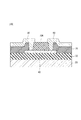
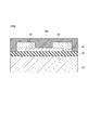
酸化物焼結体の形状は特に限定されないが、図1の符号1に示すような板状でもよく、図2の符号1Aに示すような円筒状でもよい。板状の場合、平面形状は、図1の符号1に示すような矩形でもよく、図3の符号1Bに示すように円形でもよい。酸化物焼結体は一体成型でもよく、図4に示すように、複数に分割した酸化物焼結体(符号1C)をバッキングプレート3に各々固定した多分割式でもよい。
バッキングプレート3は、酸化物焼結体の保持や冷却用の部材である。材料は銅等の熱伝導性に優れた材料が好ましい。The shape of the oxide sintered body is not particularly limited, but it may be a plate shape as shown by reference numeral 1 in FIG. 1 or a cylindrical shape as shown by
The
スパッタリングターゲットは、例えば以下の工程で製造される。
酸化物焼結体の表面を研削する工程(研削工程)。
酸化物焼結体をバッキングプレートにボンディングする工程(ボンディング工程)。
以下、各工程を具体的に説明する。The sputtering target is manufactured, for example, by the following steps.
The process of grinding the surface of an oxide sintered body (grinding process).
A process of bonding an oxide sintered body to a backing plate (bonding process).
Hereinafter, each step will be specifically described.
<研削工程>
研削工程では、焼結体を、スパッタリング装置への装着に適した形状に切削加工する。
焼結体表面は、高酸化状態の焼結部が存在したり、面が凸凹であることが多く、また、所定の寸法に切断加工する必要がある。
焼結体の表面は0.3mm以上研削するのが好ましい。研削する深さは、0.5mm以上研削するのが好ましく、2mm以上が特に好ましい。0.3mm以上研削することにより、表面付近の結晶構造の変動部分を除去できる。<Grinding process>
In the grinding process, the sintered body is cut into a shape suitable for mounting on a sputtering apparatus.
The surface of the sintered body often has a highly oxidized sintered portion or has an uneven surface, and needs to be cut to a predetermined size.
The surface of the sintered body is preferably ground by 0.3 mm or more. The grinding depth is preferably 0.5 mm or more, and particularly preferably 2 mm or more. By grinding 0.3 mm or more, the fluctuating part of the crystal structure near the surface can be removed.
酸化物焼結体を例えば、平面研削盤で研削して平均表面粗さRaが5μm以下の素材とするのが好ましい。さらにスパッタリングターゲットのスパッタ面に鏡面加工を施して、平均表面粗さRaが1000×10-10m以下としてもよい。鏡面加工(研磨)は、機械的な研磨、化学研磨、およびメカノケミカル研磨(機械的な研磨と化学研磨の併用)等の、公知の研磨技術を用いることができる。例えば、固定砥粒ポリッシャー(ポリッシュ液は水)で#2000番以上にポリッシングしてもよく、遊離砥粒ラップ(研磨材はSiCペースト等)にてラッピング後、研磨材をダイヤモンドペーストに換えて、ラッピングしてもよい。研磨方法はこれらの方法に限定されない。研磨材は、#200番、もしくは#400番、さらには#800番のものが挙げられる。For example, it is preferable to grind the oxide sintered body with a surface grinding machine to obtain a material having an average surface roughness Ra of 5 μm or less. Further, the sputtered surface of the sputtering target may be mirror-finished so that the average surface roughness Ra is 1000 × 10 -10 m or less. For mirror polishing (polishing), known polishing techniques such as mechanical polishing, chemical polishing, and mechanochemical polishing (combination of mechanical polishing and chemical polishing) can be used. For example, it may be polished to # 2000 or higher with a fixed abrasive grain polisher (polishing liquid is water), wrapped with free abrasive grain wrap (abrasive material is SiC paste, etc.), and then the abrasive material is changed to diamond paste. You may wrap it. The polishing method is not limited to these methods. Examples of the abrasive material include # 200, # 400, and even # 800.
研削工程後の酸化物焼結体は、エアーブローや流水洗浄等で清浄するのが好ましい。エアーブローで異物を除去する際には、ノズルの向い側から集塵機で吸気を行なうとより有効に除去できる。なお、エアーブローや流水洗浄では清浄力に限界があるので、さらに超音波洗浄等を行なうこともできる。超音波洗浄は、周波数が25kHz以上、300kHz以下の間で、多重発振させて行なう方法が有効である。例えば周波数が25kHz以上、300kHzの間で、25kHz刻みに12種類の周波数を多重発振させて、超音波洗浄を行なうのが良い。 The oxide sintered body after the grinding step is preferably cleaned by air blowing, running water washing, or the like. When removing foreign matter with an air blow, it can be removed more effectively by sucking air with a dust collector from the opposite side of the nozzle. Since there is a limit to the cleaning power of air blow and running water cleaning, ultrasonic cleaning and the like can be further performed. It is effective to perform ultrasonic cleaning by oscillating multiple times between frequencies of 25 kHz or more and 300 kHz or less. For example, it is preferable to perform ultrasonic cleaning by oscillating 12 kinds of frequencies in 25 kHz increments between frequencies of 25 kHz or more and 300 kHz.
<ボンディング工程>
ボンディング工程では、研削後の焼結体を、金属インジウムなどの低融点金属で、バッキングプレートにボンディングする。
以上がスパッタリングターゲットの説明である。<Bonding process>
In the bonding step, the ground sintered body is bonded to the backing plate with a low melting point metal such as metallic indium.
The above is the description of the sputtering target.
[酸化物半導体膜]
本発明の一態様の酸化物半導体膜(以下、本発明の半導体膜と略称することがある)は、In、Ga及びSnを下記原子比
0.01≦Ga/(In+Ga+Sn)≦0.30 ・・・(1)
0.01≦Sn/(In+Ga+Sn)≦0.40 ・・・(2)
0.55≦In/(In+Ga+Sn)≦0.98 ・・・(3)で含有し、
かつ、レアアース元素Xを下記原子比
0.03≦X/(In+Ga+Sn+X)≦0.25 ・・・(4)
で含有することを特徴とする。
本発明の半導体膜は、薄膜トランジスタの半導体層(半導体部分)として好適に用いることができる。[Oxide semiconductor film]
The oxide semiconductor film of one aspect of the present invention (hereinafter, may be abbreviated as the semiconductor film of the present invention) has In, Ga and Sn having the following atomic ratios of 0.01 ≦ Ga / (In + Ga + Sn) ≦ 0.30.・ ・ (1)
0.01 ≤ Sn / (In + Ga + Sn) ≤ 0.40 ... (2)
0.55 ≤ In / (In + Ga + Sn) ≤ 0.98 ... (3)
And the rare earth element X has the following atomic ratio 0.03 ≤ X / (In + Ga + Sn + X) ≤ 0.25 ... (4)
It is characterized by being contained in.
The semiconductor film of the present invention can be suitably used as a semiconductor layer (semiconductor portion) of a thin film transistor.
上記原子比組成を有する本発明の半導体膜は、同じ原子比組成を有する上記本発明のスパッタリングターゲットを、スパッタすることによって形成することができる。
酸化物焼結体からなるスパッタリングターゲットを、スパッタして形成された膜の原子比組成は、用いたスパッタリングターゲットの原子比組成と一致する。The semiconductor film of the present invention having the above atomic ratio composition can be formed by sputtering the sputtering target of the present invention having the same atomic ratio composition.
The atomic ratio composition of the film formed by sputtering a sputtering target made of an oxide sintered body matches the atomic ratio composition of the sputtering target used.
スパッタ法としては、DCスパッタ法、RFスパッタ法、パルスDCスパッタ法等が好適に使用できる。パルスDCスパッタ法の場合、10kHz〜300kHzのパルスにて、デューティー比20〜90%にて成膜することができる。出力は成膜速度の関数であり、得たい成膜速度に合わせて調整すればよい。 As the sputtering method, a DC sputtering method, an RF sputtering method, a pulse DC sputtering method and the like can be preferably used. In the case of the pulse DC sputtering method, a film can be formed with a pulse of 10 kHz to 300 kHz at a duty ratio of 20 to 90%. The output is a function of the film formation rate, and may be adjusted according to the desired film formation rate.
本発明の一実施形態の半導体膜は、スパッタによって成膜されたときにアモルファス状態であり、加熱処理(アニール処理)後もアモルファス状態であることが好ましい。酸化インジウム結晶が生成すると、その結晶にスズがドーピングされITOと同様に導電化する場合がある。酸化インジウム結晶が微結晶の場合は、アモルファス状の部分と微結晶が混在することになり、それらの界面でキャリヤーが散乱され移動度が低下する場合がある。また、アモルファス状の部分と微結晶の間に酸素欠損等が生じると、光吸収の色中心を生成する場合があり、TFTの光安定性が損なわれる場合がある。 The semiconductor film of one embodiment of the present invention is preferably in an amorphous state when it is formed by sputtering, and is preferably in an amorphous state even after heat treatment (annealing treatment). When indium oxide crystals are formed, tin may be doped into the crystals to make them conductive in the same manner as ITO. When the indium oxide crystal is a microcrystal, the amorphous portion and the microcrystal are mixed, and carriers may be scattered at the interface between them to reduce the mobility. Further, if oxygen deficiency or the like occurs between the amorphous portion and the microcrystal, a color center of light absorption may be generated, and the light stability of the TFT may be impaired.
酸化物半導体膜の原子比組成が上記範囲以外では、薄膜トランジスタを形成する工程で使用されるCVD成膜装置での処理の際に、薄膜トランジスタの半導体部分(本発明の半導体膜)のキャリヤー濃度が上昇し、その後のアニール処理によってもキャリヤー濃度が低下せず、TFTとして作動しなくなる場合があった。そのため、CVD装置の成膜温度を低下させて、キャリヤー濃度の上昇を抑え、TFT特性の発現を行っていたが、CVD装置の成膜温度を低減させたことにより、耐久性の乏しい半導体膜しか得られず、TFT特性も劣ったものとなる場合がある。 When the atomic ratio composition of the oxide semiconductor film is outside the above range, the carrier concentration of the semiconductor portion (semiconductor film of the present invention) of the thin film transistor increases during processing with the CVD film forming apparatus used in the step of forming the thin film transistor. However, the carrier concentration did not decrease even after the subsequent annealing treatment, and the TFT may not operate. Therefore, the film formation temperature of the CVD device is lowered to suppress the increase in the carrier concentration, and the TFT characteristics are exhibited. However, by reducing the film formation temperature of the CVD device, only the semiconductor film having poor durability is used. It may not be obtained and the TFT characteristics may be inferior.
本発明の半導体膜において、酸化ガリウムは、酸素欠損の発生を抑える効果と、酸化物半導体膜のバンドギャップを大きくする効果が有る。Gaの割合[Ga/(In+Ga+Sn)(原子比)]は、0.01≦Ga/(In+Ga+Sn)≦0.30であることが好ましい。0.01未満では、酸素欠損を抑える効果が小さく、半導体膜にならない場合がある。また、0.30超では、酸素欠損がなくなり、絶縁膜となる場合があった。より好ましくは、0.02≦Ga/(In+Ga+Sn)≦0.25、さらに好ましくは、0.03≦Ga/(In+Ga+Sn)≦0.20である。 In the semiconductor film of the present invention, gallium oxide has an effect of suppressing the occurrence of oxygen deficiency and an effect of increasing the band gap of the oxide semiconductor film. The ratio of Ga [Ga / (In + Ga + Sn) (atomic ratio)] is preferably 0.01 ≦ Ga / (In + Ga + Sn) ≦ 0.30. If it is less than 0.01, the effect of suppressing oxygen deficiency is small, and the semiconductor film may not be formed. Further, when it exceeds 0.30, oxygen deficiency disappears and an insulating film may be formed. More preferably, 0.02 ≦ Ga / (In + Ga + Sn) ≦ 0.25, and even more preferably 0.03 ≦ Ga / (In + Ga + Sn) ≦ 0.20.
本発明の半導体膜において、酸化スズは、耐薬品性を有しており、かつ導電膜として使用されることからもわかるように、半導体膜の移動度に影響を及ぼすことは少ないと考えられる。よって、Snの割合[Sn/(In+Ga+Sn)(原子比)]は、0.01≦Sn/(In+Ga+Sn)≦0.40が好ましい。0.01未満では、耐薬品性が得られない場合がある。0.40超では、耐薬品性が高すぎて、エッチングによる半導体膜のアイランド形成ができない場合がある。より好ましくは、0.02≦Sn/(In+Ga+Sn)≦0.35、さらに好ましくは0.03≦Sn/(In+Ga+Sn)≦0.30である。 In the semiconductor film of the present invention, tin oxide has chemical resistance and is considered to have little effect on the mobility of the semiconductor film, as can be seen from the fact that it is used as a conductive film. Therefore, the ratio of Sn [Sn / (In + Ga + Sn) (atomic ratio)] is preferably 0.01 ≦ Sn / (In + Ga + Sn) ≦ 0.40. If it is less than 0.01, chemical resistance may not be obtained. If it exceeds 0.40, the chemical resistance is too high, and island formation of the semiconductor film by etching may not be possible. More preferably, 0.02 ≦ Sn / (In + Ga + Sn) ≦ 0.35, and even more preferably 0.03 ≦ Sn / (In + Ga + Sn) ≦ 0.30.
本発明の半導体膜において、酸化インジウムは、半導体膜の移動度を担う酸化物である。Inの割合[In/(In+Ga+Sn)(原子比)]は、0.55≦In/(In+Ga+Sn)≦0.98が好ましい。0.55未満では、半導体膜の移動度の低下が起こる場合がある。0.98以上では、半導体膜が結晶化したり、酸素欠損の量が増えすぎて、半導体化せず、導体になる場合がある。より好ましくは、0.60≦In/(In+Ga+Sn)≦0.96、さらに好ましくは、0.60≦In/(In+Ga+Sn)≦0.94である。 In the semiconductor film of the present invention, indium oxide is an oxide responsible for the mobility of the semiconductor film. The ratio of In [In / (In + Ga + Sn) (atomic ratio)] is preferably 0.55 ≦ In / (In + Ga + Sn) ≦ 0.98. If it is less than 0.55, the mobility of the semiconductor film may decrease. If it is 0.98 or more, the semiconductor film may crystallize or the amount of oxygen deficiency may increase too much to become a conductor without becoming a semiconductor. More preferably, 0.60 ≦ In / (In + Ga + Sn) ≦ 0.96, and even more preferably 0.60 ≦ In / (In + Ga + Sn) ≦ 0.94.
本発明の半導体膜において、レアアース元素Xの酸化物は、半導体膜を非晶質化する作用と、酸素欠損によるキャリャーの発生を抑える作用を有する。ベースの原料酸化物における酸化インジウムの割合が多い酸化物半導体膜の場合、レアアース元素Xの酸化物の量を比較的多くしないと半導体膜が結晶化してしまったり、結晶化による酸化スズのドーパント効果によるキャリヤーの増大や、アモルファス状態での酸素欠損によるキャリヤーの増大を抑えることができなくなる。一方、ベースの原料酸化物における酸化インジウムの割合が少ない酸化物半導体膜の場合、レアアース元素Xの酸化物の量を比較的少なくしないと、膜が絶縁化したり、当該酸化物半導体膜を用いた薄膜トランジスタの移動度が低下したりする場合が有る。ベースの原料酸化物におけるInの割合に合わせて、レアアース元素Xの割合を適宜調整すればよい。 In the semiconductor film of the present invention, the oxide of the rare earth element X has an action of amorphizing the semiconductor film and an action of suppressing the generation of carriers due to oxygen deficiency. In the case of an oxide semiconductor film in which the proportion of indium oxide in the base raw material oxide is large, the semiconductor film may crystallize unless the amount of oxide of the rare earth element X is relatively large, or the dopant effect of tin oxide due to crystallization. It becomes impossible to suppress the increase of carriers due to the above-mentioned increase and the increase of carriers due to oxygen deficiency in the amorphous state. On the other hand, in the case of an oxide semiconductor film in which the proportion of indium oxide in the base raw material oxide is small, the film is insulated or the oxide semiconductor film is used unless the amount of the oxide of the rare earth element X is relatively small. The mobility of the thin film transistor may decrease. The ratio of the rare earth element X may be appropriately adjusted according to the ratio of In in the base raw material oxide.
例えば、Inの割合[In/(In+Ga+Sn)(原子比)]が0.85以上の場合には、レアアース元素Xの割合[X/(In+Ga+Sn+X)(原子比)]は、0.03以上、好ましくは、0.04以上が好ましく、より好ましくは0.05以上であり、上限は0.25以下であることが好ましい。Inの割合[In/(In+Ga+Sn)(原子比)]が0.85以上では、半導体膜が結晶化しやすくなる場合があり、その結晶化を抑えるためにレアアース元素Xの添加量を増量することが好ましい。また、酸化インジウムの酸素欠損量もInの割合の増大に従って増大するので、キャリヤー発生を抑えるためにも、半導体膜中のレアアース元素Xの添加量を増加させることが好ましい。 For example, when the ratio of In [In / (In + Ga + Sn) (atomic ratio)] is 0.85 or more, the ratio of rare earth element X [X / (In + Ga + Sn + X) (atomic ratio)] is preferably 0.03 or more. Is preferably 0.04 or more, more preferably 0.05 or more, and the upper limit is preferably 0.25 or less. When the ratio of In [In / (In + Ga + Sn) (atomic ratio)] is 0.85 or more, the semiconductor film may easily crystallize, and the amount of the rare earth element X added may be increased in order to suppress the crystallization. preferable. Further, since the oxygen deficiency amount of indium oxide also increases as the proportion of In increases, it is preferable to increase the addition amount of the rare earth element X in the semiconductor film in order to suppress the generation of carriers.
また、Inの割合[In/(In+Ga+Sn)(原子比)]が0.70以下の場合は、添加するレアアース元素Xの割合[X/(In+Ga+Sn+X)(原子比)]を0.25以下とすることが好ましく、より好ましくは0.20以下にする。より好ましくは0.17以下である。下限は0.03以上であることが好ましい。
レアアース元素Xは、酸素欠損によるキャリヤーの発生を抑える効果が大きく、例えば、ケミカルベーパーデポジション(CVD)処理等により、層間絶縁膜やゲート絶縁膜の形成時に半導体膜に発生するキャリヤーを、後アニール時に正常なキャリヤー濃度に戻す能力が高い。レアアース元素Xのこの性質により、CVD処理等により一旦はキャリヤー濃度が高くなっても、後アニールにより膜が半導体として機能し得る正常なキャリヤー濃度に戻り、TFT特性を回復することができることが分かった。When the ratio of In [In / (In + Ga + Sn) (atomic ratio)] is 0.70 or less, the ratio of rare earth element X to be added [X / (In + Ga + Sn + X) (atomic ratio)] is set to 0.25 or less. It is preferably 0.20 or less, more preferably 0.20 or less. More preferably, it is 0.17 or less. The lower limit is preferably 0.03 or more.
The rare earth element X has a large effect of suppressing the generation of carriers due to oxygen deficiency. For example, the carriers generated in the semiconductor film when the interlayer insulating film or the gate insulating film is formed by chemical vapor deposition (CVD) treatment or the like are post-annealed. High ability to return to normal carrier concentration at times. It was found that due to this property of the rare earth element X, even if the carrier concentration is once increased by CVD treatment or the like, the film can return to the normal carrier concentration capable of functioning as a semiconductor by post-annealing, and the TFT characteristics can be restored. ..
Inの割合[In/(In+Ga+Sn)(原子比)]が上記の中間の、0.70超0.85未満の場合は、成膜の条件(酸素濃度、基板温度、成膜圧力、背圧等)を適宜選択すればよい。Inの割合[In/(In+Ga+Sn)(原子比)]が上記の中間の、0.70超0.85未満の場合において、Gaの割合[Ga/(In+Ga+Sn)(原子比)]が0.10を超える場合は、酸化ガリウムのアモルファス化効果、及びキャリヤーの制御効果が発現するので、レアアース元素Xの割合[X/(In+Ga+Sn+X)(原子比)]は、Inの割合[In/(In+Ga+Sn)(原子比)]が0.85以上の場合ほどの量は必要ないが、半導体膜の用途により耐CVD性等を持たせたい場合や、半導体膜の耐久性をより向上させたい場合には、Inの割合[In/(In+Ga+Sn)(原子比)]が0.85以上の場合と同じ程度の量を添加すればよい。 When the ratio of In [In / (In + Ga + Sn) (atomic ratio)] is in the middle of the above, more than 0.70 and less than 0.85, the conditions for film formation (oxygen concentration, substrate temperature, film formation pressure, back pressure, etc.) ) May be selected as appropriate. When the ratio of In [In / (In + Ga + Sn) (atomic ratio)] is in the middle of the above, more than 0.70 and less than 0.85, the ratio of Ga [Ga / (In + Ga + Sn) (atomic ratio)] is 0.10. If it exceeds, the amorphization effect of gallium oxide and the control effect of the carrier are exhibited. Therefore, the ratio of rare earth element X [X / (In + Ga + Sn + X) (atomic ratio)] is the ratio of In [In / (In + Ga + Sn) ( Atomic ratio)] is not required as much as when it is 0.85 or more, but if you want to have CVD resistance etc. depending on the application of the semiconductor film, or if you want to further improve the durability of the semiconductor film, In The amount of the ratio [In / (In + Ga + Sn) (atomic ratio)] of 0.85 or more may be added in the same amount as in the case of 0.85 or more.
一方、Snの割合[Sn/(In+Ga+Sn)(原子比)]が0.20を超える場合は、耐薬品性が非常に高くなるので、エッチングプロセス等に耐性のある半導体膜が得られる。さらにCVD耐性や、TFTの耐久性を考慮してXの割合を適宜選択すればよい。一方で、本発明の半導体膜を、薄膜トランジスタの移動度の高い用途に適用する場合には、Inの割合[In/(In+Ga+Sn)(原子比)]が0.85以下の場合の、レアアース元素Xの割合[X/(In+Ga+Sn+X)(原子比)]を減らすことができる。これにより、移動度が高い酸化物半導体膜を用いた、薄膜トランジスタを提供することができるようになる。 On the other hand, when the Sn ratio [Sn / (In + Ga + Sn) (atomic ratio)] exceeds 0.20, the chemical resistance becomes very high, so that a semiconductor film resistant to an etching process or the like can be obtained. Further, the ratio of X may be appropriately selected in consideration of CVD resistance and TFT durability. On the other hand, when the semiconductor film of the present invention is applied to a high mobility application of a thin film transistor, the rare earth element X when the ratio of In [In / (In + Ga + Sn) (atomic ratio)] is 0.85 or less. [X / (In + Ga + Sn + X) (atomic ratio)] can be reduced. This makes it possible to provide a thin film transistor using an oxide semiconductor film having high mobility.
また、酸化ガリウム及び/又はレアアース元素Xの酸化物の添加は、酸化物半導体膜のバンドギャップを向上させる効果が有り、光耐性の高い酸化物半導体膜及び薄膜トランジスタ(TFT)を得やすくなる。酸化ガリウムとレアアース元素Xの酸化物の量は、酸素欠損量とも密接に関係しているので、得られる半導体膜の用途に応じた耐久性の要望に合わせて適宜選択すればよい。 Further, the addition of an oxide of gallium oxide and / or the rare earth element X has an effect of improving the band gap of the oxide semiconductor film, and makes it easy to obtain an oxide semiconductor film and a thin film transistor (TFT) having high photoresistance. Since the amounts of gallium oxide and the oxides of the rare earth element X are closely related to the amount of oxygen deficiency, they may be appropriately selected according to the demand for durability according to the application of the obtained semiconductor film.
本発明の一実施形態の酸化物半導体膜は、In、Ga及びSnを下記原子比
0.02≦Ga/(In+Ga+Sn)≦0.25 ・・・(1A)
0.02≦Sn/(In+Ga+Sn)≦0.35 ・・・(2A)
0.60≦In/(In+Ga+Sn)≦0.96 ・・・(3A)
で含有し、
かつ、レアアース元素Xを下記原子比
0.03≦X/(In+Ga+Sn+X)≦0.25 ・・・(4A)
で含有することが好ましい。In the oxide semiconductor film of one embodiment of the present invention, In, Ga and Sn have the following atomic ratios of 0.02 ≦ Ga / (In + Ga + Sn) ≦ 0.25 ... (1A)
0.02 ≤ Sn / (In + Ga + Sn) ≤ 0.35 ... (2A)
0.60 ≤ In / (In + Ga + Sn) ≤ 0.96 ... (3A)
Contained in
And the rare earth element X has the following atomic ratio 0.03 ≤ X / (In + Ga + Sn + X) ≤ 0.25 ... (4A)
It is preferable to contain in.
本発明の一実施形態の酸化物半導体膜は、In、Ga及びSnを下記原子比
0.03≦Ga/(In+Ga+Sn)≦0.20 ・・・(1B)
0.03≦Sn/(In+Ga+Sn)≦0.30 ・・・(2B)
0.60≦In/(In+Ga+Sn)≦0.94 ・・・(3B)
で含有し、
かつ、レアアース元素Xを下記原子比
0.03≦X/(In+Ga+Sn+X)≦0.25 ・・・(4B)
で含有することがより好ましい。In the oxide semiconductor film of one embodiment of the present invention, In, Ga and Sn have the following atomic ratios of 0.03 ≦ Ga / (In + Ga + Sn) ≦ 0.20 ... (1B)
0.03 ≤ Sn / (In + Ga + Sn) ≤ 0.30 ... (2B)
0.60 ≤ In / (In + Ga + Sn) ≤ 0.94 ... (3B)
Contained in
And the rare earth element X has the following atomic ratio 0.03 ≤ X / (In + Ga + Sn + X) ≤ 0.25 ... (4B)
It is more preferable to contain in.
酸化物半導体膜は、レアアース元素のうち、イットリウム(Y)、ランタン(La)、ネオジム(Nd)、サマリウム(Sm)、ユウロピウム(Eu)、ガドリニウム(Gd)、テルビウム(Tb)、ジスプロシウム(Dy)、ホロミウム(Ho)、エルビウム(Er)、ツリウム(Tm)、イッテルビウム(Yb)及びルテチウム(Lu)からなる群から選択される、1種以上を用いることが好ましく、イットリウム(Y)、サマリウム(Sm)及びイッテルビウム(Yb)からなる群から選択される1種以上を用いることが、さらに好ましい。
レアアース元素Xは、イットリウム(Y)、ランタン(La)、ネオジム(Nd)及びサマリウム(Sm)からなる群から選択される1種以上であるのが、よりさらに好ましい。Among the rare earth elements, the oxide semiconductor film includes yttrium (Y), lanthanum (La), neodymium (Nd), samarium (Sm), europium (Eu), gadrinium (Gd), terbium (Tb), and disprosium (Dy). , Holmium (Ho), Elbium (Er), Yttrium (Tm), Ytterbium (Yb) and Lutetium (Lu). ) And ytterbium (Yb), it is more preferable to use one or more selected from the group.
It is even more preferable that the rare earth element X is one or more selected from the group consisting of yttrium (Y), lanthanum (La), neodymium (Nd) and samarium (Sm).
酸化物半導体膜中の各金属元素の含有量(原子比)は、ICP(Inductive Coupled Plasma)測定またはXRF(X−rayFluorescence)測定により、各元素の存在量を測定することで求めることができる。ICP測定は誘導プラズマ発光分析装置を用いることができる。XRF測定は薄膜蛍光X線分析装置(AZX400、リガク社製)を用いることができる。 The content (atomic ratio) of each metal element in the oxide semiconductor film can be determined by measuring the abundance of each element by ICP (Inductive Coupled Plasma) measurement or XRF (X-ray Fluorescence) measurement. An inductively coupled plasma emission spectrometer can be used for ICP measurement. A thin film fluorescent X-ray analyzer (AZX400, manufactured by Rigaku Corporation) can be used for the XRF measurement.
また、セクタ型ダイナミック二次イオン質量分析計SIMS分析を用いても誘導プラズマ発光分析と同等の精度で酸化物半導体薄膜中の各金属元素の含有量(原子比)を分析できる。誘導プラズマ発光分析装置または薄膜蛍光X線分析装置で測定した金属元素の原子比が既知の標準酸化物薄膜の上面に、ソース・ドレイン電極をTFT素子と同様の材料をチャネル長で形成したものを標準材料とし、セクタ型ダイナミック二次イオン質量分析計SIMS(IMS 7f−Auto、AMETEK社製)により酸化物半導体層の分析に行い各元素の質量スペクトル強度を得、既知の元素濃度と質量スペクトル強度の検量線を作製する。次に、実TFT素子の酸化物半導体膜部分を、セクタ型ダイナミック二次イオン質量分析計SIMS分析によるスペクトル強度から、前述の検量線を用いて、原子比を算出すると、算出された原子比は、別途薄膜蛍光X線分析装置または誘導プラズマ発光分析装置で測定された酸化物半導体膜の原子比の2原子%以内であることが確認できる。 Further, the content (atomic ratio) of each metal element in the oxide semiconductor thin film can be analyzed with the same accuracy as inductively coupled plasma emission spectrometry by using the sector type dynamic secondary ion mass spectrometer SIMS analysis. A source / drain electrode formed of the same material as the TFT element with a channel length on the upper surface of a standard oxide thin film whose atomic ratio of metal elements is known as measured by an inductive plasma emission analyzer or a thin film fluorescent X-ray analyzer. Using a sector-type dynamic secondary ion mass spectrometer SIMS (IMS 7f-Auto, manufactured by AMETEK) as a standard material, the oxide semiconductor layer was analyzed to obtain the mass spectral intensity of each element, and the known element concentration and mass spectral intensity were obtained. Make a calibration line of. Next, when the atomic ratio of the oxide semiconductor film portion of the actual TFT element is calculated from the spectral intensity by the sector type dynamic secondary ion mass spectrometer SIMS analysis using the above-mentioned calibration line, the calculated atomic ratio is calculated. It can be confirmed that the atomic ratio of the oxide semiconductor film is within 2 atomic% separately measured by a thin film fluorescent X-ray analyzer or an induced plasma emission analyzer.
[薄膜トランジスタ]
本発明の一態様の薄膜トランジスタ(以下、本発明のTFTと略称することがある)は、上記本発明の酸化物半導体膜を用いたことを特徴とする。
本発明の一実施形態の薄膜トランジスタの形状は、特に限定されないが、バックチャンネルエッチ型トランジスタ、エッチストッパー型トランジスタ、トップゲート型トランジスタ等が好ましい。
本発明の一実施形態に係る非晶質酸化物半導体膜は薄膜トランジスタに用いることができ、薄膜トランジスタのチャネル層として好適である。
本発明の一実施形態に係る薄膜トランジスタは、本発明の一実施形態に係る非晶質酸化物半導体膜を、チャネル層として有していれば他の素子構成は特に限定されず、公知のものを採用することができる。本発明の薄膜トランジスタは、液晶ディスプレイや有機ELディスプレイ等の表示装置に好適に用いることができる。[Thin film transistor]
The thin film transistor of one aspect of the present invention (hereinafter, may be abbreviated as the TFT of the present invention) is characterized in that the oxide semiconductor film of the present invention is used.
The shape of the thin film transistor according to the embodiment of the present invention is not particularly limited, but a back channel etch type transistor, an etch stopper type transistor, a top gate type transistor and the like are preferable.
The amorphous oxide semiconductor film according to the embodiment of the present invention can be used for a thin film transistor and is suitable as a channel layer for the thin film transistor.
The thin film transistor according to the embodiment of the present invention is not particularly limited in other element configurations as long as it has the amorphous oxide semiconductor film according to the embodiment of the present invention as a channel layer, and known ones are used. Can be adopted. The thin film of the present invention can be suitably used for display devices such as liquid crystal displays and organic EL displays.
本発明の一実施形態に係る薄膜トランジスタにおけるチャネル層の膜厚は、通常10〜300nm、好ましくは20〜250nmである。 The film thickness of the channel layer in the thin film transistor according to the embodiment of the present invention is usually 10 to 300 nm, preferably 20 to 250 nm.
本発明の一実施形態に係る薄膜トランジスタにおけるチャネル層は、通常、N型領域で用いられるが、P型Si系半導体、P型酸化物半導体、P型有機半導体等の種々のP型半導体と組合せて、PN接合型トランジスタ等の各種の半導体デバイスに利用することができる。 The channel layer in the thin film according to the embodiment of the present invention is usually used in the N-type region, but is combined with various P-type semiconductors such as P-type Si-based semiconductors, P-type oxide semiconductors, and P-type organic semiconductors. It can be used for various semiconductor devices such as PN junction type transistors.
本発明の一実施形態に係る薄膜トランジスタは、電界効果型トランジスタ、論理回路、メモリ回路、差動増幅回路等各種の集積回路にも適用できる。さらに、電界効果型トランジスタ以外にも静電誘起型トランジスタ、ショットキー障壁型トランジスタ、ショットキーダイオード、抵抗素子にも適応できる。 The thin film transistor according to an embodiment of the present invention can also be applied to various integrated circuits such as field effect transistors, logic circuits, memory circuits, and differential amplifier circuits. Further, in addition to the field effect transistor, it can be applied to an electrostatic induction transistor, a Schottky barrier transistor, a Schottky diode, and a resistance element.
本発明の一実施形態に係る薄膜トランジスタの構成は、ボトムゲート、ボトムコンタクト、トップコンタクト等公知の構成を制限なく採用することができる。
特にボトムゲート構成が、アモルファスシリコンやZnOの薄膜トランジスタに比べ、高い性能が得られるので有利である。ボトムゲート構成は、製造時のマスク枚数を削減しやすく、大型ディスプレイ等の用途の製造コストを低減しやすいため好ましい。
本発明の一実施形態に係る薄膜トランジスタは、表示装置に好適に用いることができる。As the configuration of the thin film transistor according to the embodiment of the present invention, known configurations such as a bottom gate, a bottom contact, and a top contact can be adopted without limitation.
In particular, the bottom gate configuration is advantageous because high performance can be obtained as compared with the thin film transistor of amorphous silicon or ZnO. The bottom gate configuration is preferable because it is easy to reduce the number of masks during manufacturing and it is easy to reduce the manufacturing cost for applications such as large displays.
The thin film transistor according to the embodiment of the present invention can be suitably used for a display device.
大面積のディスプレイ用としては、チャンネルエッチ型のボトムゲート構成の薄膜トランジスタが特に好ましい。チャンネルエッチ型のボトムゲート構成の薄膜トランジスタは、フォトリソ工程時のフォトマスクの数が少なく、低コストでディスプレイ用パネルを製造できる。中でも、チャンネルエッチ型のボトムゲート構成、及びトップコンタクト構成の薄膜トランジスタが、移動度等の特性が良好で工業化しやすいため特に好ましい。 For a large-area display, a thin film transistor having a channel-etched bottom gate configuration is particularly preferable. The thin film transistor having a channel-etched bottom gate configuration has a small number of photomasks in the photolithography process, and can manufacture a display panel at low cost. Among them, a thin film transistor having a channel etch type bottom gate configuration and a top contact configuration is particularly preferable because it has good characteristics such as mobility and is easy to industrialize.
具体的な薄膜トランジスタの例を図5および図6に示す。
図5に示すように、薄膜トランジスタ100は、シリコンウエハ20、ゲート絶縁膜30、酸化物半導体薄膜40、ソース電極50、ドレイン電極60、および層間絶縁膜70、70Aを備える。Specific examples of the thin film transistor are shown in FIGS. 5 and 6.
As shown in FIG. 5, the
シリコンウエハ20はゲート電極である。ゲート絶縁膜30はゲート電極と酸化物半導体薄膜40の導通を遮断する絶縁膜であり、シリコンウエハ20上に設けられる。
酸化物半導体薄膜40はチャネル層であり、ゲート絶縁膜30上に設けられる。酸化物半導体薄膜40は本発明の一実施形態に係る酸化物半導体薄膜が用いられる。The
The oxide semiconductor
ソース電極50およびドレイン電極60は、ソース電流およびドレイン電流を酸化物半導体薄膜40に流すための導電端子であり、酸化物半導体薄膜40の両端近傍に接触するように、各々設けられる。
層間絶縁膜70は、ソース電極50およびドレイン電極60と、酸化物半導体薄膜40の間の接触部分以外の導通を遮断する絶縁膜である。
層間絶縁膜70Aは、ソース電極50およびドレイン電極60と、酸化物半導体薄膜40の間の接触部分以外の導通を遮断する絶縁膜である。層間絶縁膜70Aは、ソース電極50とドレイン電極60の間の導通を遮断する絶縁膜でもある。層間絶縁膜70Aは、チャネル層保護層でもある。The
The
The
図5に示すように、薄膜トランジスタ100Aの構造は、薄膜トランジスタ100と同様であるが、ソース電極50およびドレイン電極60を、ゲート絶縁膜30と酸化物半導体薄膜40の両方に接触するように設けている点が異なる。ゲート絶縁膜30、酸化物半導体薄膜40、ソース電極50、およびドレイン電極60を覆うように、層間絶縁膜70Bが一体に設けられている点も異なる。
As shown in FIG. 5, the structure of the
ドレイン電極60、ソース電極50およびゲート電極を形成する材料に特に制限はなく、一般に用いられている材料を任意に選択することができる。図5および図6で挙げた例では、シリコンウエハを基板として用いており、シリコンウエハが電極としても作用するが、電極材料はシリコンに限定されない。
例えば、酸化インジウムスズ(ITO)、酸化インジウム亜鉛(IZO)、ZnO、およびSnO2等の透明電極や、Al、Ag、Cu、Cr、Ni、Mo、Au、Ti、およびTa等の金属電極、またはこれらを含む合金の金属電極や積層電極を用いることができる。
また、図5および図6において、ガラス等の基板上にゲート電極を形成してもよい。The material forming the
For example, transparent electrodes such as indium tin oxide (ITO), zinc oxide (IZO), ZnO, and SnO 2 , and metal electrodes such as Al, Ag, Cu, Cr, Ni, Mo, Au, Ti, and Ta. Alternatively, a metal electrode or a laminated electrode of an alloy containing these can be used.
Further, in FIGS. 5 and 6, the gate electrode may be formed on a substrate such as glass.
層間絶縁膜70、70A、70Bを形成する材料にも特に制限はなく、一般に用いられている材料を任意に選択できる。層間絶縁膜70、70A、70Bを形成する材料として、具体的には、例えば、SiO2、SiNx、Al2O3、Ta2O5、TiO2、MgO、ZrO2、CeO2、K2O、Li2O、Na2O、Rb2O、Sc2O3、Y2O3、HfO2、CaHfO3、PbTiO3、BaTa2O6、SrTiO3、Sm2O3、およびAlN等の化合物を用いることができる。The material forming the interlayer insulating
本発明の一実施形態に係る薄膜トランジスタが、バックチャネルエッチ型(ボトムゲート型)の場合、ドレイン電極、ソース電極およびチャネル層上に保護膜を設けることが好ましい。保護膜を設けることにより、TFTの長時間駆動した場合でも耐久性が向上しやすくなる。なお、トップゲート型のTFTの場合、例えばチャネル層上にゲート絶縁膜を形成した構造となる。 When the thin film transistor according to the embodiment of the present invention is a back channel etch type (bottom gate type), it is preferable to provide a protective film on the drain electrode, the source electrode and the channel layer. By providing the protective film, the durability can be easily improved even when the TFT is driven for a long time. In the case of a top gate type TFT, for example, the structure is such that a gate insulating film is formed on the channel layer.
保護膜または絶縁膜は、例えばCVDにより形成することができるが、その際に高温度によるプロセスになる場合がある。また、保護膜または絶縁膜は、成膜直後は不純物ガスを含有していることが多く、加熱処理(アニール処理)を行うことが好ましい。加熱処理で不純物ガスを取り除くことにより、安定した保護膜または絶縁膜となり、耐久性の高いTFT素子を形成しやすくなる。 The protective film or insulating film can be formed by, for example, CVD, which may result in a high temperature process. Further, the protective film or the insulating film often contains an impurity gas immediately after the film formation, and it is preferable to perform a heat treatment (annealing treatment). By removing the impurity gas by heat treatment, a stable protective film or insulating film is obtained, and it becomes easy to form a highly durable TFT element.
本発明の一実施形態に係る酸化物半導体薄膜を用いることにより、CVDプロセスにおける温度の影響、およびその後の加熱処理による影響を受けにくくなるため、保護膜または絶縁膜を形成した場合であっても、TFT特性の安定性を向上させることができる。 By using the oxide semiconductor thin film according to the embodiment of the present invention, it is less likely to be affected by the temperature in the CVD process and the subsequent heat treatment, so that even when a protective film or an insulating film is formed. , The stability of the TFT characteristics can be improved.
トランジスタ特性において、On/Off特性はディスプレイの表示性能を決める要素である。液晶のスイッチングとして使用する場合は、On/Off比は6ケタ以上であることが好ましい。OLEDの場合は電流駆動のためOn電流が重要だが、On/Off比に関しては同様に6ケタ以上であることが好ましい。 In the transistor characteristics, the On / Off characteristics are factors that determine the display performance of the display. When used as a liquid crystal switching, the On / Off ratio is preferably 6 digits or more. In the case of OLED, the On current is important because it is driven by current, but the On / Off ratio is also preferably 6 digits or more.
本発明の一実施形態に係る薄膜トランジスタは、On/Off比が1×106以上であることが好ましい。
on−off比は、Vg=−10VのIdの値をOff電流値とし、Vg=20VのIdの値をOn電流値として、比[On電流値/Off電流値]を決めることにより、求められる。
また、本発明の一実施形態に係るTFTの移動度は、5cm2/Vs以上であることが好ましく、10cm2/Vs以上であることが好ましい。
飽和移動度は、ドレイン電圧を20V印加した場合の伝達特性から求められる。具体的に、伝達特性Id−Vgのグラフを作成し、各Vgのトランスコンダクタンス(Gm)を算出し、飽和領域の式により飽和移動度を求めることにより、算出できる。Idはソース・ドレイン電極間の電流、Vgはソース・ドレイン電極間に電圧Vdを印加したときのゲート電圧である。Thin film transistor according to an embodiment of the present invention, it is preferable On / Off ratio is 1 × 10 6 or more.
The on-off ratio is obtained by determining the ratio [On current value / Off current value] with the Id value of Vg = -10V as the Off current value and the Id value of Vg = 20V as the On current value. ..
Further, the mobility of the TFT according to the embodiment of the present invention is preferably 5 cm 2 / Vs or more, and preferably 10 cm 2 / Vs or more.
The saturation mobility is obtained from the transfer characteristics when a drain voltage of 20 V is applied. Specifically, it can be calculated by creating a graph of the transfer characteristic Id-Vg, calculating the transconductance (Gm) of each Vg, and obtaining the saturation mobility by the equation of the saturation region. Id is the current between the source and drain electrodes, and Vg is the gate voltage when the voltage Vd is applied between the source and drain electrodes.
閾値電圧(Vth)は、−3.0V以上、3.0V以下が好ましく、−2.0V以上、2.0V以下がより好ましく、−1.0V以上、1.0V以下がさらに好ましい。閾値電圧(Vth)が−3.0V以上であると、高移動度の薄膜トランジスタができる。閾値電圧(Vth)が3.0V以下であると、オフ電流が小さく、オンオフ比の大きな薄膜トランジスタができる。 The threshold voltage (Vth) is preferably −3.0 V or higher and 3.0 V or lower, more preferably −2.0 V or higher and 2.0 V or lower, and further preferably −1.0 V or higher and 1.0 V or lower. When the threshold voltage (Vth) is −3.0 V or higher, a thin film transistor having high mobility can be formed. When the threshold voltage (Vth) is 3.0 V or less, a thin film transistor having a small off current and a large on / off ratio can be formed.
閾値電圧(Vth)は、伝達特性のグラフよりId=10-9AでのVgで定義できる。
on−off比は106以上、1012以下が好ましく、107以上、1011以下がより好ましく、108以上、1010以下がさらに好ましい。on−off比が106以上であると、液晶ディスプレイの駆動ができる。on−off比が1012以下であると、コントラストの大きな有機ELの駆動ができる。また、オフ電流を10-11A以下にでき、CMOSイメージセンサーの転送トランジスタやリセットトランジスタに用いた場合、画像の保持時間を長くしたり、感度を向上させたりできる。The threshold voltage (Vth) can be defined by Vg at Id = 10 -9 A from the graph of transmission characteristics.
on-off ratio of 10 6 or more, preferably 10 to 12, 107 or more, more preferably 10 11 or less, 10 8 or more, more preferably 10 to 10. When an on-off ratio is 10 6 or more, it is driving the liquid crystal display. When the on-off ratio is 10 12 or less, it is possible to drive an organic EL having a large contrast. In addition, the off-current can be reduced to 10 -11 A or less, and when used for a transfer transistor or a reset transistor of a CMOS image sensor, the image retention time can be lengthened and the sensitivity can be improved.
<量子トンネル電界効果トランジスタ>
本発明の一実施形態に係る酸化物半導体薄膜は、量子トンネル電界効果トランジスタ(FET)に用いることもできる。<Quantum tunnel field effect transistor>
The oxide semiconductor thin film according to the embodiment of the present invention can also be used for a quantum tunnel field effect transistor (FET).
図7に、一実施形態に係る、量子トンネル電界効果トランジスタ(FET)の模式図(縦断面図)を示す。
量子トンネル電界効果トランジスタ501は、p型半導体層503、n型半導体層507、ゲート絶縁膜509、ゲート電極511、ソース電極513、およびドレイン電極515を備える。FIG. 7 shows a schematic view (longitudinal cross-sectional view) of the quantum tunnel field effect transistor (FET) according to the embodiment.
The quantum tunnel
p型半導体層503、n型半導体層507、ゲート絶縁膜509、およびゲート電極511は、この順番に積層されている。
ソース電極513は、p型半導体層503上に設けられる。ドレイン電極515はn型半導体層507上に設けられる。
p型半導体層503は、p型のIV族半導体層であり、ここではp型シリコン層である。
n型半導体層507は、ここでは上記実施形態に係るイメージセンサーに用いた、n型の酸化物半導体薄膜である。ソース電極513およびドレイン電極515は導電膜である。The p-
The
The p-
The n-
図7では図示していないが、p型半導体層503上には絶縁層が形成されてもよい。この場合、p型半導体層503とn型半導体層507は、絶縁層を部分的に開口した領域であるコンタクトホールを介して接続されている。図7では図示していないが、量子トンネル電界効果トランジスタ501は、その上面を覆う層間絶縁膜を備えてもよい。
Although not shown in FIG. 7, an insulating layer may be formed on the p-
量子トンネル電界効果トランジスタ501は、p型半導体層503とn型半導体層507により形成された、エネルギー障壁をトンネリングする電流を、ゲート電極511の電圧により制御する、電流のスイッチングを行う量子トンネル電界効果トランジスタ(FET)である。この構造では、n型半導体層507を構成する酸化物半導体のバンドギャップが大きくなり、オフ電流を小さくすることができる。
The quantum tunnel
図8に、他の実施形態に係る量子トンネル電界効果トランジスタ501Aの模式図(縦断面図)を示す。
量子トンネル電界効果トランジスタ501Aの構成は、量子トンネル電界効果トランジスタ501と同様であるが、p型半導体層503とn型半導体層507の間に、酸化シリコン層505が形成されている点が異なる。酸化シリコン層が有ることにより、オフ電流を小さくすることが出来る。
酸化シリコン層505の厚みは、10nm以下であるのが好ましい。10nm以下とすることにより、トンネル電流が流れなかったり、形成されるエネルギー障壁が形成しにくかったり障壁高さが変化したりするのを防止でき、トンネリング電流が低下したり、変化したりするのを防げる。好ましくは、8nm以下、より好ましくは5nm以下、更に好ましくは3nm以下、更により好ましくは1nm以下である。
図9にp型半導体層503とn型半導体層507の間に酸化シリコン層505が形成された部分のTEM写真を示す。FIG. 8 shows a schematic view (longitudinal sectional view) of the quantum tunnel
The configuration of the quantum tunnel electric
The thickness of the
FIG. 9 shows a TEM photograph of a portion where the
量子トンネル電界効果トランジスタ501及び501Aも、n型半導体層507はn型酸化物半導体である。
In the quantum tunnel
n型半導体層507を構成する酸化物半導体は、非晶質でもよい。非晶質であることにより、蓚酸などの有機酸でエッチング可能となり、他の層とのエッチング速度の差が大きくなり、配線などの金属層への影響もなく、良好にエッチングできる。
The oxide semiconductor constituting the n-
n型半導体層507を構成する酸化物半導体は、結晶質でもよい。結晶質であることにより、非晶質の場合よりもバンドギャップが大きくなり、オフ電流を小さくできる。仕事関数も大きくできることから、p型のIV族半導体材料とn型半導体層507により形成されるエネルギー障壁を、トンネリングする電流を制御しやすくなる。
The oxide semiconductor constituting the n-
量子トンネル電界効果トランジスタ501の製造方法は、特に限定しないが、以下の方法を例示できる。
まず、図10に示すように、p型半導体層503上に絶縁膜505Aを形成し、絶縁膜505Aの一部をエッチング等で開口してコンタクトホール505Bを形成する。
次に、図11に示すように、p型半導体層503および絶縁膜505A上にn型半導体層507を形成する。この際、コンタクトホール505Bを介してp型半導体層503とn型半導体層507を接続する。The method for manufacturing the quantum tunnel
First, as shown in FIG. 10, an insulating
Next, as shown in FIG. 11, the n-
次に、図12に示すように、n型半導体層507上に、ゲート絶縁膜509およびゲート電極511をこの順番に形成する。
次に、図13に示すように、絶縁膜505A、n型半導体層507、ゲート絶縁膜509およびゲート電極511を覆うように、層間絶縁膜519を設ける。Next, as shown in FIG. 12, the
Next, as shown in FIG. 13, an
次に、図14に示すように、p型半導体層503上の絶縁膜505A、および層間絶縁膜519の一部を開口して、コンタクトホール519Aを形成し、コンタクトホール519Aにソース電極513を設ける。
さらに、図14に示すように、n型半導体層507上のゲート絶縁膜509および層間絶縁膜519の一部を開口してコンタクトホール519Bを形成し、コンタクトホール519Bにドレイン電極515を形成する。
以上の手順で量子トンネル電界効果トランジスタ501を製造できる。Next, as shown in FIG. 14, a part of the insulating
Further, as shown in FIG. 14, a part of the
The quantum tunnel
なお、p型半導体層503上にn型半導体層507を形成した後で、150℃以上、600℃以下の温度で熱処理を行うことで、p型半導体層503とn型半導体層507の間に酸化シリコン層505を形成できる。この工程を追加することにより、量子トンネル電界効果トランジスタ501Aを製造できる。
After forming the n-
本発明の一実施形態に係る薄膜トランジスタは、チャネルドープ型薄膜トランジスタであることが好ましい。チャネルドープ型トランジスタとは、チャネルのキャリヤーを、雰囲気や温度等外界の刺激に対して変動しやすい酸素欠損ではなく、n型ドーピングにより適切に制御したトランジスタであり、高移動度と高信頼性を両立する効果が得られる。 The thin film transistor according to the embodiment of the present invention is preferably a channel-doped thin film transistor. The channel-doped transistor is a transistor in which the carrier of the channel is appropriately controlled by n-type doping instead of oxygen deficiency, which tends to fluctuate due to external stimuli such as atmosphere and temperature, and has high mobility and high reliability. A compatible effect can be obtained.
[薄膜トランジスタの用途]
本発明の一実施形態に係る薄膜トランジスタは、電界効果型トランジスタ、論理回路、メモリ回路、および差動増幅回路等の各種の集積回路にも適用でき、それらを電子機器等に適用することができる。さらに、本発明の一実施形態に係る薄膜トランジスタは、電界効果型トランジスタ以外にも静電誘起型トランジスタ、ショットキー障壁型トランジスタ、ショットキーダイオード、および抵抗素子にも適応できる。
本発明の一実施形態に係る薄膜トランジスタは、表示装置及び固体撮像素子等に好適に用いることができる。
以下、本発明の一実施形態に係る薄膜トランジスタを、表示装置および固体撮像素子に用いる場合について、説明する。[Use of thin film transistor]
The thin film transistor according to an embodiment of the present invention can also be applied to various integrated circuits such as field effect transistors, logic circuits, memory circuits, and differential amplifier circuits, and can be applied to electronic devices and the like. Further, the thin film transistor according to the embodiment of the present invention can be applied not only to a field effect transistor but also to an electrostatic induction transistor, a Schottky barrier transistor, a Schottky diode, and a resistance element.
The thin film transistor according to the embodiment of the present invention can be suitably used for a display device, a solid-state image sensor, and the like.
Hereinafter, a case where the thin film film according to the embodiment of the present invention is used for a display device and a solid-state imaging device will be described.
まず、本発明の一実施形態に係る薄膜トランジスタを表示装置に用いる場合について、図15〜図17を参照して説明する。
図15は、本発明の一実施形態に係る表示装置の上面図である。図16は、本発明の一実施形態に係る表示装置の画素部に、液晶素子を適用する場合の画素部の回路を説明するための回路図である。また、図17は、本発明の一実施形態に係る表示装置の画素部に、有機EL素子を適用する場合の画素部の回路を説明するための回路図である。First, a case where the thin film transistor according to the embodiment of the present invention is used as a display device will be described with reference to FIGS. 15 to 17.
FIG. 15 is a top view of the display device according to the embodiment of the present invention. FIG. 16 is a circuit diagram for explaining a circuit of the pixel portion when a liquid crystal element is applied to the pixel portion of the display device according to the embodiment of the present invention. Further, FIG. 17 is a circuit diagram for explaining a circuit of the pixel portion when an organic EL element is applied to the pixel portion of the display device according to the embodiment of the present invention.
画素部に配置するトランジスタは、本発明の一実施形態に係る薄膜トランジスタを用いることができる。本発明の一実施形態に係る薄膜トランジスタはnチャネル型とすることが容易なので、nチャネル型トランジスタで構成できる駆動回路の一部を、画素部のトランジスタと同一基板上に形成する。画素部や駆動回路に本実施の形態に示す薄膜トランジスタを用いることにより、信頼性の高い表示装置を提供できる。 As the transistor arranged in the pixel portion, the thin film transistor according to the embodiment of the present invention can be used. Since the thin film transistor according to the embodiment of the present invention can easily be of the n-channel type, a part of the drive circuit that can be configured by the n-channel type transistor is formed on the same substrate as the transistor of the pixel portion. By using the thin film transistor shown in the present embodiment for the pixel unit and the drive circuit, a highly reliable display device can be provided.
アクティブマトリクス型表示装置の上面図の一例を図15に示す。表示装置の基板300上には、画素部301、第1の走査線駆動回路302、第2の走査線駆動回路303、信号線駆動回路304が形成される。画素部301には、複数の信号線が信号線駆動回路304から延伸して配置され、複数の走査線が第1の走査線駆動回路302、および第2の走査線駆動回路303から延伸して配置される。走査線と信号線との交差領域には、各々、表示素子を有する画素がマトリクス状に設けられる。表示装置の基板300は、FPC(Flexible Printed Circuit)等の接続部を介して、タイミング制御回路(コントローラ、制御ICともいう)に接続される。
FIG. 15 shows an example of a top view of the active matrix type display device. A
図15では、第1の走査線駆動回路302、第2の走査線駆動回路303、信号線駆動回路304は、画素部301と同じ基板300上に形成される。そのため、外部に設ける駆動回路等の部品の数が減るので、コストの低減を図ることができる。また、基板300外部に駆動回路を設けた場合、配線を延伸させる必要が生じ、配線間の接続数が増える。同じ基板300上に駆動回路を設けた場合、その配線間の接続数を減らすことができ、信頼性の向上、または歩留まりの向上を図ることができる。
In FIG. 15, the first scanning
また、画素の回路構成の一例を図16に示す。ここでは、VA型液晶表示装置の画素部に適用することができる画素部の回路を示す。 Further, an example of the pixel circuit configuration is shown in FIG. Here, a circuit of a pixel portion that can be applied to the pixel portion of a VA type liquid crystal display device is shown.
この画素部の回路は、一つの画素に複数の画素電極を有する構成に適用できる。それぞれの画素電極は異なるトランジスタに接続され、各トランジスタは異なるゲート信号で駆動できるように構成されている。これにより、マルチドメイン設計された画素の個々の画素電極に印加する信号を、独立して制御できる。 This pixel circuit can be applied to a configuration in which one pixel has a plurality of pixel electrodes. Each pixel electrode is connected to a different transistor, and each transistor is configured to be driven by a different gate signal. As a result, the signal applied to each pixel electrode of the multi-domain designed pixel can be independently controlled.
トランジスタ316のゲート配線312と、トランジスタ317のゲート配線313には、異なるゲート信号を与えられるように分離されている。一方、データ線として機能するソース電極またはドレイン電極314は、トランジスタ316とトランジスタ317で共通に用いられる。トランジスタ316とトランジスタ317は、本発明の一実施形態に係るトランジスタを用いることができる。これにより、信頼性の高い液晶表示装置を提供できる。
The
トランジスタ316には、第1の画素電極が電気的に接続され、トランジスタ317には、第2の画素電極が電気的に接続される。第1の画素電極と第2の画素電極とは分離されている。第1の画素電極と第2の画素電極の形状は、特に限定しない。例えば、第1の画素電極は、V字状とすればよい。
The first pixel electrode is electrically connected to the
トランジスタ316のゲート電極はゲート配線312と接続され、トランジスタ317のゲート電極はゲート配線313と接続されている。ゲート配線312とゲート配線313に異なるゲート信号を与えて、トランジスタ316とトランジスタ317の動作タイミングを異ならせ、液晶の配向を制御できる。
The gate electrode of the
また、容量配線310と、誘電体として機能するゲート絶縁膜と、第1の画素電極または第2の画素電極と電気的に接続する容量電極とで、保持容量を形成してもよい。
Further, the holding capacitance may be formed by the
マルチドメイン構造は、一画素に第1の液晶素子318と第2の液晶素子319を備える。第1の液晶素子318は第1の画素電極と対向電極とその間の液晶層とで構成され、第2の液晶素子319は第2の画素電極と対向電極とその間の液晶層とで構成される。
The multi-domain structure includes a first
画素部は、図16に示す構成に限定されない。図16に示す画素部にスイッチ、抵抗素子、容量素子、トランジスタ、センサー、または論理回路を追加してもよい。 The pixel portion is not limited to the configuration shown in FIG. A switch, a resistance element, a capacitance element, a transistor, a sensor, or a logic circuit may be added to the pixel portion shown in FIG.
画素の回路構成の他の一例を図17に示す。ここでは、有機EL素子を用いた表示装置の画素部の構造を示す。 Another example of the pixel circuit configuration is shown in FIG. Here, the structure of the pixel portion of the display device using the organic EL element is shown.
図17は、適用可能な画素部320の回路の一例を示す図である。ここではnチャネル型のトランジスタを1つの画素に2つ用いる例を示す。本発明の一実施形態に係る酸化物半導体膜は、nチャネル型のトランジスタのチャネル形成領域に用いることができる。当該画素部の回路は、デジタル時間階調駆動を適用できる。
FIG. 17 is a diagram showing an example of an
スイッチング用トランジスタ321および駆動用トランジスタ322は、本発明の一実施形態に係る薄膜トランジスタを用いることができる。これにより、信頼性の高い有機EL表示装置を提供することができる。
As the switching
画素部の回路の構成は、図17に示す構成に限定されない。図17に示す画素部の回路にスイッチ、抵抗素子、容量素子、センサー、トランジスタまたは論理回路を追加してもよい。
以上が本発明の一実施形態に係る薄膜トランジスタを表示装置に用いる場合の説明である。The configuration of the circuit of the pixel portion is not limited to the configuration shown in FIG. A switch, a resistance element, a capacitance element, a sensor, a transistor, or a logic circuit may be added to the circuit of the pixel portion shown in FIG.
The above is the description of the case where the thin film transistor according to the embodiment of the present invention is used as a display device.
次に、本発明の一実施形態に係る薄膜トランジスタを固体撮像素子に用いる場合について、図18を参照して説明する。 Next, a case where the thin film transistor according to the embodiment of the present invention is used as a solid-state image sensor will be described with reference to FIG.
CMOS(Complementary Metal Oxide Semiconductor)イメージセンサーは、信号電荷蓄積部に電位を保持し、その電位を、増幅トランジスタを介して、垂直出力線に出力する固体撮像素子である。CMOSイメージセンサーに含まれるリセットトランジスタ、および/または転送トランジスタにリーク電流があると、そのリーク電流によって充電または放電が起こり、信号電荷蓄積部の電位が変化する。信号電荷蓄積部の電位が変化すると、増幅トランジスタの電位も変わってしまい、本来の電位からずれた値となり、撮像された映像が劣化してしまう。 A CMOS (Complementary Metal Oxide Semiconductor) image sensor is a solid-state image sensor that holds a potential in a signal charge storage unit and outputs the potential to a vertical output line via an amplification transistor. If there is a leak current in the reset transistor and / or the transfer transistor included in the CMOS image sensor, the leak current causes charging or discharging, and the potential of the signal charge storage unit changes. When the potential of the signal charge storage unit changes, the potential of the amplification transistor also changes, resulting in a value deviating from the original potential, and the captured image deteriorates.
本発明の一実施形態に係る薄膜トランジスタを、CMOSイメージセンサーのリセットトランジスタ、および転送トランジスタに適用した場合の動作の効果を説明する。増幅トランジスタは、薄膜トランジスタまたはバルクトランジスタのどちらを適用しても良い。 The effect of the operation when the thin film transistor according to the embodiment of the present invention is applied to the reset transistor and the transfer transistor of the CMOS image sensor will be described. As the amplification transistor, either a thin film transistor or a bulk transistor may be applied.
図18は、CMOSイメージセンサーの画素構成の一例を示す図である。画素は光電変換素子であるフォトダイオード3002、転送トランジスタ3004、リセットトランジスタ3006、増幅トランジスタ3008および各種配線で構成されており、マトリクス状に複数が配置されてセンサーを構成する。増幅トランジスタ3008と電気的に接続される選択トランジスタを設けても良い。トランジスタ記号に記してある「OS」は酸化物半導体(Oxide Semiconductor)を、「Si」はシリコンを示しており、それぞれのトランジスタに適用すると好ましい材料を表している。以降の図面についても同様である。
FIG. 18 is a diagram showing an example of the pixel configuration of the CMOS image sensor. The pixel is composed of a
フォトダイオード3002は、転送トランジスタ3004のソース側に接続されており、転送トランジスタ3004のドレイン側には信号電荷蓄積部3010(FD:フローティングディフュージョンとも呼ぶ)が形成される。信号電荷蓄積部3010にはリセットトランジスタ3006のソース、および増幅トランジスタ3008のゲートが接続されている。別の構成として、リセット電源線3110を削除することもできる。例えば、リセットトランジスタ3006のドレインをリセット電源線3110ではなく、電源線3100または垂直出力線3120につなぐ方法がある。
なお、フォトダイオード3002に本発明の一実施形態に係る酸化物半導体膜を用いても良く、転送トランジスタ3004、リセットトランジスタ3006に用いられる酸化物半導体膜と同じ材料を用いてよい。
以上が、本発明の一実施形態に係る薄膜トランジスタを固体撮像素子に用いる場合の説明である。The
The oxide semiconductor film according to the embodiment of the present invention may be used for the
The above is the description of the case where the thin film transistor according to the embodiment of the present invention is used as a solid-state image sensor.
以下、実施例、比較例を挙げて本発明をより具体的に説明するが、本発明はこれらによって何ら限定されるものではない。 Hereinafter, the present invention will be described in more detail with reference to Examples and Comparative Examples, but the present invention is not limited thereto.
[酸化物焼結体の製造及び特性評価]
実施例1:
表1に示す割合(原子比)となるように、酸化ガリウム粉末、酸化スズ粉末、酸化インジウム粉末、レアアース元素Xの酸化物の粉末を秤量し、ポリエチレン製のポットに入れて、乾式ボールミルにより72時間混合粉砕し、混合粉末を作製した。
この混合粉末を金型に入れ、49MPa(500kg/cm2)の圧力でプレス成型体とした。この成型体を196MPa(2000kg/cm2)の圧力でCIPにより緻密化を行った。次に、この成型体を大気圧焼成炉に入れ、350℃で3時間保持した後に、昇温速度100℃/時間にて昇温し、1450℃にて、32時間保持し、その後、放置して冷却し、酸化物焼結体を得た。[Manufacturing and characterization of oxide sintered body]
Example 1:
Weigh gallium oxide powder, tin oxide powder, indium oxide powder, and oxide powder of rare earth element X so as to have the ratio (atomic ratio) shown in Table 1, put them in a polyethylene pot, and use a dry ball mill to produce 72. It was mixed and pulverized for a time to prepare a mixed powder.
This mixed powder was placed in a mold and pressed at a pressure of 49 MPa (500 kg / cm 2). This molded body was densified by CIP at a pressure of 196 MPa (2000 kg / cm 2). Next, this molded product was placed in an atmospheric firing furnace and held at 350 ° C. for 3 hours, then heated at a heating rate of 100 ° C./hour, held at 1450 ° C. for 32 hours, and then left to stand. The mixture was cooled to obtain an oxide sintered body.
<酸化物焼結体の特性評価>
得られた酸化物焼結体について、下記物性を評価した。結果を表1に示す。
(1)XRDによる結晶相
得られた焼結体について、X線回折測定装置Smartlabにより、以下の条件で、焼結体のX線回折(XRD)を測定した。得られたXRDチャートをJADE6により分析し、焼結体中の結晶相を求めた。得られたXRDチャートを図19に示す。<Characteristic evaluation of oxide sintered body>
The following physical characteristics of the obtained oxide sintered body were evaluated. The results are shown in Table 1.
(1) Crystal phase by XRD The X-ray diffraction (XRD) of the sintered body was measured by the X-ray diffraction measuring device Smartlab under the following conditions. The obtained XRD chart was analyzed by JADE6 to determine the crystal phase in the sintered body. The obtained XRD chart is shown in FIG.
・装置:Smartlab(株式会社リガク製)
・X線:Cu−Kα線(波長1.5418×10⁻¹⁰m)
・2θ−θ反射法、連続スキャン(2.0°/分)
・サンプリング間隔:0.02°
・スリットDS(発散スリット)、SS(散乱スリット)、RS(受光スリット):1mm・ Equipment: Smartlab (manufactured by Rigaku Co., Ltd.)
-X-ray: Cu-Kα ray (wavelength 1.5418 x 10 -10 m)
・ 2θ-θ reflection method, continuous scan (2.0 ° / min)
・ Sampling interval: 0.02 °
・ Slit DS (divergence slit), SS (scattering slit), RS (light receiving slit): 1 mm
(2)相対密度(%)
ここで「相対密度」とは、アルキメデス法により測定される酸化物焼結体の実測密度を、酸化物焼結体の理論密度で除した値の百分率であることを意味する。本発明において、理論密度は以下のように算出されるものである。
理論密度=酸化物焼結体に用いた原料粉末の総重量/酸化物焼結体に用いた原料粉末の総体積
例えば、酸化物焼結体の原料粉末として酸化物A、酸化物B、酸化物C、酸化物Dを用いた場合において、酸化物A、酸化物B、酸化物C、酸化物Dの使用量(仕込量)をそれぞれa(g)、b(g)、c(g)、d(g)とすると、理論密度は、以下のように当てはめることで算出できる。
理論密度=(a+b+c+d)/((a/酸化物Aの密度)+(b/酸化物Bの密度)+(c/酸化物Cの密度)+(d/酸化物Dの密度))
尚、本発明において各酸化物の密度は、密度と比重はほぼ同等であることから化学便覧 基礎編I日本化学編 改定2版(丸善株式会社)に記載されている比重の値を用いた。(2) Relative density (%)
Here, the "relative density" means a percentage of the value obtained by dividing the measured density of the oxide sintered body measured by the Archimedes method by the theoretical density of the oxide sintered body. In the present invention, the theoretical density is calculated as follows.
Theoretical density = total weight of raw material powder used for oxide sintered body / total volume of raw material powder used for oxide sintered body For example, oxide A, oxide B, and oxidation as raw material powder for oxide sintered body When the substance C and the oxide D are used, the amounts (charged amount) of the oxide A, the oxide B, the oxide C, and the oxide D used are a (g), b (g), and c (g), respectively. , D (g), the theoretical density can be calculated by applying as follows.
Theoretical density = (a + b + c + d) / ((a / oxide A density) + (b / oxide B density) + (c / oxide C density) + (d / oxide D density))
In the present invention, since the density and the specific gravity of each oxide are almost the same, the value of the specific gravity described in the Chemical Handbook Basic Edition I Japan Chemical Edition Revised 2nd Edition (Maruzen Co., Ltd.) was used.
(3)バルク抵抗(mΩ・cm)
得られた焼結体のバルク抵抗(mΩ・cm)を、抵抗率計ロレスタ(三菱化学株式会社製)を使用して、四探針法(JISR1637)に基づき測定した。(3) Bulk resistance (mΩ ・ cm)
The bulk resistance (mΩ · cm) of the obtained sintered body was measured using a resistivity meter Loresta (manufactured by Mitsubishi Chemical Corporation) based on the four-probe method (JISR1637).
(4)400WDCパワー5時間成膜後のターゲット(酸化物焼結体)の状態
DCパワー400Wで5時間成膜を行った後、ターゲット表面を目視で確認した。(4) State of target (oxide sintered body) after film formation at 400 WDC power for 5 hours After film formation at DC power 400 W for 5 hours, the surface of the target was visually confirmed.
実施例2〜4及び比較例1〜4
原料粉末を、表1に示した組成で原料酸化物を使用して、実施例1と同様に操作して酸化物焼結体を得た。得られた酸化物焼結体について、実施例1と同様に評価した。結果を表1及び表2に示す。また、得られたXRDチャートを図20〜26に示す。Examples 2-4 and Comparative Examples 1-4
The raw material powder was operated in the same manner as in Example 1 using the raw material oxide having the composition shown in Table 1 to obtain an oxide sintered body. The obtained oxide sintered body was evaluated in the same manner as in Example 1. The results are shown in Tables 1 and 2. The obtained XRD charts are shown in FIGS. 20 to 26.
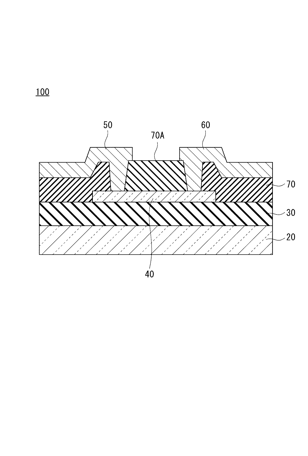
表1に示すように、実施例1から実施例4は、式(5)から式(8)を満たす原子比でGa、Sn、Inおよびレアアース元素Xを含んでおり、成膜後は、エロージョンの形成以外、外観に大きな変化がなかった。相対密度は95%以上であり、バルク抵抗は30mΩ・cm以下であった。
表2に示すように、比較例1はレアアース元素Xを含んでおらず、成膜後のエロージョン部に黒色異物およびヘアーラインクラックが発生した。
比較例2は、Gaの含有量が式(5)の上限外れであり、成膜後のエロージョン部に黒色異物およびヘアーラインクラックが発生した。
比較例3は、Inの含有量が式(7)の下限外れであり、焼結時に試料が割れてしまい、ターゲットを製造できなかった。
比較例4は、Gaの含有量が式(5)の上限外れ、Inの含有量が式(7)の下限外れであり、成膜後のエロージョン部に黒色異物およびヘアーラインクラックが発生した。As shown in Table 1, Examples 1 to 4 contain Ga, Sn, In and a rare earth element X in an atomic ratio satisfying the formulas (5) to (8), and after film formation, erosion There was no significant change in appearance other than the formation of. The relative density was 95% or more, and the bulk resistance was 30 mΩ · cm or less.
As shown in Table 2, Comparative Example 1 did not contain the rare earth element X, and black foreign matter and hairline cracks were generated in the erosion portion after the film formation.
In Comparative Example 2, the Ga content was out of the upper limit of the formula (5), and black foreign matter and hairline cracks were generated in the erosion portion after the film formation.
In Comparative Example 3, the In content was out of the lower limit of the formula (7), the sample cracked during sintering, and the target could not be produced.
In Comparative Example 4, the Ga content was out of the upper limit of the formula (5), the In content was out of the lower limit of the formula (7), and black foreign matter and hairline cracks were generated in the erosion portion after the film formation.
[薄膜トランジスタの製造及び性能評価]
実施例A
(1)成膜工程
実施例1で製造した酸化物焼結体から作製したスパッタリングターゲットを用いて、表2に示す成膜条件で、熱酸化膜(ゲート絶縁膜)付きのシリコンウエハ(ゲート電極)上に、メタルマスクを介して50nmの薄膜(酸化物半導体層)を形成した。スパッタガスとして、高純度アルゴン及び高純度酸素1%の混合ガスを用い、スパッタリングを行った。
薄膜(酸化物半導体層)の成膜は4インチφターゲットを用いて、200kHz、デューディー比50%、出力200Wにて行った。得られた半導体膜の下記特性を評価した。結果を表3に示す。[Manufacturing and performance evaluation of thin film transistors]
Example A
(1) Film formation process Using a sputtering target prepared from the oxide sintered body manufactured in Example 1, a silicon wafer (gate electrode) with a thermal oxide film (gate insulating film) was used under the film formation conditions shown in Table 2. ), A thin film (oxide semiconductor layer) of 50 nm was formed through a metal mask. Sputtering was performed using a mixed gas of high-purity argon and high-purity oxygen of 1% as the sputtering gas.
The thin film (oxide semiconductor layer) was formed using a 4-inch φ target at 200 kHz, a due diligence ratio of 50%, and an output of 200 W. The following characteristics of the obtained semiconductor film were evaluated. The results are shown in Table 3.
(2)ソース・ドレイン電極の形成
メタルマスクを用いてソース・ドレイン電極として、チタン金属をスパッタ成膜で付けた後、得られた積層体を大気中にて350℃、30分間加熱処理した。薄膜トランジスタ(TFT)を完成し、TFTの特性を評価した。(2) Formation of Source / Drain Electrode A titanium metal was attached as a source / drain electrode using a metal mask by sputter film formation, and then the obtained laminate was heat-treated in the air at 350 ° C. for 30 minutes. A thin film transistor (TFT) was completed and the characteristics of the TFT were evaluated.
<TFTの特性評価>
得られたTFTの下記特性について、以下の項目の評価を行った。<Evaluation of TFT characteristics>
The following items were evaluated for the following characteristics of the obtained TFT.
飽和移動度は、ドレイン電圧に5V印加した場合の伝達特性から求めた。具体的に、伝達特性Id−Vgのグラフを作成し、各Vgのトランスコンダクタンス(Gm)を算出し、線形領域の式により飽和移動度を導いた。尚、Gmは∂(Id)/∂(Vg)によって表され、Vgは−15〜25Vまで印加し、その範囲での最大移動度を飽和移動度と定義した。本明細書において特に断らない限り、飽和移動度はこの方法で評価した。上記Idはソース・ドレイン電極間の電流、Vgはソース・ドレイン電極間に電圧Vdを印加したときのゲート電圧である。 The saturation mobility was determined from the transfer characteristics when 5 V was applied to the drain voltage. Specifically, a graph of the transfer characteristic Id-Vg was created, the transconductance (Gm) of each Vg was calculated, and the saturation mobility was derived from the equation in the linear region. Gm is represented by ∂ (Id) / ∂ (Vg), Vg is applied from -15 to 25V, and the maximum mobility in that range is defined as saturation mobility. Unless otherwise stated herein, saturation mobility was assessed in this way. The above Id is the current between the source and drain electrodes, and Vg is the gate voltage when the voltage Vd is applied between the source and drain electrodes.
閾値電圧(Vth)は、伝達特性のグラフよりId=10−9AでのVgと定義した。The threshold voltage (Vth) was defined as Vg at Id = 10-9 A from the graph of transmission characteristics.
on−off比は、Vg=−10VのIdの値をオフ電流値とし、Vg=20VのIdの値をオン電流値として比[On/Off]を決めた。
結果を表3の「加熱処理後のTFTの特性」に示す。As for the on-off ratio, the ratio [On / Off] was determined by using the value of Id of Vg = -10V as the off-current value and the value of Id of Vg = 20V as the on-current value.
The results are shown in "Characteristics of TFT after heat treatment" in Table 3.
(3)保護絶縁膜の形成
加熱処理後の半導体膜の上に、基板温度300℃で化学蒸着法(CVD)により、SiO2膜(保護絶縁膜;層間絶縁膜)を形成し、その後、後アニールとして350℃、1時間加熱処理を行った。
SiO2膜成膜後の加熱処理を行ったTFTの特性を「加熱処理後のTFTの特性」と同じ条件で評価した。結果を表3の「CVDでSiO2膜成膜後、加熱処理して得られたTFTの特性」に示す。 (3) Formation of protective insulating film A SiO 2 film (protective insulating film; interlayer insulating film) is formed on the heat-treated semiconductor film by a chemical vapor deposition method (CVD) at a substrate temperature of 300 ° C., and then later. As annealing, heat treatment was performed at 350 ° C. for 1 hour.
The characteristics of the TFT that had been heat-treated after the SiO 2 film was formed were evaluated under the same conditions as the "characteristics of the TFT after the heat treatment". The results are shown in Table 3 "Characteristics of TFT obtained by heat-treating after forming a SiO 2 film by CVD".
<半導体膜の特性評価>
また、酸化物薄膜のみをガラス基板に載せたサンプルも同時に作製し、以下の手順で、半導体膜成膜の加熱処理後、並びにCVDでのSiO2膜成膜直後及び加熱処理後の各段階でホール測定を行い、キャリヤー密度の増減等の半導体膜の特性を測定、評価した。
尚、得られた酸化物薄膜は、用いたターゲットと同じ原子比組成を有していた。<Characteristic evaluation of semiconductor film>
In addition, a sample in which only the oxide thin film is placed on a glass substrate is also prepared at the same time, and the following procedure is performed at each stage after the heat treatment for semiconductor film formation, immediately after the SiO 2 film formation by CVD, and after the heat treatment. Hole measurement was performed to measure and evaluate the characteristics of the semiconductor film such as increase / decrease in carrier density.
The obtained oxide thin film had the same atomic ratio composition as the target used.
ホール効果測定:
TFT製造工程と同様に図27に示すように、ガラス基板上に厚さ50nmの酸化物半導体膜を成膜し、加熱処理を行った後、1cm角の正方形に切り出して、4角に金(Au)を2mm×2mm以下の大きさ位になるようにメタルマスクを用いてイオンコーターで成膜し、Au金属上にインジウムはんだを乗せて接触を良くしてホール効果測定用サンプルとした。
ガラス基板には、日本電気硝子株式会社製ABC−Gを用いた。
ホール効果測定用サンプルをホール効果・比抵抗測定装置(ResiTest8300型、東陽テクニカ社製)にセットし、室温においてホール効果を評価し、キャリヤー密度及び移動度を求めた。結果を表3の「加熱処理後の半導体膜の特性」に示す。Hall effect measurement:
As shown in FIG. 27, as in the TFT manufacturing process, an oxide semiconductor film having a thickness of 50 nm is formed on a glass substrate, heat-treated, and then cut into a 1 cm square and gold (square). Au) was formed into a film with an ion coater using a metal mask so as to have a size of 2 mm × 2 mm or less, and indium solder was placed on the Au metal to improve contact and used as a sample for Hall effect measurement.
ABC-G manufactured by Nippon Electric Glass Co., Ltd. was used as the glass substrate.
A sample for Hall effect measurement was set in a Hall effect / resistivity measuring device (ResiTest 8300 type, manufactured by Toyo Technica Co., Ltd.), and the Hall effect was evaluated at room temperature to determine the carrier density and mobility. The results are shown in "Characteristics of semiconductor film after heat treatment" in Table 3.
上記ホール効果測定用サンプルの半導体膜上に、図28に示すように、CVD装置によりSiO2膜を成膜したのち、「加熱処理後の半導体膜の特性」と同じ条件でホール測定を実施した。結果を表3の「CVDでSiO2膜成膜後の半導体膜の特性」に示す。
さらに加熱処理後にも「加熱処理後の半導体膜の特性」と同じ条件でホール測定を行った。SiO2膜に測定用針をAu金属の層まで突き刺し、コンタクトを取った。結果を表3の「CVDでSiO2膜成膜後、加熱処理した半導体膜の特性」に示す。 As shown in FIG. 28, a SiO 2 film was formed on the semiconductor film of the sample for Hall effect measurement by a CVD apparatus, and then Hall measurement was performed under the same conditions as “characteristics of the semiconductor film after heat treatment”. .. The results are shown in Table 3 “Characteristics of semiconductor film after film formation of SiO 2 film by CVD”.
Further, even after the heat treatment, the hole measurement was performed under the same conditions as the "characteristics of the semiconductor film after the heat treatment". A measuring needle was pierced into the SiO 2 film up to the Au metal layer to make contact. The results are shown in Table 3 "Characteristics of semiconductor film heat-treated after forming a SiO 2 film by CVD".
半導体膜の結晶特性:
スパッタ後(膜堆積後)の加熱していない膜、及び加熱した後の膜の結晶性を、X線回折(XRD)測定によって評価した結果を表3に示した。Crystal characteristics of semiconductor film:
Table 3 shows the results of evaluating the crystallinity of the unheated film after sputtering (after film deposition) and the film after heating by X-ray diffraction (XRD) measurement.
半導体膜のバンドギャップ:
石英基板上に成膜し、半導体膜と同様に熱処理した薄膜資料の透過スペクトルを測定し、横軸の波長をエネルギー(eV)に、縦軸の透過率を
(αhν)1/2
(ここで、
α:吸収係数
h:プランク定数
ν:振動数
である。)
に変換したあと、吸収が立ち上がる部分に直線をフィッティングし、その直線がベースラインと交わるところのeV値を算出した。Semiconductor film bandgap:
The transmission spectrum of a thin film material formed on a quartz substrate and heat-treated in the same manner as a semiconductor film is measured, and the wavelength on the horizontal axis is energy (eV) and the transmittance on the vertical axis is (αhν) 1/2.
(here,
α: Absorption coefficient h: Planck constant ν: Frequency. )
After conversion to, a straight line was fitted to the portion where absorption rises, and the eV value at the intersection of the straight line with the baseline was calculated.
実施例B及び比較例A:
表3に示した実施例で製造した酸化物焼結体から作製したスパッタリングターゲットを用い、表3に示した条件とした以外は、実施例Aと同様にして半導体膜および薄膜トランジスタを製造し、評価した。結果を表3に示す。Example B and Comparative Example A:
Using a sputtering target prepared from the oxide sintered body produced in the examples shown in Table 3, a semiconductor film and a thin film transistor were produced and evaluated in the same manner as in Example A except that the conditions shown in Table 3 were met. did. The results are shown in Table 3.
表3に示すように、実施例A、実施例Bは、実施例1、実施例2の焼結体を用いて半導体膜を成膜したものであり、加熱後でもTFTとしての特性が得られていた。
比較例Aは、比較例1の焼結体を用いて半導体膜を製膜したものであり、加熱すると膜が導通してしまい、TFTとしての特性が得られなかった。As shown in Table 3, in Examples A and B, a semiconductor film was formed by using the sintered bodies of Examples 1 and 2, and the characteristics as a TFT can be obtained even after heating. Was there.
In Comparative Example A, a semiconductor film was formed by using the sintered body of Comparative Example 1, and when heated, the film became conductive and the characteristics as a TFT could not be obtained.
本発明の一態様の酸化物半導体膜は、薄膜トランジスタ等の半導体膜として有用である。
本発明の一態様の酸化物焼結体は、スパッタリングターゲット材として有用である。The oxide semiconductor film of one aspect of the present invention is useful as a semiconductor film for thin film transistors and the like.
The oxide sintered body of one aspect of the present invention is useful as a sputtering target material.
1 :酸化物焼結体
3 :バッキングプレート
20 :シリコンウエハ
30 :ゲート絶縁膜
40 :酸化物半導体薄膜
50 :ソース電極
60 :ドレイン電極
70 :層間絶縁膜
70A :層間絶縁膜
70B :層間絶縁膜
100 :薄膜トランジスタ
100A :薄膜トランジスタ
300 :基板
301 :画素部
302 :第1の走査線駆動回路
303 :第2の走査線駆動回路
304 :信号線駆動回路
310 :容量配線
312 :ゲート配線
313 :ゲート配線
314 :ドレイン電極
316 :トランジスタ
317 :トランジスタ
318 :第1の液晶素子
319 :第2の液晶素子
320 :画素部
321 :スイッチング用トランジスタ
322 :駆動用トランジスタ
3002 :フォトダイオード
3004 :転送トランジスタ
3006 :リセットトランジスタ
3008 :増幅トランジスタ
3010 :信号電荷蓄積部
3100 :電源線
3110 :リセット電源線
3120 :垂直出力線
1: Oxide sintered body 3: Backing plate 20: Silicon wafer 30: Gate insulating film 40: Oxide semiconductor thin film 50: Source electrode 60: Drain electrode 70:
Claims (12)
0.01≦Ga/(In+Ga+Sn)≦0.30 ・・・(1)
0.01≦Sn/(In+Ga+Sn)≦0.40 ・・・(2)
0.55≦In/(In+Ga+Sn)≦0.98 ・・・(3)
で含有し、
かつ、レアアース元素Xを下記原子比
0.03≦X/(In+Ga+Sn+X)≦0.25 ・・・(4)
で含有する酸化物半導体膜。 In, Ga and Sn have the following atomic ratios 0.01 ≤ Ga / (In + Ga + Sn) ≤ 0.30 ... (1)
0.01 ≤ Sn / (In + Ga + Sn) ≤ 0.40 ... (2)
0.55 ≤ In / (In + Ga + Sn) ≤ 0.98 ... (3)
Contained in
And the rare earth element X has the following atomic ratio 0.03 ≤ X / (In + Ga + Sn + X) ≤ 0.25 ... (4)
Oxide semiconductor film contained in.
0.01≦Ga/(In+Ga+Sn)≦0.30 ・・・(5)
0.01≦Sn/(In+Ga+Sn)≦0.40 ・・・(6)
0.55≦In/(In+Ga+Sn)≦0.98 ・・・(7)
で含有し、
かつ、レアアース元素Xを下記原子比
0.03≦X/(In+Ga+Sn+X)≦0.25 ・・・(8)
で含有するスパッタリングターゲット用酸化物焼結体。 In, Ga and Sn have the following atomic ratios 0.01 ≤ Ga / (In + Ga + Sn) ≤ 0.30 ... (5)
0.01 ≤ Sn / (In + Ga + Sn) ≤ 0.40 ... (6)
0.55 ≤ In / (In + Ga + Sn) ≤ 0.98 ... (7)
Contained in
And the rare earth element X has the following atomic ratio 0.03 ≤ X / (In + Ga + Sn + X) ≤ 0.25 ... (8)
Oxide sintered body for sputtering target contained in.
Applications Claiming Priority (3)
| Application Number | Priority Date | Filing Date | Title |
|---|---|---|---|
| JP2017031460 | 2017-02-22 | ||
| JP2017031460 | 2017-02-22 | ||
| PCT/JP2018/005245 WO2018155301A1 (en) | 2017-02-22 | 2018-02-15 | Oxide semiconductor film, thin film transistor, oxide sintered body and sputtering target |
Publications (2)
| Publication Number | Publication Date |
|---|---|
| JPWO2018155301A1 JPWO2018155301A1 (en) | 2019-12-12 |
| JP6902090B2 true JP6902090B2 (en) | 2021-07-14 |
Family
ID=63253791
Family Applications (1)
| Application Number | Title | Priority Date | Filing Date |
|---|---|---|---|
| JP2019501265A Active JP6902090B2 (en) | 2017-02-22 | 2018-02-15 | Oxide semiconductor film, thin film transistor, oxide sintered body for sputtering target, sputtering target and electronic equipment |
Country Status (6)
| Country | Link |
|---|---|
| US (1) | US11251310B2 (en) |
| JP (1) | JP6902090B2 (en) |
| KR (1) | KR102380806B1 (en) |
| CN (1) | CN110447093B (en) |
| TW (1) | TWI786088B (en) |
| WO (1) | WO2018155301A1 (en) |
Families Citing this family (17)
| Publication number | Priority date | Publication date | Assignee | Title |
|---|---|---|---|---|
| CN112289863B (en) * | 2020-09-25 | 2024-07-19 | 华南理工大学 | Metal oxide semiconductor and thin film transistor and their applications |
| KR102598375B1 (en) * | 2018-08-01 | 2023-11-06 | 이데미쓰 고산 가부시키가이샤 | Crystal structure compound, oxide sintered body, sputtering target, crystalline oxide thin film, amorphous oxide thin film, thin film transistor and electronic equipment |
| CN110797395A (en) * | 2019-09-18 | 2020-02-14 | 华南理工大学 | Doped metal oxide semiconductors and thin film transistors and their applications |
| CN110767745A (en) * | 2019-09-18 | 2020-02-07 | 华南理工大学 | Composite metal oxide semiconductor, thin film transistor and application |
| JP7373428B2 (en) * | 2020-02-14 | 2023-11-02 | 株式会社神戸製鋼所 | Thin film transistors, oxide semiconductor thin films, and sputtering targets |
| US12696492B2 (en) * | 2020-04-24 | 2026-07-28 | ORCA Computing Limited | Solid-state device with optical waveguide as floating gate electrode |
| US12690233B2 (en) | 2020-05-29 | 2026-07-21 | Taiwan Semiconductor Manufacturing Company Limited | Raised source/drain oxide semiconducting thin film transistor and methods of making the same |
| DE102021108615A1 (en) * | 2020-05-29 | 2021-12-02 | Taiwan Semiconductor Manufacturing Company, Ltd. | INCREASED SOURCE / DRAIN OXIDE SEMICONDUCTOR THIN FILM TRANSISTOR AND METHOD OF MANUFACTURING THEREOF |
| CN112390622A (en) * | 2020-11-23 | 2021-02-23 | 先导薄膜材料(广东)有限公司 | Preparation method of EIGZO target material |
| KR20220090871A (en) * | 2020-12-23 | 2022-06-30 | 한양대학교 산학협력단 | High mobility transistor device using crystallization of igto oxide semiconductor and manufacturing method thereof |
| US12604537B2 (en) * | 2020-12-23 | 2026-04-14 | Iucf-Hyu (Industry-University Cooperation Foundation Hanyang University) | High mobility transistor element resulting from IGTO oxide semiconductor crystallization, and production method for same |
| KR20220094735A (en) * | 2020-12-29 | 2022-07-06 | 에이디알씨 주식회사 | Crystallized oxide semiconductor thin film and method of forming the same and thin film transistor and method of manufacturing the same and display panel and electronic device |
| KR102888127B1 (en) * | 2021-05-18 | 2025-11-20 | 삼성전자주식회사 | Semiconductor memory device and method for manufacturing the same |
| US12598794B2 (en) * | 2022-02-17 | 2026-04-07 | Boe Technology Group Co., Ltd. | Semiconductor material, light-emitting device, display panel and display device |
| CN116334557B (en) * | 2023-03-30 | 2025-02-25 | 浙江大学 | A fluorine-erbium co-doped tin oxide film and its preparation method and application |
| CN116813310B (en) * | 2023-06-01 | 2024-06-07 | 先导薄膜材料(广东)有限公司 | Rare earth element doped indium tin gallium oxide target material and preparation method thereof |
| WO2026157788A1 (en) * | 2025-01-24 | 2026-07-30 | 广州华星光电半导体显示技术有限公司 | Thin film transistor, display panel and display device |
Family Cites Families (22)
| Publication number | Priority date | Publication date | Assignee | Title |
|---|---|---|---|---|
| JPH04272612A (en) | 1991-02-26 | 1992-09-29 | Kojundo Chem Lab Co Ltd | Transparent electrode |
| US20020017331A1 (en) | 2000-06-30 | 2002-02-14 | Renaud Michel C. | Variable stiffness bellows |
| US20040180217A1 (en) | 2001-08-02 | 2004-09-16 | Kazuyoshi Inoue | Sputtering target, transparent conductive film, and their manufacturing method |
| ITMI20012075A1 (en) * | 2001-10-08 | 2003-04-08 | Consiglio Nazionale Ricerche | PROCEDURE FOR THE CONFERENCE AND CONTROL ON MICRO AND NANOMATRIC STAIRS OF THE STRUCTURAL ELECTRIC PROPERTY AND ANISOTROPY PROPERTIES AND |
| KR100514952B1 (en) * | 2003-01-15 | 2005-09-14 | 주식회사 피앤아이 | Method of forming indium tin oxide thin film including a seed layer and a bulk layer utilizing an optimized sequential sputter deposition |
| JP4985928B2 (en) * | 2005-10-21 | 2012-07-25 | 信越化学工業株式会社 | Multi-layer coated corrosion resistant member |
| DE102007009546B4 (en) | 2007-02-27 | 2008-12-04 | Continental Automotive Gmbh | Method and device for controlling an internal combustion engine of a motor vehicle which can be switched to operation with CNG gas |
| WO2009128424A1 (en) | 2008-04-16 | 2009-10-22 | 住友金属鉱山株式会社 | Thin film transistor type substrate, thin film transistor type liquid crystal display device and method for manufacturing thin film transistor type substrate |
| WO2009145272A1 (en) * | 2008-05-28 | 2009-12-03 | 三菱マテリアル株式会社 | Composition for ferroelectric thin film formation, method for ferroelectric thin film formation, and ferroelectric thin film formed by the method |
| JP2010030824A (en) * | 2008-07-28 | 2010-02-12 | Idemitsu Kosan Co Ltd | Metal phase-containing indium oxide sintered compact and method for producing the same |
| KR101533391B1 (en) * | 2008-08-06 | 2015-07-02 | 삼성디스플레이 주식회사 | Thin film transistor substrate and manufacturing method thereof |
| KR20110047308A (en) | 2009-10-30 | 2011-05-09 | 삼성코닝정밀소재 주식회사 | Indium tin oxide sputtering target and transparent conductive film prepared using the same |
| JP2011174134A (en) | 2010-02-24 | 2011-09-08 | Idemitsu Kosan Co Ltd | In-Ga-Sn-based oxide sintered body, target, oxide semiconductor film, and semiconductor element |
| US9224820B2 (en) | 2012-05-31 | 2015-12-29 | Samsung Corning Advanced Glass, Llc | Oxide semiconductor sputtering target, method of manufacturing thin-film transistors using the same, and thin film transistor manufactured using the same |
| JP2014111818A (en) | 2012-11-09 | 2014-06-19 | Idemitsu Kosan Co Ltd | Sputtering target, oxide semiconductor thin film, and production method of them |
| JP6064895B2 (en) * | 2013-12-27 | 2017-01-25 | 住友金属鉱山株式会社 | Indium oxide-based oxide sintered body and method for producing the same |
| WO2015108110A1 (en) | 2014-01-15 | 2015-07-23 | 株式会社神戸製鋼所 | Thin-film transistor |
| WO2015115330A1 (en) * | 2014-01-31 | 2015-08-06 | 独立行政法人物質・材料研究機構 | Thin-film transistor, oxide semiconductor, and method for producing same |
| KR101563700B1 (en) | 2014-03-17 | 2015-10-27 | 삼성중공업 주식회사 | Painting Device |
| KR102514007B1 (en) | 2015-04-22 | 2023-03-27 | 가부시키가이샤 한도오따이 에네루기 켄큐쇼 | Image capture device, method for driving image capture device, and electronic device |
| JP6610062B2 (en) * | 2015-07-31 | 2019-11-27 | 日本製鉄株式会社 | Titanium plate |
| JP6141381B2 (en) | 2015-10-14 | 2017-06-07 | 出光興産株式会社 | Manufacturing method of sputtering target |
-
2018
- 2018-02-15 JP JP2019501265A patent/JP6902090B2/en active Active
- 2018-02-15 KR KR1020197023688A patent/KR102380806B1/en active Active
- 2018-02-15 US US16/485,381 patent/US11251310B2/en active Active
- 2018-02-15 WO PCT/JP2018/005245 patent/WO2018155301A1/en not_active Ceased
- 2018-02-15 CN CN201880012548.4A patent/CN110447093B/en active Active
- 2018-02-22 TW TW107105954A patent/TWI786088B/en active
Also Published As
| Publication number | Publication date |
|---|---|
| US11251310B2 (en) | 2022-02-15 |
| TW201833062A (en) | 2018-09-16 |
| WO2018155301A1 (en) | 2018-08-30 |
| KR102380806B1 (en) | 2022-03-30 |
| CN110447093A (en) | 2019-11-12 |
| US20190378933A1 (en) | 2019-12-12 |
| JPWO2018155301A1 (en) | 2019-12-12 |
| KR20190117528A (en) | 2019-10-16 |
| CN110447093B (en) | 2023-04-25 |
| TWI786088B (en) | 2022-12-11 |
Similar Documents
| Publication | Publication Date | Title |
|---|---|---|
| TWI786088B (en) | Oxide semiconductor film, thin film transistor, oxide sintered body for sputtering target, sputtering target, display device, and solid-state imaging device | |
| JP7075934B2 (en) | Sputtering targets, oxide semiconductor thin films, thin film transistors and electrical equipment | |
| JP6834062B2 (en) | Crystal structure compounds, oxide sintered bodies, and sputtering targets | |
| JP7092746B2 (en) | Oxide sintered body, sputtering target, oxide semiconductor thin film, thin film transistor, and electronic device | |
| JP7082947B2 (en) | Manufacturing method of amorphous oxide semiconductor film, oxide sintered body, thin film transistor, sputtering target, electronic device and amorphous oxide semiconductor film | |
| JP6869157B2 (en) | Oxide sintered body, sputtering target, amorphous oxide semiconductor thin film, and thin film transistor | |
| JP6956748B2 (en) | Oxide semiconductor film, thin film transistor, oxide sintered body and sputtering target | |
| TW201536937A (en) | Oxide sintered body, target for sputtering, and oxide semiconductor film obtained using the same | |
| KR20250165360A (en) | Oxide sintered body, sputtering target, oxide thin film, thin film transistor, and electronic device |
Legal Events
| Date | Code | Title | Description |
|---|---|---|---|
| A621 | Written request for application examination |
Free format text: JAPANESE INTERMEDIATE CODE: A621 Effective date: 20200903 |
|
| A131 | Notification of reasons for refusal |
Free format text: JAPANESE INTERMEDIATE CODE: A131 Effective date: 20210511 |
|
| A521 | Request for written amendment filed |
Free format text: JAPANESE INTERMEDIATE CODE: A523 Effective date: 20210602 |
|
| TRDD | Decision of grant or rejection written | ||
| A01 | Written decision to grant a patent or to grant a registration (utility model) |
Free format text: JAPANESE INTERMEDIATE CODE: A01 Effective date: 20210615 |
|
| A61 | First payment of annual fees (during grant procedure) |
Free format text: JAPANESE INTERMEDIATE CODE: A61 Effective date: 20210618 |
|
| R150 | Certificate of patent or registration of utility model |
Ref document number: 6902090 Country of ref document: JP Free format text: JAPANESE INTERMEDIATE CODE: R150 |