JP6884149B2 - Software-defined FIFO buffer for multithreaded access - Google Patents
Software-defined FIFO buffer for multithreaded access Download PDFInfo
- Publication number
- JP6884149B2 JP6884149B2 JP2018529209A JP2018529209A JP6884149B2 JP 6884149 B2 JP6884149 B2 JP 6884149B2 JP 2018529209 A JP2018529209 A JP 2018529209A JP 2018529209 A JP2018529209 A JP 2018529209A JP 6884149 B2 JP6884149 B2 JP 6884149B2
- Authority
- JP
- Japan
- Prior art keywords
- request
- buffer controller
- buffer
- write
- processing device
- Prior art date
- Legal status (The legal status is an assumption and is not a legal conclusion. Google has not performed a legal analysis and makes no representation as to the accuracy of the status listed.)
- Active
Links
Images


Classifications
-
- G—PHYSICS
- G06—COMPUTING; CALCULATING OR COUNTING
- G06F—ELECTRIC DIGITAL DATA PROCESSING
- G06F3/00—Input arrangements for transferring data to be processed into a form capable of being handled by the computer; Output arrangements for transferring data from processing unit to output unit, e.g. interface arrangements
- G06F3/06—Digital input from, or digital output to, record carriers, e.g. RAID, emulated record carriers or networked record carriers
- G06F3/0601—Interfaces specially adapted for storage systems
- G06F3/0628—Interfaces specially adapted for storage systems making use of a particular technique
- G06F3/0655—Vertical data movement, i.e. input-output transfer; data movement between one or more hosts and one or more storage devices
- G06F3/0659—Command handling arrangements, e.g. command buffers, queues, command scheduling
-
- G—PHYSICS
- G06—COMPUTING; CALCULATING OR COUNTING
- G06F—ELECTRIC DIGITAL DATA PROCESSING
- G06F5/00—Methods or arrangements for data conversion without changing the order or content of the data handled
- G06F5/06—Methods or arrangements for data conversion without changing the order or content of the data handled for changing the speed of data flow, i.e. speed regularising or timing, e.g. delay lines, FIFO buffers; over- or underrun control therefor
- G06F5/10—Methods or arrangements for data conversion without changing the order or content of the data handled for changing the speed of data flow, i.e. speed regularising or timing, e.g. delay lines, FIFO buffers; over- or underrun control therefor having a sequence of storage locations each being individually accessible for both enqueue and dequeue operations, e.g. using random access memory
- G06F5/12—Means for monitoring the fill level; Means for resolving contention, i.e. conflicts between simultaneous enqueue and dequeue operations
-
- G—PHYSICS
- G06—COMPUTING; CALCULATING OR COUNTING
- G06F—ELECTRIC DIGITAL DATA PROCESSING
- G06F3/00—Input arrangements for transferring data to be processed into a form capable of being handled by the computer; Output arrangements for transferring data from processing unit to output unit, e.g. interface arrangements
- G06F3/06—Digital input from, or digital output to, record carriers, e.g. RAID, emulated record carriers or networked record carriers
- G06F3/0601—Interfaces specially adapted for storage systems
- G06F3/0602—Interfaces specially adapted for storage systems specifically adapted to achieve a particular effect
- G06F3/0604—Improving or facilitating administration, e.g. storage management
-
- G—PHYSICS
- G06—COMPUTING; CALCULATING OR COUNTING
- G06F—ELECTRIC DIGITAL DATA PROCESSING
- G06F3/00—Input arrangements for transferring data to be processed into a form capable of being handled by the computer; Output arrangements for transferring data from processing unit to output unit, e.g. interface arrangements
- G06F3/06—Digital input from, or digital output to, record carriers, e.g. RAID, emulated record carriers or networked record carriers
- G06F3/0601—Interfaces specially adapted for storage systems
- G06F3/0668—Interfaces specially adapted for storage systems adopting a particular infrastructure
- G06F3/0671—In-line storage system
- G06F3/0673—Single storage device
Description
本発明は、FIFOバッファを実施するためのシステム及び方法に関する。 The present invention relates to systems and methods for implementing FIFO buffers.
従来のコンピュータシステムでは、先入れ先出し(FIFO)バッファは複数のスレッドによってアクセスされる場合がある。しかしながら、従来のシステムでは、同時に1つのスレッドのみがFIFOバッファにアクセスすることができる。このことにより、遅延と処理オーバヘッドとがもたらされるが、これは、FIFOバッファのデータ構造が別のスレッドにより解放されることを待ちながら、スレッドをブロックすることによって同時アクセスを阻止するためである。 In traditional computer systems, the first-in first-out (FIFO) buffer may be accessed by multiple threads. However, in traditional systems, only one thread can access the FIFO buffer at a time. This introduces delays and processing overhead in order to prevent simultaneous access by blocking threads while waiting for the data structures in the FIFO buffer to be released by another thread.
本明細書に開示されるシステム及び方法は、複数のスレッドにより同時にアクセス可能なFIFOバッファを実施するための改善したアプローチを提供する。 The systems and methods disclosed herein provide an improved approach for implementing FIFO buffers that are simultaneously accessible by multiple threads.
発明の利点が容易に理解されるように、簡単に上述した発明のより具体的な説明は、添付の図面で説明された特定の実施形態を参照することによって提供されることになる。これらの図面は、発明の典型的な実施形態のみを示し、それ故、その範囲を限定するとみされないと理解され、発明は、添付の図面の使用を通じて更なる特異性と詳細が記述及び説明される。
本明細書内で包括的に記述及びの図示されるような本発明の構成要素は、幅広い様々な異なる構成で配置及び設計され得ることが容易に理解されるであろう。したがって、図面で表されるような以下の発明の実施形態のより詳細な説明は、請求項で示されるような発明の範囲を限定することを意図せず、本発明に従って現在企図される実施形態の特定の例を代表するにすぎない。現在記述された実施形態は、全体を通じて同様の部分が同様の数字で示されている図面を参照することによって最も正確に理解されるであろう。 It will be readily appreciated that the components of the invention as comprehensively described and illustrated herein can be arranged and designed in a wide variety of different configurations. Therefore, a more detailed description of the following embodiments of the invention, as shown in the drawings, is not intended to limit the scope of the invention as set forth in the claims, and is currently contemplated in accordance with the present invention. It only represents a specific example of. The embodiments currently described will be most accurately understood by reference to drawings in which similar parts are shown with similar numbers throughout.
本発明に従った実施形態は、装置、方法、又はコンピュータプログラム製品として具体化されてもよい。したがって、本発明は、完全にハードウェアの実施形態、(ファームウェア、常駐ソフトウェア、マイクロコード等を含む)完全にソフトウェアの実施形態、又は“モジュール”若しくは“システム”として本明細書で概して全て称され得るソフトウェア及びハードウェアの態様の組み合わせの実施形態をとってもよい。更に、本発明は、任意の有形的表現媒体内で具体化されるコンピュータプログラム製品の形式をとってもよく、こうした有形的表現媒体内で、コンピュータ使用可能なプログラムコードが具体化される。 Embodiments according to the present invention may be embodied as devices, methods, or computer program products. Accordingly, the present invention is generally referred to herein as a fully hardware embodiment, a fully software embodiment (including firmware, resident software, microcode, etc.), or a "module" or "system". An embodiment of a combination of aspects of the software and hardware obtained may be taken. Further, the present invention may take the form of a computer program product embodied in any tangible expression medium, in which computer-usable program code is embodied.
非一時的媒体を含めた、1つ以上のコンピュータ使用可能な又はコンピュータ可読な媒体の組み合わせが利用されてもよい。例えば、コンピュータ可読媒体は、携帯可能なコンピュータディスケット、ハードディスク、ランダムアクセスメモリ(RAM)デバイス、リードオンリーメモリ(ROM)デバイス、消去可能プログラム可能リードオンリーメモリ(EPROM又はフラッシュメモリ)デバイス、携帯可能なコンパクトディスクリードオンリーメモリ(CDROM)、光学記憶デバイス、及び磁気記憶デバイスの内の1つ以上を含んでもよい。選択された実施形態では、コンピュータ可読媒体は、命令実行システム、装置(apparatus)、又はデバイス(device)によってされる、又はそれに関連して使用するためのプログラムを含み得、格納し得、通信し得、伝搬し得、又は搬送し得る任意の非一時的媒体を含んでもよい。 A combination of one or more computer-enabled or computer-readable media, including non-temporary media, may be utilized. For example, computer-readable media include portable computer diskettes, hard disks, random access memory (RAM) devices, read-only memory (ROM) devices, erasable programmable read-only memory (EPROM or flash memory) devices, and portable compacts. It may include one or more of a disk read-only memory (CDROM), an optical storage device, and a magnetic storage device. In selected embodiments, the computer-readable medium may include, store, and communicate programs for use by or in connection with an instruction execution system, apparatus, or device. It may include any non-transient medium that can be obtained, propagated, or transported.
本発明の動作を遂行するためのコンピュータプログラムコードは、Java、スモールトーク、又はC++等のオブジェクト指向プログラミング言語、及び、“C”プログラミング言語若しくは同様のプログラミング言語等の同様の従来の手続型プログラミング言語を含む1つ以上のプログラミング言語の任意の組み合わせで書き込まれてもよい。プログラムコードは、スタンドアローンなソフトウェアパッケージとしてのコンピュータシステム上で全体的に実行されること、スタンドアローンなハードウェアユニット上で実行されること、コンピュータから幾らか間隔が空けられたリモートコンピュータ上で部分的にされること、又はリモートコンピュータ若しくはサーバ上で全体的に実行されることもある。後者の場合では、リモートコンピュータは、ローカルエリアネットワーク(LAN)又は広域ネットワーク(WAN)を含む任意の種類のネットワークを通じてコンピュータに接続されてもよく、又は該接続は(例えば、インターネットサービスプロバイダを用いてインターネットを通じて)外部のコンピュータへなされてもよい。 The computer program code for performing the operations of the present invention is an object-oriented programming language such as Java, SmallTalk, or C ++, and a similar conventional procedural programming language such as the "C" programming language or a similar programming language. It may be written in any combination of one or more programming languages including. The program code runs entirely on the computer system as a stand-alone software package, runs on a stand-alone hardware unit, and is partly on a remote computer some distance from the computer. It may be targeted or run entirely on a remote computer or server. In the latter case, the remote computer may be connected to the computer through any type of network, including a local area network (LAN) or wide area network (WAN), or the connection may be made (eg, using an internet service provider). It may be done to an external computer (through the internet).
本発明は、本発明の実施形態に従った方法、装置(システム)、及びコンピュータプログラム製品のフローチャートの説明及び/又はブロック図を参照しながら以下に記述される。フローチャートの説明及び/又はブロック図中の各ブロック、並びにフローチャートの説明及び/又はブロック図中のブロックの組み合わせは、コンピュータプログラム命令又はコードによって実施され得ることが理解されるであろう。これらのコンピュータプログラム命令を、機械を生産するための汎用コンピュータ、専用コンピュータ、又はその他のプログラム可能なデータ処理装置のプロセッサに供給することもでき、こうすることで、その命令が、コンピュータ又はその他のプログラム可能なデータ処理装置のプロセッサを介して実行され、フローチャート及び/又はブロック図の1つ以上のブロックで指定される機能/作用を実施するための手段を作り出す。 The present invention is described below with reference to the flow chart description and / or block diagram of methods, devices (systems), and computer program products according to embodiments of the present invention. It will be appreciated that each block in the flowchart description and / or block diagram, and the combination of blocks in the flowchart description and / or block diagram, can be implemented by computer program instructions or code. These computer program instructions can also be fed to the processor of a general purpose computer, dedicated computer, or other programmable data processing device for producing the machine, so that the instructions can be delivered to the computer or other computer. It is executed through the processor of a programmable data processing device and creates means for performing a function / action specified by one or more blocks of a flowchart and / or a block diagram.
これらのコンピュータプログラム命令を、特定の機能を行うようにコンピュータ又はその他のプログラム可能なデータ処理装置に命令を出すことが可能な非一時的コンピュータ可読媒体に格納することもでき、こうすることで、コンピュータ可読媒体に格納された該命令がフローチャート及び/又はブロック図の1つ以上のブロックで指定される機能/作用を実施する命令手段を含む製品を生み出す。 These computer program instructions can also be stored on a non-temporary computer-readable medium capable of issuing instructions to a computer or other programmable data processing device to perform a particular function. The instruction stored in a computer-readable medium produces a product that includes an instruction means that performs a function / action specified by one or more blocks of a flowchart and / or a block diagram.
コンピュータプログラム命令はまたを、コンピュータ又はその他のプログラム可能なデータ処理装置上にロードして、一連の動作ステップをコンピュータ又はその他のプログラム可能装置上で実行させて、コンピュータ実施プロセスであって、コンピュータ又はその他のプログラム可能装置上で実行される命令が、フローチャート及び/又はブロック図の1つ以上のブロックで指定される機能/作用を実施するためのプロセスを提供するようなコンピュータ実施プロセスを生み出してもよい。 A computer program instruction is also a computer implementation process that loads a computer or other programmable data processing device to perform a series of operating steps on the computer or other programmable device, the computer or. Even if instructions executed on other programmable devices spawn computer-implemented processes that provide processes for performing the functions / actions specified in one or more blocks of the flowchart and / or block diagram. Good.
図1は、例示的な計算デバイス100を説明するブロック図である。計算デバイス100は、本明細書で論じられるような様々な手続を実行するために使用されてもよい。計算デバイス100は、サーバ、クライアント、又は任意のその他のコンピューティングエンティティとして機能し得る。計算デバイスは、本明細書で論じられるような様々な監視機能を実行し得、本明細書で論じられるアプリケーションプログラム等、1つ以上のアプリケーションプログラムを実行し得る。計算デバイス100は、デスクトップコンピュータ、ノートブックコンピュータ、サーバコンピュータ、ハンドヘルドコンピュータ、及びタブレットコンピュータ等の任意の幅広い計算デバイスであり得る。
FIG. 1 is a block diagram illustrating an
計算デバイス100は、1つ以上のプロセッサ102、1つ以上のメモリデバイス104、1つ以上のインタフェース106、1つ以上の大容量記憶デバイス108、1つ以上の入出力(I/O)デバイス110、及び表示デバイス130を含み、それら全てがバス112に結合される。(1つ以上の)プロセッサ102は、(1つ以上の)メモリデバイス104及び/又は(1つ以上の)大容量記憶デバイス108に格納された命令を実行する1つ以上のプロセッサ又はコントローラを含む。(1つ以上の)プロセッサ102は、キャッシュメモリ等の様々な種類のコンピュータ可読媒体をも含む。
The
(1つ以上の)メモリデバイス104は、揮発性メモリ(例えば、ランダムアクセスメモリ(RAM)114)及び/又は不揮発性メモリ(例えば、リードオンリーメモリ(ROM)116)等の様々なコンピュータ可読媒体を含む。(1つ以上の)メモリデバイス104は、フラッシュメモリ等の再書き込み可能なROMをも含んでもよい。 The (one or more) memory devices 104 can accommodate various computer-readable media such as volatile memory (eg, random access memory (RAM) 114) and / or non-volatile memory (eg, read-only memory (ROM) 116). Including. The memory device 104 (one or more) may also include a rewritable ROM such as a flash memory.
(1つ以上の)大容量記憶デバイス108は、磁気テープ、磁気ディスク、光ディスク、及び固体状態メモリ(例えば、フラッシュメモリ)等の様々なコンピュータ可読媒体を含む。図1に示すように、特定の大容量記憶デバイスが、ハードディスクドライブ124である。様々なコンピュータ可読媒体からの読み出し及び/又は様々なコンピュータ可読媒体への書き込みができるように、(1つ以上の)大容量記憶デバイス108には様々なドライブも含まれてもよい。(1つ以上の)大容量記憶デバイス108は、取り外し可能媒体126及び/又は不揮発性媒体を含む。 The mass storage device 108 (one or more) includes various computer-readable media such as magnetic tapes, magnetic disks, optical disks, and solid state memory (eg, flash memory). As shown in FIG. 1, the specific mass storage device is the hard disk drive 124. The mass storage device 108 (one or more) may also include various drives so that it can be read from and / or written to various computer-readable media. The mass storage device 108 (one or more) includes a removable medium 126 and / or a non-volatile medium.
(1つ以上の)入出力デバイス110は、データ及び/又はその他の情報が計算デバイス100に入力され得るように、又は計算デバイス100から抽出され得るようにする様々なデバイスを含む。例示的な(1つ以上の)入出力デバイス110は、カーソル制御デバイス、キーボード、キーパッド、マイクロホン、モニタ若しくはその他の表示デバイス、スピーカ、プリンタ、ネットワークインタフェースカード、モデム、レンズ、及びCCD若しくはその他の画像取込デバイス等を含む。
The (one or more) input / output devices 110 include various devices that allow data and / or other information to be input to or extracted from the
表示デバイス130は、計算デバイス100の1人以上のユーザに情報を表示可能な任意の種類のデバイスを含む。表示デバイス130の一例は、モニタ、表示端末、及び映像投射デバイス等を含む。
The display device 130 includes any kind of device capable of displaying information to one or more users of the
(1つ以上の)プロセッサ102及び/又は表示デバイス130にはグラフィック処理ユニット(GPU)132が結合されてもよい。GPUは、コンピュータ生成の画像をレンダリングし、その他のグラフィック処理を実行するように動作可能であってもよい。GPUは、(1つ以上の)プロセッサ102等の汎用プロセッサの幾つか又は全ての機能を含んでもよい。GPUは、画像処理に特有の付加的機能をも含んでもよい。GPUは、座標変換、シェーディング、テクスチャリング、ラスタイゼーション、及びコンピュータ生成の画像をレンダリングするのに役立つその他の機能に関連するハードコードされた及び/又はハードワイヤードのグラフィック機能を含んでもよい。 A graphics processing unit (GPU) 132 may be coupled to the (one or more) processors 102 and / or the display device 130. The GPU may be capable of rendering computer-generated images and performing other graphic processing. The GPU may include some or all features of a general purpose processor such as (one or more) processors 102. The GPU may also include additional functions specific to image processing. The GPU may include hard-coded and / or hard-wired graphics features related to coordinate transformation, shading, texturing, rasterization, and other features that help render computer-generated images.
(1つ以上の)インタフェース106は、計算デバイス100がその他のシステム、デバイス、又は計算環境と相互作用できるようにする様々なインタフェースを含む。例示的な(1つ以上の)インタフェース106は、ローカルエリアネットワーク(LAN)、広域ネットワーク(WAN)、無線ネットワーク、及びインターネットへのインタフェース等の任意の数の異なるネットワークインタフェース120を含む。その他の(1つ以上の)インタフェースは、ユーザインタフェース118及び周辺デバイスインタフェース122を含む。(1つ以上の)インタフェース106は、1つ以上のユーザインタフェース要素118をも含んでもよい。(1つ以上の)インタフェース106は、プリンタ、ポインティングデバイス(マウス、トラックパッド等)、及びキーボード等のためのインタフェース等、1つ以上の周辺インタフェースをも含んでもよい。
The interface 106 (one or more) includes various interfaces that allow the
バス112は、(1つ以上の)プロセッサ102、(1つ以上の)メモリデバイス104、(1つ以上の)インタフェース106、(1つ以上の)大容量記憶デバイス108、及び(1つ以上の)入出力デバイス110が、互いに通信を行うだけでなく、バス112に結合されたその他のデバイス又は構成要素と通信できるようにする。バス112は、システムバス、PCIバス、IEEE1394バス、及びUSBバス等の幾つかの種類のバス構造体のうちの1つ以上を表す。
説明目的で、プログラム及びその他の実行可能プログラム構成要素が別々のブロックとして本明細書では示されるが、そうしたプログラム及び構成要素は、計算デバイス100の異なる記憶構成要素中に様々な時間に存在し得、(1つ以上の)プロセッサ102により実行されることが理解される。或いは、本明細書で記述されるシステム及び手続は、ハードウェア、又はハードウェア、ソフトウェア、及び/若しくはファームウェアの組み合わせで実施され得る。例えば、本明細書で記述されるシステム及び手続の1つ以上を遂行するように1つ以上の特定用途向け集積回路(ASIC)がプログラムされ得る。
For illustrative purposes, the program and other executable program components are shown herein as separate blocks, but such programs and components may exist at different times within the different storage components of the
図2Aを参照すると、処理デバイス102は、1つ以上のスレッド200を実行してもよい。上述のように、コンピュータシステム100は、複数の処理デバイス102を含んでもよい。処理デバイス102の内の任意の1つ、又は処理デバイス102の組み合わせが、本明細書の以下の説明において“処理デバイス”102に属する機能を実行し得る。スレッドは、処理デバイス102により実行されるアプリケーションによってインスタンス化されてもよい。プロセッサは、処理資源を分配してもよく、あるスレッド200から別のスレッドへ従来の方法で実行を切り替えてもよい。スレッド200は、メモリデバイス104を含み、処理デバイス102とメモリデバイス104との間に置かれたメモリコントローラを含むこともあるメモリサブシステム204に、メモリアクセスリクエスト202(例えば、読み出し及び書き込みのリクエスト)を発行してもよい。メモリアクセスリクエスト202は、<オペコード、ソースタイプ、ソースアドレス、宛先タイプ、宛先アドレス>等のフィールド(ここで、オペコードは、実行される動作を示すコードであり、ソースタイプ及び宛先タイプは、何れのメモリデバイス104へのアクセスかを示し、ソースアドレスは、データを抽出する記憶装置104内の位置であり、宛先アドレスは、データが書き込まれるメモリデバイス104内のである)の内の幾つか又は全てを含む命令等、当該技術分野で周知の任意の従来型のメモリアクセスリクエストであってもよい。同様に、メモリリクエスト202の処理の方法は従来型であってもよい。オペコードは、読み出し動作を示してもよく、それ故、ソースアドレスからデータを抽出し、リクエストを発行したプロセッサスレッド200に返すように実行されてもよい。同様に、オペコードは、データを宛先アドレスに書き込むように実行される書き込み動作を示してもよい。
With reference to FIG. 2A, the processing device 102 may execute one or more threads 200. As described above, the
プロセッサスレッド200は、メモリアクセスリクエスト206をハードウェアバッファコントローラ208に発行してもよい。ハードウェアバッファコントローラ208は、本明細書中ではハードウェアバッファコントローラ208に属する機能を実行するように構成された回路を含むハードウェアデバイスである。ハードウェアバッファコントローラ208は、処理デバイス102と異なる若しくは同じダイ、又はメモリサブシステム204の1つ以上の構成要素と同じダイ上に設置されてもよい。メモリアクセスリクエスト206は、従来のメモリアクセスリクエスト202と同じ又は異なるフォーマットを有してもよい。しかしながら、メモリアクセスリクエスト206は、メモリデバイス204内の何れのアドレス又はアドレス範囲も直接参照しない。代わりに、メモリアクセスリクエスト202が、特定のハードウェアバッファコントローラ208を参照する。ハードウェアバッファコントローラ208は、1つ以上のバッファを定義するために初期化されてもよく、各々のバッファの定義は、当該バッファに割り当てられるメモリデバイス104のうちの1つメモリデバイス内のアドレスの割り当てを含む。該割り当ては、開始及び終了のアドレスの形式、又は開始アドレス及びバッファサイズの形式で、バッファ毎に記録されてもよい。各ハードウェアバッファコントローラ208の初期化は、最初の読み出し位置を指し示すように読み出しポインタ210を初期化することと、最初の書き込み位置を指し示すように書き込みポインタ212を初期化することを含んでもよい。複数のバッファがハードウェアバッファコントローラ208内で初期化されてもよく、又は複数のハードウェアコントローラ208が同様の方法で初期化されてもよい。
The processor thread 200 may issue a
バッファに対するハードウェアバッファコントローラ208の初期化は、処理デバイス102によって引き起こされてもよく、処理デバイス102は、当該技術分野で周知の任意の方法に従ってメモリデバイス104内でバッファに対してメモリを同じように割り当ててもよい。バッファの初期化は、1つ以上の処理スレッド200をインスタンス化したアプリケーションによって引き起こされよく、初期化されたバッファへの参照は、該バッファへの読み出し及び書き込みのためのスレッドによる使用のために、アプリケーションに返されてもよい。 Initialization of the hardware buffer controller 208 for the buffer may be triggered by the processing device 102, which similarly reconstitutes memory with respect to the buffer within the memory device 104 according to any method well known in the art. May be assigned to. Buffer initialization may be triggered by an application that instantiates one or more processing threads 200, and references to the initialized buffer are for use by threads to read and write to that buffer. It may be returned to the application.
図示の実施形態では、ハードウェアバッファコントローラ208は、FIFOバッファを実施する。しかしながら、その他の種類のバッファ(例えば、後入れ先出し)も実施されてもよい。 In the illustrated embodiment, the hardware buffer controller 208 implements a FIFO buffer. However, other types of buffers (eg, last-in first-out) may also be implemented.
ハードウェアバッファコントローラ208は加算器214を含んでもよい。加算器214は、メモリアクセスリクエスト206を受信し、バッファ毎にリクエスト206の数を特定する。例えば、複数のリクエスト206がプロセッサ102、バス112、又はメモリサブシステム204の1クロック周期中に受信されてもよい。具体的には、同じバッファを参照する複数のリクエストが受信されてもよい。図示の実施形態では、加算器214は、各クロック周期中にバッファ毎に受信された読み出しリクエスト206の数と、各クロック周期中にバッファ毎に受信された書き込みリクエスト206の数とを合計する。各リクエスト206は、加算器214が同じバッファ識別子を有する全ての読み出しリクエスト206と、同じバッファ識別子206を有する全ての書き込みリクエスト206をし得るようにバッファ識別子を含んでもよい。
The hardware buffer controller 208 may include an adder 214. The adder 214 receives the
次いで、バッファ毎の読み出しポインタ210は、各バッファを参照するクロック周期中に受信された読み出しリクエスト206の数だけ、ハードウェアバッファコントローラ208によってインクリメントされる。同様に、バッファ毎の書き込みポインタ212は、各バッファを参照するクロック周期中に受信された書き込みリクエスト206の数だけ、ハードウェアバッファコントローラ208によってインクリメントされる。
The read pointer 210 for each buffer is then incremented by the hardware buffer controller 208 by the number of read
FIFOアドレス生成器216は、加算器214の出力又は読み出しポインタ210の変化のうちの一方又は両方を検出し、あるいは、1クロック周期中にバッファ毎に受信された任意の読み出しリクエスト206及び書き込みリクエストを通知される。次いで、FIFOアドレス生成器216は、メモリアクセスリクエスト218をメモリサブシステム204へ出力する。具体的には、1クロック周期中にN個の読み出しリクエストが受信された場合、FIFOアドレス生成器216は、N個の読み出しリクエスト218又はN個のアドレスの範囲を含む読み出しリクエスト218の何れかを出力する。同様に、1クロック周期中にN個の読み出しリクエストが受信された場合、FIFOアドレス生成器216は、N個の書き込みリクエスト218、又は書き込まれるN個の値とN個のアドレスの範囲とを含む書き込みリクエスト218を生成する。
The FIFO address generator 216 detects one or both of the output of the adder 214 and the change of the read pointer 210, or makes any read
FIFOアドレス生成器216は、読み出しポインタ210の状態に基づいたアドレスを各リクエスト218中に含む。例えば、単一の読み出し又は書き込みリクエストに対して、FIFO生成器216は、読み出し又は書き込みポインタ210、212の現在値(C)又はC+1を含む読み出し又は書き込みリクエストを出力してもよいが、これは、Cがバッファ中の次に利用可能なアドレスを指し示すか、バッファ中の以前アクセスされたアドレスの何れを指し示すかに応じて行われてもよい。N個の読み出し又は書き込みリクエストに対して、FIFO生成器216は、アドレスC、C+1、C+2、...、C+N−1を含むN個の読み出し又は書き込みリクエスト、又はCからC+N−1までのアドレスを参照する単一の読み出し又は書き込みリクエストを出力する。幾つかの実施形態では、ポインタ210、212の値は、リクエスト218に対するアドレスを特定するより前にインクリメントされる。したがって、リクエスト218のアドレスは、単一のリクエスト218について、C+1、C+2、...、C+N、又は、C+1からC+Nの範囲となる。
The FIFO address generator 216 includes an address based on the state of the read pointer 210 in each
前述したように、ハードウェアバッファコントローラ208は、複数のバッファを含んでもよい。したがって、MUX220は、FIFOアドレス生成器216へポインタ210、212を選択的に結合してもよく、次いで、FIFOアドレス生成器216は、前述の段落で記述された方法でバッファ毎にリクエスト218を生成する。同様に、メモリアクセスリクエスト202はまた、メモリサブシステム204に入力されているため、リクエスト202、218をMUX222に入力することもでき、MUX222は、ラウンドロビン選択スキーム又はその他の負荷平衡アプローチに従ってリクエスト202、218をメモリサブシステム204中に選択的に入力する。
As mentioned above, the hardware buffer controller 208 may include a plurality of buffers. Therefore, the
図2Bを参照すると、ハードウェアバッファコントローラ208は、その状態に基づいてイベント224を更に生成してもよい。イベント224は、処理デバイス102により実行されるスレッドスケジューラ226に入力されてもよい。スレッドスケジューラ226は、処理デバイス102上で実行するのはいずれのプロセッサスレッド200とするのかの確定、スレッドのブロック、他のスレッドへの分岐を行い、また、当該技術分野で周知のその他のスレッド管理機能を実行する。各イベント224は、該イベントが生成されたバッファを示してもよい。
With reference to FIG. 2B, the hardware buffer controller 208 may further generate event 224 based on its state. Event 224 may be input to the
幾つかの実施形態では、スレッドスケジューラ226は、イベント224を受信し、それについてのスレッド管理タスクを実行する。例えば、イベント224は、バッファが満杯又はほぼ満杯であることを示してもよい。したがって、スレッド200は、該バッファへの書き込みがブロックされてもよい。例えば、アプリケーションが、“ほぼ満杯”のイベントに応答して、ブロックを行うために、1つ以上のスレッド200をスレッドスケジューラに登録してもよい。同様に、スケジューラ226は、バッファが空又はほぼ空であることをイベント224が示すことに応答して、特定のスレッドがバッファから読み出されることをブロックするようにプログラムされてもよい。
In some embodiments, the
図示の実施形態では、イベントは、読み出しカウンタ226又は書き込みカウンタ228に基づいて生成される。バッファ毎に、読み出しカウンタ226の値は、減算器230によって書き込みカウンタの値から減算される。カウンタ226、228の値の差は、1つ以上の閾値234と共に比較器232にその後入力される。
In the illustrated embodiment, the event is generated based on a
差がゼロであることは、バッファが空であること、ちょうど書き込みと同数の読み出しがあったことを示す。幾つかの実施形態では、差がゼロである場合、バッファを特定する“バッファ空”イベント224が生成されてもよい。閾値234は低閾値を含んでもよく、これにより、参照値がこの低閾値よりも少ない場合に、バッファを参照する“ほぼ空”イベント224が生成され得る。 A zero difference indicates that the buffer is empty and that there were exactly as many reads as there were writes. In some embodiments, a "buffer empty" event 224 may be generated to identify the buffer if the difference is zero. The threshold 234 may include a low threshold, which may generate a "nearly empty" event 224 that references the buffer if the reference value is less than this low threshold.
差がバッファのサイズと等しいことは、バッファ中のエントリの総数だけ、書き込み動作が読み出し動作よりも多いためバッファが満杯であることを示す。幾つかの実施形態では、差がバッファのサイズと等しい場合、バッファが参照される“バッファ満杯”イベントが生成されてもよい。閾値234は、バッファのサイズよりも小さい、例えば、バッファのサイズの80から90%の間に等しい高閾値を含んでもよい。差が高閾値よりも大きい場合、バッファを参照する“ほぼ満杯”イベント224が生成されてもよい。 The fact that the difference is equal to the size of the buffer indicates that the buffer is full because there are more write operations than read operations by the total number of entries in the buffer. In some embodiments, a "buffer full" event may be generated in which the buffer is referenced if the difference is equal to the size of the buffer. The threshold 234 may include a high threshold that is smaller than the size of the buffer, eg, equal between 80 and 90% of the size of the buffer. If the difference is greater than the high threshold, a "nearly full" event 224 that references the buffer may be generated.
幾つかの実施形態では、カウンタ226、228のオーバーフローを避けるために、例えば、定期的に、又はカウンタ226、228によって表すことが可能な最大値にカウンタ226、228の内の1つが近づくことに応じて、カウンタ226、228の内の小さい方の値がカウンタ226、228から減算されてもよい。
In some embodiments, one of the
幾つかの実施形態では、比較器232は、空、ほぼ空、満杯、又はほぼ満杯の状態がなくなった場合にイベントを生成してもよい。例えば、バッファが満杯又はほぼ満杯であることが検出され、その後、満杯又はほぼ満杯ではないことが検出された場合には、“バッファレディ(ready)”又は“バッファ満杯解消”イベントが比較器232によって生成されてもよい。同様に、バッファが空又はほぼ空であることが検出され、その後、空又はほぼ空ではないと検出された場合には、“バッファレディ”又は“バッファ空解消”イベントが比較器232によって生成されてもよい。 In some embodiments, the comparator 232 may generate an event when it is no longer empty, nearly empty, full, or nearly full. For example, if it is detected that the buffer is full or nearly full, and then it is detected that it is full or not nearly full, a "buffer ready" or "buffer depletion" event is triggered by the comparator 232. May be generated by. Similarly, if it is detected that the buffer is empty or nearly empty and then it is detected that it is empty or almost non-empty, a "buffer ready" or "buffer emptying" event is generated by the comparator 232. You may.
上述したように、ハードウェアバッファコントローラ208は、複数のバッファを実施してもよい。したがって、そうした実施形態では、バッファ毎のカウンタ226、228間の差を評価し、必要に応じて上述したアプローチに従ってバッファ毎にイベントを生成するために、マルチプレクサ236、238は、バッファ毎のカウンタ226、228を減算器230及び比較器232に選択的に結合してもよい。
As mentioned above, the hardware buffer controller 208 may implement a plurality of buffers. Therefore, in such an embodiment, the
イベント224を受信すると、スレッドスケジューラ224は、プロセッサスレッド200に関する1つ以上の動作を呼び出してもよい。例えば、アプリケーションが、“バッファ空”又は“ほぼ空”イベントを受信するとスレッド200をブロックするようにスケジューラ226に命じてもよい。したがって、そうしたイベントを受信すると、該スレッド200は、実行をブロックされるであろう。“バッファレディ”又は“バッファ空解消”イベントを受信すること等に応じて、“バッファ空”又は“バッファ空”イベントが解消されるまで、スレッドは、スレッドスケジューラ224によってブロックされてもよい。
Upon receiving the event 224, the thread scheduler 224 may call one or more actions with respect to the processor thread 200. For example, the application may instruct the
同様に、アプリケーションは、“バッファ満杯”又は“ほぼ満杯”イベントを受信するとスレッド200をブロックするようにスケジューラ226に命じてもよい。したがって、そうしたイベントを受信すると、スレッド200は、実行をブロックされるであろう。“バッファレディ”又は“バッファ空解消”イベントを受信すること等に応じて、“バッファ満杯”又は“ほぼ満杯”イベントが解消されるまで、スレッドは、スレッドスケジューラ224によってブロックされてもよい。
Similarly, the application may instruct
アプリケーションが、それ故、バッファに対する書き込みリクエストを実行するようにプログラムされた幾つかのスレッド200を有してもよく、該バッファを参照する“バッファ満杯”又は“ほぼ満杯”イベントを受信すると、そうしたスレッド200をブロックするようにスレッドスケジューラ226に命じてもよい。アプリケーションは、該バッファに対する読み出しリクエストを実行するようにプログラムされた1つ以上の異なるスレッド200を有してもよく、該バッファに対する“バッファ空”又は“ほぼ空”イベントを受信すると、そうしたスレッド200をブロックするようにスレッドスケジューラ226に命じてもよい。
An application may therefore have several threads 200 programmed to make write requests to a buffer, and when it receives a "buffer full" or "nearly full" event that references that buffer, it does so. You may instruct the
スレッド200は、2つ以上のバッファに対してリクエストを発行してもよく、アプリケーションは、それ故、ハードウェアバッファコントローラ208によって実施される1つ以上のバッファを参照するイベントに基づいてスレッドをブロックするようにスレッドスケジューラ226に命じてもよい。
Thread 200 may issue requests to two or more buffers, and the application therefore blocks threads based on an event that references one or more buffers implemented by hardware buffer controller 208. You may instruct the
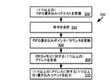
図3Aを参照すると、図示の方法300は、バッファを参照する書き込みリクエストの受信に応じて、ハードウェアバッファコントローラ208によって実行されてもよく、該書き込みリクエストは、バッファのエントリが実際に格納されるメモリデバイス104内のアドレスを含まないが、バッファの識別子を含む。
Referring to FIG. 3A, the illustrated
方法300は、バッファに対する1つ以上の書き込みリクエストを受信すること(302)と、ある期間中にバッファに対して受信された書き込みリクエストの数を特定するために書き込みリクエストを合計すること(304)とを含む。例えば、処理デバイス102、バス112、メモリデバイス104、又はハードウェアバッファ208の1クロック周期中に受信された書き込みリクエストの数がステップ304でカウントされてもよい。1クロック周期中に書き込みリクエストが受信されたバッファ毎に方法300のステップが実行されるように、上述したように、複数のバッファがハードウェアバッファコントローラ208によって実施されてもよい。図3A及び図3Bの目的で、“バッファ(the buffer)”は、図示の方法が実行されているバッファを指す。
方法300は、書き込みポインタ212及び書き込みカウンタ228の一方又は両方を更新すること(306)を含んでもよい。幾つかの実施形態では、これらの値の1つのみがバッファの状態を表すために使用される。例えば、ハードウェアバッファコントローラ208は、カウンタではなく、バッファの状態を特定するために書き込みポインタ212及び読み出しポインタ210のみを格納してもよい。その他では、カウンタ226、228のみが使用され、アドレスは、該カウンタとバッファの開始アドレスとから判定される。具体的には、ポインタ212及びカウンタ228を更新することは、クロック周期中に受信された書き込みリクエストの数ずつ、それら各々をインクリメントすることを含んでもよい。
方法300は、書き込みポインタ212の状態と302で受信された書き込みリクエストの数とに基づいてアドレスを生成すること(308)を更に含む。上述したように、ポインタの現在値が書き込みリクエストを受信すること(302)及び書き込みポインタ212を更新すること(306)よりも前にCであり、N個の書き込みリクエストが受信された場合、生成されるアドレスは、C、C+1、...、C+N−1であってもよく、ただし、Cは、次に書き込まれるアドレスを示す。Cが最も直近に書き込まれたアドレスを指し示す場合には、生成されるアドレスは、C+1、C+2...、C+Nである。アドレスは、範囲の形式、例えば、データ対<C,N−1>又は<C+1,N>の形式で生成されてもよく、ただし、一方の値が開始アドレスであり、他方の値が開始アドレスからのオフセットである。
方法300は、ステップ308で生成されたアドレスを含む1つ以上の書き込みコマンドであって、メモリデバイス104のうちの1つのメモリデバイス中の、1つ以上の書き込みコマンド内のアドレスにて、書き込みリクエストからデータの書き込みを引き起こす効果のある該書き込みコマンドをメモリサブシステム204へ出力すること(310)を更に含んでもよい。上述したように、N個の書き込みコマンドが、302で受信された書き込みリクエスト毎に、ステップ308で生成されたアドレスの内の1つを夫々含んで出力されてもよい(310)。或いは、ステップ308で生成されたN個全てのアドレス、又はN個全てのアドレスに渡るアドレスの範囲(例えば、開始アドレス及びオフセット)を指定する、ただ1つの書き込みコマンドが出力されてもよい(310)。書き込みコマンドは、それらがアドレス指定されるメモリデバイス104によってその後実行され、方法は終了する。
図3Bを参照すると、図示の方法312は、バッファを参照する読み出しリクエストであって、バッファの識別子を含み、バッファのエントリが実際に格納されるメモリデバイス104内のアドレスを含まない該読み出しリクエストの受信に応じてハードウェアバッファコントローラ208により実行されてもよい。 Referring to FIG. 3B, the illustrated method 312 is a read request that refers to a buffer, including the identifier of the buffer and not the address in the memory device 104 in which the entry of the buffer is actually stored. It may be executed by the hardware buffer controller 208 in response to reception.
方法312は、バッファに対する1つ以上の読み出しリクエストを受信すること(314)と、ある期間中にバッファに対して受信された読み出しリクエストの数を特定するために読み出しリクエストを合計すること316とを含む。例えば、処理デバイス102、バス112、メモリデバイス104、又はハードウェアバッファ208の1クロック周期中に受信された読み出しリクエストの数がステップ316でカウントされてもよい。上述したように、1クロック周期中に書き込みリクエストが受信されたバッファ毎に方法312のステップが実行されるように、複数のバッファがハードウェアバッファコントローラ208によって実施されてもよい。
Method 312 includes receiving one or more read requests to the buffer (314) and summing the read requests to determine the number of read requests received to the buffer over a period of time 316. Including. For example, the number of read requests received during one clock cycle of the processing device 102, the
方法312は、読み出しポインタ210及び読み出しカウンタ226の一方又は両方を更新すること(318)を含んでもよい。幾つかの実施形態では、これらの値の1つのみがバッファの状態を表すために使用される。例えば、ハードウェアバッファコントローラ208は、カウンタではなく、バッファの状態を特定するために書き込みポインタ212及び読み出しポインタ210のみを格納してもよい。その他では、カウンタ226、228のみが使用され、アドレスは、該カウンタとバッファの開始アドレスとから特定される。ポインタ210及びカウンタ226を更新すること(318)は、クロック周期中に受信された書き込みリクエストの数ずつ、それら各々をインクリメントすることを含んでもよい。
Method 312 may include updating one or both of the read pointer 210 and the read counter 226 (318). In some embodiments, only one of these values is used to represent the state of the buffer. For example, the hardware buffer controller 208 may store only the
方法312は、読み出しポインタ210の状態と314で受信された読み出しリクエストの数とに基づいてアドレスを生成すること(320)を更に含む。上述したように、ポインタの現在値が読み出しリクエストを受信すること(314)及び読み出しポインタ210を更新すること(318)よりも前にCであり、N個の読み出しリクエストが受信された場合、生成されるアドレスは、C、C+1、...、C+N−1であってもよく、ただし、Cは、次に書き込まれるアドレスを指し示す。Cが最も直近に読み出されたアドレスを指し示す場合には、生成されるアドレスは、C+1、C+2...、C+Nである。アドレスは、範囲の形式、例えば、データ対<C,N−1>又は<C+1,N>の形式で生成されてもよく、ただし、一方の値が開始アドレスであり、他方の値が開始アドレスからのオフセットである。 Method 312 further comprises generating an address (320) based on the state of the read pointer 210 and the number of read requests received at 314. As described above, if the current value of the pointer is C before receiving the read request (314) and updating the read pointer 210 (318) and N read requests are received, it will be generated. The addresses to be given are C, C + 1, ... .. .. , C + N-1, where C points to the address to be written next. If C points to the most recently read address, the generated addresses are C + 1, C + 2. .. .. , C + N. The address may be generated in the form of a range, eg, data pairs <C, N-1> or <C + 1, N>, where one value is the start address and the other value is the start address. Offset from.
方法312は、ステップ308で生成されたアドレスを含む1つ以上の読み出しコマンドであって、メモリデバイス104のうちの1つのメモリデバイスから、1つ以上の書き込みコマンド内のアドレスにてデータを抽出し、このデータを処理デバイス102へ返すことを引き起こす効果のある該読み出しコマンドをメモリサブシステム204へ出力すること(322)を更に含んでもよい。上述したように、N個の読み出しコマンドが、302で受信された読み出しリクエスト毎に、ステップ308で生成されたアドレスの内の1つを夫々含んで出力されてもよい(322)。或いは、ステップ308で生成されたN個全てのアドレス、又はN個全てのアドレスに渡るアドレスの範囲(例えば、開始アドレス及びオフセット)を指定するただ1つの読み出しコマンドが出力されてもよい(322)。読み出しコマンドは、それらがアドレス指定されるメモリデバイス104によってその後実行され、方法は終了する。
Method 312 is one or more read commands including the address generated in
方法300及び312は、実質的に同時に実行されてもよい。例えば、別々の読み出し及び書き込みのパイプラインがハードウェアバッファコントローラ208によって実施されてもよく、そうしたメモリアクセスコマンドは、読み出し及び書き込みのリクエスト両方に対して同時に生成され得る。ステップ310及び322からのメモリアクセスコマンドは、当該技術分野で周知の任意のコマンド実行スキームに従ってメモリサブシステム204によって順次バッファリングされ実行してもよい。
図4を参照すると、図示の方法400は、バッファの満杯、ほぼ満杯、空、及びほぼ空の状態を検出するためにハードウェアバッファコントローラ208によって実行されてもよい。方法400は、ハードウェアバッファコントローラ208によって制御されるバッファ(以後“バッファ(the buffer)”と称する)毎に実行されてもよい。
With reference to FIG. 4, the illustrated
方法400は、図3Aに関して上述したようなクロック周期中に書き込み命令を受信すること(302)と、クロック周期中に受信された書き込み命令を合計すること(304)とのステップを含んでもよく、又は方法400にそれらのステップが先行してもよい。合計するステップ304は、方法300及び方法400の両方に対して一回実行されてもよく、又は方法毎に別々に実行されてもよい。
方法400は更に、図3Bに関して上述したようなクロック周期中に書き込み命令を受信すること(314)と、クロック周期中に受信された書き込み命令を合計すること(316)とのステップを含んでもよく、又は方法400にそれらのステップが先行してもよい。合計するステップ316は、方法300及び方法400の両方に対して一回実行されてもよく、又は方法毎に別々に実行されてもよい。
方法400は、書き込みカウンタ238を更新すること(402)と、読み出しカウンタ236を更新すること(404)とを更に含んでもよい。上述したように、これは、クロック周期中に受信された書き込みリクエストの数を書き込みカウンタ238に加算することと、クロック周期中に受信された読み出しリクエストの数を読み出しカウンタ236に加算することとを含んでもよい。
方法400は、書き込みカウンタと読み出しカウンタの差を計算すること(406)を更に含んでもよい。読み出しが書き込みを超えるアンダーフロー状態ではないときは、書き込みカウンタと読み出しカウンタの差は正又はゼロであろう。幾つかの実施形態では、ステップ406の差分機能を回路により実行し、カウンタ236、238をレジスタにより格納することによって処理可能な最大数を超えることを回避するために、方法400の繰り返し毎に、書き込みカウンタは該差の値に等しく設定されてもよく、読み出しポインタはゼロに設定されてもよい。
方法400は、1つ以上のスレッドに関してステップ406で計算された差を評価することを含んでもよい。例えば、差が“ほぼ満杯”の閾値よりも大きいと408で検出された場合、“ほぼ満杯”のイベントが410で生成されてもよい。差が“ほぼ空”の閾値よりも小さいと412で検出された場合、“ほぼ空”のイベントが414で生成されてもよい。差がバッファのサイズよりも大きいと416で検出された場合、“バッファ満杯”のイベントが418で生成されてもよい。差がゼロであると420で検出された場合、“バッファ空”のイベントが生成されてもよい。ステップ408〜420の閾値は、並列パイプラインを使用して任意の順序で又は同時に評価されてもよい。
“ほぼ満杯”及び“ほぼ空”の閾値は、方法400の実行よりも前にハードワイヤード化またはプログラムされた所定の値でもよい。幾つかの実施形態では、“ほぼ満杯”及び“ほぼ空”の閾値は、実行するスレッドの数と、ほぼ満杯又はほぼ空の状態が存在すると検出される時とそのイベントに応じてスレッドがブロックされる時との間の遅延との関数であってもよい。例えば、書き込みリクエストを発行するようにプログラムされたM個のスレッドが実行され、イベントに応答してスレッドをブロックするために少なくともQのクロック周期かかる場合、“ほぼ満杯”の閾値は、S−Q*M−Rに等しく設定されることもあり、ただし、Sは、バッファのサイズであり、Rは、オーバーフローが生じないようにするためにゼロよりも大きい値である。このように、ほぼ満杯の状態が検出された場合、書き込みリクエストを発行し得るM個のスレッドのブロッキングが“ほぼ満杯”のイベントによりもたらされる前にバッファのオーバーフローは生じない。
The "nearly full" and "nearly empty" thresholds may be predetermined values hard-wired or programmed prior to execution of
同様に、読み出しリクエストを発行するようにプログラムされたM個のスレッドが実行されている場合、“ほぼ空”の閾値は、Q*M+Rに等しく設定されることもあり、ただし、Sは、バッファのサイズであり、Rは、アンダーフローが生じないようにするためにゼロよりも大きい値である。このように、ほぼ空の状態が検出された場合、読み出しリクエストを発行し得るM個のスレッドのブロッキングが“ほぼ空”のイベントによりもたらされる前にバッファのアンダーフローは生じない。 Similarly, if M threads programmed to issue read requests are running, the "nearly empty" threshold may be set equal to Q * M + R, where S is the buffer. And R is a value greater than zero to prevent underflow. Thus, when a nearly empty state is detected, there is no buffer underflow before the blocking of M threads that can issue read requests is brought about by the "nearly empty" event.
本発明は、その精神又は本質的特徴から離れることなくその他の特定の形態で具体化されてもよい。記述された実施形態は、全ての点で、例示あって限定的ではないと考慮されるべきである。発明の範囲は、それ故、前述の説明よりもむしろ添付の請求項の範囲によって示される。請求項の意図及び均等範囲内に入る全ての変更は、それらの範囲内に包含されるべきである。 The present invention may be embodied in other particular forms without departing from its spiritual or essential features. The described embodiments should be considered in all respects as being exemplary and not limiting. The scope of the invention is therefore indicated by the appended claims rather than the aforementioned description. The intent of the claims and all changes that fall within the equivalent range should be included within those ranges.
Claims (15)
前記メモリデバイスに結合され、前記実行可能なデータを抽出及び実行するように動作可能な処理デバイスを提供することと、
前記処理デバイスによって、バッファ初期化命令をアプリケーションから受信することと、
前記バッファ初期化命令に応じて、
前記処理デバイスによって、バッファとして前記メモリデバイスの一部分を割り当てること、
前記処理デバイスによって、前記メモリデバイスの前記一部分を参照するためにハードウェアバッファコントローラのある状態を引き起こすこと、及び
前記処理デバイスによって、前記ハードウェアバッファコントローラへの参照をアプリケーションへ返すことと、
前記処理デバイスによって、前記アプリケーションを実行することであって、前記アプリケーションから前記バッファにアクセスするためのリクエストを実行することを含み、前記リクエストが、前記ハードウェアバッファコントローラへの前記参照のみにアドレス指定され、前記メモリデバイスの前記一部分内の何れのアドレスも含まない、前記アプリケーションを実行することと、
前記リクエストに応じて、前記処理デバイスによって前記リクエストを前記ハードウェアバッファコントローラに入力することと、
前記ハードウェアバッファコントローラによって、前記リクエストを処理することであって、前記リクエストを処理することが前記リクエスト毎に、
前記ハードウェアバッファコントローラの前記状態に基づいて前記メモリデバイスの前記一部分内のアドレスを生成すること、
前記アドレスを含むメモリアクセス命令を前記メモリデバイスへ出力すること、及び
前記ハードウェアバッファコントローラの前記状態を更新すること
により行われる、前記リクエストを処理することと
を含む、方法。 To provide a memory device to store executable data,
To provide a processing device that is coupled to the memory device and can operate to extract and execute the executable data.
Receiving a buffer initialization instruction from the application by the processing device
In response to the buffer initialization instruction
Allocating a portion of the memory device as a buffer by the processing device,
The processing device causes some state of the hardware buffer controller to reference said portion of the memory device, and the processing device returns a reference to the hardware buffer controller to the application.
Executing the application by the processing device, including executing a request from the application to access the buffer, the request addressing only the reference to the hardware buffer controller. To run the application, which does not include any address within said portion of said memory device.
In response to the request, the processing device inputs the request to the hardware buffer controller, and
The hardware buffer controller is to process the request, and processing the request is to process the request for each request.
Generating an address within said portion of said memory device based on said state of the hardware buffer controller.
A method comprising outputting a memory access instruction including the address to the memory device and processing the request, which is performed by updating the state of the hardware buffer controller.
前記ハードウェアバッファコントローラの前記状態は読み出しポインタ及び書き込みポインタを含み、
前記ハードウェアバッファコントローラの前記状態を更新することは、前記リクエストの内の書き込みリクエスト毎に前記書き込みポインタをインクリメントすることを含み、
前記ハードウェアバッファコントローラの前記状態を更新することは、前記リクエストの内の読み出しリクエスト毎に前記読み出しポインタをインクリメントすることを含む、
請求項1に記載の方法。 The hardware buffer controller implements a first-in first-out (FIFO) buffer and
The state of the hardware buffer controller includes a read pointer and a write pointer.
Updating the state of the hardware buffer controller includes incrementing the write pointer for each write request in the request.
Updating the state of the hardware buffer controller includes incrementing the read pointer for each read request in the request.
The method according to claim 1.
前記読み出しポインタをインクリメントすることは、前記クロック周期中に受信された複数の読み出しリクエストの数を特定することと、前記複数の読み出しリクエストの前記数だけ前記読み出しポインタをインクリメントすることとを含む、
請求項2に記載の方法。 Incrementing the write pointer includes specifying the number of a plurality of write requests received in one clock cycle and incrementing the write pointer by the number of the plurality of write requests.
Incrementing the read pointer includes specifying the number of a plurality of read requests received during the clock cycle, and incrementing the read pointer by the number of the plurality of read requests.
The method according to claim 2.
前記ハードウェアバッファコントローラの前記状態に基づいて前記バッファ内の前記アドレスを生成することは、前記リクエストの内の読み出しリクエスト毎に前記読み出しポインタの現在値を出力することを含む、
請求項2に記載の方法。 Generating the address in the buffer based on the state of the hardware buffer controller includes outputting the current value of the write pointer for each write request in the request.
Generating the address in the buffer based on the state of the hardware buffer controller includes outputting the current value of the read pointer for each read request in the request.
The method according to claim 2.
前記処理デバイスによって、前記差が第1の閾値よりも少なくゼロではないと判定することと、
前記差が第1の閾値よりも少なくゼロではないと判定することに応じて、前記処理デバイスによって、前記バッファがほぼ空であることを示すイベントを出力することと、
前記バッファがほぼ空であることを示す前記イベントに応じて、前記処理デバイスによって、前記処理デバイスによって実行される1つ以上の実行スレッドが読み出しリクエストを生成することをブロックすることと
を更に含む、請求項4に記載の方法。 To calculate the difference between the amount of the write request and the amount of the read request by the processing device.
The processing device determines that the difference is less than the first threshold and is not zero.
In response to determining that the difference is less than the first threshold and not zero, the processing device outputs an event indicating that the buffer is nearly empty.
The processing device further comprises blocking one or more execution threads executed by the processing device from generating a read request in response to the event indicating that the buffer is nearly empty. The method according to claim 4.
前記ハードウェアバッファコントローラによって、前記差が第1の閾値よりも大きいと判定することと、
前記差が第1の閾値よりも大きいと判定することに応じて、前記ハードウェアバッファコントローラによって、前記バッファがほぼ満杯であることを示すイベントを出力することと、
前記バッファがほぼ満杯であることを示す前記イベントに応じて、前記処理デバイスによって、前記処理デバイスによって実行される1つ以上の実行スレッドが書き込みリクエストを生成することをブロックすることと
を更に含む、請求項4に記載の方法。 Using the hardware buffer controller to calculate the difference between the amount of write requests and the amount of read requests.
When the hardware buffer controller determines that the difference is larger than the first threshold value,
In response to determining that the difference is greater than the first threshold, the hardware buffer controller outputs an event indicating that the buffer is nearly full.
It further comprises blocking the processing device from generating write requests by one or more execution threads executed by the processing device in response to the event indicating that the buffer is nearly full. The method according to claim 4.
前記リクエストの内の複数の書き込みリクエストを集計することと、
前記複数の書き込みリクエストに対応する前記バッファ内の複数のアドレスを含む集計書き込み命令を前記メモリデバイスへ送信することと、
前記リクエストの内の複数の読み出しリクエストを集計することと、
前記複数の読み出しリクエストに対応する前記バッファ内の複数のアドレスを含む集計読み出し命令を前記メモリデバイスへ送信することと
を更に含み、
前記複数の書き込みリクエストは、前記リクエストの内のその他のリクエストが前記ハードウェアバッファコントローラに入力されるよりも前に、前記書き込みリクエストの内の少なくとも1つの書き込みリクエストが受信されるような重複方式で、複数の実行スレッドによって発行される、
請求項1に記載の方法。 Processing the request by the hardware buffer controller
Aggregating multiple write requests in the request and
Sending an aggregate write instruction including a plurality of addresses in the buffer corresponding to the plurality of write requests to the memory device, and
Aggregating multiple read requests among the requests and
Further including transmitting an aggregate read instruction including a plurality of addresses in the buffer corresponding to the plurality of read requests to the memory device.
The plurality of write requests are duplicated so that at least one of the write requests is received before the other requests in the request are input to the hardware buffer controller. , Issued by multiple execution threads,
The method according to claim 1.
前記処理デバイスによって、前記ハードウェアバッファコントローラの前記状態が閾条件を満たすと判定することと、
前記ハードウェアバッファコントローラの前記状態が前記閾条件を満たすと判定することに応じて、前記処理デバイスによって、前記ハードウェアバッファコントローラを参照する更なるリクエストを前記複数の実行スレッドが発行することをブロックすることと
を更に含む、請求項7に記載の方法。 To evaluate the state of the hardware buffer controller by the processing device,
The processing device determines that the state of the hardware buffer controller satisfies the threshold condition.
Blocking the processing device from issuing further requests to reference the hardware buffer controller by the processing device in response to determining that the state of the hardware buffer controller satisfies the threshold condition. The method of claim 7, further comprising doing.
処理デバイスと、
前記処理デバイスに動作可能に結合されたハードウェアバッファコントローラと
を含み、
前記処理デバイスは、前記メモリデバイスに結合され、前記実行可能なデータを抽出及び実行するように動作可能であり、前記処理デバイスは、バッファリクエストをアプリケーションから受信すること、並びに、前記バッファリクエストに応じて、
前記メモリデバイスの一部分を前記バッファリクエストのためのバッファとして割り当てること、
前記メモリデバイスの前記一部分を参照するために前記ハードウェアバッファコントローラのある状態を引き起こすこと、及び
前記ハードウェアバッファコントローラへの参照を前記アプリケーションへ返すこと
をするようにプログラムされ、
前記ハードウェアバッファコントローラは、前記処理デバイス及び前記メモリデバイスに結合され、前記ハードウェアバッファコントローラは、
前記メモリデバイス内の何れの格納位置に対する何れのアドレスも含まず、前記ハードウェアバッファコントローラのみにアドレス指定されたメモリアクセスリクエストを前記処理デバイスにより実行される前記アプリケーションから受信すること、
前記ハードウェアバッファコントローラの状態に基づいて、前記メモリデバイスの前記一部分内の生成アドレスを生成すること、
前記生成アドレスを含むメモリアクセス命令を前記メモリデバイスへ出力すること、
前記ハードウェアバッファコントローラの前記状態を更新すること
をするようにプログラムされる、
システム。 A memory device for storing executable data, and
Processing device and
Includes a hardware buffer controller operably coupled to said processing device.
The processing device is coupled to the memory device and is capable of operating to extract and execute the executable data, the processing device receiving a buffer request from an application and responding to the buffer request. hand,
Allocating a portion of the memory device as a buffer for the buffer request,
A program is programmed to cause some state of the hardware buffer controller to reference said portion of the memory device and to return a reference to the hardware buffer controller to the application.
The hardware buffer controller is coupled to the processing device and the memory device, and the hardware buffer controller is
Receiving a memory access request, which does not include any address for any storage location in the memory device and is addressed only to the hardware buffer controller , from the application executed by the processing device.
Generating a generated address within said portion of the memory device based on the state of the hardware buffer controller.
To output a memory access instruction including the generated address to the memory device,
Programmed to update the state of the hardware buffer controller,
system.
前記ハードウェアバッファコントローラは、前記リクエストの内の書き込みリクエスト毎に書き込みポインタをインクリメントすることによって、前記ハードウェアバッファコントローラの前記状態を更新するように更にプログラムされ、
前記ハードウェアバッファコントローラの前記状態を更新することは、前記リクエストの内の読み出しリクエスト毎に読み出しポインタをインクリメントすることを含み、
前記ハードウェアバッファコントローラは、1クロック周期中に受信された複数の書き込みリクエストの数を特定することと、前記複数の書き込みリクエストの前記数だけ前記書き込みポインタをインクリメントすることとによって、前記書き込みポインタをインクリメントするように更にプログラムされ、
前記ハードウェアバッファコントローラは、前記クロック周期中に受信された複数の読み出しリクエストの数を特定することと、前記複数の読み出しリクエストの前記数だけ前記読み出しポインタをインクリメントすることとによって、前記読み出しポインタをインクリメントするように更にプログラムされる、
請求項9に記載のシステム。 The state of the hardware buffer controller implements a first-in first-out (FIFO) buffer.
The hardware buffer controller is further programmed to update the state of the hardware buffer controller by incrementing the write pointer for each write request in the request.
Updating the state of the hardware buffer controller includes incrementing the read pointer for each read request in the request.
The hardware buffer controller sets the write pointer by specifying the number of a plurality of write requests received in one clock cycle and incrementing the write pointer by the number of the plurality of write requests. Further programmed to increment,
The hardware buffer controller sets the read pointer by specifying the number of a plurality of read requests received during the clock cycle and incrementing the read pointer by the number of the plurality of read requests. Further programmed to increment,
The system according to claim 9.
前記ハードウェアバッファコントローラは、前記リクエストの内の読み出しリクエスト毎に前記読み出しポインタの現在値を出力することによって、前記ハードウェアバッファコントローラの前記状態に基づいて、前記バッファに割り当てられた前記メモリデバイスの前記一部分内の前記生成アドレスを生成するように更にプログラムされる、
請求項10に記載のシステム。 By outputting the current value of the write pointer for each write request in the request, the hardware buffer controller of the memory device allocated to the buffer based on the state of the hardware buffer controller. Further programmed to generate the generated address within said portion
By outputting the current value of the read pointer for each read request in the request, the hardware buffer controller of the memory device allocated to the buffer based on the state of the hardware buffer controller. Further programmed to generate the generated address within the portion.
The system according to claim 10.
前記書き込みリクエストの量と前記読み出しリクエストの量との差を計算すること、及び
前記差が第1の閾値よりも少なくゼロではない場合に、前記バッファがほぼ空であることを示すイベントを出力すること
をするように更にプログラムされ、
前記処理デバイスは、前記バッファがほぼ空であることを示す前記イベントに応じて、前記処理デバイスによって実行される1つ以上の実行スレッドが読み出しリクエストを生成することをブロックするように更にプログラムされる、
請求項11に記載のシステム。 The hardware buffer controller is
Calculate the difference between the amount of write requests and the amount of read requests, and output an event indicating that the buffer is almost empty if the difference is less than the first threshold and is not zero. Further programmed to do things,
The processing device is further programmed to block one or more execution threads executed by the processing device from generating read requests in response to the event indicating that the buffer is nearly empty. ,
The system according to claim 11.
前記書き込みリクエストの量と前記読み出しリクエストの量との差を計算すること、及び
前記差が第2の閾値よりも大きい場合に、前記処理デバイスによって、前記バッファがほぼ満杯であることを示すイベントを出力すること
をするように更にプログラムされ、
前記処理デバイスは、前記バッファがほぼ満杯であることを示す前記イベントに応じて、前記処理デバイスによって実行される1つ以上の実行スレッドが書き込みリクエストを生成することをブロックするように更にプログラムされる、
請求項12に記載のシステム。 The hardware buffer controller is
Calculating the difference between the amount of write requests and the amount of read requests, and an event indicating that the buffer is nearly full by the processing device when the difference is greater than the second threshold. Further programmed to do output,
The processing device is further programmed to block one or more execution threads executed by the processing device from generating write requests in response to the event indicating that the buffer is nearly full. ,
The system according to claim 12.
前記リクエストの内の複数の書き込みリクエストを集計することと、
前記複数の書き込みリクエストに対応する前記バッファ内の複数のアドレスを含む集計書き込み命令を前記メモリデバイスへ送信することと、
前記リクエストの内の複数の読み出しリクエストを集計することと、
前記複数の読み出しリクエストに対応する前記バッファ内の複数のアドレスを含む集計読み出し命令を前記メモリデバイスへ送信することと
によって前記リクエストを処理するように更にプログラムされる、請求項9に記載のシステム。 The hardware Abba Tsu file controller,
Aggregating multiple write requests in the request and
Sending an aggregate write instruction including a plurality of addresses in the buffer corresponding to the plurality of write requests to the memory device, and
Aggregating multiple read requests among the requests and
9. The system of claim 9, further programmed to process the request by transmitting an aggregate read instruction containing the plurality of addresses in the buffer corresponding to the plurality of read requests to the memory device.
前記ハードウェアバッファコントローラの前記状態を評価すること、及び
前記ハードウェアバッファコントローラの前記状態が閾条件を満たす場合に、前記ハードウェアバッファコントローラを参照する更なるリクエストを前記複数の実行スレッドが発行することを、前記処理デバイスによってブロックすることを引き起こすこと
をするように更にプログラムされる、請求項14に記載のシステム。
The hardware buffer controller is in a duplicate manner such that at least one of the write requests is received before the other requests in the request are input to the hardware buffer controller. , The hardware buffer controller is programmed to receive the plurality of write requests from the plurality of execution threads executed by the processing device.
Evaluating the state of the hardware buffer controller, and when the state of the hardware buffer controller satisfies the threshold condition, the plurality of execution threads issue additional requests to refer to the hardware buffer controller. 14. The system of claim 14, further programmed to cause the processing device to block.
Applications Claiming Priority (3)
| Application Number | Priority Date | Filing Date | Title |
|---|---|---|---|
| US14/966,631 | 2015-12-11 | ||
| US14/966,631 US10585623B2 (en) | 2015-12-11 | 2015-12-11 | Software defined FIFO buffer for multithreaded access |
| PCT/US2016/066106 WO2017100748A1 (en) | 2015-12-11 | 2016-12-12 | Software defined fifo buffer for multithreaded access |
Publications (3)
| Publication Number | Publication Date |
|---|---|
| JP2019502201A JP2019502201A (en) | 2019-01-24 |
| JP2019502201A5 JP2019502201A5 (en) | 2020-01-09 |
| JP6884149B2 true JP6884149B2 (en) | 2021-06-09 |
Family
ID=59013408
Family Applications (1)
| Application Number | Title | Priority Date | Filing Date |
|---|---|---|---|
| JP2018529209A Active JP6884149B2 (en) | 2015-12-11 | 2016-12-12 | Software-defined FIFO buffer for multithreaded access |
Country Status (6)
| Country | Link |
|---|---|
| US (1) | US10585623B2 (en) |
| EP (1) | EP3387513A4 (en) |
| JP (1) | JP6884149B2 (en) |
| KR (1) | KR20180107091A (en) |
| CN (1) | CN108292162B (en) |
| WO (1) | WO2017100748A1 (en) |
Families Citing this family (7)
| Publication number | Priority date | Publication date | Assignee | Title |
|---|---|---|---|---|
| US10095408B2 (en) * | 2017-03-10 | 2018-10-09 | Microsoft Technology Licensing, Llc | Reducing negative effects of insufficient data throughput for real-time processing |
| CN108038006B (en) * | 2017-11-14 | 2022-02-08 | 北京小鸟看看科技有限公司 | Control method, device and system of head-mounted display device |
| KR102421103B1 (en) * | 2018-01-04 | 2022-07-14 | 에스케이하이닉스 주식회사 | Controller, memory system including the same and operating methods of the controller and the memory system |
| US10713746B2 (en) | 2018-01-29 | 2020-07-14 | Microsoft Technology Licensing, Llc | FIFO queue, memory resource, and task management for graphics processing |
| US11068308B2 (en) | 2018-03-14 | 2021-07-20 | Texas Instruments Incorporated | Thread scheduling for multithreaded data processing environments |
| US10719268B2 (en) * | 2018-06-29 | 2020-07-21 | Microsoft Technology Licensing, Llc | Techniques for safely and efficiently enqueueing and dequeueing data on a graphics processor |
| US10963385B2 (en) * | 2019-01-18 | 2021-03-30 | Silicon Motion Technology (Hong Kong) Limited | Method and apparatus for performing pipeline-based accessing management in a storage server with aid of caching metadata with cache module which is hardware pipeline module during processing object write command |
Family Cites Families (30)
| Publication number | Priority date | Publication date | Assignee | Title |
|---|---|---|---|---|
| JPH07118187B2 (en) | 1985-05-27 | 1995-12-18 | 松下電器産業株式会社 | First-in first-out storage |
| US4894797A (en) | 1986-11-17 | 1990-01-16 | Amp Incorporated | FIFO data storage system using PLA controlled multiplexer for concurrent reading and writing of registers by different controllers |
| US5581705A (en) | 1993-12-13 | 1996-12-03 | Cray Research, Inc. | Messaging facility with hardware tail pointer and software implemented head pointer message queue for distributed memory massively parallel processing system |
| KR0139887B1 (en) | 1994-02-17 | 1999-02-18 | 김광호 | Circuit for preventign a data contact of an image memory |
| US6115761A (en) | 1997-05-30 | 2000-09-05 | Lsi Logic Corporation | First-In-First-Out (FIFO) memories having dual descriptors and credit passing for efficient access in a multi-processor system environment |
| US5978868A (en) * | 1997-08-28 | 1999-11-02 | Cypress Semiconductor Corp. | System for generating buffer status flags by comparing read and write pointers and determining direction of progression of read pointer with respect to write pointer |
| US6044030A (en) | 1998-12-21 | 2000-03-28 | Philips Electronics North America Corporation | FIFO unit with single pointer |
| US6756986B1 (en) | 1999-10-18 | 2004-06-29 | S3 Graphics Co., Ltd. | Non-flushing atomic operation in a burst mode transfer data storage access environment |
| US20040098519A1 (en) | 2001-03-16 | 2004-05-20 | Hugo Cheung | Method and device for providing high data rate for a serial peripheral interface |
| US7206904B2 (en) * | 2002-03-20 | 2007-04-17 | Hewlett-Packard Development Company, L.P. | Method and system for buffering multiple requests from multiple devices to a memory |
| CN1201234C (en) * | 2003-03-28 | 2005-05-11 | 港湾网络有限公司 | Multichannel FILO data buffer storage devices |
| JP4505450B2 (en) | 2003-04-17 | 2010-07-21 | トムソン ライセンシング | Data request transmitting apparatus and process and corresponding products |
| US7181563B2 (en) | 2003-10-23 | 2007-02-20 | Lsi Logic Corporation | FIFO memory with single port memory modules for allowing simultaneous read and write operations |
| US8135915B2 (en) | 2004-03-22 | 2012-03-13 | International Business Machines Corporation | Method and apparatus for hardware assistance for prefetching a pointer to a data structure identified by a prefetch indicator |
| US6956776B1 (en) * | 2004-05-04 | 2005-10-18 | Xilinx, Inc. | Almost full, almost empty memory system |
| EP1811370A2 (en) | 2005-12-30 | 2007-07-25 | STMicroelectronics Pvt. Ltd. | A first-in first-out (FIFO) memory architecture providing multiport functionality |
| US9015375B2 (en) | 2006-04-11 | 2015-04-21 | Sigmatel, Inc. | Buffer controller, codec and methods for use therewith |
| JP2008293484A (en) * | 2007-04-27 | 2008-12-04 | Panasonic Corp | Buffer memory sharing apparatus |
| WO2009067538A1 (en) | 2007-11-19 | 2009-05-28 | Mentor Graphics Corporation | Dynamic pointer dereferencing and conversion to static hardware |
| GB2469299B (en) * | 2009-04-07 | 2011-02-16 | Imagination Tech Ltd | Ensuring consistency between a data cache and a main memory |
| CN101661386B (en) * | 2009-09-24 | 2013-03-20 | 成都市华为赛门铁克科技有限公司 | Multi-hardware thread processor and business processing method thereof |
| US8908564B2 (en) * | 2010-06-28 | 2014-12-09 | Avaya Inc. | Method for Media Access Control address learning and learning rate suppression |
| US9098462B1 (en) * | 2010-09-14 | 2015-08-04 | The Boeing Company | Communications via shared memory |
| US8949547B2 (en) * | 2011-08-08 | 2015-02-03 | Arm Limited | Coherency controller and method for data hazard handling for copending data access requests |
| JP5842206B2 (en) * | 2012-01-27 | 2016-01-13 | 株式会社トプスシステムズ | Processor core and multi-core processor system |
| US9542227B2 (en) | 2012-01-30 | 2017-01-10 | Nvidia Corporation | Parallel dynamic memory allocation using a lock-free FIFO |
| US20130198419A1 (en) * | 2012-01-30 | 2013-08-01 | Stephen Jones | Lock-free fifo |
| US9639371B2 (en) | 2013-01-29 | 2017-05-02 | Advanced Micro Devices, Inc. | Solution to divergent branches in a SIMD core using hardware pointers |
| WO2014142836A1 (en) * | 2013-03-13 | 2014-09-18 | Empire Technology Development, Llc | Memory allocation accelerator |
| US9672008B2 (en) * | 2014-11-24 | 2017-06-06 | Nvidia Corporation | Pausible bisynchronous FIFO |
-
2015
- 2015-12-11 US US14/966,631 patent/US10585623B2/en active Active
-
2016
- 2016-12-12 EP EP16874038.9A patent/EP3387513A4/en active Pending
- 2016-12-12 JP JP2018529209A patent/JP6884149B2/en active Active
- 2016-12-12 CN CN201680070274.5A patent/CN108292162B/en active Active
- 2016-12-12 KR KR1020187018862A patent/KR20180107091A/en not_active Application Discontinuation
- 2016-12-12 WO PCT/US2016/066106 patent/WO2017100748A1/en active Application Filing
Also Published As
| Publication number | Publication date |
|---|---|
| EP3387513A4 (en) | 2019-07-10 |
| WO2017100748A1 (en) | 2017-06-15 |
| JP2019502201A (en) | 2019-01-24 |
| US20170168755A1 (en) | 2017-06-15 |
| CN108292162B (en) | 2021-08-31 |
| US10585623B2 (en) | 2020-03-10 |
| EP3387513A1 (en) | 2018-10-17 |
| CN108292162A (en) | 2018-07-17 |
| KR20180107091A (en) | 2018-10-01 |
Similar Documents
| Publication | Publication Date | Title |
|---|---|---|
| JP6884149B2 (en) | Software-defined FIFO buffer for multithreaded access | |
| JP6888019B2 (en) | Memory access command transfer descriptor | |
| US10620994B2 (en) | Continuation analysis tasks for GPU task scheduling | |
| US10877757B2 (en) | Binding constants at runtime for improved resource utilization | |
| TWI489385B (en) | A computer-implemented method and a subsystem for free-fetching cache lines | |
| US20210192046A1 (en) | Resource Management Unit for Capturing Operating System Configuration States and Managing Malware | |
| US20200117623A1 (en) | Adaptive Interrupt Coalescing | |
| JP2019502201A5 (en) | ||
| US11782761B2 (en) | Resource management unit for capturing operating system configuration states and offloading tasks | |
| JP6974510B2 (en) | Methods, devices, devices and media for processing data | |
| US11630698B2 (en) | Resource management unit for capturing operating system configuration states and swapping memory content | |
| JP6966999B2 (en) | Hardware access counters and event generation to coordinate multithreaded processing |
Legal Events
| Date | Code | Title | Description |
|---|---|---|---|
| A521 | Request for written amendment filed |
Free format text: JAPANESE INTERMEDIATE CODE: A523 Effective date: 20191121 |
|
| A621 | Written request for application examination |
Free format text: JAPANESE INTERMEDIATE CODE: A621 Effective date: 20191121 |
|
| A977 | Report on retrieval |
Free format text: JAPANESE INTERMEDIATE CODE: A971007 Effective date: 20201125 |
|
| A131 | Notification of reasons for refusal |
Free format text: JAPANESE INTERMEDIATE CODE: A131 Effective date: 20201201 |
|
| A521 | Request for written amendment filed |
Free format text: JAPANESE INTERMEDIATE CODE: A523 Effective date: 20210226 |
|
| RD03 | Notification of appointment of power of attorney |
Free format text: JAPANESE INTERMEDIATE CODE: A7423 Effective date: 20210226 |
|
| TRDD | Decision of grant or rejection written | ||
| A01 | Written decision to grant a patent or to grant a registration (utility model) |
Free format text: JAPANESE INTERMEDIATE CODE: A01 Effective date: 20210413 |
|
| A61 | First payment of annual fees (during grant procedure) |
Free format text: JAPANESE INTERMEDIATE CODE: A61 Effective date: 20210511 |
|
| R150 | Certificate of patent or registration of utility model |
Ref document number: 6884149 Country of ref document: JP Free format text: JAPANESE INTERMEDIATE CODE: R150 |