JP6877447B2 - Surface acoustic wave device including a piezoelectric layer on a quartz substrate and its manufacturing method - Google Patents
Surface acoustic wave device including a piezoelectric layer on a quartz substrate and its manufacturing method Download PDFInfo
- Publication number
- JP6877447B2 JP6877447B2 JP2018539290A JP2018539290A JP6877447B2 JP 6877447 B2 JP6877447 B2 JP 6877447B2 JP 2018539290 A JP2018539290 A JP 2018539290A JP 2018539290 A JP2018539290 A JP 2018539290A JP 6877447 B2 JP6877447 B2 JP 6877447B2
- Authority
- JP
- Japan
- Prior art keywords
- carrier substrate
- piezoelectric layer
- axis
- quartz
- quartz carrier
- Prior art date
- Legal status (The legal status is an assumption and is not a legal conclusion. Google has not performed a legal analysis and makes no representation as to the accuracy of the status listed.)
- Active
Links
- VYPSYNLAJGMNEJ-UHFFFAOYSA-N silicon dioxide Inorganic materials O=[Si]=O VYPSYNLAJGMNEJ-UHFFFAOYSA-N 0.000 title claims description 168
- 239000000758 substrate Substances 0.000 title claims description 167
- 238000010897 surface acoustic wave method Methods 0.000 title claims description 159
- 239000010453 quartz Substances 0.000 title claims description 145
- 238000004519 manufacturing process Methods 0.000 title claims description 27
- 239000013078 crystal Substances 0.000 claims description 36
- 229910052814 silicon oxide Inorganic materials 0.000 claims description 21
- WSMQKESQZFQMFW-UHFFFAOYSA-N 5-methyl-pyrazole-3-carboxylic acid Chemical compound CC1=CC(C(O)=O)=NN1 WSMQKESQZFQMFW-UHFFFAOYSA-N 0.000 claims description 10
- 230000035945 sensitivity Effects 0.000 claims description 10
- 238000001914 filtration Methods 0.000 claims description 7
- ZOXJGFHDIHLPTG-UHFFFAOYSA-N Boron Chemical group [B] ZOXJGFHDIHLPTG-UHFFFAOYSA-N 0.000 claims description 3
- KRHYYFGTRYWZRS-UHFFFAOYSA-M Fluoride anion Chemical compound [F-] KRHYYFGTRYWZRS-UHFFFAOYSA-M 0.000 claims description 3
- 229910052796 boron Inorganic materials 0.000 claims description 3
- 239000002019 doping agent Substances 0.000 claims description 3
- 230000001902 propagating effect Effects 0.000 claims 1
- 239000000463 material Substances 0.000 description 30
- 238000000034 method Methods 0.000 description 29
- 230000008569 process Effects 0.000 description 24
- 239000010408 film Substances 0.000 description 21
- 230000008878 coupling Effects 0.000 description 18
- 238000010168 coupling process Methods 0.000 description 18
- 238000005859 coupling reaction Methods 0.000 description 18
- 229910052751 metal Inorganic materials 0.000 description 15
- 239000002184 metal Substances 0.000 description 15
- 229910013641 LiNbO 3 Inorganic materials 0.000 description 7
- 230000008901 benefit Effects 0.000 description 6
- 230000005855 radiation Effects 0.000 description 6
- 238000013461 design Methods 0.000 description 5
- 238000002347 injection Methods 0.000 description 5
- 239000007924 injection Substances 0.000 description 5
- 238000004088 simulation Methods 0.000 description 5
- XUIMIQQOPSSXEZ-UHFFFAOYSA-N Silicon Chemical compound [Si] XUIMIQQOPSSXEZ-UHFFFAOYSA-N 0.000 description 4
- 230000008859 change Effects 0.000 description 4
- 230000007547 defect Effects 0.000 description 4
- GQYHUHYESMUTHG-UHFFFAOYSA-N lithium niobate Chemical compound [Li+].[O-][Nb](=O)=O GQYHUHYESMUTHG-UHFFFAOYSA-N 0.000 description 4
- 229910052710 silicon Inorganic materials 0.000 description 4
- 239000010703 silicon Substances 0.000 description 4
- 238000003780 insertion Methods 0.000 description 3
- 230000037431 insertion Effects 0.000 description 3
- 150000002500 ions Chemical class 0.000 description 3
- 230000004044 response Effects 0.000 description 3
- 238000013459 approach Methods 0.000 description 2
- 230000005684 electric field Effects 0.000 description 2
- 239000005350 fused silica glass Substances 0.000 description 2
- 238000000227 grinding Methods 0.000 description 2
- 238000005468 ion implantation Methods 0.000 description 2
- 239000004065 semiconductor Substances 0.000 description 2
- JBRZTFJDHDCESZ-UHFFFAOYSA-N AsGa Chemical compound [As]#[Ga] JBRZTFJDHDCESZ-UHFFFAOYSA-N 0.000 description 1
- 229910001218 Gallium arsenide Inorganic materials 0.000 description 1
- 229910052581 Si3N4 Inorganic materials 0.000 description 1
- 238000007792 addition Methods 0.000 description 1
- 230000000903 blocking effect Effects 0.000 description 1
- 230000015556 catabolic process Effects 0.000 description 1
- 239000000919 ceramic Substances 0.000 description 1
- 238000006731 degradation reaction Methods 0.000 description 1
- 239000003989 dielectric material Substances 0.000 description 1
- 238000006073 displacement reaction Methods 0.000 description 1
- 230000000694 effects Effects 0.000 description 1
- 239000011521 glass Substances 0.000 description 1
- 239000012528 membrane Substances 0.000 description 1
- NVLSIZITFJRWPY-ONEGZZNKSA-N n,n-dimethyl-4-[(e)-2-(4-nitrophenyl)ethenyl]aniline Chemical compound C1=CC(N(C)C)=CC=C1\C=C\C1=CC=C([N+]([O-])=O)C=C1 NVLSIZITFJRWPY-ONEGZZNKSA-N 0.000 description 1
- 238000005457 optimization Methods 0.000 description 1
- TWNQGVIAIRXVLR-UHFFFAOYSA-N oxo(oxoalumanyloxy)alumane Chemical compound O=[Al]O[Al]=O TWNQGVIAIRXVLR-UHFFFAOYSA-N 0.000 description 1
- 238000002161 passivation Methods 0.000 description 1
- 238000005498 polishing Methods 0.000 description 1
- 238000012545 processing Methods 0.000 description 1
- 239000010980 sapphire Substances 0.000 description 1
- 229910052594 sapphire Inorganic materials 0.000 description 1
- 238000000926 separation method Methods 0.000 description 1
- HQVNEWCFYHHQES-UHFFFAOYSA-N silicon nitride Chemical compound N12[Si]34N5[Si]62N3[Si]51N64 HQVNEWCFYHHQES-UHFFFAOYSA-N 0.000 description 1
- 239000010409 thin film Substances 0.000 description 1
- 238000012546 transfer Methods 0.000 description 1
- 230000007704 transition Effects 0.000 description 1
Images


Classifications
-
- H—ELECTRICITY
- H03—ELECTRONIC CIRCUITRY
- H03H—IMPEDANCE NETWORKS, e.g. RESONANT CIRCUITS; RESONATORS
- H03H9/00—Networks comprising electromechanical or electro-acoustic devices; Electromechanical resonators
- H03H9/02—Details
- H03H9/02535—Details of surface acoustic wave devices
- H03H9/02543—Characteristics of substrate, e.g. cutting angles
- H03H9/02574—Characteristics of substrate, e.g. cutting angles of combined substrates, multilayered substrates, piezoelectrical layers on not-piezoelectrical substrate
-
- H—ELECTRICITY
- H03—ELECTRONIC CIRCUITRY
- H03H—IMPEDANCE NETWORKS, e.g. RESONANT CIRCUITS; RESONATORS
- H03H3/00—Apparatus or processes specially adapted for the manufacture of impedance networks, resonating circuits, resonators
- H03H3/007—Apparatus or processes specially adapted for the manufacture of impedance networks, resonating circuits, resonators for the manufacture of electromechanical resonators or networks
- H03H3/08—Apparatus or processes specially adapted for the manufacture of impedance networks, resonating circuits, resonators for the manufacture of electromechanical resonators or networks for the manufacture of resonators or networks using surface acoustic waves
-
- H—ELECTRICITY
- H03—ELECTRONIC CIRCUITRY
- H03H—IMPEDANCE NETWORKS, e.g. RESONANT CIRCUITS; RESONATORS
- H03H9/00—Networks comprising electromechanical or electro-acoustic devices; Electromechanical resonators
- H03H9/02—Details
- H03H9/02535—Details of surface acoustic wave devices
- H03H9/02543—Characteristics of substrate, e.g. cutting angles
- H03H9/02551—Characteristics of substrate, e.g. cutting angles of quartz substrates
-
- H—ELECTRICITY
- H03—ELECTRONIC CIRCUITRY
- H03H—IMPEDANCE NETWORKS, e.g. RESONANT CIRCUITS; RESONATORS
- H03H9/00—Networks comprising electromechanical or electro-acoustic devices; Electromechanical resonators
- H03H9/46—Filters
- H03H9/54—Filters comprising resonators of piezoelectric or electrostrictive material
- H03H9/56—Monolithic crystal filters
- H03H9/562—Monolithic crystal filters comprising a ceramic piezoelectric layer
-
- H—ELECTRICITY
- H03—ELECTRONIC CIRCUITRY
- H03H—IMPEDANCE NETWORKS, e.g. RESONANT CIRCUITS; RESONATORS
- H03H9/00—Networks comprising electromechanical or electro-acoustic devices; Electromechanical resonators
- H03H9/46—Filters
- H03H9/64—Filters using surface acoustic waves
Landscapes
- Physics & Mathematics (AREA)
- Acoustics & Sound (AREA)
- Engineering & Computer Science (AREA)
- Manufacturing & Machinery (AREA)
- Chemical & Material Sciences (AREA)
- Ceramic Engineering (AREA)
- Crystallography & Structural Chemistry (AREA)
- Surface Acoustic Wave Elements And Circuit Networks Thereof (AREA)
Description
本開示は、弾性表面波(SAW)デバイスに関する。 The present disclosure relates to surface acoustic wave (SAW) devices.
弾性表面波(SAW)共振子、及びSAWフィルタなどの、SAWデバイスは、高周波(RF)フィルタなどの多くのアプリケーションにおいて使用される。たとえば、SAWフィルタは、第2世代(2G)、第3世代(3G)、及び第4世代(4G)無線受信器のフロントエンド、デュプレクサ、及び受信フィルタにおいて一般に使用される。SAWフィルタの普及は、SAWフィルタが良好な除去により低い挿入損失を示し、広帯域幅を達成することが可能であり、従来のキャビティ及びセラミックフィルタの大きさのごく一部である、という事実に少なくとも部分的に起因する。任意の電子機器と同様に、SAWデバイスの性能は、システムの全体的な性能に影響を与えることが可能である重要なパラメータである。この点について、高性能のSAWデバイスが必要とされる。 SAW devices, such as surface acoustic wave (SAW) resonators, and SAW filters, are used in many applications such as radio frequency (RF) filters. For example, SAW filters are commonly used in front-ends, duplexers, and receive filters for 2nd generation (2G), 3rd generation (3G), and 4th generation (4G) radio receivers. The widespread use of SAW filters is at least due to the fact that SAW filters exhibit low insertion loss due to good removal, are capable of achieving wide bandwidth, and are only a small part of the size of conventional cavities and ceramic filters. Partially caused. As with any electronic device, the performance of a SAW device is an important parameter that can affect the overall performance of the system. In this regard, a high-performance SAW device is required.
弾性表面波(SAW)デバイス及びその製造方法の実施形態を開示する。いくつかの実施形態において、SAWデバイスは、石英キャリア基板、この石英キャリア基板の表面上に圧電層、及び石英キャリア基板に対向する圧電層の表面上に少なくとも1つの交差指電極を含む。特に、本明細書に使用されるように、「石英」は、非晶質である、溶融シリカ(ときには溶融シリカ石英と称される)とは対照的に単結晶石英である。いくつかの実施形態において、圧電層の厚さは、少なくとも1つの交差指電極のトランスデューサ電極周期の4倍未満である。他の実施形態において、圧電層の厚さは、少なくとも1つの交差指電極のトランスデューサ電極周期の2倍未満である。キャリア基板上に圧電層を使用することは、バルク(すなわち、基板)内への音響放射を抑制することにより、SAWデバイスの性能を向上させる。さらに、キャリア基板に石英を利用することにより、わずかな粘性損失、わずかな誘電率、及びわずかな温度感度のさらなる利点を達成する。さらに、ケイ素と比較されるように、キャリア基板への石英の使用は、抵抗損失をなくす。 An embodiment of a surface acoustic wave (SAW) device and a method for manufacturing the same is disclosed. In some embodiments, the SAW device comprises a quartz carrier substrate, a piezoelectric layer on the surface of the quartz carrier substrate, and at least one intersecting finger electrode on the surface of the piezoelectric layer facing the quartz carrier substrate. In particular, as used herein, "quartz" is single crystal quartz in contrast to fused silica (sometimes referred to as fused silica quartz), which is amorphous. In some embodiments, the thickness of the piezoelectric layer is less than four times the transducer electrode period of at least one crossed finger electrode. In other embodiments, the thickness of the piezoelectric layer is less than twice the transducer electrode period of at least one crossed finger electrode. The use of a piezoelectric layer on a carrier substrate improves the performance of SAW devices by suppressing acoustic radiation into the bulk (ie, substrate). In addition, the use of quartz for the carrier substrate achieves the additional benefits of low viscosity loss, low dielectric constant, and low temperature sensitivity. Moreover, the use of quartz in the carrier substrate, as compared to silicon, eliminates resistance loss.
いくつかの実施形態において、少なくとも1つの交差指電極の伝搬方向は、石英キャリア基板の水晶振動子のz軸または−z軸に関して10度未満の角度を形成する。さらに、いくつかの実施形態において、圧電層は、タンタル酸リチウム(LiTaO3)(ときには本明細書において「LT」と称される)から形成され、このタンタル酸リチウムは、たとえば、水晶振動子のz軸とLT結晶のx軸のアライメントを取るように結合することにより可能である、YからY+60度の間の配向、及びLT結晶のx軸沿いの伝搬を有する。さらに、いくつかの実施形態において、圧電層の厚さは、少なくとも1つの交差指電極のトランスデューサ電極周期の60%未満である。 In some embodiments, the propagation direction of at least one cross-finger electrode forms an angle of less than 10 degrees with respect to the z-axis or −z-axis of the crystal unit of the quartz carrier substrate. Further, in some embodiments, the piezoelectric layer is formed from lithium tantalate (LiTaO 3 ) (sometimes referred to herein as "LT"), which lithium tantalate is, for example, in a crystal oscillator. It has an orientation between Y and Y + 60 degrees, and propagation along the x-axis of the LT crystal, which is possible by combining the z-axis with the x-axis of the LT crystal. Moreover, in some embodiments, the thickness of the piezoelectric layer is less than 60% of the transducer electrode period of at least one crossed finger electrode.
いくつかの実施形態において、石英キャリア基板の法線は、石英キャリア基板の水晶振動子のx軸またはy軸沿いに配向される。さらに、いくつかの実施形態において、圧電層の厚さは、少なくとも1つの交差指電極のトランスデューサ電極周期の30%から50%の間にある。 In some embodiments, the normals of the quartz carrier substrate are oriented along the x-axis or y-axis of the crystal unit of the quartz carrier substrate. Moreover, in some embodiments, the thickness of the piezoelectric layer is between 30% and 50% of the transducer electrode period of at least one crossed finger electrode.
他の実施形態において、石英キャリア基板の法線は、石英キャリア基板の水晶振動子のx軸に関して30度から55度の間の角度を形成する。さらに、いくつかの実施形態において、圧電層の厚さは、少なくとも1つの交差指電極のトランスデューサ電極周期の20%から40%の間にある。 In another embodiment, the normals of the quartz carrier substrate form an angle between 30 and 55 degrees with respect to the x-axis of the crystal unit of the quartz carrier substrate. Moreover, in some embodiments, the thickness of the piezoelectric layer is between 20% and 40% of the transducer electrode period of at least one crossed finger electrode.
いくつかの実施形態において、圧電層は、YからY+60度の間の配向を有するLTから形成される。他の実施形態において、圧電層は、Y−20度からY+60度の間の配向を有するニオブ酸リチウム(LiNbO3)から形成される。 In some embodiments, the piezoelectric layer is formed from an LT having an orientation between Y and Y + 60 degrees. In another embodiment, the piezoelectric layer is formed from lithium niobate (LiNbO 3 ) with an orientation between Y-20 degrees and Y + 60 degrees.
いくつかの実施形態において、SAWデバイスは、石英キャリア基板と圧電層との間の石英キャリア基板の表面上に1層以上の追加の層をさらに含む。さらに、いくつかの実施形態において、1層以上の追加の層は、1層以上の誘電体層を含む。いくつかの実施形態において、1層以上の誘電体層は、少なくとも1層の酸化ケイ素を含む。 In some embodiments, the SAW device further comprises one or more additional layers on the surface of the quartz carrier substrate between the quartz carrier substrate and the piezoelectric layer. Further, in some embodiments, the one or more additional layers include one or more dielectric layers. In some embodiments, the one or more dielectric layers comprises at least one layer of silicon oxide.
いくつかの実施形態において、少なくとも1つの交差指電極は、1層以上の誘電体層の内側に埋め込まれる。いくつかの実施形態において、1層以上の誘電体層は、酸化ケイ素を含む。 In some embodiments, at least one cross-finger electrode is embedded inside one or more dielectric layers. In some embodiments, the one or more dielectric layers comprises silicon oxide.
いくつかの実施形態において、SAWデバイスは、圧電層に対向する少なくとも1つの交差指電極の表面上に1層以上の誘電体層をさらに含む。 In some embodiments, the SAW device further comprises one or more dielectric layers on the surface of at least one intersecting finger electrode facing the piezoelectric layer.
いくつかの実施形態において、SAWデバイスは、石英キャリア基板と圧電層との間の石英キャリア基板の表面上に少なくとも1層の酸化ケイ素をさらに含み、そこで少なくとも1層の酸化ケイ素は、その温度感度を低下させるようにドーピングされる。いくつかの実施形態において、少なくとも1層の酸化ケイ素は、フッ化物またはホウ素原子を含有するドーパントによりドーピングされる。 In some embodiments, the SAW device further comprises at least one layer of silicon oxide on the surface of the quartz carrier substrate between the quartz carrier substrate and the piezoelectric layer, wherein at least one layer of silicon oxide is its temperature sensitivity. Is doped to reduce. In some embodiments, at least one layer of silicon oxide is doped with a fluoride or a dopant containing a boron atom.
いくつかの実施形態において、SAWデバイスは、SAW共振子である。 In some embodiments, the SAW device is a SAW resonator.
またフィルタリング回路の実施形態を開示する。一般に、フィルタリング回路は、上記の実施形態のうちのいずれかに従い1つ以上のSAWフィルタを含む。 Also disclosed are embodiments of filtering circuits. Generally, the filtering circuit includes one or more SAW filters according to any of the above embodiments.
いくつかの実施形態において、フィルタリング回路は、石英キャリア基板、石英キャリア基板の表面上に圧電層、及び石英キャリア基板に対向する圧電層の表面上に少なくとも1つの交差指電極を含むSAW共振子を備える。いくつかの実施形態において、圧電層の厚さは、少なくとも1つの交差指電極のトランスデューサ電極周期の4倍未満である。他の実施形態において、圧電層の厚さは、少なくとも1つの交差指電極のトランスデューサ電極周期の2倍未満である。 In some embodiments, the filtering circuit comprises a quartz carrier substrate, a piezoelectric layer on the surface of the quartz carrier substrate, and a SAW resonator comprising at least one intersecting finger electrode on the surface of the piezoelectric layer facing the quartz carrier substrate. Be prepared. In some embodiments, the thickness of the piezoelectric layer is less than four times the transducer electrode period of at least one crossed finger electrode. In other embodiments, the thickness of the piezoelectric layer is less than twice the transducer electrode period of at least one crossed finger electrode.
いくつかの実施形態において、フィルタリング回路は、ラダー型フィルタを含み、このラダー型フィルタは、石英キャリア基板と、石英キャリア基板の表面上に圧電層と、石英キャリア基板に対向する圧電層の表面上に少なくとも1つの交差指電極とを各含む複数のSAW共振子を備える。いくつかの実施形態において、圧電層の厚さは、少なくとも1つの交差指電極のトランスデューサ電極周期の4倍未満である。他の実施形態において、圧電層の厚さは、少なくとも1つの交差指電極のトランスデューサ電極周期の2倍未満である。 In some embodiments, the filtering circuit comprises a rudder filter, which is a quartz carrier substrate, a piezoelectric layer on the surface of the quartz carrier substrate, and a piezoelectric layer on the surface facing the quartz carrier substrate. It is provided with a plurality of SAW resonators, each including at least one intersecting finger electrode. In some embodiments, the thickness of the piezoelectric layer is less than four times the transducer electrode period of at least one crossed finger electrode. In other embodiments, the thickness of the piezoelectric layer is less than twice the transducer electrode period of at least one crossed finger electrode.
いくつかの実施形態において、フィルタリング回路は、2つのグレーティング間に複数のトランスデューサを関連付けることにより形成される石英キャリア基板、石英キャリア基板の表面上に圧電層、及び石英キャリア基板に対向する圧電層の表面上に少なくとも1つの交差指電極を各含む複数のSAW共振子を備える結合型共振子フィルタ(CRF)を含む。いくつかの実施形態において、圧電層の厚さは、少なくとも1つの交差指電極のトランスデューサ電極周期の4倍未満である。他の実施形態において、圧電層の厚さは、少なくとも1つの交差指電極のトランスデューサ電極周期の2倍未満である。いくつかの実施形態において、フィルタリング回路は、CRFを含む、少なくとも1つのCRFのカスケード、及び直列に、または並列に接続される少なくとも1つの追加のSAW共振子をさらに備える。 In some embodiments, the filtering circuit is a quartz carrier substrate formed by associating a plurality of transducers between two gratings, a piezoelectric layer on the surface of the quartz carrier substrate, and a piezoelectric layer facing the quartz carrier substrate. A coupled resonator filter (CRF) comprising a plurality of SAW resonators each including at least one intersecting finger electrode on the surface is included. In some embodiments, the thickness of the piezoelectric layer is less than four times the transducer electrode period of at least one crossed finger electrode. In other embodiments, the thickness of the piezoelectric layer is less than twice the transducer electrode period of at least one crossed finger electrode. In some embodiments, the filtering circuit further comprises a cascade of at least one CRF, including a CRF, and at least one additional SAW resonator connected in series or in parallel.
またSAWデバイスを製造する方法の実施形態を開示する。いくつかの実施形態において、SAWデバイスを製造する方法は、石英キャリア基板を提供し、石英キャリア基板の表面上に圧電層を提供し、石英キャリア基板に対向する圧電層の表面上に少なくとも1つの交差指電極を提供することを備える。いくつかの実施形態において、圧電層の厚さは、少なくとも1つの交差指電極のトランスデューサ電極周期の4倍未満である。他の実施形態において、圧電層の厚さは、少なくとも1つの交差指電極のトランスデューサ電極周期の2倍未満である。 Also disclosed are embodiments of methods for manufacturing SAW devices. In some embodiments, the method of manufacturing a SAW device provides a quartz carrier substrate, a piezoelectric layer on the surface of the quartz carrier substrate, and at least one on the surface of the piezoelectric layer facing the quartz carrier substrate. Provided to provide cross-finger electrodes. In some embodiments, the thickness of the piezoelectric layer is less than four times the transducer electrode period of at least one crossed finger electrode. In other embodiments, the thickness of the piezoelectric layer is less than twice the transducer electrode period of at least one crossed finger electrode.
いくつかの実施形態において、石英キャリア基板の表面上に圧電層を提供することは、石英キャリア基板の表面上に圧電材料を付着させ、圧電材料を加工して圧電層の所望の厚さへ圧電材料の厚さを減少させることにより、圧電層を提供することを備える。 In some embodiments, providing a piezoelectric layer on the surface of a quartz carrier substrate allows the piezoelectric material to adhere to the surface of the quartz carrier substrate and process the piezoelectric material to be piezoelectric to the desired thickness of the piezoelectric layer. It comprises providing a piezoelectric layer by reducing the thickness of the material.
いくつかの実施形態において、石英キャリア基板の表面上に圧電層を提供することは、圧電材料の表面内へのイオン注入を実行することにより、圧電材料の損傷部分を形成し、石英キャリア基板の表面上に圧電材料を付着させ、圧電材料を加工して圧電材料の損傷部分を除去することにより、圧電層を提供することを備える。 In some embodiments, providing a piezoelectric layer on the surface of a quartz carrier substrate forms a damaged portion of the piezoelectric material by performing ion implantation into the surface of the piezoelectric material and the quartz carrier substrate. It comprises providing a piezoelectric layer by adhering a piezoelectric material on the surface and processing the piezoelectric material to remove damaged portions of the piezoelectric material.
いくつかの実施形態において、方法は、石英キャリア基板と圧電層と間の石英キャリア基板の表面上に1層以上の追加の層を提供することをさらに備える。 In some embodiments, the method further comprises providing one or more additional layers on the surface of the quartz carrier substrate between the quartz carrier substrate and the piezoelectric layer.
当業者は、本開示の範囲を理解し、添付の描写する図面と関連付けて、以下の発明を実施するための形態を読解した後に、その追加の態様を実現するであろう。 One of ordinary skill in the art will realize the additional aspects after understanding the scope of the present disclosure and reading the embodiments for carrying out the following invention in connection with the accompanying depictions.
本明細書の一部に援用され、これを形成する添付の描写する図面は、本開示のいくつかの態様を図示し、説明と併せて、本開示の原理を説明するために役立つ。 The accompanying descriptive drawings, which are incorporated and forming, which are incorporated herein by reference, illustrate some aspects of the disclosure and, in conjunction with the description, serve to illustrate the principles of the disclosure.
以下に記載される実施形態は、当業者が実施形態を実施することを可能にするために必要な情報を表現し、実施形態を実施する最良なモードを図示する。添付の描写する図面に照らして下記の説明を読解すると、当業者は、本開示の概念を理解し、特に本明細書に指定されないこれらの概念の適用を認識するであろう。これらの概念及び適用が本開示の範囲、及び添付の特許請求の範囲内に入ることを理解するであろう。 The embodiments described below represent the information necessary to enable one of ordinary skill in the art to implement the embodiments and illustrate the best modes of implementing the embodiments. Upon reading the following description in the light of the accompanying drawings, one of ordinary skill in the art will understand the concepts of the present disclosure and will recognize the application of these concepts not specifically specified herein. You will understand that these concepts and applications fall within the scope of this disclosure and the appended claims.
用語、第一、第二などがさまざまな要素を記述するために本明細書に使用されることができるが、これらの要素がこれらの用語により限定されるべきではないことを理解するであろう。これらの用語は、一方の要素を他方の要素から区別するためにのみ使用される。たとえば、本開示の範囲から逸脱することなく、第一要素は、第二要素と称されることが可能であり、同様に、第二要素は、第一要素と称されることが可能である。本明細書に使用されるように、用語「及び/または」は、関連した、列挙される項目のうちの1つ以上のいずれかの、及びすべての組み合わせを含む。 It will be understood that terms, first, second, etc. can be used herein to describe various elements, but these elements should not be limited by these terms. .. These terms are used only to distinguish one element from the other. For example, without departing from the scope of the present disclosure, the first element can be referred to as the second element, and similarly, the second element can be referred to as the first element. .. As used herein, the term "and / or" includes any, and all combinations of one or more of the related, listed items.
一方の要素が他方の要素に「接続される」、若しくは「結合される」と称されるときに、それが残りの要素に直接に接続される、若しくは結合されることが可能である、または複数の介在要素が存在することができることも理解するであろう。対照的に、一方の要素が他方の要素へ「直接に接続される」、または「直接に結合される」と称されるときに、介在要素が存在しない。 When one element is referred to as "connected" or "combined" to the other element, it can be directly connected to, or can be combined with, the other element. You will also understand that there can be multiple intervening elements. In contrast, there are no intervening elements when one element is referred to as "directly connected" or "directly connected" to the other element.
用語「上部の」、「下部の」、「基部の」、「中間の」、「中央の」、「最上部の」、及び同様のものがさまざまな要素を記述するために本明細書に使用されることができ、これらの要素がこれらの用語により限定されるべきではないことを理解するであろう。これらの用語は、一方の要素を他方から区別するためにのみ使用される。たとえば、本開示の範囲から逸脱することなく、第一要素は、「上部」要素と称されることが可能であり、同様に、第二要素は、これらの要素の相対的な位置に起因して「上部」要素と称されることが可能である。 The terms "top", "bottom", "base", "middle", "center", "top", and the like are used herein to describe various elements. It can be understood that these elements should not be limited by these terms. These terms are used only to distinguish one element from the other. For example, without departing from the scope of the present disclosure, the first element can be referred to as the "upper" element, and similarly, the second element is due to the relative position of these elements. Can be referred to as the "upper" element.
本明細書に使用される専門用語は、特定の実施形態のみを説明するためのものであり、本開示の制限であることを意図されない。本明細書に使用されるように、単数形「a」、「an」、及び「the」は、文脈が明確に別段に示さない限り、複数形をも含むことを意図される。本明細書に使用されるときに、用語「comprises(を含む)」、「comprising(を含むこと)」、「includes(を含む)」、及び/または「including(を含むこと)」が記載された特徴、整数、ステップ、操作、要素、及び/または構成要素の存在を明示するが、1つ以上の他の特徴、整数、ステップ、操作、要素、構成要素、及び/またはその群の存在または追加を排除しないことをさらに理解するであろう。 The terminology used herein is for the purpose of describing only certain embodiments and is not intended to be a limitation of the present disclosure. As used herein, the singular forms "a," "an," and "the" are intended to include the plural, unless the context explicitly states otherwise. As used herein, the terms "comprises", "comprising", "inclusions", and / or "inclusions" are described. Existence of one or more other features, integers, steps, operations, elements, components, and / or a group of features, integers, steps, operations, elements, and / or components. You will further understand that we do not rule out additions.
別段に定義されない限り、本明細書に使用される、すべての用語(技術及び科学用語を含む)は、本開示が属する当業者により一般に理解されるものと同一の意味を有する。本明細書に明確にそのように定義されない限り、本明細書に使用される用語が本明細書及び関連技術の文脈にそれらの意味と一貫している意味を有すると解釈されるべきであり、理想化された意味、または過度に形式的な意味に解釈されないであろうことをさらに理解するであろう。 Unless otherwise defined, all terms (including technical and scientific terms) used herein have the same meaning as commonly understood by one of ordinary skill in the art to which this disclosure belongs. Unless expressly defined herein, the terms used herein should be construed to have a meaning consistent with their meaning in the context of this specification and related arts. You will further understand that it will not be interpreted in an idealized or overly formal sense.
水平せん断波を使用する高周波(RF)弾性表面波(SAW)デバイスについての損失の主な要因は、SAWデバイスのバルク基板内の音響放射である。この放射を抑制する方式は、キャリア基板上に積層される、圧電膜または層を使用することである。本開示は、キャリア基板としての石英の使用に関連する。石英は、わずかな粘性損失、わずかな誘電率、及びわずかな温度感度の利点を提示する。また、ケイ素(Si)と比較して、この基板内の抵抗損失は、石英のために存在しない。いくつかの実施形態において、石英ウェハについて最適な配向を開示する。 A major source of loss for high frequency (RF) surface acoustic wave (SAW) devices that use horizontal shear waves is acoustic radiation within the bulk substrate of the SAW device. The method of suppressing this radiation is to use a piezoelectric film or layer laminated on the carrier substrate. The present disclosure relates to the use of quartz as a carrier substrate. Quartz offers the advantages of low viscosity loss, low dielectric constant, and low temperature sensitivity. Also, compared to silicon (Si), there is no resistance loss in this substrate due to quartz. In some embodiments, the optimum orientation for the quartz wafer is disclosed.
本開示の実施形態を記述する前に、SAWデバイス及びいくつかの関連した問題の考察は、有益である。SAWフィルタは、圧電基板の表面に音波の伝搬を使用する。図1は、SAW交差指電極(IDT)10の1つの実施例を示す。図示されるように、IDT10は、圧電基板(示されない)の表面上に(たとえば、表面上に直接に)成膜する2つの交差指電極12−1及び12−2を含む。電圧は、2つの電極12−1と12−2との間に印加される。これは、2つの電極12−1と12−2との間に電界を、及び圧電効果によりSAWの生成をもたらす。交番電位における電極シーケンスにより、2つの連続する周期についての電界は、反対方向のものである。これは、電極周期が音波長の半分であるときに、IDT10がその最大効率を有することを意味する。
Prior to describing the embodiments of the present disclosure, a discussion of SAW devices and some related issues is informative. The SAW filter uses sound wave propagation on the surface of the piezoelectric substrate. FIG. 1 shows one embodiment of the SAW crossed finger electrode (IDT) 10. As shown, the
図2は、SAW共振子14の1つの実施例を示す。SAW共振子14は、図2においてグラウンドへ接続される、2つのグレーティング18−1と18−2との間に挿入されるIDT16を含む。2つのグレーティング18−1及び18−2は、反射器として作用し、(音響)キャビティを画定する。
FIG. 2 shows one embodiment of the
図3は、共振子インピーダンスの実施例(すなわち、たとえば、図2のSAW共振子14などの、SAW共振子の1つの実施例のインピーダンス)を示す。図3は、対数目盛り、すなわち、プロットされるabs(Z)ではないが、あるスケーリングファクタを有するその対数である。図3は、説明のためだけのものである。共振周波数において、SAW共振子のインピーダンスは、ゼロに近く、SAW共振子は、短絡として作用する。反共振周波数において、SAW共振子のインピーダンスは、非常に大きく、SAW共振子は、開回路として作用する。これらの特性を使用して、ラダー型フィルタを設計することが可能である。
FIG. 3 shows an embodiment of the resonator impedance (that is, the impedance of one embodiment of the SAW resonator, for example, the
ラダー型フィルタ20の1つの実施例を図4に示す。示されるように、いくつかのSAW共振子22−1から22−7は、電気回路内側に接続される。一般に、ラダー型フィルタ20は、シャント共振子(すなわち、SAW共振子22−1、22−3、22−5、及び22−7)がラダー型フィルタ20の中心周波数に近い反共振周波数を有するように設計される。また、直列共振子(すなわち、図4の実施例において、SAW共振子22−2、22−4、及び22−6)は、ラダー型フィルタ20の中心周波数に近いそれらの共振周波数を有するように設計される。したがって、中心周波数において、シャント共振子は、開回路として作用し、直列共振子は、短絡として作用し、ラダー型フィルタ20の入力と出力との間に直接接続がある。それらの共振周波数において、シャント共振子は、短絡として作用し、通過帯域より下のラダー型フィルタ20の伝達関数においてノッチを生成する。同様に、それらの反共振周波数において、直列共振子は、開回路として作用し、阻止帯域より上のノッチを生成する。明らかに、これは、概略的な説明のみであり、物理的なフィルタは、シャント共振子についていくつかの異なる周波数、及び直列共振子について反共振周波数を有することが多い。また、設計は、共振子の有効な共振周波数をシフトさせる、キャパシタンスまたはインダクタンスなどのいくつかの集中定数素子を含むことができる。また、図4に示されるフィルタは、シャント共振子により開始し(入力において)、終了する(出力において)。明らかに、これは、説明のためだけのものであり、直列共振子は、入力及び/または出力にも接続されることが可能である。
An embodiment of the
ラダー型フィルタに加えて、いわゆる結合型共振子フィルタ(CRF)、またはダブルモード型SAWフィルタ(DMS)を設計することが可能である。回路素子としてSAW共振子を使用する代替に、CRFは、2つの反射型グレーティング間にいくつかのトランスデューサを配置することにより設計される。図5に示される例示的なCRF24において、3つのIDT26−1から26−3は、2つの反射器28−1と28−2との間に配置される。中央のIDT26−2は、入力信号に接続されるが、2つの外側のIDT26−1及び26−3は、並列に接続される。2つの反射器28−1と28−2との間のキャビティは、いくつかの縦モードを有する。IDT26−1から26−3の対称配置を選択することにより、対称的な縦モードのみを励振させる。このタイプのCRFは、入力IDT26−2を出力IDT26−1及び26−3に結合するように、主に2つの縦モードを通常は使用する。通過帯域幅は、これら2つのモードの周波数差に比例する。結合係数は、フィルタを電気的に整合させる可能性を定める。ラダー型フィルタについてのような、結合係数が大きいほど、相対的な帯域幅が広くなることを可能にする。図5の実施例において、CRFステージの出力IDT26−1及び26−3は、この実施例において、IDT30及び反射器32−1及び32−2により、形成される直列共振子に接続される。 In addition to the ladder type filter, it is possible to design a so-called coupled resonator filter (CRF) or a double mode type SAW filter (DMS). Instead of using a SAW resonator as a circuit element, the CRF is designed by placing several transducers between the two reflective gratings. In the exemplary CRF24 shown in FIG. 5, the three IDTs 26-1 to 26-3 are located between the two reflectors 28-1 and 28-2. The central IDT26-2 is connected to the input signal, while the two outer IDT26-1 and 26-3 are connected in parallel. The cavity between the two reflectors 28-1 and 28-2 has several longitudinal modes. By selecting the symmetrical arrangement of IDT26-1 to 26-3, only the symmetrical longitudinal mode is excited. This type of CRF typically uses two predominantly longitudinal modes to couple the input IDT26-2 to the outputs IDT26-1 and 26-3. The passband width is proportional to the frequency difference between these two modes. The coupling coefficient determines the possibility of electrically matching the filter. Larger coupling coefficients, such as for ladder filters, allow for greater relative bandwidth. In the embodiment of FIG. 5, the outputs IDT26-1 and 26-3 of the CRF stage are connected to the series resonator formed by the IDT30 and the reflectors 32-1 and 32-2 in this embodiment.
さらに一般的に、1つまたはいくつかのCRFステージは、いくつかのラダー型素子のうちの1つにカスケード接続されることが可能である。これらのラダー型素子は、直列またはシャント共振子であることが可能である。また、グレーティング間のトランスデューサ数は、たとえば、2つから9つと同じくらい大きい数に変わることが可能である。それがよく知られているように、トランスデューサ、それらの長さ、極性、及び周期間の間隔シフトは、デバイス性能に大きな影響を有する。 More generally, one or several CRF stages can be cascaded to one of several ladder-type devices. These ladder type elements can be in series or shunt resonators. Also, the number of transducers between gratings can vary from two to as large as nine, for example. As it is well known, transducers, their length, polarity, and interval shifts between periods have a significant impact on device performance.
いくつかのパラメータは、SAW共振子に重要である。1つの重要なパラメータは、反共振と共振周波数との間の割合に依存する、有効圧電結合係数である。より大きな結合係数を有するSAW共振子は、共振と反共振との間でより大きな周波数シフトを有し、広帯域フィルタを設計するために使用されることが可能である。結合係数は、選択された圧電基板に主に依存する。SAW共振子の別の重要なパラメータは、SAW共振子により設計されるフィルタの挿入損失、及びフィルタ応答の急峻性に影響を与える、共振子の品質係数(Q)である。この品質係数(Q)は、SAW共振子内の音響及び電気損失に主に依存する。 Some parameters are important for the SAW resonator. One important parameter is the effective piezoelectric coupling coefficient, which depends on the ratio between antiresonance and resonance frequency. A SAW resonator with a larger coupling coefficient has a larger frequency shift between resonance and antiresonance and can be used to design wideband filters. The coupling coefficient depends mainly on the selected piezoelectric substrate. Another important parameter of the SAW resonator is the insertion loss of the filter designed by the SAW resonator and the quality coefficient (Q) of the resonator, which affects the steepness of the filter response. This quality coefficient (Q) mainly depends on the acoustic and electrical loss in the SAW resonator.
また、SAW共振子の共振周波数は、SAWの速度に比例する。温度が変化するときに、波の速度は、変化し、フィルタは、周波数においてシフトする。加えて、熱膨張により、コンポーネント寸法は、変化し、追加の周波数シフトにもつながる。SAWフィルタは、一般的に100℃(摂氏100度)以上の範囲である温度範囲について周波数帯域を選択することが可能である必要がある。SAWフィルタの中心周波数の大きな温度感度は、周波数内でシフトするフィルタ応答をもたらし、所与の温度範囲内の全体的な性能低下をもたらす。温度感度は、周波数温度係数(TCF)と一般的に称される、係数により測定される。ほとんどの材料は、温度が上昇するときに周波数が低下することを意味する、負のTCFを有する。 Further, the resonance frequency of the SAW resonator is proportional to the speed of the SAW. As the temperature changes, the velocity of the wave changes and the filter shifts in frequency. In addition, thermal expansion causes component dimensions to change, leading to additional frequency shifts. The SAW filter needs to be able to select a frequency band for a temperature range, which is generally in the range of 100 ° C. (100 degrees Celsius) or higher. The large temperature sensitivity of the center frequency of the SAW filter results in a filter response that shifts within the frequency, resulting in an overall performance degradation within a given temperature range. Temperature sensitivity is measured by a coefficient, commonly referred to as the Temperature Coefficient (TCF). Most materials have a negative TCF, which means that the frequency drops as the temperature rises.
SAWフィルタについての基板選択は、デバイスの性能のために重要である。本明細書においてときにはLTと省略される、タンタル酸リチウム(LiTaO3)から作製される基板を使用することは、一般的であり、このタンタル酸リチウムは、一般的にY+36度からY+50度の間の配向、及びLT結晶のx軸(すなわち、LTの結晶学上のx軸)沿いの伝搬を有する。平面への法線がtetaにより回転する軸Yであることを配向Y+teta、伝搬Xが意味し、そこで回転がx軸周囲で行われることに留意する。これらの基板上で、デバイスは、主に、いわゆる漏洩SAWまたは疑似SAWまたは水平せん断波を励振させている。これらの波と関連する機械的変位は、電極へ平行な方向に主にある。このタイプの波の利点は、デバイス周波数の比較的に良好な温度安定性を維持しながら、大きな電気音響結合を生成することである。同様に、x軸沿いの伝搬を有する、Y−20度からY+60度の間の配向を有する、ニオブ酸リチウム(LiNbO3)の基板についてのフィルタを設計することも可能である。この事例において、同一のタイプの音波を励振させる。大きな結合係数を取得することが可能である。 Substrate selection for SAW filters is important for device performance. It is common to use a substrate made of lithium tantalate (LiTaO 3 ), which is sometimes abbreviated herein as LT, and this lithium tantalate is generally between Y + 36 degrees and Y + 50 degrees. And propagation along the x-axis of the LT crystal (ie, the crystallographic x-axis of LT). Note that orientation Y + teta, propagation X means that the normal to the plane is the axis Y rotated by teta, where the rotation takes place around the x-axis. On these substrates, the device primarily excites so-called leaky SAWs or pseudo-SAWs or horizontal shear waves. The mechanical displacement associated with these waves is predominantly in the direction parallel to the electrodes. The advantage of this type of wave is that it produces large electroacoustic couplings while maintaining relatively good temperature stability at the device frequency. Similarly, it is possible to design a filter for a lithium niobate (LiNbO 3 ) substrate with an orientation between Y-20 degrees and Y + 60 degrees with propagation along the x-axis. In this case, the same type of sound wave is excited. It is possible to obtain a large coupling coefficient.
漏洩SAWを励振させるSAWデバイスを設計するときに、既知の問題は、SAW共振子について、悪い品質係数に変換し、SAWフィルタについて、急峻な周波数遷移、及び高い挿入損失を実現することが不可能であるように変換する、伝搬損失の存在である。これらの伝搬損失は、漏洩SAWの速度に近い速度におけるバルクモードの存在に起因する。これは、バルク内で音響エネルギーの放射または散乱をもたらす。 When designing a SAW device that excites a leak SAW, a known problem is that it is not possible to convert SAW resonators to bad quality coefficients and achieve steep frequency transitions and high insertion loss for SAW filters. There is a propagation loss that transforms to. These propagation losses are due to the presence of bulk mode at rates close to the leakage SAW rate. This results in the radiation or scattering of sound energy within the bulk.
このバルク放射を抑制する方式は、圧電層または膜と本明細書において称される、圧電材料の層がキャリア基板の表面上に(たとえば、表面上に直接に)結合される、または成膜する、層状基板を使用することである。キャリア基板38上に結合される、または成膜する、圧電層または膜36を含むSAWデバイス34の1つの実施例を図6に示す。図示されるように、SAWデバイス34は、キャリア基板38、キャリア基板38の表面上に(たとえば、表面上に直接に)任意選択で1層以上の誘電体層40、キャリア基板38に対向する1層以上の誘電体層40の表面上に圧電層36、及びキャリア基板38に対向する圧電層36の表面上に金属トランスデューサまたはIDT42を含む。代替に、圧電層36がキャリア基板38の表面上に(たとえば、表面上に直接に)あるように誘電体層(複数可)40がない可能性がある。
This method of suppressing bulk radiation, referred to herein as a piezoelectric layer or film, is a layer of piezoelectric material bonded or filmed onto the surface of a carrier substrate (eg, directly on the surface). , Use a layered substrate. FIG. 6 shows one embodiment of a
SAWの伝搬方向においてキャリア基板38のバルク波(BAW)速度が(疑似)SAWデバイス34の速度より高い場合に、つぎに音波エネルギーを圧電層36の内側にガイドすることが可能であり、バルク内の損失(すなわち、基板内の損失)は、打ち消されることが可能である。いくつかの中間層(たとえば、1層以上の誘電体層40)は、圧電層36とキャリア基板38との間に配置されることが可能である。これらの層は、音響ガイド若しくは圧電結合を改善するために使用されることが可能である、またはそれらは、このデバイスの製造プロセスのために必要とされる可能性がある。たとえば、このタイプのアプローチは、2002年9月3日に発行された、DEVICE WITH ACOUSTIC WAVES GUIDED IN A FINE PIEZOELECTRIC MATERIAL FILM BONDED WITH A MOLECULAR BONDING ON A BEARING SUBSTRATE AND METHOD FOR MAKING THE SAMEと題する、米国特許第6,445,265号と、2001年5月25日に発行された、DISPOSITIF A ONDES ACOUSTIQUES GUIDEES DANS UNE FINE COUCHE DE MATERIAU PIEZOELECTRIQUE COLLEE PAR UNE COLLE MOLECULAIRE SUR UN SUBSTRAT PORTEUR ET PROCEDE DE FABRICATIONと題する、仏特許第2788176号と、Solal,M.et al.,「Oriented Lithium Niobate Layers Transferred on 4”[100] Silicon Wafer for RF SAW Devices」、Proceedings of the 2002 IEEE Ultrasonics Symposium,Vol.1,October 8−11,2002,pages 131−134(以後、「Solal」)と、Pastureaud,T.et al.,「High−Frequency Surface Acoustic Waves Excited on Thin−Oriented LiNbO3 Single−Crystal Layers Transferred onto Silicon」,IEEE Transactions on Ultrasonics,Ferroelectrics, and Frequency Control,Vol.54.No.4,April 2007,pages 870−876(以降、「Pastureaud」)と、において提案されている。これらの文書は、キャリア基板の最上部上の圧電材料の薄層上に構築されるSAWデバイスを開示する。他の層は、圧電層とキャリア基板との間に存在することが可能である。これらの中間層は、通常は誘電体層であるが、いくつかの事例において、それは、金属層を使用するように提案された。圧電層も可能である。キャリア基板において速度は、音波をガイドすることを可能にするために十分に高い。
When the bulk wave (BAW) velocity of the carrier substrate 38 is higher than the velocity of the (pseudo)
SAWデバイス34を製造するために使用されるプロセスは、いくつかの実施例において、キャリア基板38上に圧電材料のウェハ、または成膜した層(たとえば、1層以上の誘電体層40)を含むキャリア基板38のウェハ結合を使用する。層40のうちの1層として酸化ケイ素を使用すること、及び酸化ケイ素層上に圧電層36を結合することは、比較的に一般的である。圧電層36は、たとえば、米国特許第6,445,265号、仏特許第2788176号、Solal、及びPastureaudに記述されるような、たとえば、イオンスライシングプロセスを使用することにより形成されることが可能である。この事例において、圧電基板は、キャリア基板38に結合される前に注入される。この注入は、注入エネルギーによる深さにおいて圧電基板内側に欠陥を生じる。これは、圧電基板を破損すること、及び圧電材料の薄層が圧電層36としてキャリア基板38の表面に残ることを可能にする。このアプローチの欠点は、圧電基板の厚さが注入エネルギーにより制限されることであり、マイクロメートルの数十分の一より厚い圧電層を取得することは、困難である。また、注入は、さらに損失、またはより小さな結合係数をもたらす圧電膜を損傷させる可能性がある。このプロセスは、「イオンスライシング」と一般に称される。代替のプロセスは、圧電材料の薄層(すなわち、圧電層36)を得るために圧電基板を研削することからなる。この事例において、厚さの精度は、取得することが困難であり、通常は製造プロセスへの周波数の感度を最小にする周波数及び層厚を選択することを推奨する。
The process used to manufacture the
キャリア基板38の選択は、良好な性能を得るために重要である。米国特許第6,445,265号、及び仏特許第2788176号は、ガラス、サファイア、Si、またはヒ化ガリウムから作製されるキャリア基板を開示するが、一般に使用されるキャリア基板は、Siから作製されるものである。Siの1つの問題は、誘電の影響による損失をもたらす、その導電率である。これは、注入によりSiを処理すること、または圧電層36とキャリア基板38との間に相対的に厚い層を使用することにより、低減することが可能である。SAWデバイス34の製造コストを増加させることに加えて、成膜した層の使用は、良質の成膜材料を得ることの困難さにより音響伝搬損失のある程度の増加をもたらす可能性がある。この問題は、キャリア基板38と圧電層36との間に酸化ケイ素層を使用するときに存在する。一方、酸化ケイ素の使用は、SAWデバイス34のTCFを低下させるために使用されることが可能である、その速度の正の温度係数にとって有利となる。また、酸化ケイ素は、SAWデバイス34のキャパシタンスを減少させ、その結合係数を増加させる、低い誘電率を有することの利点を備える。
The choice of carrier substrate 38 is important for good performance. U.S. Pat. No. 6,445,265 and French Pat. No. 2,788,176 disclose carrier substrates made from glass, sapphire, Si, or gallium arsenide, while commonly used carrier substrates are made from Si. Is to be done. One problem with Si is its conductivity, which causes a loss due to the influence of the dielectric. This can be reduced by treating Si by injection or by using a relatively thick layer between the piezoelectric layer 36 and the carrier substrate 38. In addition to increasing the manufacturing cost of the
図7は、本開示のいくつかの実施形態に従うSAWデバイス44を示す。図示されるように、SAWデバイス44は、石英キャリア基板48上に圧電層または膜46、石英キャリア基板48の表面上に(たとえば、表面上に直接に)任意選択で1層以上の誘電体層50、石英キャリア基板48に対向する1層以上の誘電体層50の表面上に圧電層46、石英キャリア基板48に対向する圧電層46の表面上に金属トランスデューサまたはIDT52、及び金属トランスデューサ52の表面と、圧電層46の露出面との上に任意選択で1層以上の誘電体層53(たとえば、いくつかの実施形態においてドーピングされることができる、1層以上の酸化ケイ素)を含む。1つの金属トランスデューサ52のみを図示するが、圧電層46の表面上に1つ以上の金属トランスデューサ52及びグレーティング/反射器のうちのいずれの数もあることができることを理解するであろうことに留意する。金属トランスデューサ52の個々の指間の分離は、トランスデューサ電極周期(p)と本明細書において称される、周期(p)を定める。再度、1層以上の誘電体層50及び53を図7に示すが、1層以上の誘電体層50及び53は、任意選択である。さらに、いくつかの実施形態において、1層以上の誘電体層50は、いくつかの実施形態において、たとえば、さらにTCFを改善するために、たとえば、フッ化物またはホウ素などの、ドーパントによりドーピングされる、酸化ケイ素の層を含む。
FIG. 7 shows a
キャリア基板48のために使用される材料の選択は、SAWデバイス44の性能にとって重要である。キャリア基板48は、つぎの特性を有する必要がある。
The choice of material used for the
・キャリア基板48は、絶縁していなければならない。金属基板は、フィルタ入力と出力との間に強い結合を生じ、電気音響結合を低減させるキャパシタンスを加える。また半導体基板は、その導電率により、ある程度の損失を生じる。
-The
・キャリア基板48は、デバイスキャパシタンスを減少させるために、及び圧電結合を増加させるために低い誘電率を有する必要がある。
The
・キャリア基板48は、単結晶基板を使用することにより通常は得られることが可能である、低い音響粘性損失を有する必要がある。
The
・キャリア基板48についてのTCFは、小さく(絶対値において)、可能であれば、負である、圧電層46のTCFの記号と反対の記号を有する。加えて、低い熱膨張係数は、有利である。
The TCF for the
音響デバイスのために広く使用される結晶のうちの1つは、石英である。石英は、つぎのいくつかの利点を提示する。 One of the widely used crystals for acoustic devices is quartz. Quartz offers several advantages:
・石英は、約4.5の低い比誘電率を有する。 Quartz has a low relative permittivity of about 4.5.
・石英は、その導電率が非常に低いことを意味する、半導体ではない。 Quartz is not a semiconductor, which means its conductivity is very low.
・石英は、SAW及びBAWデバイス用に大規模に研究されており、石英の品質は、粘性損失を低減させるために向上している。このために、非常に良い品質係数を有する共振子は、石英上の圧電層を使用して取得されることが可能である。 Quartz has been extensively studied for SAW and BAW devices and the quality of quartz has been improved to reduce viscous loss. For this reason, a resonator with a very good quality factor can be obtained using a piezoelectric layer on quartz.
・温度感度の視点から、石英は、低い温度感度の利点を有し、周波数の温度係数が0である補償されたカットを有する。 From the point of view of temperature sensitivity, quartz has the advantage of low temperature sensitivity and has a compensated cut with a temperature coefficient of zero of zero.
このようなものとして、石英は、SAWデバイス44のキャリア基板48についての材料として利用される。
As such, quartz is used as a material for the
1層以上の誘電体層50は、任意選択である。使用される場合に、1層以上の誘電体層50は、たとえば、酸化ケイ素などの、1つまたは複数の誘電体材料を含むことができる。誘電体層(複数可)50は、通常は音波長より各薄い。圧電層46は、任意の適切な圧電材料(複数可)から形成される。本明細書に記述される、いくつかの好ましい実施形態において、圧電層46は、LT、またはLiNbO3から形成されるが、それに限定されない。いくつかの実施形態において、圧電層46は、トランスデューサ電極周期(p)の4倍未満である厚さ(t圧電)を有する。他の実施形態において、圧電層46の厚さ(t圧電)は、トランスデューサ電極周期(p)の2倍未満である。また、それが既知である場合に、任意選択で、たとえば、酸化ケイ素、窒化ケイ素、及び酸化アルミニウムのような、1層またはいくつかの誘電体層(すなわち、誘電体層(複数可)53)は、パッシベーションを実現するために表面に成膜することが可能である。また、酸化ケイ素の誘電体膜内側に電極を埋め込み、SAWデバイス44の温度感度をさらに低下させることは、有利であることが可能である。
One or more
たとえば、いくつかの実施形態において、圧電層46は、LTであり、圧電層46の厚さ(t圧電)は、2p未満である。さらに、いくつかの実施形態において、圧電層46のために使用されるLTは、YからY+60度の間に配向を有する。いくつかの他の実施形態において、圧電層46は、LiNbO3であり、圧電層46の厚さ(t圧電)は、2p未満である。さらに、いくつかの実施形態において、圧電層46のために使用されるLiNbO3は、Y−20度からY+60度の間に配向を有する。 For example, in some embodiments, the piezoelectric layer 46 is LT and the thickness of the piezoelectric layer 46 (t piezoelectric ) is less than 2p. Moreover, in some embodiments, the LT used for the piezoelectric layer 46 has an orientation between Y and Y + 60 degrees. In some other embodiments, the piezoelectric layer 46 is LiNbO 3 , and the thickness of the piezoelectric layer 46 (t piezoelectric ) is less than 2p. Moreover, in some embodiments, the LiNbO 3 used for the piezoelectric layer 46 has an orientation between Y-20 degrees and Y + 60 degrees.
以下に詳細に考察されるように、いくつかの実施形態において、金属トランスデューサ52の伝搬方向は、石英キャリア基板48の水晶振動子のz軸または−z軸に関して10度より小さい角度を形成する。さらに、いくつかの実施形態において、圧電層46は、LTであり、圧電層46の厚さ(t圧電)は、2p未満である。さらに、いくつかの実施形態において、圧電層46のために使用されるLTは、YからY+60度の間に配向、及びLTのx軸沿いの伝搬を有する(そこでx軸は石英キャリア基板48においてz軸沿いの伝搬のために水晶振動子のz軸とアライメントを取る)。さらに、いくつかの実施形態において、圧電層46の厚さ(t圧電)は、トランスデューサ電極周期(p)の60%未満である。さらに、いくつかの実施形態において、石英キャリア基板48は、水晶振動子のx軸またはy軸沿いに配向されるその法線(すなわち、石英キャリア基板48の法線)を有する石英から作製される。さらに、いくつかの実施形態において、圧電層46の厚さ(t圧電)は、トランスデューサ電極周期(p)の30%から50%の間にある。他の実施形態において、石英キャリア基板48は、水晶振動子のx軸に関して30度から55度の間の角度を形成するその法線(すなわち、石英キャリア基板48の法線)を有する石英から作製される。さらに、いくつかの実施形態において、圧電層46の厚さ(t圧電)は、トランスデューサ電極周期(p)の20%から40%の間にある。
As discussed in detail below, in some embodiments, the propagation direction of the metal transducer 52 forms an angle less than 10 degrees with respect to the z-axis or −z-axis of the crystal unit of the
SAWデバイス44は、図示された実施例において、SAW共振子である。このSAW共振子は、たとえば、SAW共振子44のうちの1つ以上を含むフィルタ、SAW共振子44のうちの少なくとも2つを含むラダー型フィルタ、2つのグレーティング/反射器間に配置されるSAW共振子44のうちの少なくとも2つを含むCRF、及びSAW共振子44のうちの少なくとも1つに関して直列に、または並列に接続される前述のCRFのカスケードを使用するフィルタなどの、任意の数のデバイスにおいて利用されることができる。さらに、これらのフィルタは、たとえば、デュプレクサ(すなわち、デュプレックスフィルタ)、マルチプレクサ(すなわち、マルチプレックスフィルタ)、または同様のものにおいて、利用されることができる。
The
つぎの考察は、本開示のいくつかの実施形態に従い、石英キャリア基板48の配向の重要性を図示する、図7のSAWデバイス44のいくつかの例示的な実施態様についてのシミュレーション結果の考察を提供する。上記で考察されるように、SAWの伝搬方向において石英キャリア基板48のBAW速度が(疑似)SAWデバイス44の速度より高い場合に、つぎに、圧電層46の内側に音響エネルギーをガイドすることが可能であり、バルク内の損失が打ち消されることができる。換言すれば、SAWデバイス44の速度より高いことは、SAWの伝搬方向における石英キャリア基板48のBAW速度にとって望ましい。
The following discussion discusses simulation results for some exemplary embodiments of the
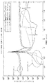
この点について、図8は、圧電層46がY+42度の配向を有するLT膜である、SAWデバイス44の実装についてのシミュレーション結果を示し、石英キャリア基板48は、Y+36度の配向を有する石英から形成され、SAWの伝搬は、石英キャリア基板48の水晶振動子のx軸沿いにあり(すなわち、X伝搬があり)、そこで石英キャリア基板48の水晶振動子のx軸は、LTのx軸とアライメントを取る。これらの結果は、石英キャリア基板48内のバルクカットオフ周波数がSAWデバイス44の共振周波数より低いことを示す。これは、音響エネルギーがバルク内に放射されることが可能であり、伝搬損失及び低い品質係数をもたらすことを意味する。したがって、これは、望ましくない配向である。
In this regard, FIG. 8 shows simulation results for mounting the
同様に、図9は、圧電層46がY+42度の配向を有するLT膜であり、石英キャリア基板48がY+36度の配向を有するが、石英キャリア基板48の水晶振動子のx軸から90度においてSAWの伝搬を有する、石英から形成される、SAWデバイス44の実装についてのシミュレーション結果を示す。これは、石英上のいわゆる横波型弾性表面波(STW)デバイスについての配向である。図示されるように、バルクカットオフ周波数は、メインモードがバルク内へ漏洩させ、その品質係数を低下させる、SAWデバイス44の共振周波数に近い周波数にある。したがって、これも、望ましくない配向である。
Similarly, FIG. 9 shows an LT film in which the piezoelectric layer 46 has an orientation of Y + 42 degrees and the
この問題は、石英のこれらの配向についての石英キャリア基板48におけるバルクモードが遅すぎることである。カットオフ周波数を上回る、多くのエネルギーは、バルク内に損失する。pが金属トランスデューサ52の電極周期である場合に、カットオフ周波数は、Vs/2pであり、そこでVsは、SAWの伝搬方向についての石英キャリア基板48における速度である。石英における速度は、低すぎることが多い。
The problem is that the bulk mode in the
図10から図12は、XY、XZ、及びYZ平面における石英についてのBAWスローネス曲線を示す。ほとんどの配向について、最も低い速度が3300メートル/秒(m/s)から4000m/sの間にあることを示す。これらの速度は、LTにおける速度と比較して低すぎる(すなわち、対応するカットオフ周波数は共振周波数を上回るほど高くはない)。最も高いせん断速度を有する配向は、約4660m/sの速度を有する、Z配向である。共振周波数(この実施例について、2マイクロメートル(μm)周期に対して1ギガヘルツ(GHz)と仮定される)より高い10%を超えるカットオフ周波数を有するため、石英における速度は、少なくとも4400m/sである、またはスローネスは、2.273 10−4秒/メートル(s/m)未満である。XZ平面におけるこの条件は、z軸(または−z軸)周囲の±8度、及びYZ平面における±10度の角度範囲についてのみである。世界的に、これは、キャリア基板48が水晶振動子のz軸に関して10度より小さい角度をなす伝搬方向を有する石英の基板でなければならないことを意味する。このようなものとして、上記に言及されるように、いくつかの実施形態において、金属トランスデューサ52の伝搬方向は、石英キャリア基板48の水晶振動子のz軸または−z軸に関して10度より小さい角度を形成する。
10 to 12 show BAW slowness curves for quartz in the XY, XZ, and YZ planes. For most orientations, the lowest velocities are between 3300 m / s (m / s) and 4000 m / s. These velocities are too low compared to the velocities in LT (ie, the corresponding cutoff frequencies are not high enough to exceed the resonant frequencies). The orientation with the highest shear rate is the Z orientation, which has a rate of about 4660 m / s. The velocity in quartz is at least 4400 m / s because it has a cutoff frequency greater than 10%, which is higher than the resonance frequency (assumed to be 1 gigahertz (GHz) for a 2 micrometer (μm) period for this example). Or the slowness is less than 2.273 10-4 seconds / meter (s / m). This condition in the XZ plane is only for an angular range of ± 8 degrees around the z-axis (or -z-axis) and ± 10 degrees in the YZ plane. Globally, this means that the
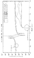
図13は、圧電層46がY+42度の配向、石英Yカットから作製される石英キャリア基板48上のX伝搬、及び石英キャリア基板48の水晶振動子のz軸沿いのSAWの伝搬(すなわち、Z伝搬)を有するLT膜である、SAWデバイス44(SAW共振子として)の実装についてのシミュレーション結果を示す。換言すれば、結晶学的なLTのx軸は、結晶学的な石英のz軸とアライメントを取る。結晶学的な石英のy軸は、石英の平面に垂直であり、LTについてのY+42軸は、この表面に垂直である。スローネス曲線により予測されるように、バルクカットオフ周波数は、共振周波数を上回り十分に離れており、良好なガイドを有する(及び同一の基板上にあるが異なる周波数を有するこの共振子及び他のものを使用して、フィルタ(たとえば、ラダー型フィルタ)を作製する場合に、フィルタの帯域における放射損失を有さない)。また、非常になめらかな応答は、スプリアスモードなしで得られる。
FIG. 13 shows the orientation of the piezoelectric layer 46 at Y + 42 degrees, the X propagation on the
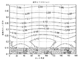
上述される最適化に加えて、いくつかの実施形態において、石英キャリア基板48のために使用される石英のカット角度も、たとえば、圧電結合及び/またはTCFなどの、SAWデバイス44の1つ以上の性能パラメータを最適化するように選択される。この点について、図14から図16は、圧電層46がYXI42(すなわち、Y+42)の配向を有するLT膜である、SAWデバイス44の1つの例示的な実施態様についてのシミュレーション結果を示し、そこでキャリア基板48は、石英キャリア基板48についてのカット角度シータ(グラフ内のx軸)、及び波長内のLTの厚さ(グラフ内のy軸)の関数として、配向XZI tetaを有する石英(すなわち、z軸沿いの伝搬、及びz軸沿いに回転する平面を有する石英、そこで0はX配向に対応し、90はY配向に対応する)から作製される。図14において、最高の圧電結合がZ伝搬に関してXまたはYカット石英のキャリア基板に対応する、0または90度に近い角度シータについて得られることを明確に理解することが可能である。図15及び図16において、TCFについての最高の結果が40度(たとえば、30度から55度の範囲)、または140度(たとえば、130度から155度の範囲)に近い角度シータについて得られることを明確に理解することが可能である。
In addition to the optimizations described above, in some embodiments, the quartz cut angle used for the
図17Aから図17Gは、本開示のいくつかの実施形態に従い、図7のSAWデバイス44を製造するプロセスを示す。図17Aに示されるように、プロセスは、石英キャリア基板48により開始する。図17Bに示されるように、1層以上の誘電体層50(及び/または他のタイプの追加の層)は、石英キャリア基板48の表面上に形成される(たとえば、成膜する、または結合される)。また、誘電体層(複数可)50は、任意選択である。圧電材料54は、図17Cに示されるように、石英キャリア基板48に対向する誘電体層(複数可)50の表面上に(または誘電体層(複数可)50が存在しない場合に石英キャリア基板48の表面上に)結合される。図17Dに示されるように、圧電材料54を研削し、またはその他の方法で処理し、所望の厚さ(t圧電)を有する圧電層46を形成する。結果として生じる構造を図17Eに示す。つぎに金属トランスデューサ52は、図17Fに示されるように、誘電体層(複数可)50(存在する場合に)及び石英キャリア基板48に対向する圧電層46の表面上に(たとえば、表面上に直接に)形成される。任意選択で、1層以上の誘電体層53は、図17Gに示されるように、金属トランスデューサ52の表面、及び圧電層46の露出面上に形成される(たとえば、成膜する)。
17A-17G show the process of manufacturing the
図18Aから図18Hは、本開示のいくつかの他の実施形態に従い、図7のSAWデバイス44を製造するプロセスを示す。図18Aに示されるように、プロセスは、石英キャリア基板48により開始する。図18Bに示されるように、1層以上の誘電体層50(及び/または他のタイプの追加の層)は、石英キャリア基板48の表面上に形成される(たとえば、成膜する、または結合される)。また、誘電体層(複数可)50は、任意選択である。図18Cに示されるように、圧電材料54の表面内へのイオン注入を使用して、圧電層46の所望の厚さ(t圧電)を画定する、所望の、または制御された深さにおいて圧電材料54内に損傷した層54Aを作製する。圧電材料54は、図18Dに示されるように、石英キャリア基板48に対向する誘電体層(複数可)50の表面上に(または誘電体層(複数可)50が存在しない場合に石英キャリア基板48の表面上に)結合される。図18E及び図18Fに示されるように、損傷した層54Aより上の圧電材料54の部分を除去することにより、所望の厚さ(t圧電)を有する圧電層46を形成する。特に、圧電層46の表面を好ましくは研磨し、圧電層46の表面上に残るいかなる欠陥も取り除く。結果として生じる構造は、図18Fに示される。つぎに金属トランスデューサ52は、図18Gに示されるように、誘電体層(複数可)50(存在する場合に)及び石英キャリア基板48に対向する圧電層46の表面上に(たとえば、表面上に直接に)形成される。任意選択で、つぎに1層以上の誘電体層53は、図18Hに示されるように、金属トランスデューサ52の表面、及び下層の露出面上に形成される(たとえば、成膜する)。
18A-18H show the process of manufacturing the
本開示は、限定されないが、つぎのものを提供する。
キャリア基板上に結合される、または成膜する圧電層を備える基板上に少なくとも1つの交差指電極を含む音波共振子であって、そこで前記キャリア基板は石英であり、前記圧電層厚はたとえば、4倍の前記トランスデューサ電極周期より小さく、他の実施形態において、2倍の前記トランスデューサ電極周期より小さく、
○そこで前記圧電膜はYからY+60度の間の配向を有するタンタル酸リチウム(LiTaO3)から作製され、
○そこで前記圧電膜はY−20度からY+60度の間の配向を有するニオブ酸リチウム(LiNbO3)から作製され、
○そこで前記トランスデューサ電極周期より薄い厚さを有する追加の層は前記キャリア基板と前記圧電層との間に配置され、
■そこで前記追加の層のうちの少なくとも1層は酸化ケイ素から作製され、
○そこで前記圧電層は薄膜を得るために、前記キャリア基板上に圧電材料のウェハを結合することにより、及び前記圧電材料のウェハを研削することにより作製され、
○そこで前記圧電層は所与の深さにおいて前記ウェハ内の欠陥を生じるために圧電材料のウェハ内にイオンを注入することにより、このウェハを前記キャリア基板に結合することにより、前記圧電材料を前記欠陥の前記位置において分割することにより、及び前記圧電材料を研磨することにより作製され、
○そこで前記キャリアウェハは、石英から作製され、そこで前記トランスデューサの前記伝搬方向は前記水晶振動子の前記軸zまたは−zに関して10度より小さい角度を形成し、
■そこで前記圧電層はYからY+60度の間の配向、及びX沿いの伝搬を有するLiTaO3から作製され、
●そこで前記圧電層の前記厚さは前記トランスデューサの前記電極周期の60%未満であり、
○そこで前記キャリア基板は前記石英の前記xまたはy軸沿いにその法線配向を有する石英であり、
○そこで前記キャリア基板は前記石英の前記x軸に関して30度から55度の間の角度を形成するその法線を有する石英であり、
■そこで前記LiTaO3層厚は前記電極周期の20%から40%の間にあり、
■そこで前記LiTaO3層厚は前記電極周期の30%から50%の間にあり、
○そこで少なくとも1つの共振子は結合型共振子フィルタ内に実装され、
■そこで前記結合型共振子フィルタは2つのグレーティング間に配置される少なくとも2つのトランスデューサを含み、
●そこで少なくとも1つの共振子素子はラダー型フィルタに組み込まれ、
○そこで前記結合型共振子フィルタの前記カスケードを使用するフィルタ、及び少なくとも1つの共振子は直列で、または並列で接続され、
●そこで少なくとも1つのフィルタはデュプレクサ内に組み込まれる、
前記音波共振子。
The present disclosure provides, but is not limited to,:
A sonic resonator comprising at least one intersecting finger electrode on a substrate comprising a piezoelectric layer coupled or deposited on a carrier substrate, wherein the carrier substrate is quartz and the piezoelectric layer thickness is, for example, 4 times smaller than the transducer electrode period, and in other embodiments, 2 times smaller than the transducer electrode period.
○ Therefore, the piezoelectric film is made of lithium tantalate (LiTaO 3 ) having an orientation between Y and Y + 60 degrees.
○ Therefore, the piezoelectric film is made of lithium niobate (LiNbO 3 ) having an orientation between Y-20 degrees and Y + 60 degrees.
○ Therefore, an additional layer having a thickness thinner than the transducer electrode period is arranged between the carrier substrate and the piezoelectric layer.
■ There, at least one of the additional layers is made from silicon oxide.
○ Therefore, the piezoelectric layer is produced by bonding a wafer of a piezoelectric material on the carrier substrate and by grinding the wafer of the piezoelectric material in order to obtain a thin film.
○ Therefore, the piezoelectric layer is formed by injecting ions into the wafer of the piezoelectric material in order to cause defects in the wafer at a given depth, thereby binding the wafer to the carrier substrate, thereby forming the piezoelectric material. It is made by dividing at the position of the defect and by polishing the piezoelectric material.
There, the carrier wafer is made of quartz, where the propagation direction of the transducer forms an angle less than 10 degrees with respect to the axis z or −z of the crystal oscillator.
(3) The piezoelectric layer is then made from LiTaO 3, which has an orientation between Y and Y + 60 degrees and propagation along X.
● Therefore, the thickness of the piezoelectric layer is less than 60% of the electrode period of the transducer.
○ Therefore, the carrier substrate is quartz having its normal orientation along the x or y axis of the quartz.
○ Therefore, the carrier substrate is quartz having a normal line forming an angle between 30 degrees and 55 degrees with respect to the x-axis of the quartz.
■ Therefore, the LiTaO 3 layer thickness is between 20% and 40% of the electrode cycle.
■ Therefore, the LiTaO 3 layer thickness is between 30% and 50% of the electrode cycle.
○ There, at least one resonator is mounted in the coupled resonator filter,
■ Therefore, the coupled resonator filter includes at least two transducers arranged between the two gratings.
● Therefore, at least one resonator element is incorporated in the ladder type filter.
○ Therefore, a filter using the cascade of the coupled resonator filter and at least one resonator are connected in series or in parallel.
● There, at least one filter is built into the duplexer,
The sound wave resonator.
当業者は、本開示の好ましい実施形態への改良及び変更を認識するであろう。すべてのこれらのような改良及び変更は、本明細書に開示される概念の範囲、及び以下の特許請求の範囲内にあると考察される。 Those skilled in the art will recognize improvements and changes to the preferred embodiments of the present disclosure. All such improvements and changes are considered to be within the scope of the concepts disclosed herein and within the claims below.
Claims (21)
前記石英キャリア基板の表面上の圧電層であって、前記圧電層は、0度から60度の間の結晶y軸の回転角を有し、前記圧電層の結晶x軸に沿った伝搬方向を有するタンタル酸リチウムから形成される、圧電層、及び
前記石英キャリア基板に対向する前記圧電層の表面上に少なくとも1つの交差指電極、
を備え、前記少なくとも1つの交差指電極の弾性表面波の伝搬方向は、前記石英キャリア基板の結晶z軸または−z軸に関して10度未満の角度を形成する、弾性表面波(SAW)デバイス。 Quartz carrier substrate,
A piezoelectric layer on the surface of the quartz carrier substrate, the piezoelectric layer has a rotation angle of the crystal y-axis between 0 degrees and 60 degrees, and has a propagation direction along the crystal x-axis of the piezoelectric layer. A piezoelectric layer formed from lithium tantalate, and at least one cross finger electrode on the surface of the piezoelectric layer facing the quartz carrier substrate.
A surface acoustic wave (SAW) device comprising, wherein the surface acoustic wave propagation direction of the at least one crossed finger electrode forms an angle of less than 10 degrees with respect to the crystal z-axis or −z axis of the quartz carrier substrate.
前記石英キャリア基板の表面上の圧電層であって、前記圧電層は、0度から60度の間の結晶のy軸の回転角を有し、前記圧電層の結晶のx軸沿いの伝搬方向を有するタンタル酸リチウムから形成される、圧電層、及び
前記石英キャリア基板に対向する前記圧電層の表面上の少なくとも1つの交差指電極、
を含む、弾性表面波(SAW)共振子、
を備え、前記少なくとも1つの交差指電極の弾性表面波の伝搬方向は、前記石英キャリア基板の結晶z軸または−z軸に関して10度未満の角度を形成する、フィルタリング回路。 Quartz carrier substrate,
A piezoelectric layer on the surface of the quartz carrier substrate, the piezoelectric layer has a y-axis rotation angle of the crystal between 0 and 60 degrees, and the propagation direction of the crystal of the piezoelectric layer along the x-axis. A piezoelectric layer formed of lithium tantalate, and at least one cross finger electrode on the surface of the piezoelectric layer facing the quartz carrier substrate.
Surface Acoustic Wave (SAW) resonators, including
A filtering circuit comprising, wherein the surface acoustic wave propagation direction of the at least one crossed finger electrode forms an angle of less than 10 degrees with respect to the crystal z-axis or −z axis of the quartz carrier substrate.
前記石英キャリア基板の表面上に圧電層を提供し、前記圧電層は、0度から60度の間の結晶のy軸の回転角を有し、前記圧電層の結晶のx軸沿いの伝搬方向を有するタンタル酸リチウムから形成される、圧電層を提供し、
前記石英キャリア基板に対向する前記圧電層の表面上に少なくとも1つの交差指電極を提供する、
ことを備え、前記少なくとも1つの交差指電極の弾性表面波の伝搬方向は、前記石英キャリア基板の結晶z軸または−z軸に関して10度未満の角度を形成する、弾性表面波(SAW)デバイスを製造する方法。 Providing a quartz carrier substrate,
A piezoelectric layer is provided on the surface of the quartz carrier substrate, and the piezoelectric layer has a rotation angle of the y-axis of the crystal between 0 and 60 degrees, and the propagation direction of the crystal of the piezoelectric layer along the x-axis. Provides a piezoelectric layer, formed from lithium tantalate with
At least one cross-finger electrode is provided on the surface of the piezoelectric layer facing the quartz carrier substrate.
A surface acoustic wave (SAW) device, wherein the surface acoustic wave propagation direction of the at least one crossed finger electrode forms an angle of less than 10 degrees with respect to the crystal z-axis or −z axis of the quartz carrier substrate. How to manufacture.
前記石英キャリア基板の表面上の圧電層であって、前前記圧電層は、0度から60度の間の結晶のy軸の回転角を有し、前記圧電層の結晶のx軸沿いの伝搬方向を有するタンタル酸リチウムから形成される、圧電層、及び
前記石英キャリア基板に対向する前記圧電層の表面上の少なくとも1つの交差指電極、
を備え、前記圧電層の結晶x軸は、前記石英キャリア基板の結晶z軸とアライメントを取る、弾性表面波(SAW)デバイス。 Quartz carrier substrate,
A piezoelectric layer on the surface of the quartz carrier substrate, the front piezoelectric layer having a y-axis rotation angle of the crystal between 0 and 60 degrees, and propagating along the x-axis of the crystal of the piezoelectric layer. A piezoelectric layer formed of directional lithium tantalate, and at least one intersecting finger electrode on the surface of the piezoelectric layer facing the quartz carrier substrate.
A surface acoustic wave (SAW) device, wherein the crystal x-axis of the piezoelectric layer is aligned with the crystal z-axis of the quartz carrier substrate.
Priority Applications (1)
| Application Number | Priority Date | Filing Date | Title |
|---|---|---|---|
| JP2021073990A JP7317068B2 (en) | 2016-01-28 | 2021-04-26 | Surface acoustic wave device including piezoelectric layer on quartz substrate and manufacturing method thereof |
Applications Claiming Priority (5)
| Application Number | Priority Date | Filing Date | Title |
|---|---|---|---|
| US201662288018P | 2016-01-28 | 2016-01-28 | |
| US62/288,018 | 2016-01-28 | ||
| US15/086,895 | 2016-03-31 | ||
| US15/086,895 US10084427B2 (en) | 2016-01-28 | 2016-03-31 | Surface acoustic wave device having a piezoelectric layer on a quartz substrate and methods of manufacturing thereof |
| PCT/US2017/014806 WO2017132183A1 (en) | 2016-01-28 | 2017-01-25 | Surface acoustic wave device having a piezoelectric layer on a quartz substrate and methods of manufacturing thereof |
Related Child Applications (1)
| Application Number | Title | Priority Date | Filing Date |
|---|---|---|---|
| JP2021073990A Division JP7317068B2 (en) | 2016-01-28 | 2021-04-26 | Surface acoustic wave device including piezoelectric layer on quartz substrate and manufacturing method thereof |
Publications (3)
| Publication Number | Publication Date |
|---|---|
| JP2019507546A JP2019507546A (en) | 2019-03-14 |
| JP2019507546A5 JP2019507546A5 (en) | 2020-01-30 |
| JP6877447B2 true JP6877447B2 (en) | 2021-05-26 |
Family
ID=59387138
Family Applications (2)
| Application Number | Title | Priority Date | Filing Date |
|---|---|---|---|
| JP2018539290A Active JP6877447B2 (en) | 2016-01-28 | 2017-01-25 | Surface acoustic wave device including a piezoelectric layer on a quartz substrate and its manufacturing method |
| JP2021073990A Active JP7317068B2 (en) | 2016-01-28 | 2021-04-26 | Surface acoustic wave device including piezoelectric layer on quartz substrate and manufacturing method thereof |
Family Applications After (1)
| Application Number | Title | Priority Date | Filing Date |
|---|---|---|---|
| JP2021073990A Active JP7317068B2 (en) | 2016-01-28 | 2021-04-26 | Surface acoustic wave device including piezoelectric layer on quartz substrate and manufacturing method thereof |
Country Status (3)
| Country | Link |
|---|---|
| US (2) | US10084427B2 (en) |
| JP (2) | JP6877447B2 (en) |
| WO (1) | WO2017132183A1 (en) |
Families Citing this family (133)
| Publication number | Priority date | Publication date | Assignee | Title |
|---|---|---|---|---|
| US8735219B2 (en) | 2012-08-30 | 2014-05-27 | Ziptronix, Inc. | Heterogeneous annealing method and device |
| US10574203B2 (en) | 2015-07-28 | 2020-02-25 | Qorvo Us, Inc. | Bonded wafers and surface acoustic wave devices using same |
| US10812038B2 (en) * | 2015-08-25 | 2020-10-20 | Avago Technologies International Sales Pte. Limited | Acoustic wave resonator |
| US10128814B2 (en) | 2016-01-28 | 2018-11-13 | Qorvo Us, Inc. | Guided surface acoustic wave device providing spurious mode rejection |
| US10084427B2 (en) | 2016-01-28 | 2018-09-25 | Qorvo Us, Inc. | Surface acoustic wave device having a piezoelectric layer on a quartz substrate and methods of manufacturing thereof |
| US11095266B2 (en) | 2016-10-07 | 2021-08-17 | Qorvo Us, Inc. | Slanted apodization for acoustic wave devices |
| US10924086B2 (en) | 2016-10-14 | 2021-02-16 | Qorvo Us, Inc. | Surface acoustic wave (SAW) device with antireflective structure |
| US10848121B2 (en) | 2016-10-14 | 2020-11-24 | Qorvo Us, Inc. | Guided SAW device |
| US10924085B2 (en) | 2016-10-17 | 2021-02-16 | Qorvo Us, Inc. | Guided acoustic wave device |
| TWI780103B (en) * | 2017-05-02 | 2022-10-11 | 日商日本碍子股份有限公司 | Elastic wave element and method of manufacturing the same |
| JP6963423B2 (en) | 2017-06-14 | 2021-11-10 | 株式会社日本製鋼所 | Manufacturing method of bonded substrate, surface acoustic wave element and bonded substrate |
| JP2019036963A (en) * | 2017-08-18 | 2019-03-07 | スカイワークス ソリューションズ, インコーポレイテッドSkyworks Solutions, Inc. | Filter with surface acoustic wave device for carrier aggregation system |
| US11206007B2 (en) | 2017-10-23 | 2021-12-21 | Qorvo Us, Inc. | Quartz orientation for guided SAW devices |
| JP7170402B2 (en) * | 2018-02-16 | 2022-11-14 | 株式会社日本製鋼所 | Bonded substrate, surface acoustic wave element, surface acoustic wave element device, and bonding substrate manufacturing method |
| US20220116015A1 (en) | 2018-06-15 | 2022-04-14 | Resonant Inc. | Transversely-excited film bulk acoustic resonator with optimized electrode thickness, mark, and pitch |
| US11936358B2 (en) | 2020-11-11 | 2024-03-19 | Murata Manufacturing Co., Ltd. | Transversely-excited film bulk acoustic resonator with low thermal impedance |
| US11323089B2 (en) | 2018-06-15 | 2022-05-03 | Resonant Inc. | Filter using piezoelectric film bonded to high resistivity silicon substrate with trap-rich layer |
| US11509279B2 (en) | 2020-07-18 | 2022-11-22 | Resonant Inc. | Acoustic resonators and filters with reduced temperature coefficient of frequency |
| US10790802B2 (en) | 2018-06-15 | 2020-09-29 | Resonant Inc. | Transversely excited film bulk acoustic resonator using rotated Y-X cut lithium niobate |
| US10911023B2 (en) | 2018-06-15 | 2021-02-02 | Resonant Inc. | Transversely-excited film bulk acoustic resonator with etch-stop layer |
| US10601392B2 (en) | 2018-06-15 | 2020-03-24 | Resonant Inc. | Solidly-mounted transversely-excited film bulk acoustic resonator |
| US10637438B2 (en) | 2018-06-15 | 2020-04-28 | Resonant Inc. | Transversely-excited film bulk acoustic resonators for high power applications |
| US11146232B2 (en) | 2018-06-15 | 2021-10-12 | Resonant Inc. | Transversely-excited film bulk acoustic resonator with reduced spurious modes |
| US10756697B2 (en) | 2018-06-15 | 2020-08-25 | Resonant Inc. | Transversely-excited film bulk acoustic resonator |
| US12040779B2 (en) | 2020-04-20 | 2024-07-16 | Murata Manufacturing Co., Ltd. | Small transversely-excited film bulk acoustic resonators with enhanced Q-factor |
| US11323090B2 (en) | 2018-06-15 | 2022-05-03 | Resonant Inc. | Transversely-excited film bulk acoustic resonator using Y-X-cut lithium niobate for high power applications |
| US11323096B2 (en) | 2018-06-15 | 2022-05-03 | Resonant Inc. | Transversely-excited film bulk acoustic resonator with periodic etched holes |
| US12088281B2 (en) | 2021-02-03 | 2024-09-10 | Murata Manufacturing Co., Ltd. | Transversely-excited film bulk acoustic resonator with multi-mark interdigital transducer |
| US11996827B2 (en) | 2018-06-15 | 2024-05-28 | Murata Manufacturing Co., Ltd. | Transversely-excited film bulk acoustic resonator with periodic etched holes |
| US11206009B2 (en) | 2019-08-28 | 2021-12-21 | Resonant Inc. | Transversely-excited film bulk acoustic resonator with interdigital transducer with varied mark and pitch |
| US11929731B2 (en) | 2018-02-18 | 2024-03-12 | Murata Manufacturing Co., Ltd. | Transversely-excited film bulk acoustic resonator with optimized electrode mark, and pitch |
| JP7080671B2 (en) | 2018-02-27 | 2022-06-06 | NDK SAW devices株式会社 | Surface acoustic wave device |
| NO345072B1 (en) * | 2018-03-08 | 2020-09-21 | Kongsberg Defence & Aerospace As | Correction Unit for RF filter |
| FR3079667B1 (en) * | 2018-03-28 | 2020-03-27 | Frec'n'sys | SURFACE ACOUSTIC WAVE DEVICE ON COMPOSITE SUBSTRATE |
| DE102018108605A1 (en) * | 2018-04-11 | 2019-10-17 | RF360 Europe GmbH | SAW resonator with improved power and heat resistance and SAW resonator comprising RF filter |
| DE102018108961A1 (en) * | 2018-04-16 | 2019-10-17 | RF360 Europe GmbH | TF-SAW resonator with improved quality factor, RF filter and method for producing a TF-SAW resonator |
| US11050406B2 (en) | 2018-05-21 | 2021-06-29 | Skyworks Solutions, Inc. | Multi-layer piezoelectric substrate with heat dissipation |
| US11916539B2 (en) | 2020-02-28 | 2024-02-27 | Murata Manufacturing Co., Ltd. | Split-ladder band N77 filter using transversely-excited film bulk acoustic resonators |
| US11901878B2 (en) | 2018-06-15 | 2024-02-13 | Murata Manufacturing Co., Ltd. | Transversely-excited film bulk acoustic resonators with two-layer electrodes with a wider top layer |
| US11329628B2 (en) | 2020-06-17 | 2022-05-10 | Resonant Inc. | Filter using lithium niobate and lithium tantalate transversely-excited film bulk acoustic resonators |
| US10985728B2 (en) | 2018-06-15 | 2021-04-20 | Resonant Inc. | Transversely-excited film bulk acoustic resonator and filter with a uniform-thickness dielectric overlayer |
| US11909381B2 (en) | 2018-06-15 | 2024-02-20 | Murata Manufacturing Co., Ltd. | Transversely-excited film bulk acoustic resonators with two-layer electrodes having a narrower top layer |
| US11349452B2 (en) | 2018-06-15 | 2022-05-31 | Resonant Inc. | Transversely-excited film bulk acoustic filters with symmetric layout |
| US11876498B2 (en) | 2018-06-15 | 2024-01-16 | Murata Manufacturing Co., Ltd. | Transversely-excited film bulk acoustic resonator with multiple diaphragm thicknesses and fabrication method |
| US12119808B2 (en) | 2018-06-15 | 2024-10-15 | Murata Manufacturing Co., Ltd. | Transversely-excited film bulk acoustic resonator package |
| US10992284B2 (en) | 2018-06-15 | 2021-04-27 | Resonant Inc. | Filter using transversely-excited film bulk acoustic resonators with multiple frequency setting layers |
| US11146238B2 (en) | 2018-06-15 | 2021-10-12 | Resonant Inc. | Film bulk acoustic resonator fabrication method |
| US11870423B2 (en) | 2018-06-15 | 2024-01-09 | Murata Manufacturing Co., Ltd. | Wide bandwidth temperature-compensated transversely-excited film bulk acoustic resonator |
| US10917072B2 (en) | 2019-06-24 | 2021-02-09 | Resonant Inc. | Split ladder acoustic wave filters |
| US11996825B2 (en) | 2020-06-17 | 2024-05-28 | Murata Manufacturing Co., Ltd. | Filter using lithium niobate and rotated lithium tantalate transversely-excited film bulk acoustic resonators |
| US12113512B2 (en) | 2021-03-29 | 2024-10-08 | Murata Manufacturing Co., Ltd. | Layout of XBARs with multiple sub-resonators in parallel |
| US11201601B2 (en) | 2018-06-15 | 2021-12-14 | Resonant Inc. | Transversely-excited film bulk acoustic resonator with multiple diaphragm thicknesses and fabrication method |
| US11728785B2 (en) | 2018-06-15 | 2023-08-15 | Murata Manufacturing Co., Ltd. | Transversely-excited film bulk acoustic resonator using pre-formed cavities |
| US12040781B2 (en) | 2018-06-15 | 2024-07-16 | Murata Manufacturing Co., Ltd. | Transversely-excited film bulk acoustic resonator package |
| US11264966B2 (en) | 2018-06-15 | 2022-03-01 | Resonant Inc. | Solidly-mounted transversely-excited film bulk acoustic resonator with diamond layers in Bragg reflector stack |
| US11374549B2 (en) | 2018-06-15 | 2022-06-28 | Resonant Inc. | Filter using transversely-excited film bulk acoustic resonators with divided frequency-setting dielectric layers |
| US11949402B2 (en) | 2020-08-31 | 2024-04-02 | Murata Manufacturing Co., Ltd. | Resonators with different membrane thicknesses on the same die |
| US12021496B2 (en) | 2020-08-31 | 2024-06-25 | Murata Manufacturing Co., Ltd. | Resonators with different membrane thicknesses on the same die |
| US11996822B2 (en) | 2018-06-15 | 2024-05-28 | Murata Manufacturing Co., Ltd. | Wide bandwidth time division duplex transceiver |
| US10797675B2 (en) | 2018-06-15 | 2020-10-06 | Resonant Inc. | Transversely excited film bulk acoustic resonator using rotated z-cut lithium niobate |
| US10868513B2 (en) | 2018-06-15 | 2020-12-15 | Resonant Inc. | Transversely-excited film bulk acoustic filters with symmetric layout |
| US11349450B2 (en) | 2018-06-15 | 2022-05-31 | Resonant Inc. | Symmetric transversely-excited film bulk acoustic resonators with reduced spurious modes |
| US11323095B2 (en) | 2018-06-15 | 2022-05-03 | Resonant Inc. | Rotation in XY plane to suppress spurious modes in XBAR devices |
| US11967945B2 (en) | 2018-06-15 | 2024-04-23 | Murata Manufacturing Co., Ltd. | Transversly-excited film bulk acoustic resonators and filters |
| US12119805B2 (en) | 2018-06-15 | 2024-10-15 | Murata Manufacturing Co., Ltd. | Substrate processing and membrane release of transversely-excited film bulk acoustic resonator using a sacrificial tub |
| US10998877B2 (en) | 2018-06-15 | 2021-05-04 | Resonant Inc. | Film bulk acoustic resonator fabrication method with frequency trimming based on electric measurements prior to cavity etch |
| US12009798B2 (en) | 2018-06-15 | 2024-06-11 | Murata Manufacturing Co., Ltd. | Transversely-excited film bulk acoustic resonators with electrodes having irregular hexagon cross-sectional shapes |
| US10992283B2 (en) | 2018-06-15 | 2021-04-27 | Resonant Inc. | High power transversely-excited film bulk acoustic resonators on rotated Z-cut lithium niobate |
| US11171629B2 (en) | 2018-06-15 | 2021-11-09 | Resonant Inc. | Transversely-excited film bulk acoustic resonator using pre-formed cavities |
| US12081187B2 (en) * | 2018-06-15 | 2024-09-03 | Murata Manufacturing Co., Ltd. | Transversely-excited film bulk acoustic resonator |
| US10826462B2 (en) | 2018-06-15 | 2020-11-03 | Resonant Inc. | Transversely-excited film bulk acoustic resonators with molybdenum conductors |
| US11228296B2 (en) | 2018-06-15 | 2022-01-18 | Resonant Inc. | Transversely-excited film bulk acoustic resonator with a cavity having a curved perimeter |
| US11323091B2 (en) | 2018-06-15 | 2022-05-03 | Resonant Inc. | Transversely-excited film bulk acoustic resonator with diaphragm support pedestals |
| US10998882B2 (en) | 2018-06-15 | 2021-05-04 | Resonant Inc. | XBAR resonators with non-rectangular diaphragms |
| US12095446B2 (en) | 2018-06-15 | 2024-09-17 | Murata Manufacturing Co., Ltd. | Transversely-excited film bulk acoustic resonator with optimized electrode thickness, mark, and pitch |
| US11888463B2 (en) | 2018-06-15 | 2024-01-30 | Murata Manufacturing Co., Ltd. | Multi-port filter using transversely-excited film bulk acoustic resonators |
| CN112272920B (en) * | 2018-06-22 | 2021-11-16 | 日本碍子株式会社 | Bonded body and elastic wave element |
| WO2020010056A1 (en) | 2018-07-03 | 2020-01-09 | Invensas Bonding Technologies, Inc. | Techniques for joining dissimilar materials in microelectronics |
| JP7231368B2 (en) * | 2018-09-26 | 2023-03-01 | 太陽誘電株式会社 | elastic wave device |
| JP2022512700A (en) * | 2018-10-16 | 2022-02-07 | 国立大学法人東北大学 | Elastic wave device |
| CN118523746A (en) * | 2018-10-31 | 2024-08-20 | 株式会社村田制作所 | Solid-state assembly type transversely-excited film bulk acoustic resonator |
| JP2020145567A (en) * | 2019-03-06 | 2020-09-10 | 株式会社村田製作所 | Acoustic wave device |
| WO2020186261A1 (en) | 2019-03-14 | 2020-09-17 | Resonant Inc. | Transversely-excited film bulk acoustic resonator with half-lambda dielectric layer |
| US11901873B2 (en) | 2019-03-14 | 2024-02-13 | Murata Manufacturing Co., Ltd. | Transversely-excited film bulk acoustic resonator with partial BRAGG reflectors |
| CN118316415A (en) | 2019-04-05 | 2024-07-09 | 株式会社村田制作所 | Transverse excited film bulk acoustic resonator package and method |
| WO2020250490A1 (en) | 2019-06-11 | 2020-12-17 | 日本碍子株式会社 | Composite substrate, elastic wave element, and production method for composite substrate |
| JP6776484B1 (en) | 2019-06-11 | 2020-10-28 | 日本碍子株式会社 | Composite substrate and elastic wave element |
| WO2020250491A1 (en) | 2019-06-11 | 2020-12-17 | 日本碍子株式会社 | Composite substrate, elastic wave element, and production method for composite substrate |
| EP3985869A4 (en) | 2019-06-11 | 2022-08-10 | NGK Insulators, Ltd. | Composite substrate, elastic wave element, and production method for composite substrate |
| US10911021B2 (en) | 2019-06-27 | 2021-02-02 | Resonant Inc. | Transversely-excited film bulk acoustic resonator with lateral etch stop |
| US12034423B2 (en) | 2019-06-27 | 2024-07-09 | Murata Manufacturing Co., Ltd | XBAR frontside etch process using polysilicon sacrificial layer |
| JPWO2021002047A1 (en) * | 2019-07-03 | 2021-09-13 | 日本碍子株式会社 | Bonds and seismic elements |
| KR20220011693A (en) * | 2019-07-05 | 2022-01-28 | 가부시키가이샤 무라타 세이사쿠쇼 | Acoustic wave devices, high-frequency front-end circuits and communication devices |
| JP7510416B2 (en) * | 2019-07-05 | 2024-07-03 | 株式会社村田製作所 | Acoustic wave device, high frequency front-end circuit and communication device |
| US10862454B1 (en) | 2019-07-18 | 2020-12-08 | Resonant Inc. | Film bulk acoustic resonators in thin LN-LT layers |
| US11329625B2 (en) | 2019-07-18 | 2022-05-10 | Resonant Inc. | Film bulk acoustic sensors using thin LN-LT layer |
| JP7334786B2 (en) * | 2019-09-27 | 2023-08-29 | 株式会社村田製作所 | elastic wave filter |
| US20210111688A1 (en) * | 2019-10-10 | 2021-04-15 | Skyworks Solutions, Inc. | Surface acoustic wave device with multi-layer piezoelectric substrate |
| US11804822B2 (en) | 2019-10-23 | 2023-10-31 | Skyworks Solutions, Inc. | Surface acoustic wave resonator with reduced frequency shift |
| DE112020005340T5 (en) * | 2019-11-27 | 2022-08-18 | Skyworks Solutions, Inc. | ENERGY CONTAINMENT IN ACOUSTIC WAVE DEVICES |
| JP2021118366A (en) * | 2020-01-22 | 2021-08-10 | 株式会社日本製鋼所 | Surface acoustic wave filter and manufacturing method of the same |
| US20210273629A1 (en) | 2020-02-28 | 2021-09-02 | Resonant Inc. | Transversely-excited film bulk acoustic resonator with multi-pitch interdigital transducer |
| CN115943489A (en) | 2020-03-19 | 2023-04-07 | 隔热半导体粘合技术公司 | Dimension compensation control for direct bonded structures |
| US20220116020A1 (en) | 2020-04-20 | 2022-04-14 | Resonant Inc. | Low loss transversely-excited film bulk acoustic resonators and filters |
| US11811391B2 (en) | 2020-05-04 | 2023-11-07 | Murata Manufacturing Co., Ltd. | Transversely-excited film bulk acoustic resonator with etched conductor patterns |
| US11469733B2 (en) | 2020-05-06 | 2022-10-11 | Resonant Inc. | Transversely-excited film bulk acoustic resonators with interdigital transducer configured to reduce diaphragm stress |
| US12074584B2 (en) | 2020-05-28 | 2024-08-27 | Murata Manufacturing Co., Ltd. | Transversely-excited film bulk acoustic resonators with two-layer electrodes |
| US10992282B1 (en) | 2020-06-18 | 2021-04-27 | Resonant Inc. | Transversely-excited film bulk acoustic resonators with electrodes having a second layer of variable width |
| US11742828B2 (en) | 2020-06-30 | 2023-08-29 | Murata Manufacturing Co., Ltd. | Transversely-excited film bulk acoustic resonator with symmetric diaphragm |
| US11482981B2 (en) | 2020-07-09 | 2022-10-25 | Resonanat Inc. | Transversely-excited film bulk acoustic resonators with piezoelectric diaphragm supported by piezoelectric substrate |
| US11264969B1 (en) | 2020-08-06 | 2022-03-01 | Resonant Inc. | Transversely-excited film bulk acoustic resonator comprising small cells |
| US11671070B2 (en) | 2020-08-19 | 2023-06-06 | Murata Manufacturing Co., Ltd. | Transversely-excited film bulk acoustic resonators using multiple dielectric layer thicknesses to suppress spurious modes |
| US11271539B1 (en) | 2020-08-19 | 2022-03-08 | Resonant Inc. | Transversely-excited film bulk acoustic resonator with tether-supported diaphragm |
| US11894835B2 (en) | 2020-09-21 | 2024-02-06 | Murata Manufacturing Co., Ltd. | Sandwiched XBAR for third harmonic operation |
| US11405019B2 (en) | 2020-10-05 | 2022-08-02 | Resonant Inc. | Transversely-excited film bulk acoustic resonator matrix filters |
| US11476834B2 (en) | 2020-10-05 | 2022-10-18 | Resonant Inc. | Transversely-excited film bulk acoustic resonator matrix filters with switches in parallel with sub-filter shunt capacitors |
| US11658639B2 (en) | 2020-10-05 | 2023-05-23 | Murata Manufacturing Co., Ltd. | Transversely-excited film bulk acoustic resonator matrix filters with noncontiguous passband |
| US11405017B2 (en) | 2020-10-05 | 2022-08-02 | Resonant Inc. | Acoustic matrix filters and radios using acoustic matrix filters |
| US11728784B2 (en) | 2020-10-05 | 2023-08-15 | Murata Manufacturing Co., Ltd. | Transversely-excited film bulk acoustic resonator matrix filters with split die sub-filters |
| US11929733B2 (en) | 2020-10-05 | 2024-03-12 | Murata Manufacturing Co., Ltd. | Transversely-excited film bulk acoustic resonator matrix filters with input and output impedances matched to radio frequency front end elements |
| US11463066B2 (en) | 2020-10-14 | 2022-10-04 | Resonant Inc. | Transversely-excited film bulk acoustic resonators with piezoelectric diaphragm supported by piezoelectric substrate |
| US12119806B2 (en) | 2020-10-30 | 2024-10-15 | Murata Manufacturing Co., Ltd. | Transversely-excited film bulk acoustic resonator with spiral interdigitated transducer fingers |
| US12003226B2 (en) | 2020-11-11 | 2024-06-04 | Murata Manufacturing Co., Ltd | Transversely-excited film bulk acoustic resonator with low thermal impedance |
| US12028039B2 (en) | 2020-11-13 | 2024-07-02 | Murata Manufacturing Co., Ltd. | Forming XBAR devices with excess piezoelectric material removed |
| US11496113B2 (en) | 2020-11-13 | 2022-11-08 | Resonant Inc. | XBAR devices with excess piezoelectric material removed |
| US11405020B2 (en) | 2020-11-26 | 2022-08-02 | Resonant Inc. | Transversely-excited film bulk acoustic resonators with structures to reduce acoustic energy leakage |
| US11239816B1 (en) | 2021-01-15 | 2022-02-01 | Resonant Inc. | Decoupled transversely-excited film bulk acoustic resonators |
| US12113510B2 (en) | 2021-02-03 | 2024-10-08 | Murata Manufacturing Co., Ltd. | Transversely-excited film bulk acoustic resonators with multiple piezoelectric membrane thicknesses on the same chip |
| JP7245860B2 (en) | 2021-03-09 | 2023-03-24 | 公益財団法人電磁材料研究所 | Vibration power generation element |
| US12075700B2 (en) | 2021-05-07 | 2024-08-27 | Murata Manufacturing Co., Ltd. | Transversely-excited film bulk acoustic resonator fabrication using polysilicon pillars |
| US12057823B2 (en) | 2021-05-07 | 2024-08-06 | Murata Manufacturing Co., Ltd. | Transversely-excited film bulk acoustic resonator with concentric interdigitated transducer fingers |
| US20230006640A1 (en) | 2021-06-30 | 2023-01-05 | Resonant Inc. | Transversely-excited film bulk acoustic resonator with reduced substrate to contact bump thermal resistance |
| WO2023048256A1 (en) * | 2021-09-27 | 2023-03-30 | 株式会社村田製作所 | Elastic wave device |
Family Cites Families (37)
| Publication number | Priority date | Publication date | Assignee | Title |
|---|---|---|---|---|
| US4600853A (en) | 1985-08-23 | 1986-07-15 | The United States Of America As Represented By The Secretary Of The Navy | Saw-CTD serial to parallel imager and waveform recorder |
| FR2682833B1 (en) | 1991-10-18 | 1993-12-03 | Thomson Csf | SURFACE WAVE FILTER WITH FOLDED ACOUSTIC PATH. |
| US5384477A (en) | 1993-03-09 | 1995-01-24 | National Semiconductor Corporation | CMOS latchup suppression by localized minority carrier lifetime reduction |
| JP3435789B2 (en) * | 1993-03-15 | 2003-08-11 | 松下電器産業株式会社 | Surface acoustic wave device |
| DE69611771T2 (en) * | 1995-09-01 | 2001-06-28 | Murata Mfg. Co., Ltd. | Surface acoustic wave arrangement |
| JP3196678B2 (en) | 1997-02-07 | 2001-08-06 | 株式会社村田製作所 | Surface wave device |
| FR2774826B1 (en) | 1998-02-06 | 2000-05-05 | Thomson Csf | SURFACE ACOUSTIC WAVE RESONATOR FILTER |
| FR2788176B1 (en) | 1998-12-30 | 2001-05-25 | Thomson Csf | GUIDED ACOUSTIC WAVE DEVICE IN A THIN LAYER OF PIEZOELECTRIC MATERIAL ADHESED BY A MOLECULAR ADHESIVE ONTO A CARRIER SUBSTRATE AND MANUFACTURING METHOD |
| JP2002076835A (en) * | 2000-08-31 | 2002-03-15 | Seiko Epson Corp | Surface acoustic wave element |
| AUPR511401A0 (en) * | 2001-05-21 | 2001-06-14 | Microtechnology Centre Management Limited | Surface acoustic wave device |
| AUPR507601A0 (en) * | 2001-05-21 | 2001-06-14 | Microtechnology Centre Management Limited | Surface acoustic wave sensor |
| US7105980B2 (en) | 2002-07-03 | 2006-09-12 | Sawtek, Inc. | Saw filter device and method employing normal temperature bonding for producing desirable filter production and performance characteristics |
| DE102004045181B4 (en) | 2004-09-17 | 2016-02-04 | Epcos Ag | SAW device with reduced temperature response and method of manufacture |
| JP4657002B2 (en) * | 2005-05-12 | 2011-03-23 | 信越化学工業株式会社 | Composite piezoelectric substrate |
| JPWO2007004661A1 (en) | 2005-06-30 | 2009-01-29 | エプソントヨコム株式会社 | Surface acoustic wave device |
| JP2007028538A (en) | 2005-07-21 | 2007-02-01 | Tdk Corp | Surface acoustic wave device |
| CN101401208A (en) | 2006-03-15 | 2009-04-01 | 皇家飞利浦电子股份有限公司 | Semiconductor device for radiation detection |
| US8115365B2 (en) | 2008-04-15 | 2012-02-14 | Ngk Insulators, Ltd. | Surface acoustic wave devices |
| US8035464B1 (en) | 2009-03-05 | 2011-10-11 | Triquint Semiconductor, Inc. | Bonded wafer SAW filters and methods |
| WO2010125873A1 (en) * | 2009-04-28 | 2010-11-04 | 京セラ株式会社 | Elastic wave device and manufacturing method thereof |
| US8456257B1 (en) | 2009-11-12 | 2013-06-04 | Triquint Semiconductor, Inc. | Bulk acoustic wave devices and method for spurious mode suppression |
| CN106209007B (en) | 2010-12-24 | 2019-07-05 | 株式会社村田制作所 | Acoustic wave device |
| CN103119847B (en) | 2010-12-28 | 2016-01-20 | 京瓷株式会社 | Elastic wave device and use the acoustic wave device of this elastic wave device |
| WO2013002033A1 (en) | 2011-06-28 | 2013-01-03 | 京セラ株式会社 | Elastic wave element and elastic wave device using same |
| WO2013031617A1 (en) | 2011-08-26 | 2013-03-07 | 株式会社村田製作所 | Piezoelectric device and method of manufacturing piezoelectric device |
| JP5797979B2 (en) | 2011-08-31 | 2015-10-21 | 太陽誘電株式会社 | Elastic wave device |
| WO2013172251A1 (en) * | 2012-05-17 | 2013-11-21 | 株式会社村田製作所 | Surface acoustic wave apparatus |
| EP2787638B1 (en) | 2012-11-14 | 2016-03-30 | NGK Insulators, Ltd. | Composite substrate |
| CN105164919B (en) * | 2013-03-21 | 2017-04-26 | 日本碍子株式会社 | Composite substrate for elastic wave element and elastic wave element |
| JP2015109574A (en) * | 2013-12-05 | 2015-06-11 | 株式会社村田製作所 | Longitudinal coupling resonator type surface acoustic wave filter and communication instrument |
| US10574203B2 (en) | 2015-07-28 | 2020-02-25 | Qorvo Us, Inc. | Bonded wafers and surface acoustic wave devices using same |
| US10084427B2 (en) | 2016-01-28 | 2018-09-25 | Qorvo Us, Inc. | Surface acoustic wave device having a piezoelectric layer on a quartz substrate and methods of manufacturing thereof |
| US10128814B2 (en) | 2016-01-28 | 2018-11-13 | Qorvo Us, Inc. | Guided surface acoustic wave device providing spurious mode rejection |
| US11095266B2 (en) | 2016-10-07 | 2021-08-17 | Qorvo Us, Inc. | Slanted apodization for acoustic wave devices |
| US10848121B2 (en) | 2016-10-14 | 2020-11-24 | Qorvo Us, Inc. | Guided SAW device |
| US10924086B2 (en) | 2016-10-14 | 2021-02-16 | Qorvo Us, Inc. | Surface acoustic wave (SAW) device with antireflective structure |
| US10924085B2 (en) | 2016-10-17 | 2021-02-16 | Qorvo Us, Inc. | Guided acoustic wave device |
-
2016
- 2016-03-31 US US15/086,895 patent/US10084427B2/en active Active
-
2017
- 2017-01-25 WO PCT/US2017/014806 patent/WO2017132183A1/en active Application Filing
- 2017-01-25 JP JP2018539290A patent/JP6877447B2/en active Active
-
2018
- 2018-07-30 US US16/048,520 patent/US10454447B2/en active Active
-
2021
- 2021-04-26 JP JP2021073990A patent/JP7317068B2/en active Active
Also Published As
| Publication number | Publication date |
|---|---|
| US10084427B2 (en) | 2018-09-25 |
| US20170222622A1 (en) | 2017-08-03 |
| JP2019507546A (en) | 2019-03-14 |
| US10454447B2 (en) | 2019-10-22 |
| JP7317068B2 (en) | 2023-07-28 |
| US20180337654A1 (en) | 2018-11-22 |
| WO2017132183A1 (en) | 2017-08-03 |
| JP2021108495A (en) | 2021-07-29 |
Similar Documents
| Publication | Publication Date | Title |
|---|---|---|
| JP6877447B2 (en) | Surface acoustic wave device including a piezoelectric layer on a quartz substrate and its manufacturing method | |
| US11742826B2 (en) | Quartz orientation for guided SAW devices | |
| US11309861B2 (en) | Guided surface acoustic wave device providing spurious mode rejection | |
| CN111953309B (en) | Surface acoustic wave element, filter circuit, and electronic component | |
| US5446330A (en) | Surface acoustic wave device having a lamination structure | |
| JP3892370B2 (en) | Surface acoustic wave element, filter device, and manufacturing method thereof | |
| CN1902817B (en) | Boundary acoustic wave device | |
| US10270420B2 (en) | Surface elastic wave device comprising a single-crystal piezoelectric film and a crystalline substrate with low visoelastic coefficients | |
| Naumenko | High-velocity non-attenuated acoustic waves in LiTaO3/quartz layered substrates for high frequency resonators | |
| KR102519924B1 (en) | Lithium tantalate single crystal substrate, bonded substrate thereof, manufacturing method, and surface acoustic wave device using the substrate | |
| JP7292327B2 (en) | Surface acoustic wave element, surface acoustic wave element device, and manufacturing method of bonding substrate | |
| JP2009290914A (en) | Acoustic boundary wave device | |
| CN107204750B (en) | Acoustic wave device | |
| US8610518B1 (en) | Elastic guided wave coupling resonator filter and associated manufacturing | |
| KR20180038369A (en) | Composite substrate manufacturing method | |
| Nakahata et al. | SAW devices on diamond | |
| JP6646058B2 (en) | Bonded substrate, method of manufacturing the same, and surface acoustic wave device using the bonded substrate | |
| EP1940021A1 (en) | Elastic surface wave device, module device, oscillation circuit, and elastic surface wave device fabrication method | |
| CN112929004A (en) | Acoustic wave resonator, filter, multiplexer and wafer | |
| Ballandras et al. | Development of temperature-stable RF filters on composite substrates based on a single crystal LiTaO 3 layer on silicon | |
| Sato et al. | Temperature stable SAW devices using directly bonded LiTaO/sub 3//glass substrates | |
| JP2003273691A (en) | Surface acoustic wave device | |
| Yamanouchi et al. | Theoretical analysis of SAW propagation characteristics under the strained medium and applications for high temperature stable high coupling SAW substrates | |
| Grigorievski et al. | P3I-6 Interface Leaky Longitudinal Waves in Lithium Niobate and Lithium Tantalate | |
| Shikata et al. | SAW device application of diamond |
Legal Events
| Date | Code | Title | Description |
|---|---|---|---|
| A521 | Request for written amendment filed |
Free format text: JAPANESE INTERMEDIATE CODE: A523 Effective date: 20181128 |
|
| A521 | Request for written amendment filed |
Free format text: JAPANESE INTERMEDIATE CODE: A523 Effective date: 20191210 |
|
| A621 | Written request for application examination |
Free format text: JAPANESE INTERMEDIATE CODE: A621 Effective date: 20191210 |
|
| A977 | Report on retrieval |
Free format text: JAPANESE INTERMEDIATE CODE: A971007 Effective date: 20200828 |
|
| A131 | Notification of reasons for refusal |
Free format text: JAPANESE INTERMEDIATE CODE: A131 Effective date: 20200902 |
|
| A521 | Request for written amendment filed |
Free format text: JAPANESE INTERMEDIATE CODE: A523 Effective date: 20201127 |
|
| A131 | Notification of reasons for refusal |
Free format text: JAPANESE INTERMEDIATE CODE: A131 Effective date: 20210104 |
|
| A521 | Request for written amendment filed |
Free format text: JAPANESE INTERMEDIATE CODE: A523 Effective date: 20210315 |
|
| TRDD | Decision of grant or rejection written | ||
| A01 | Written decision to grant a patent or to grant a registration (utility model) |
Free format text: JAPANESE INTERMEDIATE CODE: A01 Effective date: 20210329 |
|
| A61 | First payment of annual fees (during grant procedure) |
Free format text: JAPANESE INTERMEDIATE CODE: A61 Effective date: 20210427 |
|
| R150 | Certificate of patent or registration of utility model |
Ref document number: 6877447 Country of ref document: JP Free format text: JAPANESE INTERMEDIATE CODE Ref document number: 6877447 Country of ref document: JP Free format text: JAPANESE INTERMEDIATE CODE: R150 |
|
| R250 | Receipt of annual fees |
Free format text: JAPANESE INTERMEDIATE CODE: R250 |