JP6869914B2 - Radiation image detector - Google Patents
Radiation image detector Download PDFInfo
- Publication number
- JP6869914B2 JP6869914B2 JP2018039373A JP2018039373A JP6869914B2 JP 6869914 B2 JP6869914 B2 JP 6869914B2 JP 2018039373 A JP2018039373 A JP 2018039373A JP 2018039373 A JP2018039373 A JP 2018039373A JP 6869914 B2 JP6869914 B2 JP 6869914B2
- Authority
- JP
- Japan
- Prior art keywords
- power supply
- unit
- image
- units
- sensor panel
- Prior art date
- Legal status (The legal status is an assumption and is not a legal conclusion. Google has not performed a legal analysis and makes no representation as to the accuracy of the status listed.)
- Active
Links
- 230000005855 radiation Effects 0.000 title claims description 21
- 238000001514 detection method Methods 0.000 claims description 20
- 210000000988 bone and bone Anatomy 0.000 claims description 18
- 230000006335 response to radiation Effects 0.000 claims description 3
- 230000037182 bone density Effects 0.000 description 18
- 238000012545 processing Methods 0.000 description 12
- 238000012937 correction Methods 0.000 description 11
- 230000000875 corresponding effect Effects 0.000 description 11
- 238000006243 chemical reaction Methods 0.000 description 10
- 239000000758 substrate Substances 0.000 description 10
- 230000005540 biological transmission Effects 0.000 description 6
- 239000004065 semiconductor Substances 0.000 description 6
- 238000000034 method Methods 0.000 description 5
- 230000001360 synchronised effect Effects 0.000 description 5
- 238000010586 diagram Methods 0.000 description 4
- 230000003993 interaction Effects 0.000 description 4
- 239000011347 resin Substances 0.000 description 3
- 229920005989 resin Polymers 0.000 description 3
- -1 thallium-activated cesium iodide Chemical class 0.000 description 3
- PXHVJJICTQNCMI-UHFFFAOYSA-N Nickel Chemical compound [Ni] PXHVJJICTQNCMI-UHFFFAOYSA-N 0.000 description 2
- OAICVXFJPJFONN-UHFFFAOYSA-N Phosphorus Chemical compound [P] OAICVXFJPJFONN-UHFFFAOYSA-N 0.000 description 2
- 238000009825 accumulation Methods 0.000 description 2
- 238000004891 communication Methods 0.000 description 2
- 230000001276 controlling effect Effects 0.000 description 2
- 230000002596 correlated effect Effects 0.000 description 2
- 230000000694 effects Effects 0.000 description 2
- 239000010408 film Substances 0.000 description 2
- 238000003384 imaging method Methods 0.000 description 2
- 238000005070 sampling Methods 0.000 description 2
- 210000004872 soft tissue Anatomy 0.000 description 2
- 229910000838 Al alloy Inorganic materials 0.000 description 1
- 229920000049 Carbon (fiber) Polymers 0.000 description 1
- 229910000861 Mg alloy Inorganic materials 0.000 description 1
- BUGBHKTXTAQXES-UHFFFAOYSA-N Selenium Chemical compound [Se] BUGBHKTXTAQXES-UHFFFAOYSA-N 0.000 description 1
- 229910052771 Terbium Inorganic materials 0.000 description 1
- 230000009471 action Effects 0.000 description 1
- 239000000853 adhesive Substances 0.000 description 1
- 230000001070 adhesive effect Effects 0.000 description 1
- 229910052782 aluminium Inorganic materials 0.000 description 1
- XAGFODPZIPBFFR-UHFFFAOYSA-N aluminium Chemical compound [Al] XAGFODPZIPBFFR-UHFFFAOYSA-N 0.000 description 1
- 239000004917 carbon fiber Substances 0.000 description 1
- 230000000295 complement effect Effects 0.000 description 1
- 239000004020 conductor Substances 0.000 description 1
- 238000003745 diagnosis Methods 0.000 description 1
- 230000005684 electric field Effects 0.000 description 1
- 238000011156 evaluation Methods 0.000 description 1
- 239000000284 extract Substances 0.000 description 1
- 239000000945 filler Substances 0.000 description 1
- 239000011521 glass Substances 0.000 description 1
- 239000011159 matrix material Substances 0.000 description 1
- 229910044991 metal oxide Inorganic materials 0.000 description 1
- 150000004706 metal oxides Chemical class 0.000 description 1
- 229910052759 nickel Inorganic materials 0.000 description 1
- 230000008520 organization Effects 0.000 description 1
- 230000036544 posture Effects 0.000 description 1
- 230000008569 process Effects 0.000 description 1
- 230000002285 radioactive effect Effects 0.000 description 1
- 238000002601 radiography Methods 0.000 description 1
- 230000004044 response Effects 0.000 description 1
- 229910052711 selenium Inorganic materials 0.000 description 1
- 239000011669 selenium Substances 0.000 description 1
- 238000012360 testing method Methods 0.000 description 1
- 229910052716 thallium Inorganic materials 0.000 description 1
- 239000010409 thin film Substances 0.000 description 1
Images


Classifications
-
- G—PHYSICS
- G01—MEASURING; TESTING
- G01T—MEASUREMENT OF NUCLEAR OR X-RADIATION
- G01T1/00—Measuring X-radiation, gamma radiation, corpuscular radiation, or cosmic radiation
- G01T1/16—Measuring radiation intensity
- G01T1/17—Circuit arrangements not adapted to a particular type of detector
-
- A—HUMAN NECESSITIES
- A61—MEDICAL OR VETERINARY SCIENCE; HYGIENE
- A61B—DIAGNOSIS; SURGERY; IDENTIFICATION
- A61B6/00—Apparatus for radiation diagnosis, e.g. combined with radiation therapy equipment
- A61B6/42—Apparatus for radiation diagnosis, e.g. combined with radiation therapy equipment with arrangements for detecting radiation specially adapted for radiation diagnosis
- A61B6/4208—Apparatus for radiation diagnosis, e.g. combined with radiation therapy equipment with arrangements for detecting radiation specially adapted for radiation diagnosis characterised by using a particular type of detector
- A61B6/4233—Apparatus for radiation diagnosis, e.g. combined with radiation therapy equipment with arrangements for detecting radiation specially adapted for radiation diagnosis characterised by using a particular type of detector using matrix detectors
-
- A—HUMAN NECESSITIES
- A61—MEDICAL OR VETERINARY SCIENCE; HYGIENE
- A61B—DIAGNOSIS; SURGERY; IDENTIFICATION
- A61B6/00—Apparatus for radiation diagnosis, e.g. combined with radiation therapy equipment
- A61B6/42—Apparatus for radiation diagnosis, e.g. combined with radiation therapy equipment with arrangements for detecting radiation specially adapted for radiation diagnosis
- A61B6/4283—Apparatus for radiation diagnosis, e.g. combined with radiation therapy equipment with arrangements for detecting radiation specially adapted for radiation diagnosis characterised by a detector unit being housed in a cassette
-
- A—HUMAN NECESSITIES
- A61—MEDICAL OR VETERINARY SCIENCE; HYGIENE
- A61B—DIAGNOSIS; SURGERY; IDENTIFICATION
- A61B6/00—Apparatus for radiation diagnosis, e.g. combined with radiation therapy equipment
- A61B6/50—Clinical applications
- A61B6/505—Clinical applications involving diagnosis of bone
-
- A—HUMAN NECESSITIES
- A61—MEDICAL OR VETERINARY SCIENCE; HYGIENE
- A61B—DIAGNOSIS; SURGERY; IDENTIFICATION
- A61B6/00—Apparatus for radiation diagnosis, e.g. combined with radiation therapy equipment
- A61B6/54—Control of apparatus or devices for radiation diagnosis
-
- A—HUMAN NECESSITIES
- A61—MEDICAL OR VETERINARY SCIENCE; HYGIENE
- A61B—DIAGNOSIS; SURGERY; IDENTIFICATION
- A61B6/00—Apparatus for radiation diagnosis, e.g. combined with radiation therapy equipment
- A61B6/54—Control of apparatus or devices for radiation diagnosis
- A61B6/542—Control of apparatus or devices for radiation diagnosis involving control of exposure
-
- A—HUMAN NECESSITIES
- A61—MEDICAL OR VETERINARY SCIENCE; HYGIENE
- A61B—DIAGNOSIS; SURGERY; IDENTIFICATION
- A61B6/00—Apparatus for radiation diagnosis, e.g. combined with radiation therapy equipment
- A61B6/56—Details of data transmission or power supply, e.g. use of slip rings
-
- G—PHYSICS
- G01—MEASURING; TESTING
- G01N—INVESTIGATING OR ANALYSING MATERIALS BY DETERMINING THEIR CHEMICAL OR PHYSICAL PROPERTIES
- G01N23/00—Investigating or analysing materials by the use of wave or particle radiation, e.g. X-rays or neutrons, not covered by groups G01N3/00 – G01N17/00, G01N21/00 or G01N22/00
- G01N23/02—Investigating or analysing materials by the use of wave or particle radiation, e.g. X-rays or neutrons, not covered by groups G01N3/00 – G01N17/00, G01N21/00 or G01N22/00 by transmitting the radiation through the material
- G01N23/04—Investigating or analysing materials by the use of wave or particle radiation, e.g. X-rays or neutrons, not covered by groups G01N3/00 – G01N17/00, G01N21/00 or G01N22/00 by transmitting the radiation through the material and forming images of the material
-
- G—PHYSICS
- G01—MEASURING; TESTING
- G01T—MEASUREMENT OF NUCLEAR OR X-RADIATION
- G01T1/00—Measuring X-radiation, gamma radiation, corpuscular radiation, or cosmic radiation
- G01T1/16—Measuring radiation intensity
- G01T1/17—Circuit arrangements not adapted to a particular type of detector
- G01T1/175—Power supply circuits
Description
本発明は、放射線画像検出装置に関する。 The present invention relates to a radiographic image detection device.
医療分野において、放射線画像検出装置で検出された放射線画像に基づく診断が盛んに行われている。放射線画像検出装置は、センサパネルと、回路部と、電源部とを備えている。センサパネルには、放射線源から照射されて被写体(患者)を透過した放射線に感応して電荷を蓄積する複数の画素が二次元に配列されている。このようなセンサパネルを備える放射線画像検出装置は、フラットパネルディテクタ(FPD;Flat Panel Detector)とも呼ばれる。回路部は、センサパネルの画素に蓄積された電荷をデジタル信号に変換し、これを放射線画像として出力する。電源部は、センサパネルと回路部に給電する。電源部には、パルス変調方式、例えばパルス幅変調(以下、PWM;Pulse Width Modulationと略す)方式により所望の電圧を出力するスイッチング電源が設けられている。 In the medical field, diagnosis based on a radiographic image detected by a radiological image detection device is actively performed. The radiographic image detection device includes a sensor panel, a circuit unit, and a power supply unit. On the sensor panel, a plurality of pixels that are irradiated from a radiation source and accumulate charges in response to radiation transmitted through a subject (patient) are arranged two-dimensionally. A radiographic image detection device provided with such a sensor panel is also called a flat panel detector (FPD). The circuit unit converts the electric charge accumulated in the pixels of the sensor panel into a digital signal and outputs this as a radiographic image. The power supply unit supplies power to the sensor panel and the circuit unit. The power supply unit is provided with a switching power supply that outputs a desired voltage by a pulse modulation method, for example, a pulse width modulation (hereinafter abbreviated as PWM; Pulse Width Modulation) method.
特許文献1に記載されているように、放射線画像検出装置にはセンサパネルを複数備えるものがある。特許文献1に記載の放射線画像検出装置は、いわゆるエネルギーサブトラクション(以下、ES(Energy Subtraction)と略す)法に用いられるものである。より詳しくは、特許文献1に記載の放射線画像検出装置は、二つのセンサパネルを厚さ方向に順に配置した構成で、一回の放射線の照射で二つのセンサパネルの画素に同時に電荷を蓄積している。そして、二つのセンサパネルでそれぞれ検出した二つの放射線画像に基づいて、骨部組織の画像、および/または、骨部組織を除いた軟部組織の画像を生成したり、骨量、骨密度といった骨に関する指標値を算出している。
As described in
特許文献1では、回路部はセンサパネル毎に二つ設けられている。また、特許文献1では、一つの電源部で各センサパネルと各回路部の電源を賄うように記載されているが、実際は、電源部もセンサパネルと回路部のペア毎に二つ設けられている。
In
特許文献1のようにセンサパネルを複数備える放射線画像検出装置においては、各回路部と各電源部の相互作用によりノイズが発生し、このノイズが原因で放射線画像にアーチファクトが発生する。
In a radiation image detection device provided with a plurality of sensor panels as in
上記の各回路部と各電源部の相互作用によるノイズが撮影毎に異なると、当然ながら放射線画像に発生するアーチファクトも撮影毎に異なるものとなる。このため、全く同じ条件下で同じ被写体を撮影したとしても、アーチファクトの影響が撮影毎に異なることで、発生するアーチファクトが一定ではない放射線画像が得られてしまい、各回の撮影で同じ放射線画像を得ることができない。つまり、放射線画像の再現性を確保することができない。この放射線画像の再現性を確保することができないという問題は、特許文献1のように骨に関する指標値を算出する系においては、指標値の信頼性が大きく低下することになるため、特に解決すべき重要な問題である。
If the noise caused by the interaction between each circuit unit and each power supply unit is different for each image, the artifacts generated in the radiographic image will naturally be different for each image. Therefore, even if the same subject is photographed under exactly the same conditions, the effect of the artifacts will be different for each image, and a radiation image in which the generated artifacts are not constant will be obtained. I can't get it. That is, the reproducibility of the radiation image cannot be ensured. This problem that the reproducibility of the radiographic image cannot be ensured is particularly solved because the reliability of the index value is greatly lowered in the system for calculating the index value related to bone as in
本発明は、放射線画像の再現性を確保することが可能な放射線画像検出装置を提供することを目的とする。 An object of the present invention is to provide a radiographic image detection device capable of ensuring the reproducibility of a radiographic image.
上記課題を解決するために、本発明の放射線画像検出装置は、放射線源から照射されて被写体を透過した放射線に感応して電荷を蓄積する画素が二次元に配列された複数のセンサパネルと、複数のセンサパネル毎に設けられ、電荷をデジタル信号に変換して放射線画像として出力する複数の回路部と、センサパネルと回路部のペア毎に設けられ、センサパネルと回路部のペアにそれぞれ給電する複数の電源部と、複数の電源部の動作を同期させる同期信号を、複数の電源部に供給する同期信号供給部とを備える。 In order to solve the above problems, the radiation image detection device of the present invention includes a plurality of sensor panels in which pixels that accumulate charges in response to radiation emitted from a radiation source and transmitted through a subject are arranged in two dimensions. It is provided for each of a plurality of sensor panels, and is provided for each of a plurality of circuit units that convert a charge into a digital signal and output it as a radiation image, and for each pair of the sensor panel and the circuit unit, and feeds the pair of the sensor panel and the circuit unit. It is provided with a plurality of power supply units and a synchronization signal supply unit that supplies synchronization signals for synchronizing the operations of the plurality of power supply units to the plurality of power supply units.
センサパネルの動作を制御する制御部を備え、同期信号供給部は、制御部に設けられていることが好ましい。または、同期信号供給部は、複数の電源部のうちの一つに設けられていることが好ましい。 It is preferable that a control unit for controlling the operation of the sensor panel is provided, and the synchronization signal supply unit is provided in the control unit. Alternatively, the synchronization signal supply unit is preferably provided in one of a plurality of power supply units.
同期信号は、回路部の動作を規定するクロック信号としても利用されることが好ましい。 The synchronization signal is preferably used as a clock signal that regulates the operation of the circuit unit.
複数のセンサパネルは、厚さ方向に順に配置されていることが好ましい。 It is preferable that the plurality of sensor panels are arranged in order in the thickness direction.
複数の回路部から出力された複数の放射線画像は、骨に関する指標値の算出に利用されることが好ましい。 It is preferable that a plurality of radiographic images output from a plurality of circuit units are used for calculating an index value relating to bone.
本発明によれば、センサパネルと回路部の複数のペアにそれぞれ給電する複数の電源部の動作を同期させる同期信号を、複数の電源部に供給するので、各回路部と各電源部の相互作用によるノイズが各撮影で常に同じとなり、放射線画像に発生するアーチファクトも各撮影で常に同じとなる。したがって、放射線画像の再現性を確保することが可能な放射線画像検出装置を提供することができる。 According to the present invention, since a synchronization signal for synchronizing the operations of the plurality of power supply units that supply power to each of the plurality of pairs of the sensor panel and the circuit unit is supplied to the plurality of power supply units, the mutual circuit unit and each power supply unit are supplied with each other. The noise due to the action is always the same in each shooting, and the artifacts generated in the radiographic image are always the same in each shooting. Therefore, it is possible to provide a radiation image detection device capable of ensuring the reproducibility of the radiation image.
[第1実施形態]
図1において、本発明の放射線画像検出装置に相当する電子カセッテ10は、第1センサパネル11Aおよび第2センサパネル11Bが筐体12内に収容されたものである。各センサパネル11A、11Bは、平面視が矩形状の薄板であり、その厚さ方向TDに順に配置されている。
[First Embodiment]
In FIG. 1, in the
筐体12は、直方体形状をした可搬型の箱であり、例えば、フイルムカセッテやIP(Imaging Plate)カセッテ、CR(Computed Radiography)カセッテと略同様の、国際規格ISO(International Organization for Standardization)4090:2001に準拠した大きさである。筐体12は、炭素繊維が混入された樹脂あるいはアルミニウムやニッケルのフィラーが混入された樹脂、アルミニウム合金、マグネシウム合金といった導電性材料で形成される。
The
電子カセッテ10は、被写体Hが仰臥する撮影台13のホルダ14にセットされる。そして、放射線源に相当するX線源15から照射されて被写体Hを透過した、放射線に相当するX線(一点鎖線で示す)を受けて、放射線画像に相当するX線画像を検出する。
The
電子カセッテ10はコンソール16と接続され、これらは各種情報を通信する。各種情報には、電子カセッテ10で検出したX線画像や、コンソール16を介してオペレータが入力する撮影メニュー等が含まれる。撮影メニューは、例えば、頭部、胸部等の撮影部位、立位、臥位、座位等の姿勢、正面、側面、背面等のX線に対する被写体Hの向きの組である。
The
コンソール16は、例えばノート型パーソナルコンピュータといったコンピュータをベースに、オペレーティングシステム等の制御プログラムや、各種アプリケーションプログラムをインストールして構成される。コンソール16は、ディスプレイ17、およびタッチパッドやキーボード等の入力デバイス18を有する。ディスプレイ17には、電子カセッテ10から送信されたX線画像等が表示される。
The
図2において、X線が入射する筐体12の前面には矩形状の開口が形成されており、開口にはX線透過性を有する透過板25が取り付けられている。そして、この透過板25の直下に第1センサパネル11Aおよび第2センサパネル11Bが配されている。ここで、各センサパネル11A、11Bが順に配置される厚さ方向TDとは、筐体12の前面とこれに対向する筐体12の背面の法線と平行な方向である。第1センサパネル11Aは、第1光検出基板26Aと第1シンチレータ27Aとで構成される。第1光検出基板26Aと第1シンチレータ27Aは、X線が入射する筐体12の前面側からみて、第1光検出基板26A、第1シンチレータ27Aの順に配置されている。同様に、第2センサパネル11Bも、第2光検出基板26Bと第2シンチレータ27Bとで構成され、これらは筐体12の前面側からみて、第2光検出基板26B、第2シンチレータ27Bの順に配置されている。なお、筐体12の前面側からみて、シンチレータ27、光検出基板26の順に配置したセンサパネルを用いてもよい。また、アモルファスセレン等の光導電膜によりX線を直接電荷に変換する直接変換型のセンサパネルを用いてもよい。
In FIG. 2, a rectangular opening is formed on the front surface of the
第1シンチレータ27Aは、例えばCsI:Tl(タリウム賦活ヨウ化セシウム)といった蛍光体を有し、第2シンチレータ27Bは、例えばGOS(Gd2O2S:Tb、テルビウム賦活ガドリニウムオキシサルファイド)といった蛍光体を有する。各シンチレータ27A、27Bは、入射したX線を可視光に変換して放出する。各光検出基板26A、26Bは、各シンチレータ27A、27Bから放出された可視光を検出して電荷に変換する。
The
筐体12内には、各センサパネル11A、11Bに加えて、基台28、第1回路部29Aと第2回路部29B、第1電源部30Aと第2電源部30B、および制御部31が収容されている。基台28には、その表面(X線が入射される側の面)に各センサパネル11A、11Bが、その裏面(表面と対向する面)に各回路部29A、29B、各電源部30A、30B、制御部31が、それぞれ取り付けられている。基台28は、樹脂製の接着剤等で筐体12の内面に固定されている。なお、筐体12内には、これらの他にも、コンソール16と有線通信し、かつ商用電源からの電力を受けるためのケーブルコネクタ(図示せず)が収容されている。コンソール16と無線通信するためのアンテナや、電子カセッテ10をワイヤレスで駆動するためのバッテリを、筐体12内に収容してもよい。
In the
各回路部29A、29B、各電源部30A、30B、および制御部31は、いずれも基台28を介して筐体12に電気的に接続され、これによりグラウンド電位とされている。すなわち、各回路部29A、29B、各電源部30A、30B、および制御部31は、グラウンドリターン経路を共有している。
The
第1回路部29Aは第1センサパネル11A用であり、第1電源部30Aは第1センサパネル11Aおよび第1回路部29A用である。また、第2回路部29Bは第2センサパネル11B用であり、第2電源部30Bは第2センサパネル11Bおよび第2回路部29B用である。すなわち、第1回路部29Aおよび第2回路部29Bは、第1センサパネル11Aおよび第2センサパネル11B毎に設けられ、第1電源部30Aおよび第2電源部30Bは、第1センサパネル11Aと第1回路部29Aのペア、および第2センサパネル11Bと第2回路部29Bのペア毎に設けられている。
The
図3において、第1光検出基板26Aは、ガラス基板(図示せず)上に、N行×M列の二次元マトリックス状に配列された第1画素40Aと、N本の第1ゲート線41Aと、M本の第1信号線42Aとが設けられたものである。第1ゲート線41Aは、第1画素40Aの行方向に沿うX方向に延伸し、かつ第1画素40Aの列方向に沿うY方向に所定のピッチで配置されている。第1信号線42Aは、Y方向に延伸し、かつX方向に所定のピッチで配置されている。第1ゲート線41Aと第1信号線42Aとは直交しており、第1ゲート線41Aと第1信号線42Aの交差点に対応して第1画素40Aが設けられている。
In FIG. 3, the
N、Mは2以上の整数で、例えばN=2880、M=2304である。なお、第1画素40Aの配列は、図3のように正方配列でなくともよい。第1画素40Aを45°傾けて、かつ千鳥状に配置してもよい。
N and M are integers of 2 or more, for example, N = 2880 and M = 2304. The arrangement of the
第1画素40Aは、周知のように、可視光の入射によって電荷(電子−正孔対)を発生してこれを蓄積する第1光電変換部43A、および第1TFT(Thin Film Transistor)44Aを備える。第1光電変換部43Aは、電荷を発生する半導体層とその上下に上部電極および下部電極を配した構造を有している。半導体層は例えばPIN(p-intrinsic-n)型であり、上部電極側にN型層、下部電極側にP型層が形成されている。第1TFT44Aは、ゲート電極が第1ゲート線41Aに、ソース電極が第1信号線42Aに、ドレイン電極が第1光電変換部43Aの下部電極にそれぞれ接続されている。なお、TFT型ではなく、CMOS(Complementary Metal Oxide Semiconductor)型の光検出基板を用いてもよい。
As is well known, the
第1光電変換部43Aの上部電極にはバイアス線(図示せず)が接続されている。このバイアス線を通じて上部電極に正のバイアス電圧が印加される。正のバイアス電圧の印加により半導体層内に電界が生じる。このため、光電変換により半導体層内で発生した電子−正孔対のうちの電子は、上部電極に移動してバイアス線に吸収され、正孔は、下部電極に移動して電荷として収集される。
A bias wire (not shown) is connected to the upper electrode of the first
なお、第2光検出基板26Bは、第1光検出基板26Aと同じ構成である。このため、第2光検出基板26Bの構成部品には、数字の後に「B」の添え字を付加して、第1光検出基板26Aの構成部品と区別し、説明を省略する。
The
第1回路部29Aは、第1ゲート駆動回路45Aおよび第1信号処理回路46Aで構成される。第1ゲート駆動回路45Aは、第1ゲート線41Aの端部に接続され、第1TFT44Aを駆動するゲートパルスを発する。制御部31は、第1ゲート駆動回路45Aを通じて第1TFT44Aを駆動し、かつ第1信号処理回路46Aの駆動を制御することにより、第1センサパネル11Aの動作を制御する。具体的には、制御部31は、第1画素40Aから暗電荷を読み出してリセット(破棄)する画素リセット動作と、X線の到達線量に応じた電荷を第1画素40Aに蓄積させる画素電荷蓄積動作と、第1信号線42Aを通じて第1画素40Aに蓄積された電荷を第1信号処理回路46Aに読み出す画像読み出し動作とを第1センサパネル11Aに実行させる。
The
第1信号処理回路46Aは、画像読み出し動作で読み出された第1画素40Aの蓄積電荷を、アナログの電圧信号に変換する。そして、アナログの電圧信号に対して周知の相関二重サンプリング処理を施し、アナログの電圧信号からノイズ成分を除去する。続いて第1信号処理回路46Aは、アナログの電圧信号を、その電圧値に応じたデジタル信号に変換(アナログ/デジタル変換)し、デジタル信号を制御部31に出力する。制御部31は、内蔵のメモリ(図示せず)に、第1信号処理回路46Aからのデジタル信号をX線画像(第1X線画像、図6参照)として記憶する。なお、第2回路部29Bは、第1回路部29Aと同じ構成である。このため、第2光検出基板26Bの場合と同じく、第2回路部29Bの構成部品には、数字の後に「B」の添え字を付加して、第1回路部29Aの構成部品と区別し、説明を省略する。
The first
第1電源部30Aは、制御部31の制御の下、第1センサパネル11Aと第1回路部29Aに給電する。同様に、第2電源部30Bは、制御部31の制御の下、第2センサパネル11Bと第2回路部29Bに給電する。
The first
第1電源部30Aには第1スイッチング電源47Aが、第2電源部30Bには第2スイッチング電源47Bがそれぞれ設けられている。各スイッチング電源47A、47Bは、例えばPWM方式により、バッテリや商用電源からの電力に基づく電圧を、各センサパネル11A、11Bと各回路部29A、29Bに適合した電圧に変換して出力する(図4、図5参照)。
The first
制御部31には、同期信号供給部50が設けられている。同期信号供給部50は、各電源部30A、30Bの各スイッチング電源47A、47Bに同期信号SYNCを供給する。この同期信号SYNCは、各電源部30A、30Bの動作を同期させる信号である。
The
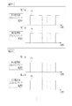
ここで、「各電源部30A、30Bの動作を同期させる」とは、図4、図5に示すように、各撮影で各電源部30A、30Bの動作を同一にするという意味である。さらに言えば、各スイッチング電源47A、47BのパルスPA、PBの出力タイミングを、各撮影で同一にするという意味である。
Here, "synchronizing the operations of the
図4は、各パルスPA、PBの位相が揃っている場合を示す。対して図5は、各パルスPA、PBの位相がずれている場合を示す。このように、たとえ各パルスPA、PBの位相がずれていたとしても、そのずれ方が各撮影で同一であれば、各撮影で各電源部30A、30Bの動作が同一であると言える。
FIG. 4 shows a case where the phases of the pulses PA and PB are aligned. On the other hand, FIG. 5 shows a case where the phases of the pulses PA and PB are out of phase. In this way, even if the phases of the pulses PA and PB are out of phase, if the out-of-phase is the same in each shooting, it can be said that the operations of the
図3に戻って、同期信号供給部50は、各電源部30A、30Bの各スイッチング電源47A、47Bに加えて、各回路部29A、29Bの各ゲート駆動回路45A、45Bと各信号処理回路46A、46Bにも同期信号SYNCを供給する。各ゲート駆動回路45A、45Bは、同期信号SYNCに応じたタイミングでゲートパルスを発する。各信号処理回路46A、46Bは、同期信号SYNCに応じたタイミングで、アナログの電圧信号の出力、相関二重サンプリング、アナログ/デジタル変換等を実行する。すなわち、同期信号SYNCは、各回路部29A、29Bの動作を規定するクロック信号としても利用される。
Returning to FIG. 3, the synchronous
図6において、コンソール16は、第1センサパネル11Aから第1X線画像および第1オフセット画像を、第2センサパネル11Bから第2X線画像および第2オフセット画像をそれぞれ受信する。第1X線画像と第2X線画像は、X線源15から照射されて被写体Hを透過したX線に感応して各画素40A、40Bに蓄積された電荷に基づくもので、被写体Hの体内構造を表すものである。一方、第1オフセット画像と第2オフセット画像は、X線が照射されていない状態で第1センサパネル11Aと第2センサパネル11Bに画像読み出し動作を実行させて得られたもので、固定パターンノイズが乗ったものである。各オフセット画像は、例えば、医療施設の始業時に電子カセッテ10の電源がオンされた場合等に取得される。もちろん、各撮影の都度、各オフセット画像を取得してもよい。
In FIG. 6, the
前述のように、各回路部29A、29B、各電源部30A、30B、および制御部31は、グラウンドリターン経路を共有している。このため、グラウンドリターン経路を介して、各回路部29A、29Bのうちの一方から他方にリターン電流が回り込むことでグラウンド電位が変動する。このグラウンド電位の変動によるノイズは、各回路部29A、29Bと各電源部30A、30Bの相互作用によるノイズであり、各オフセット画像に乗る固定パターンノイズに含まれる。固定パターンノイズには、この他にも、環境温度等の電子カセッテ10の使用環境に起因するノイズもある。
As described above, the
第1オフセット補正部60Aは、第1X線画像から第1オフセット画像を画素単位で減算する。これにより第1X線画像から固定パターンノイズに起因するアーチファクトを除去し、補正済み第1X線画像とする。第2オフセット補正部60Bも同様に、第2X線画像から第2オフセット画像を画素単位で減算することで、第2X線画像から固定パターンノイズに起因するアーチファクトを除去し、補正済み第2X線画像とする。
The first offset
ES画像生成部61は、第1オフセット補正部60Aからの補正済み第1X線画像と、第2オフセット補正部60Bからの補正済み第2X線画像とから、ES画像を生成する。具体的には、ES画像生成部61は、補正済み第2X線画像に所定の係数を乗算したものから、補正済み第1X線画像に所定の係数を乗算したものを画素単位で減算する。こうしたサブトラクション処理で生成されたES画像は、例えば、軟部組織が除去され、骨部組織が強調されたものとなる。
The ES
骨密度算出部62は、骨に関する指標値として、被写体Hの撮影部位における骨密度を算出する。具体的には、骨密度算出部62は、まず、ES画像生成部61からのES画像を解析し、ES画像内の骨部組織の領域を抽出する。そして、例えば骨部組織の領域の画素値の代表値(平均値、最大値、最頻値等)に、画素値を骨量に変換する変換係数を乗算し、骨量を算出する。骨密度算出部62は、算出した骨量を骨部組織の領域の面積で除算することで、骨密度を算出する。
The bone
コンソール16は、骨密度算出部62で算出した骨密度を、ES画像生成部61で生成したES画像等とともにディスプレイ17に表示する。このように、各センサパネル11A、11Bから出力された各X線画像は、骨に関する指標値の算出に利用される。なお、骨密度に加えて、あるいは代えて、骨量をディスプレイ17に表示してもよい。
The
各オフセット補正部60A、60B、ES画像生成部61、骨密度算出部62は、例えば、X線撮影に関わるアプリケーションプログラムを実行することにより、コンソール16のCPU(Central Processing Unit)に構築される。これら各部のうちの一部または全部を電子カセッテ10のCPUに構築し、電子カセッテ10でオフセット補正や骨密度の算出を行っても構わない。
The offset
次に、上記構成による作用を説明する。電子カセッテ10を用いた被写体HのX線撮影を行う場合、オペレータは、電子カセッテ10の電源をオンし、電子カセッテ10を撮影台13のホルダ14にセットする。そして、電子カセッテ10、X線源15、および被写体Hの相互の位置関係を調整した後、X線源15からX線を照射させる。
Next, the operation of the above configuration will be described. When performing X-ray photography of the subject H using the
X線源15から照射されて被写体Hを透過したX線は、透過板25を介して第1センサパネル11Aおよび第2センサパネル11Bに入射される。各センサパネル11A、11Bでは、X線の照射を受けて、画素リセット動作後に画素電荷蓄積動作が実行され、各画素40A、40BにX線の到達線量に応じた電荷が蓄積される。
The X-rays emitted from the X-ray source 15 and transmitted through the subject H are incident on the
X線の照射終了後、各センサパネル11A、11Bでは画像読み出し動作が実行される。これにより、第1センサパネル11Aから第1X線画像が、第2センサパネル11Bから第2X線画像が、それぞれ出力される。
After the X-ray irradiation is completed, the image reading operation is executed on the
図3に示したように、電子カセッテ10では、同期信号供給部50から各電源部30A、30Bの各スイッチング電源47A、47Bに同期信号SYNCが供給される。この同期信号SYNCにより、図4、図5に示したように、各電源部30A、30Bの動作が同期され、各撮影で各電源部30A、30Bの動作が同一とされる。
As shown in FIG. 3, in the
各撮影で各電源部30A、30Bの動作が同一であるため、グラウンド電位の変動によるノイズが各撮影で常に同じとなり、少なくともグラウンド電位の変動によるノイズに起因してX線画像に発生するアーチファクトの変動量を所望の範囲に抑制することが可能となる。したがって、X線画像の再現性を確保することが可能となる。なお、アーチファクトの変動量の所望の範囲は、例えば、JIS(Japanese Industrial Standards)規格Z4930(X線骨密度測定装置用性能評価)の再現性試験の変動係数から導き出した、絶対値で1σ=2LSB(Least Significant Bit)である。
Since the operations of the
また、これも図3に示したように、同期信号供給部50は制御部31に設けられ、かつ、同期信号SYNCは、各回路部29A、29Bの各ゲート駆動回路45A、45Bと各信号処理回路46A、46Bにも供給される。このため、同期信号SYNCを、各電源部30A、30Bの動作を同期させるためだけでなく、各回路部29A、29Bの動作を規定するためにも有効利用することができる。
Further, as also shown in FIG. 3, the synchronization
各X線画像は、電子カセッテ10からコンソール16に送信される。コンソール16では、図6に示したように、各オフセット補正部60A、60Bで各X線画像から固定パターンノイズに起因するアーチファクトが除去される。この際、各回路部29A、29Bと各電源部30A、30Bの相互作用によるノイズであるグラウンド電位の変動によるノイズに起因するアーチファクトも抑制される。
Each X-ray image is transmitted from the
もし各電源部30A、30Bの動作が非同期で、グラウンド電位の変動によるノイズが撮影毎に異なると、各オフセット補正部60A、60Bで除去するアーチファクトの量(各オフセット画像に乗ったグラウンド電位の変動によるノイズの量)も各X線画像の撮影時とは異なることになり、結局はX線画像の再現性を確保することができなくなる。例えば第1オフセット画像に乗ったグラウンド電位の変動によるノイズの量が10で、第1X線画像に乗ったグラウンド電位の変動によるノイズの量が8だった場合は、オフセット補正が行き過ぎたものとなる。対して本発明では、各電源部30A、30Bの動作を同期させているので、そうした事態は起こらない。なお、X線画像の再現性を確保するとは、グラウンド電位の変動によるノイズに起因してX線画像に重畳するアーチファクトの変動量を所望の範囲に抑制することと同義である。
If the operations of the
オフセット補正後、コンソール16では、ES画像生成部61でES画像が生成され、さらにES画像に基づいて骨密度算出部62で骨密度が算出される。骨密度はES画像等とともにディスプレイ17に表示される。
After the offset correction, in the
骨密度といった骨に関する指標値の算出の元となるX線画像の再現性が確保できていないと、指標値の信頼性が大きく低下するおそれがある。しかしながら、本発明では、X線画像の再現性が確保されているので、指標値の信頼性を向上させることができる。 If the reproducibility of the X-ray image, which is the basis for calculating the index value related to bone such as bone density, cannot be ensured, the reliability of the index value may be significantly reduced. However, in the present invention, since the reproducibility of the X-ray image is ensured, the reliability of the index value can be improved.
また、各センサパネル11A、11Bを厚さ方向に順に配置した構成では、第2センサパネル11Bへの到達線量は、第1センサパネル11Aへの到達線量の10〜20%と、どうしても低下してしまう。このため、第2X線画像のSN(Signal-Noise)比は低くなり、グラウンド電位の変動によるノイズの影響が比較的高くなる。したがって、各センサパネル11A、11Bを厚さ方向に順に配置した構成に本発明を適用すれば、より大きな効果を発揮することができる。
Further, in the configuration in which the
[第2実施形態]
図7に示す第2実施形態では、制御部31ではなく、第1電源部30Aに同期信号供給部50を設ける。この場合、同期信号供給部50は、同じ第1電源部30A内にある第1スイッチング電源47A、第2電源部30Bの第2スイッチング電源47B、および制御部31に同期信号SYNCを供給する。制御部31は、同期信号供給部50からの同期信号SYNCを、上記第1実施形態と同じく、クロック信号として各回路部29A、29Bに供給する。
[Second Embodiment]
In the second embodiment shown in FIG. 7, the synchronization
第1スイッチング電源47Aは、自らが属する第1電源部30A内にある同期信号供給部50から同期信号SYNCが供給されるので、いわば自励式である。一方、第2スイッチング電源47Bは、自らが属する第2電源部30Bとは別の第1電源部30A内にある同期信号供給部50から同期信号SYNCが供給されるので、いわば他励式である。この考え方を上記第1実施形態に当て嵌めると、上記第1実施形態では、各スイッチング電源47A、47Bは、制御部31内にある同期信号供給部50から同期信号SYNCが供給されるので、いずれも他励式である。
The first
なお、同期信号供給部50は、第1電源部30Aではなく、第2電源部30Bに設けられていてもよい。すなわち、同期信号供給部50は、各電源部30A、30Bのうちの一つに設けられていてもよい。また、同期信号供給部50は、各電源部30A、30B、制御部31とは別に独立して設けられていてもよい。
The synchronization
[第3実施形態]
図8および図9に示す第3実施形態は、図1等に示したように複数のセンサパネルを厚さ方向TDに順に配置する形態ではなく、複数のセンサパネルを、厚さ方向TD(図8では紙面に直交する方向)と直交する同一平面上に敷き詰める形態である。
[Third Embodiment]
The third embodiment shown in FIGS. 8 and 9 is not a form in which a plurality of sensor panels are sequentially arranged in the thickness direction TD as shown in FIG. 1 and the like, but a plurality of sensor panels are arranged in the thickness direction TD (FIG. 8). In No. 8, it is a form of laying on the same plane orthogonal to the direction orthogonal to the paper surface).
図8は、本実施形態の電子カセッテ70を、X線が入射する前面側からみた図である。電子カセッテ70には、上記第1実施形態の電子カセッテ10と同様、前面の開口にX線透過性を有する透過板71が取り付けられている。そして、第1センサパネル72A、第2センサパネル72B、第3センサパネル72C、第4センサパネル72Dの計四つのセンサパネル72を、厚さ方向TDと直交する同一平面上に敷き詰めた構成である。
FIG. 8 is a view of the
この場合、図9に示すように、第1センサパネル72A〜第4センサパネル72D毎に、第1回路部75A、第2回路部75B、第3回路部75C、第4回路部75Dが設けられる。また、第1センサパネル72A〜第4センサパネル72Dと第1回路部75A〜第4回路部75Dのペア毎に、第1電源部76A、第2電源部76B、第3電源部76C、第4電源部76Dが設けられる。そして、制御部77に設けられた同期信号供給部80から、各回路部75A〜75Dおよび各電源部76A〜76Dに同期信号SYNCが供給される。なお、上記第2実施形態を適用して、同期信号供給部80を各電源部76A〜76Dのうちの一つに設けてもよい。
In this case, as shown in FIG. 9, the
各センサパネル72A〜72Dは、一回のX線の照射で画素に同時に電荷を蓄積する。こうして各センサパネル72A〜72Dから検出された第1X線画像、第2X線画像、第3X線画像、第4X線画像は、制御部77を介してコンソール16に送信される。コンソール16は、各X線画像を各センサパネル72A〜72Dの並びに対応する位置で繋ぎ合わせ、一枚のX線画像を生成し、これをディスプレイ17に表示する。このように、複数のセンサパネルは、上記第1実施形態のように厚さ方向に順に配置されていてもよいし、本実施形態のように同一平面上に敷き詰められていてもよい。
Each of the
なお、「複数のセンサパネルが厚さ方向に順に配置」されている状態とは、上記各実施形態の複数のセンサパネルが密着して配置されている状態に限らない。複数のセンサパネルが密着しておらず、複数のセンサパネルが隙間で隔てられている状態や、複数のセンサパネルの間に、X線の軟線成分の入射を制限するX線フィルタ等の介挿物がある状態も含む。 The state in which "a plurality of sensor panels are arranged in order in the thickness direction" is not limited to a state in which the plurality of sensor panels of each of the above embodiments are arranged in close contact with each other. A state in which a plurality of sensor panels are not in close contact with each other and the plurality of sensor panels are separated by a gap, or an X-ray filter or the like that limits the incidence of soft X-ray components is inserted between the plurality of sensor panels. Including the state where there is an object.
上記各実施形態では、放射線画像検出装置として電子カセッテを例示したが、本発明はこれに限定されない。撮影台に固定される据え置き型の放射線画像検出装置に対しても、本発明は適用することが可能である。また、本発明は、X線に限らず、γ線等の他の放射線を使用する場合にも適用することができる。 In each of the above embodiments, an electronic cassette has been exemplified as a radiographic image detection device, but the present invention is not limited thereto. The present invention can also be applied to a stationary radiographic image detection device fixed to a photographing table. Further, the present invention can be applied not only to X-rays but also to the case of using other radiation such as γ-rays.
なお、本明細書中に記載の「あるいは」、「または」なる接続詞は、文脈によっては、これらの接続詞で繋げられた複数の選択肢のうちのいずれか一つ、という限定的解釈を意図する表現ではなく、複数の選択肢の組み合わせも含む表現である。例えば、「選択肢A、あるいは選択肢Bを行う。」という文章は、文脈によっては、「選択肢Aを行う。」、「選択肢Bを行う。」、「選択肢Aおよび選択肢Bを行う。」の三通りの意があると解釈すべきである。 It should be noted that the conjunction "or" or "or" described in the present specification is an expression intended for a limited interpretation of any one of a plurality of options connected by these conjunctions, depending on the context. It is not an expression that includes a combination of multiple options. For example, the sentence "perform option A or option B." may have three ways, "perform option A", "perform option B", and "perform option A and option B", depending on the context. Should be interpreted as having the meaning of.
本発明は、上記各実施形態に限らず、本発明の要旨を逸脱しない限り種々の構成を採用し得ることはもちろんである。 It goes without saying that the present invention is not limited to each of the above embodiments, and various configurations can be adopted as long as the gist of the present invention is not deviated.
10、70 電子カセッテ(放射線画像検出装置)
11A 第1センサパネル
11B 第2センサパネル
12 筐体
13 撮影台
14 ホルダ
15 X線源(放射線源)
16 コンソール
17 ディスプレイ
18 入力デバイス
25、71 透過板
26A、26B 第1、第2光検出基板
27A、27B 第1、第2シンチレータ
28 基台
29A、29B 第1、第2回路部
30A、30B 第1、第2電源部
31、77 制御部
40A、40B 第1、第2画素
41A、41B 第1、第2ゲート線
42A、42B 第1、第2信号線
43A、43B 第1、第2光電変換部
44A、44B 第1、第2TFT
45A、45B 第1、第2ゲート駆動回路
46A、46B 第1、第2信号処理部
47A、47B 第1、第2スイッチング電源
50、80 同期信号供給部
60A、60B 第1、第2オフセット補正部
61 ES画像生成部
62 骨密度算出部
72A〜72D 第1〜第4センサパネル
75A〜75D 第1〜第4回路部
76A〜76D 第1〜第4電源部
H 被写体
TD 厚さ方向
X 画素の行方向
Y 画素の列方向
SYNC 同期信号
PA、PB 第1、第2スイッチング電源のパルス
10,70 Electronic cassette (radiation image detector)
11A
16
45A, 45B 1st and 2nd
Claims (6)
複数の前記センサパネル毎に設けられ、前記電荷をデジタル信号に変換して放射線画像として出力する複数の回路部と、
前記センサパネルと前記回路部のペア毎に設けられ、前記センサパネルと前記回路部の前記ペアにそれぞれ給電する複数の電源部と、
複数の前記電源部の動作を同期させる同期信号を、複数の前記電源部に供給する同期信号供給部とを備える放射線画像検出装置。 A plurality of sensor panels in which pixels that accumulate charges in response to radiation emitted from a radiation source and transmitted through the subject are arranged in two dimensions, and
A plurality of circuit units provided for each of the plurality of sensor panels, which convert the electric charge into a digital signal and output it as a radiographic image.
A plurality of power supply units provided for each pair of the sensor panel and the circuit unit to supply power to the pair of the sensor panel and the circuit unit, respectively.
A radiation image detection device including a synchronization signal supply unit that supplies synchronization signals for synchronizing the operations of the plurality of power supply units to the plurality of power supply units.
前記同期信号供給部は、前記制御部に設けられている請求項1に記載の放射線画像検出装置。 A control unit for controlling the operation of the sensor panel is provided.
The radiographic image detection device according to claim 1, wherein the synchronization signal supply unit is provided in the control unit.
Priority Applications (3)
| Application Number | Priority Date | Filing Date | Title |
|---|---|---|---|
| JP2018039373A JP6869914B2 (en) | 2018-03-06 | 2018-03-06 | Radiation image detector |
| US16/292,653 US10838079B2 (en) | 2018-03-06 | 2019-03-05 | Radiographic image detection device |
| CN201910162820.3A CN110243845B (en) | 2018-03-06 | 2019-03-05 | Radiographic image detection device |
Applications Claiming Priority (1)
| Application Number | Priority Date | Filing Date | Title |
|---|---|---|---|
| JP2018039373A JP6869914B2 (en) | 2018-03-06 | 2018-03-06 | Radiation image detector |
Publications (3)
| Publication Number | Publication Date |
|---|---|
| JP2019152594A JP2019152594A (en) | 2019-09-12 |
| JP2019152594A5 JP2019152594A5 (en) | 2020-03-19 |
| JP6869914B2 true JP6869914B2 (en) | 2021-05-12 |
Family
ID=67843262
Family Applications (1)
| Application Number | Title | Priority Date | Filing Date |
|---|---|---|---|
| JP2018039373A Active JP6869914B2 (en) | 2018-03-06 | 2018-03-06 | Radiation image detector |
Country Status (3)
| Country | Link |
|---|---|
| US (1) | US10838079B2 (en) |
| JP (1) | JP6869914B2 (en) |
| CN (1) | CN110243845B (en) |
Families Citing this family (1)
| Publication number | Priority date | Publication date | Assignee | Title |
|---|---|---|---|---|
| EP3835829A1 (en) * | 2019-12-09 | 2021-06-16 | Koninklijke Philips N.V. | X-ray detector |
Family Cites Families (12)
| Publication number | Priority date | Publication date | Assignee | Title |
|---|---|---|---|---|
| JP3847889B2 (en) * | 1997-04-08 | 2006-11-22 | キヤノン株式会社 | Photoelectric conversion device |
| JP3890210B2 (en) * | 2000-08-11 | 2007-03-07 | キヤノン株式会社 | Image capturing apparatus and method for controlling image capturing apparatus |
| CN100482168C (en) * | 2004-11-30 | 2009-04-29 | 株式会社东芝 | X-ray calculation tomographic scanner and x-ray detecting system |
| JP2010014415A (en) * | 2008-07-01 | 2010-01-21 | Toshiba Corp | Radiation detector, and radiation diagnostic equipment |
| JP5438714B2 (en) * | 2011-03-31 | 2014-03-12 | 富士フイルム株式会社 | Radiography equipment |
| CN103995278A (en) * | 2014-05-07 | 2014-08-20 | 东北大学 | Double-energy linear array detector for X-ray safety check device |
| CN106456081B (en) * | 2014-05-27 | 2019-11-01 | 爱克发有限公司 | It is multiple wireless from the method for triggering radiographic images sensor for being controlled in single exposure |
| JP2017192090A (en) * | 2016-04-15 | 2017-10-19 | 東芝電子管デバイス株式会社 | Radiation detector |
| JP6695232B2 (en) * | 2016-07-29 | 2020-05-20 | 富士フイルム株式会社 | Radiography system |
| JP6639353B2 (en) | 2016-07-29 | 2020-02-05 | 富士フイルム株式会社 | Radiation image capturing system, radiation image capturing method, and radiation image capturing program |
| JP6549535B2 (en) * | 2016-07-29 | 2019-07-24 | 富士フイルム株式会社 | Radiation imaging system, image processing method, and image processing program |
| JP6493893B2 (en) * | 2017-09-06 | 2019-04-03 | 富士フイルム株式会社 | Radiographic imaging apparatus and radiographic imaging system |
-
2018
- 2018-03-06 JP JP2018039373A patent/JP6869914B2/en active Active
-
2019
- 2019-03-05 US US16/292,653 patent/US10838079B2/en active Active
- 2019-03-05 CN CN201910162820.3A patent/CN110243845B/en active Active
Also Published As
| Publication number | Publication date |
|---|---|
| CN110243845B (en) | 2024-03-12 |
| CN110243845A (en) | 2019-09-17 |
| US20190277979A1 (en) | 2019-09-12 |
| US10838079B2 (en) | 2020-11-17 |
| JP2019152594A (en) | 2019-09-12 |
Similar Documents
| Publication | Publication Date | Title |
|---|---|---|
| JP5666716B2 (en) | Radiation moving image processing apparatus, radiation moving image capturing apparatus, radiation moving image capturing system, radiation moving image processing method, radiation moving image processing program, and storage medium | |
| JP5562767B2 (en) | Radiographic imaging system and radiographic imaging method | |
| US6952464B2 (en) | Radiation imaging apparatus, radiation imaging system, and radiation imaging method | |
| JP5859934B2 (en) | Radiation imaging system and operation method thereof, radiation image detection apparatus and operation program thereof | |
| JP5878444B2 (en) | Radiation image detection device | |
| JP5376897B2 (en) | Radiation imaging equipment | |
| JP5797630B2 (en) | Radiation image capturing apparatus, pixel value acquisition method, and program | |
| JP2012125409A (en) | X-ray imaging apparatus | |
| JP2012045044A (en) | Radiation image detection device | |
| US10754047B2 (en) | Radiographic image detection device | |
| JP2011212427A (en) | Radiation imaging system | |
| JP6869914B2 (en) | Radiation image detector | |
| JP2012247401A (en) | Radiographic apparatus | |
| JP6932095B2 (en) | Radiation image detector | |
| JP6987674B2 (en) | Radiation image detection device | |
| JP5634894B2 (en) | Radiation imaging apparatus and program | |
| JP5489951B2 (en) | Imaging area specifying device, radiographic imaging system, and imaging area specifying method | |
| WO2013136597A1 (en) | Radiography control device, radiography system, radiography device control method, and radiography control program | |
| JP5615664B2 (en) | Radiography equipment | |
| JP2013180050A (en) | Radiographic imaging control device, radiation image photographing system, control method for radiographic apparatus and control program for radiation image photographing | |
| JP5626225B2 (en) | Radiographic imaging apparatus and radiographic imaging system | |
| WO2013062052A1 (en) | Radiographic display system, radiographic display device, radiographic imaging device, program, radiograph display method, and recording medium | |
| WO2013125111A1 (en) | Radiographic imaging control device, radiographic imaging system, control method for radiographic imaging device, and control program for radiographic imaging | |
| WO2012056950A1 (en) | Radiation detector and radiographic imaging device | |
| JP2014178116A (en) | Radiographic imaging apparatus and radiographic image detection apparatus |
Legal Events
| Date | Code | Title | Description |
|---|---|---|---|
| A521 | Request for written amendment filed |
Free format text: JAPANESE INTERMEDIATE CODE: A523 Effective date: 20200205 |
|
| A621 | Written request for application examination |
Free format text: JAPANESE INTERMEDIATE CODE: A621 Effective date: 20200205 |
|
| A977 | Report on retrieval |
Free format text: JAPANESE INTERMEDIATE CODE: A971007 Effective date: 20210114 |
|
| TRDD | Decision of grant or rejection written | ||
| A01 | Written decision to grant a patent or to grant a registration (utility model) |
Free format text: JAPANESE INTERMEDIATE CODE: A01 Effective date: 20210323 |
|
| A61 | First payment of annual fees (during grant procedure) |
Free format text: JAPANESE INTERMEDIATE CODE: A61 Effective date: 20210414 |
|
| R150 | Certificate of patent or registration of utility model |
Ref document number: 6869914 Country of ref document: JP Free format text: JAPANESE INTERMEDIATE CODE: R150 |
|
| R250 | Receipt of annual fees |
Free format text: JAPANESE INTERMEDIATE CODE: R250 |