EP3835829A1 - X-ray detector - Google Patents
X-ray detector Download PDFInfo
- Publication number
- EP3835829A1 EP3835829A1 EP19214388.1A EP19214388A EP3835829A1 EP 3835829 A1 EP3835829 A1 EP 3835829A1 EP 19214388 A EP19214388 A EP 19214388A EP 3835829 A1 EP3835829 A1 EP 3835829A1
- Authority
- EP
- European Patent Office
- Prior art keywords
- layer
- scintillator
- ray detector
- photodiode array
- photodiode
- Prior art date
- Legal status (The legal status is an assumption and is not a legal conclusion. Google has not performed a legal analysis and makes no representation as to the accuracy of the status listed.)
- Withdrawn
Links
Images


Classifications
-
- G—PHYSICS
- G01—MEASURING; TESTING
- G01T—MEASUREMENT OF NUCLEAR OR X-RADIATION
- G01T1/00—Measuring X-radiation, gamma radiation, corpuscular radiation, or cosmic radiation
- G01T1/16—Measuring radiation intensity
- G01T1/20—Measuring radiation intensity with scintillation detectors
- G01T1/2018—Scintillation-photodiode combinations
- G01T1/20181—Stacked detectors, e.g. for measuring energy and positional information
-
- A—HUMAN NECESSITIES
- A61—MEDICAL OR VETERINARY SCIENCE; HYGIENE
- A61B—DIAGNOSIS; SURGERY; IDENTIFICATION
- A61B6/00—Apparatus for radiation diagnosis, e.g. combined with radiation therapy equipment
- A61B6/02—Devices for diagnosis sequentially in different planes; Stereoscopic radiation diagnosis
- A61B6/03—Computerised tomographs
- A61B6/032—Transmission computed tomography [CT]
-
- A—HUMAN NECESSITIES
- A61—MEDICAL OR VETERINARY SCIENCE; HYGIENE
- A61B—DIAGNOSIS; SURGERY; IDENTIFICATION
- A61B6/00—Apparatus for radiation diagnosis, e.g. combined with radiation therapy equipment
- A61B6/42—Apparatus for radiation diagnosis, e.g. combined with radiation therapy equipment with arrangements for detecting radiation specially adapted for radiation diagnosis
- A61B6/4208—Apparatus for radiation diagnosis, e.g. combined with radiation therapy equipment with arrangements for detecting radiation specially adapted for radiation diagnosis characterised by using a particular type of detector
- A61B6/4241—Apparatus for radiation diagnosis, e.g. combined with radiation therapy equipment with arrangements for detecting radiation specially adapted for radiation diagnosis characterised by using a particular type of detector using energy resolving detectors, e.g. photon counting
-
- A—HUMAN NECESSITIES
- A61—MEDICAL OR VETERINARY SCIENCE; HYGIENE
- A61B—DIAGNOSIS; SURGERY; IDENTIFICATION
- A61B6/00—Apparatus for radiation diagnosis, e.g. combined with radiation therapy equipment
- A61B6/48—Diagnostic techniques
- A61B6/482—Diagnostic techniques involving multiple energy imaging
-
- G—PHYSICS
- G01—MEASURING; TESTING
- G01T—MEASUREMENT OF NUCLEAR OR X-RADIATION
- G01T1/00—Measuring X-radiation, gamma radiation, corpuscular radiation, or cosmic radiation
- G01T1/16—Measuring radiation intensity
- G01T1/20—Measuring radiation intensity with scintillation detectors
- G01T1/2002—Optical details, e.g. reflecting or diffusing layers
-
- G—PHYSICS
- G01—MEASURING; TESTING
- G01T—MEASUREMENT OF NUCLEAR OR X-RADIATION
- G01T1/00—Measuring X-radiation, gamma radiation, corpuscular radiation, or cosmic radiation
- G01T1/16—Measuring radiation intensity
- G01T1/20—Measuring radiation intensity with scintillation detectors
- G01T1/2006—Measuring radiation intensity with scintillation detectors using a combination of a scintillator and photodetector which measures the means radiation intensity
-
- G—PHYSICS
- G01—MEASURING; TESTING
- G01T—MEASUREMENT OF NUCLEAR OR X-RADIATION
- G01T1/00—Measuring X-radiation, gamma radiation, corpuscular radiation, or cosmic radiation
- G01T1/16—Measuring radiation intensity
- G01T1/20—Measuring radiation intensity with scintillation detectors
- G01T1/2008—Measuring radiation intensity with scintillation detectors using a combination of different types of scintillation detectors, e.g. phoswich
-
- G—PHYSICS
- G01—MEASURING; TESTING
- G01T—MEASUREMENT OF NUCLEAR OR X-RADIATION
- G01T1/00—Measuring X-radiation, gamma radiation, corpuscular radiation, or cosmic radiation
- G01T1/16—Measuring radiation intensity
- G01T1/20—Measuring radiation intensity with scintillation detectors
- G01T1/2018—Scintillation-photodiode combinations
- G01T1/20183—Arrangements for preventing or correcting crosstalk, e.g. optical or electrical arrangements for correcting crosstalk
-
- G—PHYSICS
- G01—MEASURING; TESTING
- G01T—MEASUREMENT OF NUCLEAR OR X-RADIATION
- G01T1/00—Measuring X-radiation, gamma radiation, corpuscular radiation, or cosmic radiation
- G01T1/16—Measuring radiation intensity
- G01T1/20—Measuring radiation intensity with scintillation detectors
- G01T1/2018—Scintillation-photodiode combinations
- G01T1/20184—Detector read-out circuitry, e.g. for clearing of traps, compensating for traps or compensating for direct hits
-
- G—PHYSICS
- G01—MEASURING; TESTING
- G01T—MEASUREMENT OF NUCLEAR OR X-RADIATION
- G01T1/00—Measuring X-radiation, gamma radiation, corpuscular radiation, or cosmic radiation
- G01T1/16—Measuring radiation intensity
- G01T1/20—Measuring radiation intensity with scintillation detectors
- G01T1/2018—Scintillation-photodiode combinations
- G01T1/20186—Position of the photodiode with respect to the incoming radiation, e.g. in the front of, below or sideways the scintillator
-
- G—PHYSICS
- G01—MEASURING; TESTING
- G01T—MEASUREMENT OF NUCLEAR OR X-RADIATION
- G01T1/00—Measuring X-radiation, gamma radiation, corpuscular radiation, or cosmic radiation
- G01T1/16—Measuring radiation intensity
- G01T1/20—Measuring radiation intensity with scintillation detectors
- G01T1/2018—Scintillation-photodiode combinations
- G01T1/20187—Position of the scintillator with respect to the photodiode, e.g. photodiode surrounding the crystal, the crystal surrounding the photodiode, shape or size of the scintillator
-
- G—PHYSICS
- G01—MEASURING; TESTING
- G01T—MEASUREMENT OF NUCLEAR OR X-RADIATION
- G01T1/00—Measuring X-radiation, gamma radiation, corpuscular radiation, or cosmic radiation
- G01T1/16—Measuring radiation intensity
- G01T1/20—Measuring radiation intensity with scintillation detectors
- G01T1/2018—Scintillation-photodiode combinations
- G01T1/20188—Auxiliary details, e.g. casings or cooling
Definitions
- the present invention relates to an X-ray detector, and to an X-ray detector system.
- X-ray detectors for spectral energy computer tomography and/or X-ray applications, comprising two or more scintillator layers and associated photo diode arrays, are very expensive.
- Low-cost photodiodes for example based on an organic layer - OPD - or amorphous silicon (a-Si), have a relatively high defect density in the bulk, where charge can be trapped at defect sites and released at a later time. Because of such an issue leading to image artefacts, these detectors cannot find utility in these specialized applications.
- an X-ray detector comprising:
- the first scintillator is configured to absorb X-rays from an X-ray pulse and (in response thereto) to emit light.
- the first photodiode array is positioned adjacent to the first scintillator.
- the first photodiode array is configured to detect at least some of the light emitted by the first scintillator.
- the second scintillator is configured to absorb X-rays from the X-ray pulse and (in response thereto) to emit light.
- the second photodiode array is positioned adjacent to the second scintillator.
- the second photodiode array is configured to detect at least some of the light emitted by the second scintillator.
- the at least one layer is configured to emit radiation.
- the at least one layer is configured such that at least some of the emitted radiation irradiates the first photodiode array and at least some of the emitted radiation irradiates the second photodiode array.
- a dual layer detector for example for computed tomography dual energy applications, can utilize low-cost photodiodes (based on for example an organic layer OPD or a-Si).
- low-cost photodiodes based on for example an organic layer OPD or a-Si.
- a light emitting layer is provided that can for example emit visible and ultraviolet light below 750nm to fill defect sites, or infrared radiation for example above 750nm to fill traps within the bandgap. This means that problems such as a change in effective gain (or detective efficiency) and/or a change in the step response for such low-cost detectors is mitigated.
- the first photodiode array being positioned adjacent to the first scintillator does not preclude another element of the X-ray detector being between the first photodiode array and the first scintillator.
- the second photodiode array being positioned adjacent to the second scintillator does not preclude another element of the X-ray detector being between the second photodiode array and the second scintillator.
- the at least one layer is configured to emit radiation at infrared wavelengths, and/or the at least one layer is configured to emit radiation at visible and/or the at least one layer is configured to emit radiation at ultraviolet wavelengths.
- the at least one layer is positioned between the first photodiode and the second photodiode.
- the at least one layer being positioned between the first photodiode and the second photodiode does not preclude another element of the X-ray detector being between the at least one layer and the first photodiode.
- the at least one layer being positioned between the first photodiode and the second photodiode does not preclude another element of the X-ray detector being between the at least one layer and the second photodiode.
- the at least one layer is configured such that a transmission of the at least one layer in a direction from the first photodiode array to the second photodiode array for light emitted by the first scintillator and/or for light emitted by the second scintillator is less than 10%, preferable less than 5%, more preferably less than 1%.
- a first layer of the at least one layer is positioned below the first photodiode and a second layer of the at least one layer is positioned below the second photodiode.
- a bottom surface of that layer can be made as a reflector for example or radiation blocker.
- This reflector or radiation blocker stops radiation from one scintillator being detected by the photodiode array associated with the other scintillator. If reflectors are used then these can be used for both layers and maximize the amount of radiation emitted in the direction of the associated photodiode array for that layer.
- the first layer of the at least one layer being positioned below the first photodiode does not preclude another element of the X-ray detector being between the first layer and the first photodiode.
- the second layer of the at least one layer being positioned below the second photodiode does not preclude another element of the X-ray detector being between the second layer and the second photodiode.
- the at least one layer comprises at least one glass or polymer plate.
- At least one light source is configured to generate the radiation that is emitted by the at least one layer.
- the at least one light source can be at least one LED.
- the at least one light source is positioned proximate to at least one edge of the at least one layer.
- the at least one edge of the at least one layer is mirrored.
- mirrored means that the at least one edge can be supplied with a reflective coating, or given a mirror finish.
- At least one face of the at least one layer substantially perpendicular to the at least one edge is roughened.
- the at least one LED is integrated into the at least one layer.
- the at least one layer comprises at least one OLED layer.
- a first surface of the first photodiode array faces the first scintillator and a second surface of the first photodiode array faces away from the first scintillator and a first surface of the second photodiode array faces the second surface of the first photodiode array.
- a first electrode is in contact with the second surface of the first photodiode array and a second electrode is in contact with the first surface of the second photodiode array.
- electrodes that are used as part of the biasing potential for the photodiode arrays can also be used as part of the power supply for light emitting means such as LEDs associated with the at least one layer.
- the first electrode and second electrode are in contact with the at least one layer.
- an X-ray detector system comprising an X-ray detector according to the first aspect; and a processing unit configured to control the X-ray detector such that the at least one layer does not emit radiation when the X-ray source is emitting X-rays.
- an X-ray detector system comprising an X-ray source; and an X-ray detector according to the first aspect.
- the X-ray detector system may also include the processing unit configured to control the X-ray detector such that the at least one layer does not emit radiation when the X-ray source is emitting X-rays.
- the light emitting layer can operate continuously, however the photodiode arrays can generate an offset current when the x-ray sources operating that can be considered as a source of noise, however now the layer operates to mitigate the effect of defects only when the x-ray source is not operating.
- the layer(s) does not provide illumination to the photodiode arrays during x-ray radiation, and can otherwise be permanently on.
- Fig. 1 shows an example of an X-ray detector 10.
- the X-ray detector comprises a first scintillator 20, a second scintillator 30, a first photodiode array 40, a second photodiode array 50, and at least one layer 60.
- the first scintillator is configured to absorb X-rays from an X-ray pulse and emit light.
- the first photodiode array is positioned adjacent to the first scintillator.
- the first photodiode array is configured to detect at least some of the light emitted by the first scintillator.
- the second scintillator is configured to absorb X-rays from the X-ray pulse and emit light.
- the second photodiode array is positioned adjacent to the second scintillator.
- the second photodiode array is configured to detect at least some of the light emitted by the second scintillator.
- the at least one layer is configured to emit radiation.
- the at least one layer is configured such that at least some of the emitted radiation from the at least one layer irradiates the first photodiode array and at least some of the emitted radiation from the at least one layer irradiates the second photodiode array.
- the at least one layer has a thickness no greater than 0.5mm.
- the at least one layer has a thickness no greater than 0.3mm.
- the at least one layer comprises at least one light plate.
- the at least one layer is configured to emit radiation at infrared wavelengths, and/or the at least one layer is configured to emit radiation at visible and/or the at least one layer is configured to emit radiation at ultraviolet wavelengths.
- the visible and/or UV radiation is below 750nm.
- the infrared radiation is above 750nm.
- the at least one layer is positioned between the first photodiode and the second photodiode.
- the at least one layer is configured such that a transmission of the at least one layer in a direction from the first photodiode array to the second photodiode array for light emitted by the first scintillator is less than 10%, preferable less than 5%, more preferably less than 1%.
- the at least one layer is configured such that a transmission of the at least one layer in a direction from the second photodiode array to the first photodiode array for light emitted by the second scintillator is less than 10%, preferable less than 5%, more preferably less than 1%.
- a first layer 62 of the at least one layer is positioned below the first photodiode and a second layer 64 of the at least one layer is positioned below the second photodiode.
- Fig. 7 described below shows a possible embodiment of this example.
- the at least one layer comprises at least one glass or polymer plate, and at least one light source 90 is configured to generate the radiation that is emitted by the at least one layer.
- the at least one light source can be at least one light emitting diode (LED).
- the at least one light source is positioned proximate to at least one edge of the at least one layer.
- the at least one light source such as one or more LEDs, can be external to a layer, transmitting light into layer, or can be embedded within the layer near to the edge of the layer.
- the light sources e.g. LEDs
- the light sources are within the layer and at least one edge of the at least one layer is mirrored 100.
- light sources e.g. LEDs
- LEDs can be external to a layer injecting light into the layer to an edge that is not mirrored, whilst other edges of the layer can be mirrored.
- At least one face of the at least one layer substantially perpendicular to the at least one edge is roughened.
- the at least one light source such as at least one LED is integrated into the at least one layer.
- the at least one layer comprises at least one organic light emitting diode (OLED) layer.
- OLED organic light emitting diode
- a first surface of the first photodiode array faces the first scintillator and a second surface of the first photodiode array faces away from the first scintillator and a first surface of the second photodiode array faces the second surface of the first photodiode array, and wherein a first electrode (70) is in contact with the second surface of the first photodiode array and a second electrode (80) is in contact with the first surface of the second photodiode array.
- the first electrode and second electrode are in contact with the at least one layer.
- Fig. 2 shows an example of an X-ray detector system 200.
- the X-ray detector system comprises an X-ray source 210, and an X-ray detector 10 as described above with respect to Fig. 1 .
- the X-ray detector system 200 comprises a processing unit 220.
- the processing unit is configured to control the X-ray detector such that the at least one layer does not emit radiation when the X-ray source is emitting X-rays.
- LEDs producing the light that is emitted by the at least one layer are controlled so as not to emit light when the X-ray source is emitting X-rays.
- the most relevant non-ideal behavior relates to the PDA temporal characteristics.
- the effective gain (or detective efficiency) and the step response may appear to change over time due to charge trapping in the active area. Since these photodiodes can have a relatively high defect density in the bulk, charge can be trapped at the defect sites and only released at a comparatively very long time scale. This can cause ghosting-like artefacts, but also image artefacts, e.g. band artefacts in CT. Methods to counteract the temporal artefacts due to charge trapping are known, e.g. switching off bias; or short forward biasing intervals. Solutions for dual-layer detector applications involving bias light / backlighting have however up until now been lacking.
- the present detector addresses this through a special arrangement of layers with one or more light emitting layers within detector arrangement used for "backlighting" of low-cost photodiodes used to detect radiation emitted from scintillators, where such low-cost photodiodes can be based on OPD or a-Si.
- the inventors realized that by using a light wavelength with energy above the material bandgap (i.e. red light below 800 nm, the defect sites in the photodiodes used within the x-ray detector can be filled prior to X-ray illumination. Having filled the traps, it implies that no further trapping may occur and no changes of the detection efficiency may be perceived during the X-ray illumination. Furthermore, by doing so before every X-ray scan, it ensures that the same initial conditions are met for every image task. Furthermore, the inventors realized that illumination in the infrared sub-band (e.g. IR > 900 nm) can also be used in order to fill traps within the bandgap.
- a light wavelength with energy above the material bandgap i.e. red light below 800 nm
- pulsed operation of light emission within the new detector is not essential, and continuous backlight illumination can be considered.
- the red and/or infrared illumination can remain on all the time.
- the photodiode generates an offset current corresponding to the responsivity to the light, which may be considered as a source of noise.
- the pulsed backlight illumination as discussed above finds utility, where the illumination is switched off during the X-ray irradiation, and otherwise permanently on.
- Fig. 3 shows an example of the new type of X-ray detector 10.
- the X-ray detector has a top layer scintillator 20, with a low-cost photodiode array 40 positioned adjacent to the top layer scintillator to detect radiation emitted from the scintillator resulting from the absorption of x-rays.
- the X-ray detector also has a bottom there scintillator 30, with another low-cost photodiode array 50 positioned adjacent to the bottom there scintillator detect radiation emitted from the scintillator resulting from the absorption of x-rays.
- a glass plate 60 is introduced between both photodiode arrays, which acts as a light emitting layer 60.
- the plate has integrated LEDs 90 and it serves as a diffusion plate such that the two PDA arrays are homogenously illuminated, thereby filling the defect sites and/or filling traps depending upon the wavelength of emission of the LEDs as discussed above.
- Other materials alternative to glass can be used for example, thick polymers, PMMA, etc.
- the glass plate 60 acts as a mechanical support and infrared and/or red light, diffusion based light emitting layer.
- the electrodes 70 and 80 are flex foil electrodes (base substrate material) which are sufficiently transparent to let most of the IR illuminate the photodiode arrays.
- the PDAs can be taken to be "back" illuminated by the light emitting layer 60 (for light proceeding from the scintillator).
- the flex foil may be on top of the PDA (front-illuminated type) and it only requires being optically transparent (e.g. ITO routing).
- the glass plate is in direct contact with the PDA array.
- flex substrates can carry the supply voltage to the LEDs of the glass plate as well as provide bias voltages to the PDAs. Since the glass plate is "sandwiched" between two flex foils, each foil can carry one of the supplies, e.g. common cathode top and common anode bottom, or vice versa.
- the glass can cause some undesirable X-ray absorption. It is therefore of benefit that the glass substrate be kept as thin as possible. Ideally, it should not be thicker than 0.5 mm, preferably thinner than 0.3 mm.
- the embodiments shown in Figs 3 and 4 due to the almost transparent nature of the PDA (particularly OPD), light crosstalk can occur across both scintillator layers, deteriorating the energy separation of the dual layer detector.
- the glass surfaces can be treated to have a transmission, across the interface, of for example only 10%. The remaining light can be reflected and/or absorbed. With a 10 % transmission on each glass surface/interface, the crosstalk across both layers is constrained to well below 1%, since light trying to travel from one scintillator to the other scintillator's photodiode will have to cross two successive interfaces with 10% transmission.
- the LED array providing radiation for the glass light emitting layer in such a situation may need to provide more light to compensate for the lack of transmission at the exit surfaces of the glass layer.
- the flex foil electrodes for as shown in Fig. 4 are now positioned between the photodiode arrays and the scintillators.
- Figs 5 and 6 show examples of exemplary glass plates.
- the edge sides of the glass plates are cladded with a reflective material such that the light emitted by both top and bottom surfaces is maximized.
- the glass plate has reflective or mirrored edges 100 for example a mirror or TiO 2 (from the inner side).
- the LED diodes 90 are integrated into the glass plate.
- the electrodes 70, 80 can be a uniform electrode on the bottom/top, however each LED can have a "dot" contact on both sides and be contacted individually.
- the LED diodes 90 are placed only at the sides of the glass plate to maximize the edge mirror coverage, i.e. reflected light on the edges is not absorbed by the LED array in the glass volume. In this case the LEDs are also not in the X-ray path for the lower layer detector.
- the top and bottom surface of the glass layer can be roughened to enhance out-coupling of light from the LEDs via scattering. The roughening of surfaces can also apply to the embodiment shown in Fig. 5 .
- the existing glass plate can be used to couple light from the sides.
- the bottom surface of the plate may be treated to increase light scatter and produce a homogenous light distribution across the detector.
- the glass plate is placed in between and serves both photo diode layers.
- each photodiode layer may have its own light emitting layer or plate.
- crosstalk across layers can be minimized or even completely eliminated, at the expense of a slightly more complicated stack.
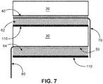
- Fig. 7 shows an example of this implementation. It must be noted however, that for flat panel applications, the bottom back-illumination may already be available. In this case the stack can again consist of a single glass plate sandwiched between both layers, however only serving the top layer.
- the inner glass plate is equipped with a reflector 110 on its bottom side, maximized the use of light and helping prevent light crosstalk across layers.
- the embodiment shown in Fig. 7 is just one of a number of possible arrangements.
- the top layer can be a back-illuminated BIP PDA and the bottom layer can be a front-illuminated FIP.
- the top layer can be a FIP, with the bottom layer a BIP.
- both layers can be BIP or both layers can be FIP.
- any of the arrangements of layers discussed above with respect to Fig. 7 can be reversed, in that rather than X-rays coming from top of the figures, X-rays can come from the bottom
- the flex foil electrodes 70, 80 shown in the embodiment of Fig. 3 and indeed in the embodiment shown in Fig. 7 can carry supply voltages to the LEDs of the glass plate as well as provide voltages to the photodiode arrays.
- the flex foil electrodes for the x-ray detector as shown in Fig. 4 are now positioned between the photodiode arrays and the scintillators, and as such a different technique is required to bias the light emitting glass plate. There are several mechanisms how this can be accomplished:
- the Photodiode arrays can have a substrate (also called bulk) contact on top. That is, the substrate (bottom side) of the photodiode can be biased to a certain potential from a top contact. The other photodiode layer can then to be biased to a different potential sufficient to drive the LEDs associated with the glass plate. That is, the bottom side of the photodiode arrays can provide the biasing.
- the photodiode have TSV (through silicon vias) contacts bringing a dedicated bias voltage from top to bottom (mirrored for Fig. 4 ) and give access to the glass plate.
- TSV through silicon vias
- the flex foil (top layer) can make contact to the side of the plate. This is particularly suited when LEDs are placed on the side of the glass plate, but it is not restricted to this embodiment.
- the glass plate can have a dedicated flex foil coming out of a 3 rd side (or two sides).
- an embodiment of the X-ray detector can in effect be a combination of the embodiments shown in Fig. 3 and Fig. 4 is in principle possible.
- the top layer can be back-illuminated and provide the bias for the plate through the flex foil only from one side.
- the bottom layer can then be any type of photodiode with no need for contacting the plate.
- the flex foils are therefore acting as an interconnect to the photodiode electrodes and can also provide the bias for the light emitting glass plate.
- the X-ray detector is used in CT applications, where the full detector is composed of tiles, i.e. the detector consists of smaller elements arranged adjacent to each other resulting on a large area detector.
- the "flex foil" can be in the form of a TFT panel (Thin-Film transistor, flex or otherwise) which also provides the front-end read-out for the photodiodes.
- the TFT can then connect to line amplifiers and ADC on one or more sides.
- the light emitting layer in the form of a glass plate with LEDs has been described, where it was mentioned that polymer rather than glass could be utilized.
- the light emitting layer can be in the form of a thin electroluminescent layer, such as an organic light emitting diode OLED layer.
Abstract
The present invention relates to an X-ray detector (10), comprising: a first scintillator (20); a second scintillator (30); a first photodiode array (40); a second photodiode array (50); and at least one layer (60). The first scintillator is configured to absorb X-rays from an X-ray pulse and emit light. The first photodiode array is positioned adjacent to the first scintillator. The first photodiode array is configured to detect at least some of the light emitted by the first scintillator. The second scintillator is configured to absorb X-rays from the X-ray pulse and emit light. The second photodiode array is positioned adjacent to the second scintillator. The second photodiode array is configured to detect at least some of the light emitted by the second scintillator. The at least one layer is configured to emit radiation. The at least one layer is configured such that at least some of the emitted radiation irradiates the first photodiode array and at least some of the emitted radiation irradiates the second photodiode array.
Description
- The present invention relates to an X-ray detector, and to an X-ray detector system.
- Specialized X-ray detectors for spectral energy computer tomography and/or X-ray applications, comprising two or more scintillator layers and associated photo diode arrays, are very expensive. Low-cost photodiodes, for example based on an organic layer - OPD - or amorphous silicon (a-Si), have a relatively high defect density in the bulk, where charge can be trapped at defect sites and released at a later time. Because of such an issue leading to image artefacts, these detectors cannot find utility in these specialized applications.
- There is a need to address this issue.
- It would be advantageous to have an ability to utilize low-cost photodiodes in specialized multiple layer X-ray detectors. The object of the present invention is solved with the subject matter of the independent claims, wherein further embodiments are incorporated in the dependent claims. It should be noted that the following described aspects and examples of the invention apply also to the X-ray detector and to the X-ray detector system.
- In a first aspect, there is provided an X-ray detector, comprising:
- a first scintillator;
- a second scintillator;
- a first photodiode array;
- a second photodiode array; and
- at least one layer.
- The first scintillator is configured to absorb X-rays from an X-ray pulse and (in response thereto) to emit light. The first photodiode array is positioned adjacent to the first scintillator. The first photodiode array is configured to detect at least some of the light emitted by the first scintillator. The second scintillator is configured to absorb X-rays from the X-ray pulse and (in response thereto) to emit light. The second photodiode array is positioned adjacent to the second scintillator. The second photodiode array is configured to detect at least some of the light emitted by the second scintillator. The at least one layer is configured to emit radiation. The at least one layer is configured such that at least some of the emitted radiation irradiates the first photodiode array and at least some of the emitted radiation irradiates the second photodiode array.
- In this manner, a dual layer detector for example for computed tomography dual energy applications, can utilize low-cost photodiodes (based on for example an organic layer OPD or a-Si). This is because although these low-cost photodiodes have a relatively high defect density in the bulk, a light emitting layer is provided that can for example emit visible and ultraviolet light below 750nm to fill defect sites, or infrared radiation for example above 750nm to fill traps within the bandgap. This means that problems such as a change in effective gain (or detective efficiency) and/or a change in the step response for such low-cost detectors is mitigated.
- The first photodiode array being positioned adjacent to the first scintillator does not preclude another element of the X-ray detector being between the first photodiode array and the first scintillator.
- The second photodiode array being positioned adjacent to the second scintillator does not preclude another element of the X-ray detector being between the second photodiode array and the second scintillator.
- In an example, the at least one layer is configured to emit radiation at infrared wavelengths, and/or the at least one layer is configured to emit radiation at visible and/or the at least one layer is configured to emit radiation at ultraviolet wavelengths.
- In an example, the at least one layer is positioned between the first photodiode and the second photodiode.
- In this manner, only one light emitting layer is required, that can emit radiation in one direction to radiate the first photodiode and emit radiation in the counter direction to radiate the second photodiode.
- The at least one layer being positioned between the first photodiode and the second photodiode does not preclude another element of the X-ray detector being between the at least one layer and the first photodiode.
- The at least one layer being positioned between the first photodiode and the second photodiode does not preclude another element of the X-ray detector being between the at least one layer and the second photodiode.
- In an example, the at least one layer is configured such that a transmission of the at least one layer in a direction from the first photodiode array to the second photodiode array for light emitted by the first scintillator and/or for light emitted by the second scintillator is less than 10%, preferable less than 5%, more preferably less than 1%.
- This means that crosstalk from one scintillator to the other scintillator is minimized, because radiation emitted by a scintillator cannot (or at least the majority of radiation cannot) cross the layer and be collected by the photodiode array associated with the other scintillator.
- In an example, a first layer of the at least one layer is positioned below the first photodiode and a second layer of the at least one layer is positioned below the second photodiode.
- Here, below means on a side of the first photodiode away from the source of X-rays.
- In this manner, crosstalk can be completely eliminated because one layer is positioned between the two scintillators, and a bottom surface of that layer can be made as a reflector for example or radiation blocker. This reflector or radiation blocker stops radiation from one scintillator being detected by the photodiode array associated with the other scintillator. If reflectors are used then these can be used for both layers and maximize the amount of radiation emitted in the direction of the associated photodiode array for that layer. The first layer of the at least one layer being positioned below the first photodiode does not preclude another element of the X-ray detector being between the first layer and the first photodiode.
- The second layer of the at least one layer being positioned below the second photodiode does not preclude another element of the X-ray detector being between the second layer and the second photodiode.
- In an example, the at least one layer comprises at least one glass or polymer plate. At least one light source is configured to generate the radiation that is emitted by the at least one layer.
- In an example, the at least one light source can be at least one LED.
- In an example, the at least one light source is positioned proximate to at least one edge of the at least one layer.
- This means, that X-rays can interact with both scintillators without having light sources such as LEDs in the X-ray path.
- In an example, the at least one edge of the at least one layer is mirrored.
- In this manner, light escaping from one or more sides of the at least one layer is minimized, thereby maximizing light emitted towards photodiodes.
- Here mirrored means that the at least one edge can be supplied with a reflective coating, or given a mirror finish.
- In an example, at least one face of the at least one layer substantially perpendicular to the at least one edge is roughened.
- In this way, light coupling out of the surface or surfaces of the at least one layer towards photodiodes can be enhanced.
- In an example, the at least one LED is integrated into the at least one layer.
- In an example, the at least one layer comprises at least one OLED layer.
- In an example, a first surface of the first photodiode array faces the first scintillator and a second surface of the first photodiode array faces away from the first scintillator and a first surface of the second photodiode array faces the second surface of the first photodiode array. A first electrode is in contact with the second surface of the first photodiode array and a second electrode is in contact with the first surface of the second photodiode array.
- In this manner, electrodes that are used as part of the biasing potential for the photodiode arrays can also be used as part of the power supply for light emitting means such as LEDs associated with the at least one layer.
- In an example, the first electrode and second electrode are in contact with the at least one layer.
- In a second aspect, there is provided an X-ray detector system, comprising an X-ray detector according to the first aspect; and a processing unit configured to control the X-ray detector such that the at least one layer does not emit radiation when the X-ray source is emitting X-rays.
- In a third aspect, there is provided an X-ray detector system, comprising an X-ray source; and an X-ray detector according to the first aspect. Optionally, the X-ray detector system may also include the processing unit configured to control the X-ray detector such that the at least one layer does not emit radiation when the X-ray source is emitting X-rays.
- Thus, the light emitting layer can operate continuously, however the photodiode arrays can generate an offset current when the x-ray sources operating that can be considered as a source of noise, however now the layer operates to mitigate the effect of defects only when the x-ray source is not operating. In other words, the layer(s) does not provide illumination to the photodiode arrays during x-ray radiation, and can otherwise be permanently on.
- Advantageously, the benefits provided by any of the above aspects equally apply to all of the other aspects and vice versa.
- The above aspects and examples will become apparent from and be elucidated with reference to the embodiments described hereinafter.
- Exemplary embodiments will be described in the following with reference to the following drawing:
-
Fig. 1 shows a schematic set up of an example of an X-ray detector; -
Fig. 2 shows a schematic set up of an example of an X-ray detector system; -
Fig. 3 shows a schematic set up of an example of an X-ray detector; -
Fig. 4 shows a schematic set up of an example of an X-ray detector; -
Fig. 5 shows a schematic set up of an example of a light emitting layer of an example of an X-ray detector; -
Fig. 6 shows a schematic set up of an example of a light emitting layer of an example of an X-ray detector; and -
Fig. 7 shows a schematic set up of an example of an X-ray detector. -
Fig. 1 shows an example of anX-ray detector 10. The X-ray detector comprises afirst scintillator 20, asecond scintillator 30, afirst photodiode array 40, asecond photodiode array 50, and at least onelayer 60. The first scintillator is configured to absorb X-rays from an X-ray pulse and emit light. The first photodiode array is positioned adjacent to the first scintillator. The first photodiode array is configured to detect at least some of the light emitted by the first scintillator. The second scintillator is configured to absorb X-rays from the X-ray pulse and emit light. The second photodiode array is positioned adjacent to the second scintillator. The second photodiode array is configured to detect at least some of the light emitted by the second scintillator. The at least one layer is configured to emit radiation. The at least one layer is configured such that at least some of the emitted radiation from the at least one layer irradiates the first photodiode array and at least some of the emitted radiation from the at least one layer irradiates the second photodiode array. - In an example, the at least one layer has a thickness no greater than 0.5mm.
- In an example, the at least one layer has a thickness no greater than 0.3mm.
- In an example, the at least one layer comprises at least one light plate.
- According to an example, the at least one layer is configured to emit radiation at infrared wavelengths, and/or the at least one layer is configured to emit radiation at visible and/or the at least one layer is configured to emit radiation at ultraviolet wavelengths.
- In an example, the visible and/or UV radiation is below 750nm.
- In an example, the infrared radiation is above 750nm.
- The skilled person would appreciate that these number are merely representative, thus for example visible and ultraviolet can in some cases be considered to be below 800nm, and infrared can in some case be considered to above 800nm or indeed above 900nm.
- According to an example, the at least one layer is positioned between the first photodiode and the second photodiode.
- According to an example, the at least one layer is configured such that a transmission of the at least one layer in a direction from the first photodiode array to the second photodiode array for light emitted by the first scintillator is less than 10%, preferable less than 5%, more preferably less than 1%.
- According to an example, the at least one layer is configured such that a transmission of the at least one layer in a direction from the second photodiode array to the first photodiode array for light emitted by the second scintillator is less than 10%, preferable less than 5%, more preferably less than 1%.
- According to an example, a
first layer 62 of the at least one layer is positioned below the first photodiode and asecond layer 64 of the at least one layer is positioned below the second photodiode.Fig. 7 described below shows a possible embodiment of this example. - According to an example, the at least one layer comprises at least one glass or polymer plate, and at least one
light source 90 is configured to generate the radiation that is emitted by the at least one layer. - The at least one light source can be at least one light emitting diode (LED).
- According to an example, the at least one light source is positioned proximate to at least one edge of the at least one layer.
- The at least one light source, such as one or more LEDs, can be external to a layer, transmitting light into layer, or can be embedded within the layer near to the edge of the layer.
- According to an example, the light sources (e.g. LEDs) are within the layer and at least one edge of the at least one layer is mirrored 100.
- However, light sources (e.g. LEDs) can be external to a layer injecting light into the layer to an edge that is not mirrored, whilst other edges of the layer can be mirrored.
- According to an example, at least one face of the at least one layer substantially perpendicular to the at least one edge is roughened.
- According to an example, the at least one light source such as at least one LED is integrated into the at least one layer.
- According to an example, the at least one layer comprises at least one organic light emitting diode (OLED) layer.
- According to an example, a first surface of the first photodiode array faces the first scintillator and a second surface of the first photodiode array faces away from the first scintillator and a first surface of the second photodiode array faces the second surface of the first photodiode array, and wherein a first electrode (70) is in contact with the second surface of the first photodiode array and a second electrode (80) is in contact with the first surface of the second photodiode array.
- According to an example, the first electrode and second electrode are in contact with the at least one layer.
-
Fig. 2 shows an example of anX-ray detector system 200. The X-ray detector system comprises anX-ray source 210, and anX-ray detector 10 as described above with respect toFig. 1 . - According to an example, the
X-ray detector system 200 comprises aprocessing unit 220. The processing unit is configured to control the X-ray detector such that the at least one layer does not emit radiation when the X-ray source is emitting X-rays. - Thus for example, LEDs producing the light that is emitted by the at least one layer are controlled so as not to emit light when the X-ray source is emitting X-rays.
- The X-ray detector and X-ray detector system are now described in further detail relating to specific embodiments, where reference is made to
Figs. 3-7 . - Low cost photodiodes (based on organic layer -OPD- or a-Si) can now be used to replace expensive photodiodes in CT, through the special x-ray detector configuration described here. Thus, OPDs can now also considered for next generation dual-layer flat X-ray detectors. Up until now, these types of photodiodes arrays (PDA), albeit cost effective, have suffered from a number of artifacts which have hindered their adoption in these applications, particularly that for CT.
- To set the scene, relating to the problem addressed by the current x-ray detector configuration, the following provides further details relating to the problems associated with low-cost photodiodes arrays. The most relevant non-ideal behavior relates to the PDA temporal characteristics. The effective gain (or detective efficiency) and the step response may appear to change over time due to charge trapping in the active area. Since these photodiodes can have a relatively high defect density in the bulk, charge can be trapped at the defect sites and only released at a comparatively very long time scale. This can cause ghosting-like artefacts, but also image artefacts, e.g. band artefacts in CT. Methods to counteract the temporal artefacts due to charge trapping are known, e.g. switching off bias; or short forward biasing intervals. Solutions for dual-layer detector applications involving bias light / backlighting have however up until now been lacking.
- As discussed above, and providing more detail below, the present detector addresses this through a special arrangement of layers with one or more light emitting layers within detector arrangement used for "backlighting" of low-cost photodiodes used to detect radiation emitted from scintillators, where such low-cost photodiodes can be based on OPD or a-Si.
- The inventors realized that by using a light wavelength with energy above the material bandgap (i.e. red light below 800 nm, the defect sites in the photodiodes used within the x-ray detector can be filled prior to X-ray illumination. Having filled the traps, it implies that no further trapping may occur and no changes of the detection efficiency may be perceived during the X-ray illumination. Furthermore, by doing so before every X-ray scan, it ensures that the same initial conditions are met for every image task. Furthermore, the inventors realized that illumination in the infrared sub-band (e.g. IR > 900 nm) can also be used in order to fill traps within the bandgap.
- It is however to be noted, that such pulsed operation of light emission within the new detector is not essential, and continuous backlight illumination can be considered. Here, the red and/or infrared illumination can remain on all the time. This can however also mean that the photodiode generates an offset current corresponding to the responsivity to the light, which may be considered as a source of noise. In this event, the pulsed backlight illumination as discussed above finds utility, where the illumination is switched off during the X-ray irradiation, and otherwise permanently on.
-
Fig. 3 shows an example of the new type ofX-ray detector 10. The X-ray detector has atop layer scintillator 20, with a low-cost photodiode array 40 positioned adjacent to the top layer scintillator to detect radiation emitted from the scintillator resulting from the absorption of x-rays. The X-ray detector also has a bottom therescintillator 30, with another low-cost photodiode array 50 positioned adjacent to the bottom there scintillator detect radiation emitted from the scintillator resulting from the absorption of x-rays. Aglass plate 60 is introduced between both photodiode arrays, which acts as alight emitting layer 60. The plate has integratedLEDs 90 and it serves as a diffusion plate such that the two PDA arrays are homogenously illuminated, thereby filling the defect sites and/or filling traps depending upon the wavelength of emission of the LEDs as discussed above. Other materials alternative to glass can be used for example, thick polymers, PMMA, etc. Thus theglass plate 60 acts as a mechanical support and infrared and/or red light, diffusion based light emitting layer. - In
Fig. 3 theelectrodes Fig. 3 , the PDAs can be taken to be "back" illuminated by the light emitting layer 60 (for light proceeding from the scintillator). Alternatively, the flex foil may be on top of the PDA (front-illuminated type) and it only requires being optically transparent (e.g. ITO routing). In this alternative configuration (seeFig. 4 ), the glass plate is in direct contact with the PDA array. - A benefit of the embodiment shown in
Fig. 3 , is that the flex substrates (flex foil electrodes) can carry the supply voltage to the LEDs of the glass plate as well as provide bias voltages to the PDAs. Since the glass plate is "sandwiched" between two flex foils, each foil can carry one of the supplies, e.g. common cathode top and common anode bottom, or vice versa. - The glass can cause some undesirable X-ray absorption. It is therefore of benefit that the glass substrate be kept as thin as possible. Ideally, it should not be thicker than 0.5 mm, preferably thinner than 0.3 mm.
- Regarding, the embodiments shown in
Figs 3 and 4 , due to the almost transparent nature of the PDA (particularly OPD), light crosstalk can occur across both scintillator layers, deteriorating the energy separation of the dual layer detector. To address this, the glass surfaces can be treated to have a transmission, across the interface, of for example only 10%. The remaining light can be reflected and/or absorbed. With a 10 % transmission on each glass surface/interface, the crosstalk across both layers is constrained to well below 1%, since light trying to travel from one scintillator to the other scintillator's photodiode will have to cross two successive interfaces with 10% transmission. The LED array providing radiation for the glass light emitting layer, in such a situation may need to provide more light to compensate for the lack of transmission at the exit surfaces of the glass layer. The flex foil electrodes for as shown inFig. 4 are now positioned between the photodiode arrays and the scintillators. -
Figs 5 and 6 show examples of exemplary glass plates. Preferably all or most of the edge sides of the glass plates are cladded with a reflective material such that the light emitted by both top and bottom surfaces is maximized. Thus, the glass plate has reflective or mirrorededges 100 for example a mirror or TiO2 (from the inner side). - In the embodiment shown in
Fig. 5 , theLED diodes 90 are integrated into the glass plate. In this embodiment, theelectrodes - In the embodiment shown in
Fig. 6 , theLED diodes 90 are placed only at the sides of the glass plate to maximize the edge mirror coverage, i.e. reflected light on the edges is not absorbed by the LED array in the glass volume. In this case the LEDs are also not in the X-ray path for the lower layer detector. The top and bottom surface of the glass layer can be roughened to enhance out-coupling of light from the LEDs via scattering. The roughening of surfaces can also apply to the embodiment shown inFig. 5 . - In flat detectors, the existing glass plate can be used to couple light from the sides. The bottom surface of the plate may be treated to increase light scatter and produce a homogenous light distribution across the detector.
- In the above embodiments the glass plate is placed in between and serves both photo diode layers. Alternatively, each photodiode layer may have its own light emitting layer or plate. In this case, crosstalk across layers can be minimized or even completely eliminated, at the expense of a slightly more complicated stack.
Fig. 7 shows an example of this implementation. It must be noted however, that for flat panel applications, the bottom back-illumination may already be available. In this case the stack can again consist of a single glass plate sandwiched between both layers, however only serving the top layer. As it can be seen inFig. 7 , now the inner glass plate is equipped with areflector 110 on its bottom side, maximized the use of light and helping prevent light crosstalk across layers. However, rather than a mirror this layer could just be a radiation blocking layer for UV/visible/infrared, whilst being not overly attenuating to x-rays. It is to be noted that the embodiment shown inFig. 7 is just one of a number of possible arrangements. For example the top layer can be a back-illuminated BIP PDA and the bottom layer can be a front-illuminated FIP. However, the top layer can be a FIP, with the bottom layer a BIP. However, both layers can be BIP or both layers can be FIP. Also, any of the arrangements of layers discussed above with respect toFig. 7 can be reversed, in that rather than X-rays coming from top of the figures, X-rays can come from the bottom - As discussed above, the
flex foil electrodes Fig. 3 and indeed in the embodiment shown inFig. 7 can carry supply voltages to the LEDs of the glass plate as well as provide voltages to the photodiode arrays. The flex foil electrodes for the x-ray detector as shown inFig. 4 are now positioned between the photodiode arrays and the scintillators, and as such a different technique is required to bias the light emitting glass plate. There are several mechanisms how this can be accomplished: - The Photodiode arrays can have a substrate (also called bulk) contact on top. That is, the substrate (bottom side) of the photodiode can be biased to a certain potential from a top contact. The other photodiode layer can then to be biased to a different potential sufficient to drive the LEDs associated with the glass plate. That is, the bottom side of the photodiode arrays can provide the biasing.
- The photodiode have TSV (through silicon vias) contacts bringing a dedicated bias voltage from top to bottom (mirrored for
Fig. 4 ) and give access to the glass plate. In this case, it can be sufficient that only one array provides both potentials to the plate, which is particularly suitable if the plate has contacts only on one side. (For the embedded LED case the contacts can be on both sides). Because the photodiode are typically very thin, TSVs are compatible. - The flex foil (top layer) can make contact to the side of the plate. This is particularly suited when LEDs are placed on the side of the glass plate, but it is not restricted to this embodiment.
- The glass plate can have a dedicated flex foil coming out of a 3rd side (or two sides).
- It is also to be noted that an embodiment of the X-ray detector can in effect be a combination of the embodiments shown in
Fig. 3 and Fig. 4 is in principle possible. In this combined embodiment, the top layer can be back-illuminated and provide the bias for the plate through the flex foil only from one side. The bottom layer can then be any type of photodiode with no need for contacting the plate. - For the embodiments discussed above, the flex foils are therefore acting as an interconnect to the photodiode electrodes and can also provide the bias for the light emitting glass plate. This applies for the case where the X-ray detector is used in CT applications, where the full detector is composed of tiles, i.e. the detector consists of smaller elements arranged adjacent to each other resulting on a large area detector. However, this also applies for X-ray detectors for other X-ray applications. In this latter case, large area devices find utility and the "flex foil" can be in the form of a TFT panel (Thin-Film transistor, flex or otherwise) which also provides the front-end read-out for the photodiodes. The TFT can then connect to line amplifiers and ADC on one or more sides.
- In the above discussion, light emitting layer in the form of a glass plate with LEDs has been described, where it was mentioned that polymer rather than glass could be utilized. However, the light emitting layer, can be in the form of a thin electroluminescent layer, such as an organic light emitting diode OLED layer.
- It has to be noted that embodiments of the invention are described with reference to different subject matters. In particular, some embodiments are described with reference to method type claims whereas other embodiments are described with reference to the device type claims. However, a person skilled in the art will gather from the above and the following description that, unless otherwise notified, in addition to any combination of features belonging to one type of subject matter also any combination between features relating to different subject matters is considered to be disclosed with this application. However, all features can be combined providing synergetic effects that are more than the simple summation of the features.
while the invention has been illustrated and described in detail in the drawings and foregoing description, such illustration and description are to be considered illustrative or exemplary and not restrictive. The invention is not limited to the disclosed embodiments. Other variations to the disclosed embodiments can be understood and effected by those skilled in the art in practicing a claimed invention, from a study of the drawings, the disclosure, and the dependent claims. - In the claims, the word "comprising" does not exclude other elements or steps, and the indefinite article "a" or "an" does not exclude a plurality. A single processor or other unit may fulfill the functions of several items re-cited in the claims. The mere fact that certain measures are re-cited in mutually different dependent claims does not indicate that a combination of these measures cannot be used to advantage. Any reference signs in the claims should not be construed as limiting the scope.
Claims (15)
- An X-ray detector (10), comprising:- a first scintillator (20);- a second scintillator (30);- a first photodiode array (40);- a second photodiode array (50); and- at least one layer (60);wherein, the first scintillator is configured to absorb X-rays from an X-ray pulse and to emit light;
wherein, the first photodiode array is positioned adjacent to the first scintillator;
wherein, the first photodiode array is configured to detect at least some of the light emitted by the first scintillator;
wherein, the second scintillator is configured to absorb X-rays from the X-ray pulse and to emit light;
wherein, the second photodiode array is positioned adjacent to the second scintillator;
wherein, the second photodiode array is configured to detect at least some of the light emitted by the second scintillator;
wherein, the at least one layer is configured to emit radiation; and
wherein, the at least one layer is configured such that at least some of the emitted radiation irradiates the first photodiode array and at least some of the emitted radiation irradiates the second photodiode array. - X-ray detector according to claim 1, wherein the at least one layer is configured to emit radiation at infrared wavelengths, and/or the at least one layer is configured to emit radiation at visible and/or ultraviolet wavelengths.
- X-ray detector according to any of claims 1-2, wherein the at least one layer is positioned between the first photodiode and the second photodiode.
- X-ray detector according to claim 3, wherein the at least one layer is configured such that a transmission of the at least one layer in a direction from the first photodiode array to the second photodiode array for light emitted by the first scintillator and/or for light emitted by the second scintillator is less than 10%, preferable less than 5%, more preferably less than 1%.
- X-ray detector according to any of claims 1-2, wherein a first layer (62) of the at least one layer is positioned below the first photodiode and a second layer (64) of the at least one layer is positioned below the second photodiode.
- X-ray detector according to any of claims 1-5, wherein the at least one layer comprises at least one glass or polymer plate, and wherein at least one light source (90) is configured to generate the radiation that is emitted by the at least one layer.
- X-ray detector according to claim 6, wherein the at least one light source is positioned proximate to at least one edge of the at least one layer.
- X-ray detector according to any of claims 6-7, wherein the at least one edge of the at least one layer is mirrored (100).
- X-ray detector according to any of claims 7-8, wherein at least one face of the at least one layer substantially perpendicular to the at least one edge is roughened.
- X-ray detector according to claim 6, wherein the at least one LED is integrated into the at least one layer.
- X-ray detector according to any of claims 1-5, wherein the at least one layer comprises at least one OLED layer.
- X-ray detector according to any of claims 1-11, wherein a first surface of the first photodiode array faces the first scintillator and a second surface of the first photodiode array faces away from the first scintillator and a first surface of the second photodiode array faces the second surface of the first photodiode array, and wherein a first electrode (70) is in contact with the second surface of the first photodiode array and a second electrode (80) is in contact with the first surface of the second photodiode array.
- X-ray detector according to claim 12, wherein the first electrode and second electrode are in contact with the at least one layer.
- X-ray detector system (200) for use with an X-ray source, comprising:- an X-ray detector (10) according to any of claims 1-13; and- a processing unit (220), wherein the processing unit is configured to control the X-ray detector such that the at least one layer does not emit radiation when the X-ray source is emitting X-rays.
- X-ray detector system (200), comprising:- an X-ray source (210); and- an X-ray detector (10) according to any of claims 1-14.
Priority Applications (6)
| Application Number | Priority Date | Filing Date | Title |
|---|---|---|---|
| EP19214388.1A EP3835829A1 (en) | 2019-12-09 | 2019-12-09 | X-ray detector |
| JP2022534465A JP2023503529A (en) | 2019-12-09 | 2020-12-02 | X-ray detector |
| EP20812379.4A EP4049065B1 (en) | 2019-12-09 | 2020-12-02 | X-ray detector |
| PCT/EP2020/084219 WO2021115865A1 (en) | 2019-12-09 | 2020-12-02 | X-ray detector |
| US17/780,500 US11662482B2 (en) | 2019-12-09 | 2020-12-02 | X-ray detector comprising at least one light emitting layer |
| CN202080085614.8A CN114846359B (en) | 2019-12-09 | 2020-12-02 | X-ray detector |
Applications Claiming Priority (1)
| Application Number | Priority Date | Filing Date | Title |
|---|---|---|---|
| EP19214388.1A EP3835829A1 (en) | 2019-12-09 | 2019-12-09 | X-ray detector |
Publications (1)
| Publication Number | Publication Date |
|---|---|
| EP3835829A1 true EP3835829A1 (en) | 2021-06-16 |
Family
ID=68835105
Family Applications (2)
| Application Number | Title | Priority Date | Filing Date |
|---|---|---|---|
| EP19214388.1A Withdrawn EP3835829A1 (en) | 2019-12-09 | 2019-12-09 | X-ray detector |
| EP20812379.4A Active EP4049065B1 (en) | 2019-12-09 | 2020-12-02 | X-ray detector |
Family Applications After (1)
| Application Number | Title | Priority Date | Filing Date |
|---|---|---|---|
| EP20812379.4A Active EP4049065B1 (en) | 2019-12-09 | 2020-12-02 | X-ray detector |
Country Status (5)
| Country | Link |
|---|---|
| US (1) | US11662482B2 (en) |
| EP (2) | EP3835829A1 (en) |
| JP (1) | JP2023503529A (en) |
| CN (1) | CN114846359B (en) |
| WO (1) | WO2021115865A1 (en) |
Citations (4)
| Publication number | Priority date | Publication date | Assignee | Title |
|---|---|---|---|---|
| US5025462A (en) * | 1989-06-21 | 1991-06-18 | Kabushiki Kaisha Toshiba | X-ray detector having function of compensating for sensitivity of scintillator |
| KR20080092393A (en) * | 2008-07-28 | 2008-10-15 | 시마쯔 코포레이션 | Radiation detector |
| WO2011135486A2 (en) * | 2010-04-26 | 2011-11-03 | Koninklijke Philips Electronics N.V. | X-ray detector with improved spatial gain uniformity and resolution and method of fabricating such x-ray detector |
| US20140339431A1 (en) * | 2013-05-15 | 2014-11-20 | Canon Kabushiki Kaisha | Detecting apparatus and detecting system |
Family Cites Families (55)
| Publication number | Priority date | Publication date | Assignee | Title |
|---|---|---|---|---|
| US4437006A (en) * | 1978-02-21 | 1984-03-13 | Scientific Measurement Systems, Inc. | Method and apparatus for measuring radiation in computer-assisted tomography and radiographic applications |
| US4511799A (en) * | 1982-12-10 | 1985-04-16 | American Science And Engineering, Inc. | Dual energy imaging |
| US6031892A (en) * | 1989-12-05 | 2000-02-29 | University Of Massachusetts Medical Center | System for quantitative radiographic imaging |
| US5548123A (en) * | 1994-12-06 | 1996-08-20 | Regents Of The University Of California | High resolution, multiple-energy linear sweep detector for x-ray imaging |
| DE10139234A1 (en) * | 2001-08-09 | 2003-02-27 | Philips Corp Intellectual Pty | X-ray detector with heating device |
| JP2006524327A (en) * | 2003-04-24 | 2006-10-26 | コーニンクレッカ フィリップス エレクトロニクス エヌ ヴィ | Detector element for spatially resolved detection of gamma rays |
| US20050135535A1 (en) * | 2003-06-05 | 2005-06-23 | Neutron Sciences, Inc. | Neutron detector using neutron absorbing scintillating particulates in plastic |
| US7286640B2 (en) * | 2004-04-09 | 2007-10-23 | Xradia, Inc. | Dual-band detector system for x-ray imaging of biological samples |
| US7671342B2 (en) * | 2005-01-11 | 2010-03-02 | Siemens Medical Solutions Usa, Inc. | Multi-layer detector and method for imaging |
| EP1875273B1 (en) * | 2005-04-22 | 2011-11-16 | Koninklijke Philips Electronics N.V. | Pet/mr scanner with time-of-flight capability |
| WO2006114716A2 (en) * | 2005-04-26 | 2006-11-02 | Koninklijke Philips Electronics, N.V. | Double decker detector for spectral ct |
| CN103760588B (en) * | 2005-04-26 | 2018-05-22 | 皇家飞利浦电子股份有限公司 | The detector array of spectral CT |
| US7263165B2 (en) * | 2005-07-14 | 2007-08-28 | Siemens Medical Solutions Usa, Inc. | Flat panel detector with KV/MV integration |
| US7696481B2 (en) * | 2005-11-22 | 2010-04-13 | General Electric Company | Multi-layered detector system for high resolution computed tomography |
| US7388208B2 (en) * | 2006-01-11 | 2008-06-17 | Ruvin Deych | Dual energy x-ray detector |
| US7375341B1 (en) * | 2006-05-12 | 2008-05-20 | Radiation Monitoring Devices, Inc. | Flexible scintillator and related methods |
| US7834321B2 (en) * | 2006-07-14 | 2010-11-16 | Carestream Health, Inc. | Apparatus for asymmetric dual-screen digital radiography |
| RU2472180C2 (en) | 2007-04-12 | 2013-01-10 | Конинклейке Филипс Электроникс Н.В. | Reducing trap effects in scintillator by using secondary radiation |
| JP5124226B2 (en) * | 2007-10-01 | 2013-01-23 | 浜松ホトニクス株式会社 | Radiation detector |
| JP5142943B2 (en) | 2007-11-05 | 2013-02-13 | キヤノン株式会社 | Radiation detection device manufacturing method, radiation detection device and radiation imaging system |
| BRPI0910206A2 (en) * | 2008-06-30 | 2015-09-29 | Koninkl Philips Electronics Nv | computed tomography imaging system and method |
| KR101504491B1 (en) * | 2008-12-02 | 2015-03-23 | 삼성전자주식회사 | Apparatus for obtaining x-ray image, method for obtaining x-ray, sensor, imaging device |
| US8653471B2 (en) * | 2009-03-26 | 2014-02-18 | Koninklijke Philips N. V. | Spectral imaging |
| CA2766485C (en) * | 2009-07-16 | 2017-07-25 | Karim S. Karim | Multi-layer flat panel x-ray detector |
| JP5457118B2 (en) * | 2009-09-18 | 2014-04-02 | 浜松ホトニクス株式会社 | Radiation detector |
| JP5295915B2 (en) * | 2009-09-18 | 2013-09-18 | 浜松ホトニクス株式会社 | Radiation detector |
| US8729478B2 (en) * | 2010-06-09 | 2014-05-20 | Carestream Health, Inc. | Dual screen radiographic detector with improved spatial sampling |
| US8466421B2 (en) * | 2010-07-30 | 2013-06-18 | Varian Medical Systems Inc. | Radiation detector with multiple operating schemes |
| RU2581721C2 (en) * | 2010-12-13 | 2016-04-20 | Конинклейке Филипс Электроникс Н.В. | Radiation detector with photodetectors |
| US8772728B2 (en) * | 2010-12-31 | 2014-07-08 | Carestream Health, Inc. | Apparatus and methods for high performance radiographic imaging array including reflective capability |
| JP5117584B2 (en) * | 2011-01-25 | 2013-01-16 | 浜松ホトニクス株式会社 | Scintillator plate |
| WO2012109273A2 (en) | 2011-02-08 | 2012-08-16 | Rapiscan Systems, Inc. | Covert surveillance using multi-modality sensing |
| JP5604326B2 (en) * | 2011-02-14 | 2014-10-08 | 富士フイルム株式会社 | Radiation image detection apparatus and manufacturing method thereof |
| JP2012233781A (en) | 2011-04-28 | 2012-11-29 | Fujifilm Corp | Radiation image detector and radiographic device |
| TWI455297B (en) * | 2011-07-25 | 2014-10-01 | Innolux Corp | X-ray image sensing device and x-ray image sensing module |
| JP2013029384A (en) * | 2011-07-27 | 2013-02-07 | Canon Inc | Radiation detection device, manufacturing method thereof, and radiation detection system |
| US9012857B2 (en) * | 2012-05-07 | 2015-04-21 | Koninklijke Philips N.V. | Multi-layer horizontal computed tomography (CT) detector array with at least one thin photosensor array layer disposed between at least two scintillator array layers |
| JP6310703B2 (en) | 2014-01-21 | 2018-04-11 | 株式会社日立製作所 | Radiation detector and X-ray CT apparatus using the same |
| EP3137924A1 (en) * | 2014-04-30 | 2017-03-08 | Analogic Corporation | Detector array for imaging modality |
| US10234572B2 (en) * | 2014-07-25 | 2019-03-19 | The Regents Of The University Of California | Multiple spatial resolution scintillation detectors |
| US11156727B2 (en) * | 2015-10-02 | 2021-10-26 | Varian Medical Systems, Inc. | High DQE imaging device |
| WO2017116392A1 (en) | 2015-12-28 | 2017-07-06 | Analogic Corporation | Detector array for radiation imaging modality |
| CN109891269B (en) * | 2016-10-26 | 2023-11-10 | 皇家飞利浦有限公司 | Radiation detector scintillator with integral via interconnect |
| CN110168406A (en) * | 2017-01-02 | 2019-08-23 | 皇家飞利浦有限公司 | X-ray detector and x-ray imaging device |
| US11000701B2 (en) * | 2017-08-01 | 2021-05-11 | Varex Imaging Corporation | Dual-layer detector for soft tissue motion tracking |
| JP6991835B2 (en) * | 2017-11-10 | 2022-01-13 | キヤノン株式会社 | Radiation imaging device and radiation imaging system |
| US11346962B2 (en) * | 2017-11-17 | 2022-05-31 | Korea University Research And Business Foundation | Radiation detector for detecting radiation and identifying type thereof |
| EP3495849A1 (en) * | 2017-12-11 | 2019-06-12 | Koninklijke Philips N.V. | Multilayer pixelated scintillator with enlarged fill factor |
| EP3505969A1 (en) * | 2018-01-02 | 2019-07-03 | Koninklijke Philips N.V. | Detector for x-ray imaging |
| JP6932095B2 (en) * | 2018-03-06 | 2021-09-08 | 富士フイルム株式会社 | Radiation image detector |
| JP6987674B2 (en) * | 2018-03-06 | 2022-01-05 | 富士フイルム株式会社 | Radiation image detection device |
| JP6869914B2 (en) * | 2018-03-06 | 2021-05-12 | 富士フイルム株式会社 | Radiation image detector |
| JP2019152595A (en) * | 2018-03-06 | 2019-09-12 | 富士フイルム株式会社 | Radiation image detector |
| US10444378B1 (en) * | 2018-04-27 | 2019-10-15 | Varian Medical Systems, Inc. | Imaging devices |
| US11016202B2 (en) * | 2018-04-26 | 2021-05-25 | Varian Medical Systems, Inc. | Imaging devices |
-
2019
- 2019-12-09 EP EP19214388.1A patent/EP3835829A1/en not_active Withdrawn
-
2020
- 2020-12-02 EP EP20812379.4A patent/EP4049065B1/en active Active
- 2020-12-02 US US17/780,500 patent/US11662482B2/en active Active
- 2020-12-02 WO PCT/EP2020/084219 patent/WO2021115865A1/en unknown
- 2020-12-02 JP JP2022534465A patent/JP2023503529A/en active Pending
- 2020-12-02 CN CN202080085614.8A patent/CN114846359B/en active Active
Patent Citations (4)
| Publication number | Priority date | Publication date | Assignee | Title |
|---|---|---|---|---|
| US5025462A (en) * | 1989-06-21 | 1991-06-18 | Kabushiki Kaisha Toshiba | X-ray detector having function of compensating for sensitivity of scintillator |
| KR20080092393A (en) * | 2008-07-28 | 2008-10-15 | 시마쯔 코포레이션 | Radiation detector |
| WO2011135486A2 (en) * | 2010-04-26 | 2011-11-03 | Koninklijke Philips Electronics N.V. | X-ray detector with improved spatial gain uniformity and resolution and method of fabricating such x-ray detector |
| US20140339431A1 (en) * | 2013-05-15 | 2014-11-20 | Canon Kabushiki Kaisha | Detecting apparatus and detecting system |
Also Published As
| Publication number | Publication date |
|---|---|
| WO2021115865A1 (en) | 2021-06-17 |
| JP2023503529A (en) | 2023-01-30 |
| US20220365230A1 (en) | 2022-11-17 |
| US11662482B2 (en) | 2023-05-30 |
| EP4049065A1 (en) | 2022-08-31 |
| CN114846359B (en) | 2023-09-12 |
| CN114846359A (en) | 2022-08-02 |
| EP4049065B1 (en) | 2023-04-12 |
Similar Documents
| Publication | Publication Date | Title |
|---|---|---|
| JP5498982B2 (en) | Radiography equipment | |
| US8558184B2 (en) | Radiographic image capturing apparatus | |
| RU2561756C2 (en) | X-ray detector with increased amplification 3d uniformity and resolution and method of its configuration | |
| JP5653829B2 (en) | Radiographic apparatus, radiographic system, and radiographic method | |
| US20120126124A1 (en) | Radiographic image capturing apparatus | |
| JP2007155662A (en) | Radiation detector and radiation imaging system using the same | |
| CN103270595A (en) | Apparatus and methods for high performance radiographic imaging array including reflective capability | |
| US20120256095A1 (en) | Radiographic device and manufacturing method thereof | |
| KR20140067318A (en) | Digital x-ray image detector using multi-layered structure with surface light source | |
| JPWO2006046384A1 (en) | Radiation detector | |
| JP2012242355A (en) | Radiation detection device | |
| JP5624447B2 (en) | Radiation detection apparatus and scintillator panel manufacturing method | |
| JP2007147370A (en) | Radiation detection device and radiation imaging system | |
| WO2011148960A1 (en) | Radiological imaging device and method for assembling same | |
| EP4049065B1 (en) | X-ray detector | |
| CN113053966B (en) | Display panel, brightness compensation method and display device | |
| JP2004151007A (en) | Radiation detector | |
| JP2004239722A (en) | Radiation detector | |
| JP7198782B2 (en) | direct conversion radiation detection | |
| WO2012137425A1 (en) | X-ray detector | |
| JP2004163169A (en) | Radiation detector | |
| JP2012200373A (en) | Radiographic apparatus and its manufacturing method | |
| JP2011096794A (en) | Radiation image photographing device |
Legal Events
| Date | Code | Title | Description |
|---|---|---|---|
| PUAI | Public reference made under article 153(3) epc to a published international application that has entered the european phase |
Free format text: ORIGINAL CODE: 0009012 |
|
| STAA | Information on the status of an ep patent application or granted ep patent |
Free format text: STATUS: THE APPLICATION HAS BEEN PUBLISHED |
|
| AK | Designated contracting states |
Kind code of ref document: A1 Designated state(s): AL AT BE BG CH CY CZ DE DK EE ES FI FR GB GR HR HU IE IS IT LI LT LU LV MC MK MT NL NO PL PT RO RS SE SI SK SM TR |
|
| STAA | Information on the status of an ep patent application or granted ep patent |
Free format text: STATUS: THE APPLICATION IS DEEMED TO BE WITHDRAWN |
|
| 18D | Application deemed to be withdrawn |
Effective date: 20211217 |