JP6863505B2 - Diffusing member, laminate, set of diffusing member, LED backlight and display device - Google Patents
Diffusing member, laminate, set of diffusing member, LED backlight and display device Download PDFInfo
- Publication number
- JP6863505B2 JP6863505B2 JP2020078355A JP2020078355A JP6863505B2 JP 6863505 B2 JP6863505 B2 JP 6863505B2 JP 2020078355 A JP2020078355 A JP 2020078355A JP 2020078355 A JP2020078355 A JP 2020078355A JP 6863505 B2 JP6863505 B2 JP 6863505B2
- Authority
- JP
- Japan
- Prior art keywords
- layer
- light
- led
- diffraction grating
- resin
- Prior art date
- Legal status (The legal status is an assumption and is not a legal conclusion. Google has not performed a legal analysis and makes no representation as to the accuracy of the status listed.)
- Active
Links
Images


Description
本開示は、例えば直下型方式のLEDバックライトに用いられる拡散部材、積層体、および拡散部材のセット、ならびにそれを用いたLEDバックライトおよび表示装置に関する。 The present disclosure relates to, for example, a set of a diffusing member, a laminate, and a diffusing member used in a direct type LED backlight, and an LED backlight and a display device using the same.
近年、液晶表示装置等、LEDバックライトを光源として用いた表示装置が急速に普及している。 In recent years, display devices using an LED backlight as a light source, such as a liquid crystal display device, have rapidly become widespread.
ここで、LEDバックライトは、直下型方式とエッジライト型方式とに大別される。スマートフォン等の携帯端末等の中小型の表示装置においては、通常、エッジライト方式のLEDバックライトが用いられることが多いが、明るさ等の観点から、直下型方式のLEDバックライトを用いることが検討されている。一方、大画面液晶テレビ等の大型の表示装置においては、多くの場合、直下型方式のLEDバックライトが用いられる。 Here, the LED backlight is roughly classified into a direct type type and an edge light type type. In small and medium-sized display devices such as mobile terminals such as smartphones, an edge light type LED backlight is usually used, but from the viewpoint of brightness and the like, a direct type LED backlight may be used. It is being considered. On the other hand, in a large display device such as a large-screen liquid crystal television, a direct type LED backlight is often used.
直下型方式のLEDバックライトは、基板に複数のLED素子が配置された構成を有している。このような直下型方式のLEDバックライトでは、複数のLED素子を独立して制御することにより、表示画像の明暗に合わせてLEDバックライト各領域の明るさを調整する、いわゆるローカルディミングを実現することができる。これにより、表示装置の大幅なコントラスト向上および低消費電力化を図ることが可能となる。 The direct type LED backlight has a configuration in which a plurality of LED elements are arranged on a substrate. In such a direct type LED backlight, by independently controlling a plurality of LED elements, so-called local dimming is realized in which the brightness of each area of the LED backlight is adjusted according to the brightness of the displayed image. be able to. This makes it possible to significantly improve the contrast and reduce the power consumption of the display device.
直下型方式のLEDバックライトにおいては、輝度ムラの抑制等の観点から、LED素子の上方に拡散板を配置している。 In the direct type LED backlight, a diffuser plate is arranged above the LED element from the viewpoint of suppressing uneven brightness.
しかしながら、直下型方式のLEDバックライトでは、輝度ムラを抑制するために、LED素子と拡散板とを離して配置する必要がある。そのため、薄型化が困難である。特に、コストおよび消費電力を低減するためにLED素子の数を減らした場合、LED素子の配置間隔が広がるために輝度ムラが発生し易くなる。この場合、LED素子と拡散板との距離をより長くする必要があるので、薄型化がより困難となる。したがって、従来の直下型方式のLEDバックライトでは、輝度の均一化と薄型化とを同時に実現するのが困難であるという問題点がある。 However, in the direct type LED backlight, it is necessary to arrange the LED element and the diffuser plate apart from each other in order to suppress the uneven brightness. Therefore, it is difficult to reduce the thickness. In particular, when the number of LED elements is reduced in order to reduce cost and power consumption, uneven brightness is likely to occur because the arrangement intervals of the LED elements are widened. In this case, since it is necessary to increase the distance between the LED element and the diffuser plate, it becomes more difficult to reduce the thickness. Therefore, the conventional direct-type LED backlight has a problem that it is difficult to achieve uniform brightness and thinning at the same time.
また、輝度の面内均一性の向上のために、LED素子と拡散板との間に、さらに透過反射板を配置することが提案されている(例えば特許文献1参照)。透過反射板は、パターン状の反射部および透過部を有するものであり、より具体的には、LED素子の直上を反射部とし、LED素子の直上から周囲に向かって透過部が徐々に大きくなるようなパターンを有する。これにより、LED素子の直上の光を反射させて周囲に拡散し、周囲の透過部から出射させることができ、輝度の面内均一性を向上させることができる。 Further, in order to improve the in-plane uniformity of brightness, it has been proposed to further arrange a transmission reflector between the LED element and the diffuser (see, for example, Patent Document 1). The transmission reflector has a patterned reflection portion and a transmission portion. More specifically, the reflection portion is directly above the LED element, and the transmission portion gradually increases from directly above the LED element toward the periphery. It has such a pattern. As a result, the light directly above the LED element can be reflected and diffused to the surroundings and emitted from the surrounding transmitting portion, and the in-plane uniformity of the brightness can be improved.
しかしながら、このような透過反射板を用いる場合においても、輝度ムラを抑制するためには、LED素子と透過反射板とを離して配置する必要があるため、薄型化が困難である。また、透過反射板は、パターン状の反射部および透過部を有しており、反射部をLED素子の直上に配置することから、LED素子と透過反射板との位置合わせが必要になる。 However, even when such a transmissive reflector is used, it is difficult to reduce the thickness because it is necessary to dispose the LED element and the transmissive reflector separately in order to suppress the uneven brightness. Further, since the transmission reflector has a patterned reflection portion and a transmission portion and the reflection portion is arranged directly above the LED element, it is necessary to align the LED element and the transmission reflection plate.
また、輝度の均一化および薄型化のために、例えば特許文献2には、LED素子と拡散板との間に、入射する光の一部を反射し、一部を透過するハーフミラーを配置し、ハーフミラーとして、反射率が垂直入射よりも斜め入射の方が低いハーフミラーを用いることが提案されている。
Further, in order to make the brightness uniform and thin, for example, in
さらに、輝度の均一化のために、例えば特許文献3には、LED素子と拡散板との間に、光源からの光を透過回折し、光軸中心に射出される0より大きい透過回折光の強度と比較して、周辺部に射出される透過回折光の強度の方が強い環状の強度分布で透過回折光を射出する、バックライト用回折光学素子を配置することが提案されている。
Further, in order to make the brightness uniform, for example, in
本開示は、上記実情に鑑みてなされたものであり、輝度の面内均一性を向上させつつ、薄型化を図ることが可能な拡散部材、積層体、拡散部材のセット、LEDバックライトおよび表示装置を提供することを主目的とする。 The present disclosure has been made in view of the above circumstances, and is a diffusion member, a laminate, a set of diffusion members, an LED backlight and a display capable of reducing the thickness while improving the in-plane uniformity of brightness. The main purpose is to provide the device.
本発明者らは、上記課題を解決するため鋭意検討した結果、拡散部材として、光透過性および光拡散性を有する層と、反射率および透過率の入射角依存性を有する層とを組み合わせて用いることにより、輝度の面内均一性を向上させつつ、薄型化を図ることが可能であることを見出し、本発明を完成させるに至った。 As a result of diligent studies to solve the above problems, the present inventors have combined a layer having light transmittance and light diffusivity and a layer having reflectance and transmittance depending on the incident angle as a diffusion member. By using it, it has been found that it is possible to reduce the thickness while improving the in-plane uniformity of brightness, and the present invention has been completed.
すなわち、本開示の一実施形態は、第1層と、第2層とをこの順で有する拡散部材であって、上記第1層は、光透過性および光拡散性を有し、上記第2層は、上記第2層の上記第1層側の面に対する光の入射角の絶対値が小さくなるにつれて反射率が大きくなり、上記第2層の上記第1層側の面に対する光の入射角の絶対値が大きくなるにつれて透過率が大きくなる、拡散部材を提供する。 That is, one embodiment of the present disclosure is a diffusion member having a first layer and a second layer in this order, and the first layer has light transmittance and light diffusivity, and the second layer. The reflectance of the layer increases as the absolute value of the incident angle of light on the surface of the second layer on the first layer side decreases, and the incident angle of light on the surface of the second layer on the first layer side increases. Provided is a diffusing member in which the transmittance increases as the absolute value of is increased.
本開示の他の実施形態は、透過型回折格子またはマイクロレンズアレイと、誘電体多層膜とを有する、拡散部材を提供する。 Another embodiment of the present disclosure provides a diffusing member having a transmissive diffraction grating or microlens array and a dielectric multilayer film.
本開示の他の実施形態は、上述の拡散部材と、上記拡散部材の第1層側の面側に配置され、LED素子を封止するために用いられる封止材シートと、を備え、上記封止材シートは、熱可塑性樹脂を含有する封止材組成物から構成される、積層体を提供する。 Another embodiment of the present disclosure includes the above-mentioned diffusion member and a sealing material sheet arranged on the surface side of the first-layer side of the diffusion member and used for sealing the LED element. The encapsulant sheet provides a laminate composed of an encapsulant composition containing a thermoplastic resin.
本開示の他の実施形態は、上述の拡散部材と、上記拡散部材の透過型回折格子またはマイクロレンズアレイ側の面側に配置され、LED素子を封止するために用いられる封止材シートと、を備え、上記封止材シートは、熱可塑性樹脂を含有する封止材組成物から構成される、積層体を提供する。 Another embodiment of the present disclosure includes the above-mentioned diffusion member and a sealing material sheet arranged on the surface side of the diffusion member on the transmission type diffraction grating or microlens array side and used for sealing the LED element. The encapsulant sheet comprises, and provides a laminate composed of an encapsulant composition containing a thermoplastic resin.
本開示の他の実施形態は、第1層と、LED素子を封止するために用いられる封止材シートとを有する第1部材、および、第2層を有し、上記第1部材の上記第1層側の面に空隙部を介して配置されて用いられる第2部材を備え、上記第1層は、光透過性および光拡散性を有し、上記第2層は、上記第2層の上記第1層側の面に対する光の入射角の絶対値が小さくなるにつれて反射率が大きくなり、上記第2層の上記第1層側の面に対する光の入射角の絶対値が大きくなるにつれて透過率が大きくなり、上記封止材シートは、熱可塑性樹脂を含有する封止材組成物から構成される、拡散部材のセットを提供する。 Another embodiment of the present disclosure has a first member having a first layer and a sealing material sheet used for sealing the LED element, and a second layer, which is the above-mentioned first member. The surface on the first layer side is provided with a second member which is used by being arranged via a gap portion, the first layer has light transmittance and light diffusivity, and the second layer is the second layer. The reflectance increases as the absolute value of the incident angle of light with respect to the surface on the first layer side decreases, and as the absolute value of the incident angle of light with respect to the surface on the first layer side of the second layer increases. The transmittance is increased, and the encapsulant sheet provides a set of diffusion members composed of an encapsulant composition containing a thermoplastic resin.
本開示の他の実施形態は、支持基板の一方の面側に複数のLED素子が配置されたLED基板と、上記LED基板の上記LED素子側の面側に配置され、上記LED基板側から順に第1層および第2層を有する拡散部材とを備え、上記第1層は、光透過性および光拡散性を有し、上記第2層は、上記第2層の上記第1層側の面に対する光の入射角の絶対値が小さくなるにつれて反射率が大きくなり、上記第2層の上記第1層側の面に対する光の入射角の絶対値が大きくなるにつれて透過率が大きくなる、LEDバックライトを提供する。 In another embodiment of the present disclosure, an LED substrate in which a plurality of LED elements are arranged on one surface side of the support substrate and an LED substrate arranged on the surface side of the LED substrate on the LED element side are arranged in order from the LED substrate side. A diffusion member having a first layer and a second layer is provided, the first layer has light transmission and light diffusivity, and the second layer is a surface of the second layer on the first layer side. The reflectance increases as the absolute value of the incident angle of light with respect to the LED decreases, and the transmittance increases as the absolute value of the incident angle of light with respect to the surface of the second layer on the first layer side increases. Provide lights.
本開示の他の実施形態は、支持基板の一方の面側に複数のLED素子が配置されたLED基板と、上記LED基板の上記LED素子側の面側に配置された拡散部材と、を備え、上記拡散部材は、上記LED基板側から順に、透過型回折格子またはマイクロレンズアレイと、誘電体多層膜とを有する、LEDバックライトを提供する。 Another embodiment of the present disclosure includes an LED substrate in which a plurality of LED elements are arranged on one surface side of the support substrate, and a diffusion member arranged on the surface side of the LED substrate on the LED element side. The diffusion member provides an LED backlight having a transmission type diffraction lattice or a microlens array and a dielectric multilayer film in this order from the LED substrate side.
本開示は、表示パネルと、上記表示パネルの背面に配置された上述のLEDバックライトとを備える表示装置を提供する。 The present disclosure provides a display device including a display panel and the above-mentioned LED backlight arranged on the back surface of the display panel.
本開示は、輝度の面内均一性を向上させつつ、薄型化を図ることが可能な拡散部材、LEDバックライトおよび表示装置を提供することができるという効果を奏する。 The present disclosure has an effect that it is possible to provide a diffusion member, an LED backlight, and a display device capable of reducing the thickness while improving the in-plane uniformity of brightness.
以下、本開示の拡散部材、LEDバックライトおよび表示装置について説明する。但し、本開示は多くの異なる態様で実施することが可能であり、以下に例示する実施の態様の記載内容に限定して解釈されるものではない。また、図面は説明をより明確にするため、実施の態様に比べ、各部材の幅、厚さ、形状等について模式的に表される場合があるが、あくまで一例であって、本開示の解釈を限定するものではない。また、本明細書と各図において、既出の図に関して前述したものと同様の要素には、同一の符号を付して、詳細な説明を適宜省略することがある。 Hereinafter, the diffusion member, the LED backlight, and the display device of the present disclosure will be described. However, the present disclosure can be implemented in many different embodiments and is not construed as limited to the description of the embodiments exemplified below. Further, in order to clarify the description, the drawings may schematically represent the width, thickness, shape, etc. of each member as compared with the embodiment, but this is merely an example, and the interpretation of the present disclosure is given. Does not limit. Further, in the present specification and each figure, the same elements as those described above with respect to the above-mentioned figures may be designated by the same reference numerals, and detailed description thereof may be omitted as appropriate.
本明細書において、ある部材の上あるいは下に他の部材を配置する態様を表現するにあたり、単に「面側に」と表記する場合、特に断りの無い限りは、ある部材に接するように、直上あるいは直下に他の部材を配置する場合と、ある部材の上方あるいは下方に、さらに別の部材を介して他の部材を配置する場合との両方を含むものとする。 In the present specification, when expressing the mode of arranging another member above or below a certain member, when simply expressing "on the surface side", unless otherwise specified, it is directly above the member so as to be in contact with the certain member. Alternatively, it includes both a case where another member is arranged directly below and a case where another member is arranged above or below a certain member via another member.
また、本明細書において、「LED」とは、発光ダイオードを意味するものである。
また、本明細書において、「シート」、「フィルム」、「板」等の用語は、呼称の違いのみに基づいて、互いから区別されるものではない。例えば、「シート」は、フィルムや板とも呼ばれるような部材も含む意味で用いられる。
Further, in the present specification, the “LED” means a light emitting diode.
Further, in the present specification, terms such as "sheet", "film", and "board" are not distinguished from each other based only on the difference in designation. For example, "sheet" is used to include a member that is also called a film or a plate.
A.拡散部材
本開示における拡散部材は、2つの実施態様を有する。以下、各実施態様について説明する。
A. Diffusion member The diffusion member in the present disclosure has two embodiments. Hereinafter, each embodiment will be described.
I.拡散部材の第1実施態様
本開示の拡散部材の第1実施態様は、第1層と、第2層とをこの順で有する部材であって、上記第1層は、光透過性および光拡散性を有し、上記第2層は、上記第2層の上記第1層側の面に対する光の入射角の絶対値が小さくなるにつれて反射率が大きくなり、上記第2層の上記第1層側の面に対する光の入射角の絶対値が大きくなるにつれて透過率が大きくなる、部材である。本開示の拡散部材は、その使用に際しては、第1層側の面を光の入射面として用いるものである。
I. First Embodiment of Diffusing Member The first embodiment of the diffusing member of the present disclosure is a member having a first layer and a second layer in this order, and the first layer is light transmissive and light diffusing. The second layer has a property, and the reflectance of the second layer increases as the absolute value of the incident angle of light with respect to the surface of the second layer on the first layer side decreases, and the first layer of the second layer increases. It is a member whose transmittance increases as the absolute value of the incident angle of light with respect to the side surface increases. When the diffusion member of the present disclosure is used, the surface on the first layer side is used as the incident surface of light.
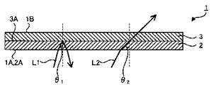
以下、本開示の拡散部材の第1実施態様について図面を参照して説明する。図1は、本開示の拡散部材の第1実施態様の一例を示す概略断面図である。図1に例示するように、拡散部材1は、第1層2と第2層3とをこの順で有する。第1層2は、光透過性および光拡散性を有しており、第1層2の第2層3側の面とは反対の面2Aから入射した光L1、L2を透過および拡散する。また、第2層3は、第2層3の第1層2側の面3Aに対する光の入射角の絶対値が小さくなるにつれて反射率が大きくなり、第2層3の第1層2側の面3Aに対する光の入射角の絶対値が大きくなるにつれて透過率が大きくなる。そのため、第2層3では、第2層3の第1層2側の面3Aに対して低入射角θ1で入射した光L1を反射させ、第2層3の第1層2側の面3Aに対して高入射角θ2で入射した光L2を透過させることができる。なお、低入射角とは、入射角の絶対値が小さいものをいい、高入射角とは、入射角の絶対値が大きいものをいう。
Hereinafter, the first embodiment of the diffusion member of the present disclosure will be described with reference to the drawings. FIG. 1 is a schematic cross-sectional view showing an example of the first embodiment of the diffusion member of the present disclosure. As illustrated in FIG. 1, the
図2は、本開示の第1実施態様の拡散部材を備える直下型方式のLEDバックライトの一例を示す概略断面図であり、図1に示す拡散部材を備える例である。図2に例示するように、LEDバックライト10は、支持基板12の一方の面にLED素子13が配置されたLED基板11と、LED基板11のLED素子13側の面側に配置された拡散部材1とを有する。拡散部材1は、第1層2側の面1AがLED基板11に対向するように配置される。なお、図2において、LED基板11と拡散部材1とは離れて配置されている。
FIG. 2 is a schematic cross-sectional view showing an example of a direct-type LED backlight provided with the diffusion member of the first embodiment of the present disclosure, and is an example including the diffusion member shown in FIG. As illustrated in FIG. 2, the
本開示においては、図1に示すように、拡散部材1の第1層2側の面1Aから入射した光を、第1層2で拡散させるとともに、第1層2を透過して拡散した光のうち、第2層3の第1層2側の面3Aに対して低入射角θ1で入射した光L1については、図2に示すように、第2層3の第1層2側の面3Aで反射させ、再び第1層2に入射させて拡散させることができる。そして、第1層2を透過して拡散した光のうち、第2層3の第1層2側の面3Aに対して高入射角θ2で入射した光L2、L2′については、第2層3を透過させ、拡散部材1の第2層3側の面1Bから出射させることができる。また、第1層および第2層を組み合わせることにより、拡散部材の第1層側の面から入射した光、特に拡散部材の第1層側の面から低入射角で入射した光について、何度も第1層を透過させて拡散させることができるので、拡散部材の第2層側の面から高出射角で出射させることができる。したがって、本開示の拡散部材を直下型方式のLEDバックライトに用いた場合には、LED素子から発せられる光を発光面全体に拡散させることができ、輝度の面内均一性を向上させることができる。
In the present disclosure, as shown in FIG. 1, the light incident from the
また、本開示においては、上述したように、第1層および第2層を組み合わせることにより、拡散部材の第1層側の面から低入射角で入射した光について、何度も第1層を透過させることができるため、光が拡散部材の第1層側の面から入射してから拡散部材の第2層側の面から出射するまでの光路長を長くすることができる。これにより、LED素子から発せられたのち拡散部材の第2層側の面から出射する光の一部を、LED素子の直上ではなく、LED素子から面内方向に離れた位置から出射させることができるようになる。したがって、本開示の拡散部材を備える直下型方式のLEDバックライトにおいては、LED素子と拡散部材との距離を短くした場合でも、輝度ムラを抑制することができる。よって、輝度の面内均一性を向上させつつ、薄型化を図ることが可能である。また、LED素子の数を減らした場合でも、輝度ムラを抑制することができる。そのため、輝度の均一化、薄型化、低コスト化、および低消費電力化を同時に実現することが可能である。 Further, in the present disclosure, as described above, by combining the first layer and the second layer, the first layer is repeatedly applied to the light incident from the surface of the diffusion member on the first layer side at a low incident angle. Since the light can be transmitted, the optical path length from when the light is incident from the surface on the first layer side of the diffusion member to when it is emitted from the surface on the second layer side of the diffusion member can be lengthened. As a result, a part of the light emitted from the surface of the diffusion member on the second layer side after being emitted from the LED element can be emitted from a position away from the LED element in the in-plane direction, not directly above the LED element. become able to. Therefore, in the direct type LED backlight provided with the diffusing member of the present disclosure, uneven brightness can be suppressed even when the distance between the LED element and the diffusing member is shortened. Therefore, it is possible to reduce the thickness while improving the in-plane uniformity of the brightness. Further, even when the number of LED elements is reduced, uneven brightness can be suppressed. Therefore, it is possible to simultaneously realize uniform brightness, thinning, cost reduction, and power consumption reduction.
また、本開示の拡散部材は、従来の透過反射板とは異なり、LED素子との位置合わせを不要とすることができる。そのため、本開示の拡散部材を用いることにより、LEDバックライトを容易に製造することができる。 Further, unlike the conventional transmission reflector, the diffusion member of the present disclosure can eliminate the need for alignment with the LED element. Therefore, the LED backlight can be easily manufactured by using the diffusion member of the present disclosure.
以下、本開示の拡散部材の第1実施態様について詳細に説明する。 Hereinafter, the first embodiment of the diffusion member of the present disclosure will be described in detail.
1.第1層
本開示における第1層は、後述の第2層の一方の面側に配置され、光透過性および光拡散性を有する部材である。
1. 1. First Layer The first layer in the present disclosure is a member that is arranged on one surface side of the second layer, which will be described later, and has light transmission and light diffusivity.
第1層が有する光透過性としては、例えば、第1層の全光線透過率が50%以上であることが好ましく、中でも70%以上であることが好ましく、特に90%以上であることが好ましい。第1層の全光線透過率が上記範囲であることにより、本開示の拡散部材をLEDバックライトに用いた場合に、輝度を高くすることができる。 As the light transmittance of the first layer, for example, the total light transmittance of the first layer is preferably 50% or more, particularly preferably 70% or more, and particularly preferably 90% or more. .. When the total light transmittance of the first layer is in the above range, the brightness can be increased when the diffusing member of the present disclosure is used for the LED backlight.
なお、第1層の全光線透過率は、例えば、JIS K7361−1:1997に準拠する方法により測定することができる。光源としては、CIE標準光源D65を用いることができる。 The total light transmittance of the first layer can be measured by, for example, a method based on JIS K7361-1: 1997. As the light source, the CIE standard light source D65 can be used.
第1層の光拡散性としては、例えば、光をランダムに拡散する光拡散性であってもよく、光を主に特定の方向に拡散する光拡散性であってもよい。光を主に特定の方向に拡散する光拡散性は、光を偏向する性質であり、すなわち光の進行方向を変化させる性質である。中でも、第1層の光拡散性は、光を主に特定の方向に拡散する光拡散性であることが好ましい。光を所定の方向に偏向する、すなわち光の進行方向を制御することにより、任意の形状や任意の強度分布に光を整形することができ、輝度の面内均一性をさらに向上させることができる。 The light diffusing property of the first layer may be, for example, a light diffusing property that randomly diffuses light, or a light diffusing property that mainly diffuses light in a specific direction. The light diffusivity that diffuses light mainly in a specific direction is a property that deflects light, that is, a property that changes the traveling direction of light. Above all, the light diffusivity of the first layer is preferably the light diffusivity that mainly diffuses light in a specific direction. By deflecting the light in a predetermined direction, that is, by controlling the traveling direction of the light, the light can be shaped into an arbitrary shape and an arbitrary intensity distribution, and the in-plane uniformity of brightness can be further improved. ..
第1層の光拡散性としては、光をランダムに拡散する光拡散性である場合、例えば、第1層に入射した光の拡散角が、10°以上とすることができ、15°以上であってもよく、20°以上であってもよい。また、第1層に入射した光の拡散角は、例えば、85°以下とすることができ、60°以下であってもよく、50°以下であってもよい。上記拡散角が上記範囲内であることにより、本開示の拡散部材をLEDバックライトに用いた場合に、輝度の面内均一性を向上させることができる。 As the light diffusivity of the first layer, when it is a light diffusing property that randomly diffuses light, for example, the diffusion angle of the light incident on the first layer can be 10 ° or more, and is 15 ° or more. It may be present, and it may be 20 ° or more. Further, the diffusion angle of the light incident on the first layer can be, for example, 85 ° or less, 60 ° or less, or 50 ° or less. When the diffusion angle is within the above range, the in-plane uniformity of brightness can be improved when the diffusion member of the present disclosure is used for an LED backlight.
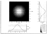
ここで、拡散角について説明する。図3は、透過光強度分布を例示するグラフであり、拡散角を説明する図である。本明細書においては、拡散部材を構成する第1層の一方の面に光を垂直に入射させて、第1層の他方の面から出射される光の最大透過光強度Imaxの2分の1になる2つの角度の差である半値幅(FWHM)を拡散角αと定義する。 Here, the diffusion angle will be described. FIG. 3 is a graph illustrating the transmitted light intensity distribution and is a diagram for explaining the diffusion angle. In the present specification, light is vertically incident on one surface of the first layer constituting the diffusion member, and is half of the maximum transmitted light intensity I max of the light emitted from the other surface of the first layer. The full width at half maximum (FWHM), which is the difference between two angles that become 1, is defined as the diffusion angle α.
なお、拡散角は、変角光度計や変角分光測色器を用いて測定することができる。拡散角の測定には、例えば、村上色彩技術研究所社製の変角光度計(ゴニオフォトメーター)GP−200等を用いることができる。 The diffusion angle can be measured using a variable angle photometer or a variable angle spectrophotometer. For the measurement of the diffusion angle, for example, a variable angle photometer (goniophotometer) GP-200 manufactured by Murakami Color Technology Research Institute can be used.
また、第1層の光拡散性としては、光を主に特定の方向に拡散する光拡散性である場合、第1層を透過した光の形状や強度分布等としては特に限定されるものではなく、光源の配光特性や、目的とする光の形状や強度分布等に応じて適宜選択される。第1層の光拡散性としては、例えば、非ガウシアン状の強度分布を有する光を出射する性質を挙げることができ、具体的には、環状の強度分布を有する光を出射する性質や、トップハット状の強度分布を有する光を出射する性質が挙げられる。図4(a)、(b)は環状の強度分布の例であり、図5はトップハット状の強度分布の例である。 Further, the light diffusivity of the first layer is not particularly limited as the shape, intensity distribution, etc. of the light transmitted through the first layer when the light diffusivity is such that the light is mainly diffused in a specific direction. However, it is appropriately selected according to the light distribution characteristics of the light source, the shape and intensity distribution of the target light, and the like. Examples of the light diffusivity of the first layer include the property of emitting light having a non-Gaussian-like intensity distribution, and specifically, the property of emitting light having an annular intensity distribution and the top. The property of emitting light having a hat-like intensity distribution can be mentioned. 4 (a) and 4 (b) are examples of an annular intensity distribution, and FIG. 5 is an example of a top hat-shaped intensity distribution.
中でも、第1層の光拡散性は、環状の強度分布を有する光を出射する性質であることが好ましい。特に、第1層の光拡散性は、環状の強度分布を有する光を出射する性質であって、例えば図4(a)に示すように、光軸中心に出射される透過光の強度がほぼゼロであることが好ましい。拡散部材の第1層側の面から入射した光を、第1層で環状に広げるとともに、第2層の第1層側の面に対して低入射角で入射した光については、第2層の第1層側の面で反射させ、再び第1層に入射させて環状に広げることができる。これを繰り返すことにより、拡散部材の第1層側の面から入射した光を横方向に広げることができる。したがって、本開示の拡散部材を直下型方式のLEDバックライトに用いた場合には、LED素子から発せられる光を発光面全体に拡散させることができ、輝度の面内均一性をより向上させることができるとともに、LED素子との位置合わせを不要とすることができる。 Above all, the light diffusivity of the first layer is preferably a property of emitting light having an annular intensity distribution. In particular, the light diffusivity of the first layer is a property of emitting light having an annular intensity distribution, and as shown in FIG. 4A, for example, the intensity of transmitted light emitted to the center of the optical axis is substantially the same. It is preferably zero. The light incident from the surface on the first layer side of the diffusing member is spread in a ring shape on the first layer, and the light incident on the surface on the first layer side of the second layer at a low incident angle is the second layer. It can be reflected on the surface on the first layer side of the light, then incident on the first layer again, and spread in an annular shape. By repeating this, the light incident from the surface of the diffusion member on the first layer side can be spread in the lateral direction. Therefore, when the diffusing member of the present disclosure is used for a direct type LED backlight, the light emitted from the LED element can be diffused over the entire light emitting surface, and the in-plane uniformity of brightness can be further improved. At the same time, it is possible to eliminate the need for alignment with the LED element.
ここで、上記強度分布は、変角光度計や変角分光測色器を用いて測定することができる。 Here, the intensity distribution can be measured using a variable angle photometer or a variable angle spectrophotometer.
第1層としては、上述の光透過性および光拡散性を有するものであれば特に限定されるものではなく、上述の光透過性および光拡散性を有する種々の構成を採用することができる。第1層としては、例えば、透過型回折格子、マイクロレンズアレイ、拡散剤および樹脂を含有する拡散剤含有樹脂膜等が挙げられる。具体的には、第1層が、光を主に特定の方向に拡散する光拡散性を有する場合、透過型回折格子、マイクロレンズアレイを挙げることができる。一方、第1層が、光をランダムに拡散する光拡散性を有する場合、拡散剤含有樹脂膜を挙げることができる。中でも、光拡散性の観点から、透過型回折格子、マイクロレンズアレイが好ましい。なお、透過型回折格子は、透過型の回折光学素子(DOE;Diffractive Optical Elements)とも称される。 The first layer is not particularly limited as long as it has the above-mentioned light transmission and light diffusivity, and various configurations having the above-mentioned light transmission and light diffusivity can be adopted. Examples of the first layer include a transmission type diffraction grating, a microlens array, a diffusing agent-containing resin film containing a diffusing agent and a resin, and the like. Specifically, when the first layer has a light diffusing property that mainly diffuses light in a specific direction, a transmission type diffraction grating and a microlens array can be mentioned. On the other hand, when the first layer has a light diffusive property of randomly diffusing light, a diffusing agent-containing resin film can be mentioned. Among them, a transmission type diffraction grating and a microlens array are preferable from the viewpoint of light diffusivity. The transmission type diffraction grating is also referred to as a transmission type diffraction optical element (DOE; Differential Optical Elements).
第1層が透過型回折格子である場合、透過型回折格子としては、上述の光透過性および光拡散性を有するものであれば特に限定されない。 When the first layer is a transmission type diffraction grating, the transmission type diffraction grating is not particularly limited as long as it has the above-mentioned light transmission and light diffusivity.
透過型回折格子としては、例えば、位相型回折格子および振幅型回折格子のいずれであってもよい。また、位相型回折格子は、例えば、レリーフ型回折格子および体積型回折格子のいずれであってもよい。中でも、透過型回折格子は、レリーフ型回折格子であることが好ましい。さらに、透過型回折格子がレリーフ型回折格子である場合、中でも、溝の断面形状が階段形状を有するマルチレベル回折格子であることが好ましい。一般にマルチレベル回折格子は回折格子のピッチが小さいことから、拡散部材とLED素子との位置合わせを不要とすることができる本開示は特に有効である。マルチレベル回折格子において、レベル数は、例えば2段、4段、8段、16段等とすることができる。図6はレベル数が4段であるマルチレベル回折格子2aの例である。 The transmission type diffraction grating may be, for example, either a phase type diffraction grating or an amplitude type diffraction grating. Further, the phase type diffraction grating may be, for example, either a relief type diffraction grating or a volumetric diffraction grating. Above all, the transmission type diffraction grating is preferably a relief type diffraction grating. Further, when the transmission type diffraction grating is a relief type diffraction grating, it is preferable that the groove is a multi-level diffraction grating having a stepped cross-sectional shape. In general, since the pitch of the diffraction grating is small in the multi-level diffraction grating, the present disclosure that can eliminate the need for alignment between the diffusion member and the LED element is particularly effective. In the multi-level diffraction grating, the number of levels can be, for example, 2 steps, 4 steps, 8 steps, 16 steps, or the like. FIG. 6 is an example of a multi-level diffraction grating 2a having four levels.
また、透過型回折格子としては、例えば、光を透過回折し、非ガウシアン状の強度分布を有する光を出射する透過型回折格子を挙げることができ、具体的には、光を透過回折し、環状の強度分布を有する光を出射する透過型回折格子や、光を透過回折し、トップハット状の強度分布を有する光を出射する透過型回折格子を挙げることができる。中でも、透過型回折格子は、光を透過回折し、環状の強度分布を有する光を出射する透過型回折格子である、すなわち、光を透過回折し、光軸中心に出射される透過回折光の強度と比較して、周辺部に出射される透過回折光の強度の方が強い環状の強度分布で透過回折光を出射する透過型回折格子であることが好ましい。特に、環状の強度分布で透過回折光を出射し、例えば図4(a)に示すように、光軸中心に出射される透過回折光の強度がほぼゼロである透過型回折格子であることが好ましい。このような透過型回折格子の場合、本開示の拡散部材をLEDバックライトに用いた場合に、光軸中心に出射される光の強度を小さくするとともに、周辺部に出射される光の強度を大きくすることができ、輝度の面内均一性をより向上させることができる。 Further, as the transmission type diffraction grating, for example, a transmission type diffraction grating that transmits and diffracts light and emits light having a non-Gaussian-like intensity distribution can be mentioned. Examples thereof include a transmission type diffraction grating that emits light having an annular intensity distribution and a transmission type diffraction grating that transmits and diffracts light and emits light having a top hat-like intensity distribution. Among them, the transmission type diffraction grating is a transmission type diffraction grating that transmits and diffracts light and emits light having an annular intensity distribution, that is, a transmission diffraction grating that transmits and diffracts light and emits transmitted diffracted light to the center of the optical axis. It is preferable that the transmission type diffraction grating emits the transmitted diffraction light with an annular intensity distribution in which the intensity of the transmitted diffracted light emitted to the peripheral portion is stronger than the intensity. In particular, it is a transmission type diffraction grating that emits transmitted diffracted light with an annular intensity distribution and, for example, as shown in FIG. 4A, the intensity of the transmitted diffracted light emitted to the center of the optical axis is almost zero. preferable. In the case of such a transmission type diffraction grating, when the diffusion member of the present disclosure is used for the LED backlight, the intensity of the light emitted to the center of the optical axis is reduced and the intensity of the light emitted to the peripheral portion is reduced. It can be increased and the in-plane uniformity of brightness can be further improved.
光を透過回折し、環状の強度分布を有する光を出射する透過型回折格子の場合、環状の強度分布において、透過回折光の強度が最大となる方向と、透過型回折格子の法線方向とのなす角度は、例えば、30°以上、75°以下とすることができる。上記角度が小さすぎると、光を横方向に広げる効果が十分に得られず、輝度の均一化が困難になるおそれがある。また、上記角度が大きすぎると、全反射が起こり、輝度の均一化が困難になるおそれがある。また、上記角度は、例えば、30°以上、45°以下であってもよい。上記角度が上記範囲内である場合には、透過型回折格子の作製が容易である。 In the case of a transmission type diffraction grating that transmits and diffracts light and emits light having an annular intensity distribution, in the annular intensity distribution, the direction in which the intensity of the transmitted diffraction light is maximized and the normal direction of the transmission type diffraction grating The angle formed by the grating can be, for example, 30 ° or more and 75 ° or less. If the angle is too small, the effect of spreading the light in the lateral direction cannot be sufficiently obtained, and it may be difficult to make the brightness uniform. Further, if the angle is too large, total reflection may occur and it may be difficult to make the brightness uniform. Further, the angle may be, for example, 30 ° or more and 45 ° or less. When the angle is within the above range, the transmission type diffraction grating can be easily manufactured.
ここで、上記強度分布および上記角度は、変角光度計や変角分光測色器を用いて測定することができる。上記角度の測定には、例えば、村上色彩技術研究所社製の変角光度計(ゴニオフォトメーター)GP−200、変角分光測色器GCMS−11等を用いることができる。 Here, the intensity distribution and the angle can be measured using a variable angle photometer or a variable angle spectrophotometer. For the measurement of the above angle, for example, a variable angle photometer (goniophotometer) GP-200 manufactured by Murakami Color Technology Research Institute, a variable angle spectrophotometer GCMS-11, or the like can be used.
透過型回折格子のピッチ等としては、上述の光透過性および光拡散性が得られればよく、適宜調整される。具体的には、LED素子の出力する波長が、赤色、緑色、青色等の単色である場合は、各波長に応じたピッチとすることで、効果的にLED素子からの光を曲げることが可能である。 The pitch and the like of the transmission type diffraction grating may be adjusted as appropriate as long as the above-mentioned light transmission and light diffusivity can be obtained. Specifically, when the wavelength output by the LED element is a single color such as red, green, or blue, it is possible to effectively bend the light from the LED element by setting the pitch according to each wavelength. Is.
具体的には、透過型回折格子のピッチは、50μm以上、200μm以下とすることができる。上述したように、本開示の拡散部材はLED素子との位置合わせを不要とすることができるため、透過型回折格子のピッチが上記範囲のように小さい場合には特に有効である。 Specifically, the pitch of the transmission type diffraction grating can be 50 μm or more and 200 μm or less. As described above, since the diffusion member of the present disclosure can eliminate the need for alignment with the LED element, it is particularly effective when the pitch of the transmission type diffraction grating is as small as the above range.
また、透過型回折格子がレリーフ型回折格子である場合、透過型回折格子の溝の深さは、例えば、1μm以上、5μm以下とすることができる。 When the transmission type diffraction grating is a relief type diffraction grating, the groove depth of the transmission type diffraction grating can be, for example, 1 μm or more and 5 μm or less.
なお、透過型回折格子のピッチとは、例えばマルチレベル回折格子の場合、図6に示すような、隣り合う溝の距離Pをいう。また、透過型回折格子の溝の深さとは、例えばマルチレベル回折格子の場合、図6に示すような、溝の最大深さd1をいう。 The pitch of the transmission type diffraction grating means, for example, in the case of a multi-level diffraction grating, the distance P of adjacent grooves as shown in FIG. Further, the groove depth of the transmission type diffraction grating means, for example, in the case of a multi-level diffraction grating, the maximum groove depth d1 as shown in FIG.
ここで、透過型回折格子のピッチおよび溝の深さは、透過型電子顕微鏡(TEM)、走査型電子顕微鏡(SEM)又は走査透過型電子顕微鏡(STEM)により観察される透過型回折格子の平面視顕微鏡写真又は透過型回折格子の厚さ方向の断面顕微鏡写真から求めることができる。 Here, the pitch and groove depth of the transmission type diffraction lattice are the planes of the transmission type diffraction lattice observed by a transmission electron microscope (TEM), a scanning electron microscope (SEM), or a scanning transmission electron microscope (STEM). It can be obtained from a scanning micrograph or a cross-sectional micrograph of a transmission electron diffraction lattice in the thickness direction.
透過型回折格子を構成する材料としては、上述の光透過性および光拡散性を有する透過型回折格子が得られる材料であればよく、一般的に透過型回折格子に用いられるものを採用することができる。例えば、石英ガラス等のガラスや、樹脂等が挙げられる。 The material constituting the transmissive diffraction grating may be any material that can obtain the above-mentioned transmissive diffraction grating having light transmissivity and light diffusivity, and a material generally used for the transmissive diffraction grating should be adopted. Can be done. For example, glass such as quartz glass, resin and the like can be mentioned.
また、透過型回折格子の形成方法としては、一般的な透過型回折格子の形成方法と同様とすることができる。透過型回折格子がマルチレベル回折格子である場合、透過型回折格子の形成方法としては、例えば、電子線やレーザの直接描画方式を用いたリソグラフィまたはフォトマスクを用いたリソグラフィにより石英基板等のガラス基板を加工する方法を挙げることができ、リソグラフィ工程およびエッチング工程を繰り返し行うことによって、ガラス基板に階段形状を有する溝を形成することができる。また、他の透過型回折格子の形成方法としては、金型による樹脂賦形を挙げることができる。この場合、例えば、基材層の一方の面に樹脂層を形成し、樹脂層を金型により賦形することにより、樹脂層に階段形状を有する溝を形成してもよく、第2層の一方の面に樹脂層を形成し、樹脂層を金型により賦形することにより、樹脂層に階段形状を有する溝を形成してもよい。金型の製造方法としては、まず、上記の電子線やレーザの直接描画方式を用いたリソグラフィまたはフォトマスクを用いたリソグラフィにより石英基板等のガラス基板を加工する方法により成形型を作製し、次に、この成形型を用いて反転型を作製する方法を挙げることができ、この反転型を金型として用いることができる。また、透過型回折格子の設計方法としては、例えば、反復フーリエ変換法(Iterative Fourier Transform Algorithm;IFTA)を用いることができる。 Further, the method for forming the transmission type diffraction grating can be the same as the method for forming the general transmission type diffraction grating. When the transmission type diffraction lattice is a multi-level diffraction lattice, as a method of forming the transmission type diffraction lattice, for example, a glass such as a quartz substrate is formed by etching using a direct drawing method of an electron beam or a laser or etching using a photomask. A method of processing a substrate can be mentioned, and a groove having a stepped shape can be formed on a glass substrate by repeating a lithography step and an etching step. Further, as another method for forming the transmission type diffraction grating, resin shaping by a mold can be mentioned. In this case, for example, a resin layer may be formed on one surface of the base material layer, and the resin layer may be shaped by a mold to form a groove having a stepped shape in the resin layer. A groove having a stepped shape may be formed in the resin layer by forming a resin layer on one surface and shaping the resin layer with a mold. As a method for manufacturing a mold, first, a mold is manufactured by a method of processing a glass substrate such as a quartz substrate by lithography using the above-mentioned direct drawing method of an electron beam or a laser or lithography using a photomask, and then the mold is manufactured. In addition, a method of producing an inversion mold using this molding mold can be mentioned, and this inversion mold can be used as a mold. Further, as a method for designing a transmission type diffraction grating, for example, an iterative Fourier transform algorithm (IFTA) can be used.
第1層がマイクロレンズアレイである場合、マイクロレンズアレイとしては、上述の光透過性および光拡散性を有するものであれば特に限定されない。 When the first layer is a microlens array, the microlens array is not particularly limited as long as it has the above-mentioned light transmission and light diffusivity.
また、マイクロレンズアレイとしては、例えば、光を透過屈折し、非ガウシアン状の強度分布を有する光を出射するマイクロレンズアレイを挙げることができ、具体的には、光を透過屈折し、環状の強度分布を有する光を出射するマイクロレンズアレイや、光を透過屈折し、トップハット状の強度分布を有する光を出射するマイクロレンズアレイを挙げることができる。中でも、マイクロレンズは、光を透過屈折し、環状の強度分布を有する光を出射するマイクロレンズアレイである、すなわち、光を透過屈折し、光軸中心に出射される透過屈折光の強度と比較して、周辺部に出射される透過屈折光の強度の方が強い環状の強度分布で透過屈折光を出射するマイクロレンズアレイであることが好ましい。このようなマイクロレンズアレイの場合、本開示の拡散部材をLEDバックライトに用いた場合に、光軸中心に出射される光の強度を小さくするとともに、周辺部に出射される光の強度を大きくすることができ、輝度の面内均一性をより向上させることができる。 Further, as the microlens array, for example, a microlens array that transmits and refracts light and emits light having a non-Gaussian-like intensity distribution can be mentioned. Examples thereof include a microlens array that emits light having an intensity distribution and a microlens array that transmits and refracts light and emits light having a top hat-like intensity distribution. Among them, the microlens is a microlens array that transmits and refracts light and emits light having an annular intensity distribution, that is, compared with the intensity of transmitted refracted light that transmits and refracts light and is emitted to the center of the optical axis. Therefore, it is preferable that the microlens array emits the transmitted refracted light with an annular intensity distribution in which the intensity of the transmitted refracted light emitted to the peripheral portion is stronger. In the case of such a microlens array, when the diffuser member of the present disclosure is used for the LED backlight, the intensity of the light emitted to the center of the optical axis is reduced and the intensity of the light emitted to the peripheral portion is increased. It is possible to further improve the in-plane uniformity of brightness.
マイクロレンズの形状、ピッチ、大きさ等としては、上述の光透過性および光拡散性が得られればよく、適宜調整される。 The shape, pitch, size, etc. of the microlens may be adjusted as appropriate as long as the above-mentioned light transmissivity and light diffusivity can be obtained.
具体的には、マイクロレンズアレイのマイクロレンズのピッチは、1mm以下とすることができ、0.6mm以下であってもよい。上述したように、本開示の拡散部材はLED素子との位置合わせを不要とすることができるため、マイクロレンズのピッチが上記範囲のように小さい場合には特に有効である。また、マイクロレンズのピッチは、例えば、0.001mm以上とすることができる。 Specifically, the pitch of the microlenses of the microlens array can be 1 mm or less, and may be 0.6 mm or less. As described above, since the diffusion member of the present disclosure can eliminate the need for alignment with the LED element, it is particularly effective when the pitch of the microlens is as small as the above range. Further, the pitch of the microlens can be, for example, 0.001 mm or more.
ここで、マイクロレンズのピッチは、透過型電子顕微鏡(TEM)、走査型電子顕微鏡(SEM)又は走査透過型電子顕微鏡(STEM)により観察されるマイクロレンズアレイの平面視顕微鏡写真又はマイクロレンズアレイの厚さ方向の断面顕微鏡写真から求めることができる。 Here, the pitch of the microlens is the planographic micrograph or microlens array of the microlens array observed by a transmission electron microscope (TEM), a scanning electron microscope (SEM) or a scanning transmission electron microscope (STEM). It can be obtained from a cross-sectional micrograph in the thickness direction.
マイクロレンズを構成する材料としては、上述の光透過性および光拡散性を有するマイクロレンズが得られる材料であればよく、一般的にマイクロレンズに用いられるものを採用することができる。また、マイクロレンズの形成方法としては、一般的なマイクロレンズの形成方法と同様とすることができる。 As the material constituting the microlens, any material that can obtain the above-mentioned microlens having light transmissivity and light diffusivity may be used, and materials generally used for microlenses can be adopted. Further, the method for forming the microlens can be the same as the method for forming the general microlens.
第1層が拡散剤含有樹脂膜である場合、拡散剤含有樹脂膜としては、上述の光透過性および光拡散性を有するものであれば特に限定されない。 When the first layer is a diffusing agent-containing resin film, the diffusing agent-containing resin film is not particularly limited as long as it has the above-mentioned light transmittance and light diffusivity.
拡散剤含有樹脂膜に含まれる拡散剤としては、LED素子からの光を拡散させることができれば特に限定されるものではなく、一般的にLEDバックライトに使用される拡散板に用いられる拡散剤を採用することができる。拡散剤含有樹脂膜中の拡散剤の含有量としては、LED素子からの光を拡散させることができれば特に限定されず、一般的にLEDバックライトに使用される拡散板における拡散剤の含有量と同様とすることができる。 The diffusing agent contained in the diffusing agent-containing resin film is not particularly limited as long as it can diffuse the light from the LED element, and a diffusing agent generally used for a diffusing plate used for an LED backlight is used. Can be adopted. The content of the diffusing agent in the diffusing agent-containing resin film is not particularly limited as long as the light from the LED element can be diffused, and is the content of the diffusing agent in the diffusing plate generally used for the LED backlight. The same can be done.
また、拡散剤含有樹脂膜に含まれる樹脂としては、拡散剤を分散させることができれば特に限定されるものではなく、一般的にLEDバックライトに使用される拡散板に用いられる樹脂を採用することができる。 Further, the resin contained in the diffusing agent-containing resin film is not particularly limited as long as the diffusing agent can be dispersed, and a resin generally used for a diffusing plate used for an LED backlight should be adopted. Can be done.
第1層は、光拡散性を発現することが可能な構造を有するものであればよく、例えば、層全体で光拡散性を発現するものであってもよく、面で光拡散性を発現するものであってもよい。面で光拡散性を発現するものとしては、例えば、レリーフ型回折格子やマイクロレンズアレイが挙げられる。一方、層全体で光拡散性を発現するものとしては、例えば、体積型回折格子や拡散剤含有樹脂膜が挙げられる。 The first layer may have a structure capable of exhibiting light diffusivity, for example, the first layer may exhibit light diffusivity in the entire layer, and exhibits light diffusivity on the surface. It may be a thing. Examples of those exhibiting light diffusivity on the surface include a relief type diffraction grating and a microlens array. On the other hand, examples of those that exhibit light diffusivity in the entire layer include a volumetric diffraction grating and a diffusing agent-containing resin film.
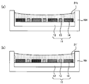
第1層および第2層の配置としては、例えば、第2層の一方の面に第1層が直接配置されていてもよく、第2層の一方の面に接着層または粘着層を介して第1層が配置されていてもよく、図7(a)に示すように第2層3の一方の面に空隙部を介して第1層2が配置されていてもよい。例えば、第1層が、面で光拡散性を発現するものである場合であって、第1層が、第2層と対向する面に光拡散性を発現することが可能な構造を有する場合には、第1層および第2層は空隙部を介して配置されることが好ましい。また、第2層の一方の面に第1層が直接配置されている場合には、例えば図7(b)に示すように、第2層3の一方の面にパターン状の第1層2が配置されていてもよい。例えば、第1層が、面で光拡散性を発現するものである場合には、第1層がパターン状に配置されている場合であっても、光拡散性を発現することができる。
As the arrangement of the first layer and the second layer, for example, the first layer may be directly arranged on one surface of the second layer, and the first layer may be arranged directly on one surface of the second layer via an adhesive layer or an adhesive layer. The first layer may be arranged, and as shown in FIG. 7A, the
第1層および第2層が空隙部を介して配置されている場合、第1層および第2層は接していてもよく、接していなくてもよい。第1層および第2層が接していない場合には、例えば第1層および第2層の間にはスペーサを配置することができる。また、空隙部は空気層とすることができる。 When the first layer and the second layer are arranged through the gap portion, the first layer and the second layer may or may not be in contact with each other. When the first layer and the second layer are not in contact with each other, for example, a spacer can be arranged between the first layer and the second layer. Further, the void portion can be an air layer.
第1層および第2層を積層する方法としては、例えば、第1層および第2層を接着層または粘着層を介して貼り合せる方法や、第2層の一方の面に第1層を直接形成する方法等が挙げられる。第2層の一方の面に第1層を直接形成する方法としては、例えば、印刷法、金型による樹脂賦形等が挙げられる。印刷法や金型による樹脂賦形の場合、第2層の一方の面にパターン状の第1層を直接形成することができる。 Examples of the method of laminating the first layer and the second layer include a method of bonding the first layer and the second layer via an adhesive layer or an adhesive layer, or a method of directly attaching the first layer to one surface of the second layer. Examples thereof include a method of forming. Examples of the method of directly forming the first layer on one surface of the second layer include a printing method and resin shaping by a mold. In the case of resin shaping by a printing method or a mold, a patterned first layer can be directly formed on one surface of the second layer.
2.第2層
本開示における第2層は、上記第1層の一方の面側に配置され、上記第2層の上記第1層側の面に対する光の入射角の絶対値が小さくなるにつれて反射率が大きくなるような反射率の入射角依存性と、上記第2層の上記第1層側の面に対する光の入射角の絶対値が大きくなるにつれて透過率が大きくなるような透過率の入射角依存性とを有する部材である。
2. Second layer The second layer in the present disclosure is arranged on one surface side of the first layer, and the reflectance decreases as the absolute value of the incident angle of light with respect to the surface of the second layer on the first layer side decreases. The incident angle of the reflectance increases so that the transmittance increases as the absolute value of the incident angle of light with respect to the surface of the second layer on the first layer side increases. It is a member having a dependency.
第2層は、第2層の第1層側の面に対する光の入射角の絶対値が小さくなるにつれて反射率が大きくなるような反射率の入射角依存性を有する。すなわち、第2層の第1層側の面に対して低入射角で入射する光の反射率は、第2層の第1層側の面に対して高入射角で入射する光の反射率よりも大きくなる。中でも、第2層の第1層側の面に対して低入射角で入射する光の反射率は、大きいことが好ましい。 The second layer has an incident angle dependence of the reflectance such that the reflectance increases as the absolute value of the incident angle of light with respect to the surface on the first layer side of the second layer decreases. That is, the reflectance of light incident on the surface of the second layer on the first layer side at a low incident angle is the reflectance of light incident on the surface of the second layer on the first layer side at a high incident angle. Will be larger than. Above all, it is preferable that the reflectance of light incident on the surface of the second layer on the first layer side at a low incident angle is large.
具体的には、第2層の第1層側の面に対して入射角±60°以内で入射する可視光の正反射率が、50%以上100%未満であることが好ましく、中でも80%以上100%未満であることが好ましく、特に90%以上100%未満であることが好ましい。なお、入射角±60°以内のすべての入射角において、可視光の正反射率が上記範囲を満たすことが好ましい。上記正反射率が上記範囲であることにより、本開示の拡散部材をLEDバックライトに用いた場合に、輝度の面内均一性を向上させることができる。 Specifically, the specular reflectance of visible light incident on the surface of the second layer on the first layer side within an incident angle of ± 60 ° is preferably 50% or more and less than 100%, particularly 80%. It is preferably 90% or more and less than 100%, and particularly preferably 90% or more and less than 100%. It is preferable that the specular reflectance of visible light satisfies the above range at all incident angles within ± 60 °. When the specular reflectance is in the above range, the in-plane uniformity of brightness can be improved when the diffusing member of the present disclosure is used for the LED backlight.
また、第2層の第1層側の面に対して入射角±60°以内で入射する可視光の正反射率の平均値は、例えば、80%以上99%以下であることが好ましく、中でも90%以上97%以下であることが好ましい。なお、上記正反射率の平均値とは、各入射角での可視光の正反射率の平均値をいう。上記正反射率の平均値が上記範囲であることにより、本開示の拡散部材をLEDバックライトに用いた場合に、輝度の面内均一性を向上させることができる。 Further, the average value of the specular reflectance of visible light incident on the surface of the second layer on the first layer side within an incident angle of ± 60 ° is preferably, for example, 80% or more and 99% or less. It is preferably 90% or more and 97% or less. The average value of the specular reflectance means the average value of the specular reflectance of visible light at each incident angle. When the average value of the specular reflectance is in the above range, the in-plane uniformity of brightness can be improved when the diffusing member of the present disclosure is used for the LED backlight.
また、第2層の第1層側の面に対して入射角0°で入射する(垂直に入射する)可視光の正反射率は、例えば、80%以上100%未満であることが好ましく、中でも90%以上100%未満であることが好ましく、特に95%以上100%未満であることが好ましい。上記正反射率が上記範囲であることにより、本開示の拡散部材をLEDバックライトに用いた場合に、輝度の面内均一性を向上させることができる。 Further, the specular reflectance of visible light that is incident (vertically incident) at an incident angle of 0 ° with respect to the surface of the second layer on the first layer side is preferably, for example, 80% or more and less than 100%. Above all, it is preferably 90% or more and less than 100%, and particularly preferably 95% or more and less than 100%. When the specular reflectance is in the above range, the in-plane uniformity of brightness can be improved when the diffusing member of the present disclosure is used for the LED backlight.
なお、「可視光」とは、本明細書では、波長380nm以上波長780nm以下の光を意味する。また、正反射率は、変角光度計や変角分光測色器を用いて測定することができる。正反射率の測定には、例えば、村上色彩技術研究所社製の変角光度計(ゴニオフォトメーター)GP−200、変角分光測色器GCMS−11等を用いることができる。 The term "visible light" as used herein means light having a wavelength of 380 nm or more and a wavelength of 780 nm or less. Further, the specular reflectance can be measured by using a variable angle photometer or a variable angle spectrophotometer. For the measurement of the specular reflectance, for example, a variable angle photometer (goniophotometer) GP-200 manufactured by Murakami Color Technology Research Institute, a variable angle spectrophotometer GCMS-11, or the like can be used.
また、第2層の第1層側の面に対して入射角±60°以内で入射する光の全光線透過率は、例えば、10%以下であることが好ましく、中でも5%以下であることが好ましく、特に3%以下であることが好ましい。なお、入射角±60°以内のすべての入射角において、全光線透過率が上記範囲を満たすことが好ましい。上記全光線透過率が上記範囲であれば、上記正反射率を所定の範囲内とすることができ、本開示の拡散部材をLEDバックライトに用いた場合に、輝度の面内均一性を向上させることができる。 Further, the total light transmittance of light incident on the surface of the second layer on the first layer side within an incident angle of ± 60 ° is preferably, for example, 10% or less, and above all, 5% or less. Is preferable, and particularly preferably 3% or less. It is preferable that the total light transmittance satisfies the above range at all the incident angles within ± 60 °. When the total light transmittance is within the above range, the specular reflectance can be within a predetermined range, and when the diffusing member of the present disclosure is used for the LED backlight, the in-plane uniformity of brightness is improved. Can be made to.
第2層は、第2層の第1層側の面に対する光の入射角の絶対値が大きくなるにつれて透過率が大きくなるような透過率の入射角依存性を有する。すなわち、第2層の第1層側の面に対して高入射角で入射する光の透過率は、第2層の第1層側の面に対して低入射角で入射する光の透過率よりも大きくなる。中でも、第2層の第1層側の面に対して高入射角で入射する光の透過率は、大きいことが好ましい。具体的には、第2層の第1層側の面に対して入射角70°以上90°未満で入射する光の全光線透過率が、30%以上であることが好ましく、中でも40%以上であることが好ましく、特に50%以上であることが好ましい。なお、入射角70°以上90°未満のすべての入射角において、全光線透過率が上記範囲を満たすことが好ましい。また、入射角の絶対値が70°以上90°未満の場合に、全光線透過率が上記範囲を満たすことが好ましい。上記全光線透過率が上記範囲であることにより、本開示の拡散部材をLEDバックライトに用いた場合に、輝度の面内均一性を向上させることができる。 The second layer has an incident angle dependence of the transmittance such that the transmittance increases as the absolute value of the incident angle of light with respect to the surface on the first layer side of the second layer increases. That is, the transmittance of light incident on the surface of the second layer on the first layer side at a high incident angle is the transmittance of light incident on the surface of the second layer on the first layer side at a low incident angle. Will be larger than. Above all, it is preferable that the transmittance of light incident on the surface of the second layer on the first layer side at a high incident angle is large. Specifically, the total light transmittance of light incident on the surface of the second layer on the first layer side at an incident angle of 70 ° or more and less than 90 ° is preferably 30% or more, particularly 40% or more. Is preferable, and particularly preferably 50% or more. It is preferable that the total light transmittance satisfies the above range at all incident angles of 70 ° or more and less than 90 °. Further, when the absolute value of the incident angle is 70 ° or more and less than 90 °, it is preferable that the total light transmittance satisfies the above range. When the diffuser member of the present disclosure is used for the LED backlight, the in-plane uniformity of brightness can be improved when the total light transmittance is in the above range.
なお、第2層の全光線透過率は、例えば、変角光度計や変角分光測色器を用いて、JIS K7361−1:1997に準拠する方法により測定することができる。全光線透過率の測定には、例えば、日本分光社製の紫外可視近赤外分光光度計 V−7200等を用いることができる。光源としては、CIE標準光源D65を用いることができる。 The total light transmittance of the second layer can be measured by a method according to JIS K7361-1: 1997, for example, using a variable angle photometer or a variable angle spectrophotometer. For the measurement of the total light transmittance, for example, an ultraviolet-visible near-infrared spectrophotometer V-7200 manufactured by JASCO Corporation can be used. As the light source, the CIE standard light source D65 can be used.
また、第2層の第1層側の面に対して入射角70°以上90°未満で入射する可視光の正反射率は、例えば、70%以下であることが好ましく、中でも60%以下であることが好ましく、特に50%以下であることが好ましい。なお、入射角70°以上90°未満のすべての入射角において、可視光の正反射率が上記範囲を満たすことが好ましい。また、入射角の絶対値が70°以上90°未満の場合に、可視光の正反射率が上記範囲を満たすことが好ましい。上記正反射率が上記範囲であれば、上記全光線透過率を所定の範囲内とすることができ、本開示の拡散部材をLEDバックライトに用いた場合に、輝度の面内均一性を向上させることができる。 Further, the specular reflectance of visible light incident on the surface of the second layer on the first layer side at an incident angle of 70 ° or more and less than 90 ° is preferably, for example, 70% or less, particularly 60% or less. It is preferably present, and particularly preferably 50% or less. It is preferable that the specular reflectance of visible light satisfies the above range at all incident angles of 70 ° or more and less than 90 °. Further, when the absolute value of the incident angle is 70 ° or more and less than 90 °, it is preferable that the specular reflectance of visible light satisfies the above range. When the specular reflectance is within the above range, the total light transmittance can be within a predetermined range, and when the diffusing member of the present disclosure is used for the LED backlight, the in-plane uniformity of brightness is improved. Can be made to.
また、第2層の第1層側の面に対して入射角70°以上90°未満で入射する可視光の正反射率の平均値は、例えば、70%以下であることが好ましく、中でも50%以下であることが好ましく、特に30%以下であることが好ましい。なお、上記正反射率の平均値とは、各入射角での可視光の正反射率の平均値をいう。上記正反射率の平均値が上記範囲であれば、上記全光線透過率を所定の範囲内とすることができ、本開示の拡散部材をLEDバックライトに用いた場合に、輝度の面内均一性を向上させることができる。 Further, the average value of the specular reflectance of visible light incident on the surface of the second layer on the first layer side at an incident angle of 70 ° or more and less than 90 ° is preferably, for example, 70% or less, particularly 50. % Or less, and particularly preferably 30% or less. The average value of the specular reflectance means the average value of the specular reflectance of visible light at each incident angle. When the average value of the specular reflectance is within the above range, the total light transmittance can be within a predetermined range, and when the diffuser member of the present disclosure is used for the LED backlight, the brightness is uniform in the plane. The sex can be improved.
第2層としては、上述した反射率および透過率の入射角依存性を有するものであれば特に限定されるものではなく、上述した反射率および透過率の入射角依存性を有する種々の構成を採用することができる。第2層としては、例えば、誘電体多層膜や、上記第1層側から順にパターン状の第1反射膜とパターン状の第2反射膜とを有し、第1反射膜の開口部および第2反射膜の開口部が平面視上重ならないように位置し、第1反射膜および第2反射膜が厚み方向に離れて配置されている反射構造体や、反射型回折格子等が挙げられる。 The second layer is not particularly limited as long as it has the above-mentioned reflectance and transmittance incident angle dependence, and various configurations having the above-mentioned reflectance and transmittance incident angle dependence are used. Can be adopted. The second layer includes, for example, a dielectric multilayer film, a patterned first reflective film and a patterned second reflective film in order from the first layer side, and has an opening of the first reflective film and a second layer. Examples thereof include a reflective structure in which the openings of the two reflective films are located so as not to overlap each other in a plan view, and the first reflective film and the second reflective film are arranged apart from each other in the thickness direction, a reflective diffraction grating, and the like.
以下、第2層が、誘電体多層膜、反射構造体、または反射型回折格子である場合について説明する。 Hereinafter, a case where the second layer is a dielectric multilayer film, a reflective structure, or a reflective diffraction grating will be described.
(1)誘電体多層膜
第2層が誘電体多層膜である場合、誘電体多層膜としては、例えば、屈折率の異なる無機層が交互に積層された無機化合物の多層膜や、屈折率の異なる樹脂層が交互に積層された樹脂の多層膜が挙げられる。
(1) Dielectric multilayer film When the second layer is a dielectric multilayer film, the dielectric multilayer film may be, for example, a multilayer film of an inorganic compound in which inorganic layers having different refractive indexes are alternately laminated, or a multilayer film having a refractive index. Examples thereof include a multilayer film of a resin in which different resin layers are alternately laminated.
(無機化合物の多層膜)
誘電体多層膜が、屈折率の異なる無機層が交互に積層された無機化合物の多層膜である場合、無機化合物の多層膜としては、上述した反射率および透過率の入射角依存性を有するものであれば特に限定されない。
(Multilayer film of inorganic compound)
When the dielectric multilayer film is a multilayer film of an inorganic compound in which inorganic layers having different refractive indexes are alternately laminated, the multilayer film of the inorganic compound has the above-mentioned reflectance and transmittance incident angle dependence. If so, it is not particularly limited.
屈折率が異なる無機層のうち、屈折率が高い高屈折率無機層に含まれる無機化合物としては、例えば、屈折率は1.7以上とすることができ、1.7以上2.5以下であってもよい。このような無機化合物としては、例えば、酸化チタン、酸化ジルコニウム、五酸化タンタル、五酸化ニオブ、酸化ランタン、酸化イットリウム、酸化亜鉛、硫化亜鉛、酸化インジウムを主成分とし、酸化チタン、酸化スズ、酸化セリウム等を少量含有させたもの等が挙げられる。 Among the inorganic layers having different refractive indexes, as the inorganic compound contained in the high refractive index inorganic layer having a high refractive index, for example, the refractive index can be 1.7 or more, and 1.7 or more and 2.5 or less. There may be. Examples of such inorganic compounds include titanium oxide, zirconium oxide, tantalum pentoxide, niobium pentoxide, lanthanum oxide, yttrium oxide, zinc oxide, zinc sulfide, and indium oxide as main components, and titanium oxide, tin oxide, and oxidation. Examples thereof include those containing a small amount of cerium and the like.
また、屈折率が異なる無機層のうち、屈折率が低い低屈折率無機層に含まれる無機化合物としては、例えば、屈折率は1.6以下とすることができ、1.2以上1.6以下であってもよい。このような無機化合物としては、例えば、シリカ、アルミナ、フッ化ランタン、フッ化マグネシウム、六フッ化アルミニウムナトリウム等が挙げられる。 Further, among the inorganic layers having different refractive indexes, as the inorganic compound contained in the low refractive index inorganic layer having a low refractive index, for example, the refractive index can be 1.6 or less, and 1.2 or more and 1.6. It may be as follows. Examples of such an inorganic compound include silica, alumina, lanthanum fluoride, magnesium fluoride, sodium hexafluoride, and the like.
高屈折率無機層および低屈折率無機層の積層数は、上述した反射率および透過率の入射角依存性が得られればよく、適宜調整される。具体的には、高屈折率無機層および低屈折率無機層の総積層数は、4層以上とすることができる。また、上記総積層数の上限としては特に限定されないが、積層数が多くなると工程が増えることから、例えば24層以下とすることができる。 The number of layers of the high-refractive index inorganic layer and the low-refractive index inorganic layer may be adjusted as appropriate as long as the above-mentioned reflectance and transmittance dependence on the incident angle can be obtained. Specifically, the total number of layers of the high-refractive-index inorganic layer and the low-refractive-index inorganic layer can be four or more. The upper limit of the total number of layers is not particularly limited, but the number of layers increases as the number of layers increases, so that the number of layers can be set to 24 or less, for example.
無機化合物の多層膜の厚みは、上述した反射率および透過率の入射角依存性が得られればよく、例えば、0.5μm以上10μm以下とすることができる。 The thickness of the multilayer film of the inorganic compound may be 0.5 μm or more and 10 μm or less, as long as the above-mentioned reflectance and transmittance depending on the incident angle can be obtained.
無機化合物の多層膜の形成方法としては、例えば、CVD法、スパッタリング法、真空蒸着法、または湿式塗工法等により、高屈折率無機層と低屈折率無機層とを交互に積層する方法が挙げられる。 Examples of the method for forming the multilayer film of the inorganic compound include a method of alternately laminating high refractive index inorganic layers and low refractive index inorganic layers by a CVD method, a sputtering method, a vacuum vapor deposition method, a wet coating method, or the like. Be done.
(樹脂の多層膜)
誘電体多層膜が、屈折率の異なる樹脂層が交互に積層された樹脂の多層膜である場合、樹脂の多層膜としては、上述した反射率および透過率の入射角依存性を有するものであれば特に限定されない。
(Multilayer film of resin)
When the dielectric multilayer film is a resin multilayer film in which resin layers having different refractive indexes are alternately laminated, the resin multilayer film may have the above-mentioned reflectance and transmittance incident angle dependence. There is no particular limitation.
樹脂層を構成する樹脂としては、例えば、熱可塑性樹脂、熱硬化性樹脂を挙げることができる。中でも、成形性が良好であることから、熱可塑性樹脂が好ましい。 Examples of the resin constituting the resin layer include a thermoplastic resin and a thermosetting resin. Among them, a thermoplastic resin is preferable because it has good moldability.
樹脂層には、各種添加剤、例えば、酸化防止剤、帯電防止剤、結晶核剤、無機粒子、有機粒子、減粘剤、熱安定剤、滑剤、赤外線吸収剤、紫外線吸収剤、屈折率調整のためのドープ剤等が添加されていてもよい。 Various additives such as antioxidants, antistatic agents, crystal nucleating agents, inorganic particles, organic particles, thickeners, heat stabilizers, lubricants, infrared absorbers, ultraviolet absorbers, and refractive index adjustments are added to the resin layer. A dope or the like may be added.
熱可塑性樹脂としては、例えば、ポリエチレン、ポリプロピレン、ポリスチレン、ポリメチルペンテン等のポリオレフィン樹脂、脂環族ポリオレフィン樹脂、ナイロン6、ナイロン66等のポリアミド樹脂、アラミド樹脂、ポリエチレンテレフタレート、ポリブチレンテレフタレート、ポリプロピレンテレフタレート、ポリブチルサクシネート、ポリエチレン−2,6−ナフタレート等のポリエステル樹脂、ポリカーボネート樹脂、ポリアリレート樹脂、ポリアセタール樹脂、ポリフェニレンサルファイド樹脂、4フッ化エチレン樹脂、3フッ化エチレン樹脂、3フッ化塩化エチレン樹脂、4フッ化エチレン−6フッ化プロピレン共重合体、フッ化ビニリデン樹脂等のフッ素樹脂、アクリル樹脂、メタクリル樹脂、ポリアセタール樹脂、ポリグリコール酸樹脂、ポリ乳酸樹脂等を用いることができる。中でも、強度、耐熱性、透明性の観点から、ポリエステルであることがより好ましい。
Examples of the thermoplastic resin include polyolefin resins such as polyethylene, polypropylene, polystyrene and polymethylpentene, alicyclic polyolefin resins, polyamide resins such as
本明細書において、ポリエステルとは、ジカルボン酸成分骨格とジオール成分骨格との重縮合体であるホモポリエステルや共重合ポリエステルのことをいう。ここで、ホモポリエステルとしては、例えば、ポリエチレンテレフタレート、ポリプロピレンテレフタレート、ポリブチレンテレフタレート、ポリエチレン−2,6−ナフタレート、ポリ−1,4−シクロヘキサンジメチレンテレフタレート、ポリエチレンジフェニルレート等が挙げられる。中でも、ポリエチレンテレフタレートは、安価であるため、非常に多岐にわたる用途に用いることができ好ましい。 In the present specification, the polyester refers to a homopolyester or a copolymerized polyester which is a polycondensate of a dicarboxylic acid component skeleton and a diol component skeleton. Here, examples of the homopolyester include polyethylene terephthalate, polypropylene terephthalate, polybutylene terephthalate, polyethylene-2,6-naphthalate, poly-1,4-cyclohexanedimethylene terephthalate, and polyethylene diphenyl rate. Among them, polyethylene terephthalate is preferable because it is inexpensive and can be used in a wide variety of applications.
また、本明細書において、共重合ポリエステルとは、次に挙げるジカルボン酸骨格を有する成分とジオール骨格を有する成分とより選ばれる少なくとも3つ以上の成分からなる重縮合体のことと定義される。ジカルボン酸骨格を有する成分としては、例えば、テレフタル酸、イソフタル酸、フタル酸、1,4−ナフタレンジカルボン酸、1,5−ナフタレンジカルボン酸、2,6−ナフタレンジカルボン酸、4,4−ジフェニルジカルボン酸、4,4−ジフェニルスルホンジカルボン酸、アジピン酸、セバシン酸、ダイマー酸、シクロヘキサンジカルボン酸とそれらのエステル誘導体等が挙げられる。グリコール骨格を有する成分としては、例えば、エチレングリコール、1,2−プロパンジオール、1,3−ブタンジオール、1,4−ブタンジオール、1,5−ペンタジオール、ジエチレングリコール、ポリアルキレングリコール、2,2−ビス(4−β−ヒドロキシエトキシフェニル)プロパン、イソソルベート、1,4−シクロヘキサンジメタノール、スピログリコール等が挙げられる。 Further, in the present specification, the copolymerized polyester is defined as a polycondensate composed of at least three or more components selected from the following components having a dicarboxylic acid skeleton and a component having a diol skeleton. Examples of the component having a dicarboxylic acid skeleton include terephthalic acid, isophthalic acid, phthalic acid, 1,4-naphthalenedicarboxylic acid, 1,5-naphthalenedicarboxylic acid, 2,6-naphthalenedicarboxylic acid, and 4,4-diphenyldicarboxylic acid. Examples thereof include acids, 4,4-diphenylsulfonedicarboxylic acids, adipic acids, sebacic acids, dimeric acids, cyclohexanedicarboxylic acids and their ester derivatives. Examples of the component having a glycol skeleton include ethylene glycol, 1,2-propanediol, 1,3-butanediol, 1,4-butanediol, 1,5-pentadiol, diethylene glycol, polyalkylene glycol, 2,2. Examples thereof include −bis (4-β-hydroxyethoxyphenyl) propane, isosorbate, 1,4-cyclohexanedimethanol, and spiroglycol.
屈折率が異なる樹脂層のうち、屈折率が高い高屈折率樹脂層と屈折率が低い低屈折率樹脂層との面内平均屈折率の差は、0.03以上であることが好ましく、より好ましくは0.05以上であり、さらに好ましくは0.1以上である。上記面内平均屈折率の差が小さすぎると、十分な反射率が得られない場合がある。 Among the resin layers having different refractive indexes, the difference in the in-plane average refractive index between the high refractive index resin layer having a high refractive index and the low refractive index resin layer having a low refractive index is preferably 0.03 or more. It is preferably 0.05 or more, and more preferably 0.1 or more. If the difference in the in-plane average refractive index is too small, sufficient reflectance may not be obtained.
また、高屈折率樹脂層の面内平均屈折率と厚み方向屈折率との差が、0.03以上であることが好ましく、低屈折率樹脂層の面内平均屈折率と厚み方向屈折率との差が、0.03以下であることが好ましい。この場合、入射角が大きくなっても、反射ピークの反射率の低下が起こりにくい。 Further, the difference between the in-plane average refractive index and the thickness direction refractive index of the high refractive index resin layer is preferably 0.03 or more, and the in-plane average refractive index and the thickness direction refractive index of the low refractive index resin layer The difference is preferably 0.03 or less. In this case, even if the incident angle is large, the reflectance of the reflection peak is unlikely to decrease.
高屈折率樹脂層に用いられる高屈折率樹脂と低屈折率樹脂層に用いられる低屈折率樹脂との好ましい組み合わせとしては、第一に、高屈折率樹脂および低屈折率樹脂のSP値の差の絶対値が、1.0以下であることが好ましい。SP値の差の絶対値が上記範囲であると、層間剥離が生じにくくなる。この場合、高屈折率樹脂および低屈折率樹脂が同一の基本骨格を含むことがより好ましい。ここで、基本骨格とは、樹脂を構成する繰り返し単位のことである。例えば、一方の樹脂がポリエチレンテレフタレートの場合、エチレンテレフタレートが基本骨格である。また例えば、一方の樹脂がポリエチレンの場合、エチレンが基本骨格である。高屈折率樹脂および低屈折率樹脂が同一の基本骨格を含む樹脂であると、さらに層間での剥離が生じにくくなる。 The preferred combination of the high refractive index resin used for the high refractive index resin layer and the low refractive index resin used for the low refractive index resin layer is, firstly, the difference in SP value between the high refractive index resin and the low refractive index resin. The absolute value of is preferably 1.0 or less. When the absolute value of the difference between the SP values is in the above range, delamination is less likely to occur. In this case, it is more preferable that the high refractive index resin and the low refractive index resin contain the same basic skeleton. Here, the basic skeleton is a repeating unit constituting the resin. For example, when one of the resins is polyethylene terephthalate, ethylene terephthalate is the basic skeleton. Further, for example, when one of the resins is polyethylene, ethylene is the basic skeleton. When the high-refractive index resin and the low-refractive index resin are resins containing the same basic skeleton, peeling between layers is more likely to occur.
高屈折率樹脂層に用いられる高屈折率樹脂と低屈折率樹脂層に用いられる低屈折率樹脂との好ましい組み合わせとしては、第二に、高屈折率樹脂および低屈折率樹脂のガラス転移温度の差が、20℃以下であることが好ましい。ガラス転移温度の差が大きすぎると、高屈折率樹脂層および低屈折率樹脂層の積層フィルムを製膜する際の厚み均一性が不良となる場合がある。また、上記積層フィルムを成形する際にも、過延伸が発生する場合がある。 The preferred combination of the high refractive index resin used for the high refractive index resin layer and the low refractive index resin used for the low refractive index resin layer is secondly, the glass transition temperature of the high refractive index resin and the low refractive index resin. The difference is preferably 20 ° C. or less. If the difference in the glass transition temperature is too large, the thickness uniformity when forming the laminated film of the high refractive index resin layer and the low refractive index resin layer may be poor. In addition, overstretching may occur when molding the laminated film.
また、高屈折率樹脂がポリエチレンテレフタレートまたはポリエチレンナフタレートであり、低屈折率樹脂がスピログリコールを含むポリエステルであることが好ましい。ここで、スピログリコールを含むポリエステルとは、スピログリコールを共重合したコポリエステル、またはホモポリエステル、またはそれらをブレンドしたポリエステルのことをいう。スピログリコールを含むポリエステルは、ポリエチレンテレフタレートやポリエチレンナフタレートとのガラス転移温度の差が小さいため、成形時に過延伸になりにくく、かつ層間剥離もしにくいために好ましい。より好ましくは、高屈折率樹脂がポリエチレンテレフタレートまたはポリエチレンナフタレートであり、低屈折率樹脂がスピログリコールおよびシクロヘキサンジカルボン酸を含むポリエステルであることが好ましい。低屈折率樹脂がスピログリコールおよびシクロヘキサンジカルボン酸を含むポリエステルであると、ポリエチレンテレフタレートやポリエチレンナフタレートとの面内屈折率の差が大きくなるため、高い反射率が得られやすくなる。また、ポリエチレンテレフタレートやポリエチレンナフタレートとのガラス転移温度の差が小さく、接着性にも優れるため、成形時に過延伸になりにくく、かつ層間剥離もしにくい。 Further, it is preferable that the high refractive index resin is polyethylene terephthalate or polyethylene naphthalate, and the low refractive index resin is polyester containing spiroglycol. Here, the polyester containing spiroglycol refers to a copolyester in which spiroglycol is copolymerized, a homopolyester, or a polyester in which they are blended. Polyester containing spiroglycol is preferable because the difference in glass transition temperature between polyethylene terephthalate and polyethylene naphthalate is small, so that overstretching is unlikely to occur during molding and delamination is also difficult to occur. More preferably, the high refractive index resin is polyethylene terephthalate or polyethylene naphthalate, and the low refractive index resin is a polyester containing spiroglycol and cyclohexanedicarboxylic acid. When the low refractive index resin is a polyester containing spiroglycol and cyclohexanedicarboxylic acid, the difference in in-plane refractive index from polyethylene terephthalate or polyethylene naphthalate becomes large, so that high reflectance can be easily obtained. Further, since the difference in glass transition temperature between polyethylene terephthalate and polyethylene naphthalate is small and the adhesiveness is excellent, overstretching is unlikely to occur during molding and delamination is also difficult to occur.
また、高屈折率樹脂がポリエチレンテレフタレートまたはポリエチレンナフタレートであり、低屈折率樹脂がシクロヘキサンジメタノールを含むポリエステルであることも好ましい。ここで、シクロヘキサンジメタノールを含むポリエステルとは、シクロヘキサンジメタノールを共重合したコポリエステル、またはホモポリエステル、またはそれらをブレンドしたポリエステルのことをいう。シクロヘキサンジメタノールを含むポリエステルは、ポリエチレンテレフタレートやポリエチレンナフタレートとのガラス転移温度の差が小さいため、成形時に過延伸になることがなりにくく、かつ層間剥離もしにくいために好ましい。この場合、低屈折率樹脂は、シクロヘキサンジメタノールの共重合量が15mol%以上60mol%以下であるエチレンテレフタレート重縮合体であることがより好ましい。このようにすることにより、高い反射性能を有しながら、特に加熱や経時による光学的特性の変化が小さく、層間での剥離も生じにくくなる。シクロヘキサンジメタノールの共重合量が上記範囲内であるエチレンテレフタレート重縮合体は、ポリエチレンテレフタレートと非常に強く接着する。また、そのシクロヘキサンジメタノール基は幾何異性体としてシス体あるいはトランス体があり、また配座異性体としてイス型あるいはボート型もあるので、ポリエチレンテレフタレートと共延伸しても配向結晶化しにくく、高反射率で、熱履歴による光学特性の変化もさらに少なく、製膜時のやぶれも生じにくい。 It is also preferable that the high refractive index resin is polyethylene terephthalate or polyethylene naphthalate, and the low refractive index resin is polyester containing cyclohexanedimethanol. Here, the polyester containing cyclohexanedimethanol refers to a copolyester obtained by copolymerizing cyclohexanedimethanol, a homopolyester, or a polyester blended thereto. Polyester containing cyclohexanedimethanol is preferable because the difference in glass transition temperature between polyethylene terephthalate and polyethylene naphthalate is small, so that overstretching is unlikely to occur during molding and delamination is also difficult to occur. In this case, the low refractive index resin is more preferably an ethylene terephthalate polycondensate having a copolymerization amount of cyclohexanedimethanol of 15 mol% or more and 60 mol% or less. By doing so, while having high reflection performance, the change in optical characteristics due to heating and aging is particularly small, and peeling between layers is less likely to occur. The ethylene terephthalate polycondensate having a copolymerization amount of cyclohexanedimethanol within the above range adheres very strongly to polyethylene terephthalate. In addition, the cyclohexanedimethanol group has a cis isomer or a trans isomer as a geometric isomer, and also has a chair type or a boat type as a conformation isomer. Therefore, even if co-stretched with polyethylene terephthalate, orientation crystallization is difficult and high reflectance is achieved. In terms of reflectance, the change in optical characteristics due to thermal history is even smaller, and blurring during film formation is less likely to occur.
上記の樹脂の多層膜においては、高屈折率樹脂層と低屈折率樹脂層とが厚み方向に交互に積層された構造を有している部分が存在していればよい。すなわち、高屈折率樹脂層および低屈折率樹脂層の厚み方向における配置の序列がランダムな状態ではないことが好ましく、高屈折率樹脂層および低屈折率樹脂層以外の樹脂層の配置の序列については特に限定されるものではない。また、上記の樹脂の多層膜が、高屈折率樹脂層と低屈折率樹脂層と他の樹脂層とを有する場合、それらの配置の順列としては、高屈折率樹脂層をA、低屈折率樹脂層をB、他の樹脂層をCとしたとき、A(BCA)n、A(BCBA)n、A(BABCBA)n等の規則的順列で各層が積層されることがより好ましい。ここで、nは繰り返しの単位数であり、例えばA(BCA)nにおいてn=3の場合、厚み方向にABCABCABCAの順列で積層されているものを表す。 In the multilayer film of the above resin, it is sufficient that there is a portion having a structure in which the high refractive index resin layer and the low refractive index resin layer are alternately laminated in the thickness direction. That is, it is preferable that the arrangement of the high refractive index resin layer and the low refractive index resin layer in the thickness direction is not in a random state, and the arrangement of the resin layers other than the high refractive index resin layer and the low refractive index resin layer is arranged. Is not particularly limited. When the multilayer film of the above resin has a high refractive index resin layer, a low refractive index resin layer, and another resin layer, the arrangement of the multilayer film is such that the high refractive index resin layer is A and the low refractive index is low. When the resin layer is B and the other resin layer is C, it is more preferable that the layers are laminated in a regular order such as A (BCA) n, A (BCBA) n, and A (BABCBA) n. Here, n is the number of repeating units. For example, when n = 3 in A (BCA) n, it represents those stacked in the order of ABCABCABCA in the thickness direction.
また、高屈折率樹脂層および低屈折率樹脂層の積層数は、上述した反射率および透過率の入射角依存性が得られればよく、適宜調整される。具体的には、高屈折率樹脂層と低屈折率樹脂層とは交互にそれぞれ30層以上積層することができ、それぞれ200層以上積層してもよい。また、高屈折率樹脂層および低屈折率樹脂層の総積層数は、例えば600層以上とすることができる。積層数が少なすぎると、十分な反射率が得られなくなる場合がある。また、積層数が上記範囲であることにより、所望の反射率を容易に得ることができる。また、上記総積層数の上限としては特に限定されないが、装置の大型化や層数が多くなりすぎることによる積層精度の低下を考慮すると、例えば1500層以下とすることができる。 Further, the number of layers of the high-refractive index resin layer and the low-refractive index resin layer may be adjusted as appropriate as long as the above-mentioned reflectance and transmittance depending on the incident angle can be obtained. Specifically, the high-refractive index resin layer and the low-refractive index resin layer can be alternately laminated with 30 or more layers, and 200 or more layers may be laminated with each other. The total number of layers of the high-refractive index resin layer and the low-refractive index resin layer can be, for example, 600 or more. If the number of layers is too small, sufficient reflectance may not be obtained. Further, when the number of layers is in the above range, a desired reflectance can be easily obtained. The upper limit of the total number of layers is not particularly limited, but may be 1500 layers or less in consideration of a decrease in stacking accuracy due to an increase in the size of the apparatus and an excessive number of layers.
さらに、上記の樹脂の多層膜は、少なくとも片面に厚み3μm以上のポリエチレンテレフタレートまたはポリエチレンナフタレートを含有する表面層を有することが好ましく、中でも両面に上記表面層を有することが好ましい。また、表面層の厚みは5μm以上であることがより好ましい。上記表面層を有することにより、上記の樹脂の多層膜の表面を保護することができる。 Further, the multilayer film of the resin preferably has a surface layer containing polyethylene terephthalate or polyethylene naphthalate having a thickness of 3 μm or more on at least one side, and more preferably has the surface layers on both sides. Further, the thickness of the surface layer is more preferably 5 μm or more. By having the surface layer, the surface of the multilayer film of the resin can be protected.
上記の樹脂の多層膜の製造方法としては、例えば、共押出法等が挙げられる。具体的には、特開2008−200861号公報に記載の積層フィルムの製造方法を参照することができる。 Examples of the method for producing the above-mentioned resin multilayer film include a coextrusion method and the like. Specifically, the method for producing a laminated film described in JP-A-2008-200861 can be referred to.
また、上記の樹脂の多層膜としては、市販の積層フィルムを用いることができ、具体的には、東レ株式会社製のピカサス(登録商標)、3M社製のESR等が挙げられる。 Further, as the multilayer film of the above resin, a commercially available laminated film can be used, and specific examples thereof include Picasas (registered trademark) manufactured by Toray Industries, Inc. and ESR manufactured by 3M.
(2)反射構造体
反射構造体は、上記第1層側から順にパターン状の第1反射膜とパターン状の第2反射膜とを有し、第1反射膜の開口部および第2反射膜の開口部が平面視上重ならないように位置し、第1反射膜および第2反射膜が厚み方向に離れて配置されているものである。
(2) Reflective structure The reflective structure has a patterned first reflective film and a patterned second reflective film in this order from the first layer side, and has an opening of the first reflective film and a second reflective film. The openings of the above are located so as not to overlap in a plan view, and the first reflective film and the second reflective film are arranged apart from each other in the thickness direction.
反射構造体は、2つの態様を有する。反射構造体の第1態様は、透明基材と、透明基材の一方の面に配置されたパターン状の第1反射膜と、透明基材の他方の面に配置されたパターン状の第2反射膜とを有し、第1反射膜の開口部および第2反射膜の開口部が平面視上重ならないように位置し、第1反射膜および第2反射膜が厚み方向に離れて配置されているものである。また、反射構造体の第2態様は、透明基材と、透明基材の一方の面に配置され、光透過性を有するパターン状の凸部と、凸部の透明基材側の面とは反対の面側に配置されたパターン状の第1反射膜と、透明基材の一方の面の凸部の開口部に配置されたパターン状の第2反射膜とを有し、第1反射膜の開口部および第2反射膜の開口部が平面視上重ならないように位置し、第1反射膜および第2反射膜が厚み方向に離れて配置されているものである。以下、各態様に分けて説明する。 The reflective structure has two aspects. The first aspect of the reflective structure is a transparent base material, a patterned first reflective film arranged on one surface of the transparent base material, and a patterned second surface arranged on the other surface of the transparent base material. It has a reflective film, the opening of the first reflective film and the opening of the second reflective film are located so as not to overlap in a plan view, and the first reflective film and the second reflective film are arranged apart from each other in the thickness direction. Is what you are doing. Further, in the second aspect of the reflective structure, the transparent base material, the patterned convex portion arranged on one surface of the transparent base material and having light transmittance, and the surface of the convex portion on the transparent base material side are It has a patterned first reflective film arranged on the opposite surface side and a patterned second reflective film arranged in the opening of the convex portion on one surface of the transparent base material, and is the first reflective film. The opening of the first reflective film and the opening of the second reflective film are located so as not to overlap each other in a plan view, and the first reflective film and the second reflective film are arranged apart from each other in the thickness direction. Hereinafter, each aspect will be described separately.
(反射構造体の第1態様)
本開示における反射構造体の第1態様は、透明基材と、透明基材の一方の面に配置されたパターン状の第1反射膜と、透明基材の他方の面に配置されたパターン状の第2反射膜とを有し、第1反射膜の開口部および第2反射膜の開口部が平面視上重ならないように位置し、第1反射膜および第2反射膜が厚み方向に離れて配置されているものである。本態様の反射構造体の場合、本開示の拡散部材において、反射構造体の第1反射膜側の面側に第1層が配置される。
(First aspect of reflective structure)
The first aspect of the reflective structure in the present disclosure is a transparent substrate, a patterned first reflective film arranged on one surface of the transparent substrate, and a patterned first reflective film arranged on the other surface of the transparent substrate. The first reflective film and the second reflective film are located so that the openings of the first reflective film and the second reflective film do not overlap in a plan view, and the first reflective film and the second reflective film are separated from each other in the thickness direction. Is arranged. In the case of the reflective structure of this embodiment, in the diffusion member of the present disclosure, the first layer is arranged on the surface side of the reflective structure on the first reflective film side.
図8(a)、(b)は、本態様の反射構造体の一例を示す概略平面図および断面図であり、図8(a)は反射構造体の第1反射膜側の面から見た平面図であり、図8(b)は図8(a)のA−A線断面図である。図8(a)、(b)に示すように、反射構造体20は、透明基材21と、透明基材21の一方の面に配置されたパターン状の第1反射膜22と、透明基材21の他方の面に配置された第2反射膜24とを有している。第1反射膜22の開口部23および第2反射膜24の開口部25は、平面視上重ならないように位置している。また、第1反射膜22および第2反射膜24は、透明基材21の両面にそれぞれ配置されており、厚み方向に離れて配置されている。なお、図8(a)において、第2反射膜の開口部は破線で示している。また、図8(c)は、本態様の反射構造体を有する拡散部材を備えるLEDバックライトの一例を示す概略断面図である。
8 (a) and 8 (b) are schematic plan views and cross-sectional views showing an example of the reflective structure of this embodiment, and FIG. 8 (a) is seen from the surface of the reflective structure on the first reflective film side. It is a plan view, and FIG. 8 (b) is a sectional view taken along line AA of FIG. 8 (a). As shown in FIGS. 8A and 8B, the
このような反射構造体においては、パターン状の第1反射膜および第2反射膜が積層されており、第1反射膜の開口部および第2反射膜の開口部が平面視上重ならないように位置していることから、本態様の反射構造体を有する拡散部材をLEDバックライトに用いた場合、例えば図8(c)に示すように、LED素子13の直上には第1反射膜22および第2反射膜24の少なくともいずれか一方が必ず存在することになる。そのため、例えば図8(b)に示すように、反射構造体20の第1反射膜22側の面、すなわち反射構造体20(第2層)の第1層(図示なし)が配置される側の面3Aに対して低入射角で入射した光L11を、第1反射膜22および第2反射膜24で反射させることができる。また、第1反射膜の開口部および第2反射膜の開口部が平面視上重ならないように位置し、第1反射膜および第2反射膜が厚み方向に離れて配置されていることから、反射構造体20の第1反射膜22側の面、すなわち反射構造体20(第2層)の第1層(図示なし)が配置される側の面3Aに対して高入射角で入射した光L12、L13を、第1反射膜22の開口部23および第2反射膜24の開口部25から出射させることができる。これにより、LED素子から発せられたのち拡散部材の第2層側の面から出射する光の一部を、LED素子の直上ではなく、LED素子から面内方向に離れた位置から出射させることができるようになる。よって、輝度の面内均一性を向上させることができる。
In such a reflective structure, the patterned first reflective film and the second reflective film are laminated so that the openings of the first reflective film and the openings of the second reflective film do not overlap in a plan view. Since it is located, when the diffusion member having the reflective structure of this embodiment is used for the LED backlight, for example, as shown in FIG. 8C, the first
以下、本態様の反射構造体について説明する。 Hereinafter, the reflective structure of this embodiment will be described.
第1反射膜および第2反射膜としては、一般的な反射膜を用いることができ、例えば、金属膜、誘電体多層膜等を用いることができる。金属膜の材料としては、一般的な反射膜に使用される金属材料を採用することができ、例えば、アルミニウム、金、銀、およびそれらの合金等が挙げられる。また、誘電体多層膜としては、一般的な反射膜に使用されるものを採用することができ、例えば、酸化ジルコニウムと酸化ケイ素とが交互に積層された多層膜等の無機化合物の多層膜が挙げられる。第1反射膜および第2反射膜に含まれる材料は、同一であってもよく、互いに異なっていてもよい。 As the first reflective film and the second reflective film, a general reflective film can be used, and for example, a metal film, a dielectric multilayer film, or the like can be used. As the material of the metal film, a metal material used for a general reflective film can be adopted, and examples thereof include aluminum, gold, silver, and alloys thereof. Further, as the dielectric multilayer film, those used for general reflective films can be adopted. For example, a multilayer film of an inorganic compound such as a multilayer film in which zirconium oxide and silicon oxide are alternately laminated can be used. Can be mentioned. The materials contained in the first reflective film and the second reflective film may be the same or different from each other.
第1反射膜および第2反射膜の開口部のピッチとしては、上述した反射率および透過率の入射角依存性が得られればよく、本開示の拡散部材が用いられるLEDバックライトにおけるLED素子の配光特性、サイズ、ピッチおよび形状や、LED基板と拡散部材との距離等に応じて適宜設定される。第1反射膜および第2反射膜の開口部のピッチは、同一であってもよく、互いに異なっていてもよい。 As the pitch of the openings of the first reflective film and the second reflective film, it is sufficient that the above-mentioned reflectance and transmittance depend on the incident angle, and the LED element in the LED backlight in which the diffusion member of the present disclosure is used. It is appropriately set according to the light distribution characteristics, size, pitch and shape, the distance between the LED substrate and the diffuser member, and the like. The pitches of the openings of the first reflective film and the second reflective film may be the same or different from each other.
第1反射膜の開口部のピッチは、例えば、LED素子のサイズよりも大きくてもよい。具体的には、第1反射膜の開口部のピッチは、0.1mm以上20mm以下とすることができる。 The pitch of the openings of the first reflective film may be larger than the size of the LED element, for example. Specifically, the pitch of the openings of the first reflective film can be 0.1 mm or more and 20 mm or less.
また、第2反射膜の開口部のピッチは、輝度ムラを抑制することができれば特に限定されないが、中でも、上記第1反射膜の開口部のピッチ以下であることが好ましく、上記第1反射膜の開口部のピッチより小さいことが好ましい。具体的には、第2反射膜の開口部のピッチは、0.1mm以上2mm以下とすることができる。上記のように第2反射膜の開口部のピッチを微細にすることにより、第2反射膜の部分と第2反射膜の開口部の部分とのパターンを視認しにくくすることができ、ムラのない面発光が可能となる。 The pitch of the opening of the second reflective film is not particularly limited as long as the uneven brightness can be suppressed, but it is preferably equal to or less than the pitch of the opening of the first reflective film, and the pitch of the opening of the first reflective film is particularly preferable. It is preferably smaller than the pitch of the opening of. Specifically, the pitch of the opening of the second reflective film can be 0.1 mm or more and 2 mm or less. By making the pitch of the opening of the second reflective film fine as described above, it is possible to make it difficult to visually recognize the pattern between the portion of the second reflective film and the portion of the opening of the second reflective film. No surface emission is possible.
なお、第1反射膜の開口部のピッチとは、例えば図8(a)に示すような、隣り合う第1反射膜22の開口部23の中心間の距離P1をいう。また、第2反射膜の開口部のピッチとは、例えば図8(a)に示すような、隣り合う第2反射膜24の開口部25の中心間の距離P2をいう。
The pitch of the openings of the first reflective film refers to the distance P1 between the centers of the
第1反射膜および第2反射膜の開口部の大きさとしては、上述した反射率および透過率の入射角依存性が得られればよく、本開示の拡散部材が用いられるLEDバックライトにおけるLED素子の配光特性、サイズ、ピッチおよび形状や、LED基板と拡散部材との距離等に応じて適宜設定される。第1反射膜および第2反射膜の開口部の大きさは、同一であってもよく、互いに異なっていてもよい。 As the size of the openings of the first reflective film and the second reflective film, it is sufficient that the above-mentioned reflectance and transmittance depend on the incident angle, and the LED element in the LED backlight in which the diffusion member of the present disclosure is used. It is appropriately set according to the light distribution characteristics, size, pitch and shape of the LED substrate, the distance between the LED substrate and the diffuser member, and the like. The sizes of the openings of the first reflective film and the second reflective film may be the same or different from each other.
第1反射膜の開口部の大きさとしては、具体的には、第1反射膜の開口部の形状が矩形状である場合、第1反射膜の開口部の長さは、0.1mm以上5mm以下とすることができる。 Regarding the size of the opening of the first reflective film, specifically, when the shape of the opening of the first reflective film is rectangular, the length of the opening of the first reflective film is 0.1 mm or more. It can be 5 mm or less.
また、第2反射膜の開口部の大きさは、輝度ムラを抑制することができれば特に限定されないが、中でも、上記第1反射膜の開口部の大きさ以下であることが好ましく、上記第1反射膜の開口部の大きさより小さいことが好ましい。具体的には、第2反射膜の開口部の形状が矩形状である場合、第2反射膜の開口部の長さは、0.05mm以上2mm以下とすることができる。上記のように第2反射膜の開口部の大きさを微細にすることにより、第2反射膜の部分と第2反射膜の開口部の部分とのパターンを視認しにくくすることができ、ムラのない面発光が可能となる。 The size of the opening of the second reflective film is not particularly limited as long as the uneven brightness can be suppressed, but the size of the opening of the first reflective film is preferably smaller than that of the first reflective film. It is preferably smaller than the size of the opening of the reflective film. Specifically, when the shape of the opening of the second reflective film is rectangular, the length of the opening of the second reflective film can be 0.05 mm or more and 2 mm or less. By making the size of the opening of the second reflective film fine as described above, it is possible to make it difficult to visually recognize the pattern between the portion of the second reflective film and the portion of the opening of the second reflective film, resulting in unevenness. It is possible to emit light from the surface without any light.
なお、第1反射膜の開口部の大きさとは、例えば第1反射膜の開口部の形状が矩形状である場合、図8(a)に示すような、第1反射膜22の開口部23の長さx1をいう。また、第2反射膜の開口部の大きさとは、例えば図8(a)に示すような、第2反射膜24の開口部25の長さx2をいう。
The size of the opening of the first reflective film is, for example, when the shape of the opening of the first reflective film is rectangular, the
第1反射膜および第2反射膜の開口部の形状としては、例えば、矩形状、円形状等、任意の形状とすることができる。 The shape of the openings of the first reflective film and the second reflective film can be any shape such as a rectangular shape and a circular shape.
第1反射膜および第2反射膜の厚みとしては、上述した反射率および透過率の入射角依存性が得られればよく、適宜調整される。具体的には、第1反射膜および第2反射膜の厚みは、0.05μm以上100μm以下とすることができる。 The thicknesses of the first reflective film and the second reflective film are appropriately adjusted as long as the above-mentioned reflectance and transmittance depending on the incident angle can be obtained. Specifically, the thickness of the first reflective film and the second reflective film can be 0.05 μm or more and 100 μm or less.
第1反射膜および第2反射膜は、透明基材の面に形成されたものであってもよく、シート状の反射膜であってもよい。第1反射膜および第2反射膜の形成方法としては、透明基材の面にパターン状に反射膜を形成できる方法であれば特に限定されず、例えば、スパッタリング法、真空蒸着法等が挙げられる。また、第1反射膜および第2反射膜がシート状の反射膜である場合、開口部の形成方法としては、例えば、打ち抜き加工等により複数の貫通孔を形成する方法等が挙げられる。この場合、透明基材およびシート状の反射膜の積層方法としては、例えば、透明基材に接着層や粘着層を介してシート状の反射膜を貼り合せる方法を用いることができる。 The first reflective film and the second reflective film may be formed on the surface of the transparent base material, or may be a sheet-shaped reflective film. The method for forming the first reflective film and the second reflective film is not particularly limited as long as it can form the reflective film in a pattern on the surface of the transparent substrate, and examples thereof include a sputtering method and a vacuum vapor deposition method. .. When the first reflective film and the second reflective film are sheet-shaped reflective films, examples of the method for forming the openings include a method of forming a plurality of through holes by punching or the like. In this case, as a method of laminating the transparent base material and the sheet-shaped reflective film, for example, a method of laminating the sheet-shaped reflective film to the transparent base material via an adhesive layer or an adhesive layer can be used.
本態様の反射構造体における透明基材は、上記の第1反射膜および第2反射膜等を支持する部材であり、また、第1反射膜および第2反射膜を厚み方向に離れて配置させるための部材である。 The transparent base material in the reflective structure of this embodiment is a member that supports the first reflective film, the second reflective film, and the like, and the first reflective film and the second reflective film are arranged apart from each other in the thickness direction. It is a member for.
透明基材は光透過性を有する。透明基材の光透過性としては、透明基材の全光線透過率が、例えば80%以上であることが好ましく、中でも90%以上であることが好ましい。なお、透明基材の全光線透過率は、例えば、JIS K7361−1:1997に準拠する方法により測定することができる。光源としては、CIE標準光源D65を用いることができる。 The transparent substrate has light transmission. As for the light transmittance of the transparent base material, the total light transmittance of the transparent base material is preferably, for example, 80% or more, and more preferably 90% or more. The total light transmittance of the transparent substrate can be measured by, for example, a method based on JIS K7361-1: 1997. As the light source, the CIE standard light source D65 can be used.
透明基材を構成する材料としては、上述した全光線透過率を有する材料であればよく、例えば、ポリエチレンテレフタレート、ポリカーボネート、アクリル、シクロオレフィン、ポリエステル、ポリスチレン、アクリルスチレン等の樹脂や、石英ガラス、パイレックス(登録商標)、合成石英等のガラスが挙げられる。 The material constituting the transparent base material may be any material having the above-mentioned total light transmittance, for example, resins such as polyethylene terephthalate, polycarbonate, acrylic, cycloolefin, polyester, polystyrene, acrylic styrene, quartz glass, and the like. Examples include glass such as polystyrene (registered trademark) and synthetic quartz.
透明基材の厚みとしては、例えば図8(b)に示すように、反射構造体20の第1反射膜22側の面、すなわち反射構造体20(第2層)の第1層(図示なし)が配置される側の面3Aに対して高入射角で入射した光L12を、第1反射膜22の開口部23および第2反射膜24の開口部25から出射させることができるような厚みであることが好ましく、第1反射膜および第2反射膜の開口部のピッチおよび大きさや、第1反射膜および第2反射膜の厚み等に応じて適宜設定される。具体的には、透明基材の厚みは、0.05mm以上2mm以下とすることができ、中でも0.1mm以上0.5mm以下であることが好ましい。
As the thickness of the transparent base material, for example, as shown in FIG. 8B, the surface of the
(反射構造体の第2態様)
本開示における反射構造体の第2態様は、透明基材と、透明基材の一方の面に配置され、光透過性を有するパターン状の凸部と、凸部の透明基材側の面とは反対の面側に配置されたパターン状の第1反射膜と、透明基材の一方の面の凸部の開口部に配置されたパターン状の第2反射膜とを有し、第1反射膜の開口部および第2反射膜の開口部が平面視上重ならないように位置し、第1反射膜および第2反射膜が厚み方向に離れて配置されているものである。本態様の反射構造体の場合、本開示の拡散部材において、反射構造体の第1反射膜側の面側に第1層が配置される。
(Second aspect of reflective structure)
A second aspect of the reflective structure in the present disclosure is a transparent base material, a patterned convex portion arranged on one surface of the transparent base material and having light transmission, and a surface of the convex portion on the transparent base material side. Has a patterned first reflective film arranged on the opposite surface side and a patterned second reflective film arranged in the opening of the convex portion on one surface of the transparent base material, and has a first reflection. The openings of the film and the openings of the second reflective film are located so as not to overlap each other in a plan view, and the first reflective film and the second reflective film are arranged apart from each other in the thickness direction. In the case of the reflective structure of this embodiment, in the diffusion member of the present disclosure, the first layer is arranged on the surface side of the reflective structure on the first reflective film side.
図9(a)、(b)は、本開示における反射構造体の第2態様の一例を示す概略平面図および断面図であり、図9(a)は反射構造体の第1反射膜側の面から見た平面図であり、図9(b)は図9(a)のA−A線断面図である。図9(a)、(b)に示すように、反射構造体20は、透明基材21と、透明基材21の一方の面に配置され、光透過性を有するパターン状の凸部26と、凸部26の透明基材21側の面とは反対の面に配置されたパターン状の第1反射膜22と、透明基材21の一方の面の凸部26の開口部に配置されたパターン状の第2反射膜24とを有している。第1反射膜22の開口部23および第2反射膜24の開口部25は、平面視上重ならないように位置している。また、第1反射膜22および第2反射膜24は、凸部26によって隔てられており、厚み方向に離れて配置されている。
9 (a) and 9 (b) are schematic plan views and cross-sectional views showing an example of the second aspect of the reflective structure in the present disclosure, and FIG. 9 (a) is the first reflective film side of the reflective structure. It is a plan view seen from the surface, and FIG. 9B is a sectional view taken along line AA of FIG. 9A. As shown in FIGS. 9A and 9B, the
このような反射構造体においては、パターン状の第1反射膜および第2反射膜が積層されており、第1反射膜の開口部および第2反射膜の開口部が平面視上重ならないように位置していることから、本態様の反射構造体を有する拡散部材をLEDバックライトに用いた場合、LED素子の直上には第1反射膜および第2反射膜の少なくともいずれか一方が必ず存在することになる。そのため、上記第1態様と同様に、例えば図9(b)に示すように、反射構造体20の第1反射膜22側の面、すなわち反射構造体20(第2層)の第1層(図示なし)が配置される側の面3Aに対して低入射角で入射した光L11を、第1反射膜22および第2反射膜24で反射させることができる。また、第1反射膜の開口部および第2反射膜の開口部が平面視上重ならないように位置し、第1反射膜および第2反射膜が厚み方向に離れて配置されていることから、反射構造体20の第1反射膜22側の面、すなわち反射構造体20(第2層)の第1層(図示なし)が配置される側の面3Aに対して高入射角で入射した光L12を、凸部26の側面および第2反射膜24の開口部25から出射させることができる。これにより、LED素子から発せられたのち拡散部材の第2層側の面から出射する光の一部を、LED素子の直上ではなく、LED素子から面内方向に離れた位置から出射させることができるようになる。よって、輝度の面内均一性を向上させることができる。
In such a reflective structure, the patterned first reflective film and the second reflective film are laminated so that the openings of the first reflective film and the openings of the second reflective film do not overlap in a plan view. Since it is located, when the diffusion member having the reflective structure of this embodiment is used for the LED backlight, at least one of the first reflective film and the second reflective film is always present directly above the LED element. It will be. Therefore, similarly to the first aspect, for example, as shown in FIG. 9B, the surface of the
また、本態様においては、凸部を有することから、第1反射膜および第2反射膜の開口部のセルフアライメントが可能であり、製造コストを削減することができる。 Further, in this embodiment, since the convex portion is provided, the openings of the first reflective film and the second reflective film can be self-aligned, and the manufacturing cost can be reduced.
なお、第1反射膜および第2反射膜の材料、第1反射膜および第2反射膜の開口部のピッチ、第1反射膜および第2反射膜の開口部の大きさ、第1反射膜および第2反射膜の開口部の形状、第1反射膜および第2反射膜の厚み、ならびに第1反射膜および第2反射膜の形成方法等については、上記第1態様と同様とすることができる。 The materials of the first and second reflective films, the pitch of the openings of the first and second reflective films, the sizes of the openings of the first and second reflective films, the first reflective film and The shape of the opening of the second reflective film, the thickness of the first reflective film and the second reflective film, the method of forming the first reflective film and the second reflective film, and the like can be the same as those in the first aspect. ..
また、透明基材については、上記第1態様と同様とすることができる。 Further, the transparent base material can be the same as that of the first aspect.
本態様の反射構造体における凸部は、上記の第1反射膜および第2反射膜を厚み方向に離れて配置させるための部材である。 The convex portion in the reflective structure of this embodiment is a member for arranging the first reflective film and the second reflective film apart from each other in the thickness direction.
凸部は光透過性を有する。凸部の光透過性としては、凸部の全光線透過率が、例えば80%以上であることが好ましく、中でも90%以上であることが好ましい。なお、凸部の全光線透過率は、例えば、JIS K7361−1:1997に準拠する方法により測定することができる。光源としては、CIE標準光源D65を用いることができる。 The convex portion has light transmission. As for the light transmittance of the convex portion, the total light transmittance of the convex portion is preferably, for example, 80% or more, and more preferably 90% or more. The total light transmittance of the convex portion can be measured by, for example, a method based on JIS K7361-1: 1997. As the light source, the CIE standard light source D65 can be used.
凸部を構成する材料としては、パターン状の凸部を形成可能であり、上述した全光線透過率を有する材料であればよく、例えば、熱硬化性樹脂、電子線硬化性樹脂等が挙げられる。 The material constituting the convex portion may be any material that can form a patterned convex portion and has the above-mentioned total light transmittance, and examples thereof include a thermosetting resin and an electron beam curable resin. ..
凸部の高さとしては、例えば図9(b)に示すように、反射構造体20の第1反射膜22側の面、すなわち反射構造体20(第2層)の第1層(図示なし)が配置される側の面3Aに対して高入射角で入射した光L12を、凸部26の側面および第2反射膜24の開口部25から出射させることができるような高さであることが好ましく、第1反射膜および第2反射膜の開口部のピッチおよび大きさや、第1反射膜および第2反射膜の厚み等に応じて適宜設定される。具体的には、凸部の高さは、0.05mm以上2mm以下とすることができ、中でも0.1mm以上0.5mm以下であることが好ましい。
As the height of the convex portion, for example, as shown in FIG. 9B, the surface of the
凸部のピッチ、大きさおよび平面視形状については、上記第2反射膜の開口部のピッチ、大きさおよび形状と同様とすることができる。 The pitch, size, and plan-view shape of the convex portion can be the same as the pitch, size, and shape of the opening of the second reflective film.
凸部の表面は、例えば図9(b)に示すように平滑面であってもよく、図10(a)に示すように粗面であってもよい。凸部の表面が粗面である場合には、凸部に光拡散性を付与することができる。 The surface of the convex portion may be, for example, a smooth surface as shown in FIG. 9 (b) or a rough surface as shown in FIG. 10 (a). When the surface of the convex portion is a rough surface, light diffusivity can be imparted to the convex portion.
また、凸部の表面の形状としては、例えば図9(b)に示すように平面であってもよく、図10(b)に示すように曲面であってもよい。凸部の表面が曲面である場合には、凸部に光拡散性を付与することができる。 Further, the shape of the surface of the convex portion may be, for example, a flat surface as shown in FIG. 9 (b) or a curved surface as shown in FIG. 10 (b). When the surface of the convex portion is a curved surface, light diffusivity can be imparted to the convex portion.
凸部の形成方法としては、パターン状の凸部を形成可能な方法であれば特に限定されず、例えば、印刷法、金型による樹脂賦形等が挙げられる。 The method for forming the convex portion is not particularly limited as long as it can form a patterned convex portion, and examples thereof include a printing method and resin shaping by a mold.
(3)反射型回折格子
第2層が反射型回折格子である場合、反射型回折格子としては、上述した反射率および透過率の入射角依存性を有するものであれば特に限定されない。
(3) Reflective Diffraction Grating When the second layer is a reflective diffraction grating, the reflective diffraction grating is not particularly limited as long as it has the above-mentioned reflectance and transmittance incident angle dependence.
反射型回折格子のピッチ等としては、上述した反射率および透過率の入射角依存性が得られればよく、適宜調整される。具体的には、LED素子の出力する波長が、赤色、緑色、青色等の単色である場合は、各波長に応じたピッチとすることで、効果的にLED素子の光を反射させることが可能である。 The pitch and the like of the reflective diffraction grating may be adjusted as appropriate as long as the above-mentioned reflectance and transmittance depending on the incident angle can be obtained. Specifically, when the wavelength output by the LED element is a single color such as red, green, or blue, the light of the LED element can be effectively reflected by setting the pitch according to each wavelength. Is.
反射型回折格子を構成する材料としては、上述した反射率および透過率の入射角依存性を有する反射型回折格子が得られる材料であればよく、一般的に反射型回折格子に用いられるものを採用することができる。また、反射型回折格子の形成方法としては、一般的な反射型回折格子の形成方法と同様とすることができる。 The material constituting the reflective diffraction grating may be any material that can obtain the reflective diffraction grating having the above-mentioned reflectance and transmittance depending on the incident angle, and is generally used for the reflective diffraction grating. Can be adopted. Further, the method for forming the reflection type diffraction grating can be the same as the method for forming the general reflection type diffraction grating.
3.拡散部材
本実施態様において、拡散部材全体の厚みとしては、例えば、30μm以上200μm以下とすることができる。
3. 3. Diffusion member In this embodiment, the thickness of the entire diffusion member can be, for example, 30 μm or more and 200 μm or less.
4.波長変換部材
本開示の拡散部材においては、例えば図11(a)に示すように、第2層3の第1層2側の面とは反対の面側に波長変換部材4が配置されていてもよく、図11(b)に示すように、第1層2の第2層3側の面とは反対の面側に波長変換部材4が配置されていてもよい。LEDバックライトにおいては、広色域化等のために波長変換部材が用いられる場合があり、本開示の拡散部材をLEDバックライトに用いる場合、拡散部材に波長変換部材が組み合わされていてもよい。
4. Wavelength conversion member In the diffusion member of the present disclosure, for example, as shown in FIG. 11A, the
波長変換部材は、LED素子から出射された光を吸収し、励起光を発光する蛍光体を含有する部材である。波長変換部材は、LED基板と組み合わせることにより、白色光を生成する機能を有する。 The wavelength conversion member is a member containing a phosphor that absorbs the light emitted from the LED element and emits the excitation light. The wavelength conversion member has a function of generating white light when combined with an LED substrate.
波長変換部材は、通常、蛍光体および樹脂を含有する波長変換層を少なくとも有する。波長変換部材は、例えば、波長変換層単体であってもよく、透明基材の一方の面側に波長変換層を有する積層体であってもよい。中でも、薄型化の点から、波長変換層単体が好ましい。より好ましくは、シート状の波長変換部材が用いられる。 The wavelength conversion member usually has at least a wavelength conversion layer containing a phosphor and a resin. The wavelength conversion member may be, for example, a single wavelength conversion layer or a laminate having a wavelength conversion layer on one surface side of the transparent base material. Above all, the wavelength conversion layer alone is preferable from the viewpoint of thinning. More preferably, a sheet-shaped wavelength conversion member is used.
上記蛍光体としては、LED素子からの発光色に応じて適宜選択することができ、例えば、青色蛍光体、緑色蛍光体、赤色蛍光体、黄色蛍光体等を挙げることができる。例えば、LED素子が青色LED素子である場合、蛍光体としては、緑色蛍光体と赤色蛍光体とを用いてもよく、黄色蛍光体を用いてもよい。また、例えば、LED素子が紫外線LED素子である場合、蛍光体としては、赤色蛍光体と緑色蛍光体と青色蛍光体とを用いることができる。 The phosphor can be appropriately selected according to the emission color from the LED element, and examples thereof include a blue phosphor, a green phosphor, a red phosphor, and a yellow phosphor. For example, when the LED element is a blue LED element, as the phosphor, a green phosphor and a red phosphor may be used, or a yellow phosphor may be used. Further, for example, when the LED element is an ultraviolet LED element, a red phosphor, a green phosphor, and a blue phosphor can be used as the phosphor.
蛍光体としては、一般的にLEDバックライトの波長変換部材に用いられる蛍光体を採用することができる。また、量子ドットを蛍光体として用いることもできる。 As the phosphor, a phosphor generally used for a wavelength conversion member of an LED backlight can be adopted. In addition, quantum dots can also be used as a phosphor.
波長変換部材層中の蛍光体の含有量は、本開示の拡散部材をLEDバックライトに用いた場合に、所望の白色光を生成することができる程度であれば特に限定されず、一般的なLEDバックライトの波長変換部材における蛍光体の含有量と同様とすることができる。 The content of the phosphor in the wavelength conversion member layer is not particularly limited as long as it can generate desired white light when the diffuser member of the present disclosure is used for the LED backlight, and is general. It can be the same as the content of the phosphor in the wavelength conversion member of the LED backlight.
また、波長変換部材に含まれる樹脂としては、蛍光体を分散させることができれば特に限定されるものではない。上記樹脂としては、一般的なLEDバックライトの波長変換部材に用いられる樹脂と同様とすることができ、例えば、シリコーン系樹脂やエポキシ系樹脂等の熱硬化性樹脂を挙げることができる。 Further, the resin contained in the wavelength conversion member is not particularly limited as long as the phosphor can be dispersed. The resin can be the same as the resin used for the wavelength conversion member of a general LED backlight, and examples thereof include a thermosetting resin such as a silicone resin or an epoxy resin.
波長変換部材の厚みとしては、本開示の拡散部材をLEDバックライトに用いた場合に、所望の白色光を生成することができる厚みであれば特に限定されず、例えば、10μm以上1000μm以下とすることができる。 The thickness of the wavelength conversion member is not particularly limited as long as it can generate desired white light when the diffusion member of the present disclosure is used for the LED backlight, and is, for example, 10 μm or more and 1000 μm or less. be able to.
第1層または第2層に波長変換部材を積層する方法としては、例えば、波長変換部材を接着層または粘着層を介して第1層または第2層に貼り合せる方法や、第1層または第2層の面に波長変換部材を直接形成する方法等が挙げられる。第1層または第2層の面に波長変換部材を直接形成する方法としては、例えば、印刷法が挙げられる。 As a method of laminating the wavelength conversion member on the first layer or the second layer, for example, a method of laminating the wavelength conversion member to the first layer or the second layer via an adhesive layer or an adhesive layer, or a first layer or a first layer. Examples thereof include a method of directly forming a wavelength conversion member on the surface of two layers. As a method of directly forming the wavelength conversion member on the surface of the first layer or the second layer, for example, a printing method can be mentioned.
5.光学部材
本開示の拡散部材においては、例えば図11(b)に示すように、第2層3の第1層2側の面とは反対の面側に光学部材5がさらに配置されていてもよい。LEDバックライトにおいては、拡散部材に加えて光学部材が用いられる場合があり、本開示の拡散部材をLEDバックライトに用いる場合、拡散部材に光学部材が組み合わされていてもよい。光学部材としては、例えば、プリズムシート、反射型偏光シート等が挙げられる。
5. Optical member In the diffusion member of the present disclosure, for example, as shown in FIG. 11B, even if the
(1)プリズムシート
本開示におけるプリズムシートは、入射した光を集光し、正面方向の輝度を集中的に向上させる機能を有する。プリズムシートは、例えば、透明樹脂基材の一方の面側に、アクリル樹脂等を含むプリズムパターンが配置されたものである。
(1) Prism sheet The prism sheet in the present disclosure has a function of condensing incident light and intensively improving the brightness in the front direction. The prism sheet is, for example, one in which a prism pattern containing an acrylic resin or the like is arranged on one surface side of a transparent resin base material.
プリズムシートとしては、例えば、3M社製の輝度上昇フィルムBEFシリーズを用いることができる。 As the prism sheet, for example, a brightness increasing film BEF series manufactured by 3M can be used.
(2)反射型偏光シート
本開示における反射型偏光シートは、第1の直線偏光成分(例えば、P偏光)のみを透過し、かつ第1の直線偏光成分と直交する第2の直線偏光成分(例えば、S偏光)を吸収せずに反射する機能を有する。反射型偏光シートで反射された第2の直線偏光成分は再度反射され、偏光が解消された状態(第1の直線偏光成分と第2の直線偏光成分とを両方含んだ状態)で、再度、反射型偏光シートに入射する。よって、反射型偏光シートは再度入射する光のうち第1の直線偏光成分を透過し、第1の直線偏光成分と直交する第2の直線偏光成分は再度反射される。以下、同上の過程を繰り返す事により、上記第2層から出射した光の70%〜80%程度が第1の直線偏光成分となった光として出光される。したがって、本開示の拡散部材を備えるLEDバックライトを表示装置に用いた場合、反射型偏光シートの第1の直線偏光成分(透過軸成分)の偏光方向と表示パネルの偏光板の透過軸方向とを一致させることにより、LEDバックライトからの出射光は全て表示パネルで画像形成に利用可能となる。そのため、LED素子から投入される光エネルギーが同じであっても、反射型偏光シートを未配置の場合に比べて、より高輝度の画像形成が可能となる。
(2) Reflective Polarizing Sheet The reflective polarizing sheet in the present disclosure transmits only a first linearly polarized light component (for example, P-polarized light) and has a second linearly polarized light component (for example, a second linearly polarized light component orthogonal to the first linearly polarized light component). For example, it has a function of reflecting S-polarized light without absorbing it. The second linearly polarized light component reflected by the reflective polarizing sheet is reflected again, and in a state where the polarized light is eliminated (a state in which both the first linearly polarized light component and the second linearly polarized light component are included), the second linearly polarized light component is again reflected. It is incident on the reflective polarizing sheet. Therefore, the reflective polarizing sheet transmits the first linearly polarized light component of the light incident again, and the second linearly polarized light component orthogonal to the first linearly polarized light component is reflected again. Hereinafter, by repeating the same process, about 70% to 80% of the light emitted from the second layer is emitted as light having become the first linearly polarized light component. Therefore, when the LED backlight provided with the diffusion member of the present disclosure is used in the display device, the polarization direction of the first linearly polarized light component (transmission axis component) of the reflective polarizing sheet and the transmission axis direction of the polarizing plate of the display panel By matching, all the light emitted from the LED backlight can be used for image formation on the display panel. Therefore, even if the light energy input from the LED element is the same, it is possible to form an image with higher brightness than in the case where the reflective polarizing sheet is not arranged.
反射型偏光シートとしては、例えば、3M社製の輝度上昇フィルムDBEFシリーズが挙げられる。また、反射型偏光シートとして、例えば、Shinwha Intertek社製の高輝度偏光シートWRPS、ワイヤーグリッド偏光子等を用いることもできる。 Examples of the reflective polarizing sheet include the brightness increasing film DBEF series manufactured by 3M. Further, as the reflective polarizing sheet, for example, a high-intensity polarizing sheet WRPS manufactured by Shinwha Intertek, a wire grid polarizer, or the like can be used.
6.用途
本開示の拡散部材は、直下型方式のLEDバックライトに好適に用いられる。
6. Applications The diffusion member of the present disclosure is suitably used for a direct type LED backlight.
II.拡散部材の第2実施態様
本開示における拡散部材の第2実施態様は、透過型回折格子またはマイクロレンズアレイと、誘電体多層膜とを有する、部材である。本開示の第2実施態様の拡散部材は、その使用に際しては、透過型回折格子またはマイクロレンズアレイ側の面を光の入射面として用いるものである。
II. Second Embodiment of Diffusing Member The second embodiment of the diffusing member in the present disclosure is a member having a transmission type diffraction grating or a microlens array and a dielectric multilayer film. When the diffusion member of the second embodiment of the present disclosure is used, the surface on the side of the transmission diffraction grating or the microlens array is used as the incident surface of light.
本開示における拡散部材の第2実施態様においては、透過型回折格子またはマイクロレンズアレイと誘電体多層膜とを組み合わせることにより、上述の拡散部材の第1実施態様と同様の効果を奏することができる。 In the second embodiment of the diffusion member in the present disclosure, the same effect as that of the first embodiment of the above-mentioned diffusion member can be obtained by combining the transmission type diffraction grating or the microlens array with the dielectric multilayer film. ..
本実施態様における透過型回折格子およびマイクロレンズアレイとしては、上述の拡散部材の第1実施態様における第1層に用いられる透過型回折格子およびマイクロレンズアレイと同様とすることができる。 The transmission type diffraction grating and microlens array in this embodiment can be the same as the transmission type diffraction grating and microlens array used for the first layer in the first embodiment of the above-mentioned diffusion member.
また、本実施態様における誘電体多層膜としては、上述の拡散部材の第1実施態様における第2層に用いられる誘電体多層膜と同様とすることができる。 Further, the dielectric multilayer film in this embodiment can be the same as the dielectric multilayer film used for the second layer in the first embodiment of the above-mentioned diffusion member.
透過型回折格子およびマイクロレンズアレイは、光拡散性を発現することが可能な構造を有するものであればよく、例えば、層全体で光拡散性を発現するものであってもよく、面で光拡散性を発現するものであってもよい。 The transmission type diffraction grating and the microlens array may have a structure capable of exhibiting light diffusivity, and may, for example, exhibit light diffusivity in the entire layer, and may exhibit light in a plane. It may be one that exhibits diffusivity.
透過型回折格子またはマイクロレンズアレイと誘電体多層膜との配置としては、例えば、誘電体多層膜の一方の面に接着層または粘着層を介して透過型回折格子またはマイクロレンズアレイが配置されていてもよく、誘電体多層膜の一方の面に空隙部を介して透過型回折格子またはマイクロレンズアレイが配置されていてもよく、誘電体多層膜の一方の面に透過型回折格子またはマイクロレンズアレイが直接配置されていてもよい。 As an arrangement of the transmission type diffraction grating or microlens array and the dielectric multilayer film, for example, a transmission type diffraction grating or microlens array is arranged on one surface of the dielectric multilayer film via an adhesive layer or an adhesive layer. Alternatively, a transmission type diffraction grating or a microlens array may be arranged on one surface of the dielectric multilayer film through a gap, and a transmission type diffraction grating or a microlens may be arranged on one surface of the dielectric multilayer film. The array may be arranged directly.
透過型回折格子またはマイクロレンズアレイと誘電体多層膜とが空隙部を介して配置されている場合、透過型回折格子またはマイクロレンズアレイと誘電体多層膜とは接していてもよく、接していなくてもよい。透過型回折格子またはマイクロレンズアレイと誘電体多層膜とが接していない場合には、例えば透過型回折格子またはマイクロレンズアレイと誘電体多層膜との間にはスペーサを配置することができる。また、空隙部は空気層とすることができる。 When the transmission diffraction grating or microlens array and the dielectric multilayer film are arranged through the gap, the transmission diffraction grating or microlens array and the dielectric multilayer film may or may not be in contact with each other. You may. When the transmission diffraction grating or microlens array is not in contact with the dielectric multilayer film, for example, a spacer can be arranged between the transmission diffraction grating or microlens array and the dielectric multilayer film. Further, the void portion can be an air layer.
また、誘電体多層膜の一方の面に透過型回折格子またはマイクロレンズアレイが直接配置されている場合には、例えば、印刷法や金型による樹脂賦形等により、誘電体多層膜の一方の面に透過型回折格子またはマイクロレンズアレイを直接形成することができる。 When the transmission type diffraction grating or the microlens array is directly arranged on one surface of the dielectric multilayer film, for example, one of the dielectric multilayer films can be formed by a printing method or resin shaping by a mold. A transmissive diffraction grating or microlens array can be formed directly on the surface.
本実施態様の拡散部材全体の厚みとしては、上述の第1実施態様の拡散部材全体の厚みと同様とすることができる。 The thickness of the entire diffusion member of the present embodiment can be the same as the thickness of the entire diffusion member of the first embodiment described above.
本実施態様の拡散部材においては、誘電体多層膜の透過型回折格子またはマイクロレンズアレイ側の面とは反対の面側に波長変換部材が配置されていてもよく、透過型回折格子またはマイクロレンズアレイの誘電体多層膜側の面とは反対の面側に波長変換部材が配置されていてもよい。なお、波長変換部材については、上述の拡散部材の第1実施態様の項に記載した波長変換部材と同様とすることができる。 In the diffusion member of the present embodiment, the wavelength conversion member may be arranged on the surface opposite to the surface of the dielectric multilayer film on the transmission type diffraction grating or the microlens array side, and the transmission type diffraction grating or the microlens may be arranged. The wavelength conversion member may be arranged on the surface opposite to the surface on the dielectric multilayer film side of the array. The wavelength conversion member can be the same as the wavelength conversion member described in the section of the first embodiment of the above-mentioned diffusion member.
本実施態様の拡散部材においては、誘電体多層膜の透過型回折格子またはマイクロレンズアレイ側の面とは反対の面側に光学部材が配置されていてもよい。なお、光学部材については、上述の拡散部材の第1実施態様の項に記載した光学部材と同様とすることができる。 In the diffusion member of the present embodiment, the optical member may be arranged on the surface side opposite to the surface on the transmission type diffraction grating or the microlens array side of the dielectric multilayer film. The optical member can be the same as the optical member described in the section of the first embodiment of the above-mentioned diffusion member.
本実施態様の拡散部材は、直下型方式のLEDバックライトに好適に用いられる。 The diffusion member of this embodiment is suitably used for a direct type LED backlight.
B.積層体
本開示における積層体は、2つの実施態様を有する。以下、各実施態様について説明する。
B. Laminates The laminates in the present disclosure have two embodiments. Hereinafter, each embodiment will be described.
I.積層体の第1実施態様
本開示の積層体の第1実施態様は、第1層および第2層をこの順で有する拡散部材と、上記拡散部材の上記第1層側の面側に配置され、LED素子を封止するために用いられる封止材シートと、を備え、上記第1層は、光透過性および光拡散性を有し、上記第2層は、上記第2層の上記第1層側の面に対する光の入射角の絶対値が小さくなるにつれて反射率が大きくなり、上記第2層の上記第1層側の面に対する光の入射角の絶対値が大きくなるにつれて透過率が大きくなり、上記封止材シートは、熱可塑性樹脂を含有する封止材組成物から構成される、部材である。本開示の積層体は、その使用に際しては、封止材シート側の面をLED素子の光の入射面として用いるものである。
I. First Embodiment of the Laminated Body The first embodiment of the laminated body of the present disclosure is arranged on a diffusion member having a first layer and a second layer in this order and a surface side of the diffusion member on the first layer side. The first layer has light transmittance and light diffusivity, and the second layer is the first layer of the second layer. The reflectance increases as the absolute value of the incident angle of light with respect to the surface on the first layer side decreases, and the transmittance increases as the absolute value of the incident angle of light with respect to the surface on the first layer side of the second layer increases. The encapsulant sheet becomes larger and is a member composed of an encapsulant composition containing a thermoplastic resin. When the laminate of the present disclosure is used, the surface on the sealing material sheet side is used as the incident surface of the light of the LED element.
図12は、本開示の積層体の第1実施態様の一例を示す概略断面図である。図12に例示するように、積層体40は、第1層2および第2層3をこの順で有する拡散部材1と、拡散部材1の第1層2側の面側に配置され、LED素子を封止するために用いられる封止材シート21aと、を備える。拡散部材1の第1層2は、光透過性および光拡散性を有する。拡散部材1の第2層3は、第2層3の第1層2側の面に対する光の入射角の絶対値が小さくなるにつれて反射率が大きくなり、第2層3の第1層2側の面に対する光の入射角の絶対値が大きくなるにつれて透過率が大きくなる。封止材シート21aは、熱可塑性樹脂を含有する封止材組成物から構成されている。
FIG. 12 is a schematic cross-sectional view showing an example of the first embodiment of the laminated body of the present disclosure. As illustrated in FIG. 12, the
ここで、直下型方式のLEDバックライトは、特に薄型化や軽量化の点では、エッジライト方式と比較して不利である。しかしながら、直下型方式のLEDバックライトにおいては、上述したように、薄型化が困難である。 Here, the direct type LED backlight is disadvantageous as compared with the edge light type, particularly in terms of thinning and weight reduction. However, as described above, it is difficult to reduce the thickness of the direct type LED backlight.
ところで、近年、LED素子の微細化および高密度化についての研究開発が進められており、チップサイズが小さい、いわゆるミニLEDやマイクロLEDと呼ばれるLEDが注目を集めている。そして、LED素子の微細化および高密度化の技術をLEDバックライトとして実用化することが検討されている。(例えば特許文献4参照) By the way, in recent years, research and development on miniaturization and high density of LED elements have been promoted, and LEDs having a small chip size, so-called mini LEDs and micro LEDs, are attracting attention. Then, it is being studied to put the technology of miniaturization and high density of the LED element into practical use as the LED backlight. (See, for example, Patent Document 4)
直下型方式のLEDバックライトにおいて、輝度ムラは、LED素子と拡散板との距離ならびにLED素子間の距離(以下、ピッチと称する場合がある。)に依存する。そのため、LED素子間の距離を短くすることによっても、輝度ムラを抑制することができる。すなわち、微細なLED素子を高密度で配置することにより、輝度の面内均一性を向上させることができる。この場合、薄型化を実現することが可能となる。 In the direct type LED backlight, the brightness unevenness depends on the distance between the LED element and the diffuser plate and the distance between the LED elements (hereinafter, may be referred to as pitch). Therefore, the brightness unevenness can be suppressed by shortening the distance between the LED elements. That is, by arranging the fine LED elements at a high density, the in-plane uniformity of the brightness can be improved. In this case, it is possible to realize thinning.
ここで、LEDバックライトにおいては、LED素子と拡散板との間を所定の間隔に維持するためにスペーサが配置される。しかしながら、LED素子から出射された光がスペーサによって遮られたり反射されたりすることにより、輝度ムラが生じてしまう場合がある。また、スペーサは多数設ける必要があるが、例えばミニLEDやマイクロLEDのようにピッチが細かい場合、スペーサを多数配置することは困難である。 Here, in the LED backlight, spacers are arranged to maintain a predetermined distance between the LED element and the diffuser plate. However, the light emitted from the LED element is blocked or reflected by the spacer, which may cause uneven brightness. Further, although it is necessary to provide a large number of spacers, it is difficult to arrange a large number of spacers when the pitch is fine, for example, a mini LED or a micro LED.
そこで、LEDバックライトにおいては、LED素子と拡散板との間にLED素子を封止する封止部材が配置されている構成も提案されている(例えば特許文献4参照)。しかし、LED素子および拡散板の間に封止部材が配置されている構成は、LED素子および拡散板の間が空間である構成と比べて重量が増してしまう。 Therefore, in the LED backlight, a configuration in which a sealing member for sealing the LED element is arranged between the LED element and the diffuser plate has also been proposed (see, for example, Patent Document 4). However, the configuration in which the sealing member is arranged between the LED element and the diffuser plate is heavier than the configuration in which the space between the LED element and the diffuser plate is a space.
近年、表示装置には薄型化および軽量化の要求があり、表示装置に組み込まれるバックライトにもさらなる薄型化および軽量化が求められている。上述したように、直下型方式のLEDバックライトは、エッジライト型方式と比較して薄型化および軽量化の点で不利であることから、さらなる改良が求められる。 In recent years, there has been a demand for thinning and weight reduction of display devices, and further thinning and weight reduction of backlights incorporated in display devices are also required. As described above, the direct type LED backlight is disadvantageous in terms of thinning and weight reduction as compared with the edge light type, and therefore further improvement is required.
本開示によれば、上述した拡散部材を有することにより、輝度の面内均一性を向上させつつ、薄型化を図ることが可能である。また、LED素子と拡散部材との距離を短くすることができるため、封止材シートの厚みを薄くすることができ、軽量化を図ることもできる。 According to the present disclosure, by having the above-mentioned diffusion member, it is possible to reduce the thickness while improving the in-plane uniformity of brightness. Further, since the distance between the LED element and the diffusion member can be shortened, the thickness of the sealing material sheet can be reduced, and the weight can be reduced.
また、本開示において、封止材シートは、熱可塑性樹脂を含有する封止材組成物から構成されている。以下、熱可塑性樹脂が好ましい理由について説明する。 Further, in the present disclosure, the encapsulant sheet is composed of an encapsulant composition containing a thermoplastic resin. Hereinafter, the reason why the thermoplastic resin is preferable will be described.
LEDバックライトにおいて封止部材が熱可塑性樹脂を含有する場合には、熱可塑性樹脂を含有する封止材組成物から構成されるシート状の封止材(以下、封止材シートと称する場合がある。)を用いることができる。図13(a)〜(b)は、本開示におけるLEDバックライトの製造方法の一例を示す工程図であり、本開示における積層体を用いる例である。例えば、図13(a)に示すように、LED基板11と、拡散部材1および封止材シート21aの積層体40とを準備し、LED基板11のLED素子13側の面側に封止材シート21aを積層してから、例えば真空ラミネーション法を用いることにより、LED基板11に封止材シート21aを圧着させることで、図13(b)に示すように、LED素子13を封止部材21で封止することができる。なお、図13(a)、(b)においては、LED基板11において、支持基板12のLED素子13が配置される面であって、LED素子13が実装されるLED素子実装領域以外の領域に反射層15が配置されている例を示している。
When the sealing member contains a thermoplastic resin in the LED backlight, a sheet-shaped sealing material composed of a sealing material composition containing the thermoplastic resin (hereinafter, may be referred to as a sealing material sheet). There is.) Can be used. 13 (a) to 13 (b) are process diagrams showing an example of the method for manufacturing an LED backlight in the present disclosure, and are examples in which the laminate in the present disclosure is used. For example, as shown in FIG. 13A, the
一方、LEDバックライトにおいて封止部材が熱硬化性樹脂や光硬化性樹脂等の硬化性樹脂を含有する場合には、通常、液状の封止材が用いられる。この場合、例えば、図14(a)に示すように、LED基板11の周囲に型101を配置し、LED基板11のLED素子13側の面側に硬化性樹脂を含有する液状の封止材21bを塗布して塗膜を形成した後、熱処理により塗膜を硬化させることにより、図14(b)に示すように、LED素子13を封止部材21’で封止することができる。
On the other hand, when the sealing member of the LED backlight contains a curable resin such as a thermosetting resin or a photocurable resin, a liquid sealing material is usually used. In this case, for example, as shown in FIG. 14A, a
硬化性樹脂の場合、液状の封止材を用いるため、表面張力等の関係で、中央部に比較して端部の厚みが厚くなる、もしくは薄くなるといった現象が生じる場合がある(図14(a)参照)。 In the case of a curable resin, since a liquid encapsulant is used, a phenomenon may occur in which the thickness of the end portion becomes thicker or thinner than that of the central portion due to surface tension or the like (FIG. 14 (FIG. 14). a) See).
また、硬化性樹脂の場合、硬化に際しての体積の収縮等が生じやすく、結果として図14(b)に示すように、硬化後の封止部材の中央部と端部との厚みが不均一になる場合がある。なお、図14(b)においては、封止部材21’の端部の厚みが中央部の厚みよりも厚い例を示しているが、厚みの分布はこれに限らず、例えば、端部の厚みが中央部の厚みよりも薄くなる場合もある。 Further, in the case of a curable resin, volume shrinkage or the like is likely to occur during curing, and as a result, as shown in FIG. 14B, the thickness of the central portion and the end portion of the sealing member after curing becomes non-uniform. May become. Note that FIG. 14B shows an example in which the thickness of the end portion of the sealing member 21'is thicker than that of the central portion, but the thickness distribution is not limited to this, for example, the thickness of the end portion. May be thinner than the thickness of the central part.
このように封止部材の中央部と端部とで厚みが異なる場合、例えば、複数のLEDバックライトをタイリングして大型化する場合には、個々のLEDバックライトの境界での厚みが異なるものとなり、結果として継目として認識されてしまう。そのため、タイリングされたLEDバックライトを表示装置に用いた場合には、表示装置としての表示の美観が損なわれてしまう場合がある。 When the thickness is different between the central portion and the end portion of the sealing member in this way, for example, when a plurality of LED backlights are tiled to increase the size, the thickness at the boundary of each LED backlight is different. As a result, it is recognized as a seam. Therefore, when the tiling LED backlight is used for the display device, the aesthetic appearance of the display as the display device may be spoiled.
これに対し、シート状の封止材を用いる場合には、液状の封止材を用いた場合に生じる、表面張力による塗膜の厚み分布の発生や、熱収縮または光収縮による厚みの分布の発生といった封止部材の表面凹凸が生じることを回避することができる。よって、平坦性が良好な封止部材を得ることができ、高品質な表示装置を提供することができる。したがって、本開示によれば、上述した封止材シートを有することにより、平坦性が良好な封止部材を得ることが可能である。特に、ミニLEDやマイクロLEDと称されるサイズのLED基板を用いてタイリングする場合、有用である。 On the other hand, when a sheet-shaped encapsulant is used, the thickness distribution of the coating film due to surface tension and the thickness distribution due to heat shrinkage or light shrinkage, which occur when a liquid encapsulant is used, It is possible to avoid the occurrence of surface irregularities of the sealing member such as occurrence. Therefore, a sealing member having good flatness can be obtained, and a high-quality display device can be provided. Therefore, according to the present disclosure, it is possible to obtain a sealing member having good flatness by having the above-mentioned sealing material sheet. In particular, it is useful when tiling using an LED substrate having a size called a mini LED or a micro LED.
以下、本開示の積層体の第1実施態様について説明する。 Hereinafter, the first embodiment of the laminated body of the present disclosure will be described.
1.拡散部材
本開示における拡散部材については、上記「A.拡散部材 I.第1実施態様」の項に記載したものと同様である。
1. 1. Diffusion member The diffusion member in the present disclosure is the same as that described in the above section "A. Diffusion member I. First embodiment".
拡散部材および封止材シートの配置としては、拡散部材の第1層の種類等に応じて適宜選択され、例えば、図12に示すように、拡散部材1の第2層3の一方の面に直接あるいは図示しない接着層または粘着層を介して第1層2が配置され、拡散部材1の第1層2側の面側に封止材シート21aが直接配置されていてもよく、図15(a)に示すように、拡散部材1の第2層3の一方の面に直接あるいは図示しない接着層または粘着層を介して第1層2が配置され、拡散部材1の第1層2側の面側に低屈折率層43を介して封止材シート21aが配置されていてもよく、図15(b)に示すように、封止材シート21aの一方の面に直接、拡散部材1の第1層2が配置され、拡散部材1の第1層2および第2層3の間に空隙部が配置されていてもよく、図15(c)に示すように、拡散部材1の第2層3の一方の面に第1層2が直接配置され、拡散部材1および封止材シート21aの間に空隙部が配置されていてもよい。拡散部材の第1層が例えば拡散剤含有樹脂膜である場合には、上述の拡散部材および封止材シートの配置のうち、いずれの配置であってもよい。一方、拡散部材の第1層が例えば透過型回折格子やマイクロレンズアレイである場合には、拡散部材の第1層および第2層の間に空隙部が配置されている、あるいは、拡散部材の第1層および封止材シートの間に空隙部が配置されている、あるいは、拡散部材の第1層および封止材シートの間に低屈折率層が配置されている必要がある。
The arrangement of the diffusion member and the sealing material sheet is appropriately selected according to the type of the first layer of the diffusion member and the like. For example, as shown in FIG. 12, on one surface of the
また、封止材シートの一方の面に拡散部材の第1層が直接配置されている場合には、例えば図15(b)に示すように、封止材シート21aの一方の面にパターン状の第1層2が配置されていてもよい。例えば、第1層が、面で光拡散性を発現するものである場合には、第1層がパターン状に配置されている場合であっても、光拡散性を発現することができる。
When the first layer of the diffusion member is directly arranged on one surface of the sealing material sheet, for example, as shown in FIG. 15B, a pattern is formed on one surface of the sealing
拡散部材の第1層および第2層の間に空隙部が配置されている場合、例えば図15(b)に示すように第1層2および第2層3は接していてもよく、図示しないが第1層および第2層は接していなくてもよい。第1層および第2層が接していない場合には、例えば第1層および第2層の間にはスペーサを配置することができる。また、拡散部材および封止材シートの間に空隙部が配置されている場合、例えば拡散部材の第1層および封止材シートは接していてもよく、図15(c)に示すように拡散部材の第1層および封止材シートは接していなくてもよい。拡散部材の第1層および封止材シートが接していない場合には、例えば拡散部材および封止材シートの間にはスペーサを配置することができる。また、空隙部は空気層とすることができる。
When the gap portion is arranged between the first layer and the second layer of the diffusion member, for example, as shown in FIG. 15B, the
封止材シートの一方の面に拡散部材の第1層が直接配置されている場合には、例えば印刷法や金型による樹脂賦形により、封止材シートの一方の面に拡散部材の第1層を直接形成することができる。 When the first layer of the diffusion member is directly arranged on one surface of the encapsulant sheet, for example, by resin shaping by a printing method or a mold, the first layer of the diffusion member is placed on one surface of the encapsulant sheet. One layer can be formed directly.
2.封止材シート
本開示における封止材シートは、LED素子を封止するために用いられ、熱可塑性樹脂を含有する封止材組成物から構成される部材である。
2. Encapsulant sheet The encapsulant sheet in the present disclosure is a member used for encapsulating an LED element and composed of an encapsulant composition containing a thermoplastic resin.
封止材シートは、光透過性を有する。なお、封止材シートにおける「光透過性」、「透明」とは、LED素子からの光の視認性を阻害しない程度に透明であればよい。 The encapsulant sheet has light transmission. The "light transmission" and "transparency" in the sealing material sheet may be transparent to the extent that the visibility of the light from the LED element is not impaired.
(1)封止材シートの材料
本開示における封止材シートは、熱可塑性樹脂を含有する封止材組成物から構成される。
(1) Material of Encapsulant Sheet The encapsulant sheet in the present disclosure is composed of an encapsulant composition containing a thermoplastic resin.
本開示における封止材シートに用いられる熱可塑性樹脂としては、通常、LED基板を劣化させる成分(劣化成分)が実質的に発生しない樹脂が用いられる。ここで、「劣化成分が実質的に発生しない樹脂」とは、劣化成分自体を含有しないか、もしくは含有してもLED基板の劣化に影響を与えない程度である樹脂や、LEDバックライトの製造時および使用時において、劣化成分が発生しないか、もしくは発生したとしてもLED基板の劣化に影響を与えない程度である樹脂を指す。 As the thermoplastic resin used for the encapsulant sheet in the present disclosure, a resin that does not substantially generate a component (deterioration component) that deteriorates the LED substrate is usually used. Here, the "resin that does not substantially generate a deterioration component" is a resin that does not contain the deterioration component itself, or that does not affect the deterioration of the LED substrate even if it is contained, or the manufacture of an LED backlight. It refers to a resin that does not generate deterioration components at the time of use and at the time of use, or even if it does occur, it does not affect the deterioration of the LED substrate.
このような劣化成分が発生する樹脂としては、劣化成分として酸成分を発生させるエチレン−酢酸ビニル共重合体(EVA)等を挙げることができる。 Examples of the resin in which such a deteriorated component is generated include ethylene-vinyl acetate copolymer (EVA) that generates an acid component as a deteriorated component.
また、本開示における熱可塑性樹脂としては、加熱することにより、LED基板の一方の面側に配置されたLED素子およびその他の部材の凹凸に、追従し、隙間に入り込むことが可能な溶融粘度を有するものが好適に用いられる。 Further, the thermoplastic resin in the present disclosure has a melt viscosity that can follow the unevenness of the LED element and other members arranged on one surface side of the LED substrate and enter the gap by heating. Those having are preferably used.
具体的には、用いる熱可塑性樹脂のメルトマスフローレート(MFR)が、0.5g/10分以上40g/10分以下であることが好ましく、2.0g/10分以上40g/10分以下であることがより好ましい。MFRが上記の範囲であることにより、LED素子の隙間に入り込むことが可能となり、充分な封止性能を発揮することができ、さらにはLED基板との密着性に優れた封止部材とすることができるからである。 Specifically, the melt mass flow rate (MFR) of the thermoplastic resin used is preferably 0.5 g / 10 minutes or more and 40 g / 10 minutes or less, and 2.0 g / 10 minutes or more and 40 g / 10 minutes or less. Is more preferable. When the MFR is within the above range, it is possible to enter the gap between the LED elements, exhibit sufficient sealing performance, and further, the sealing member has excellent adhesion to the LED substrate. Because it can be done.
なお、本明細書におけるMFRは、JIS K7210により測定した190℃、荷重2.16kgにおける値をいう。ただし、ポリプロピレン樹脂のMFRについては、同じくJIS K7210による、230℃、荷重2.16kgにおけるMFRの値のことをいうものとする。 The MFR in the present specification refers to a value measured by JIS K7210 at 190 ° C. and a load of 2.16 kg. However, the MFR of polypropylene resin refers to the value of MFR at 230 ° C. and a load of 2.16 kg according to JIS K7210.
封止材シートが後述するように多層部材である場合のMFRについては、全ての層が一体積層された多層状態のまま、上記測定方法による測定を行い、得た測定値を当該多層の封止部材のMFR値とするものとする。 As for the MFR when the sealing material sheet is a multi-layer member as described later, the measurement is performed by the above-mentioned measuring method while all the layers are integrally laminated, and the obtained measured value is used to seal the multi-layer. It shall be the MFR value of the member.
本開示に用いられる熱可塑性樹脂の融点としては、LED基板を劣化させない温度域でLED素子を封止することができれば特に限定されないが、例えば、55℃以上135℃以下であることが好ましい。なお、熱可塑性樹脂の融点は、例えば、プラスチックの転移温度測定方法(JISK7121)に準拠し、示差走査熱量分析(DSC)により測定することができる。 The melting point of the thermoplastic resin used in the present disclosure is not particularly limited as long as the LED element can be sealed in a temperature range that does not deteriorate the LED substrate, but is preferably 55 ° C. or higher and 135 ° C. or lower, for example. The melting point of the thermoplastic resin can be measured by differential scanning calorimetry (DSC), for example, in accordance with the method for measuring the transition temperature of plastics (JISK7121).
本開示においては、上記熱可塑性樹脂としては、例えば、オレフィン系樹脂、アイオノマー系樹脂、ポリビニルブチラール系樹脂等を用いることができる In the present disclosure, as the thermoplastic resin, for example, an olefin resin, an ionomer resin, a polyvinyl butyral resin, or the like can be used.
中でも、上記熱可塑性樹脂は、オレフィン系樹脂であることが好ましい。オレフィン系樹脂は、LED基板を劣化させる成分を特に生じにくく、溶融粘度も低いことから上述したLED素子を良好に封止することができるからである。また、オレフィン系樹脂の中でも、ポリエチレン系樹脂もしくはポリプロピレン系樹脂が好ましい。 Above all, the thermoplastic resin is preferably an olefin resin. This is because the olefin-based resin is particularly unlikely to generate components that deteriorate the LED substrate and has a low melt viscosity, so that the above-mentioned LED element can be satisfactorily sealed. Further, among the olefin resins, polyethylene resins or polypropylene resins are preferable.
ここで、本明細書におけるポリエチレン系樹脂には、エチレンを重合して得られる通常のポリエチレンのみならず、α−オレフィン等のようなエチレン性の不飽和結合を有する化合物を重合して得られた樹脂、エチレン性不飽和結合を有する複数の異なる化合物を共重合させた樹脂、およびこれらの樹脂に別の化学種をグラフトして得られる変性樹脂等が含まれる。 Here, the polyethylene-based resin in the present specification is obtained by polymerizing not only ordinary polyethylene obtained by polymerizing ethylene but also a compound having an ethylenically unsaturated bond such as α-olefin. Included are resins, resins in which a plurality of different compounds having an ethylenically unsaturated bond are copolymerized, and modified resins obtained by grafting another chemical species onto these resins.
中でも、α−オレフィンとエチレン性不飽和シラン化合物とをコモノマーとして共重合してなるシラン共重合体(以下、「シラン共重合体」ともいう。)を好ましく使用することができる。このような樹脂を使用することにより、LED基板と封止部材とのより高い密着性を得ることができるからである。上記シラン共重合体は、特開2018−50027号公報に記載のものを用いることができる。 Among them, a silane copolymer obtained by copolymerizing an α-olefin and an ethylenically unsaturated silane compound as a comonomer (hereinafter, also referred to as “silane copolymer”) can be preferably used. This is because by using such a resin, higher adhesion between the LED substrate and the sealing member can be obtained. As the silane copolymer, those described in JP-A-2018-50027 can be used.
(2)封止材シートの構造
本開示における封止材シートは、例えば図12に示すように、封止材シート21aが単一の樹脂層で構成された単層部材であってもよく、また図16に示すように、封止材シート21aが複数層の樹脂層(図16においては3層)が積層された多層部材であってもよい。
(2) Structure of Encapsulant Sheet The encapsulant sheet in the present disclosure may be a single-layer member in which the
上記多層部材の場合、上記多層部材において拡散部材側とは反対側に位置する層、すなわちLED基板側に位置する層に、通常高価である密着性やLED素子等の隙間に入り込めるモールディング性が良好な材料を用いることが可能となる。上記多層部材は、2層構造であってもよいが、両面に密着性の良好な層が配置された3層構造であることが好ましい。 In the case of the multi-layer member, the layer located on the side opposite to the diffusion member side in the multi-layer member, that is, the layer located on the LED substrate side has good adhesion and molding property that can be inserted into a gap of an LED element or the like, which is usually expensive. Materials can be used. The multilayer member may have a two-layer structure, but a three-layer structure in which layers having good adhesion are arranged on both sides is preferable.
上記多層部材において、拡散部材側とは反対側に位置する層、すなわちLED基板側に配置される層を構成する材料としては、密着性が高く、かつモールディング性が高いものであれば特に限定されるものではないが、上記熱可塑性樹脂の場合、例えば、上述したシラン共重合体等を用いることが好ましい。また、上記熱可塑性樹脂の場合、上記材料は、上記オレフィン系樹脂とシランカップリング剤とを含有することも好ましい。 In the above-mentioned multilayer member, the material constituting the layer located on the side opposite to the diffusion member side, that is, the layer arranged on the LED substrate side is particularly limited as long as it has high adhesion and high molding property. However, in the case of the above-mentioned thermoplastic resin, for example, it is preferable to use the above-mentioned silane copolymer or the like. Further, in the case of the thermoplastic resin, it is also preferable that the material contains the olefin resin and the silane coupling agent.
封止材シートの厚みは、LED基板の層構成等に応じて適宜選択することができ、特に限定されない。封止材シートの厚みは、例えば、100μm以上であってもよく、250μm以上であってもよく、300μm以上であってもよい。また、封止材シートの厚みは、例えば、600μm以下であってもよく、550μm以下であってもよい。上記厚みが薄すぎると、封止部材としての機能を十分に発揮することができなかったり、輝度ムラが生じたりするおそれがある。一方、上記厚みが厚すぎると、薄型化および軽量化が困難になったり、光透過性に悪影響を及ぼしたりする可能性がある。 The thickness of the encapsulant sheet can be appropriately selected depending on the layer structure of the LED substrate and the like, and is not particularly limited. The thickness of the encapsulant sheet may be, for example, 100 μm or more, 250 μm or more, or 300 μm or more. Further, the thickness of the encapsulant sheet may be, for example, 600 μm or less, or 550 μm or less. If the thickness is too thin, the function as a sealing member may not be sufficiently exhibited, or brightness unevenness may occur. On the other hand, if the thickness is too thick, it may be difficult to reduce the thickness and weight, or the light transmission may be adversely affected.
また、封止材シートが3層の多層部材である場合は、3層のうち中心に位置する層の厚みは、例えば、60μm以上であってもよく、100μm以上であってもよく、250μm以上であってもよく、また、400μm以下であってもよく、350μm以下であってもよい。また、この場合において、3層のうち外側に位置する各層の厚みは、例えば、15μm以上200μm以下であってもよい。 When the sealing material sheet is a three-layer multilayer member, the thickness of the layer located at the center of the three layers may be, for example, 60 μm or more, 100 μm or more, or 250 μm or more. It may be 400 μm or less, or 350 μm or less. Further, in this case, the thickness of each layer located on the outer side of the three layers may be, for example, 15 μm or more and 200 μm or less.
なお、本明細書における「厚み」は、μオーダーのサイズを測定することが可能な公知の測定方法を用いて測定することができ、一例としては光学顕微鏡または走査型電子顕微鏡(SEM)による観察像を用いて測定することができる。「大きさ」等のサイズの測定についても同様である。 The "thickness" in the present specification can be measured by using a known measuring method capable of measuring a size on the order of μ, and as an example, observation with an optical microscope or a scanning electron microscope (SEM). It can be measured using an image. The same applies to the measurement of size such as "size".
(3)その他
封止材シートに用いられる封止材組成物は、熱可塑性樹脂を含有していればよく、必要に応じて架橋剤、シランカップリング剤、酸化防止剤、光安定化剤等、その他の添加剤を含有していてもよい。また、封止材シートの成型方法としては、一般的な樹脂シートの成型方法と同様とすることができる。一例としてTダイ法を挙げることができるが、これに限定されない。
(3) Others The encapsulant composition used for the encapsulant sheet may contain a thermoplastic resin, and if necessary, a cross-linking agent, a silane coupling agent, an antioxidant, a light stabilizer, etc. , Other additives may be contained. Further, the molding method of the sealing material sheet can be the same as the molding method of a general resin sheet. An example is, but is not limited to, the T-die method.
(4)封止材シートの具体的態様
上述したように、封止材シートは、熱可塑性樹脂を含有しており、オレフィン系樹脂を含有することがより好ましく、ポリエチレン系樹脂を含有することがさらに好ましい。特に、封止材シートが、密度0.870g/cm3以上0.930g/cm3以下のポリエチレン系樹脂をベース樹脂とすることが好ましい。このような封止材シートは、LED基板との密着性が良好であり、LED基板に配置された部材に対する追従性が良好であるためである。
(4) Specific Aspects of Encapsulant Sheet As described above, the encapsulant sheet contains a thermoplastic resin, more preferably an olefin resin, and preferably a polyethylene resin. More preferred. In particular, the encapsulant sheet, a density 0.870 g / cm 3 or more 0.930 g / cm 3 or less of the polyethylene resin is preferably based resin. This is because such a sealing material sheet has good adhesion to the LED substrate and has good followability to the members arranged on the LED substrate.
以下、好適な封止材シートの詳細を説明する。 Hereinafter, the details of the suitable encapsulant sheet will be described.
上記封止材シートは、0.870g/cm3以上0.930g/cm3以下のポリエチレン系樹脂をベース樹脂とする樹脂フィルムである。すなわち、上記封止材シートは、上述のポリエチレン系樹脂をベース樹脂とする封止材シートである。 The plug material sheet is a resin film to 0.870 g / cm 3 or more 0.930 g / cm 3 or less of the polyethylene resin as a base resin. That is, the sealing material sheet is a sealing material sheet using the above-mentioned polyethylene resin as a base resin.
上記封止材シートは、コア層と、両最表面に配置されるスキン層と、を含む複数の層によって構成される多層フィルムとすることが好ましい。そして、この場合においては、コア層は、密度0.910g/cm3以上0.930g/cm3以下のポリエチレン系樹脂をベース樹脂とすることが好ましく、スキン層については、密度0.890g/cm3以上0.910g/cm3以下であって、コア層用のベース樹脂よりも低密度のポリエチレン系樹脂をベース樹脂とすることが好ましい。 The encapsulant sheet is preferably a multilayer film composed of a plurality of layers including a core layer and skin layers arranged on both outermost surfaces. In this case, the core layer preferably uses a polyethylene resin having a density of 0.910 g / cm 3 or more and 0.930 g / cm 3 or less as the base resin, and the skin layer has a density of 0.890 g / cm. It is preferable to use a polyethylene-based resin having a density of 3 or more and 0.910 g / cm 3 or less and lower than the base resin for the core layer as the base resin.
上記多層フィルムの場合、その総厚みは、例えば100μm以上であることが好ましく、250μm以上であることがより好ましく、300μm以上であることがさらに好ましい。また、総厚みは、例えば600μm以下であることが好ましく、550μm以下であることがより好ましい。総厚みが薄すぎると充分に衝撃を緩和することができないが、総厚みが上記範囲内であれば、モールディング性と耐熱性とを十分に好ましい水準において兼ね備えるものとすることができる。なお、総厚みが厚すぎると、それ以上の衝撃緩和効果向上の効果は得がたく、薄型化の要請にも対応できず、且つ、不経済である。 In the case of the multilayer film, the total thickness is preferably 100 μm or more, more preferably 250 μm or more, and further preferably 300 μm or more. The total thickness is preferably, for example, 600 μm or less, and more preferably 550 μm or less. If the total thickness is too thin, the impact cannot be sufficiently mitigated, but if the total thickness is within the above range, the molding property and the heat resistance can be sufficiently combined at a preferable level. If the total thickness is too thick, it is difficult to obtain the effect of further improving the impact mitigation effect, it is not possible to meet the demand for thinning, and it is uneconomical.
上記多層フィルムにおけるコア層の厚みは、例えば60μm以上であることが好ましく、より好ましくは100μm以上、さらに好ましくは250μm以上である。また、コア層の厚みは、例えば400μm以下であることが好ましく、より好ましくは350μm以下である。また、この場合におけるスキン層の各層毎の厚みは、例えば15μm以上とすることができ、30μm以上であってもよく、また、200μm以下とすることができる。各層の厚みをこのような範囲内とすることにより、封止材シートの耐熱性とモールディング特性を良好な範囲内に保持することができる。 The thickness of the core layer in the multilayer film is, for example, preferably 60 μm or more, more preferably 100 μm or more, still more preferably 250 μm or more. The thickness of the core layer is, for example, preferably 400 μm or less, more preferably 350 μm or less. Further, the thickness of each layer of the skin layer in this case can be, for example, 15 μm or more, 30 μm or more, or 200 μm or less. By setting the thickness of each layer within such a range, the heat resistance and molding characteristics of the encapsulant sheet can be maintained within a good range.
上記封止材シートは、以下に詳細を説明する封止材組成物を、従来公知の方法で成型加工してシート状としたものである。 The encapsulant sheet is a sheet-like encapsulant composition obtained by molding a encapsulant composition described in detail below by a conventionally known method.
上記封止材シートを封止部材として形成する場合、各層の製造に用いる封止材組成物は、各層毎に密度範囲等の異なる組成物をベース樹脂とする。 When the encapsulant sheet is formed as a encapsulant member, the encapsulant composition used for producing each layer uses a composition having a different density range for each layer as a base resin.
この場合において、上記封止材組成物は、コア層用の封止材組成物とスキン層用の封止材組成物とを、それぞれ各層の形成に使い分ける。そして、これらコア層用、スキン層用の各封止材組成物により、所定の厚みで、両最表面にスキン層が配置されている3層構造の多層フィルムを成形することにより、例えば図16に示すように、スキン層22a、コア層23、およびスキン層22bの3層構造の封止材シート21aを製造することができる。
In this case, as the encapsulant composition, the encapsulant composition for the core layer and the encapsulant composition for the skin layer are used properly for forming each layer. Then, by forming a multilayer film having a three-layer structure in which skin layers are arranged on both outermost surfaces with a predetermined thickness by using each of the encapsulant compositions for the core layer and the skin layer, for example, FIG. As shown in the above, a sealing
上記封止材シートのコア層用の封止材組成物のベース樹脂としては、低密度ポリエチレン系樹脂(LDPE)、直鎖低密度ポリエチレン系樹脂(LLDPE)、またはメタロセン系直鎖低密度ポリエチレン系樹脂(M−LLDPE)を好ましく用いることができる。なかでも、長期信頼性の観点から、低密度ポリエチレン系樹脂(LDPE)をコア層用の組成物として特に好ましく用いることができる。 The base resin of the sealing material composition for the core layer of the sealing material sheet is a low-density polyethylene-based resin (LDPE), a linear low-density polyethylene-based resin (LLDPE), or a metallocene-based linear low-density polyethylene-based resin. A resin (M-LLDPE) can be preferably used. Among them, from the viewpoint of long-term reliability, low-density polyethylene-based resin (LDPE) can be particularly preferably used as the composition for the core layer.
上記コア層用の封止材組成物のベース樹脂として用いるポリエチレン系樹脂の密度は、0.910g/cm3以上0.930g/cm3以下であり、より好ましくは、0.920g/cm3以下である。コア層用の封止材組成物のベース樹脂の密度を上記範囲とすることにより、架橋処理を経ることなく、封止材シートに必要十分な耐熱性を備えさせることができる。 The density of the polyethylene-based resin used as the base resin of the encapsulant composition for the core layer is 0.910 g / cm 3 or more and 0.930 g / cm 3 or less, more preferably 0.920 g / cm 3 or less. Is. By setting the density of the base resin of the encapsulant composition for the core layer within the above range, the encapsulant sheet can be provided with necessary and sufficient heat resistance without undergoing a cross-linking treatment.
上記コア層用の封止材組成物の融点については、融点90℃以上135℃以下であることが好ましく、融点100℃以上115℃以下であることがより好ましい。コア層の融点を上記融点範囲とすることにより、これらの封止材組成物の耐熱性とモールディング特性とを、好ましい範囲内に保持することができる。なお、コア層用の封止材組成物にポリプロピレン等の高融点の樹脂を添加することによって、封止材組成物の融点を135℃程度にまで高めることが可能である。この場合、ポリプロピレンは、コア層の全樹脂成分に対して5質量%以上40質量%以下含有されていることが好ましい。 The melting point of the encapsulant composition for the core layer is preferably 90 ° C. or higher and 135 ° C. or lower, and more preferably 100 ° C. or higher and 115 ° C. or lower. By setting the melting point of the core layer to the above melting point range, the heat resistance and molding characteristics of these encapsulant compositions can be maintained within a preferable range. By adding a high melting point resin such as polypropylene to the sealing material composition for the core layer, the melting point of the sealing material composition can be raised to about 135 ° C. In this case, polypropylene is preferably contained in an amount of 5% by mass or more and 40% by mass or less with respect to the total resin component of the core layer.
上記コア層に含有させるポリプロピレンは、ホモポリプロピレン(ホモPP)樹脂であることが好ましい。ホモPPは、ポリプロピレン単体のみからなる重合体であり結晶性が高いため、ブロックPPやランダムPPと比較して、更に高い剛性を有する。これをコア層用の封止材組成物への添加樹脂として用いることにより、封止部材の寸法安定性を高めることができる。また、コア層用の封止材組成物への添加樹脂として用いるホモPPは、JIS K7210に準拠して測定した230℃、荷重2.16kgにおけるMFRが5g/10分以上125g/10分以下であることが好ましい。上記MFRが小さすぎると、分子量が大きくなり剛性が高くなりすぎて、封止材組成物の好ましい十分な柔軟性が担保しにくくなる。また、上記MFRが大きすぎると、加熱時の流動性が十分に抑制されず、封止材シートに耐熱性および寸法安定性を十分に付与することが出来ない。 The polypropylene contained in the core layer is preferably a homopolypropylene (homoPP) resin. Homo PP is a polymer composed of polypropylene alone and has high crystallinity, and therefore has higher rigidity than block PP and random PP. By using this as an additive resin to the sealing material composition for the core layer, the dimensional stability of the sealing member can be improved. Further, the homo-PP used as an additive resin to the encapsulant composition for the core layer has an MFR of 5 g / 10 minutes or more and 125 g / 10 minutes or less at 230 ° C. and a load of 2.16 kg measured in accordance with JIS K7210. It is preferable to have. If the MFR is too small, the molecular weight becomes large and the rigidity becomes too high, and it becomes difficult to ensure the preferable sufficient flexibility of the encapsulant composition. Further, if the MFR is too large, the fluidity during heating is not sufficiently suppressed, and heat resistance and dimensional stability cannot be sufficiently imparted to the encapsulant sheet.
上記コア層用の封止材組成物のベース樹脂として用いるポリエチレン系樹脂のメルトマスフローレート(MFR)は、190℃、荷重2.16kg、において2.0g/10分以上7.5g/10分以下であることが好ましく、3.0g/10分以上6.0g/10分以下であることがより好ましい。コア層用の封止材組成物のベース樹脂のMFRを上記範囲とすることにより、封止部材の耐熱性とモールディング特性とを、好ましい範囲内に保持することができる。また、製膜時の加工適性を十分に高めて封止部材の生産性の向上にも寄与することができる。 The melt mass flow rate (MFR) of the polyethylene-based resin used as the base resin of the encapsulant composition for the core layer is 2.0 g / 10 minutes or more and 7.5 g / 10 minutes or less at 190 ° C. and a load of 2.16 kg. It is preferably 3.0 g / 10 minutes or more and 6.0 g / 10 minutes or less. By setting the MFR of the base resin of the sealing material composition for the core layer within the above range, the heat resistance and molding characteristics of the sealing member can be maintained within a preferable range. In addition, it is possible to sufficiently improve the processing suitability at the time of film formation and contribute to the improvement of the productivity of the sealing member.
上記コア層用の封止材組成物中の全樹脂成分に対する上記のベース樹脂の含有量は70質量%以上99質量%以下であり、好ましくは90質量%以上99質量%以下である。上記範囲内でベース樹脂を含むものである限りにおいて、他の樹脂を含んでいてもよい。 The content of the base resin with respect to all the resin components in the encapsulant composition for the core layer is 70% by mass or more and 99% by mass or less, preferably 90% by mass or more and 99% by mass or less. Other resins may be contained as long as the base resin is contained within the above range.
上記封止材シートのスキン層用の封止材組成物のベース樹脂としては、コア層用の封止材組成物と同様に、低密度ポリエチレン系樹脂(LDPE)、直鎖低密度ポリエチレン系樹脂(LLDPE)、またはメタロセン系直鎖低密度ポリエチレン系樹脂(M−LLDPE)を好ましく用いることができる。なかでも、モールディング特性の観点から、メタロセン系直鎖低密度ポリエチレン系樹脂(M−LLDPE)をスキン層用の封止材組成物として特に好ましく用いることができる。 As the base resin of the sealing material composition for the skin layer of the sealing material sheet, the low density polyethylene resin (LDPE) and the linear low density polyethylene resin are used as the base resin of the sealing material composition for the core layer. (LLDPE) or metallocene-based linear low-density polyethylene-based resin (M-LLDPE) can be preferably used. Among them, from the viewpoint of molding characteristics, a metallocene-based linear low-density polyethylene-based resin (M-LLDPE) can be particularly preferably used as a sealing material composition for a skin layer.
上記スキン層用の封止材組成物のベース樹脂として用いる上記のポリエチレン系樹脂の密度は、0.890g/cm3以上0.910g/cm3以下であり、より好ましくは、0.899g/cm3以下である。スキン層用の封止材組成物のベース樹脂の密度を上記範囲内とすることにより、封止部材の密着性を好ましい範囲に保持することができる。 The density of the polyethylene resin used as the base resin of the sealing material composition for the skin layer is 0.890 g / cm 3 or more 0.910 g / cm 3 or less, more preferably, 0.899 g / cm It is 3 or less. By setting the density of the base resin of the sealing material composition for the skin layer within the above range, the adhesion of the sealing member can be maintained within a preferable range.
上記スキン層用の封止材組成物の融点については、融点55℃以上100℃以下であることが好ましく、融点80℃以上95℃以下であることがより好ましい。スキン層用の封止材組成物の融点を上記範囲内とすることにより、封止部材の密着性を更に確実に向上させることができる。 The melting point of the encapsulant composition for the skin layer is preferably 55 ° C. or higher and 100 ° C. or lower, and more preferably 80 ° C. or higher and 95 ° C. or lower. By setting the melting point of the sealing material composition for the skin layer within the above range, the adhesion of the sealing member can be further reliably improved.
上記スキン層用の封止材組成物のベース樹脂として用いるポリエチレン系樹脂のメルトマスフローレート(MFR)は、190℃、荷重2.16kg、において2.0g/10分以上7.0g/10分以下であることが好ましく、2.5g/10分以上6.0g/10分以下であることがより好ましい。スキン層用の封止材組成物のベース樹脂のMFRを上記範囲内とすることにより、封止材シートの密着性を更に確実に好ましい範囲内に保持することができる。また、製膜時の加工適性を十分に高めて封止材シートの生産性の向上に寄与することができる。 The melt mass flow rate (MFR) of the polyethylene-based resin used as the base resin of the encapsulant composition for the skin layer is 2.0 g / 10 minutes or more and 7.0 g / 10 minutes or less at 190 ° C. and a load of 2.16 kg. It is preferably 2.5 g / 10 minutes or more and 6.0 g / 10 minutes or less. By setting the MFR of the base resin of the encapsulant composition for the skin layer within the above range, the adhesion of the encapsulant sheet can be more reliably maintained within the preferable range. In addition, it is possible to sufficiently improve the processability during film formation and contribute to the improvement of the productivity of the encapsulant sheet.
上記スキン層用の封止材組成物中の全樹脂成分に対する上記のベース樹脂の含有量は60質量%以上99質量%以下であり、好ましくは90質量%以上99質量%以下である。上記範囲内でベース樹脂を含むものである限りにおいて、他の樹脂を含んでいてもよい。 The content of the base resin with respect to all the resin components in the encapsulant composition for the skin layer is 60% by mass or more and 99% by mass or less, preferably 90% by mass or more and 99% by mass or less. Other resins may be contained as long as the base resin is contained within the above range.
以上説明した全ての封止材組成物には、α−オレフィンとエチレン性不飽和シラン化合物とをコモノマーとして共重合してなるシラン共重合体を、必要に応じて、各封止材組成物に一定量含有させることがより好ましい。このようなグラフト共重合体は、接着力に寄与するシラノール基の自由度が高くなるため、他の部材への封止材シートの接着性を向上させることができる。 In all the encapsulant compositions described above, a silane copolymer obtained by copolymerizing an α-olefin and an ethylenically unsaturated silane compound as a comonomer is added to each encapsulant composition, if necessary. It is more preferable to contain a certain amount. Since such a graft copolymer has a high degree of freedom of silanol groups that contribute to the adhesive force, the adhesiveness of the sealing material sheet to other members can be improved.
シラン共重合体は、例えば、特開2003−46105号公報に記載されているシラン共重合体を挙げることができる。上記シラン共重合体を封止材組成物の成分として使用することにより、強度、耐久性等に優れ、且つ、耐候性、耐熱性、耐水性、耐光性、その他の諸特性に優れ、更に、封止材シートを配置する際の加熱圧着等の製造条件に影響を受けることなく極めて優れた熱融着性を有し、安定的に、低コストで封止材シートを得ることができる。 Examples of the silane copolymer include the silane copolymer described in JP-A-2003-46105. By using the above silane copolymer as a component of the encapsulant composition, it is excellent in strength, durability, etc., and also excellent in weather resistance, heat resistance, water resistance, light resistance, and other various properties. It has extremely excellent heat-sealing properties without being affected by manufacturing conditions such as heat pressure bonding when arranging the encapsulant sheet, and the encapsulant sheet can be stably obtained at low cost.
シラン共重合体としては、ランダム共重合体、交互共重合体、ブロック共重合体、および、グラフト共重合体のいずれであっても好ましく使用することができるが、グラフト共重合体であることがより好ましく、重合用ポリエチレンを主鎖とし、エチレン性不飽和シラン化合物が側鎖として重合したグラフト共重合体が更に好ましい。このようなグラフト共重合体は、接着力に寄与するシラノール基の自由度が高くなるため、封止材シートの接着性を向上することができる。 As the silane copolymer, any of a random copolymer, an alternating copolymer, a block copolymer, and a graft copolymer can be preferably used, but the silane copolymer may be a graft copolymer. More preferably, a graft copolymer obtained by polymerizing polyethylene for polymerization as a main chain and an ethylenically unsaturated silane compound as a side chain is further preferable. Such a graft copolymer has a high degree of freedom of silanol groups that contribute to the adhesive force, so that the adhesiveness of the encapsulant sheet can be improved.
α−オレフィンとエチレン性不飽和シラン化合物との共重合体を構成する際のエチレン性不飽和シラン化合物の含有量としては、全共重合体質量に対して、例えば、0.001質量%以上15質量%以下、好ましくは、0.01質量%以上5質量%以下、特に好ましくは、0.05質量%以上2質量%以下が望ましい。α−オレフィンとエチレン性不飽和シラン化合物との共重合体を構成するエチレン性不飽和シラン化合物の含量が多い場合には、機械的強度、および耐熱性等に優れるが、含量が過度になると、引っ張り伸び、および熱融着性等に劣る傾向にある。 The content of the ethylenically unsaturated silane compound when forming a copolymer of the α-olefin and the ethylenically unsaturated silane compound is, for example, 0.001% by mass or more 15 with respect to the total copolymer mass. It is preferably 0.01% by mass or more, preferably 0.01% by mass or more and 5% by mass or less, and particularly preferably 0.05% by mass or more and 2% by mass or less. When the content of the ethylenically unsaturated silane compound constituting the copolymer of the α-olefin and the ethylenically unsaturated silane compound is large, the mechanical strength and heat resistance are excellent, but when the content is excessive, It tends to be inferior in tensile elongation and heat-sealing property.
上記シラン共重合体の封止材組成物の全樹脂成分に対する含有量は、上記コア層用の封止材組成物においては、2質量%以上20質量%以下、上記スキン層用の封止材組成物においては、5質量%以上40質量%以下であることが好ましい。特にスキン層用の封止材組成物には、10質量%以上のシラン共重合体が含有されていることがより好ましい。なお、上記のシラン共重合体におけるシラン変性量は、1.0質量%以上3.0質量%以下程度であることが好ましい。上記の封止材組成物中における好ましいシラン共重合体の含有量範囲は、上記シラン変性量がこの範囲内であることを前提としており、この変性量の変動に応じて適宜微調整することが望ましい。 The content of the silane copolymer encapsulant composition with respect to all resin components is 2% by mass or more and 20% by mass or less in the encapsulant composition for the core layer, and the encapsulant for the skin layer. In the composition, it is preferably 5% by mass or more and 40% by mass or less. In particular, it is more preferable that the encapsulant composition for the skin layer contains 10% by mass or more of the silane copolymer. The amount of silane modification in the above silane copolymer is preferably about 1.0% by mass or more and 3.0% by mass or less. The preferred silane copolymer content range in the encapsulant composition is based on the premise that the silane modification amount is within this range, and may be finely adjusted according to the fluctuation of the modification amount. desirable.
全ての封止材組成物には、また、適宜、密着性向上剤を添加することができる。密着性向上剤の添加により、他の部材との密着耐久性をより高いものとすることができる。密着性向上剤としては、公知のシランカップリング剤を用いることができるが、エポキシ基を有するシランカップリング剤または、メルカプト基を有するシランカップリングを、特に好ましく用いることができる。 Adhesion improvers can also be added to all encapsulant compositions as appropriate. By adding the adhesion improver, the adhesion durability with other members can be made higher. As the adhesion improver, a known silane coupling agent can be used, but a silane coupling agent having an epoxy group or a silane coupling agent having a mercapto group can be particularly preferably used.
3.波長変換部材
本開示の積層体においては、例えば図17(a)に示すように、拡散部材1の第2層3側の面側に波長変換部材41が配置されていてもよく、図17(b)に示すように、拡散部材1と封止材シート21aとの間に波長変換部材41が配置されていてもよい。波長変換部材については、上記「A.拡散部材」の項に記載した波長変換部材と同様とすることができる。
3. 3. Wavelength conversion member In the laminated body of the present disclosure, for example, as shown in FIG. 17A, the
4.光学部材
また、本開示の積層体においては、例えば図17(b)に示すように、拡散部材1の第2層3側の面側に光学部材42が配置されていてもよい。光学部材については、上記「A.拡散部材」の項に記載した光学部材と同様とすることができる。
4. Optical member In the laminated body of the present disclosure, for example, as shown in FIG. 17B, the
5.その他の構成
本開示の積層体において、例えば図15(a)に示すように、拡散部材1の第1層2と封止材シート21aとの間に低屈折率層43が配置されている場合、低屈折率層は、拡散部材の第1層の屈折率よりも低い屈折率を有する層である。低屈折率層の屈折率が拡散部材の第1層の屈折率よりも低いことにより、全反射を抑制することができる。また、本実施態様の積層体は、上述したように、封止材シート側の面をLED素子の光の入射面として用いるものであり、拡散部材の第1層が例えば透過型回折格子やマイクロレンズアレイである場合には、拡散部材の第1層の光の入射側に第1層と異なる屈折率を有する低屈折率層が配置されていることにより、透過型回折格子によって光を回折させる、あるいはマイクロレンズアレイによって光を屈折させることができる。
5. Other Configuration In the laminated body of the present disclosure, for example, as shown in FIG. 15A, when the low
低屈折率層の屈折率は、拡散部材の第1層の屈折率よりも低ければよく、例えば1.0以上1.5以下であってもよい。また、低屈折率層と拡散部材の第1層との屈折率差は、大きいほうが好ましく、例えば0.3以上1.0以下であってもよい。低屈折率層と拡散部材の第1層との屈折率差が大きいことにより、第1層が例えばマイクロレンズアレイまたは拡散剤含有樹脂膜である場合には屈折角を大きくすることができ、第1層が例えば透過型回折格子である場合には回折角を大きくすることができる。 The refractive index of the low refractive index layer may be lower than the refractive index of the first layer of the diffusion member, and may be, for example, 1.0 or more and 1.5 or less. Further, the difference in refractive index between the low refractive index layer and the first layer of the diffusion member is preferably large, and may be, for example, 0.3 or more and 1.0 or less. Since the difference in refractive index between the low refractive index layer and the first layer of the diffusing member is large, the refraction angle can be increased when the first layer is, for example, a microlens array or a diffusing agent-containing resin film. When one layer is, for example, a transmission type diffraction grating, the diffraction angle can be increased.
低屈折率層は、例えば、樹脂および低屈折率粒子を含有するものであってもよく、フッ素含有樹脂を含有するものであってもよい。低屈折率層が樹脂および低屈折率粒子を含有する場合、低屈折率粒子としては、例えば、無機粒子および有機粒子のいずれであってもよい。また、低屈折率粒子は、中空粒子であってもよい。また、樹脂としては、例えば、硬化性樹脂を用いることができる。 The low refractive index layer may contain, for example, a resin and low refractive index particles, or may contain a fluorine-containing resin. When the low refractive index layer contains a resin and low refractive index particles, the low refractive index particles may be, for example, either inorganic particles or organic particles. Further, the low refractive index particles may be hollow particles. Further, as the resin, for example, a curable resin can be used.
II.積層体の第2実施態様
本開示における積層体の第2実施態様は、透過型回折格子またはマイクロレンズアレイ、および、誘電体多層膜を有する拡散部材と、上記記拡散部材の上記透過型回折格子または上記マイクロレンズアレイ側の面側に配置され、LED素子を封止するために用いられる封止材シートと、を備え、上記封止材シートは、熱可塑性樹脂を含有する封止材組成物から構成される、部材である。本実施態様の積層体は、その使用に際しては、封止材シート側の面をLED素子の光の入射面として用いるものである。
II. Second Embodiment of the Laminated Body The second embodiment of the laminate in the present disclosure includes a transmission type diffraction grating or a microlens array, a diffusion member having a dielectric multilayer film, and the transmission type diffraction grating of the above-mentioned diffusion member. Alternatively, the sealing material sheet is provided on the surface side of the microlens array side and is used for sealing the LED element, and the sealing material sheet is a sealing material composition containing a thermoplastic resin. It is a member composed of. When the laminate of the present embodiment is used, the surface on the sealing material sheet side is used as the incident surface of the light of the LED element.
本開示における積層体の第2実施態様においては、上述の積層体の第1実施態様と同様の効果を奏することができる。 In the second embodiment of the laminated body in the present disclosure, the same effect as that of the first embodiment of the above-mentioned laminated body can be obtained.
本実施態様における拡散部材については、上記「A.拡散部材 II.第2実施態様」の項に記載したものと同様である。 The diffusion member in this embodiment is the same as that described in the above section "A. Diffusion member II. Second embodiment".
拡散部材および封止材シートの配置としては、例えば、拡散部材の誘電体多層膜の一方の面に直接あるいは接着層または粘着層を介して透過型回折格子またはマイクロレンズアレイが配置され、拡散部材の透過型回折格子またはマイクロレンズアレイ側の面側に低屈折率層を介して封止材シートが配置されていてもよく、封止材シートの一方の面に拡散部材の透過型回折格子またはマイクロレンズアレイが直接配置され、拡散部材の誘電体多層膜と透過型回折格子またはマイクロレンズアレイとの間に空隙部が配置されていてもよく、拡散部材の誘電体多層膜の一方の面に透過型回折格子またはマイクロレンズアレイが直接配置され、拡散部材および封止材シートの間に空隙部が配置されていてもよい。 As for the arrangement of the diffusion member and the sealing material sheet, for example, a transmission type diffraction grating or a microlens array is arranged directly on one surface of the dielectric multilayer film of the diffusion member or via an adhesive layer or an adhesive layer, and the diffusion member is arranged. A sealing material sheet may be arranged via a low refractive index layer on the surface side of the transmissive diffraction grating or the microlens array side of the above, and the transmissive diffraction grating of the diffusion member or The microlens array may be directly arranged and a gap may be arranged between the dielectric multilayer film of the diffusing member and the transmission type diffraction grating or the microlens array, and may be arranged on one surface of the dielectric multilayer film of the diffusing member. A transmission diffraction grating or a microlens array may be directly arranged, and a gap may be arranged between the diffusion member and the encapsulant sheet.
拡散部材の透過型回折格子またはマイクロレンズアレイと誘電体多層膜との間に空隙部が配置されている場合の構成については、上述の積層体の第1実施態様において拡散部材の第1層および第2層の間に空隙部が配置されている場合と同様とすることができる。また、拡散部材および封止材シートの間に空隙部が配置されている場合の構成については、上述の積層体の第1実施態様において拡散部材および封止材シートの間に空隙部が配置されている場合と同様とすることができる。 Regarding the configuration in the case where the gap portion is arranged between the transmission type diffraction grating or the microlens array of the diffusion member and the dielectric multilayer film, the first layer of the diffusion member and the first layer of the diffusion member and the first embodiment of the above-mentioned laminated body are described. It can be the same as the case where the gap portion is arranged between the second layers. Further, regarding the configuration in which the gap portion is arranged between the diffusion member and the sealing material sheet, the gap portion is arranged between the diffusion member and the sealing material sheet in the first embodiment of the above-mentioned laminated body. It can be the same as the case where.
封止材シートの一方の面に拡散部材の透過型回折格子またはマイクロレンズアレイが直接配置されている場合には、例えば印刷法や金型による樹脂賦形により、封止材シートの一方の面に拡散部材の透過型回折格子またはマイクロレンズアレイを直接形成することができる。 When a transmission type diffraction grating or a microlens array of a diffusion member is directly arranged on one surface of the encapsulant sheet, for example, by a printing method or resin shaping by a mold, one surface of the encapsulant sheet A transmission type diffraction grating or a microlens array of a diffuser member can be directly formed on the surface.
また、本実施態様における封止材シートは、上述の積層体の第1実施態様における封止材シートと同様とすることができる。 Further, the encapsulant sheet in the present embodiment can be the same as the encapsulant sheet in the first embodiment of the above-mentioned laminated body.
また、本実施態様における低屈折率層は、上述の積層体の第1実施態様における低屈折率層と同様とすることができる。 Further, the low refractive index layer in this embodiment can be the same as the low refractive index layer in the first embodiment of the above-mentioned laminated body.
本実施態様における積層体においては、拡散部材の誘電体多層膜側の面側に波長変換部材が配置されていてもよく、拡散部材と封止材シートとの間に波長変換部材が配置されていてもよい。波長変換部材については、上記「A.拡散部材」の項に記載した波長変換部材と同様とすることができる。 In the laminated body of the present embodiment, the wavelength conversion member may be arranged on the surface side of the diffusion member on the dielectric multilayer film side, and the wavelength conversion member is arranged between the diffusion member and the sealing material sheet. You may. The wavelength conversion member can be the same as the wavelength conversion member described in the above section “A. Diffusion member”.
また、本実施態様における積層体においては、拡散部材の誘電体多層膜側の面側に光学部材が配置されていてもよい。光学部材については、上記「A.拡散部材」の項に記載した光学部材と同様とすることができる。 Further, in the laminated body in the present embodiment, the optical member may be arranged on the surface side of the diffusion member on the dielectric multilayer film side. The optical member can be the same as the optical member described in the above section "A. Diffusion member".
C.拡散部材のセット
本開示における拡散部材のセットは、第1層と、LED素子を封止するために用いられる封止材シートとを有する第1部材、および、第2層を有し、上記第1部材の上記第1層側の面に空隙部を介して配置されて用いられる第2部材を備え、上記第1層は、光透過性および光拡散性を有し、上記第2層は、上記第2層の上記第1層側の面に対する光の入射角の絶対値が小さくなるにつれて反射率が大きくなり、上記第2層の上記第1層側の面に対する光の入射角の絶対値が大きくなるにつれて透過率が大きくなり、上記封止材シートは、熱可塑性樹脂を含有する封止材組成物から構成される。
C. Set of Diffusing Member The set of diffusing members in the present disclosure has a first member having a first layer, a sealing material sheet used for sealing the LED element, and a second layer, and has the above-mentioned first layer. A second member is provided on the surface of one member on the side of the first layer via a gap portion, the first layer has light transmittance and light diffusivity, and the second layer has light transmittance and light diffusivity. The reflectance increases as the absolute value of the incident angle of light with respect to the surface of the second layer on the first layer side decreases, and the absolute value of the incident angle of light with respect to the surface of the second layer on the first layer side increases. The transmittance increases as the amount of light increases, and the encapsulant sheet is composed of an encapsulant composition containing a thermoplastic resin.
図18に示すように、拡散部材のセット60は、第1層2と、LED素子を封止するために用いられる封止材シート21aとを有する第1部材61、および、第2層3を有する第2部材62を備える。第2部材62は、第1部材61の第1層2側の面に空隙部を介して配置されて用いられる。第1層2は、光透過性および光拡散性を有する。また、第2層3は、反射率の入射角依存性および透過率の入射角依存性を有する。
As shown in FIG. 18, the
本開示における拡散部材のセットにおいては、上述の積層体と同様の効果を奏することができる。 In the set of diffusion members in the present disclosure, the same effect as that of the above-mentioned laminated body can be obtained.
第1部材および第2部材は別々の部材であり、第1部材および第2部材を空隙部を介して配置することにより、拡散部材として用いることができる。 The first member and the second member are separate members, and can be used as a diffusion member by arranging the first member and the second member through the gap portion.
本開示における第1層および第2層としては、上記「A.拡散部材」の項に記載した第1層および第2層と同様である。 The first layer and the second layer in the present disclosure are the same as the first layer and the second layer described in the above-mentioned "A. Diffusion member" section.
また、本開示における封止材シートとしては、上記「B.積層体」の項に記載した封止材シートと同様である。 Further, the encapsulant sheet in the present disclosure is the same as the encapsulant sheet described in the above-mentioned "B. Laminated body" section.
第1部材においては、第1層と封止材シートとの間に波長変換部材が配置されていてもよい。一方、第2部材においては、第2層の一方の面に波長変換部材が配置されていてもよい。また、第2部材においては、第2層の一方の面に光学部材が配置されていてもよい。波長変換部材および光学部材については、上記「A.拡散部材」の項に記載した波長変換部材および光学部材と同様とすることができる。 In the first member, a wavelength conversion member may be arranged between the first layer and the sealing material sheet. On the other hand, in the second member, the wavelength conversion member may be arranged on one surface of the second layer. Further, in the second member, the optical member may be arranged on one surface of the second layer. The wavelength conversion member and the optical member can be the same as the wavelength conversion member and the optical member described in the above section "A. Diffusion member".
D.LEDバックライト
本開示におけるLEDバックライトは、2つの実施態様を有する。以下、各実施態様について説明する。
D. LED Backlight The LED backlight in the present disclosure has two embodiments. Hereinafter, each embodiment will be described.
I.LEDバックライトの第1実施態様
本開示のLEDバックライトの第1実施態様は、支持基板の一方の面側に複数のLED素子が配置されたLED基板と、上記LED基板の上記LED素子側の面側に配置され、上記LED基板側から順に第1層および第2層を有する拡散部材とを備え、上記第1層は、光透過性および光拡散性を有し、上記第2層は、上記第2層の上記第1層側の面に対する光の入射角の絶対値が小さくなるにつれて反射率が大きくなり、上記第2層の上記第1層側の面に対する光の入射角の絶対値が大きくなるにつれて透過率が大きくなる、装置である。本開示のLEDバックライトは、直下型方式のLEDバックライトである。
I. First Embodiment of LED Backlight In the first embodiment of the LED backlight of the present disclosure, an LED substrate in which a plurality of LED elements are arranged on one surface side of a support substrate and an LED substrate side of the LED substrate. It is arranged on the surface side and includes a diffusion member having a first layer and a second layer in order from the LED substrate side. The first layer has light transmission and light diffusivity, and the second layer has light transmission and light diffusivity. As the absolute value of the incident angle of light on the surface of the second layer on the first layer side decreases, the reflectance increases, and the absolute value of the incident angle of light on the surface of the second layer on the first layer side increases. It is a device in which the transmittance increases as the amount of light increases. The LED backlight of the present disclosure is a direct type LED backlight.
図2は、本開示のLEDバックライトの一例を示す概略断面図である。なお、図2については、上記「A.拡散部材」の項に記載したので、ここでの説明は省略する。 FIG. 2 is a schematic cross-sectional view showing an example of the LED backlight of the present disclosure. Since FIG. 2 has been described in the section “A. Diffusion member” above, the description thereof will be omitted here.
図19は、本開示のLEDバックライトの他の例を示す概略断面図である。図19に例示するように、LEDバックライト10は、支持基板12の一方の面側に複数のLED素子13が配置されたLED基板11と、LED基板11のLED素子13側の面側に配置され、LED素子13を封止する封止部材21と、封止部材21のLED基板11側の面とは反対の面側に配置され、封止部材21側から順に第1層2および第2層3を有する拡散部材1と、を備える。拡散部材1における第1層2は、光透過性および光拡散性を有しており、第1層2の第2層3側の面とは反対の面2Aから入射した光L1、L2、L2’を透過および拡散する。また、拡散部材1における第2層3は、第2層3の第1層2側の面3Aに対する光の入射角の絶対値が小さくなるにつれて反射率が大きくなり、第2層3の第1層2側の面3Aに対する光の入射角の絶対値が大きくなるにつれて透過率が大きくなる。そのため、第2層3では、第2層3の第1層2側の面3Aに対して低入射角θ1で入射した光L1を反射させ、第2層3の第1層2側の面3Aに対して高入射角θ2、θ2’で入射した光L2、L2’を透過させることができる。なお、図19においては、LED基板11において、支持基板12のLED素子13が配置される面であって、LED素子13が実装されるLED素子実装領域以外の領域に反射層15が配置されている例を示している。
FIG. 19 is a schematic cross-sectional view showing another example of the LED backlight of the present disclosure. As illustrated in FIG. 19, the
図19においては、LED素子13から発せられ、拡散部材1の第1層2側の面1Aに入射した光を、第1層2で拡散させるとともに、第1層2を透過して拡散した光のうち、第2層3の第1層2側の面3Aに対して低入射角θ1で入射した光L1については、第2層3の第1層2側の面3Aで反射させ、再び第1層2に入射させて拡散させることができる。そして、第1層2を透過して拡散した光のうち、第2層3の第1層2側の面3Aに対して高入射角θ2、θ2’で入射した光L2、L2′については、第2層3を透過させ、拡散部材1の第2層3側の面1Bから出射させることができる。
In FIG. 19, the light emitted from the
本開示においては、上述した拡散部材を有することにより、輝度の面内均一性を向上させつつ、薄型化を図ることが可能である。また、コストおよび消費電力の低減も可能である。また、LED素子と拡散部材との距離を短くすることができるため、封止部材の厚みを薄くすることができ、軽量化を図ることもできる。また、上述した拡散部材を用いることにより、本開示のLEDバックライトを容易に製造することができる。 In the present disclosure, by having the above-mentioned diffusion member, it is possible to reduce the thickness while improving the in-plane uniformity of brightness. It is also possible to reduce cost and power consumption. Further, since the distance between the LED element and the diffusion member can be shortened, the thickness of the sealing member can be reduced, and the weight can be reduced. Further, by using the above-mentioned diffusion member, the LED backlight of the present disclosure can be easily manufactured.
以下、本開示のLEDバックライトの第1実施態様について説明する。 Hereinafter, the first embodiment of the LED backlight of the present disclosure will be described.
1.拡散部材
本開示における拡散部材は、上記LED基板の上記LED素子側の面側に配置され、上記LED基板側から順に第1層および第2層を有し、上記第1層は、光透過性および光拡散性を有し、上記第2層は、上記第2層の上記第1層側の面に対する光の入射角の絶対値が小さくなるにつれて反射率が大きくなり、上記第2層の上記第1層側の面に対する光の入射角の絶対値が大きくなるにつれて透過率が大きくなる、部材である。
1. 1. Diffusing member The diffusing member in the present disclosure is arranged on the surface side of the LED substrate on the LED element side, has a first layer and a second layer in order from the LED substrate side, and the first layer is light transmissive. The second layer has light transmittance, and the reflectance of the second layer increases as the absolute value of the incident angle of light with respect to the surface of the second layer on the first layer side decreases, and the reflectance of the second layer increases. It is a member in which the transmittance increases as the absolute value of the incident angle of light with respect to the surface on the first layer side increases.
本開示における拡散部材は、上記「A.拡散部材」の項に記載した部材と同様である。拡散部材を構成する各部材については、上記「A.拡散部材」の項に記載した内容と同様とすることができるため、ここでの記載は省略する。 The diffusion member in the present disclosure is the same as the member described in the above section "A. Diffusion member". Since each member constituting the diffusion member can be the same as the content described in the above section "A. Diffusion member", the description here is omitted.
拡散部材は、LED基板のLED素子の発光面から所定の距離だけ離れて配置される。拡散部材とLED基板のLED素子の発光面との間の距離は、例えば、5mm以下であることが好ましく、中でも2mm以下であることが好ましく、特に1mm以下であることが好ましい。上記距離が上記範囲であれば、薄型化が可能である。上記距離の下限値は、特に限定されない。 The diffusion member is arranged at a predetermined distance from the light emitting surface of the LED element of the LED substrate. The distance between the diffusion member and the light emitting surface of the LED element of the LED substrate is, for example, preferably 5 mm or less, particularly preferably 2 mm or less, and particularly preferably 1 mm or less. If the distance is within the range, the thickness can be reduced. The lower limit of the distance is not particularly limited.
ここで、拡散部材とLED基板のLED素子の発光面との間の距離は、例えば、図2に示すような拡散部材1の第1層2側の面1AとLED基板11のLED素子13の発光面との間の距離dである。
Here, the distance between the diffusion member and the light emitting surface of the LED element of the LED substrate is, for example, the
2.LED基板
本開示におけるLED基板は、支持基板の一方の面側に複数のLED素子が配置された部材である。
2. LED substrate The LED substrate in the present disclosure is a member in which a plurality of LED elements are arranged on one surface side of a support substrate.
以下、LED基板について説明する。 Hereinafter, the LED substrate will be described.
(1)LED素子
本開示のLEDバックライトにおいて、LED素子は光源として機能する。
(1) LED element In the LED backlight of the present disclosure, the LED element functions as a light source.
本開示のLEDバックライトは、白色LEDとすることができる。LED素子としては、LEDバックライトとした場合に白色光を照射することができれば特に限定されず、例えば、白色、青色、紫外線もしくは赤外線等を発光することができるLED素子を挙げることができる。 The LED backlight of the present disclosure can be a white LED. The LED element is not particularly limited as long as it can irradiate white light when it is used as an LED backlight, and examples thereof include an LED element capable of emitting white, blue, ultraviolet rays, infrared rays, and the like.
LED素子は、チップ状のLED素子とすることができる。LED素子の形態としては、例えば、発光部(LEDチップとも称する。)そのものであってもよく、表面実装型やチップオンボード型等のパッケージLED(チップLEDとも称する。)であってもよい。パッケージLEDは、例えば、発光部と、発光部を覆い樹脂を含有する保護部とを有することができる。具体的には、LED素子が発光部そのものである場合、LED素子としては、例えば青色LED素子、紫外線LED素子または赤外線LED素子を用いることができる。また、LED素子がパッケージLEDである場合、LED素子としては、例えば白色LED素子を用いることができる。 The LED element can be a chip-shaped LED element. The form of the LED element may be, for example, a light emitting unit (also referred to as an LED chip) itself, or a surface mount type or chip-on-board type packaged LED (also referred to as a chip LED). The package LED can have, for example, a light emitting portion and a protective portion that covers the light emitting portion and contains a resin. Specifically, when the LED element is the light emitting unit itself, for example, a blue LED element, an ultraviolet LED element, or an infrared LED element can be used as the LED element. When the LED element is a package LED, for example, a white LED element can be used as the LED element.
本開示のLEDバックライトが、LED素子と波長変換部材とを組み合わせて白色光を照射するものである場合、LED素子としては、青色LED素子、紫外線LED素子、または赤外線LED素子であることが好ましい。青色LED素子は、例えば黄色蛍光体と組み合わせる、あるいは赤色蛍光体および緑色蛍光体と組み合わせることにより、白色光を生成することができる。また、紫外LED素子は、例えば赤色蛍光体、緑色蛍光体および青色蛍光体と組み合わせることにより、白色光を生成することができる。中でも、LED素子が青色LED素子であることが好ましい。本開示のLEDバックライトにおいて、輝度の高い白色光を照射することができるからである。 When the LED backlight of the present disclosure irradiates white light by combining an LED element and a wavelength conversion member, the LED element is preferably a blue LED element, an ultraviolet LED element, or an infrared LED element. .. The blue LED element can generate white light, for example, by combining with a yellow phosphor, or by combining with a red phosphor and a green phosphor. Further, the ultraviolet LED element can generate white light by combining with, for example, a red phosphor, a green phosphor and a blue phosphor. Above all, it is preferable that the LED element is a blue LED element. This is because the LED backlight of the present disclosure can irradiate white light having high brightness.
また、LED素子が白色LED素子である場合、白色LED素子としては、白色LED素子の発光方式等により適宜選択される。白色LED素子の発光方式としては、例えば、赤色LEDと緑色LEDと青色LEDとの組み合わせ、青色LEDと赤色蛍光体と緑色蛍光体との組み合わせ、青色LEDと黄色蛍光体との組み合わせ、紫外線LEDと赤色蛍光体と緑色蛍光体と青色蛍光体との組み合わせ等を挙げることができる。そのため、白色LED素子としては、例えば、赤色LED発光部と緑色LED発光部と青色LED発光部とを有していてもよく、青色LED発光部と赤色蛍光体および緑色蛍光体を含有する保護部とを有していてもよく、青色LED発光部と黄色蛍光体を含有する保護部とを有していてもよく、紫外LED発光部と赤色蛍光体、緑色蛍光体および青色蛍光体を含有する保護部とを有していてもよい。中でも、白色LED素子は、青色LED発光部と赤色蛍光体および緑色蛍光体を含有する保護部とを有する、青色LED発光部と黄色蛍光体を含有する保護部とを有する、あるいは、紫外LED発光部と赤色蛍光体、緑色蛍光体および青色蛍光体を含有する保護部とを有することが好ましい。これらの中でも、白色LED素子は、青色LED発光部と赤色蛍光体および緑色蛍光体を含有する保護部とを有する、あるいは、青色LED発光部と黄色蛍光体を含有する保護部とを有することが好ましい。本開示のLEDバックライトにおいて、輝度の高い白色光を照射することができるからである。 When the LED element is a white LED element, the white LED element is appropriately selected depending on the light emitting method of the white LED element or the like. Examples of the light emitting method of the white LED element include a combination of a red LED, a green LED and a blue LED, a combination of a blue LED and a red phosphor and a green phosphor, a combination of a blue LED and a yellow phosphor, and an ultraviolet LED. Examples thereof include a combination of a red fluorescent substance, a green fluorescent substance, and a blue fluorescent substance. Therefore, the white LED element may include, for example, a red LED light emitting unit, a green LED light emitting unit, and a blue LED light emitting unit, and a protective unit containing the blue LED light emitting unit, the red phosphor, and the green phosphor. It may have a blue LED light emitting part and a protective part containing a yellow phosphor, and may contain an ultraviolet LED light emitting part and a red phosphor, a green phosphor and a blue phosphor. It may have a protective unit. Among them, the white LED element has a blue LED light emitting unit and a protective unit containing a red phosphor and a green phosphor, has a blue LED light emitting unit and a protective unit containing a yellow phosphor, or emits an ultraviolet LED. It is preferable to have a portion and a protective portion containing a red fluorescent substance, a green phosphor, and a blue phosphor. Among these, the white LED element may have a blue LED light emitting unit and a protective unit containing a red phosphor and a green phosphor, or may have a blue LED light emitting unit and a protective unit containing a yellow phosphor. preferable. This is because the LED backlight of the present disclosure can irradiate white light having high brightness.
LED素子の構造としては、一般的なLED素子と同様とすることができる。 The structure of the LED element can be the same as that of a general LED element.
LED素子は、通常、支持基板の一方の面側に等間隔で配置される。LED素子の配置としては、本開示のLEDバックライトの用途および大きさや、LED素子のサイズ等に応じて適宜選択される。また、LED素子の配置密度も、本開示のLEDバックライトの用途および大きさや、LED素子のサイズ等に応じて適宜選択される。 The LED elements are usually arranged at equal intervals on one surface side of the support substrate. The arrangement of the LED elements is appropriately selected according to the use and size of the LED backlight of the present disclosure, the size of the LED elements, and the like. Further, the arrangement density of the LED element is also appropriately selected according to the use and size of the LED backlight of the present disclosure, the size of the LED element, and the like.
LED素子のサイズ(チップサイズ)は、特に限定されるものではなく、一般的なチップサイズとすることができる。また、LED素子のサイズは、ミニLEDやマイクロLEDと呼ばれるチップサイズであってもよい。中でも、封止部材が配置されている場合には、ミニLEDと呼ばれるチップサイズであることが好ましい。具体的には、LED素子のサイズは、数百マイクロメートル角であってもよく、数十マイクロメートル角であってもよい。さらに具体的には、LED素子のサイズは、100μm角以上300μm角以下とすることができる。LED素子のサイズが小さい場合には、LED素子を高密度で配置する、すなわちLED素子間の間隔(ピッチ)を小さくすることができる。そのため、LED基板と拡散部材との距離を短くしても、輝度ムラを抑制することができる。よって、さらなる薄型化が可能となる。また、LED基板および拡散部材の距離を短くする、つまり封止部材の厚みを薄くすることができ、軽量化を図ることができる。 The size (chip size) of the LED element is not particularly limited, and can be a general chip size. Further, the size of the LED element may be a chip size called a mini LED or a micro LED. Above all, when the sealing member is arranged, the chip size called a mini LED is preferable. Specifically, the size of the LED element may be several hundred micrometers square or several tens of micrometers square. More specifically, the size of the LED element can be 100 μm square or more and 300 μm square or less. When the size of the LED element is small, the LED element can be arranged at a high density, that is, the interval (pitch) between the LED elements can be reduced. Therefore, even if the distance between the LED substrate and the diffusion member is shortened, uneven brightness can be suppressed. Therefore, it is possible to further reduce the thickness. Further, the distance between the LED substrate and the diffusion member can be shortened, that is, the thickness of the sealing member can be reduced, and the weight can be reduced.
(2)支持基板
本開示における支持基板は、上記のLED素子等を支持する部材である。
(2) Support Substrate The support substrate in the present disclosure is a member that supports the above-mentioned LED element or the like.
支持基板は、透明であってもよく、不透明であってもよい。また、支持基板は、フレキシブル性を有していてもよく、剛性を有していてもよい。支持基板の材質は、有機材料であってもよく、無機材料であってもよく、有機材料および無機材料の両方を複合させた複合材料であってもよい。 The support substrate may be transparent or opaque. Further, the support substrate may have flexibility or rigidity. The material of the support substrate may be an organic material, an inorganic material, or a composite material in which both the organic material and the inorganic material are composited.
支持基板の材質が有機材料である場合、支持基板としては、樹脂基板を用いることができる。一方、支持基板の材質が無機材料である場合、支持基板としては、セラミック基板、ガラス基板を用いることができる。また、支持基板の材質が複合材料である場合、支持基板としては、ガラスエポキシ基板を用いることができる。また、支持基板として、例えばメタルコア基板を用いることもできる。支持基板としては、印刷により回路が形成された印刷回路基板を用いることもできる。 When the material of the support substrate is an organic material, a resin substrate can be used as the support substrate. On the other hand, when the material of the support substrate is an inorganic material, a ceramic substrate or a glass substrate can be used as the support substrate. When the material of the support substrate is a composite material, a glass epoxy substrate can be used as the support substrate. Further, as the support substrate, for example, a metal core substrate can be used. As the support board, a printed circuit board in which a circuit is formed by printing can also be used.
支持基板の厚みは、特に限定されるものではなく、フレキシブル性または剛性の有無や、本開示のLEDバックライトの用途や大きさ等に応じて適宜選択される。 The thickness of the support substrate is not particularly limited, and is appropriately selected depending on the presence or absence of flexibility or rigidity, the application and size of the LED backlight of the present disclosure, and the like.
(3)その他
本開示におけるLED基板は、上述した支持基板およびLED素子を有していれば特に限定されず、必要な構成を適宜有することができる。このような構成としては、例えば、配線部、端子部、絶縁層、反射層、放熱部材等を挙げることができる。各構成については、公知のLED基板に用いられるものと同様とすることができる。
(3) Others The LED substrate in the present disclosure is not particularly limited as long as it has the above-mentioned support substrate and LED element, and may have a necessary configuration as appropriate. Examples of such a configuration include a wiring portion, a terminal portion, an insulating layer, a reflective layer, a heat radiating member, and the like. Each configuration can be the same as that used for known LED substrates.
配線部は、LED素子と電気的に接続される。配線部は、通常、パターン状に配置される。また、配線部は、支持基板に接着層を介して配置することができる。配線部の材料としては、例えば、金属材料や導電性高分子材料等を用いることができる。 The wiring portion is electrically connected to the LED element. The wiring portions are usually arranged in a pattern. Further, the wiring portion can be arranged on the support substrate via the adhesive layer. As the material of the wiring portion, for example, a metal material, a conductive polymer material, or the like can be used.
配線部は、上記LED素子と接合部によって電気的に接続される。接合部の材料としては、例えば、金属や導電性高分子等の導電性材料を有する接合剤やハンダを用いることができる。 The wiring portion is electrically connected to the LED element by a joint portion. As the material of the bonding portion, for example, a bonding agent or solder having a conductive material such as a metal or a conductive polymer can be used.
支持基板のLED素子が配置される面であって、LED素子実装領域以外の領域には、反射層を配置することができる。上記拡散部材の第2層で反射された光を、LED基板の反射層で反射させて、再度、拡散部材の第1層に入射させることができ、光の利用効率を高めることができる。 A reflective layer can be arranged in a region other than the LED element mounting region, which is a surface of the support substrate on which the LED element is arranged. The light reflected by the second layer of the diffusion member can be reflected by the reflection layer of the LED substrate and incident on the first layer of the diffusion member again, so that the light utilization efficiency can be improved.
反射層は、一般的にLED基板に用いられる反射層と同様とすることができる。具体的には、反射層としては、金属粒子、無機粒子または顔料と樹脂とを含有する白色樹脂膜や、金属膜、多孔質膜等が挙げられる。反射層の厚みは、所望の反射率が得られる厚みであれば特に限定されるものではなく、適宜設定される。 The reflective layer can be the same as the reflective layer generally used for the LED substrate. Specifically, examples of the reflective layer include a white resin film containing metal particles, inorganic particles or pigments and a resin, a metal film, a porous film, and the like. The thickness of the reflective layer is not particularly limited as long as the desired reflectance can be obtained, and is appropriately set.
LED基板の形成方法については、公知の形成方法と同様とすることができる。 The method for forming the LED substrate can be the same as the known forming method.
3.他の部材
本開示のLEDバックライトにおいて、上記のLED基板と拡散部材との間は、例えば図2に示すように空間であってもよく、図19および図20に示すようにLED素子を封止する封止部材21、14が配置されていてもよい。
3. 3. Other Members In the LED backlight of the present disclosure, the space between the LED substrate and the diffusion member may be, for example, as shown in FIG. 2, and the LED element is sealed as shown in FIGS. 19 and 20.
LED基板と拡散部材との間が空間である場合には、LED基板と拡散部材との間にスペーサを配置することができる。スペーサとしては、一般的なLEDバックライトに用いられるスペーサと同様とすることができる。 When there is a space between the LED substrate and the diffusion member, a spacer can be arranged between the LED substrate and the diffusion member. The spacer can be the same as the spacer used for a general LED backlight.
また、上述したように、LED素子のサイズが小さい場合には、LED素子を高密度で配置する、すなわちLED素子間の間隔(ピッチ)を小さくすることができるため、LED基板および拡散部材の距離を短くしても、輝度ムラを抑制することができる。このようにLED基板および拡散部材の距離が短い場合には、LED基板と拡散部材との間に封止部材を配置することができる。 Further, as described above, when the size of the LED element is small, the LED element can be arranged at a high density, that is, the interval (pitch) between the LED elements can be reduced, so that the distance between the LED substrate and the diffusion member can be reduced. Even if is shortened, uneven brightness can be suppressed. When the distance between the LED substrate and the diffusion member is short as described above, the sealing member can be arranged between the LED substrate and the diffusion member.
(1)封止部材
本開示における封止部材は、LED基板のLED素子側の面側に配置され、LED素子を封止する部材である。封止部材は、光透過性を有し、LED基板の発光面側に配置される。
(1) Encapsulating member The encapsulating member in the present disclosure is a member that is arranged on the surface side of the LED substrate on the LED element side and seals the LED element. The sealing member has light transmission and is arranged on the light emitting surface side of the LED substrate.
なお、封止部材における「光透過性」、「透明」とは、LED素子からの光の視認性を阻害しない程度に透明であればよい。 The "light transmission" and "transparency" in the sealing member may be transparent to the extent that the visibility of the light from the LED element is not impaired.
本開示における封止部材に含まれる材料としては、LED素子を封止することができる材料であれば特に限定されるものではなく、例えば、熱硬化性樹脂、光硬化性樹脂、熱可塑性樹脂等が挙げられる。 The material contained in the sealing member in the present disclosure is not particularly limited as long as it can seal the LED element, and is, for example, a thermosetting resin, a photocurable resin, a thermoplastic resin, or the like. Can be mentioned.
中でも、熱可塑性樹脂が好ましい。なお、熱可塑性樹脂が好ましい理由については、上記「B.積層体」の項に記載したので、ここでの説明は省略する。
説明する。
Of these, a thermoplastic resin is preferable. The reason why the thermoplastic resin is preferable is described in the section of "B. Laminated body" above, and thus the description thereof is omitted here.
explain.
本開示における封止部材に用いられる熱可塑性樹脂としては、上記「B.積層体 2.封止材シート」の項に記載した熱可塑性樹脂と同様である。
The thermoplastic resin used for the sealing member in the present disclosure is the same as the thermoplastic resin described in the above section “B. Laminated
本開示における封止部材に用いられる熱硬化性樹脂としては、一般的にLEDバックライトの封止部材に用いられる熱硬化性樹脂を採用することができ、例えば、シリコーン系樹脂、エポキシ系樹脂等が挙げられる。 As the thermosetting resin used for the sealing member in the present disclosure, a thermosetting resin generally used for the sealing member of the LED backlight can be adopted, for example, a silicone resin, an epoxy resin, or the like. Can be mentioned.
本開示における封止部材に用いられる光硬化性樹脂としては、一般的にLEDバックライトの封止部材に用いられる光硬化性樹脂を採用することができる。 As the photocurable resin used for the sealing member in the present disclosure, a photocurable resin generally used for the sealing member of the LED backlight can be adopted.
本開示における封止部材は、例えば図19に示すように、封止部材21が単一の樹脂層で構成された単層部材であってもよく、また図21に示すように、封止部材21が複数層の樹脂層(図21においては3層)が積層された多層部材であってもよい。例えば図21に示すように、スキン層22a、コア層23、およびスキン層22bの3層構造の封止部材21とすることができる。
The sealing member in the present disclosure may be, for example, a single-layer member in which the sealing
なお、封止部材の構造については、上記積層体における封止材シートの構造と同様とすることができる。 The structure of the sealing member can be the same as the structure of the sealing material sheet in the laminated body.
本開示において、封止部材は、熱可塑性樹脂を含有する封止材組成物から構成される封止材シートを用いて形成される部材であることが好ましい。なお、封止材組成物については、上記積層体における封止材シートに用いられる封止材組成物と同様とすることができる。 In the present disclosure, the sealing member is preferably a member formed by using a sealing material sheet composed of a sealing material composition containing a thermoplastic resin. The encapsulant composition can be the same as the encapsulant composition used for the encapsulant sheet in the laminate.
封止部材の詳細については、上記「B.積層体 2.封止材シート」の項に記載したものと同様とすることができる。
The details of the sealing member can be the same as those described in the above section "B. Laminated
封止部材の厚みは、上述した拡散部材とLED基板のLED素子の発光面との間の距離に応じて適宜設定される。 The thickness of the sealing member is appropriately set according to the distance between the above-mentioned diffusion member and the light emitting surface of the LED element of the LED substrate.
(2)波長変換部材
波長変換部材は、通常、LED基板の発光面側に配置され、LED素子よりも観察者側に配置される。本開示のLEDバックライトにおいて、拡散部材の第1層側の面側あるいは第2層側の面側に波長変換部材が配置されていてもよい。また、封止部材が配置されている場合、波長変換部材の配置としては、例えば図22(a)に示すように、拡散部材1の第2層3側の面側に波長変換部材41が配置されていてもよく、図22(b)に示すように、拡散部材1と封止部材21との間に波長変換部材41が配置されていてもよい。波長変換部材については、上記「A.拡散部材」の項に記載した波長変換部材と同様とすることができる。
(2) Wavelength conversion member The wavelength conversion member is usually arranged on the light emitting surface side of the LED substrate, and is arranged on the observer side of the LED element. In the LED backlight of the present disclosure, the wavelength conversion member may be arranged on the surface side of the first layer side or the surface side of the second layer side of the diffusion member. When the sealing member is arranged, as the arrangement of the wavelength conversion member, for example, as shown in FIG. 22A, the
(3)光学部材
本開示のLEDバックライトにおいて、拡散部材の第2層側の面側に光学部材が配置されていてもよい。光学部材については、上記「A.拡散部材」の項に記載した光学部材と同様とすることができる。
(3) Optical Member In the LED backlight of the present disclosure, the optical member may be arranged on the surface side of the diffusion member on the second layer side. The optical member can be the same as the optical member described in the above section "A. Diffusion member".
II.LEDバックライトの第2実施態様
本開示のLEDバックライトの第2実施態様は、支持基板の一方の面側に複数のLED素子が配置されたLED基板と、上記LED基板の上記LED素子側の面側に配置された拡散部材と、を備え、上記拡散部材は、上記LED基板側から順に、透過型回折格子またはマイクロレンズアレイと、誘電体多層膜とを有する、装置である。本実施態様のLEDバックライトは、直下型方式のLEDバックライトである。
II. Second Embodiment of LED Backlight In the second embodiment of the LED backlight of the present disclosure, an LED substrate in which a plurality of LED elements are arranged on one surface side of a support substrate and an LED substrate side of the LED substrate. A device including a diffuser member arranged on the surface side, and the diffuser member having a transmission type diffraction grid or a microlens array and a dielectric multilayer film in this order from the LED substrate side. The LED backlight of the present embodiment is a direct type LED backlight.
本実施態様のLEDバックライトにおいては、上述のLEDバックライトの第1実施態様と同様の効果を奏することができる。 In the LED backlight of the present embodiment, the same effect as that of the first embodiment of the LED backlight described above can be obtained.
本実施態様における拡散部材は、上記「A.拡散部材 II.第2実施態様」の項に記載した部材と同様である。拡散部材を構成する各部材については、上記「A.拡散部材 II.第2実施態様」の項に記載した内容と同様とすることができるため、ここでの説明は省略する。 The diffusion member in this embodiment is the same as the member described in the above section "A. Diffusion member II. Second embodiment". Since each member constituting the diffusion member can be the same as the content described in the above section "A. Diffusion member II. Second embodiment", the description thereof is omitted here.
拡散部材とLED基板のLED素子の発光面との間の距離については、上述のLEDバックライトの第1実施態様と同様とすることができる。 The distance between the diffusion member and the light emitting surface of the LED element of the LED substrate can be the same as that of the first embodiment of the LED backlight described above.
本実施態様におけるLED基板は、上述のLEDバックライトの第1実施態様におけるLED基板と同様とすることができる。 The LED substrate in this embodiment can be the same as the LED substrate in the first embodiment of the LED backlight described above.
本実施態様における他の部材は、上述のLEDバックライトの第1実施態様における他の部材と同様とすることができる。 The other members in this embodiment can be the same as the other members in the first embodiment of the LED backlight described above.
D.表示装置
本開示の表示装置は、表示パネルと、上記表示パネルの背面に配置された上述のLEDバックライトとを備える装置である。
D. Display device The display device of the present disclosure is a device including a display panel and the above-mentioned LED backlight arranged on the back surface of the above-mentioned display panel.
図23および図24は、本開示の表示装置の一例を示す模式図である。図23および図24に例示するように、表示装置30または50は、表示パネル31または51と、表示パネル31または51の背面に配置されたLEDバックライト10とを備える。
23 and 24 are schematic views showing an example of the display device of the present disclosure. As illustrated in FIGS. 23 and 24, the
本開示によれば、上述したLEDバックライトを有することにより、輝度の面内均一性を向上させつつ、薄型化を図ることが可能である。また、コストおよび消費電力の低減も可能である。したがって、高品質な表示装置を得ることができる。 According to the present disclosure, by having the above-mentioned LED backlight, it is possible to reduce the thickness while improving the in-plane uniformity of brightness. It is also possible to reduce cost and power consumption. Therefore, a high quality display device can be obtained.
以下、本開示の表示装置における各構成について説明する。 Hereinafter, each configuration in the display device of the present disclosure will be described.
1.LEDバックライト
本開示におけるLEDバックライトは、上記「C.LEDバックライト」の項に記載した部材と同様である。LEDバックライトを構成する各部材については、上記「C.LEDバックライト」の項に記載した内容と同様とすることができるため、ここでの記載は省略する。
1. 1. LED backlight The LED backlight in the present disclosure is the same as the member described in the above section "C. LED backlight". Since each member constituting the LED backlight can be the same as the content described in the above-mentioned "C. LED backlight" section, the description here is omitted.
2.表示パネル
本開示における表示パネルとしては、特に限定されるものではなく、例えば、液晶パネルが挙げられる。
2. Display Panel The display panel in the present disclosure is not particularly limited, and examples thereof include a liquid crystal panel.
なお、本開示は、上記実施形態に限定されるものではない。上記実施形態は、例示であり、本開示の特許請求の範囲に記載された技術的思想と実質的に同一な構成を有し、同様な作用効果を奏するものは、いかなるものであっても本開示の技術的範囲に包含される。 The present disclosure is not limited to the above embodiment. The above embodiment is an example, and any object having substantially the same structure as the technical idea described in the claims of the present disclosure and exhibiting the same effect and effect is the present invention. Included in the technical scope of the disclosure.
以下に実施例を示し、本開示をさらに詳細に説明する。 Examples are shown below, and the present disclosure will be described in more detail.
輝度の面内均一性を評価するために光学シミュレーションを行った。シミュレーションは、Synopsys社製のLightToolsによる光線追跡シミュレーションを実施した。 An optical simulation was performed to evaluate the in-plane uniformity of brightness. The simulation was a ray tracing simulation using LightTools manufactured by Synopsys.
[試験例1]
(条件)
・構成:LED基板の上方に拡散部材が配置されている
・拡散部材:光透過性および光拡散性を有する第1層と、反射率および透過率の入射角依存性を有する第2層とが積層された拡散部材
・拡散部材の厚み:0.2mm
・拡散部材の大きさ:4mm
・LED基板の表面から拡散部材までの距離:0.5mm
・拡散部材の第1層の光透過性:全光線透過率98%
・拡散部材の第1層の光拡散性:入射光を45°に屈折させる
・拡散部材の第2層の反射率および透過率の入射角依存性:図25参照
シミュレーション結果を図26に示す。
[Test Example 1]
(conditions)
-Structure: A diffusing member is arranged above the LED substrate.-Diffusing member: A first layer having light transmittance and light diffusivity and a second layer having reflectance and transmittance depending on the incident angle. Laminated diffusion member / thickness of diffusion member: 0.2 mm
・ Size of diffusion member: 4 mm
-Distance from the surface of the LED substrate to the diffusion member: 0.5 mm
-Light transmittance of the first layer of the diffusing member: Total light transmittance 98%
-Light diffusivity of the first layer of the diffusing member: Refracts the incident light to 45 ° -Reflectance of the second layer of the diffusing member and the incident angle dependence of the transmittance: See FIG. 25 The simulation result is shown in FIG. 26.
[試験例2]
(条件)
・構成:LED基板の上方に拡散板が配置されている
・拡散部材:粒子を含有する拡散板
・拡散板の光透過性および光拡散性:全光線透過率95%、ヘイズ85%
・拡散部材の厚み:0.5mm
・拡散部材の大きさ:4mm
・LED基板の表面から拡散部材までの距離:0.2mm
シミュレーション結果を図27に示す。
[Test Example 2]
(conditions)
-Structure: Diffusing plate is arranged above the LED substrate-Diffusing member: Diffusing plate containing particles-Light transmittance and light diffusivity of the diffusing plate: Total light transmittance 95%, haze 85%
・ Thickness of diffusion member: 0.5 mm
・ Size of diffusion member: 4 mm
-Distance from the surface of the LED substrate to the diffusion member: 0.2 mm
The simulation result is shown in FIG. 27.
[試験例3]
(条件)
・構成:LED基板の上方に透過反射板および拡散部材がこの順に配置されている
・拡散板:粒子を含有する拡散板
・拡散板の光透過性および光拡散性:全光線透過率95%、ヘイズ85%
・透過反射板:古河電工社製の超微細発泡光反射板「MCPET」(0.5mm厚)に、ドリルによって貫通孔を設け、透過反射板を作製した。貫通孔は、LED素子の直上に位置する貫通孔の直径が0.25mmとなり、LED素子から面方向に離れるにしたがって貫通孔の直径が大きくなるように設計した。(図28参照)
・透過反射板の厚み:0.5mm
・拡散板の厚み:2.4mm
・拡散板および透過反射板の大きさ:24mm
・LED基板の表面から透過反射板までの距離:3.1mm
シミュレーション結果を図29に示す。
[Test Example 3]
(conditions)
-Structure: A transmissive reflector and a diffusing member are arranged in this order above the LED substrate.-Diffusing plate: Diffusing plate containing particles-Light transmittance and light diffusing property of the diffusing plate: Total light transmittance 95%, Haze 85%
-Transmission reflector: An ultrafine foamed light reflector "MCPET" (0.5 mm thick) manufactured by Furukawa Electric Co., Ltd. was provided with a through hole by a drill to prepare a transmission reflector. The through hole is designed so that the diameter of the through hole located directly above the LED element is 0.25 mm, and the diameter of the through hole increases as the distance from the LED element in the plane direction increases. (See Fig. 28)
-Thickness of transmission reflector: 0.5 mm
・ Thickness of diffuser: 2.4 mm
・ Size of diffuser plate and transmission reflector: 24 mm
-Distance from the surface of the LED substrate to the transmissive reflector: 3.1 mm
The simulation results are shown in FIG.
[試験例4]
(条件)
・構成:LED基板の上方に光学部材が配置されている
・光学部材:反射率および透過率の入射角依存性を有する第2層のみを備える光学部材
・光学部材(第2層)の厚み:0.05mm
・光学部材(第2層)の大きさ:4mm
・LED基板の表面から光学部材までの距離:0.5mm
・光学部材(第2層)の反射率および透過率の入射角依存性:図25参照
シミュレーション結果を図30に示す。
[Test Example 4]
(conditions)
-Structure: An optical member is arranged above the LED substrate-Optical member: An optical member having only a second layer having an incident angle dependence of reflectance and transmittance-Thickness of the optical member (second layer): 0.05mm
-Size of optical member (second layer): 4 mm
-Distance from the surface of the LED substrate to the optical member: 0.5 mm
-Reflectance and transmittance of the optical member (second layer) Dependence on the incident angle: See FIG. 25 The simulation results are shown in FIG.
[評価]
上記シミュレーションの結果、試験例1では、照度の面内均一性が向上した。一方、試験例2では、LED基板と拡散部材との距離が試験例1よりも短いにもかかわらず、照度が不均一であった。この結果から、本開示の拡散部材の構成とすることにより、輝度の面内均一性を向上させつつ、薄型化が可能となることが確認された。
[Evaluation]
As a result of the above simulation, in Test Example 1, the in-plane uniformity of illuminance was improved. On the other hand, in Test Example 2, the illuminance was non-uniform even though the distance between the LED substrate and the diffusion member was shorter than that in Test Example 1. From this result, it was confirmed that the structure of the diffusion member of the present disclosure makes it possible to reduce the thickness while improving the in-plane uniformity of brightness.
また、試験例3では、照度の面内均一性に優れていたが、LED基板と透過反射板との距離が試験例1よりも長い。試験例2、3より、従来の拡散板や透過反射板を用いる場合、輝度の均一化を図るには、LED基板と拡散板または透過反射板との距離を長くする必要があることがわかる。この結果から、LED基板と拡散部材または拡散板または透過反射板との間に封止部材を配置する場合、本開示における拡散部材の構成とすることにより、輝度の面内均一性を向上させつつ、薄型化および軽量化が可能となることが確認された。 Further, in Test Example 3, the in-plane uniformity of illuminance was excellent, but the distance between the LED substrate and the transmission reflector was longer than that in Test Example 1. From Test Examples 2 and 3, it can be seen that when a conventional diffuser plate or transmission reflector is used, it is necessary to increase the distance between the LED substrate and the diffuser plate or transmission reflector in order to make the brightness uniform. From this result, when the sealing member is arranged between the LED substrate and the diffusion member or the diffusion plate or the transmission reflector, the in-plane uniformity of the brightness is improved by adopting the configuration of the diffusion member in the present disclosure. It was confirmed that it is possible to reduce the thickness and weight.
また、試験例1では、試験例4と比較して、照度分布における白い部分の径が大きくなった。この結果から、本開示の拡散部材の構成とすることにより、輝度の面内均一性が向上することが確認された。 Further, in Test Example 1, the diameter of the white portion in the illuminance distribution was larger than that in Test Example 4. From this result, it was confirmed that the in-plane uniformity of brightness was improved by adopting the structure of the diffusion member of the present disclosure.
1 … 拡散部材
2 … 第1層
3 … 第2層
10 … LEDバックライト
11 … LED基板
12 … 支持基板
13 … LED素子
14、21 … 封止部材
21a … 封止材シート
15 … 反射層
30、50 … 表示装置
31、51 … 表示パネル
40 … 積層体
60 … 拡散部材のセット
61 … 第1部材
62 … 第2部材
1 ...
Claims (25)
前記第1層は、光透過性および光拡散性を有し、
前記第2層は、前記第2層の前記第1層側の面に対する光の入射角の絶対値が小さくなるにつれて反射率が大きくなり、前記第2層の前記第1層側の面に対する光の入射角の絶対値が大きくなるにつれて透過率が大きくなる、拡散部材。 A diffusion member having a first layer and a second layer in this order.
The first layer has light transmission and light diffusivity, and has light transmittance and light diffusivity.
The reflectance of the second layer increases as the absolute value of the incident angle of light on the surface of the second layer on the first layer side decreases, and the light on the surface of the second layer on the first layer side increases. A diffusing member whose transmittance increases as the absolute value of the incident angle increases.
前記拡散部材の第1層側の面側に配置され、LED素子を封止するために用いられる封止材シートと、
を備え、
前記封止材シートは、熱可塑性樹脂を含有する封止材組成物から構成される、積層体。 The diffusion member according to any one of claims 1 to 5,
A sealing material sheet arranged on the surface side of the diffusion member on the first layer side and used for sealing the LED element, and a sealing material sheet.
With
The encapsulant sheet is a laminate composed of an encapsulant composition containing a thermoplastic resin.
前記拡散部材の透過型回折格子またはマイクロレンズアレイ側の面側に配置され、LED素子を封止するために用いられる封止材シートと、 A sealing material sheet arranged on the surface side of the transmission type diffraction grating or the microlens array side of the diffusion member and used for sealing the LED element, and
を備え、 With
前記封止材シートは、熱可塑性樹脂を含有する封止材組成物から構成される、積層体。 The encapsulant sheet is a laminate composed of an encapsulant composition containing a thermoplastic resin.
第2層を有し、前記第1部材の前記第1層側の面に空隙部を介して配置されて用いられる第2部材 を備え、
前記第1層は、光透過性および光拡散性を有し、
前記第2層は、前記第2層の前記第1層側の面に対する光の入射角の絶対値が小さくなるにつれて反射率が大きくなり、前記第2層の前記第1層側の面に対する光の入射角の絶対値が大きくなるにつれて透過率が大きくなり、
前記封止材シートは、熱可塑性樹脂を含有する封止材組成物から構成される、拡散部材のセット。 A first member having a first layer and a sealing material sheet used for sealing the LED element, and
It has a second layer, and is provided with a second member that is used by being arranged on the surface of the first member on the first layer side via a gap portion.
The first layer has light transmission and light diffusivity, and has light transmittance and light diffusivity.
The reflectance of the second layer increases as the absolute value of the incident angle of light on the surface of the second layer on the first layer side decreases, and the light on the surface of the second layer on the first layer side increases. The transmittance increases as the absolute value of the incident angle of
The encapsulant sheet is a set of diffusion members composed of an encapsulant composition containing a thermoplastic resin.
前記LED基板の前記LED素子側の面側に配置され、前記LED基板側から順に第1層および第2層を有する拡散部材と、
を備え、
前記第1層は、光透過性および光拡散性を有し、
前記第2層は、前記第2層の前記第1層側の面に対する光の入射角の絶対値が小さくなるにつれて反射率が大きくなり、前記第2層の前記第1層側の面に対する光の入射角の絶対値が大きくなるにつれて透過率が大きくなる、LEDバックライト。 An LED board in which a plurality of LED elements are arranged on one surface side of the support board, and
A diffusion member arranged on the surface side of the LED substrate on the LED element side and having a first layer and a second layer in this order from the LED substrate side.
With
The first layer has light transmission and light diffusivity, and has light transmittance and light diffusivity.
The reflectance of the second layer increases as the absolute value of the incident angle of light on the surface of the second layer on the first layer side decreases, and the light on the surface of the second layer on the first layer side increases. An LED backlight in which the transmittance increases as the absolute value of the incident angle increases.
前記表示パネルの背面に配置された請求項20から請求項24までのいずれかの請求項に記載のLEDバックライトと、
を備える表示装置。 Display panel and
The LED backlight according to any one of claims 20 to 24, which is arranged on the back surface of the display panel.
A display device comprising.
Priority Applications (6)
| Application Number | Priority Date | Filing Date | Title |
|---|---|---|---|
| PCT/JP2020/024644 WO2021002247A1 (en) | 2019-07-01 | 2020-06-23 | Diffusion member, laminate, diffusion member set, led backlight, and display device |
| US17/622,998 US20220228722A1 (en) | 2019-07-01 | 2020-06-23 | Diffusion member, stacked body, diffusion member set, led backlight, and displaying apparatus |
| KR1020247003792A KR20240023191A (en) | 2019-07-01 | 2020-06-23 | Diffusion member, laminate, diffusion member set, led backlight, and display device |
| KR1020217042225A KR102633780B1 (en) | 2019-07-01 | 2020-06-23 | Diffusion members, laminates, sets of diffusion members, LED backlights and display devices |
| CN202080045890.1A CN114008521A (en) | 2019-07-01 | 2020-06-23 | Diffusion member, laminate, group of diffusion members, LED backlight, and display device |
| TW109121853A TW202119108A (en) | 2019-07-01 | 2020-06-29 | Diffusion member, stacked body, set of diffusion members, led backlight, and display |
Applications Claiming Priority (4)
| Application Number | Priority Date | Filing Date | Title |
|---|---|---|---|
| JP2019123162 | 2019-07-01 | ||
| JP2019123165 | 2019-07-01 | ||
| JP2019123165 | 2019-07-01 | ||
| JP2019123162 | 2019-07-01 |
Related Child Applications (1)
| Application Number | Title | Priority Date | Filing Date |
|---|---|---|---|
| JP2021040956A Division JP7044186B2 (en) | 2019-07-01 | 2021-03-15 | Diffusing member, laminate, set of diffusing member, LED backlight and display device |
Publications (3)
| Publication Number | Publication Date |
|---|---|
| JP2021009354A JP2021009354A (en) | 2021-01-28 |
| JP2021009354A5 JP2021009354A5 (en) | 2021-03-11 |
| JP6863505B2 true JP6863505B2 (en) | 2021-04-21 |
Family
ID=74199993
Family Applications (11)
| Application Number | Title | Priority Date | Filing Date |
|---|---|---|---|
| JP2020078355A Active JP6863505B2 (en) | 2019-07-01 | 2020-04-27 | Diffusing member, laminate, set of diffusing member, LED backlight and display device |
| JP2021040956A Active JP7044186B2 (en) | 2019-07-01 | 2021-03-15 | Diffusing member, laminate, set of diffusing member, LED backlight and display device |
| JP2022039106A Active JP7103541B2 (en) | 2019-07-01 | 2022-03-14 | Diffusing member, laminate, set of diffusing member, LED backlight and display device |
| JP2022039898A Active JP7111272B2 (en) | 2019-07-01 | 2022-03-15 | Diffusion member, laminate, set of diffusion members, LED backlight and display device |
| JP2022039922A Active JP7095824B2 (en) | 2019-07-01 | 2022-03-15 | Diffusing member, laminate, set of diffusing member, LED backlight and display device |
| JP2022039921A Active JP7120484B2 (en) | 2019-07-01 | 2022-03-15 | Diffusion member, laminate, set of diffusion members, LED backlight and display device |
| JP2022100945A Pending JP2022136083A (en) | 2019-07-01 | 2022-06-23 | Diffusing member, laminate, set of diffusing members, led backlight, and display device |
| JP2022100941A Active JP7420168B2 (en) | 2019-07-01 | 2022-06-23 | Diffusion member, laminate, set of diffusion member, LED backlight and display device |
| JP2022106871A Pending JP2022141711A (en) | 2019-07-01 | 2022-07-01 | Diffusion member, laminate, set of diffusion members, led backlight, and display device |
| JP2022124533A Active JP7302720B2 (en) | 2019-07-01 | 2022-08-04 | Diffusion member, laminate, set of diffusion members, LED backlight and display device |
| JP2024001912A Pending JP2024036355A (en) | 2019-07-01 | 2024-01-10 | Diffusion member, laminate, set of diffusion member, LED backlight and display device |
Family Applications After (10)
| Application Number | Title | Priority Date | Filing Date |
|---|---|---|---|
| JP2021040956A Active JP7044186B2 (en) | 2019-07-01 | 2021-03-15 | Diffusing member, laminate, set of diffusing member, LED backlight and display device |
| JP2022039106A Active JP7103541B2 (en) | 2019-07-01 | 2022-03-14 | Diffusing member, laminate, set of diffusing member, LED backlight and display device |
| JP2022039898A Active JP7111272B2 (en) | 2019-07-01 | 2022-03-15 | Diffusion member, laminate, set of diffusion members, LED backlight and display device |
| JP2022039922A Active JP7095824B2 (en) | 2019-07-01 | 2022-03-15 | Diffusing member, laminate, set of diffusing member, LED backlight and display device |
| JP2022039921A Active JP7120484B2 (en) | 2019-07-01 | 2022-03-15 | Diffusion member, laminate, set of diffusion members, LED backlight and display device |
| JP2022100945A Pending JP2022136083A (en) | 2019-07-01 | 2022-06-23 | Diffusing member, laminate, set of diffusing members, led backlight, and display device |
| JP2022100941A Active JP7420168B2 (en) | 2019-07-01 | 2022-06-23 | Diffusion member, laminate, set of diffusion member, LED backlight and display device |
| JP2022106871A Pending JP2022141711A (en) | 2019-07-01 | 2022-07-01 | Diffusion member, laminate, set of diffusion members, led backlight, and display device |
| JP2022124533A Active JP7302720B2 (en) | 2019-07-01 | 2022-08-04 | Diffusion member, laminate, set of diffusion members, LED backlight and display device |
| JP2024001912A Pending JP2024036355A (en) | 2019-07-01 | 2024-01-10 | Diffusion member, laminate, set of diffusion member, LED backlight and display device |
Country Status (2)
| Country | Link |
|---|---|
| JP (11) | JP6863505B2 (en) |
| TW (1) | TW202119108A (en) |
Families Citing this family (1)
| Publication number | Priority date | Publication date | Assignee | Title |
|---|---|---|---|---|
| CN114035374A (en) * | 2021-11-24 | 2022-02-11 | 惠州视维新技术有限公司 | Optical film and display module |
Family Cites Families (15)
| Publication number | Priority date | Publication date | Assignee | Title |
|---|---|---|---|---|
| JPS58133645A (en) * | 1982-02-04 | 1983-08-09 | Asahi Optical Co Ltd | Information reader for optical recording medium |
| WO2002006858A2 (en) * | 2000-07-18 | 2002-01-24 | Optaglio Limited | Achromatic diffractive device |
| JP2002372605A (en) * | 2001-06-15 | 2002-12-26 | Fuji Photo Film Co Ltd | Optical element and display body using the same |
| JP5062408B2 (en) * | 2007-08-23 | 2012-10-31 | 大日本印刷株式会社 | Diffraction optical element for backlight and liquid crystal display device using the same |
| JP4479805B2 (en) * | 2008-02-15 | 2010-06-09 | ソニー株式会社 | Lens, light source unit, backlight device, and display device |
| JP2011118187A (en) | 2009-12-04 | 2011-06-16 | Citizen Holdings Co Ltd | Light deflection element, light source apparatus and display apparatus |
| KR20120007944A (en) * | 2010-07-15 | 2012-01-25 | 주식회사 엘지화학 | Optical film having enhanced optical performance and back light unit comprising the same |
| JP2013152865A (en) * | 2012-01-25 | 2013-08-08 | Sharp Corp | Lighting device and display device having the same |
| JP6153813B2 (en) | 2013-08-12 | 2017-06-28 | 富士フイルム株式会社 | Liquid crystal display |
| WO2015040822A1 (en) * | 2013-09-20 | 2015-03-26 | 株式会社 東芝 | Display device and manufacturing method therefor |
| WO2017163608A1 (en) * | 2016-03-24 | 2017-09-28 | ソニー株式会社 | Light-emitting device, display device, and lighting device |
| JP7082273B2 (en) * | 2017-07-21 | 2022-06-08 | 日亜化学工業株式会社 | Light emitting device, integrated light emitting device and light emitting module |
| KR102469363B1 (en) * | 2017-09-25 | 2022-11-23 | 엘지이노텍 주식회사 | Lighting module and lighting apparatus having thereof |
| JP7082272B2 (en) * | 2017-09-27 | 2022-06-08 | 日亜化学工業株式会社 | Light emitting device |
| JP7174216B2 (en) | 2017-10-23 | 2022-11-17 | 日亜化学工業株式会社 | Light-emitting modules and integrated light-emitting modules |
-
2020
- 2020-04-27 JP JP2020078355A patent/JP6863505B2/en active Active
- 2020-06-29 TW TW109121853A patent/TW202119108A/en unknown
-
2021
- 2021-03-15 JP JP2021040956A patent/JP7044186B2/en active Active
-
2022
- 2022-03-14 JP JP2022039106A patent/JP7103541B2/en active Active
- 2022-03-15 JP JP2022039898A patent/JP7111272B2/en active Active
- 2022-03-15 JP JP2022039922A patent/JP7095824B2/en active Active
- 2022-03-15 JP JP2022039921A patent/JP7120484B2/en active Active
- 2022-06-23 JP JP2022100945A patent/JP2022136083A/en active Pending
- 2022-06-23 JP JP2022100941A patent/JP7420168B2/en active Active
- 2022-07-01 JP JP2022106871A patent/JP2022141711A/en active Pending
- 2022-08-04 JP JP2022124533A patent/JP7302720B2/en active Active
-
2024
- 2024-01-10 JP JP2024001912A patent/JP2024036355A/en active Pending
Also Published As
| Publication number | Publication date |
|---|---|
| JP7120484B2 (en) | 2022-08-17 |
| JP2022084749A (en) | 2022-06-07 |
| JP7103541B2 (en) | 2022-07-20 |
| JP2024036355A (en) | 2024-03-15 |
| JP2022136083A (en) | 2022-09-15 |
| JP2022071213A (en) | 2022-05-13 |
| JP7111272B2 (en) | 2022-08-02 |
| JP2022153365A (en) | 2022-10-12 |
| JP7302720B2 (en) | 2023-07-04 |
| TW202119108A (en) | 2021-05-16 |
| JP2022091821A (en) | 2022-06-21 |
| JP2022141711A (en) | 2022-09-29 |
| JP7044186B2 (en) | 2022-03-30 |
| JP2022084748A (en) | 2022-06-07 |
| JP7095824B2 (en) | 2022-07-05 |
| JP7420168B2 (en) | 2024-01-23 |
| JP2021106159A (en) | 2021-07-26 |
| JP2021009354A (en) | 2021-01-28 |
| JP2022169580A (en) | 2022-11-09 |
Similar Documents
| Publication | Publication Date | Title |
|---|---|---|
| WO2021002247A1 (en) | Diffusion member, laminate, diffusion member set, led backlight, and display device | |
| JP2024036355A (en) | Diffusion member, laminate, set of diffusion member, LED backlight and display device | |
| JP7327610B2 (en) | Surface light-emitting device, display device, sealing member sheet for surface light-emitting device, and method for manufacturing surface light-emitting device | |
| TW201213876A (en) | Optical sheet, optical unit and lighting device using the same | |
| JP7367897B1 (en) | Surface emitting device and display device | |
| WO2023063285A1 (en) | Surface emission device, display device, method for manufacturing surface emission device, and sealing member sheet for surface emission device | |
| JP7443682B2 (en) | Backlight module and display device |
Legal Events
| Date | Code | Title | Description |
|---|---|---|---|
| A521 | Written amendment |
Free format text: JAPANESE INTERMEDIATE CODE: A523 Effective date: 20210112 |
|
| A621 | Written request for application examination |
Free format text: JAPANESE INTERMEDIATE CODE: A621 Effective date: 20210112 |
|
| A871 | Explanation of circumstances concerning accelerated examination |
Free format text: JAPANESE INTERMEDIATE CODE: A871 Effective date: 20210112 |
|
| A975 | Report on accelerated examination |
Free format text: JAPANESE INTERMEDIATE CODE: A971005 Effective date: 20210119 |
|
| A131 | Notification of reasons for refusal |
Free format text: JAPANESE INTERMEDIATE CODE: A131 Effective date: 20210126 |
|
| A521 | Written amendment |
Free format text: JAPANESE INTERMEDIATE CODE: A523 Effective date: 20210216 |
|
| TRDD | Decision of grant or rejection written | ||
| A01 | Written decision to grant a patent or to grant a registration (utility model) |
Free format text: JAPANESE INTERMEDIATE CODE: A01 Effective date: 20210302 |
|
| A61 | First payment of annual fees (during grant procedure) |
Free format text: JAPANESE INTERMEDIATE CODE: A61 Effective date: 20210315 |
|
| R150 | Certificate of patent or registration of utility model |
Ref document number: 6863505 Country of ref document: JP Free format text: JAPANESE INTERMEDIATE CODE: R150 |