JP6861487B2 - Coating device and ink coating method - Google Patents
Coating device and ink coating method Download PDFInfo
- Publication number
- JP6861487B2 JP6861487B2 JP2016153046A JP2016153046A JP6861487B2 JP 6861487 B2 JP6861487 B2 JP 6861487B2 JP 2016153046 A JP2016153046 A JP 2016153046A JP 2016153046 A JP2016153046 A JP 2016153046A JP 6861487 B2 JP6861487 B2 JP 6861487B2
- Authority
- JP
- Japan
- Prior art keywords
- coating
- roll
- substrate
- ink
- coating roll
- Prior art date
- Legal status (The legal status is an assumption and is not a legal conclusion. Google has not performed a legal analysis and makes no representation as to the accuracy of the status listed.)
- Active
Links
Images


Landscapes
- Application Of Or Painting With Fluid Materials (AREA)
- Coating Apparatus (AREA)
- Non-Metallic Protective Coatings For Printed Circuits (AREA)
Description
本発明は、塗布装置、及び、インクの塗布方法に関する。 The present invention relates to a coating apparatus and an ink coating method.
従来、導体回路が形成された基板の面(塗布面)に、パターン化されたソルダーレジスト(永久保護膜)を形成した回路基板が広く用いられている。この種の回路基板の製造において、基板の塗布面にソルダーレジストを形成する際には、ロールコート法によって感光性樹脂からなるインクを基板の塗布面に塗布し、膜状に形成することが知られている(例えば特許文献1,2参照)。
ロールコート法では、回転する塗布ロールの周面にドクターバーを押し付けることで、インクを塗布ロールの周面に所定の厚みで塗布し、さらに、塗布ロールを基板の塗布面に押し付けることで、インクが基板の塗布面に膜状に形成される。
Conventionally, a circuit board in which a patterned solder resist (permanent protective film) is formed on a surface (coated surface) of a substrate on which a conductor circuit is formed is widely used. In the manufacture of this type of circuit board, when forming a solder resist on the coated surface of the substrate, it is known that an ink made of a photosensitive resin is applied to the coated surface of the substrate by a roll coating method to form a film. (See, for example,
In the roll coating method, the doctor bar is pressed against the peripheral surface of the rotating coating roll to apply ink to the peripheral surface of the coating roll to a predetermined thickness, and the coating roll is further pressed against the coating surface of the substrate to obtain ink. Is formed in the form of a film on the coated surface of the substrate.
ところで、近年では、回路基板の製造において基板が廃棄される部分が小さくなるように、同一の基板を用いて複数種類の回路基板を製造する、回路基板の共取り設計が考えられている。しかしながら、従来のロールコート法では、同一の基板の塗布面に対し、インクを同一の膜厚でしか塗布することができない。このため、ソルダーレジスト(インク)の膜厚仕様が異なる複数種類の回路基板を、同一の基板で製造することができない、という問題がある。 By the way, in recent years, a circuit board co-operation design has been considered in which a plurality of types of circuit boards are manufactured using the same substrate so that the portion where the substrate is discarded is reduced in the manufacture of the circuit board. However, in the conventional roll coating method, the ink can be applied only to the coated surface of the same substrate with the same film thickness. Therefore, there is a problem that a plurality of types of circuit boards having different film thickness specifications of the solder resist (ink) cannot be manufactured on the same substrate.
本発明は、上述した事情に鑑みたものであって、同一の基板でソルダーレジストの膜厚が異なる複数種類の回路基板の製造を可能とする塗布装置及びインクの塗布方法を提供することを目的とする。 The present invention has been made in view of the above circumstances, and an object of the present invention is to provide a coating device and an ink coating method capable of manufacturing a plurality of types of circuit boards having different film thicknesses of solder resist on the same substrate. And.
本発明の第一態様は、基板の塗布面に感光性樹脂からなるインクを塗布する塗布装置であって、前記塗布面に対向する周面を有し、弾性変形可能な弾性体である塗布ロールと、前記塗布ロールの周面に押し付けられるドクターバーと、前記塗布ロールを回転駆動するロール回転駆動部と、前記ドクターバーを駆動して前記塗布ロールの周面に対する前記ドクターバーの押し込み量を変化させるドクターバー駆動部と、前記塗布ロールを駆動して前記塗布面に対する前記塗布ロールの押し込み量を変化させるロール押込み駆動部と、前記ロール回転駆動部、前記ドクターバー駆動部、前記ロール押込み駆動部のうち少なくとも前記ロール押込み駆動部の動作を制御して、前記塗布ロールの周面に対する前記ドクターバーの押し込み量、前記塗布ロールの回転速度、前記塗布面に対する前記塗布ロールの押し込み量のうち少なくとも前記塗布ロールの押し込み量を変化させることで、前記塗布面における前記インクの膜厚を変える制御部と、を備える塗布装置である。 First aspect of the present invention, the applicator roll to a coating apparatus for applying ink comprising a photosensitive resin on the coated surface of the substrate, have a circumferential surface facing the coating surface, is elastically deformable elastic body The doctor bar pressed against the peripheral surface of the coating roll, the roll rotation driving unit that rotationally drives the coating roll, and the doctor bar that drives the doctor bar to change the amount of the doctor bar pushed against the peripheral surface of the coating roll. A doctor bar drive unit for driving, a roll push drive unit that drives the coating roll to change the pushing amount of the coating roll with respect to the coating surface, a roll rotation drive unit, the doctor bar drive unit, and the roll push drive unit. by controlling the operation of at least the roll pusher driving portion of the push-in amount of the doctor bar against the peripheral surface of the coating roll, the rotational speed of the applicator roll, at least the one of the push-in amount of the coating roll with respect to the coated surface The coating device includes a control unit that changes the film thickness of the ink on the coating surface by changing the pressing amount of the coating roll.
前記塗布装置は、前記塗布面における前記インクの膜厚と、前記ドクターバーの押し込み量、前記塗布ロールの回転速度、前記塗布ロールの押し込み量のうち少なくとも前記塗布ロールの押し込み量と、を対応付けた制御用情報が記憶された記憶部を備え、前記制御部は、前記記憶部に記憶された前記制御用情報に基づいて、前記ロール回転駆動部、前記ドクターバー駆動部、前記ロール押込み駆動部のうち少なくとも前記ロール押込み駆動部の動作を制御してもよい。 The coating apparatus, associates the thickness of the ink on the coating surface, push-in amount of the doctor bar, the rotational speed of the applicator roll, and at least push-in amount of the coating roll of the push-in amount of the coating roll The control unit includes a storage unit in which the control information is stored, and the control unit includes the roll rotation drive unit, the doctor bar drive unit, and the roll push drive unit based on the control information stored in the storage unit. Of these, at least the operation of the roll pushing drive unit may be controlled.
前記塗布装置は、前記塗布ロールが前記塗布面上で転がるように、前記塗布面に沿って前記塗布ロール及び前記基板を相対的に移送する移送部と、前記移送部による移送方向において前記塗布ロールに対する前記基板の位置を検出する基板位置検出部と、を備え、前記記憶部には、前記移送方向における前記基板の位置と、前記塗布面における前記インクの膜厚の複数の目標値と、を対応付けた目標情報が記憶され、前記制御部は、前記基板位置検出部によって検出された前記基板の位置に対応する前記目標値、及び、前記制御用情報に基づいて、前記ロール回転駆動部、前記ドクターバー駆動部、前記ロール押込み駆動部のうち少なくとも前記ロール押込み駆動部の動作を制御してもよい。 The coating device includes a transfer unit that relatively transfers the coating roll and the substrate along the coating surface so that the coating roll rolls on the coating surface, and the coating roll in the transfer direction by the transfer unit. A substrate position detecting unit for detecting the position of the substrate with respect to the substrate is provided, and the storage unit includes a position of the substrate in the transfer direction and a plurality of target values of the film thickness of the ink on the coated surface. The associated target information is stored, and the control unit uses the roll rotation drive unit, based on the target value corresponding to the position of the substrate detected by the substrate position detection unit and the control information. Of the doctor bar drive unit and the roll push-in drive unit, at least the operation of the roll push-in drive unit may be controlled.
前記基板位置検出部は、前記基板に対する前記塗布ロールの押し付けを検出する押付検知センサと、前記塗布面上で転がる前記塗布ロールの回転速度を検出する速度検出センサと、前記押付検知センサにおいて検知された検知情報に基づいて、前記塗布面に対してインクの塗布が開始された塗布開始位置を設定し、前記塗布開始位置を基準として、前記速度検出センサにおいて検出された塗布ロールの回転速度に基づいて前記移送方向における前記基板の位置を継続的に算出する位置算出部と、を備えてもよい。 The substrate position detection unit is detected by a pressing detection sensor that detects the pressing of the coating roll against the substrate, a speed detection sensor that detects the rotation speed of the coating roll rolling on the coating surface, and the pressing detection sensor. Based on the detection information, the coating start position where the ink coating is started is set on the coating surface, and based on the rotation speed of the coating roll detected by the speed detection sensor with the coating start position as a reference. A position calculation unit for continuously calculating the position of the substrate in the transfer direction may be provided.
本発明の第二態様は、感光性樹脂からなり、回転する塗布ロールの周面に塗布されたインクを、前記塗布ロールの周面に押し付けられたドクターバーによって掻き取ることで、前記インクを所定の厚みで前記塗布ロールの周面に塗布し、回転する前記塗布ロールを基板の塗布面に押し込むことで、前記インクを前記塗布面に塗布するインクの塗布方法であって、前記塗布ロールは、弾性変形可能な弾性体であり、前記塗布ロールの周面に対する前記ドクターバーの押し込み量、前記塗布ロールの回転速度、前記塗布面に対する前記塗布ロールの押し込み量のうち少なくとも前記塗布ロールの押し込み量を変化させることで、前記塗布面における前記インクの膜厚を変えるインクの塗布方法である。 In the second aspect of the present invention, the ink is defined by scraping the ink applied to the peripheral surface of the rotating coating roll, which is made of a photosensitive resin, with a doctor bar pressed against the peripheral surface of the coating roll. This is an ink coating method for applying the ink to the coating surface by pressing the rotating coating roll into the coating surface of the substrate, which is applied to the peripheral surface of the coating roll with the thickness of the above . It is an elastic body that can be elastically deformed, and at least the pushing amount of the coating roll among the pushing amount of the doctor bar with respect to the peripheral surface of the coating roll, the rotation speed of the coating roll, and the pushing amount of the coating roll with respect to the coating surface is set. This is an ink coating method that changes the film thickness of the ink on the coating surface by changing the ink.
本発明によれば、塗布ロールに対するドクターバーの押し込み量、塗布ロールの回転速度、一枚の基板の塗布面に対する塗布ロールの押し込み量の少なくとも一つを変化させることで、基板の塗布面に塗布されるインクの膜厚を変えることができる。したがって、同一の基板上でソルダーレジストの膜厚が異なる複数種類の回路基板の製造が可能となる。その結果として、複数種類の回路基板の製造に要する作業時間を短縮できると共に、基板、ソルダーレジストの材料の使用量を低減できるという効果が得られる。 According to the present invention, the coating is applied to the coating surface of the substrate by changing at least one of the pressing amount of the doctor bar with respect to the coating roll, the rotation speed of the coating roll, and the pressing amount of the coating roll with respect to the coating surface of one substrate. The film thickness of the ink to be produced can be changed. Therefore, it is possible to manufacture a plurality of types of circuit boards having different solder resist film thicknesses on the same substrate. As a result, it is possible to reduce the working time required for manufacturing a plurality of types of circuit boards and to reduce the amount of materials used for the substrate and the solder resist.
以下、本発明の詳細について実施形態に基づいて説明する。
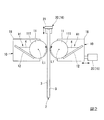
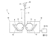
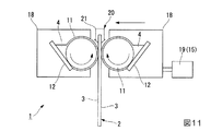
図1〜3に示すように、本実施形態に係る塗布装置1は、基板2の塗布面3に感光性樹脂からなるインク4を塗布する装置である。
対象の基板2は、少なくとも塗布面3に導体回路が形成されているものであれば、任意に構成されてよい。本実施形態の基板2は、その両面(両方の塗布面3,3)に導体回路が形成され、両方の塗布面3,3にソルダーレジストを形成することで、FCBGA(Flip Chip Ball Grid Array)基板等のように両面にバンプが現れる両面印刷回路基板を構成するものである。
塗布装置1は、塗布ロール11と、ドクターバー12と、ロール回転駆動部13と、ドクターバー駆動部14と、ロール押込み駆動部15と、移送部16と、制御部17と、を備える。
Hereinafter, the details of the present invention will be described based on the embodiments.
As shown in FIGS. 1 to 3, the
The
The
塗布ロール11は、円柱状に形成され、基板2の塗布面3に対向する周面111を有する。塗布ロール11の周面111には、インク4が塗布される。塗布ロール11は、その軸線L1を中心に回転できるように、また、塗布ロール11の周面111を基板2の塗布面3に押し付けることができるように、塗布装置1のベース(不図示)に設けられている。塗布ロール11は、ウレタンゴム等のように弾性変形可能な弾性体である。
本実施形態において、塗布ロール11は、基板2の両方の塗布面3,3に対向し、基板2をその厚さ方向から挟み込むことができるように、基板2の厚さ方向に間隔をあけて一対配列されている。
The
In the present embodiment, the coating rolls 11 face both
一対の塗布ロール11,11は、相対的に近づいたり離れたりする方向に移動するように、塗布装置1のベースに設けられている。これにより、各塗布ロール11の周面111を基板2の各塗布面3に押し付けることができる。一対の塗布ロール11,11は、例えば、基板2の各塗布面3に対して近づいたり離れたりする方向に各々移動可能となるように、塗布装置1のベースに設けられてもよい。本実施形態では、一対の塗布ロール11,11のうち一方(図2において右側の塗布ロール11)が、基板2の塗布面3に対して近づいたり離れたりするように、塗布装置1のベースに対して移動可能に設けられている。他方の塗布ロール11は、塗布装置1のベースに対して移動しないように設けられている。
The pair of coating rolls 11 and 11 are provided on the base of the
ドクターバー12は、概ね平板状に形成され、各塗布ロール11の周面111に押し付けられる。より具体的に、ドクターバー12は、基板2との間に塗布ロール11が位置するように配されている。図2のように塗布ロール11の軸線L1方向から見て、鉛直方向(図1,2において上下方向)におけるドクターバー12の下端部は、塗布ロール11の周面111に対して最も近くに位置する。ドクターバー12の下端部は塗布ロール11の周面111に押し付けられる。ドクターバー12は、その下端部から上端部に向かうにしたがって塗布ロール11の周面111から離れるように延びている。ドクターバー12は、塗布ロール11に対する押し付け圧力が変化するように、塗布ロール11に対して移動可能とされている。
インク4を塗布ロール11の周面111に供給するためにインク4を貯留する貯留空間V1は、例えば別途設けられてもよいが、本実施形態では、塗布ロール11とドクターバー12との隙間によって形成されている。
The
A storage space V1 for storing the
本実施形態において、各塗布ロール11及び各塗布ロール11に対応するドクターバー12は、同一の支持体18によって支持されている。支持体18は、塗布ロール11の軸線L1方向における塗布ロール11及びドクターバー12の両端部を支持する。
本実施形態では、一方の塗布ロール11が基板2の塗布面3に対して近づいたり離れたりするように、一方の塗布ロール11及びドクターバー12を支持する一方の支持体18(図2において右側の支持体18)が、塗布装置1のベースに対して移動可能とされている。他方の塗布ロール11及びドクターバー12を支持する他方の支持体18は、塗布装置1のベースに固定されている。
In this embodiment, each
In the present embodiment, one
ロール回転駆動部13は、各塗布ロール11を回転駆動する。ロール回転駆動部13には、任意のモータが採用されてよいが、本実施形態では塗布ロール11の回転角度や回転速度を把握できるように、入力されたパルス信号によって動作するパルスモータが採用されている。
The roll
ドクターバー駆動部14は、ドクターバー12を駆動してドクターバー12を塗布ロール11の周面111に対して押し当てたり、離脱させたりする。また、ドクターバー駆動部14は、ドクターバー12を駆動して各塗布ロール11に対するドクターバー12(特にドクターバー12の下端部)の押し込み量を変化させる。
ここで、ドクターバー12の押し込み量は、塗布ロール11に対する押し付け圧力が変化するようにドクターバー12が塗布ロール11に対して移動する移動長さである。ドクターバー12の押し込み量は、塗布ロール11の周面111に塗布されたインク4がドクターバー12によって掻き取られた後に塗布ロール11の周面111に残るインク4の膜厚に関係する。例えばドクターバー12の押し込み量が増加した場合、塗布ロール11の周面111におけるインク4の膜厚は減少する。
ドクターバー駆動部14には、任意のモータが採用されてよいが、本実施形態ではドクターバー12の押し込み量を把握できるように、入力されたパルス信号によって動作するパルスモータが採用されている。
The doctor
Here, the pushing amount of the
An arbitrary motor may be adopted for the doctor
ロール押込み駆動部15は、塗布ロール11を駆動して塗布面3に対する塗布ロール11の押し込み量を変化させる。より具体的に、ロール押込み駆動部15は、塗布ロール11を基板2の塗布面3に対して近づいたり離れたりする方向に移動させる。ロール押込み駆動部15は、例えば一対の塗布ロール11,11をそれぞれ駆動してもよいが、本実施形態では一方の塗布ロール11のみを駆動する。また、本実施形態のロール押込み駆動部15は、支持体18並びに支持体18に支持された塗布ロール11及びドクターバー12からなる塗布ユニット10を、塗布ロール11が塗布面3に対して近づいたり離れたりする方向に移動させるユニット駆動部19として構成されている。
ユニット駆動部19(ロール押込み駆動部15)には、任意のモータが採用されてよいが、本実施形態では塗布ロール11の押し込み量を把握できるように、入力されたパルス信号によって動作するパルスモータが採用されている。
The roll pushing
An arbitrary motor may be adopted for the unit drive unit 19 (roll push drive unit 15), but in the present embodiment, a pulse motor that operates by an input pulse signal so that the push amount of the
移送部16は、基板2の塗布面3に沿って塗布ロール11及び基板2を相対的に移動させる。移送部16による塗布ロール11と基板2との相対的な移動速度は、少なくとも塗布面3にインク4を塗布する際に、塗布ロール11が基板2の塗布面3上を転がるように、後述する制御部17によって塗布ロール11の回転速度に対応するように制御される。
移送部16は、例えば塗布ロール11を移送するロール移送部であってもよいが、本実施形態では基板2を移送する基板移送部20である。
The
The
本実施形態において、基板移送部20は、一対の塗布ロール11,11の間に基板2を送り込んだり、一対の塗布ロール11,11の間から基板2を引き抜いたりするように、基板2を移送する。
より具体的に説明すれば、基板移送部20は、基板2を保持する保持部21と、保持部21を移動させる移送駆動部22と、を備える。
保持部21は、基板2を吊下げるように基板2の端部を保持し、塗布装置1のベースに対して上下(鉛直方向)に移動可能とされている。
移送駆動部22は、保持部21に保持された基板2が一対の塗布ロール11,11の間を通過するように、保持部21を上下に移動させる。移送駆動部22の駆動系には、パルスモータを使用し、後述する制御部17がモータに指示したパルス量を累積集計することで基板2の位置を把握する。本実施形態ではパルスモータを採用したが、少なくともデジタル量で動作指示が可能な駆動装置であればよく、例えばリニアスライダ等を用いることも可能である。
In the present embodiment, the
More specifically, the
The holding
The
制御部17は、ロール回転駆動部13、ドクターバー駆動部14、ロール押込み駆動部15のうち少なくとも一つの動作を制御し、塗布ロール11の周面111に対するドクターバー12の押し込み量、塗布ロール11の回転速度、基板2の塗布面3に対する塗布ロール11の押し込み量の少なくとも一つを変化させる。
The
本実施形態の塗布装置1は、制御部17が実行する各種処理に用いる各種情報や、制御部17が実行した各種処理によって得られた各種情報を記憶する記憶部23を備える。制御部17は、記憶部23に記憶された各種情報に基づいて、ロール回転駆動部13、ドクターバー駆動部14、ロール押込み駆動部15のうち少なくとも一つの動作を制御する。以下、この点について具体的に説明する。
The
本実施形態の記憶部23には、図4〜6のグラフのように、基板2の塗布面3におけるインク4の膜厚と、ドクターバー12の押し込み量、塗布ロール11の回転速度、塗布ロール11の押し込み量の少なくとも一つと、を対応付けた制御用情報が記憶されている。制御用情報におけるインク4の膜厚は、インク4が基板2の塗布面3に塗布された後に、UVキュア及びポストベーク処理を実施して塗布面3上のインク4をソルダーレジストとした後の膜厚である。また、制御用情報におけるインク4の膜厚は、例えば露光処理、現像処理を実施した後の膜厚としてもよい。
As shown in the graphs of FIGS. 4 to 6, the
図4のグラフは、塗布ロール11に対するドクターバー12の押し込み量と、基板2の塗布面3におけるインク4(ソルダーレジスト)の膜厚とを対応付けた制御用情報であり、ドクターバー12の押し込み量を制御するために用いる。図4の制御用情報では、塗布ロール11の回転速度及び塗布ロール11の押し込み量を一定としている。
図4のグラフでは、塗布ロール11に対するドクターバー12の押し込み量が増加するにしたがって、基板2の塗布面3におけるインク4の膜厚が減少している。これは、ドクターバー12の押し込み量が大きいほど、ドクターバー12によって掻き取られた後に塗布ロール11の周面111に残るインク4の膜厚が小さくなることに起因する。
The graph of FIG. 4 is control information in which the pushing amount of the
In the graph of FIG. 4, the film thickness of the
図5のグラフは、塗布ロール11の回転速度と、基板2の塗布面3におけるインク4(ソルダーレジスト)の膜厚とを対応付けた制御用情報であり、塗布ロール11の回転速度を制御するために用いる。図5の制御用情報では、ドクターバー12の押込み量及び塗布ロール11の押し込み量を一定としている。
図5のグラフでは、塗布ロール11の回転速度が増加するにしたがって、基板2の塗布面3におけるインク4の膜厚が増加している。これは、塗布ロール11の回転速度が大きいほど、塗布ロール11が単位時間あたりにドクターバー12から受ける圧力(線厚)が小さくなることで、ドクターバー12によって掻き取られた後に塗布ロール11の周面111に残るインク4の膜厚が大きくなることに起因する。
The graph of FIG. 5 is control information in which the rotation speed of the
In the graph of FIG. 5, as the rotation speed of the
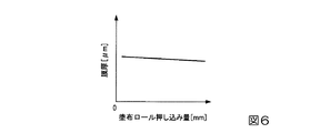
図6のグラフは、基板2の塗布面3に対する塗布ロール11の押し込み量と、基板2の塗布面3におけるインク4(ソルダーレジスト)の膜厚とを対応付けた制御用情報であり、塗布ロール11の回転速度を制御するために用いる。図6の制御用情報では、ドクターバー12の押込み量及び塗布ロール11の回転速度を一定としている。
図6のグラフでは、基板2の塗布面3に対する塗布ロール11の押し込み量が増加するにしたがって、基板2の塗布面3におけるインク4の膜厚が減少している。これは、塗布ロール11の押し込み量が大きいほど、塗布ロール11上のインク4が通り得る基板2の塗布面3と塗布ロール11の周面111との隙間が小さくなることに起因する。
The graph of FIG. 6 is control information in which the pressing amount of the
In the graph of FIG. 6, as the amount of pressing of the
記憶部23には、上記した図4〜6の三つの制御用情報が個別に記憶されてもよいが、例えば、図4〜6の三つのうち二つ選択して組み合わせた制御用情報が記憶されてもよいし、図4〜6の三つ全てを組み合わせた制御用情報が記憶されてもよい。
The three control information of FIGS. 4 to 6 described above may be individually stored in the
制御部17は、上記した制御用情報に基づいて、ロール回転駆動部13、ドクターバー駆動部14、ロール押込み駆動部15のうち少なくとも一つの動作を制御する。これにより、インク4を所望の膜厚で塗布面3に塗布することが可能となる。例えば、塗布装置1を扱う作業者がインク4の膜厚の目標値(目標膜厚)をキーボード等の入力部(不図示)に入力し、制御部17が、制御用情報に基づいて目標膜厚に対応するドクターバー12の押し込み量、塗布ロール11の回転速度、塗布ロール11の押し込み量の少なくとも一つを設定することで、目標膜厚に対応する膜厚でインク4を基板2の塗布面3に塗布できる。
The
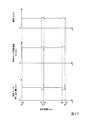
また、本実施形態の記憶部23には、移送部16によって塗布ロール11と基板2とが相対的に移送される方向(移送方向)における基板2の位置と、基板2の塗布面3におけるインク4の複数の目標膜厚と、を対応付けた目標情報が記憶されている。
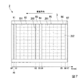
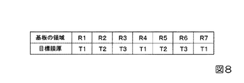
目標情報は、例えば図8に示すように、基板2の塗布面3において基板2の移送方向に並ぶ複数の領域R1〜R7(図7参照)と、各領域R1〜R7におけるインク4の目標膜厚とを対応付けたデータテーブルである。図7において、基板2の移送方向は左方向であり、基板2の塗布面3には、基板2の左端から右方向に向けてインク4が順次塗布される。
Further, in the
As shown in FIG. 8, for example, the target information includes a plurality of regions R1 to R7 (see FIG. 7) arranged in the transfer direction of the
さらに、本実施形態の塗布装置1は、図3に示すように、移送方向における基板2の位置を検出する基板位置検出部30を備える。
制御部17は、記憶部23に記憶された目標情報(図8参照)を参照して基板位置検出部30から出力された基板2の位置に対応するインク4の目標膜厚と、前述した制御用情報(図4〜6参照)に基づいて、ロール回転駆動部13、ドクターバー駆動部14、ロール押込み駆動部15のうち少なくとも一つの動作を制御する。これにより、移送方向における基板2の位置に応じて、塗布面3におけるインク4の膜厚を適宜変化させることができる。
Further, as shown in FIG. 3, the
The
上記した基板位置検出部30は、例えば、押付検知センサ31と、速度検出センサ32と、位置算出部34と、を備えてよい。
押付検知センサ31は、基板2に対する塗布ロール11の押し付けを検知する。押付検知センサ31は、例えば塗布ロールに設けられる圧力センサによって構成されてもよいが、例えばパルスモータからなるユニット駆動部19(ロール押込み駆動部15)によって構成されてもよい。
速度検出センサ32は、基板2の塗布面3上で転がる塗布ロール11の回転速度を検出する。速度検出センサ32は、例えば塗布ロール11の回転速度を直接検出するセンサによって構成されてもよいが、例えばパルスモータからなるロール回転駆動部13によって構成されてもよい。
The substrate
The
The
位置算出部34は、押付検知センサ31において検知された検知情報に基づいて、基板2の塗布面3に対してインク4の塗布が開始された塗布開始位置を設定する。さらに、位置算出部34は、塗布開始位置を基準として、速度検出センサ32において検出された塗布ロール11の回転速度に基づいて、移送方向における基板2の位置を継続的に算出する。位置算出部34は、例えば制御部17に含まれてもよい。
The
また、上記した基板位置検出部30は、例えば、移送部16による塗布ロール11と基板2との相対的な移送距離を検出する距離検出センサ33を備えてもよい。
この場合、位置算出部34は、前述と同様に、基板2の塗布面3に対してインク4の塗布が開始された塗布開始位置を設定した上で、塗布開始位置を基準として、距離検出センサ33において検出された移送距離に基づいて、移送方向における基板2の位置を継続的に算出する。
基板位置検出部30は、上記した速度検出センサ32及び距離検出センサ33の両方を備えてもよいが、例えば一方のみ備えてもよい。
Further, the substrate
In this case, the
The substrate
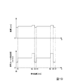
位置算出部34において設定される塗布開始位置は、例えば、基板2の塗布面3に対する塗布ロール11の押し付け開始時において、塗布面3におけるインク4の膜厚の変動の大きさが許容範囲内となる位置に設定されるとよい。
位置算出部34において設定される塗布開始位置は、例えば図7,9に示すように、基板2の移送方向において塗布ロール11が押し付けられる基板2の位置XPとしてもよい。例えば、塗布ロール11を基板2に押し付けた直後における塗布膜厚(塗布面3におけるインク4の膜厚)が安定している場合、また、ドクターバー12の押し込み量、塗布ロール11の回転速度、塗布ロール11の押し込み量の少なくとも一つを制御することで、塗布ロール11を基板2に押し付けた直後における塗布膜厚を安定させる場合には、塗布開始位置を基板2の位置XPとしてもよい。
The coating start position set by the
The coating start position set by the
また、例えば、塗布ロール11が基板2に押し付けられた基板2の位置XPから基板2の移送方向に所定距離D2だけ進むまで塗布膜厚が安定しない場合、位置算出部34において設定される塗布開始位置は、例えば、基板2の位置XPから所定距離D2だけ進んだ基板2の位置X0としてもよい。
所定距離D2は、例えば塗布装置1で試験を実施し、塗布ロール11を押し付けた位置XPから塗布膜厚が安定するまでの距離を測定することで得てもよい。また、所定距離D2は、例えば図9に示すように、塗布ロール11の回転方向において、ドクターバー12が押し付けられる塗布ロール11の周面111の第一位置P1から、基板2の塗布面3に押し付けられる塗布ロール11の周面111の第二位置P2に至る周面111上の距離D1(=2πr×θ/360°)以上としてもよい。
また、所定距離D2は、例えば、塗布ロール11を基板2に押し付ける際にドクターバー12の押し込み量、塗布ロール11の回転速度、塗布ロール11の押し込み量の少なくとも一つを制御して塗布膜厚を安定させる等することで、距離D1よりも短く設定されてもよい。
Further, for example, when the coating film thickness is not stable until the
The predetermined distance D2 may be obtained, for example, by conducting a test with the
Further, the predetermined distance D2 controls, for example, at least one of the pushing amount of the
次に、本実施形態に係るインク4の塗布方法について説明する。
Next, the method of applying the
本実施形態のインク4の塗布方法では、回転する塗布ロール11の周面111に塗布されたインク4を、塗布ロール11の周面111に押し付けられたドクターバー12によって掻き取ることで、インク4を所定の厚みで塗布ロール11の周面111に塗布させる。また、回転する塗布ロール11を基板2の塗布面3に押し込むことで、インク4を基板2の塗布面3に塗布する。
そして、本実施形態のインク4の塗布方法では、塗布ロール11の周面111に対するドクターバー12の押し込み量、塗布ロール11の回転速度、塗布ロール11の押し込み量の少なくとも一つを変化させる。
以下、本実施形態の塗布装置1を用いたインク4の塗布方法について、より具体的に説明する。
In the method of applying the
Then, in the method of applying the
Hereinafter, the method of applying the
まず、基板2の塗布面3にインク4を塗布する手順を説明する。
基板2の塗布面3にインク4を塗布する際には、はじめに、図11に示すように、移送方向における基板2の第一端部を一対の塗布ロール11,11の間に位置させる準備工程を実施する。準備工程では、図10に示すように、基板2を基板移送部20の保持部21に保持させた状態で、基板移送部20によって基板2を下降させて図11に示す位置まで移動させればよい。準備工程においては、例えば、保持部21が一対の塗布ロール11,11よりも下側で基板2を保持した後、基板2が一対の塗布ロール11,11の間を通過するように基板2を上昇させて図11に示す位置まで移動してもよい。さらに、塗布ロール11は、準備工程において塗工準備が完了した段階で回転してもよいが、後述する押付工程を実施するまで停止していてもよい。
First, a procedure for applying the
When applying the
上記した準備工程を完了した後には、図11に示すように、一対の塗布ロール11,11によって一対の基板2をその厚さ方向から挟み込み、各塗布ロール11を回転させながら各塗布面3に押し付ける押付工程を実施し、塗布動作を開始する。
押付工程では、一方の塗布ロール11(図11において右側の塗布ロール11)が他方の塗布ロール11に近づくように、ロール押込み駆動部15(ユニット駆動部19)によって一方の塗布ロール11を移動させればよい。押付工程を実施することで、一対の塗布ロール11,11が基板2の各塗布面3に押し込まれる。
前述した準備工程において塗布ロール11の回転が停止している場合、押付工程では、各塗布ロール11を周面111上の距離D1に対応する角度θ(図9参照)以上に回転(空転)させた上で、各塗布ロール11を基板2の各塗布面3に押し付けるとよい。これにより、塗布ロール11を基板2の塗布面3に押し付けた時点から塗布面3に対するインク4の塗布を開始できる。
After completing the above-mentioned preparatory steps, as shown in FIG. 11, the pair of
In the pressing step, one
When the rotation of the
その後、図12に示すように、基板移送部20によって基板2を移送方向に移送する移送工程を実施する。移送工程では、各塗布ロール11が基板2の各塗布面3上を転がるように、基板移送部20による基板2の移送速度を、塗布ロール11の回転速度に対応させる。移送工程を実施することで、移送方向における基板2の第一端部から第二端部に向けて基板2の各塗布面3にインク4が塗布される。
そして、図13に示すように、基板2の第二端部が一対の塗布ロール11,11の間に到達することで、基板2の塗布面3に対するインク4の塗布が完了する。
上記したインク4の塗布において、塗布ロール11の回転、保持部21の移動等は、制御部17がロール回転駆動部13や移送駆動部22等の動作を制御することで行われる。
After that, as shown in FIG. 12, a transfer step of transferring the
Then, as shown in FIG. 13, when the second end portion of the
In the above-mentioned coating of the
そして、本実施形態のインク4の塗布方法では、前述の移送工程において、制御部17が、ドクターバー駆動部14、ロール回転駆動部13、ロール押込み駆動部15のうち少なくとも一つの動作を制御して、ドクターバー12の押し込み量、塗布ロール11の回転速度、塗布ロール11の押し込み量の少なくとも一つを変化させる。より具体的に、本実施形態のインク4の塗布方法では、移送方向における基板2の塗布面3の途中の位置(所定位置)で、ドクターバー12の押し込み量、塗布ロール11の回転速度、塗布ロール11の押し込み量の少なくとも一つを変化させる。
ドクターバー12の押し込み量、塗布ロール11の回転速度、塗布ロール11の押し込み量の少なくとも一つを変化させることで、図4〜6に示したように、基板2の塗布面3に塗布されるインク4の膜厚を変えることができる。
Then, in the
By changing at least one of the pushing amount of the
上記したインク4の塗布方法では、例えば基板2の塗布面3にインク4を塗布する工程(特に押付工程及び移送工程)が1回のみ実施されてもよいが、例えば複数回繰り返して実施されてもよい。
この場合、基板2の塗布面3上にインク4を塗布した後、UVキュア及びポストベーク処理を実施した後に、再度、基板2の塗布面3上にインク4を塗布すればよい。また、基板2の塗布面3に所定の開口パターンを有するソルダーレジストを形成する場合には、UVキュア及びポストベーク処理を実施する前に、露光処理、現像処理を実施してもよい。
In the above-described
In this case, after applying the
本実施形態の塗布装置1及びインク4の塗布方法によれば、インク4を基板2の塗布面3に塗布している間に、基板2の塗布面3に塗布されるインク4の膜厚を変えることができる。したがって、同一の基板2上でソルダーレジストの膜厚が異なる複数種類の回路基板の製造が可能となる。することができる。その結果として、複数種類の回路基板の製造に要する作業時間を短縮できると共に、基板、ソルダーレジストの材料の使用量を低減できるという効果が得られる。
According to the
以下、本発明を実施例によりさらに具体的に説明するが、本発明はこれらの実施例により限定されるものではない。 Hereinafter, the present invention will be described in more detail with reference to Examples, but the present invention is not limited to these Examples.
[基板]
本実施例では、基板2として、ガラスエポキシの板材(ガラスエポキシ板)の両面に銅材からなる導体回路を形成した両面基板を用意した。ガラスエポキシ板の各寸法は、縦612mm、横512mm、厚さ0.8mmとした。ガラスエポキシ板の縦寸法は、基板2の移送方向に対応する寸法とした。ガラスエポキシ板の横寸法は、基板2の移送方向及び厚さ方向に直交する方向の寸法とした。導体回路は、ガラスエポキシ板の両面に公知の方法で形成した。
[substrate]
In this embodiment, as the
[インクの塗布方法(ソルダーレジストの形成方法)]
本実施例では、はじめに、基板2に酸洗浄処理及び表面粗化処理を施した。次いで、本実施形態の塗布装置1を用い、基板2の両面(両方の塗布面3,3)にインク4を塗布した。その後、塗布されたインク4に、露光処理及び現像処理を施して所定の開口パターンを形成した。そして、UVキュア及びポストベーク処理を施して、基板2の両面のインク4をソルダーレジストとした。
[Ink application method (solder resist formation method)]
In this embodiment, first, the
本実施例では、図14〜20の各グラフに示すように、7種類のインク4の塗布方法(実施例1〜7)を実施した。
第一の塗布方法(実施例1)では、図14に示すように、ドクターバー12の押し込み量、塗布ロール11の回転速度及び塗布ロール11の押し込み量を変化させることで、インク4の膜厚を変えた。
第二の塗布方法(実施例2)では、図15に示すように、ドクターバー12の押し込み量及び塗布ロール11の回転速度を変化させることで、インク4の膜厚を変えた。実施例2では、塗布ロール11の押し込み量を一定とした。
第三の塗布方法(実施例3)では、図16に示すように、ドクターバー12の押し込み量及び塗布ロール11の押し込み量を変化させることで、インク4の膜厚を変えた。実施例3では、塗布ロール11の回転速度を一定とした。
第四の塗布方法(実施例4)では、図17に示すように、塗布ロール11の回転速度及び塗布ロール11の押し込み量を変化させることで、インク4の膜厚を変えた。実施例4では、ドクターバー12の押し込み量を一定とした。
In this example, as shown in each graph of FIGS. 14 to 20, seven kinds of
In the first coating method (Example 1), as shown in FIG. 14, the film thickness of the
In the second coating method (Example 2), as shown in FIG. 15, the film thickness of the
In the third coating method (Example 3), as shown in FIG. 16, the film thickness of the
In the fourth coating method (Example 4), as shown in FIG. 17, the film thickness of the
第五の塗布方法(実施例5)では、図18に示すように、ドクターバー12の押し込み量を変化させることで、インク4の膜厚を変えた。実施例5では、塗布ロール11の回転速度及び塗布ロール11の押し込み量を一定とした。
第六の塗布方法(実施例6)では、図19に示すように、塗布ロール11の回転速度を変化させることで、インク4の膜厚を変えた。実施例6では、ドクターバー12の押し込み量及び塗布ロール11の押し込み量を一定とした。
第七の塗布方法(実施例7)では、図20に示すように、塗布ロール11の押し込み量を変化させることで、インク4の膜厚を変えた。実施例7では、ドクターバー12の押し込み量及び塗布ロール11の回転速度を一定とした。
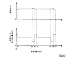
In the fifth coating method (Example 5), as shown in FIG. 18, the film thickness of the
In the sixth coating method (Example 6), as shown in FIG. 19, the film thickness of the
In the seventh coating method (Example 7), as shown in FIG. 20, the film thickness of the
実施例1〜7の塗布方法では、いずれも基板2の塗布面3のうち塗布ロール11が押し付けられた基板2の位置XPから基板2の移送方向に所定距離D2だけ進んだ位置X0を、基板2におけるインク4の塗布開始位置(塗布開始位置X0)とした(図9参照)。
図14〜20に示す各グラフの横軸は、塗布開始位置X0からの塗布距離を示しており、図7に例示した基板2のX軸方向に対応する。
In each of the coating methods of Examples 1 to 7, the substrate is located at the position X0 of the
The horizontal axis of each graph shown in FIGS. 14 to 20 indicates the coating distance from the coating start position X0, and corresponds to the X-axis direction of the
図14〜16,18の各グラフにおいて、ドクターバー12の押し込み量の基準(ゼロ点)は、例えば、塗布ロール11に対するドクターバー12の押し付け圧力がゼロとなるドクターバー12の位置(例えばドクターバー12が塗布ロール11に接触のみしている位置)である。図14〜16,18の各グラフにおける押し込み量の正方向は、塗布ロール11に対するドクターバー12の押し付け圧力が増加することを意味する。
In each of the
図14,16,17,20の各グラフにおいて、塗布ロール11の押し込み量の基準(ゼロ点)は、例えば、基板2の塗布面3に対する塗布ロール11の押し付け圧力がゼロとなる塗布ロール11の位置(例えば塗布ロール11が基板2に接触のみしている塗布ロール11の位置)である。図14,16,17,20の各グラフにおける塗布ロール11の押し込み量の正方向は、基板2の塗布面3に対する塗布ロール11の押し付け圧力が増加することを意味する。
In each of the graphs of FIGS. 14, 16, 17, and 20, the reference (zero point) of the pressing amount of the
実施例1〜7では、いずれも図7に示す基板2の塗布面3の各領域R1〜R7におけるインク4の各目標膜厚T1,T2,T3(図8参照)を以下のように設定した。
目標膜厚T1=12μm
目標膜厚T2=14μm
目標膜厚T3=16μm
各領域R1〜R7におけるインク4の目標膜厚T1,T2,T3は、基板2の両方の塗布面3,3で同じとした。
In Examples 1 to 7, each target film thickness T1, T2, T3 (see FIG. 8) of the
Target film thickness T1 = 12 μm
Target film thickness T2 = 14 μm
Target film thickness T3 = 16 μm
The target film thicknesses T1, T2, and T3 of the
実施例1〜7では、図7の基板2及び図14〜20のグラフに示すように、いずれもインク4を塗布面3に塗布する際に、以下の手順でインク4の膜厚を変えた。
はじめに、塗布面3の領域R1と領域R2との境界となる基板2の位置X1で、ドクターバー12の押し込み量を減少させたり、塗布ロール11の回転速度を増加させたり、塗布ロール11の押し込み量を減少させたりすることで、基板2の塗布面3に塗布されるインク4の膜厚を増加させた。
次いで、塗布面3の領域R2と領域R3との境界となる基板2の位置X2で、ドクターバー12の押し込み量をさらに減少させたり、や塗布ロール11の回転速度をさらに増加させたり、塗布ロール11の押し込み量をさらに減少させたりすることで、基板2の塗布面3に塗布されるインク4の膜厚をさらに増加させた。
In Examples 1 to 7, as shown in the
First, at the position X1 of the
Next, at the position X2 of the
その後、塗布面3の領域R3と領域R4との境界となる基板2の位置X3で、ドクターバー12の押し込み量を増加させたり、塗布ロール11の回転速度を減少させたり、塗布ロール11の押し込み量を増加させたりすることで、基板2の塗布面3に塗布されるインク4の膜厚を減少させた。
そして、塗布面3の領域R4と領域R5との境界となる基板2の位置X4で、基板2の位置X1の場合と同様に、ドクターバー12の押し込み量や塗布ロール11の回転速度、塗布ロール11の押し込み量を設定し、領域R5に塗布されるインク4の膜厚を領域R2の場合と同等とした。
After that, at the position X3 of the
Then, at the position X4 of the
さらに、塗布面3の領域R5と領域R6との境界となる基板2の位置X5で、基板2の位置X2の場合と同様に、ドクターバー12の押し込み量や塗布ロール11の回転速度、塗布ロール11の押し込み量を設定し、領域R6に塗布されるインク4の膜厚を領域R3の場合と同等とした。
また、塗布面3の領域R6と領域R7との境界となる基板2の位置X6で、基板2の位置X3の場合と同様に、ドクターバー12の押し込み量や塗布ロール11の回転速度、塗布ロール11の押し込み量を設定することで、領域R7に塗布されるインク4の膜厚を領域R4の場合と同等とした。
最後に、塗布面3の領域R7の端をなす基板2の位置X7で、塗布面3に対するインク4の塗布を終了した。
Further, at the position X5 of the
Further, at the position X6 of the
Finally, the application of the
実施例1〜7では、いずれも目標膜厚T2に設定した塗布面3の領域R2,R5に対応する基板2の部分を、第一回路基板201として製造される部分とした。第一回路基板201は、図7において破線で囲まれた部分とし、各領域R2,R5において複数設けられるようにした。
また、目標膜厚T3に設定した塗布面3の領域R3,R6に対応する基板2の部分を、第二回路基板202として製造される部分とした。第二回路基板202は、図7において破線で囲まれた部分とし、各領域R3,R6において複数設けられるようにした。
目標膜厚T1に設定した塗布面3の領域R1,R4,R7に対応する基板2の部分は、回路基板として製造されない部分とした。領域R1,R4,R7における目標膜厚T1を、領域R2,R3,R5,R6における目標膜厚T2,T3よりも薄く設定して塗布することができるので、従来のように均一な厚みでインク4を塗布する場合と比較して、回路基板201,202を含む基板2に塗布するインク4の量の低減が可能となった。
In Examples 1 to 7, the portion of the
Further, the portion of the
The portion of the
[インク(ソルダーレジスト)の膜厚の測定]
上記した実施例1〜7の各塗布方法で塗布されたインク4の膜厚を測定した。測定されるインク4の膜厚は、インク4を基板2の両方の塗布面3,3に塗布した直後の膜厚ではなく、インク4が基板2の両方の塗布面3,3に塗布された後、UVキュア及びポストベーク処理を実施して各塗布面3上のインク4をソルダーレジストとした後の膜厚とした。また、インク4の膜厚は、例えば露光処理、現像処理を実施した後の膜厚としてもよい。
インク4(ソルダーレジスト)の膜厚は、レーザー顕微鏡を用い、インク4(ソルダーレジスト)に形成された所定の開口パターンにおいて測定した。
図14〜20の各グラフには、移送方向における基板2の位置(塗布開始位置X0を基準とした塗布距離)と、上記の測定方法で測定されたインク4の膜厚との関係を記載した。基板2の位置に対するインク4の膜厚の変化の傾向は、基板2の両方の塗布面3,3で差異が無いため、図14〜20のグラフには、基板2の一方の塗布面3における基板2の位置とインク4の膜厚との関係のみ記載した。
[Measurement of ink (solder resist) film thickness]
The film thickness of the
The film thickness of the ink 4 (solder resist) was measured using a laser microscope in a predetermined aperture pattern formed on the ink 4 (solder resist).
In each graph of FIGS. 14 to 20, the relationship between the position of the
[実施例1〜7の評価]
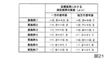
実施例1〜7の各塗布方法で塗布されたインク4の膜厚に関し、インク4の目標膜厚と測定膜厚の誤差を調べた結果を図21に示す。図21において、「一方の塗布面」の欄には、ユニット駆動部19によって駆動される一方の塗布ロール11が押し付けられる基板2の塗布面3におけるインク4の目標膜厚と測定膜厚の誤差を記載した。「他方の塗布面」の欄には、ユニット駆動部19によって駆動されない他方の塗布ロール11が押し付けられる基板2の塗布面3におけるインク4の目標膜厚と測定膜厚の誤差を記載した。インク4の目標膜厚に対する測定膜厚の誤差は、測定膜厚が目標膜厚よりも大きい場合に「+」で示し、測定膜厚が目標膜厚よりも小さいに場合に「−」で示した。
図21に示すように、実施例1〜7では、いずれもインク4の目標膜厚に対する測定膜厚の誤差が最大で1.9μmであった。すなわち、実施例1〜7では、いずれも目標膜厚に近い膜厚でインク4を塗布できることが確認された。これにより、同一の基板2を用いてソルダーレジスト(インク4)の膜厚が異なる二種類の回路基板201,202を製造できることが確認された。
[Evaluation of Examples 1 to 7]
FIG. 21 shows the results of examining the error between the target film thickness of the
As shown in FIG. 21, in each of Examples 1 to 7, the error of the measured film thickness with respect to the target film thickness of the
また、ドクターバー12の押し込み量を一定とした実施例4,6,7では、インク4の目標膜厚に対するインク4の膜厚の誤差の最大値が、いずれも1.4μm以上であった。これに対し、ドクターバー12の押し込み量を変化させた実施例1〜3,5では、インク4の目標膜厚に対するインク4の膜厚の誤差の最大値が、いずれも1.3μm以下であった。したがって、本実施形態の塗布装置1及びインク4の塗布方法によってインク4を基板2の塗布面3に塗布する場合には、ドクターバー12の押し込み量を変化させることで、インク4を高い膜厚精度で基板2に塗布することができることが確認された。
Further, in Examples 4, 6 and 7 in which the pushing amount of the
また、図14〜20のグラフを見ると、ドクターバー12の押し込み量を変化させた実施例1〜3,5では、ドクターバー12の押し込み量を一定とした実施例4,6,7と比べて、インク4の膜厚が大きく変わることが確認された。すなわち、ドクターバー12の押し込み量を変化させることは、塗布ロール11の回転速度や塗布ロール11の押し込み量を変化させることよりも、インク4の膜厚の変化に大きく寄与することが確認された。したがって、ドクターバー12の押し込み量を変化させることにより、同一の基板2を用いて、インク4(ソルダーレジスト)の膜厚が大きく異なる複数種類の回路基板を製造できることが確認された。
Further, looking at the graphs of FIGS. 14 to 20, in Examples 1 to 3 and 5 in which the pushing amount of the
以上、本発明について詳細に説明したが、本発明は上記実施形態に限定されるものではなく、本発明の趣旨を逸脱しない範囲において種々の変更を加えることが可能である。 Although the present invention has been described in detail above, the present invention is not limited to the above-described embodiment, and various modifications can be made without departing from the spirit of the present invention.
本発明の塗布装置は、インクを基板の両方の塗布面に塗布するように構成されることに限らず、例えば基板の一方の塗布面のみに塗布するように構成されてもよい。すなわち、本発明の塗布装置は、少なくとも一つの塗布ロールを備えればよい。また、本発明のインクの塗布方法では、同様にして、少なくともインクを基板の一方の塗布面に塗布すればよい。 The coating apparatus of the present invention is not limited to being configured to apply ink to both coated surfaces of the substrate, and may be configured to be applied to, for example, only one coated surface of the substrate. That is, the coating apparatus of the present invention may include at least one coating roll. Further, in the ink application method of the present invention, at least the ink may be applied to one of the coated surfaces of the substrate in the same manner.
また、例えば、塗布装置の制御部や位置算出部の機能を実現するためのプログラムをコンピュータ読み取り可能な記録媒体に記録して、この記録媒体に記録されたプログラムをコンピュータシステムに読み込ませ、実行することにより、制御部や位置算出部が実行する処理を行ってもよい。なお、ここでいう「コンピュータシステム」とは、OSや周辺機器等のハードウェアを含むものであってもよい。 Further, for example, a program for realizing the functions of the control unit and the position calculation unit of the coating device is recorded on a computer-readable recording medium, and the program recorded on the recording medium is read and executed by the computer system. As a result, the processing executed by the control unit or the position calculation unit may be performed. The "computer system" referred to here may include hardware such as an OS and peripheral devices.
また、「コンピュータシステム」は、コンピュータネットワークシステムを利用している場合であれば、ホームページ提供環境(あるいは表示環境)も含むものとする。また、「コンピュータ読み取り可能な記録媒体」とは、フレキシブルディスク、光磁気ディスク、フラッシュメモリ等の書き込み可能な不揮発性メモリ、ROM、CD−ROM等の可搬媒体、コンピュータシステムに内蔵されるハードディスク等の記憶装置のことをいう。 In addition, the "computer system" shall also include a homepage providing environment (or display environment) if a computer network system is used. The "computer-readable recording medium" includes a flexible disk, a magneto-optical disk, a writable non-volatile memory such as a flash memory, a portable medium such as a ROM and a CD-ROM, a hard disk built in a computer system, and the like. It refers to the storage device of.
さらに「コンピュータ読み取り可能な記録媒体」とは、インターネット等のネットワークや電話回線等の通信回線を介してプログラムが送信された場合のサーバやクライアントとなるコンピュータシステム内部の揮発性メモリ(例えばDRAM(Dynamic Random Access Memory))のように、一定時間プログラムを保持しているものも含むものとする。
また、上記プログラムは、このプログラムを記憶装置等に格納したコンピュータシステムから、伝送媒体を介して、あるいは、伝送媒体中の伝送波により他のコンピュータシステムに伝送されてもよい。ここで、プログラムを伝送する「伝送媒体」は、インターネット等のネットワーク(通信網)や電話回線等の通信回線(通信線)のように情報を伝送する機能を有する媒体のことをいう。
また、上記プログラムは、前述した機能の一部を実現するためのものであっても良い。
さらに、前述した機能をコンピュータシステムにすでに記録されているプログラムとの組み合わせで実現できるもの、いわゆる差分ファイル(差分プログラム)であっても良い。
Furthermore, the "computer-readable recording medium" is a volatile memory inside a computer system that serves as a server or client when a program is transmitted via a network such as the Internet or a communication line such as a telephone line (for example, DRAM (Dynamic)). It also includes those that hold the program for a certain period of time, such as Random Access Memory)).
Further, the program may be transmitted from a computer system in which this program is stored in a storage device or the like to another computer system via a transmission medium or by a transmission wave in the transmission medium. Here, the "transmission medium" for transmitting a program refers to a medium having a function of transmitting information, such as a network (communication network) such as the Internet or a communication line (communication line) such as a telephone line.
Further, the above program may be for realizing a part of the above-mentioned functions.
Further, a so-called difference file (difference program) may be used, which can realize the above-mentioned functions in combination with a program already recorded in the computer system.
1 塗布装置
2 基板
3 塗布面
4 インク
10 塗布ユニット
11 塗布ロール
12 ドクターバー
13 ロール回転駆動部
14 ドクターバー駆動部
15 ロール押込み駆動部
16 移送部
17 制御部
18 支持体
19 ユニット駆動部
20 基板移送部
21 保持部
22 移送駆動部
23 記憶部
30 基板位置検出部
31 押付検知センサ
32 速度検出センサ
33 距離検出センサ
34 位置算出部
1
Claims (5)
前記塗布面に対向する周面を有し、弾性変形可能な弾性体である塗布ロールと、
前記塗布ロールの周面に押し付けられるドクターバーと、
前記塗布ロールを回転駆動するロール回転駆動部と、
前記ドクターバーを駆動して前記塗布ロールの周面に対する前記ドクターバーの押し込み量を変化させるドクターバー駆動部と、
前記塗布ロールを駆動して前記塗布面に対する前記塗布ロールの押し込み量を変化させるロール押込み駆動部と、
前記ロール回転駆動部、前記ドクターバー駆動部、前記ロール押込み駆動部のうち少なくとも前記ロール押込み駆動部の動作を制御して、前記塗布ロールの周面に対する前記ドクターバーの押し込み量、前記塗布ロールの回転速度、前記塗布面に対する前記塗布ロールの押し込み量のうち少なくとも前記塗布ロールの押し込み量を変化させることで、前記塗布面における前記インクの膜厚を変える制御部と、
を備える塗布装置。 A coating device that applies ink made of photosensitive resin to the coated surface of a substrate.
Have a circumferential surface facing the coating surface, a coating roll is elastically deformable elastic body,
A doctor bar pressed against the peripheral surface of the coating roll and
A roll rotation drive unit that rotationally drives the coating roll,
A doctor bar driving unit that drives the doctor bar to change the pushing amount of the doctor bar with respect to the peripheral surface of the coating roll.
A roll pushing drive unit that drives the coating roll to change the pushing amount of the coating roll with respect to the coated surface.
By controlling the operation of at least the roll pushing drive unit of the roll rotation driving unit, the doctor bar driving unit, and the roll pushing driving unit , the amount of pushing the doctor bar with respect to the peripheral surface of the coating roll and the amount of the doctor bar pushed into the coating roll rotational speed, by changing at least push-in amount of the coating roll of the push-in amount of the coating roll with respect to the coated surface, and a control unit for changing the thickness of the ink on the coating surface,
A coating device comprising.
前記制御部は、前記記憶部に記憶された前記制御用情報に基づいて、前記ロール回転駆動部、前記ドクターバー駆動部、前記ロール押込み駆動部のうち少なくとも前記ロール押込み駆動部の動作を制御する請求項1に記載の塗布装置。 Control information in which the film thickness of the ink on the coating surface, the pushing amount of the doctor bar, the rotation speed of the coating roll, and at least the pushing amount of the coating roll among the pushing amount of the coating roll are associated with each other. Equipped with a memorized storage unit
The control unit controls the operation of at least the roll pushing drive unit among the roll rotation driving unit, the doctor bar driving unit, and the roll pushing drive unit based on the control information stored in the storage unit. The coating apparatus according to claim 1.
前記移送部による移送方向において前記塗布ロールに対する前記基板の位置を検出する基板位置検出部と、
を備え、
前記記憶部には、前記移送方向における前記基板の位置と、前記塗布面における前記インクの膜厚の複数の目標値と、を対応付けた目標情報が記憶され、
前記制御部は、前記基板位置検出部によって検出された前記基板の位置に対応する前記目標値、及び、前記制御用情報に基づいて、前記ロール回転駆動部、前記ドクターバー駆動部、前記ロール押込み駆動部のうち少なくとも前記ロール押込み駆動部の動作を制御する請求項2に記載の塗布装置。 A transfer unit that relatively transfers the coating roll and the substrate along the coating surface so that the coating roll rolls on the coating surface.
A substrate position detection unit that detects the position of the substrate with respect to the coating roll in the transfer direction by the transfer unit.
With
In the storage unit, target information in which the position of the substrate in the transfer direction and a plurality of target values of the ink film thickness on the coated surface are associated with each other is stored.
The control unit has the roll rotation drive unit, the doctor bar drive unit, and the roll push-in unit based on the target value corresponding to the position of the substrate detected by the substrate position detection unit and the control information. The coating device according to claim 2, wherein at least the operation of the roll pushing drive unit is controlled among the drive units.
前記基板に対する前記塗布ロールの押し付けを検出する押付検知センサと、
前記塗布面上で転がる前記塗布ロールの回転速度を検出する速度検出センサと、
前記押付検知センサにおいて検知された検知情報に基づいて、前記塗布面に対してインクの塗布が開始された塗布開始位置を設定し、前記塗布開始位置を基準として、前記速度検出センサにおいて検出された塗布ロールの回転速度に基づいて前記移送方向における前記基板の位置を継続的に算出する位置算出部と、を備える請求項3に記載の塗布装置。 The board position detection unit
A pressing detection sensor that detects the pressing of the coating roll against the substrate, and
A speed detection sensor that detects the rotational speed of the coating roll that rolls on the coating surface, and
Based on the detection information detected by the pressing detection sensor, the coating start position at which ink coating is started is set on the coating surface, and the speed detection sensor detects the ink coating start position as a reference. The coating device according to claim 3, further comprising a position calculation unit that continuously calculates the position of the substrate in the transfer direction based on the rotation speed of the coating roll.
前記塗布ロールは、弾性変形可能な弾性体であり、
前記塗布ロールの周面に対する前記ドクターバーの押し込み量、前記塗布ロールの回転速度、前記塗布面に対する前記塗布ロールの押し込み量のうち少なくとも前記塗布ロールの押し込み量を変化させることで、前記塗布面における前記インクの膜厚を変えるインクの塗布方法。 By scraping the ink applied to the peripheral surface of the rotating coating roll, which is made of a photosensitive resin, with a doctor bar pressed against the peripheral surface of the coating roll, the ink is spread around the coating roll with a predetermined thickness. An ink coating method for applying the ink to the coating surface by pressing the coating roll, which is coated on the surface and rotates, into the coating surface of the substrate.
The coating roll is an elastic body that can be elastically deformed.
By changing at least the pushing amount of the coating roll among the pushing amount of the doctor bar with respect to the peripheral surface of the coating roll, the rotation speed of the coating roll, and the pushing amount of the coating roll with respect to the coating surface, the coating surface thereof. A method of applying an ink that changes the film thickness of the ink.
Priority Applications (1)
| Application Number | Priority Date | Filing Date | Title |
|---|---|---|---|
| JP2016153046A JP6861487B2 (en) | 2016-08-03 | 2016-08-03 | Coating device and ink coating method |
Applications Claiming Priority (1)
| Application Number | Priority Date | Filing Date | Title |
|---|---|---|---|
| JP2016153046A JP6861487B2 (en) | 2016-08-03 | 2016-08-03 | Coating device and ink coating method |
Publications (2)
| Publication Number | Publication Date |
|---|---|
| JP2018020287A JP2018020287A (en) | 2018-02-08 |
| JP6861487B2 true JP6861487B2 (en) | 2021-04-21 |
Family
ID=61165023
Family Applications (1)
| Application Number | Title | Priority Date | Filing Date |
|---|---|---|---|
| JP2016153046A Active JP6861487B2 (en) | 2016-08-03 | 2016-08-03 | Coating device and ink coating method |
Country Status (1)
| Country | Link |
|---|---|
| JP (1) | JP6861487B2 (en) |
Families Citing this family (7)
| Publication number | Priority date | Publication date | Assignee | Title |
|---|---|---|---|---|
| TWI701081B (en) | 2019-12-11 | 2020-08-11 | 群翊工業股份有限公司 | Coating device with thin plate guiding function |
| JP7095900B2 (en) * | 2020-03-11 | 2022-07-05 | 株式会社都ローラー工業 | Coating roll and coating equipment |
| JP7095902B2 (en) * | 2020-04-10 | 2022-07-05 | 株式会社都ローラー工業 | Coating equipment |
| KR102432971B1 (en) * | 2020-03-11 | 2022-08-17 | 카부시키가이샤 미야코 롤러 코교 | Coating apparatus |
| CN116174227B (en) * | 2022-10-08 | 2024-05-17 | 中国一冶集团有限公司 | Construction steel pipe paint painting device and application method thereof |
| CN115846124B (en) * | 2022-12-23 | 2025-07-11 | 华能新能源股份有限公司 | A coating roller scraping system |
| CN119426061B (en) * | 2024-09-02 | 2026-01-02 | 无锡和烁丰新材料有限公司 | A coating process for a non-chemical thermal coated paper |
Family Cites Families (6)
| Publication number | Priority date | Publication date | Assignee | Title |
|---|---|---|---|---|
| JPS48101557A (en) * | 1972-04-07 | 1973-12-20 | ||
| JPH034966A (en) * | 1989-06-01 | 1991-01-10 | Canon Inc | Coating method |
| JP2889128B2 (en) * | 1994-08-31 | 1999-05-10 | 帝人株式会社 | Coating method and device |
| JPH11272082A (en) * | 1998-03-25 | 1999-10-08 | Minolta Co Ltd | Image forming device |
| US20110189378A1 (en) * | 2010-02-04 | 2011-08-04 | Moon So-Ii | Apparatus and method for coating a functional layer |
| JP2015100772A (en) * | 2013-11-27 | 2015-06-04 | 大日本印刷株式会社 | Contact pressure management system, contact pressure management method, coating machine |
-
2016
- 2016-08-03 JP JP2016153046A patent/JP6861487B2/en active Active
Also Published As
| Publication number | Publication date |
|---|---|
| JP2018020287A (en) | 2018-02-08 |
Similar Documents
| Publication | Publication Date | Title |
|---|---|---|
| JP6861487B2 (en) | Coating device and ink coating method | |
| EP3595864B1 (en) | Optical polymer films and methods for casting the same | |
| Rosset et al. | Fabrication process of silicone-based dielectric elastomer actuators | |
| JP2014225669A5 (en) | Substrate holder, lithographic apparatus, and manufacturing method of substrate holder | |
| JP4844729B2 (en) | Nanoimprint method and apparatus | |
| US20170008219A1 (en) | Imprinting apparatus, imprinting method, and method of manufacturing object | |
| JP2015003320A (en) | Coating equipment and coating method | |
| TWI313196B (en) | Method and apparatus for patterning coatings,and method for manufacturing an electronic device | |
| JP7679143B2 (en) | Computer-controlled selective hardening of 3D printed objects | |
| JP2004344916A (en) | Surface processing machine and surface processing method | |
| WO2019026624A1 (en) | Coating mechanism and coating device | |
| KR102946003B1 (en) | Simulation method, storage medium, simulation apparatus, film forming apparatus, and method of manufacturing article | |
| US9527235B2 (en) | Apparatus and method for liquid transfer imprint lithography using a roll stamp | |
| JP2002346448A (en) | Coating apparatus, coating method and release paper manufacturing method | |
| JPH09277144A (en) | Method of printing roll polishing | |
| TWI556987B (en) | Blanket for offset printing and fine pattern manufactured by using the same | |
| JP5884273B2 (en) | Exposure unit and substrate pre-alignment method | |
| US10578424B2 (en) | Rotating/pivoting sensor system for a coordinate measuring apparatus | |
| Koo et al. | Photo‐Thermal Approaches on Polyimide Film for Demonstration of Sub‐50 µm Polymer Stencil Mask | |
| US20070176314A1 (en) | Apparatus for manufacturing display device and method of manufacturing the same | |
| KR102207814B1 (en) | Hand wearable apparatus and manufacturing method for the same | |
| JPH0624771U (en) | Roll coater | |
| JPH01306172A (en) | Method and device for grinding thin film | |
| JP2001154198A5 (en) | ||
| JPS63109974A (en) | Bonding method of substrate |
Legal Events
| Date | Code | Title | Description |
|---|---|---|---|
| A521 | Request for written amendment filed |
Free format text: JAPANESE INTERMEDIATE CODE: A821 Effective date: 20160804 |
|
| RD03 | Notification of appointment of power of attorney |
Free format text: JAPANESE INTERMEDIATE CODE: A7423 Effective date: 20190111 |
|
| A521 | Request for written amendment filed |
Free format text: JAPANESE INTERMEDIATE CODE: A821 Effective date: 20190111 |
|
| A621 | Written request for application examination |
Free format text: JAPANESE INTERMEDIATE CODE: A621 Effective date: 20190709 |
|
| A977 | Report on retrieval |
Free format text: JAPANESE INTERMEDIATE CODE: A971007 Effective date: 20200605 |
|
| A131 | Notification of reasons for refusal |
Free format text: JAPANESE INTERMEDIATE CODE: A131 Effective date: 20200728 |
|
| A521 | Request for written amendment filed |
Free format text: JAPANESE INTERMEDIATE CODE: A523 Effective date: 20200914 |
|
| TRDD | Decision of grant or rejection written | ||
| A01 | Written decision to grant a patent or to grant a registration (utility model) |
Free format text: JAPANESE INTERMEDIATE CODE: A01 Effective date: 20210302 |
|
| A61 | First payment of annual fees (during grant procedure) |
Free format text: JAPANESE INTERMEDIATE CODE: A61 Effective date: 20210330 |
|
| R150 | Certificate of patent or registration of utility model |
Ref document number: 6861487 Country of ref document: JP Free format text: JAPANESE INTERMEDIATE CODE: R150 |
|
| S533 | Written request for registration of change of name |
Free format text: JAPANESE INTERMEDIATE CODE: R313533 |
|
| R350 | Written notification of registration of transfer |
Free format text: JAPANESE INTERMEDIATE CODE: R350 |
|
| R250 | Receipt of annual fees |
Free format text: JAPANESE INTERMEDIATE CODE: R250 |
|
| R250 | Receipt of annual fees |
Free format text: JAPANESE INTERMEDIATE CODE: R250 |
|
| R250 | Receipt of annual fees |
Free format text: JAPANESE INTERMEDIATE CODE: R250 |