JP6855802B2 - Information processing equipment, methods, and programs, D / A converters, electronic musical instruments - Google Patents
Information processing equipment, methods, and programs, D / A converters, electronic musical instruments Download PDFInfo
- Publication number
- JP6855802B2 JP6855802B2 JP2017005427A JP2017005427A JP6855802B2 JP 6855802 B2 JP6855802 B2 JP 6855802B2 JP 2017005427 A JP2017005427 A JP 2017005427A JP 2017005427 A JP2017005427 A JP 2017005427A JP 6855802 B2 JP6855802 B2 JP 6855802B2
- Authority
- JP
- Japan
- Prior art keywords
- signal
- quantization
- output
- pulse
- outputs
- Prior art date
- Legal status (The legal status is an assumption and is not a legal conclusion. Google has not performed a legal analysis and makes no representation as to the accuracy of the status listed.)
- Active
Links
Images


Classifications
-
- H—ELECTRICITY
- H03—ELECTRONIC CIRCUITRY
- H03M—CODING; DECODING; CODE CONVERSION IN GENERAL
- H03M1/00—Analogue/digital conversion; Digital/analogue conversion
- H03M1/12—Analogue/digital converters
- H03M1/50—Analogue/digital converters with intermediate conversion to time interval
- H03M1/52—Input signal integrated with linear return to datum
-
- H—ELECTRICITY
- H03—ELECTRONIC CIRCUITRY
- H03M—CODING; DECODING; CODE CONVERSION IN GENERAL
- H03M3/00—Conversion of analogue values to or from differential modulation
- H03M3/30—Delta-sigma modulation
- H03M3/50—Digital/analogue converters using delta-sigma modulation as an intermediate step
- H03M3/502—Details of the final digital/analogue conversion following the digital delta-sigma modulation
- H03M3/506—Details of the final digital/analogue conversion following the digital delta-sigma modulation the final digital/analogue converter being constituted by a pulse width modulator
-
- G—PHYSICS
- G10—MUSICAL INSTRUMENTS; ACOUSTICS
- G10H—ELECTROPHONIC MUSICAL INSTRUMENTS; INSTRUMENTS IN WHICH THE TONES ARE GENERATED BY ELECTROMECHANICAL MEANS OR ELECTRONIC GENERATORS, OR IN WHICH THE TONES ARE SYNTHESISED FROM A DATA STORE
- G10H1/00—Details of electrophonic musical instruments
- G10H1/32—Constructional details
- G10H1/34—Switch arrangements, e.g. keyboards or mechanical switches specially adapted for electrophonic musical instruments
- G10H1/344—Structural association with individual keys
-
- G—PHYSICS
- G10—MUSICAL INSTRUMENTS; ACOUSTICS
- G10H—ELECTROPHONIC MUSICAL INSTRUMENTS; INSTRUMENTS IN WHICH THE TONES ARE GENERATED BY ELECTROMECHANICAL MEANS OR ELECTRONIC GENERATORS, OR IN WHICH THE TONES ARE SYNTHESISED FROM A DATA STORE
- G10H7/00—Instruments in which the tones are synthesised from a data store, e.g. computer organs
- G10H7/08—Instruments in which the tones are synthesised from a data store, e.g. computer organs by calculating functions or polynomial approximations to evaluate amplitudes at successive sample points of a tone waveform
-
- H—ELECTRICITY
- H03—ELECTRONIC CIRCUITRY
- H03M—CODING; DECODING; CODE CONVERSION IN GENERAL
- H03M3/00—Conversion of analogue values to or from differential modulation
- H03M3/02—Delta modulation, i.e. one-bit differential modulation
-
- H—ELECTRICITY
- H03—ELECTRONIC CIRCUITRY
- H03M—CODING; DECODING; CODE CONVERSION IN GENERAL
- H03M3/00—Conversion of analogue values to or from differential modulation
- H03M3/30—Delta-sigma modulation
- H03M3/39—Structural details of delta-sigma modulators, e.g. incremental delta-sigma modulators
- H03M3/412—Structural details of delta-sigma modulators, e.g. incremental delta-sigma modulators characterised by the number of quantisers and their type and resolution
- H03M3/42—Structural details of delta-sigma modulators, e.g. incremental delta-sigma modulators characterised by the number of quantisers and their type and resolution having multiple quantisers arranged in parallel loops
Description
本発明は、パルス幅変調処理を行う情報処理装置、方法、及びプログラム、D/A変換装置、電子楽器に関する。 The present invention relates to an information processing device, a method, a program, a D / A conversion device, and an electronic musical instrument that perform pulse width modulation processing.
従来より可聴帯域のSN比(信号対雑音比)を向上させるために、量子化ノイズを高域側へシフトさせるノイズシェーピング効果を有するデルタ−シグマ変調器(以下、「ΔΣ変調器」と呼ぶ)を用いたD/A(デジタル−アナログ)変換装置が知られている(例えば特許文献1)。 A delta-sigma modulator (hereinafter referred to as "ΔΣ modulator") having a noise shaping effect that shifts the quantization noise to the high frequency side in order to improve the SN ratio (signal-to-noise ratio) in the audible band. A D / A (digital-analog) converter using the above is known (for example, Patent Document 1).
図10は、従来技術によるΔΣ変調器を用いたD/A変換装置の構成例を示す図である。減算部1004とΣ積分器1001は、デルタ−シグマ変調処理を実行する。量子化器1002は、Σ積分器1001の出力値を量子化する。遅延部1003は、量子化器1002が出力する量子化値をオーバーサンプリングによるサンプリング周期分遅延させる。減算器1004は、デジタル入力値1006から、遅延部1003が出力する値を減算し、減算の結果の値をΣ積分器1001に入力させる。対称パルス幅変調部(以下、「対称PWM部」と呼ぶ)1005は、量子化器1002が出力する量子化値を、その量子化値に対応するデューティ比を有するパルス信号で変調するPWM(Pulse Width Modulation:パルス幅変調)処理を実行し、PWM出力信号1007を出力する。
FIG. 10 is a diagram showing a configuration example of a D / A conversion device using a ΔΣ modulator according to the prior art. The subtraction unit 1004 and the
ここで、上述の従来技術において、図10の減算器1004及びΣ積分器1001でのΔΣ変調処理や対称PWM部1005でのPWM処理は、原信号のサンプリング周期の数十倍以上のオーバーサンプリング周期で動作し、PWMにより生成されるパルス信号の値、すなわち電圧は、時系列的に正確である必要がある。このため、対称PWM部1005で生成されるパルス信号のパルス形状は、必然的にオーバーサンプリング周期毎に、各周期の中心時間位置に対して対称であることが条件となっている。そうしないと、オーバーサンプリング周期の任意の一時点で所望の電圧値が得られず、量子化器1002との整合が保てなくなり、正しい性能が発揮できないためである。図11は、対称PWM部1005でのPWM処理波形の例を示す図である。図11に示される周期Tは、原信号のサンプリング周期Fsを例えば128分割したオーバーサンプリング周期である。図11の例は、図10の量子化器1002が出力する量子化値が例えば−1.0、−0.5、0.0、0.5、1.0の5値を取り得る場合であり、その5値のそれぞれが図11に示される5種類のデューティー比を有するパルス信号にパルス幅変調される。この変調を行うために、オーバーサンプリング周期Tが更に8分割された周期を有する動作クロックCLKに同期して、各量子化値に対応して各パルス信号のデューティー比が制御される。この場合、上述したように、パルス信号のパルス形状は従来、図11に示されるように、オーバーサンプリング周期Tの区間の中心位置T/2に対して左右対称である必要があった。このため、従来のPWMによるパルス信号の分解能(=量子化数)は、オーバーサンプリング周期内での動作クロックCLKの数の約半分に制限されてしまっていた。図11の例では、オーバーサンプリング周期T内での動作クロックCLKのクロック数(周期数)は8周期であり、この場合に変調できる量子化値の数は5値になる。
Here, in the above-mentioned conventional technique, the ΔΣ modulation processing in the subtractor 1004 and the
一方、PWMによるパルス信号の分解能即ち量子化数は、D/A変換装置等のダイナミックレンジに直結するため、ダイナミックレンジを上げるためには、動作クロックの周波数を上げる必要がある。しかして、クロック周波数を上げるためには、より高周波数に対応したPLL(Phased Lock Loop)回路が必要となったり、またそれに伴う消費電力も増加してしまうという課題があった。 On the other hand, since the resolution of the pulse signal by PWM, that is, the number of quantizations, is directly linked to the dynamic range of the D / A conversion device or the like, it is necessary to increase the frequency of the operating clock in order to increase the dynamic range. However, in order to raise the clock frequency, there is a problem that a PLL (Phased Lock Loop) circuit corresponding to a higher frequency is required, and the power consumption associated therewith also increases.
このようなD/A変換装置が例えば電子楽器のアナログ楽音信号の出力用に使用された場合、D/A変換装置のコストアップや消費電力のアップは、電子楽器の性能に直結するため、問題であった。 When such a D / A converter is used, for example, for outputting an analog musical instrument signal of an electronic musical instrument, an increase in the cost and power consumption of the D / A converter is directly linked to the performance of the electronic musical instrument, which is a problem. Met.
そこで、本発明は、動作クロックが同一の場合にはダイナミックレンジを向上させることができ、ダイナミックレンジが同一の場合には動作クロックの周波数を下げて消費電力を抑制できる装置を実現することを目的とする。 Therefore, an object of the present invention is to realize a device capable of improving the dynamic range when the operating clocks are the same and lowering the frequency of the operating clocks when the dynamic ranges are the same to suppress power consumption. And.
態様の一例の情報処理装置は、入力された入力信号と、前記入力信号に基づいて生成された帰還信号との差を積分し、積分結果を出力する積分処理と、前記積分処理により出力された前記積分結果を量子化することにより、第1量子化信号を出力する第1量子化処理と、前記積分処理により出力された前記積分結果を量子化することにより、補正値信号を出力する第2量子化処理と、前記第1量子化信号を第1遅延量で遅延させた第1帰還信号と、前記補正値信号を前記第1遅延量とは異なる第2遅延量で遅延させた第2帰還信号と、を含む前記帰還信号を出力する帰還信号出力処理と、前記第1量子化信号に基づいて、或るクロック周期の中心に対して対称なパルス形状を有するパルス信号と、前記或るクロック周期の中心に対して非対称なパルス形状を有するパルス信号と、を含む出力信号を出力する出力処理と、を実行する処理部を備え、前記第2量子化処理は、前記出力処理により前記対称なパルス形状を有するパルス信号が出力される場合は0とし、前記出力処理により前記非対称なパルス形状を有するパルス信号が出力される場合は、前記パルス信号の中心と前記或るクロック周期の中心との差を補正する補正値を示す信号として前記補正値信号を出力する処理であることを特徴としている。 The information processing device of the embodiment is an integration process that integrates the difference between the input signal and the feedback signal generated based on the input signal and outputs the integration result, and the integration process that outputs the integration result. A first quantization process that outputs a first quantization signal by quantizing the integration result, and a second that outputs a correction value signal by quantizing the integration result output by the integration process. a quantization process, a first feedback signal and the first quantized signal is delayed by a first delay amount, a second feedback delayed by the different second delay amount and the correction value signal said first delay amount signal and a feedback signal output processing for outputting the feedback signal comprising, based on the first quantized signal, a pulse signal having a symmetrical pulse shape with respect to the center of one clock cycle, the certain clock a pulse signal having an asymmetric pulse shape with respect to the center of the period, and an output process for outputting an output signal comprising, Bei example a processor for execution, the second quantization processing, the symmetric by the output processing When a pulse signal having a different pulse shape is output, it is set to 0, and when a pulse signal having an asymmetric pulse shape is output by the output process, the center of the pulse signal and the center of the certain clock period are set. It is characterized in that it is a process of outputting the correction value signal as a signal indicating a correction value for correcting the difference between the above.
本発明によれば、動作クロックが同一の場合にはダイナミックレンジを向上させることができ、ダイナミックレンジが同一の場合には動作クロックの周波数を下げて消費電力を抑制できる装置を実現することが可能となる。 According to the present invention, it is possible to realize a device capable of improving the dynamic range when the operating clocks are the same, and lowering the frequency of the operating clocks when the dynamic ranges are the same to suppress power consumption. It becomes.
以下、本発明を実施するための形態について図面を参照しながら詳細に説明する。本実施形態では、D/A変換装置などの情報処理装置で実行されるPWM処理において、オーバーサンプリング周期等の処理周期毎に、入力値を、入力値に対応するデューティ比を有し、処理周期の中心に対して非対称なパルス形状を含み入力値に対応するパルス形状を有するパルス信号で変調するパルス幅変調処理が実行される。 Hereinafter, embodiments for carrying out the present invention will be described in detail with reference to the drawings. In the present embodiment, in the PWM process executed by an information processing device such as a D / A conversion device, the input value has a duty ratio corresponding to the input value for each processing cycle such as an oversampling cycle, and the processing cycle. A pulse width modulation process that modulates with a pulse signal having a pulse shape that includes a pulse shape that is asymmetric with respect to the center of the input value is executed.
この処理において、パルス信号が非対称なパルス形状を有する場合に、そのパルス信号に基づいて次の処理周期の入力値を補正するための補正値を算出する補正値算出処理が実行される。この補正値算出処理は、処理周期のパルス中心位置を算出すると共に、処理周期の区間中心位置を算出し、算出されたパルス中心位置及び区間中心位置に基づいて補正値を算出する処理である、そして、算出された補正値に基づいて入力値を補正する補正処理が実行される。 In this process, when the pulse signal has an asymmetric pulse shape, a correction value calculation process for calculating a correction value for correcting an input value in the next processing cycle is executed based on the pulse signal. This correction value calculation process is a process of calculating the pulse center position of the processing cycle, calculating the section center position of the processing cycle, and calculating the correction value based on the calculated pulse center position and section center position. Then, a correction process for correcting the input value based on the calculated correction value is executed.
上述の制御処理によって、オーバーサンプリング周期内でその中心に対して非対称なパルス形状を有するパルス信号でパルス幅変調を行うことができるようになり、変調段数をオーバーサンプリング周期内でのPWMのための動作クロックの周期数にほぼ一致させることが可能となって、それによりオーバーサンプリング周期内における量子化段数を増やすことが可能となる。これにより、動作クロックが同一の場合にはダイナミックレンジを向上させることができ、ダイナミックレンジが同一の場合には動作クロックの周波数を下げて消費電力を抑制できる装置を実現することが可能となる。 By the above-mentioned control processing, pulse width modulation can be performed with a pulse signal having a pulse shape asymmetric with respect to the center within the oversampling cycle, and the number of modulation stages can be set for PWM within the oversampling cycle. It is possible to make it substantially match the number of cycles of the operating clock, and thereby it is possible to increase the number of modulation stages in the oversampling cycle. As a result, when the operating clocks are the same, the dynamic range can be improved, and when the dynamic ranges are the same, the frequency of the operating clocks can be lowered to suppress power consumption.
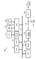
図1は、本発明の一実施形態である電子鍵盤楽器の制御システム100の一実施形態のハードウェア構成例を示す図である。図1において、電子鍵盤楽器の制御システム100は、CPU(中央演算処理装置)101、RAM(ランダムアクセスメモリ)102、ROM(リードオンリーメモリ)103、音源LSI(大規模集積回路)104、鍵盤109とスイッチ部110とが接続されるGPIO(General Purpose Input/Output:汎用入出力)111、及びLCD112が接続されるLCDコントローラ113が、それぞれシステムバス114に接続される構成を備える。また、音源LSI104から出力されるデジタル楽音波形値は、D/Aコンバータ110と、抵抗R 106及び容量C 107とからなるフィルタ部により、アナログ楽音波形信号に変換され、アンプ108で増幅された後に、特には図示しないスピーカ又は出力端子から出力される。
FIG. 1 is a diagram showing a hardware configuration example of an embodiment of a
CPU101は、RAM102をワークメモリとして使用しながらROM103に記憶された制御プログラムを実行することにより、電子鍵盤楽器全体の制御動作を実行する。また、ROM103は、上記制御プログラム及び各種固定データを記憶する。
The
音源LSI104は、波形ROM106から波形を読み出し、D/Aコンバータ110に出力する。音源LSI104は、同時に最大256ボイスを発振させる能力を有する。
The
GPIO111は、鍵盤109とスイッチ部110の操作ボタン状態を定常的に走査し、CPU101に割り込みを掛けて状態変化を伝える。
The
LCDコントローラ113は、LCD112を制御するIC(集積回路)である。
The
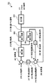
図2は、図1のD/A変換装置105の一実施形態の構成例を示すブロック図である。
FIG. 2 is a block diagram showing a configuration example of an embodiment of the D /
減算器207及びΣ積分器201は、ΔΣ(デルタ−シグマ)変調処理を実行する。
The subtractor 207 and the
第1量子化器202と第2量子化器203はそれぞれ、Σ積分器201が出力する積分結果212を、その値に対応した割合で量子化し、第1量子化信号213及び補正値信号214を出力する。
The
第1遅延部204は、第2量子化器203が出力する補正値信号214をオーバーサンプリング周期分遅延させて、補正値遅延信号215を出力する。
The first delay unit 204 delays the correction value signal 214 output by the
加算器205は、第1量子化器202が出力する第1量子化信号213と第1遅延部204が出力する補正値遅延信号215とを加算し、補正値加算信号216を出力する。
The adder 205 adds the first quantization signal 213 output by the
第2遅延部206は、加算器205が出力する補正値加算信号216をオーバーサンプリング周期分遅延させて、第1帰還信号217を出力する。 The second delay unit 206 delays the correction value addition signal 216 output by the adder 205 by the oversampling cycle, and outputs the first feedback signal 217.
減算器207は、図1の音源LSI205が出力するデジタル楽音波形値210から第2遅延部206がが出力する第1帰還信号217を減算し、その減算の結果得られる値をΣ積分器201に入力させる。
The subtractor 207 subtracts the first feedback signal 217 output by the second delay unit 206 from the digital musical tone shape value 210 output by the sound source LSI 205 of FIG. 1, and transfers the value obtained as a result of the subtraction to the
出力部208は、オーバーサンプリング周期毎に、第1量子化器202が出力する第1量子化信号213に対応するデューティ比を有し、オーバーサンプリング周期の中心に対して非対称なパルス形状を含み第1量子化信号213に応じたパルス形状を有するパルス信号を生成することにより、PWM出力信号211を出力する。
The
このPWM出力信号211は、図1の抵抗R 106及び容量C 107とからなるローパスフィルタ(出力素子)により平滑化され、アナログ楽音波形信号として図1のアンプ108に出力される。
The
図3は、図2のD/A変換装置105が目標とする量子化レベルの例を示す図である。本実施形態では、Σ積分器201の出力値が−1.0、−0.75、−0.50、−0.25、0.00、0.25、0.50、0.75、1.0の9値に量子化される。
FIG. 3 is a diagram showing an example of a quantization level targeted by the D /
これらの量子化値のそれぞれに対して、本実施形態では、出力部208が、量子化値に対応するデューティー比を有し、オーバーサンプリング周期の中心に対して非対称なパルス形状を含み量子化値に応じたパルス形状を有するパルス信号を生成する。
For each of these quantization values, in the present embodiment, the
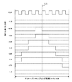
図4は、出力部208でのPWM処理波形の例を示す図である。図11の従来技術の場合と同様に、図4に示される周期Tは、原信号のサンプリング周期Fsを例えば128分割したオーバーサンプリング周期である。図4の例は、目標とする量子化値が前述した9値を取り得る場合であり、その9値のそれぞれが図4に示される9種類のデューティー比を有するパルス信号にパルス幅変調される。この変調を行うために、図11の従来技術の場合と同様に、オーバーサンプリング周期Tが更に8分割された周期を有する動作クロックCLKに同期して、各量子化値に対応して各パルス信号のデューティー比が制御される。
FIG. 4 is a diagram showing an example of a PWM processing waveform in the
この場合、図11の従来技術の場合とは異なり、本実施形態によるパルス信号のパルス形状として、図4に示されるように、オーバーサンプリング周期Tの区間の中心位置T/2に対して左右対称な形状のほかに、左右非対称な形状も採用される。 In this case, unlike the case of the prior art of FIG. 11, the pulse shape of the pulse signal according to the present embodiment is symmetrical with respect to the center position T / 2 of the section of the oversampling period T as shown in FIG. In addition to the various shapes, asymmetrical shapes are also adopted.
この変調制御により、変調段数をオーバーサンプリング周期内でのPWMのための動作クロックの周期数8+1=9とすることが可能となって、図11の場合と同じ動作クロックCLKを用いながら、オーバーサンプリング周期内における量子化段数として、図3に示される9段を達成することが可能となる。図11の場合の変調段数及び量子化段数は4段であったため本実施形態では2倍強の量子化を行うことが可能となる。 This modulation control makes it possible to set the number of modulation stages to 8 + 1 = 9 of the operating clock cycles for PWM within the oversampling cycle, and oversampling while using the same operating clock CLK as in the case of FIG. As the number of quantization stages in the period, it is possible to achieve 9 stages shown in FIG. Since the number of modulation stages and the number of quantization stages in the case of FIG. 11 were four, it is possible to perform quantization of more than twice in this embodiment.
このことは、本実施形態では、従来技術に対して、動作クロックCLKが同一の場合にはダイナミックレンジを2倍強に向上させることができ、ダイナミックレンジを同一とした場合には動作クロックの周波数を1/2弱に下げて消費電力を抑制できることを意味する。 This means that in the present embodiment, the dynamic range can be improved more than twice when the operating clocks CLK are the same, and the frequency of the operating clocks when the dynamic ranges are the same, as compared with the prior art. Means that power consumption can be suppressed by lowering to a little less than 1/2.
図5は、非対称なPWM波形における電圧分割制御を説明する図である。図5(a)に示される対称なPWM波形の場合、平均化した電圧の中心点は、オーバーサンプリング周期Tの中心時間位置bである。本来どのPWMにおけるデューティー比の場合も、各波形の平均かした電圧の中心点がオーバーサンプリング周期内の同じ中心点bにないと、正しい量子化値を表現していることにならない。図5(b)に示される非対称のPWM波形を見てみると、動作クロックCLKの3周期分が電圧のハイレベル区間である。つまり、図5(b)の非対称のPWM波形における平均化した電圧の中心点はa点となり、オーバーサンプリング周期の中心点b点からずれている。 FIG. 5 is a diagram illustrating voltage division control in an asymmetric PWM waveform. In the case of the symmetrical PWM waveform shown in FIG. 5A, the center point of the averaged voltage is the center time position b of the oversampling period T. Originally, in the case of the duty ratio in any PWM, the correct quantization value is not expressed unless the center point of the averaged voltage of each waveform is at the same center point b in the oversampling period. Looking at the asymmetric PWM waveform shown in FIG. 5B, three cycles of the operating clock CLK are high-level intervals of the voltage. That is, the center point of the averaged voltage in the asymmetric PWM waveform of FIG. 5B is point a, which is deviated from the center point b of the oversampling cycle.
ここで、a点における電圧値をベクトル分解すると、b点における電圧値とc点における電圧値の合成と考えることができる。b点は現在のオーバーサンプリング周期の中心点、c点は次のオーバーサンプリング周期の中心点である。つまり、非対称PWM波形は、変化点を時間的に後にすることで、電圧値を現在のオーバーサンプリング周期の中心点bと次のオーバーサンプリング周期の中心点cに分割したことと等価に考えることが可能である。 Here, when the voltage value at point a is vector-decomposed, it can be considered as a combination of the voltage value at point b and the voltage value at point c. Point b is the center point of the current oversampling cycle, and point c is the center point of the next oversampling cycle. That is, the asymmetric PWM waveform can be considered equivalent to dividing the voltage value into the center point b of the current oversampling cycle and the center point c of the next oversampling cycle by setting the change point later in time. It is possible.
このように、非対称PWM波形をオーバーサンプリング周期の2周期にわたってベクトル分割し、c点分に相当する電圧値を次のオーバーサンプリング周期で発生した値に加算して処理することにより、D/A変換装置の量子化精度を上げることが可能となる。 In this way, the asymmetric PWM waveform is vector-divided over two oversampling cycles, and the voltage value corresponding to point c is added to the value generated in the next oversampling cycle for processing, resulting in D / A conversion. It is possible to improve the quantization accuracy of the device.
図2に示されるD/A変換装置105の構成例は、上述の電圧分割制御を実現する。第1量子化器202は図5のb点に相当する第1量子化信号213を生成し、第2量子化器203は図5のc点に相当する補正値信号214を生成する。補正値信号214を第1遅延部204で1オーバーサンプリング周期分遅延させて、加算器205で第1量子化信号213に加算し、得られる補正値加算信号216を更に第2の遅延部206で1オーバーサンプリング周期分遅延させて第1帰還信号217を生成し、次のオーバーサンプリング周期で入力する入力信号210から減算してその結果得られる値をΣ積分器201に入力させることにより、図5で説明した電圧分割制御が実現される。
The configuration example of the D /
以上の制御動作により、非対称にしたことによるPWM波形の電圧中心のずれは、正しくΣ積分器201に反映され、動作クロックCLSの周波数を上げなくても対称でないPWM波形を利用することができるので、D/A変換装置105のダイナミックレンジを拡大することが可能となる。
By the above control operation, the deviation of the voltage center of the PWM waveform due to the asymmetry is correctly reflected in the
図6は、9段階量子化におけるΣ積分器201の出力値に対する目標量子化値と、第1量子化器202が出力する第1量子化信号213の値と、第2量子化器203が出力する補正値信号214の値と、出力部208が生成するパルス信号のパルス形状との関係を表す例を示す図である。
FIG. 6 shows the target quantization value for the output value of the
目標量子化値が−1.00、−0.50、0.00、0.50、1.00の場合には、図4に示されるように、PWM波形のパルス形状はオーバーサンプリング周期の中心点に対して左右対称の形状に設定され、第1量子化器202が出力する第1量子化信号213の値は目標量子化値と同じ値に設定され、第2量子化器203が出力する補正値信号214の値はゼロに設定される。
When the target quantization value is -1.00, -0.50, 0.00, 0.50, 1.00, the pulse shape of the PWM waveform is the center of the oversampling cycle, as shown in FIG. The shape is set symmetrically with respect to the point, the value of the first quantization signal 213 output by the
目標量子化値が−0.75、−0.25、0.25、0.75の場合には、図4に示されるように、PWM波形のパルス形状はオーバーサンプリング周期の中心点に対して左右非対称の形状に設定され、第1量子化器202が出力する第1量子化信号213の値と第2量子化器203が出力する補正値信号214の値はそれぞれ、各波形の電圧中心点(図4のa点に対応)とオーバーサンプリング周期の中心点(図4のb点に対応)との時間関係に応じた割合に設定される。この場合、第1量子化信号213と補正値信号214を加算した値が目標量子化値に等しい。
When the target quantization value is -0.75, -0.25, 0.25, 0.75, the pulse shape of the PWM waveform is relative to the center point of the oversampling cycle, as shown in FIG. The value of the first quantization signal 213 output by the
図7は、図2のΣ積分器201一実施形態の構成例を示すブロック図である。この構成例では、3つの累算器701、704、及び706が乗算器702及び乗算器705で順番に乗算係数a0及びa1が乗算されながら結合されることによって、3次のノイズシェイプ動作が実現される。
FIG. 7 is a block diagram showing a configuration example of the
入力値709(=図2の減算器207の出力値)は、累算器701に入力し、累算器701の出力値は乗算器702で乗算係数a0が乗算された後、加算器703を介して累算器704に入力する。累算器704の出力値は乗算器705で乗算係数a1が乗算された後、累算器706に入力する。累算器706の出力値は、乗算器707で乗算係数k0が乗算された後、加算器703で乗算器702の出力値と加算され、その加算値が累算器704にフィードバックされる。累算器701と704と706の各出力値は加算器708で加算され、その加算値が出力値710として出力される。 The input value 709 (= the output value of the subtractor 207 in FIG. 2) is input to the accumulator 701, and the output value of the accumulator 701 is the adder 703 after the multiplication coefficient a0 is multiplied by the multiplier 702. Input to the adder 704 via. The output value of the accumulator 704 is input to the accumulator 706 after the multiplication coefficient a1 is multiplied by the multiplier 705. The output value of the accumulator 706 is added to the output value of the multiplier 702 by the adder 703 after the multiplication coefficient k0 is multiplied by the multiplier 707, and the added value is fed back to the accumulator 704. The output values of the accumulators 701, 704, and 706 are added by the adder 708, and the added value is output as the output value 710.
以上の構成を有するΣ積分器201と図2の減算器207とからなるΔΣ変調部によって、ノイズの周波数特性を可聴帯域外に追いやることが可能となる。
The ΔΣ modulation unit including the
図8は、本実施形態と従来技術とでノイズシェイプ特性を比較した図である。図8の801は、従来技術による対称PWMを用いて量子化段階として3段階を実現した場合のノイズシェイプ特性、図8の802は、従来技術の3段階の場合と同じ周波数の動作クロックのもとで本実施形態による非対称PWMを用いて量子化段階として5段階を実現した場合のノイズシェイプ特性、図8の803は、従来技術による対称PWMを用いて動作クロックの周波数をアップさせて量子化段階として5段階を実現した場合のノイズシェイプ特性である。 FIG. 8 is a diagram comparing the noise shape characteristics between the present embodiment and the prior art. 801 of FIG. 8 shows the noise shape characteristic when three stages are realized as the quantization stage by using the symmetric PWM by the prior art, and 802 of FIG. 8 shows the operating clock having the same frequency as the case of the three stages of the prior art. The noise shape characteristic in the case where 5 stages are realized as the quantization stage by using the asymmetric PWM according to the present embodiment, 803 in FIG. 8 is quantized by increasing the frequency of the operating clock by using the symmetric PWM by the prior art. This is the noise shape characteristic when 5 steps are realized.
この比較図から理解されるように、従来技術と同じ周波数の動作クロックを用いた本実施形態による5段階の量子化段階のノイズシェイプ特性は、動作クロックの周波数をアップさせた従来技術による5段階の量子化段階のノイズシェイプ特性とほぼ同じ特性となることがわかる。 As can be understood from this comparison diagram, the noise shape characteristics of the five-step quantization step according to the present embodiment using the operating clock having the same frequency as that of the conventional technique are the five steps according to the conventional technique in which the frequency of the operating clock is increased. It can be seen that the characteristics are almost the same as the noise shape characteristics of the quantization stage of.
図9は、図1のD/A変換装置105の他の実施形態の構成例を示すブロック図である。図9において、図2の一実施形態の場合と同じ参照番号を付した部分は、図2の場合と同じ動作を実行する。図2の一実施形態では、補正値信号214を第1遅延部204で遅延させて得られる補正値遅延信号215は、加算器205にて第1量子化信号213と加算された後に第2遅延部206で遅延させられて、第1帰還信号217の一部として、減算器207から入力側に帰還される。これに対して、図9の他の実施形態では、第1量子化信号213と補正値信号はそれぞれ、独立して入力側に帰還される。
FIG. 9 is a block diagram showing a configuration example of another embodiment of the D /
具体的には、第1量子化信号213は、第2遅延部903で遅延させられた後に、第1帰還信号904として、減算器901から入力側に帰還される。一方、補正値信号214を第1遅延部204で遅延させて得られる補正値遅延信号215は、第3遅延部905でさらに遅延させられた後、第2帰還信号906として、減算器902から入力側に帰還される。 Specifically, the first quantization signal 213 is delayed by the second delay unit 903 and then returned to the input side from the subtractor 901 as the first feedback signal 904. On the other hand, the correction value delay signal 215 obtained by delaying the correction value signal 214 by the first delay unit 204 is further delayed by the third delay unit 905 and then input from the subtractor 902 as the second feedback signal 906. Return to the side.
以上説明した実施形態により、動作クロックが同一の場合にはダイナミックレンジを向上させることができ、ダイナミックレンジが同一の場合には動作クロックの周波数を下げて消費電力を抑制できる装置を実現することが可能となる。 According to the above-described embodiment, it is possible to realize a device capable of improving the dynamic range when the operating clocks are the same and lowering the frequency of the operating clocks when the dynamic ranges are the same to suppress power consumption. It will be possible.
上述の実施形態では、目標量子化段階が9段階の場合を例にして説明したが、電子楽器等における実際のD/A変換装置では、より多い段階の量子化が行われ、そのような多段階の量子化に対しても本実施形態は同様に適用することが可能である。 In the above-described embodiment, the case where the target quantization stage is 9 stages has been described as an example, but in an actual D / A conversion device such as an electronic musical instrument, more stages of quantization are performed, and such many stages are performed. The present embodiment can be similarly applied to the step quantization.
本実施形態で使用される図2のΣ積分器201の構成は、図7の構成に限られるものではなく、様々な構成を採用することが可能である。
The configuration of the
本実施形態では、情報処理装置としてD/A変換装置を用いた場合を例に説明したが、目標量子化値に対して非対称PWMを実施するような例、例えばA/D(アナログ−デジタル)変換装置等に対しても本発明を同様に実施することが可能である。 In the present embodiment, the case where a D / A conversion device is used as the information processing device has been described as an example, but an example in which asymmetric PWM is performed with respect to the target quantization value, for example, A / D (analog-digital). The present invention can be similarly applied to a conversion device and the like.
以上の実施形態に関して、更に以下の付記を開示する。
(付記1)
入力された入力信号と、前記入力信号に基づいて生成された第1帰還信号との差を積分し、積分結果を出力する積分処理と、
前記積分処理により出力された前記積分結果を量子化する第1量子化処理と、
前記第1量子化処理により量子化された第1量子化信号に、前記積分処理により出力された前記積分結果に基づいて出力される補正値信号を遅延させた補正値遅延信号を加算処理することにより、前記第1帰還信号を出力する第1帰還信号出力処理と、
前記第1量子化処理により量子化された第1量子化信号に基づいて、或るクロック周期の中心に対して非対称なパルス幅の信号を含む出力信号を出力する出力処理と、
を実行する処理部を備えている、情報処理装置。
(付記2)
前記補正値信号は、前記出力処理が出力する前記パルス幅のパルス幅中心と、前記或るクロック周期のクロック周期中心との差を補正する補正値を示す信号である、付記1に記載の情報処理装置。
(付記3)
前記処理部は、前記積分結果を量子化することにより前記補正値を出力する第2量子化処理を実行し、
前記第1帰還信号は、前記加算処理により出力された補正値加算信号を遅延させている、付記2に記載の情報処理装置。
(付記4)
入力された入力信号と、前記入力信号に基づいて生成された第1帰還信号及び第2帰還信号との差を積分し、積分結果を出力する積分処理と、
前記積分処理により出力された前記積分結果を量子化する第1量子化処理と、
前記第1量子化処理により量子化された第1量子化信号に基づいて、或るクロック周期の中心に対して非対称なパルス幅の信号を含む出力信号を出力する出力処理と、
を実行する処理部を備え、
前記第1帰還信号は、前記第1量子化信号を遅延させ、
前記第2帰還信号は、前記積分処理により出力された前記積分結果に基づいて出力される補正値信号を遅延させている、情報処理装置。
(付記5)
付記1乃至4のいずれかに記載の情報処理装置と、
前記情報処理装置からの出力に基づいて、デジタル−アナログ変換した楽音を発音する発音部と、
を備えた電子楽器。
(付記6)
入力された入力信号と、前記入力信号に基づいて生成された第1帰還信号との差を積分し、積分結果を出力する積分処理と、
前記積分処理により出力された前記積分結果を量子化する第1量子化処理と、
前記第1量子化処理により量子化された第1量子化信号に、前記積分処理により出力された前記積分結果に基づいて出力される補正値信号を遅延させた補正値遅延信号を加算処理することにより、前記第1帰還信号を出力する第1帰還信号出力処理と、
前記第1量子化処理により量子化された第1量子化信号に基づいて、或るクロック周期の中心に対して非対称なパルス幅の信号を含む出力信号を出力する出力処理と、
を実行する情報処理方法。
(付記7)
入力された入力信号と、前記入力信号に基づいて生成された第1帰還信号との差を積分し、積分結果を出力する積分処理のステップと、
前記積分処理のステップにより出力された前記積分結果を量子化する第1量子化処理のステップと、
前記第1量子化処理のステップにより量子化された第1量子化信号に、前記積分処理のステップにより出力された前記積分結果に基づいて出力される補正値信号を遅延させた補正値遅延信号を加算処理することにより、前記第1帰還信号を出力する第1帰還信号出力処理のステップと、
前記第1量子化処理のステップにより量子化された第1量子化信号に基づいて、或るクロック周期の中心に対して非対称なパルス幅の信号を含む出力信号を出力する出力処理のステップと、
をコンピュータに実行させるためのプログラム。
The following additional notes will be further disclosed with respect to the above embodiments.
(Appendix 1)
An integration process that integrates the difference between the input signal and the first feedback signal generated based on the input signal and outputs the integration result.
The first quantization process for quantizing the integration result output by the integration process, and
A correction value delay signal obtained by delaying a correction value signal output based on the integration result output by the integration process is added to the first quantization signal quantized by the first quantization process. The first feedback signal output processing for outputting the first feedback signal and
An output process that outputs an output signal including a signal having a pulse width asymmetric with respect to the center of a certain clock period based on the first quantization signal quantized by the first quantization process.
An information processing device equipped with a processing unit that executes.
(Appendix 2)
The information according to
(Appendix 3)
The processing unit executes a second quantization process that outputs the correction value by quantizing the integration result.
The information processing apparatus according to
(Appendix 4)
An integration process that integrates the difference between the input signal and the first feedback signal and the second feedback signal generated based on the input signal and outputs the integration result.
The first quantization process for quantizing the integration result output by the integration process, and
An output process that outputs an output signal including a signal having a pulse width asymmetric with respect to the center of a certain clock period based on the first quantization signal quantized by the first quantization process.
Equipped with a processing unit that executes
The first feedback signal delays the first quantization signal.
The second feedback signal is an information processing device that delays a correction value signal output based on the integration result output by the integration process.
(Appendix 5)
The information processing device according to any one of
A sounding unit that produces a digital-to-analog converted musical tone based on the output from the information processing device.
Electronic musical instrument equipped with.
(Appendix 6)
An integration process that integrates the difference between the input signal and the first feedback signal generated based on the input signal and outputs the integration result.
The first quantization process for quantizing the integration result output by the integration process, and
A correction value delay signal obtained by delaying a correction value signal output based on the integration result output by the integration process is added to the first quantization signal quantized by the first quantization process. The first feedback signal output processing for outputting the first feedback signal and
An output process that outputs an output signal including a signal having a pulse width asymmetric with respect to the center of a certain clock period based on the first quantization signal quantized by the first quantization process.
Information processing method to execute.
(Appendix 7)
A step of integration processing that integrates the difference between the input signal and the first feedback signal generated based on the input signal and outputs the integration result.
The first quantization processing step for quantizing the integration result output by the integration processing step, and
A correction value delay signal obtained by delaying the correction value signal output based on the integration result output by the integration processing step is added to the first quantization signal quantized by the first quantization processing step. The step of the first feedback signal output processing for outputting the first feedback signal by the addition processing, and
An output processing step of outputting an output signal including a signal having a pulse width asymmetric with respect to the center of a certain clock period based on the first quantization signal quantized by the first quantization processing step.
A program that lets your computer run.
101 CPU
102 RAM
103 ROM
104 音源LSI
105 D/Aコンバータ
106 抵抗R
107 容量C
108 アンプ
109 鍵盤
110 スイッチ部
111 GPIO
112 LCD
113 LCDコントローラ
114 システムバス
201 Σ積分器
202 第1の量子化器
203 第2の量子化器
204 第1遅延部
205 加算器
206 第2遅延部
207、901、902 減算器
208 出力部
210 入力信号
211 PWM出力信号
212 積分結果
213 第1量子化信号
214 補正値信号
215 補正値遅延信号
216 補正値加算信号
217、904 第1帰還信号
902 第2遅延部
905 第3遅延部
906 第2帰還信号
101 CPU
102 RAM
103 ROM
104 Sound source LSI
105 D /
107 Capacity C
108
112 LCD
113
Claims (7)
前記積分処理により出力された前記積分結果を量子化することにより、第1量子化信号を出力する第1量子化処理と、
前記積分処理により出力された前記積分結果を量子化することにより、補正値信号を出力する第2量子化処理と、
前記第1量子化信号を第1遅延量で遅延させた第1帰還信号と、前記補正値信号を前記第1遅延量とは異なる第2遅延量で遅延させた第2帰還信号と、を含む前記帰還信号を出力する帰還信号出力処理と、
前記第1量子化信号に基づいて、或るクロック周期の中心に対して対称なパルス形状を有するパルス信号と、前記或るクロック周期の中心に対して非対称なパルス形状を有するパルス信号と、を含む出力信号を出力する出力処理と、
を実行する処理部を備え、
前記第2量子化処理は、前記出力処理により前記対称なパルス形状を有するパルス信号が出力される場合は0とし、前記出力処理により前記非対称なパルス形状を有するパルス信号が出力される場合は、前記パルス信号の中心と前記或るクロック周期の中心との差を補正する補正値を示す信号として前記補正値信号を出力する処理である、情報処理装置。 An integration process that integrates the difference between the input signal and the feedback signal generated based on the input signal and outputs the integration result.
The first quantization process that outputs the first quantization signal by quantizing the integration result output by the integration process, and the first quantization process.
A second quantization process that outputs a correction value signal by quantizing the integration result output by the integration process, and
It includes a first feedback signal in which the first quantization signal is delayed by a first delay amount, and a second feedback signal in which the correction value signal is delayed by a second delay amount different from the first delay amount. The feedback signal output processing that outputs the feedback signal and
Based on the first quantization signal, a pulse signal having a pulse shape symmetric with respect to the center of a certain clock period and a pulse signal having a pulse shape having an asymmetric pulse shape with respect to the center of the certain clock period are provided. Output processing to output the including output signal and
Bei to give a processing unit for the execution,
The second quantization process is set to 0 when the output process outputs a pulse signal having the symmetric pulse shape, and when the output process outputs a pulse signal having the asymmetric pulse shape, the second quantization process is set to 0. An information processing device that outputs a correction value signal as a signal indicating a correction value for correcting a difference between the center of the pulse signal and the center of a certain clock period.
前記第1量子化処理は、前記出力処理により前記対称なパルス形状を有するパルス信号が出力される場合は目標量子化値を示し、前記出力処理により前記非対称なパルス形状を有するパルス信号が出力される場合は前記目標量子化値よりも小さい第1値を示す信号として前記第1量子化信号を出力する処理であり、The first quantization process indicates a target quantization value when a pulse signal having the symmetric pulse shape is output by the output process, and the output process outputs a pulse signal having the asymmetric pulse shape. In this case, it is a process of outputting the first quantization signal as a signal indicating a first value smaller than the target quantization value.
前記第2量子化処理は、前記出力処理により前記対称なパルス形状を有するパルス信号が出力される場合は0とし、前記出力処理により前記非対称なパルス形状を有するパルス信号が出力される場合は、前記目標量子化値と前記第1値との差を示す信号として前記補正値信号を出力する処理である、The second quantization process is set to 0 when the output process outputs a pulse signal having the symmetric pulse shape, and when the output process outputs a pulse signal having the asymmetric pulse shape, the second quantization process is set to 0. This is a process of outputting the correction value signal as a signal indicating the difference between the target quantization value and the first value.
請求項1に記載の情報処理装置。The information processing device according to claim 1.
前記情報処理装置からの出力に基づいて、デジタル−アナログ変換した楽音を発音する発音部と、
を備えた電子楽器。 The information processing device according to any one of claims 1 to 4,
A sounding unit that produces a digital-to-analog converted musical tone based on the output from the information processing device.
Electronic musical instrument equipped with.
入力された入力信号と、前記入力信号に基づいて生成された帰還信号との差を積分し、積分結果を出力する積分処理と、
前記積分処理により出力された前記積分結果を量子化することにより、第1量子化信号を出力する第1量子化処理と、
前記積分処理により出力された前記積分結果を量子化することにより、補正値信号を出力する第2量子化処理と、
前記第1量子化信号を第1遅延量で遅延させた第1帰還信号と、前記補正値信号を前記第1遅延量とは異なる第2遅延量で遅延させた第2帰還信号と、を含む前記帰還信号を出力する帰還信号出力処理と、
前記第1量子化信号に基づいて、或るクロック周期の中心に対して対称なパルス形状を有するパルス信号と、前記或るクロック周期の中心に対して非対称なパルス形状を有するパルス信号と、を含む出力信号を出力する出力処理と、
を実行し、
前記第2量子化処理は、前記出力処理により前記対称なパルス形状を有するパルス信号が出力される場合は0とし、前記出力処理により前記非対称なパルス形状を有するパルス信号が出力される場合は、前記パルス信号の中心と前記或るクロック周期の中心との差を補正する補正値を示す信号として前記補正値信号を出力する処理である、情報処理方法。 The device is
An integration process that integrates the difference between the input signal and the feedback signal generated based on the input signal and outputs the integration result.
The first quantization process that outputs the first quantization signal by quantizing the integration result output by the integration process, and the first quantization process.
A second quantization process that outputs a correction value signal by quantizing the integration result output by the integration process, and
It includes a first feedback signal in which the first quantization signal is delayed by a first delay amount, and a second feedback signal in which the correction value signal is delayed by a second delay amount different from the first delay amount. The feedback signal output processing that outputs the feedback signal and
Based on the first quantization signal, a pulse signal having a pulse shape symmetric with respect to the center of a certain clock period and a pulse signal having a pulse shape having an asymmetric pulse shape with respect to the center of the certain clock period are provided. Output processing to output the including output signal and
The execution,
The second quantization process is set to 0 when the output process outputs a pulse signal having the symmetric pulse shape, and when the output process outputs a pulse signal having the asymmetric pulse shape, the second quantization process is set to 0. An information processing method , which is a process of outputting the correction value signal as a signal indicating a correction value for correcting the difference between the center of the pulse signal and the center of a certain clock period.
入力された入力信号と、前記入力信号に基づいて生成された帰還信号との差を積分し、積分結果を出力する積分処理と、
前記積分処理により出力された前記積分結果を量子化することにより、第1量子化信号を出力する第1量子化処理と、
前記積分処理により出力された前記積分結果を量子化することにより、補正値信号を出力する第2量子化処理と、
前記第1量子化信号を第1遅延量で遅延させた第1帰還信号と、前記補正値信号を前記第1遅延量とは異なる第2遅延量で遅延させた第2帰還信号と、を含む前記帰還信号を出力する帰還信号出力処理と、
前記第1量子化信号に基づいて、或るクロック周期の中心に対して対称なパルス形状を有するパルス信号と、前記或るクロック周期の中心に対して非対称なパルス形状を有するパルス信号と、を含む出力信号を出力する出力処理と、
を実行させ、
前記第2量子化処理は、前記出力処理により前記対称なパルス形状を有するパルス信号が出力される場合は0とし、前記出力処理により前記非対称なパルス形状を有するパルス信号が出力される場合は、前記パルス信号の中心と前記或るクロック周期の中心との差を補正する補正値を示す信号として前記補正値信号を出力する処理である、プログラム。 On the computer
An integration process that integrates the difference between the input signal and the feedback signal generated based on the input signal and outputs the integration result.
The first quantization process that outputs the first quantization signal by quantizing the integration result output by the integration process, and the first quantization process .
A second quantization process that outputs a correction value signal by quantizing the integration result output by the integration process , and
It includes a first feedback signal in which the first quantization signal is delayed by a first delay amount, and a second feedback signal in which the correction value signal is delayed by a second delay amount different from the first delay amount. The feedback signal output processing that outputs the feedback signal and
Based on the first quantization signal, a pulse signal having a pulse shape symmetric with respect to the center of a certain clock period and a pulse signal having a pulse shape having an asymmetric pulse shape with respect to the center of the certain clock period are provided. Output processing to output the including output signal and
To execute ,
The second quantization process is set to 0 when the output process outputs a pulse signal having the symmetric pulse shape, and when the output process outputs a pulse signal having the asymmetric pulse shape, the second quantization process is set to 0. A program which is a process of outputting the correction value signal as a signal indicating a correction value for correcting the difference between the center of the pulse signal and the center of the certain clock period.
Priority Applications (7)
| Application Number | Priority Date | Filing Date | Title |
|---|---|---|---|
| JP2017005427A JP6855802B2 (en) | 2017-01-16 | 2017-01-16 | Information processing equipment, methods, and programs, D / A converters, electronic musical instruments |
| PCT/JP2018/002036 WO2018131725A1 (en) | 2017-01-16 | 2018-01-16 | D/a conversion device, method, storage medium, electronic musical instrument, and information processing apparatus |
| US16/477,504 US11316529B2 (en) | 2017-01-16 | 2018-01-16 | D/A conversion device, method, storage medium, electronic musical instrument, and information processing apparatus |
| RU2019125739A RU2730443C1 (en) | 2017-01-16 | 2018-01-16 | Digital-to-analogue conversion device, method, data medium, electronic musical instrument and information processing device |
| CN201880007051.3A CN110235373B (en) | 2017-01-16 | 2018-01-16 | D/A conversion apparatus, D/A conversion method, storage medium, electronic musical instrument, and information processing device |
| EP18705995.1A EP3568919A1 (en) | 2017-01-16 | 2018-01-16 | D/a conversion device, method, storage medium, electronic musical instrument, and information processing apparatus |
| US17/706,012 US11764803B2 (en) | 2017-01-16 | 2022-03-28 | D/A conversion device, method, storage medium, electronic musical instrument, and information processing apparatus |
Applications Claiming Priority (1)
| Application Number | Priority Date | Filing Date | Title |
|---|---|---|---|
| JP2017005427A JP6855802B2 (en) | 2017-01-16 | 2017-01-16 | Information processing equipment, methods, and programs, D / A converters, electronic musical instruments |
Publications (3)
| Publication Number | Publication Date |
|---|---|
| JP2018117192A JP2018117192A (en) | 2018-07-26 |
| JP2018117192A5 JP2018117192A5 (en) | 2019-11-07 |
| JP6855802B2 true JP6855802B2 (en) | 2021-04-07 |
Family
ID=61244662
Family Applications (1)
| Application Number | Title | Priority Date | Filing Date |
|---|---|---|---|
| JP2017005427A Active JP6855802B2 (en) | 2017-01-16 | 2017-01-16 | Information processing equipment, methods, and programs, D / A converters, electronic musical instruments |
Country Status (6)
| Country | Link |
|---|---|
| US (2) | US11316529B2 (en) |
| EP (1) | EP3568919A1 (en) |
| JP (1) | JP6855802B2 (en) |
| CN (1) | CN110235373B (en) |
| RU (1) | RU2730443C1 (en) |
| WO (1) | WO2018131725A1 (en) |
Families Citing this family (1)
| Publication number | Priority date | Publication date | Assignee | Title |
|---|---|---|---|---|
| JP7263859B2 (en) * | 2019-03-15 | 2023-04-25 | カシオ計算機株式会社 | D/A converter, audio equipment, electronic musical instrument and D/A conversion method |
Family Cites Families (19)
| Publication number | Priority date | Publication date | Assignee | Title |
|---|---|---|---|---|
| US4630033A (en) * | 1983-03-25 | 1986-12-16 | Hewlett-Packard Company | Method and apparatus for measuring phase |
| JPH0421215A (en) * | 1990-05-16 | 1992-01-24 | Sony Corp | Digital/analog converter |
| EP0495328B1 (en) * | 1991-01-15 | 1996-07-17 | International Business Machines Corporation | Sigma delta converter |
| GB9103777D0 (en) * | 1991-02-22 | 1991-04-10 | B & W Loudspeakers | Analogue and digital convertors |
| US5815102A (en) * | 1996-06-12 | 1998-09-29 | Audiologic, Incorporated | Delta sigma pwm dac to reduce switching |
| US6111531A (en) * | 1997-05-30 | 2000-08-29 | Lucent Technologies | Parallel architecture for a bandpass sigma-delta modulator |
| US6373417B1 (en) | 1999-02-23 | 2002-04-16 | Cirrus Logic, Inc. | Digital to analog converter using level and timing control signals to cancel noise |
| US6608575B2 (en) * | 2001-01-31 | 2003-08-19 | Qualcomm Incorporated | Hybrid multi-stage circuit |
| US6710729B1 (en) * | 2002-10-10 | 2004-03-23 | Faraday Technology Corp. | Idle channel tone and periodic noise suppression for sigma-delta modulator using feedback-quantizer |
| DE10320674B4 (en) * | 2003-05-08 | 2009-01-15 | Litef Gmbh | Pulse modulator and method for pulse modulation |
| US7570693B2 (en) * | 2005-09-26 | 2009-08-04 | Ess Technology, Inc. | Low noise digital to pulse width modulated converter with audio applications |
| KR100727409B1 (en) * | 2006-02-02 | 2007-06-13 | 삼성전자주식회사 | Method of pulse width modulation and digital power amplifier using the same |
| US7209064B1 (en) | 2006-03-03 | 2007-04-24 | Cirrus Logic, Inc. | Signal processing system with spreading of a spectrum of harmonic frequencies of a pulse width modulator output signal |
| US7327296B1 (en) * | 2006-03-03 | 2008-02-05 | Cirrus Logic, Inc. | Signal processing system with modified delta sigma modulator quantizer output signals to spread harmonic frequencies of pulse width modulator output signals |
| JP4934814B2 (en) * | 2007-02-20 | 2012-05-23 | 国立大学法人 名古屋工業大学 | Dead time compensation digital amplifier |
| KR100861920B1 (en) * | 2007-05-10 | 2008-10-09 | 삼성전자주식회사 | Asymmetric-type pulse width modulation signal generator, and method thereof |
| KR20110000020A (en) * | 2009-06-26 | 2011-01-03 | 삼성전자주식회사 | Audio digital/analog converter and audio processing apparatus having the same |
| JP5958884B2 (en) * | 2014-03-20 | 2016-08-02 | カシオ計算機株式会社 | D / A conversion device, D / A conversion method, and electronic musical instrument |
| US9455737B1 (en) * | 2015-09-25 | 2016-09-27 | Qualcomm Incorporated | Delta-sigma analog-to-digital converter (ADC) with time-interleaved (TI) or two-step successive approximation register (SAR) quantizer |
-
2017
- 2017-01-16 JP JP2017005427A patent/JP6855802B2/en active Active
-
2018
- 2018-01-16 RU RU2019125739A patent/RU2730443C1/en active
- 2018-01-16 WO PCT/JP2018/002036 patent/WO2018131725A1/en active Application Filing
- 2018-01-16 CN CN201880007051.3A patent/CN110235373B/en active Active
- 2018-01-16 US US16/477,504 patent/US11316529B2/en active Active
- 2018-01-16 EP EP18705995.1A patent/EP3568919A1/en active Pending
-
2022
- 2022-03-28 US US17/706,012 patent/US11764803B2/en active Active
Also Published As
| Publication number | Publication date |
|---|---|
| EP3568919A1 (en) | 2019-11-20 |
| JP2018117192A (en) | 2018-07-26 |
| US20190372588A1 (en) | 2019-12-05 |
| WO2018131725A4 (en) | 2018-10-04 |
| WO2018131725A1 (en) | 2018-07-19 |
| RU2730443C1 (en) | 2020-08-21 |
| CN110235373B (en) | 2023-06-13 |
| CN110235373A (en) | 2019-09-13 |
| US11316529B2 (en) | 2022-04-26 |
| US11764803B2 (en) | 2023-09-19 |
| US20220224351A1 (en) | 2022-07-14 |
Similar Documents
| Publication | Publication Date | Title |
|---|---|---|
| US7436254B2 (en) | Class D amplifier | |
| KR20040071289A (en) | Method and apparatus for generating a pulse width modulated signal | |
| KR20100039599A (en) | Sigma delta modulator and sigma delta ad converter using thereof | |
| JP4660778B2 (en) | PWM signal generator, PWM signal generator, and digital amplifier | |
| JP6855802B2 (en) | Information processing equipment, methods, and programs, D / A converters, electronic musical instruments | |
| JPH10135837A (en) | Audio use delta sigma modulator | |
| JPH1127151A (en) | Sigma delta modulator | |
| JPH08274665A (en) | Noise offsetting circuit and configuration | |
| Hosseini et al. | Prediction of the spectrum of a digital delta–sigma modulator followed by a polynomial nonlinearity | |
| JPH07162312A (en) | Noise shaper | |
| JP6217736B2 (en) | Pulse width modulator and program thereof | |
| US6515608B1 (en) | Digital-analog converter and method, and data interpolation device and method | |
| JP2006173819A (en) | Switching amplifier | |
| JP3131429U (en) | Sigma Delta circuit | |
| US7152086B2 (en) | Method and arrangement for sample-rate conversion | |
| JPH0537381A (en) | Noise shaping circuit | |
| JPWO2014065408A1 (en) | converter | |
| JPH05284033A (en) | Sigmadelta modulator | |
| JP2006313958A (en) | Pwm signal generator, pwm signal generating apparatus, and digital amplifier | |
| JP6121240B2 (en) | Sigma delta modulator | |
| Sonika et al. | Design and implementation of sigma–delta digital to analog converter | |
| JP7263859B2 (en) | D/A converter, audio equipment, electronic musical instrument and D/A conversion method | |
| JP2000232361A (en) | D/a converter | |
| JPH11317668A (en) | Amplitude converting device and data adding device | |
| JP2004080430A (en) | DeltaSigma CONVERSION CIRCUIT |
Legal Events
| Date | Code | Title | Description |
|---|---|---|---|
| RD03 | Notification of appointment of power of attorney |
Free format text: JAPANESE INTERMEDIATE CODE: A7423 Effective date: 20190415 |
|
| A521 | Request for written amendment filed |
Free format text: JAPANESE INTERMEDIATE CODE: A523 Effective date: 20190917 |
|
| A621 | Written request for application examination |
Free format text: JAPANESE INTERMEDIATE CODE: A621 Effective date: 20190917 |
|
| A131 | Notification of reasons for refusal |
Free format text: JAPANESE INTERMEDIATE CODE: A131 Effective date: 20201117 |
|
| A521 | Request for written amendment filed |
Free format text: JAPANESE INTERMEDIATE CODE: A523 Effective date: 20210114 |
|
| TRDD | Decision of grant or rejection written | ||
| A01 | Written decision to grant a patent or to grant a registration (utility model) |
Free format text: JAPANESE INTERMEDIATE CODE: A01 Effective date: 20210216 |
|
| A61 | First payment of annual fees (during grant procedure) |
Free format text: JAPANESE INTERMEDIATE CODE: A61 Effective date: 20210301 |
|
| R150 | Certificate of patent or registration of utility model |
Ref document number: 6855802 Country of ref document: JP Free format text: JAPANESE INTERMEDIATE CODE: R150 |