JP6850307B2 - Manufacture of luminous laminated glazing roofs for vehicles, vehicles incorporating them, and the glazing roofs - Google Patents
Manufacture of luminous laminated glazing roofs for vehicles, vehicles incorporating them, and the glazing roofs Download PDFInfo
- Publication number
- JP6850307B2 JP6850307B2 JP2018561661A JP2018561661A JP6850307B2 JP 6850307 B2 JP6850307 B2 JP 6850307B2 JP 2018561661 A JP2018561661 A JP 2018561661A JP 2018561661 A JP2018561661 A JP 2018561661A JP 6850307 B2 JP6850307 B2 JP 6850307B2
- Authority
- JP
- Japan
- Prior art keywords
- diode
- roof
- diodes
- laminated glazing
- array
- Prior art date
- Legal status (The legal status is an assumption and is not a legal conclusion. Google has not performed a legal analysis and makes no representation as to the accuracy of the status listed.)
- Active
Links
- 238000004519 manufacturing process Methods 0.000 title claims description 21
- 230000002093 peripheral effect Effects 0.000 claims description 51
- 230000003287 optical effect Effects 0.000 claims description 45
- 230000000149 penetrating effect Effects 0.000 claims description 22
- 239000011521 glass Substances 0.000 claims description 16
- 230000002441 reversible effect Effects 0.000 claims description 15
- 238000000576 coating method Methods 0.000 claims description 12
- 239000004065 semiconductor Substances 0.000 claims description 12
- 239000011248 coating agent Substances 0.000 claims description 11
- 239000002985 plastic film Substances 0.000 claims description 10
- 239000002131 composite material Substances 0.000 claims description 9
- 229920003023 plastic Polymers 0.000 claims description 9
- 125000006850 spacer group Chemical group 0.000 claims description 9
- 238000000034 method Methods 0.000 claims description 8
- 229920006255 plastic film Polymers 0.000 claims description 6
- 229920000642 polymer Polymers 0.000 claims description 6
- 239000002861 polymer material Substances 0.000 claims description 5
- 239000000919 ceramic Substances 0.000 claims description 4
- 229910052500 inorganic mineral Inorganic materials 0.000 claims description 4
- 239000011707 mineral Substances 0.000 claims description 4
- 238000005520 cutting process Methods 0.000 claims description 2
- 239000010410 layer Substances 0.000 description 156
- 229920002037 poly(vinyl butyral) polymer Polymers 0.000 description 81
- 230000036961 partial effect Effects 0.000 description 64
- 239000000543 intermediate Substances 0.000 description 38
- 239000000853 adhesive Substances 0.000 description 16
- 230000001070 adhesive effect Effects 0.000 description 16
- 239000000969 carrier Substances 0.000 description 13
- 230000004048 modification Effects 0.000 description 13
- 238000012986 modification Methods 0.000 description 13
- 229920000139 polyethylene terephthalate Polymers 0.000 description 12
- 239000005020 polyethylene terephthalate Substances 0.000 description 12
- 230000000873 masking effect Effects 0.000 description 11
- 210000003298 dental enamel Anatomy 0.000 description 10
- 230000006870 function Effects 0.000 description 9
- 239000003292 glue Substances 0.000 description 9
- 239000002346 layers by function Substances 0.000 description 9
- 238000010438 heat treatment Methods 0.000 description 8
- 239000000463 material Substances 0.000 description 8
- 238000003475 lamination Methods 0.000 description 7
- BQCADISMDOOEFD-UHFFFAOYSA-N Silver Chemical compound [Ag] BQCADISMDOOEFD-UHFFFAOYSA-N 0.000 description 5
- 239000004033 plastic Substances 0.000 description 5
- 229920003229 poly(methyl methacrylate) Polymers 0.000 description 5
- 239000004926 polymethyl methacrylate Substances 0.000 description 5
- 229910052709 silver Inorganic materials 0.000 description 5
- 239000004332 silver Substances 0.000 description 5
- XOLBLPGZBRYERU-UHFFFAOYSA-N tin dioxide Chemical compound O=[Sn]=O XOLBLPGZBRYERU-UHFFFAOYSA-N 0.000 description 5
- 229910001887 tin oxide Inorganic materials 0.000 description 5
- XLOMVQKBTHCTTD-UHFFFAOYSA-N Zinc monoxide Chemical compound [Zn]=O XLOMVQKBTHCTTD-UHFFFAOYSA-N 0.000 description 4
- 229920001721 polyimide Polymers 0.000 description 4
- 230000005855 radiation Effects 0.000 description 4
- 238000000926 separation method Methods 0.000 description 4
- RYGMFSIKBFXOCR-UHFFFAOYSA-N Copper Chemical compound [Cu] RYGMFSIKBFXOCR-UHFFFAOYSA-N 0.000 description 3
- 239000004642 Polyimide Substances 0.000 description 3
- 239000011247 coating layer Substances 0.000 description 3
- 229910052802 copper Inorganic materials 0.000 description 3
- 239000010949 copper Substances 0.000 description 3
- 238000009413 insulation Methods 0.000 description 3
- 238000010329 laser etching Methods 0.000 description 3
- 229910052751 metal Inorganic materials 0.000 description 3
- 239000002184 metal Substances 0.000 description 3
- 239000004417 polycarbonate Substances 0.000 description 3
- 229920000515 polycarbonate Polymers 0.000 description 3
- 239000011112 polyethylene naphthalate Substances 0.000 description 3
- -1 polyethylene terephthalate Polymers 0.000 description 3
- 230000008569 process Effects 0.000 description 3
- 229920005989 resin Polymers 0.000 description 3
- 239000011347 resin Substances 0.000 description 3
- 238000004544 sputter deposition Methods 0.000 description 3
- 230000000007 visual effect Effects 0.000 description 3
- 229920002799 BoPET Polymers 0.000 description 2
- 239000004593 Epoxy Substances 0.000 description 2
- GYHNNYVSQQEPJS-UHFFFAOYSA-N Gallium Chemical compound [Ga] GYHNNYVSQQEPJS-UHFFFAOYSA-N 0.000 description 2
- 229910006404 SnO 2 Inorganic materials 0.000 description 2
- 238000004026 adhesive bonding Methods 0.000 description 2
- 230000004888 barrier function Effects 0.000 description 2
- 230000005540 biological transmission Effects 0.000 description 2
- 238000006243 chemical reaction Methods 0.000 description 2
- 238000005229 chemical vapour deposition Methods 0.000 description 2
- 239000003086 colorant Substances 0.000 description 2
- 238000000151 deposition Methods 0.000 description 2
- 238000005530 etching Methods 0.000 description 2
- 239000005038 ethylene vinyl acetate Substances 0.000 description 2
- 229910052733 gallium Inorganic materials 0.000 description 2
- 238000005286 illumination Methods 0.000 description 2
- 230000010354 integration Effects 0.000 description 2
- 229920003207 poly(ethylene-2,6-naphthalate) Polymers 0.000 description 2
- 229920001200 poly(ethylene-vinyl acetate) Polymers 0.000 description 2
- 239000004814 polyurethane Substances 0.000 description 2
- 230000001681 protective effect Effects 0.000 description 2
- 239000007787 solid Substances 0.000 description 2
- 229920001169 thermoplastic Polymers 0.000 description 2
- 239000012780 transparent material Substances 0.000 description 2
- 239000011787 zinc oxide Substances 0.000 description 2
- PXGOKWXKJXAPGV-UHFFFAOYSA-N Fluorine Chemical compound FF PXGOKWXKJXAPGV-UHFFFAOYSA-N 0.000 description 1
- 229910002601 GaN Inorganic materials 0.000 description 1
- 229910005540 GaP Inorganic materials 0.000 description 1
- JMASRVWKEDWRBT-UHFFFAOYSA-N Gallium nitride Chemical compound [Ga]#N JMASRVWKEDWRBT-UHFFFAOYSA-N 0.000 description 1
- 239000004793 Polystyrene Substances 0.000 description 1
- 241000352262 Potato virus B Species 0.000 description 1
- GWEVSGVZZGPLCZ-UHFFFAOYSA-N Titan oxide Chemical compound O=[Ti]=O GWEVSGVZZGPLCZ-UHFFFAOYSA-N 0.000 description 1
- 230000002411 adverse Effects 0.000 description 1
- 238000004378 air conditioning Methods 0.000 description 1
- 238000003491 array Methods 0.000 description 1
- 230000008901 benefit Effects 0.000 description 1
- 229910052793 cadmium Inorganic materials 0.000 description 1
- BDOSMKKIYDKNTQ-UHFFFAOYSA-N cadmium atom Chemical compound [Cd] BDOSMKKIYDKNTQ-UHFFFAOYSA-N 0.000 description 1
- 238000005266 casting Methods 0.000 description 1
- 238000004040 coloring Methods 0.000 description 1
- 239000004020 conductor Substances 0.000 description 1
- 238000011109 contamination Methods 0.000 description 1
- PMHQVHHXPFUNSP-UHFFFAOYSA-M copper(1+);methylsulfanylmethane;bromide Chemical compound Br[Cu].CSC PMHQVHHXPFUNSP-UHFFFAOYSA-M 0.000 description 1
- 238000013016 damping Methods 0.000 description 1
- 230000007547 defect Effects 0.000 description 1
- 230000002950 deficient Effects 0.000 description 1
- 230000032798 delamination Effects 0.000 description 1
- 230000008021 deposition Effects 0.000 description 1
- WSUTUEIGSOWBJO-UHFFFAOYSA-N dizinc oxygen(2-) Chemical compound [O-2].[O-2].[Zn+2].[Zn+2] WSUTUEIGSOWBJO-UHFFFAOYSA-N 0.000 description 1
- 230000005611 electricity Effects 0.000 description 1
- 238000005538 encapsulation Methods 0.000 description 1
- 239000005357 flat glass Substances 0.000 description 1
- 229920002457 flexible plastic Polymers 0.000 description 1
- 239000011737 fluorine Substances 0.000 description 1
- 229910052731 fluorine Inorganic materials 0.000 description 1
- HZXMRANICFIONG-UHFFFAOYSA-N gallium phosphide Chemical compound [Ga]#P HZXMRANICFIONG-UHFFFAOYSA-N 0.000 description 1
- RHZWSUVWRRXEJF-UHFFFAOYSA-N indium tin Chemical compound [In].[Sn] RHZWSUVWRRXEJF-UHFFFAOYSA-N 0.000 description 1
- NJWNEWQMQCGRDO-UHFFFAOYSA-N indium zinc Chemical compound [Zn].[In] NJWNEWQMQCGRDO-UHFFFAOYSA-N 0.000 description 1
- 239000011229 interlayer Substances 0.000 description 1
- 238000010030 laminating Methods 0.000 description 1
- 239000007788 liquid Substances 0.000 description 1
- 150000002739 metals Chemical class 0.000 description 1
- 238000000465 moulding Methods 0.000 description 1
- 229920000620 organic polymer Polymers 0.000 description 1
- TWNQGVIAIRXVLR-UHFFFAOYSA-N oxo(oxoalumanyloxy)alumane Chemical compound O=[Al]O[Al]=O TWNQGVIAIRXVLR-UHFFFAOYSA-N 0.000 description 1
- 239000003973 paint Substances 0.000 description 1
- 238000005240 physical vapour deposition Methods 0.000 description 1
- 239000004014 plasticizer Substances 0.000 description 1
- 229920006290 polyethylene naphthalate film Polymers 0.000 description 1
- 229920002223 polystyrene Polymers 0.000 description 1
- 229920002635 polyurethane Polymers 0.000 description 1
- 238000003825 pressing Methods 0.000 description 1
- 230000009993 protective function Effects 0.000 description 1
- 230000003252 repetitive effect Effects 0.000 description 1
- 238000005096 rolling process Methods 0.000 description 1
- 239000000126 substance Substances 0.000 description 1
- 239000000758 substrate Substances 0.000 description 1
- 238000005496 tempering Methods 0.000 description 1
- 238000003856 thermoforming Methods 0.000 description 1
- 239000012815 thermoplastic material Substances 0.000 description 1
- OGIDPMRJRNCKJF-UHFFFAOYSA-N titanium oxide Inorganic materials [Ti]=O OGIDPMRJRNCKJF-UHFFFAOYSA-N 0.000 description 1
- 230000007704 transition Effects 0.000 description 1
- 238000002834 transmittance Methods 0.000 description 1
- 239000011800 void material Substances 0.000 description 1
- 230000003313 weakening effect Effects 0.000 description 1
Images


Classifications
-
- B—PERFORMING OPERATIONS; TRANSPORTING
- B32—LAYERED PRODUCTS
- B32B—LAYERED PRODUCTS, i.e. PRODUCTS BUILT-UP OF STRATA OF FLAT OR NON-FLAT, e.g. CELLULAR OR HONEYCOMB, FORM
- B32B17/00—Layered products essentially comprising sheet glass, or glass, slag, or like fibres
- B32B17/06—Layered products essentially comprising sheet glass, or glass, slag, or like fibres comprising glass as the main or only constituent of a layer, next to another layer of a specific material
- B32B17/10—Layered products essentially comprising sheet glass, or glass, slag, or like fibres comprising glass as the main or only constituent of a layer, next to another layer of a specific material of synthetic resin
- B32B17/10005—Layered products essentially comprising sheet glass, or glass, slag, or like fibres comprising glass as the main or only constituent of a layer, next to another layer of a specific material of synthetic resin laminated safety glass or glazing
- B32B17/10165—Functional features of the laminated safety glass or glazing
- B32B17/10541—Functional features of the laminated safety glass or glazing comprising a light source or a light guide
-
- B—PERFORMING OPERATIONS; TRANSPORTING
- B32—LAYERED PRODUCTS
- B32B—LAYERED PRODUCTS, i.e. PRODUCTS BUILT-UP OF STRATA OF FLAT OR NON-FLAT, e.g. CELLULAR OR HONEYCOMB, FORM
- B32B17/00—Layered products essentially comprising sheet glass, or glass, slag, or like fibres
-
- B—PERFORMING OPERATIONS; TRANSPORTING
- B32—LAYERED PRODUCTS
- B32B—LAYERED PRODUCTS, i.e. PRODUCTS BUILT-UP OF STRATA OF FLAT OR NON-FLAT, e.g. CELLULAR OR HONEYCOMB, FORM
- B32B17/00—Layered products essentially comprising sheet glass, or glass, slag, or like fibres
- B32B17/06—Layered products essentially comprising sheet glass, or glass, slag, or like fibres comprising glass as the main or only constituent of a layer, next to another layer of a specific material
- B32B17/10—Layered products essentially comprising sheet glass, or glass, slag, or like fibres comprising glass as the main or only constituent of a layer, next to another layer of a specific material of synthetic resin
- B32B17/10005—Layered products essentially comprising sheet glass, or glass, slag, or like fibres comprising glass as the main or only constituent of a layer, next to another layer of a specific material of synthetic resin laminated safety glass or glazing
- B32B17/10009—Layered products essentially comprising sheet glass, or glass, slag, or like fibres comprising glass as the main or only constituent of a layer, next to another layer of a specific material of synthetic resin laminated safety glass or glazing characterized by the number, the constitution or treatment of glass sheets
- B32B17/10036—Layered products essentially comprising sheet glass, or glass, slag, or like fibres comprising glass as the main or only constituent of a layer, next to another layer of a specific material of synthetic resin laminated safety glass or glazing characterized by the number, the constitution or treatment of glass sheets comprising two outer glass sheets
-
- B—PERFORMING OPERATIONS; TRANSPORTING
- B32—LAYERED PRODUCTS
- B32B—LAYERED PRODUCTS, i.e. PRODUCTS BUILT-UP OF STRATA OF FLAT OR NON-FLAT, e.g. CELLULAR OR HONEYCOMB, FORM
- B32B17/00—Layered products essentially comprising sheet glass, or glass, slag, or like fibres
- B32B17/06—Layered products essentially comprising sheet glass, or glass, slag, or like fibres comprising glass as the main or only constituent of a layer, next to another layer of a specific material
- B32B17/10—Layered products essentially comprising sheet glass, or glass, slag, or like fibres comprising glass as the main or only constituent of a layer, next to another layer of a specific material of synthetic resin
- B32B17/10005—Layered products essentially comprising sheet glass, or glass, slag, or like fibres comprising glass as the main or only constituent of a layer, next to another layer of a specific material of synthetic resin laminated safety glass or glazing
- B32B17/10165—Functional features of the laminated safety glass or glazing
- B32B17/10293—Edge features, e.g. inserts or holes
-
- B—PERFORMING OPERATIONS; TRANSPORTING
- B32—LAYERED PRODUCTS
- B32B—LAYERED PRODUCTS, i.e. PRODUCTS BUILT-UP OF STRATA OF FLAT OR NON-FLAT, e.g. CELLULAR OR HONEYCOMB, FORM
- B32B17/00—Layered products essentially comprising sheet glass, or glass, slag, or like fibres
- B32B17/06—Layered products essentially comprising sheet glass, or glass, slag, or like fibres comprising glass as the main or only constituent of a layer, next to another layer of a specific material
- B32B17/10—Layered products essentially comprising sheet glass, or glass, slag, or like fibres comprising glass as the main or only constituent of a layer, next to another layer of a specific material of synthetic resin
- B32B17/10005—Layered products essentially comprising sheet glass, or glass, slag, or like fibres comprising glass as the main or only constituent of a layer, next to another layer of a specific material of synthetic resin laminated safety glass or glazing
- B32B17/1055—Layered products essentially comprising sheet glass, or glass, slag, or like fibres comprising glass as the main or only constituent of a layer, next to another layer of a specific material of synthetic resin laminated safety glass or glazing characterized by the resin layer, i.e. interlayer
- B32B17/10761—Layered products essentially comprising sheet glass, or glass, slag, or like fibres comprising glass as the main or only constituent of a layer, next to another layer of a specific material of synthetic resin laminated safety glass or glazing characterized by the resin layer, i.e. interlayer containing vinyl acetal
-
- B—PERFORMING OPERATIONS; TRANSPORTING
- B60—VEHICLES IN GENERAL
- B60Q—ARRANGEMENT OF SIGNALLING OR LIGHTING DEVICES, THE MOUNTING OR SUPPORTING THEREOF OR CIRCUITS THEREFOR, FOR VEHICLES IN GENERAL
- B60Q3/00—Arrangement of lighting devices for vehicle interiors; Lighting devices specially adapted for vehicle interiors
- B60Q3/20—Arrangement of lighting devices for vehicle interiors; Lighting devices specially adapted for vehicle interiors for lighting specific fittings of passenger or driving compartments; mounted on specific fittings of passenger or driving compartments
- B60Q3/208—Sun roofs; Windows
-
- B—PERFORMING OPERATIONS; TRANSPORTING
- B32—LAYERED PRODUCTS
- B32B—LAYERED PRODUCTS, i.e. PRODUCTS BUILT-UP OF STRATA OF FLAT OR NON-FLAT, e.g. CELLULAR OR HONEYCOMB, FORM
- B32B17/00—Layered products essentially comprising sheet glass, or glass, slag, or like fibres
- B32B17/06—Layered products essentially comprising sheet glass, or glass, slag, or like fibres comprising glass as the main or only constituent of a layer, next to another layer of a specific material
- B32B17/10—Layered products essentially comprising sheet glass, or glass, slag, or like fibres comprising glass as the main or only constituent of a layer, next to another layer of a specific material of synthetic resin
- B32B17/10005—Layered products essentially comprising sheet glass, or glass, slag, or like fibres comprising glass as the main or only constituent of a layer, next to another layer of a specific material of synthetic resin laminated safety glass or glazing
- B32B17/10165—Functional features of the laminated safety glass or glazing
- B32B17/10339—Specific parts of the laminated safety glass or glazing being colored or tinted
- B32B17/10357—Specific parts of the laminated safety glass or glazing being colored or tinted comprising a tinted intermediate film
-
- B—PERFORMING OPERATIONS; TRANSPORTING
- B32—LAYERED PRODUCTS
- B32B—LAYERED PRODUCTS, i.e. PRODUCTS BUILT-UP OF STRATA OF FLAT OR NON-FLAT, e.g. CELLULAR OR HONEYCOMB, FORM
- B32B2605/00—Vehicles
- B32B2605/006—Transparent parts other than made from inorganic glass, e.g. polycarbonate glazings
-
- B—PERFORMING OPERATIONS; TRANSPORTING
- B62—LAND VEHICLES FOR TRAVELLING OTHERWISE THAN ON RAILS
- B62D—MOTOR VEHICLES; TRAILERS
- B62D25/00—Superstructure or monocoque structure sub-units; Parts or details thereof not otherwise provided for
- B62D25/06—Fixed roofs
-
- Y—GENERAL TAGGING OF NEW TECHNOLOGICAL DEVELOPMENTS; GENERAL TAGGING OF CROSS-SECTIONAL TECHNOLOGIES SPANNING OVER SEVERAL SECTIONS OF THE IPC; TECHNICAL SUBJECTS COVERED BY FORMER USPC CROSS-REFERENCE ART COLLECTIONS [XRACs] AND DIGESTS
- Y10—TECHNICAL SUBJECTS COVERED BY FORMER USPC
- Y10T—TECHNICAL SUBJECTS COVERED BY FORMER US CLASSIFICATION
- Y10T428/00—Stock material or miscellaneous articles
- Y10T428/24—Structurally defined web or sheet [e.g., overall dimension, etc.]
- Y10T428/24802—Discontinuous or differential coating, impregnation or bond [e.g., artwork, printing, retouched photograph, etc.]
- Y10T428/24851—Intermediate layer is discontinuous or differential
- Y10T428/24868—Translucent outer layer
Description
本発明は、乗り物のための、発光する、積層グレージングルーフとそれを組み込んだ乗り物及び前記グレージングルーフの製造に関する。 The present invention relates to a light emitting, laminated glazing roof, a vehicle incorporating the same, and the glazing roof for a vehicle.
自動車のグレージングルーフは、ますます一般的になってきており、そのようなルーフのある変形は、周囲照明(アンビエント照明)のための光を提供することができる。この光は、積層グレージングと一体化された発光ダイオードから直接発せられる。 Automotive glazing roofs are becoming more and more common, and certain variants of such roofs can provide light for ambient lighting. This light is emitted directly from the light emitting diode integrated with the laminated glazing.
より詳細には、国際公開第2013/189794号には、その図1を参照して記載された実施形態に、発光する、グレージング自動車ルーフを含んでおり、このルーフは、以下を含み:
− 以下を含む積層グレージング:
− しばしばF1及びF2と呼ばれる第一及び第二の主面を有し、外部グレージングを形成する第一のグレージング、
− 3つのPVBシートの形態をとる積層中間層、及び
− しばしばF3及びF4と呼ばれる第三及び第四の主面を有し、内部グレージングを形成する第二のグレージング、
ここで、第二及び第三の面はグレージングの内側面である;及び
− 導電性酸化物層から形成された電源供給回路を含むガラス条片である薄いキャリア上の複数のダイオードのセット;
それぞれのダイオードは内部ガラスの方向に発光する発光面を有し、前記積層中間層の中央層は、一体化のために、前記ガラス条片の周囲をぐるりと取り囲む貫通開口部を有する。
More specifically, WO 2013/189794 includes a luminous, glazing automotive roof in the embodiments described with reference to FIG. 1, which roof includes:
-Laminate glazing including:
-The first glazing, which has first and second main surfaces, often referred to as F1 and F2, and forms the outer glazing,
-A laminated intermediate layer in the form of three PVB sheets, and-A second glazing, which has third and fourth main surfaces, often referred to as F3 and F4, and forms internal glazing.
Here, the second and third surfaces are the inner surfaces of the glazing; and-a set of diodes on a thin carrier that is a piece of glass containing a power supply circuit formed from a conductive oxide layer;
Each diode has a light emitting surface that emits light in the direction of the inner glass, and the central layer of the laminated intermediate layer has a through opening that surrounds the glass strip for integration.
前述したグレージングの不良品発生率は改良することができ、それによってその製造コストを減らすことができた。本発明は、光学的な性能を犠牲にすることのない、より頑丈かつよりコンパクトな及び/又は製造が簡単な、グレージングルーフに関する。 The above-mentioned defective product occurrence rate of glazing could be improved, thereby reducing the manufacturing cost. The present invention relates to a glazing roof that is more robust, more compact and / or easier to manufacture without sacrificing optical performance.
この目的のために、本発明の第一の主題は、乗り物のための、特に自動車のための、又は公共交通機関の形態の乗り物のための、発光する、積層グレージングルーフであって、前記ルーフは、下記を含む:
− 以下を含む積層グレージング:
− 好ましくは湾曲した、任意に澄明、極めて澄明又は好ましくは着色した(特に灰色又は緑色)、鉱物ガラスから作製されており、外部グレージングとなることを意図されている第一の(透明な)グレージングであり、それぞれ面F1及び面F2と呼ばれる第一及び第二の主面を有し、動力車のためには、好ましくは、その厚さが最大で2.5mm、さらには最大で2.2mm、−特には1.9mm、1.8mm、1.6mm及び1.4mm−、あるいは最大で1.3mm若しくは最大で1mmである、第一のグレージング;
− 好ましくは湾曲した、好ましくは澄明、極めて澄明又は着色した(第一のグレージングよりは着色していない)鉱物ガラスから作製されており、内部グレージングとなることを意図されている第二の(透明な)グレージングであり、それぞれ面F3及び面F4と呼ばれる第三及び第四の主面を有し、動力車のためには、好ましくは、第一のグレージングの厚さよりも小さい厚さを有し、その厚さが最大で2mm、−特には1.9mm、1.8mm、1.6mm及び1.4mm−、あるいは最大で1.3mmであるか、1.1mm未満又は0.7mm未満、特には少なくとも0.2mmである、第二のグレージング;
ここで、第一及び第二のグレージングの合計の厚さは、好ましくは、4mmよりも厳密に小さいか、さらには3.7mmよりも厳密に小さく、第二のグレージングは、化学的に強化されていてもよい;
− 前記積層グレージングの内側面である面F2及び面F3の間の、「透明」な、任意に、澄明、極めて澄明又は着色した(特に灰色又は緑色)、好ましくは熱可塑性ポリマー材料から、さらに好ましくはポリビニルブチラール(PVB)から作製されており、積層中間層(フィルム)(開口部が貫通開口部である場合は、とりわけ着色している)、ここで、この積層中間層のフィルム(単一のシート又は複合シート)は、F2側に面した主面FA及びF3側に面した主面FBを有し、面FAは、(コーティングされていないか又は被覆でコーティングされた)面F2と接着接合することができ、面FBは、(コーティングされていないか又は被覆でコーティングされた)面F3と接着接合することができ、面FAと面FBの間の積層中間層の厚さEA(すなわちe1)は、動力車のためには、好ましくは、最大で1.8mm、より好ましくは最大で1.2mm、さらに好ましくは最大で0.9mm(及びより好ましくは少なくとも0.3mm、さらに好ましくは少なくとも0.6mm)であり、この積層中間層は、特に第一の音響性の及び/又は着色したシートであり、特に、第一のグレージングの端面から最大で2mmだけで後退(セットバック)しており、かつ第二のグレージングの端面から最大で2mmだけ後退(セットバック)している;及び
− 複数(N>1)の無機発光ダイオードのセット、ここで、それぞれのダイオードは少なくとも一つの半導体チップを、好ましくはパッケージ中に含み、それぞれのチップは面F3の方向に発光することができ(それぞれのチップは少なくとも一つの発光面を有する)、それぞれのダイオードは、特に端面及び(パッケージの前面の平面に)前面を有し、前記ダイオードは、最大で10mm、さらには最大で8mmの幅W4(光軸に垂直である最大寸法)を好ましくは有しており、さらに好ましくは、前記ダイオードと任意の平行光学系のアセンブリの幅は、最大で15mm、さらには最大で8mmであり、それぞれのダイオードは、0.2mmより大きい、ミリメートル未満のサイズの厚さe2を有し、さらに好ましくは、前記ダイオードと任意の平行光学系のアセンブリの厚さは、特に0.2mmよりも大きく、好ましくはミリメートル未満のサイズである。
To this end, the first object of the present invention is a luminous, laminated glazing roof for vehicles, especially for automobiles, or for vehicles in the form of public transport, said roof. Includes:
-Laminate glazing including:
-A first (transparent) glazing made from mineral glass, preferably curved, optionally clear, extremely clear or preferably colored (especially gray or green) and intended to be external glazing. It has first and second main surfaces called surfaces F1 and F2, respectively, and for motor vehicles, the thickness is preferably up to 2.5 mm and even up to 2.2 mm. , -Especially 1.9 mm, 1.8 mm, 1.6 mm and 1.4 mm-, or the first glazing, up to 1.3 mm or up to 1 mm;
-A second (transparent) made from a mineral glass that is preferably curved, preferably clear, extremely clear or colored (less colored than the first glazing) and intended for internal glazing. It is glazing and has third and fourth main surfaces called surfaces F3 and F4, respectively, and for motor vehicles preferably has a thickness smaller than the thickness of the first glazing. , Its thickness is up to 2 mm-especially 1.9 mm, 1.8 mm, 1.6 mm and 1.4 mm-, or up to 1.3 mm, less than 1.1 mm or less than 0.7 mm, especially Is at least 0.2 mm, second glazing;
Here, the total thickness of the first and second glazing is preferably exactly less than 4 mm or even less than 3.7 mm, and the second glazing is chemically enhanced. May be;
-More preferably from a "transparent", optionally clear, very clear or colored (especially gray or green), preferably thermoplastic polymer material between the surfaces F2 and F3 which are the inner surfaces of the laminated glazing. Is made from a polyvinyl butyral (PVB) and is a laminated intermediate layer (film) (especially colored if the opening is a through opening), where the film of this laminated intermediate layer (single). The sheet or composite sheet) has a main surface FA facing the F2 side and a main surface FB facing the F3 side, and the surface FA is adhesively bonded to the surface F2 (uncoated or coated with a coating). it is possible to, surface FB is (coated with or coated uncoated) can be adhesively bonded to the surface F3, the thickness of the lamination interlayer between the surfaces FA and the surface FB E a (i.e. e1) is preferably a maximum of 1.8 mm, more preferably a maximum of 1.2 mm, still more preferably a maximum of 0.9 mm (and more preferably at least 0.3 mm, even more preferably) for a motor vehicle. At least 0.6 mm), this laminated intermediate layer is particularly the first acoustic and / or colored sheet, especially retracted (set back) by up to 2 mm from the end face of the first glazing. And set back by up to 2 mm from the end face of the second glazing; and-a set of multiple (N> 1) inorganic light emitting diodes, where each diode is at least one semiconductor. Chips are preferably included in the package, each chip can emit light in the direction of surface F3 (each chip has at least one light emitting surface), and each diode is particularly end face and (front of the package). The diode preferably has a width W4 (maximum dimension perpendicular to the optical axis) of up to 10 mm and even up to 8 mm, and more preferably with the diode. The width of the assembly of any parallel optics is up to 15 mm and even up to 8 mm, with each diode having a thickness e2 larger than 0.2 mm and less than a millimeter in size, even more preferably. The thickness of the diode and the assembly of any parallel optics is particularly greater than 0.2 mm, preferably less than a millimeter in size.
前記積層中間層は、面FAと面FBの間に設けられ、好ましくは貫通した開口部であるか又はブラインドホール(行き止まりのホール)を形成する、一つの開口部又は複数の開口部Mのセットを有し、それぞれの開口部は、最大で20mm、さらには最大で15mmの幅WAを有する(幅WAは開口部中のダイオードと平行光学系のアセンブリの幅よりも大きいか又は等しい)。 The laminated intermediate layer is a set of one opening or a plurality of openings M provided between the surface FA and the surface FB, preferably a penetrating opening or forming a blind hole (dead end hole). It has a respective opening at 20 mm, more (greater than or equal to the width of the width W a is in the opening diode and collimating optics assembly) up having a width W a of 15mm maximum ..
それぞれのダイオードは、前記ダイオードを収容し(前記ダイオードの端面を取り囲み)、さらには(すべての又はいくつかの)平行光学系を収容する、一つの貫通孔又は一つのブラインドホールと組み合わされており、あるいは複数のダイオードの少なくとも一つのグループは、前記複数のダイオードのグループを収容し、さらには(すべての又はいくつかの)特に共通する平行光学系を収容する、所与のいわば共通貫通開口部又は所与のいわば共通ブラインドホールと組み合わされている。 Each diode is combined with one through hole or one blind hole that houses the diode (surrounding the end face of the diode) and also contains (all or some) parallel optics. Or, at least one group of diodes accommodates the group of diodes, and also (all or some) particularly common parallel optics, a given so-called common through-opening. Or it is combined with a given so-called common blind hole.
特に:
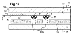
− 開口部が貫通開口部であって、面FBが面F3と接しているとき、ダイオードの前面は、好ましくは面F3から後退している;
− 開口部が貫通開口部であり、ダイオードがリバース型に取り付けられていて、面FAが面F2と接しているとき、ダイオードは、好ましくは面F2から(面FAから)後退している;及び
− ホール(開口部)がブラインド(行き止まり)であるとき、底部厚さHfと呼ばれる残余厚さは、最大で0.3mm及び/又は少なくとも0.1mm又は少なくとも0.2mmである。
Especially:
-When the opening is a through opening and the surface FB is in contact with the surface F3, the front surface of the diode preferably recedes from the surface F3;
-When the opening is a through opening, the diode is mounted in reverse and the surface FA is in contact with the surface F2, the diode is preferably retracted from the surface F2 (from the surface FA;). -When the hole (opening) is a blind (dead end), the residual thickness, called bottom thickness Hf, is at most 0.3 mm and / or at least 0.1 mm or at least 0.2 mm.
複数のダイオードの前記セットにおけるダイオード又はすべてのダイオードは、特に、(好ましくは透明な)導電性層が設けられている面F2上に存在することができ、この導電性層は、前記ダイオードと電気的に接続するための二つ又はそれ以上の区域で構成されており、前記区域は、特にミリメートル未満のサイズの幅を有する1又は複数の絶縁ストリップによって分離されている;ここで、面F2を被覆し、さらには太陽光制御及び/又は加熱層としての機能を有する導電性層、又はいわゆるダイオードキャリアである可撓性のキャリアの前面上の導電性の(局所的な)トラックを使用することができ、面FAと面F2の間の可撓性のキャリア(ダイオードキャリア)のミリメートル未満の厚さe’2は、好ましくは最大で0.2mm又は0.2mm未満である;及び/又は
複数のダイオードの前記セットにおけるダイオードは、(好ましくは透明な)導電性層が特に設けられている面F3上にリバース型で取り付けられ、この導電性層は、前記ダイオードと電気的に接続するための二つ又はそれ以上の区域で構成されており、前記区域は、特にミリメートル未満のサイズの幅を有する1又は複数の絶縁ストリップによって分離されている;ここで、面F3を被覆し、さらには太陽光制御及び/又は加熱層としての機能を有する導電性層、又はいわゆるダイオードキャリアである可撓性のキャリアの裏面上の導電性の(局所的な)トラックを使用することができ、面FBと面F3の間の可撓性のキャリア(ダイオードキャリア)のミリメートル未満の厚さe’2は、好ましくは最大で0.2mmである。
The diode in the set of a plurality of diodes or all the diodes can be present, in particular, on a surface F2 provided with a (preferably transparent) conductive layer, which is the diode and electricity. Consists of two or more zones for connecting the diodes, the compartments being separated by one or more insulating strips, particularly having a width of less than a millimeter; where the surface F2 is Use a conductive (local) track on the front of a flexible carrier that is coated and also functions as a sun control and / or heating layer, or a so-called diode carrier. The thickness e'2 of the flexible carrier (diode carrier) between the surfaces FA and F2 is preferably less than 0.2 mm or 0.2 mm at the maximum; and / or a plurality. The diodes in the set of diodes are mounted in reverse on a surface F3 specifically provided with a (preferably transparent) conductive layer, which is for electrical connection to the diode. Consisting of two or more areas, said area is particularly separated by one or more insulating strips having a width of less than a millimeter; where the surface F3 is covered and further the sun. A conductive layer having a function as a light control and / or a heating layer, or a conductive (local) track on the back surface of a flexible carrier, which is a so-called diode carrier, can be used with the surface FB. The thickness e'2 of the flexible carrier (diode carrier) between the surfaces F3, which is less than a millimeter, is preferably 0.2 mm at the maximum.
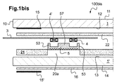
したがって、本発明は、ダイオードのために、前記積層中間層の局所的な切り取りを行うことを提案する。特に、先行技術で行われてきたように、ダイオードキャリア(PCBボード、すなわちプリント回路基板)の周囲をぐるりと取り囲んで中間層を切り取ることは、品質の低下したアセンブリを生じるリスク(気泡、層間剥離、外観上の欠陥)を増加させるため、本発明では、かかる周囲の切り取りの必要性を回避している。特に、キャリアの裏面上にPVBシートを追加しなければならないという必要性を回避するために、ダイオードキャリアは非常に薄い。共通ホール中の複数のダイオードのグループは、最大で20mmの幅又は長さの領域Sを占拠することができる。
積層中間層は、好ましくはダイオードとできるだけ近くにあり、かつ好ましくは切り取りの間のダイオードの位置の許容誤差(公差)を考慮したものであり、ここで、かかる切り取りは、好ましくは、(たとえ中間層が柔軟なものであったとしても)ダイオードの幅よりも広い幅となるように選択される。
Therefore, the present invention proposes to make a local cut of the laminated intermediate layer for the diode. In particular, cutting off the intermediate layer around a diode carrier (PCB board, or printed circuit board), as has been done in the prior art, risks resulting in poor quality assembly (bubbles, delamination). , Appearance defects), the present invention avoids the need for such perimeter cutouts. In particular, the diode carrier is very thin to avoid the need to add a PVB sheet on the back of the carrier. A group of diodes in a common hole can occupy a region S up to 20 mm wide or long.
The laminated intermediate layer is preferably as close as possible to the diode and preferably takes into account the position tolerance (tolerance) of the diode between the cuts, where such cuts are preferably (even in the middle). It is chosen to be wider than the width of the diode (even if the layer is flexible).
さらに、グレージングルーフは、平行光学系のセットを含み、それぞれの平行光学系は、好ましくは貫通した開口部中の、専用の一つの発光ダイオードと呼ばれる一つの発光ダイオードと組み合わされるか、又は好ましくは貫通した、共通開口部中の複数のダイオードのグループと組み合わされる。 In addition, the glazing roof includes a set of parallel optics, each of which is preferably combined with or preferably combined with a single light emitting diode, called a dedicated light emitting diode, in a through opening. Combined with a group of diodes in a common opening that penetrates.
(透明な材料から作製された)それぞれの平行光学系は、面F2と面F3の間に、ダイオードの前面と面F3の間の少なくとも一つの機能性部分とともに配置されている。 Each parallel optic (made of transparent material) is located between surfaces F2 and F3, along with at least one functional portion between the front surface of the diode and the surface F3.
平行光学系は照明を高めることを可能にし、かつ/又は前側又は後側の乗客間での読書領域ごとの照明をより扱いやすいものとすることを可能にする。 The parallel optics make it possible to increase the illumination and / or make the illumination per reading area between front or rear passengers more manageable.
積層中間層の好ましくは貫通した開口部は、その導入とその統合を容易にし、その性能を改善する。 A preferably penetrating opening in the laminated intermediate layer facilitates its introduction and integration and improves its performance.
全く予想外なことに、貫通開口部を採用する場合、前記平行光学系の操作に悪影響を及ぼすほどには、前記中間層は流動しない。 Quite unexpectedly, when a through opening is adopted, the intermediate layer does not flow to the extent that it adversely affects the operation of the parallel optics.
1又は複数の平行光学系は、ダイオードによって発せられる光のための出口面を有する。1又は複数の平行光学系は透明であり(光を反射しない)、ダイオードによって発せられる光を通過させる。 One or more parallel optics have an outlet surface for the light emitted by the diode. One or more parallel optics are transparent (do not reflect light) and allow the light emitted by the diode to pass through.
好ましくは:
− (前面から出る光を測定した)ダイオードの発光の半値角(半減角)は、好ましくは少なくとも50°であり;
− それぞれの平行光学系の出口における画角は、最大で40°である。
Preferably:
-The half-value angle (half-angle) of the light emission of the diode (measured by measuring the light emitted from the front) is preferably at least 50 °;
-The maximum angle of view at the exit of each parallel optical system is 40 °.
好ましくは、(テクスチャー加工されたプレート、すなわち、テクスチャープレートを有する)少なくとも一つの又はそれぞれの平行光学系は、以下を含む:
(a)出口面側の二次元のモチーフの配列であって、特に、ベース(基部)とチップ型(傾斜若しくは勾配型)又はリッジ型の頂点を含み、前記頂点は任意に先端を切り取られており、前記ベースは最大で10又は最大で5、さらには最大で2の、長さと幅のアスペクト比を有している、前記配列;又は
(b)第一のプリズムの配列及び第二のプリズムの配列を含むプリズムのアセンブリであって、
第一のプリズムの配列における、第一の配列のすべてのモチーフは、(自動車の軸に対する)ルーフの長手方向の端面に対して平行な方向に向かって長手方向に延在するか、又は(自動車の軸に対する)ルーフの長手方向の端面に対して最大で10°又は最大で5°、さらには最大で2°の角度を形成する、F3側に面したプリズムであり、かつ
第二の配列は、第一のプリズムの配列と交差しており、第二の配列のすべてのモチーフが、第一のプリズムの配列の長手方向の軸に対して垂直な方向に向かって長手方向に延在するか、又は第一のプリズムの配列の長手方向の軸に対して最大で90±10°又は90±2°の角度を形成する、F3側に面したプリズムである、前記アセンブリ。
Preferably, at least one or each parallel optic (having a textured plate, i.e. a textured plate) includes:
(A) An array of two-dimensional motifs on the exit surface side, including a base (base) and a tip-type (inclined or gradient-type) or ridge-shaped apex, and the apex is arbitrarily cut off. The base has a length and width aspect ratio of up to 10 or up to 5, and even up to 2, said array; or (b) an array of first prisms and a second prism. An assembly of vertices containing an array of
In the arrangement of the first prism, all the motifs of the first arrangement extend longitudinally in the direction parallel to the longitudinal end face of the roof (relative to the axis of the car) or (car). A prism facing the F3 side, forming an angle of up to 10 ° or up to 5 ° and even up to 2 ° with respect to the longitudinal end face of the roof (with respect to the axis of), and the second arrangement is Is it intersecting with the first prism array and all the motifs in the second array extend longitudinally in the direction perpendicular to the longitudinal axis of the first prism array? , Or a prism facing the F3 side, forming an angle of up to 90 ± 10 ° or 90 ± 2 ° with respect to the longitudinal axis of the arrangement of the first prism, said assembly.
好ましくは、(a)による少なくとも一つの又はそれぞれの平行光学系は、その厚みをもって部分的にテクスチャー加工されたテクスチャープレートと呼ばれる平面の機能性プレートを含み、このプレートは、好ましくは貫通した開口部中のダイオードに面した、又は好ましくは貫通した、共通開口部中の複数のダイオードのグループに面した、面F2の方向を向いている入口面と、面F3の方向を向いている出口面とを有し、前記テクスチャーがミリメートル未満の高さ(好ましくはEAよりも小さい高さ)のモチーフを形成する。 Preferably, at least one or each parallel optic according to (a) comprises a planar functional plate called a texture plate that is partially textured with its thickness, which plate preferably has a penetrating opening. An inlet surface facing the inner diode, or preferably penetrating, facing a group of diodes in a common opening, facing the plane F2 and an exit plane facing the plane F3. the have the texture submillimeter height (preferably less height than E a) forming a motif.
好ましくは、(b)による少なくとも一つの又はそれぞれの平行光学系は、以下:
− その厚みをもって部分的にテクスチャー加工された第一のテクスチャープレートと呼ばれる第一の平面の機能性プレートであって、このプレートは、好ましくは貫通した開口部中のダイオードに面した、又は好ましくは貫通した、共通開口部中の複数のダイオードのグループに面した、面F2の方向を向いている入口面と、面F3の方向を向いているテクスチャー加工された出口面とを有し、前記テクスチャーがミリメートル未満の高さ(好ましくはEAよりも小さい高さ)の(第一のプリズムの配列の)前記モチーフを形成する、第一の平面の機能性プレート;及び
− その厚みをもって部分的にテクスチャー加工された第二のテクスチャープレートと呼ばれる第二の平面の機能性プレートであって、このプレートは、好ましくは貫通した開口部中のダイオードに面した、又は好ましくは貫通した、共通開口部中の複数のダイオードのグループに面した、面F2の方向の第一のプレートの出口の方向を向いている入口面と、面F3の方向を向いているテクスチャー加工された出口面とを有し、前記テクスチャーがミリメートル未満の高さ(好ましくはEAよりも小さい高さ)の(第二のプリズムの配列の)前記モチーフを形成する、第二の平面の機能性プレート;
を含む。
Preferably, at least one or each parallel optical system according to (b) is:
-A first planar functional plate called the first texture plate that is partially textured to that thickness, which preferably faces or preferably faces the diode in the through opening. It has an inlet surface facing the direction of surface F2 and a textured exit surface facing the direction of surface F3, facing a group of a plurality of diodes in a common opening that penetrates the texture. There submillimeter height (preferably less height than E a) (the sequence of the first prism) forming the motifs, functional plates of the first plane; and - partially with the thickness A second planar functional plate called a textured second texture plate, which is preferably in a common opening facing or preferably penetrating a diode in a penetrating opening. It has an inlet surface facing the exit of the first plate in the direction of surface F2 and a textured exit surface facing the direction of surface F3, facing a group of diodes. A functional plate in a second plane that forms the motif (in an array of second prisms) whose texture is less than a millimeter high (preferably less than EA);
including.
(第一の、さらには第二の)テクスチャープレート(テクスチャー加工されたプレート)は、好ましくは貫通した開口部中の(有用な区域にある)ダイオードの又は好ましくは貫通した、共通開口部中の複数のダイオードのグループのダイオードの前面の幅よりも大きい幅であるか又はそれと等しい幅を有する。 The (first and second) textured plate (textured plate) is preferably in a diode (in a useful area) in a through opening or preferably in a through, common opening. It has a width greater than or equal to the width of the front surface of the diodes in a group of diodes.
(第一のプレートの)入口面は、好ましくは貫通した開口部中のダイオード又は好ましくは貫通した、共通開口部中の複数のダイオードのグループのダイオードの前面から、好ましくは離れている。 The inlet surface (of the first plate) is preferably away from the front of the diode in the opening, preferably through, or the diode in the group of diodes, preferably in the common opening, which penetrates.
好ましくは、ダイオード/入口及び出口の空隙/第一及び第二のテクスチャープレートの高さはまとめて、最大で1mmさらには0.9mmである。 Preferably, the height of the diode / inlet and outlet voids / first and second texture plates together is a maximum of 1 mm and even 0.9 mm.
(第一の及びさらには第二の)テクスチャー加工された平面のプレートは、有利には、湾曲した又は平面の表面から形成された複数の幾何学的モチーフを含む。好ましくは、繰り返しの幾何学的モチーフ、すなわち、実質的に同じ形状を有し、互いに実質的に等しい間隔で配置された幾何学的モチーフを使用することができる。 Textured flat plates (first and even second) preferably contain multiple geometric motifs formed from curved or flat surfaces. Preferably, it is possible to use repetitive geometric motifs, i.e. geometric motifs that have substantially the same shape and are spaced substantially equal to each other.
もちろん、(第一の及びさらには第二の)テクスチャー加工された平面のプレートによって被覆される区域の形状は、モチーフの形状とは独立している。
(第一の及びさらには第二の)テクスチャープレートの高さは、5μm〜1mmの間に含まれる高さであり、好ましくは10μm〜500μmの間に、特に20μm〜300μmの間にあり、好ましくは少なくとも50μmであって、最大で200μmである。
Of course, the shape of the area covered by the (first and even second) textured flat plates is independent of the shape of the motif.
The height of the (first and even second) texture plate is a height contained between 5 μm and 1 mm, preferably between 10 μm and 500 μm, particularly between 20 μm and 300 μm, and is preferred. Is at least 50 μm and at most 200 μm.
(第一の及びさらには第二の)テクスチャープレートは、散乱を防止するために低い粗さを有するものでなければならない。粗さとは別に、モチーフの最も高い点と最も低い点の間の距離に等しい、テクスチャーの深さ又は高さを定義することも可能である。
モチーフの寸法は、約10μm〜500μmであり、さらに好ましくは100μm〜300μmであり、好ましくは少なくとも50μmのサイズである。
The (first and even second) texture plates must have low roughness to prevent scattering. Apart from the roughness, it is also possible to define the depth or height of the texture, which is equal to the distance between the highest and lowest points of the motif.
The size of the motif is about 10 μm to 500 μm, more preferably 100 μm to 300 μm, and preferably at least 50 μm in size.
(第一の及びさらには第二の)テクスチャープレートは、その厚みをもって部分的にテクスチャー加工されており、言い換えれば、平滑な面と、テクスチャー加工された面の平滑な面に最も近い点との距離は一定の厚さを有する。好ましくは、プレートの(一定の)残余厚さは、テクスチャー加工された面(プリズムの配列であれば、出口面)間の最も低い点と、その反対側の面(プリズムの配列であれば、入口面)との間の距離として定義される。残余厚さは少なくとも50μmであり、さらには最大で200μmである。 The (first and even second) textured plates are partially textured with their thickness, in other words, the smooth surface and the point closest to the smooth surface of the textured surface. The distance has a certain thickness. Preferably, the (constant) residual thickness of the plate is the lowest point between the textured surfaces (outlet surfaces if in an array of prisms) and the opposite surface (if an array of prisms). It is defined as the distance to the entrance surface). The residual thickness is at least 50 μm and further up to 200 μm.
(第一の及びさらには第二の)テクスチャープレート(又はそれが有する部分)は、ポリウレタン又はポリカーボネート(PC)又はポリメチルメタクリレート(PMMA)などの熱可塑性ポリマーから作製することができる。PMMA又はPCから作製された成形部分を使用することもできる。テクスチャーは、圧延(すなわちキャスティング)、熱成形、エッチング等で製造することができ、特にポリマー材料ではレーザーエッチングにより製造することができる。所望のテクスチャーの形状によって、その製造過程では、必ずしも完全な幾何学的形状:丸みを帯びたリッジや頂点にまで導く必要はない。 The (first and even second) texture plate (or portion it has) can be made from a thermoplastic polymer such as polyurethane or polycarbonate (PC) or polymethylmethacrylate (PMMA). Molded parts made from PMMA or PC can also be used. The texture can be produced by rolling (ie casting), thermoforming, etching or the like, and in particular for polymer materials it can be produced by laser etching. Depending on the shape of the desired texture, the manufacturing process does not necessarily have to lead to a perfect geometry: rounded ridges or vertices.
好ましくは、モチーフは互いにできるだけ近いものであり、例えばそのベース(基部)が1mm未満しか離れておらず、好ましくは0.5mm未満しか離れていないものである。 Preferably, the motifs are as close as possible to each other, eg, their bases are less than 1 mm apart, preferably less than 0.5 mm apart.
より好ましくは、モチーフは連続しているか又は実質的に連続している。モチーフが、その表面の少なくとも一つの部分で互いに接しているとき、そのモチーフは連続しているということができる。モチーフが連続していれば(第一の及びさらには第二の)プレートの表面がよりテクスチャー加工されることになるため、モチーフは連続していることが好ましい。ある種のモチーフでは、モチーフ間が完全に連続するものでなくともよい。これは、特に、ベース(基部)が円形であって接触しているときに、円形間にモチーフに属しない領域があるような場合である。完全な連続性とは、モチーフのベース(基部)の輪郭が全体として、隣接するモチーフの輪郭の一部を形成することを意味する。 More preferably, the motifs are continuous or substantially continuous. When the motifs touch each other on at least one part of their surface, the motifs can be said to be continuous. It is preferable that the motifs are continuous, because the surface of the plate (first and even second) will be more textured if the motifs are continuous. For some motifs, the motifs do not have to be completely continuous. This is especially the case when the bases are circular and in contact, there are areas between the circles that do not belong to the motif. Perfect continuity means that the contour of the base of the motif as a whole forms part of the contour of the adjacent motif.
ある種のモチーフは完全に連続していてもよく、したがって、プレートの表面の全体が少なくとも一つのモチーフを形成する。モザイク加工とすることもできる。特に、正方形又は長方形又は六角形をベースとするモチーフは、そのベースが同一であれば完全に連続することができる。正方形又は長方形のベースの場合は、モチーフが完全に連続するのであれば、前記ベースは整列することになる。六角形のベースの場合は、それらのベースがハニカム(ハチの巣)を形成することが望ましい。 Certain motifs may be completely continuous, so the entire surface of the plate forms at least one motif. It can also be mosaic processed. In particular, motifs based on squares or rectangles or hexagons can be completely continuous if their bases are the same. In the case of a square or rectangular base, the bases will be aligned if the motifs are perfectly continuous. In the case of hexagonal bases, it is desirable that those bases form a honeycomb (honeycomb).
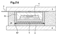
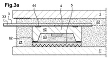
有利には、少なくとも一つの又はそれぞれの平行光学系は、好ましくは貫通した開口部中の、好ましくは一体化された(モノリシックの)一つの部分であるか((a)のために)又は結合した複数の部品(例えば2つの部品、特に2つのテクスチャープレート)から作られている部分であって、任意に共通する、好ましくは貫通した開口部中のダイオードキャリア上に取り付けられた又はダイオード又は複数のダイオードのグループ上に取り付けられた部分であり、当該部分は、以下を含む:
− 平行光学系の機能性部分、特に、(第一の)テクスチャープレート及び任意の第二のテクスチャープレート((b)のために);及び
− ダイオード又は複数のダイオードのグループのうちの少なくとも一つのダイオードの(パッケージの)端面に沿った面F2の方向に、特に(第一の)テクスチャープレートの方向にある、周辺拡張部(周縁、リム)であり、特にその幅Wが、最大で1.5mm、少なくとも0.1mm、さらに好ましくは少なくとも0.5mmであって、前記端面と接しているか、さらに好ましくは最大で2mmだけ離れており、又は(好ましくは貫通した開口部を形成する壁で)積層中間層に接している。
Advantageously, at least one or each parallel optic is preferably a united (monolithic) part of the opening, preferably integrated (because of (a)) or coupled. A part made of a plurality of parts (eg, two parts, particularly two texture plates), optionally common, preferably mounted on a diode carrier in a through opening, or a diode or a plurality. A part mounted on a group of diodes, which includes:
-Functional parts of the parallel optics, in particular the (first) texture plate and any second texture plate (for (b)); and-the diode or at least one of a group of diodes. Peripheral extensions (peripheries, rims) in the direction of surface F2 along the (package) end face of the diode, especially in the direction of the (first) texture plate, with a maximum width W of 1. 5 mm, at least 0.1 mm, more preferably at least 0.5 mm, in contact with the end face, more preferably separated by up to 2 mm, or (preferably at a wall forming a penetrating opening). It is in contact with the laminated intermediate layer.
機能性のテクスチャー加工された区域の他の、周辺拡張部は、テクスチャー加工された面であっても平滑な面であってもよい。
周辺拡張部は、面F3に面した面であって、テクスチャー加工された出口面から突出する面を有することができる(例えば許容される厚さの、出口の空隙を残しておくため)。
Other peripheral extensions of the functional textured area may be textured or smooth surfaces.
The peripheral extension can have a surface facing surface F3 that protrudes from the textured exit surface (eg, to leave an outlet void of acceptable thickness).
周辺拡張部は、面F3に面した面であって、テクスチャー加工された出口面の最も高い位置にある面を有することができる。テクスチャー加工された出口面及び/又は周辺拡張部は、面F3と接しているか、又は特にモチーフが高さをもって立ち上がっているものであれば、好ましくは面F3から後退(セットバック)している。
周辺拡張部、及び/又は(第一の)テクスチャープレート及び第二のテクスチャープレートは、任意に共通する、好ましくは貫通した開口部中に全体として収容されうる。周辺拡張部及び/又はテクスチャープレートは、面FBから突出しない。
The peripheral extension can have a surface facing the surface F3, which is at the highest position of the textured exit surface. The textured exit surface and / or peripheral extension is preferably set back from the surface F3 if it is in contact with the surface F3 or, in particular, if the motif rises at a height.
The peripheral extension and / or the (first) texture plate and the second texture plate can be accommodated as a whole in any common, preferably penetrating opening. The peripheral extension and / or the texture plate does not protrude from the surface FB.
周辺拡張部は、(L字型の断面部分の)少なくとも一つの取り付け足部の形態をとることができ、好ましくは、以下のような、(U字型の断面部分の)少なくとも二つの取り付け足部の形態をとることができる:
− ダイオードへの平行光学系の取り付けのためのもの、前記1又は複数の取り付け足部は、ダイオードの端面のいずれかの側にあって、ダイオードの端面から離れているか、又はダイオードキャリア上にあり、圧入することによって、又は好ましくはダイオード又は複数のダイオードのグループの前面を越えて接着接合することによって、ダイオードに平行光学系を取り付ける(入口の空隙を確保するため);
− それぞれのダイオード又は複数のダイオードのグループへの平行光学系の取り付けのためのもの、前記1又は複数の取り付け足部は、ダイオードの端面のいずれかの側にあって、ダイオードの端面から離れているか、又はダイオードキャリアと接しており、圧入することによって、又は好ましくはダイオード又は複数のダイオードのグループの前面を越えて接着接合することによって、それぞれのダイオード又は複数のダイオードのグループに平行光学系を取り付ける(入口の空隙を確保するため);
− ダイオードキャリアへの平行光学系の取り付けのためのもの。
The peripheral extension can take the form of at least one attachment foot (of the L-shaped cross section), preferably at least two attachment feet (of the U-shaped cross section), such as: Can take the form of a part:
-For mounting parallel optics to a diode, said one or more mounting feet are on either side of the diode end face, away from the diode end face, or on the diode carrier. Attach the parallel optics to the diode by press-fitting, or preferably by bonding over the front of the diode or group of diodes (to ensure clearance at the inlet);
-For mounting parallel optics to each diode or group of diodes, said one or more mounting feet on either side of the diode end face, away from the diode end face. Parallel optics to each diode or group of diodes, either by contacting with a diode carrier and by press fitting, or preferably by adhesive bonding over the front of the diode or group of diodes. Install (to secure a gap at the entrance);
-For mounting parallel optics on diode carriers.
周辺拡張部は、好ましくは、好ましくは貫通した、開口部中のダイオード又は共通する、好ましくは貫通した、開口部中の複数のダイオードのグループの周囲部分を形成する。この部分はU字型の断面を有する。 The peripheral extension preferably forms a perimeter portion of a group of diodes in the opening, preferably penetrating, or a common, preferably penetrating, group of diodes in the opening. This portion has a U-shaped cross section.
好ましくは、この周囲部分は、ダイオード又は複数のダイオードのグループを収容する筐体を含み、特にこの周囲部分の壁は、ダイオード又は複数のダイオードのグループを保持するためのスタブを含み、このスタブは、好ましくは規則的に分配されており、好ましくはその数は少なくとも2つである。
この周囲の拡張部の高さは、好ましくは面FBから最大で0.3mmの距離であり、好ましくは面FBから最大で0.1mm離れている。
Preferably, the perimeter comprises a diode or a housing containing a group of diodes, in particular the wall of the perimeter comprises a stub for holding the diode or a group of diodes, the stub. , Preferably regularly distributed, preferably at least two in number.
The height of the peripheral extension portion is preferably a maximum distance of 0.3 mm from the surface FB, and preferably a maximum distance of 0.1 mm from the surface FB.
ダイオード上に取り付ける又はダイオードキャリア上に取り付けることについて、一つの代替の実施形態では、(a)による平行光学系は、面F3と1又は複数の好ましくは貫通した開口部を有する積層中間層の間のテクスチャー加工された透明なフィルムとすることができる。このとき、((a)による)平行光学系は、すべてのダイオードにとって共通するものとなる。
複数のダイオードのセットを有する区域を被覆するそれぞれのテクスチャー加工された透明なフィルムの領域をテクスチャー加工することができ、したがって、それぞれのテクスチャー加工された透明なフィルムは、一つのダイオード又は複数のダイオードのグループのそれぞれに面した、1又は複数のテクスチャー加工された領域を含むことができ、そこに隣接する領域は平滑である(透明性を維持するため)。
For mounting on a diode or mounting on a diode carrier, in one alternative embodiment, the parallel optics according to (a) are between surface F3 and one or more laminated intermediate layers with one or more preferably through openings. It can be a transparent film with a textured finish. At this time, the parallel optical system (according to (a)) becomes common to all diodes.
Areas of each textured transparent film covering an area with multiple sets of diodes can be textured, thus each textured transparent film is a diode or multiple diodes. Can include one or more textured areas facing each of the groups of, and adjacent areas thereof are smooth (to maintain transparency).
テクスチャー加工された透明なフィルムは、プラスチック(有機ポリマー)から作製されたフィルムであってよく、好ましくはポリエチレンテレフタレート(PET)、ポリカーボネート、ポリメチルメタクリレート又はポリスチレンである。 The textured transparent film may be a film made from a plastic (organic polymer), preferably polyethylene terephthalate (PET), polycarbonate, polymethylmethacrylate or polystyrene.
(b)による平行光学系は、面F3と1又は複数の好ましくは貫通した開口部を有する積層中間層の間の、第一のテクスチャー加工された透明なフィルム及び第二の(交差する)テクスチャー加工された透明なフィルムとすることができる。このとき、平行光学系は、すべてのダイオードにとって共通するものとなる。複数のダイオードのセットを有する区域を被覆するテクスチャー加工された透明なフィルムの領域をテクスチャー加工することができ、したがって、テクスチャー加工された透明なフィルムは、一つのダイオード又は複数のダイオードのグループのそれぞれに面した、1又は複数のテクスチャー加工された領域を含むことができ、そこに隣接する領域は平滑である(透明性を維持するため)。 The parallel optics according to (b) are a first textured transparent film and a second (intersecting) texture between surface F3 and a laminated intermediate layer with one or more preferably through openings. It can be a processed transparent film. At this time, the parallel optical system becomes common to all diodes. Areas of the textured transparent film covering an area with a set of diodes can be textured, thus the textured transparent film is a diode or a group of diodes, respectively. It can include one or more textured areas facing, the areas adjacent to it are smooth (to maintain transparency).
しかしながら、好ましくは貫通した開口部中に取り付けられた平行光学系のセットを使用することも好ましい。 However, it is also preferable to use a set of parallel optics mounted in the through openings.
好ましくは:
− ((a)又は(b)の)平行光学系を有するダイオードは、PVBシートにおけるブラインドの若しくは(好ましくは)貫通した開口部にあるか、又はPVBシート/任意の機能性被覆を有する機能性フィルム/PVBシートにおけるブラインドの若しくは(好ましくは)貫通した開口部にあり;又は
− ブラインドの若しくは(好ましくは)貫通した開口部は、複数のダイオードのグループにおける前記複数のダイオードに共通しており、平行光学系((a)又は(b)、特に第一のテクスチャープレート若しくはフィルム)の部分は、ダイオード間のスペーサーを形成するか、又はダイオード間のスペーサーは、平行光学系((a)又は(b)、特に第一のテクスチャープレート若しくはフィルム)から分離した部分である。
Preferably:
-The diode having the parallel optics ((a) or (b)) is in the blind or (preferably) through opening in the PVB sheet, or the PVB sheet / functionality with any functional coating. The blind or (preferably) penetrating opening in the film / PVB sheet is in the blind or (preferably) penetrating opening; or-the blind or (preferably) penetrating opening is common to the plurality of diodes in the group of diodes. The part of the parallel optics ((a) or (b), especially the first texture plate or film) forms a spacer between the diodes, or the spacer between the diodes is a parallel optic ((a) or (a) or ( b), especially the portion separated from the first texture plate or film).
複数のダイオードのグループにおける前記複数のダイオードは、例えば最大で0.5mmだけ離れているか、又はそのインターダイオードスペースは、透明なスペーサーを含む。
(任意のパッケージによって画定される)ダイオードの幅(例えば直径又は長さ(最大寸法))は、最大で15mm、さらには最大で10mmである。
The plurality of diodes in a group of plurality of diodes are separated by, for example, up to 0.5 mm, or their interdiode space comprises a transparent spacer.
The width of the diode (defined by any package) (eg, diameter or length (maximum dimension)) can be up to 15 mm and even up to 10 mm.
モチーフのベース(基部)は、好ましくは発光面に平行である。 The base of the motif is preferably parallel to the light emitting surface.
モチーフの先端が平面で切断された部分の高さは、テクスチャーのピッチ(一周期)の値の最大で10%である。
モチーフ(第一のプレート及び/又はテクスチャー加工された第二のプレート)は、以下のものでありうる:
− 凸形状、すなわち、プレートのテクスチャー加工された面の一般面に対して外側に延びる形状;又は
− 凹形状、すなわち、プレートのバルク(かさ)内に埋め込まれた形状。
The height of the portion where the tip of the motif is cut in a plane is a maximum of 10% of the value of the pitch (one cycle) of the texture.
The motif (first plate and / or textured second plate) can be:
-Convex, that is, a shape that extends outward with respect to the general surface of the textured surface of the plate; or-Concave, that is, a shape that is embedded within the bulk of the plate.
二次元のモチーフは、好ましくは、頂点でのゼロでない半角値を有する、軸対称(線対称)のピラミッド形又は円錐形のものであり、この二次元のモチーフ又はプリズムは、35°〜55°の範囲又は40°〜50°の範囲の、さらに好ましくは45°の、頂点での半角値を有する。 The two-dimensional motif is preferably an axisymmetric pyramidal or conical with a non-zero half-width value at the apex, and the two-dimensional motif or prism is 35 ° to 55 °. It has a half-width value in the range of 40 ° to 50 °, more preferably 45 °, at the apex.
二次元のモチーフのベース(基部)は、例えば、多角形、正方形、長方形、六角形又は三角形、さらには丸みを帯びたもの、すなわち円、などである。
モチーフのベースを含むことができる最も小さい円は、モチーフの高さの最大で2倍の直径を有する円に内接するものである。
The base of a two-dimensional motif is, for example, a polygon, a square, a rectangle, a hexagon or a triangle, and even a rounded one, ie, a circle.
The smallest circle that can contain the base of the motif is inscribed in a circle that has a diameter of up to twice the height of the motif.
モチーフは、以下のものでありうる:
− 高さをもって立ち上がっているもの、したがって、中実なもの;又は
− へこんでいる(埋め込まれている)もの(言い換えれば、逆さになっているもの)、空洞の壁が1又は複数の表面を形成し、その表面の頂点(先端部分)が面F2の方向を向いており、その空洞の上面(頂面)が、モチーフのベース(基部)の輪郭を画定するもの。
The motif can be:
-Rising at height, and thus solid; or-Depressed (embedded) (in other words, upside down), hollow walls on one or more surfaces Formed, the apex (tip portion) of the surface faces the direction of the surface F2, and the upper surface (top surface) of the cavity defines the outline of the base (base) of the motif.
さらに、二次元のモチーフは、以下のものでありうる:
− 高さをもって立ち上がっているもの、したがって、中実なもの、例えば円錐形の表面を有するもの、特に頂上部で隔てられた側面を有するもの;又は
− へこんでいる(埋め込まれている)もの(言い換えれば、逆さになっているもの)、空洞の壁が1又は複数の円錐状の表面を形成し、その表面の頂点が面F2の方向を向いており、その空洞の上面(頂面)がモチーフのベース(基部)の輪郭を画定するもの。
In addition, the two-dimensional motif can be:
-Rising at height, and thus solid, such as those with a conical surface, especially those with sides separated by the apex; or-Depressed (embedded) ( In other words, it is upside down), the walls of the cavity form one or more conical surfaces, the vertices of the surface point in the direction of surface F2, and the top surface (top surface) of the cavity. The one that defines the outline of the base of the motif.
好ましくは二次元のモチーフは、ピラミッドの平面である(側面の)面を有する。一般的な円錐形は平面的な表面を有していない。二次元のモチーフは、円錐形やピラミッド形場合のように、例えば結果的にはチップ(傾斜又は勾配)になり、すなわち、プレートの一般面から最も遠いモチーフの点がチップ(傾斜又は勾配)の頂点になる。二次元のモチーフが正角錘である場合、(プレートのテクスチャー加工された面の一般面に含まれる)ベースは正三角形である。 Preferably the two-dimensional motif has a (side) plane that is the plane of the pyramid. A typical cone does not have a flat surface. The two-dimensional motif results in a tip (tilt or slope), for example, as in the case of a cone or pyramid, that is, the point of the motif farthest from the general plane of the plate is the tip (tilt or slope). Become the top. If the two-dimensional motif is a conformal weight, the base (included in the general surface of the textured surface of the plate) is an equilateral triangle.
ダイオードは、チップオンボード型のダイオードとすることもでき、最も好ましくは、周辺パッケージを含む、表面実装型デバイス(SMD)である。 The diode can also be a chip-on-board diode, most preferably a surface mount device (SMD) that includes peripheral packages.
一つの好ましい実施態様では、それぞれのダイオード、好ましくは、それぞれの電力ダイオードは、少なくとも一つの半導体チップを含む電子部品であり、その電子部品の端面を封入した(及びダイオードの端面を規定する)、特にポリマー又はセラミックの周辺パッケージを備えており、当該パッケージは(半導体チップから突出して)半導体チップを取り囲んでいる。 In one preferred embodiment, each diode, preferably each power diode, is an electronic component that includes at least one semiconductor chip and encloses the end faces of the electronic components (and defines the end faces of the diodes). In particular, it comprises a polymer or ceramic peripheral package, which surrounds the semiconductor chip (protruding from the semiconductor chip).
パッケージは、ダイオードの最大厚さ(高さ)e2に相当するものとすることができる。パッケージは、例えばエポキシから作製されている。ポリマーパッケージは、積層の間に任意に圧縮される(積層後の最終的な厚さは初期の厚さよりも小さくすることができる)。(ポリマーの)パッケージは、不透明であってもよい。 The package can correspond to the maximum thickness (height) e2 of the diode. The package is made from, for example, epoxy. The polymer package is optionally compressed during lamination (the final thickness after lamination can be less than the initial thickness). The (polymeric) package may be opaque.
パッケージ(一体型又は2つの部分から作製されているパッケージ)は、チップを有する支持体を形成する部分及びチップよりも上側で支持体から離れて広がるリフレクターを形成する部分を含み、保護樹脂及び/又は色変換機能を有する材料を含む。パッケージの前面はチップを覆っているこの材料の表面として定義され、この表面は、リフレクターの「前」面よりも後退しているか又は同じ高さである。 The package (integral or package made of two parts) includes a portion forming a support having a chip and a portion forming a reflector above the chip and extending away from the support, a protective resin and /. Alternatively, a material having a color conversion function is included. The front surface of the package is defined as the surface of this material covering the chip, which surface is receding or flush with the "front" surface of the reflector.
好ましくは、1又は複数のダイオードは、ダイオードキャリアの前面に取り付けられた表面実装型デバイスであり、1又は複数のダイオードは、ランバート又は準ランバート放射パターンを有する。 Preferably, the one or more diodes are surface mount devices mounted in front of the diode carrier and the one or more diodes have a Lambertian or quasi-Lambertian emission pattern.
一つの好ましい実施態様では、面FAと面FBの間の、好ましくはPVBから作製されている積層中間層の厚さは、0.7〜0.9mmの範囲(単一のシート又は第一と第二のシート)であって、ダイオードは、ダイオードキャリアの前面に取り付けられた表面実装型デバイスであり、ダイオードキャリアの厚さe’2は、最大で0.2mmであり、より好ましくは最大で0.15mm、さらには最大で0.05mmである。 In one preferred embodiment, the thickness of the laminated intermediate layer between the surface FA and the surface FB, preferably made from PVB, ranges from 0.7 to 0.9 mm (single sheet or first). Second sheet), the diode is a surface mount device mounted on the front surface of the diode carrier, the diode carrier thickness e'2 is up to 0.2 mm, more preferably up to. It is 0.15 mm, and even 0.05 mm at the maximum.
プリント回路基板(PCB)であってよいダイオードキャリアの幅は、好ましくは最大で5cmであり、より好ましくは最大で2cm、さらには最大で1cmである。一般的に正方形の形状であるダイオードのように、単一の半導体チップを有するダイオードの幅(又は長さ)は、好ましくは最大で5mmである。一般的に長方形の形状であるダイオードのように、複数の半導体チップを有するダイオード(典型的にはパッケージで囲まれている)の長さは、好ましくは最大で20mm、より好ましくは最大で10mmである。 The width of the diode carrier, which may be a printed circuit board (PCB), is preferably up to 5 cm, more preferably up to 2 cm, and even up to 1 cm. The width (or length) of a diode having a single semiconductor chip, such as a diode that is generally square in shape, is preferably up to 5 mm. A diode having multiple semiconductor chips (typically enclosed in a package), such as a diode that is generally rectangular in shape, has a length of preferably up to 20 mm, more preferably up to 10 mm. is there.
特に、貫通開口部を有する単一のシートの場合には、−特に任意に音響性の着色した又は澄明なPVBシートの場合には−、ダイオードキャリア(湾曲した積層グレージングの形状に適合するために十分に柔軟であるダイオードキャリア)は、面F2に対して又はリバース実装型構造においては面F3に対して、接着接合するかプレスする(押し付ける)ことができ、ダイオードキャリアの厚さe’2は、最大で0.15mm、さらには最大で0.1mmであって、特に、接着接合は、厚さe3の接着剤(グルー又は好ましくは両面接着剤)を使用して行うことができ、ここでe3≦0.1mm、好ましくはe3≦0.05mmであり、さらにはe3+e’2は、最大で0.15mmであり、より好ましくは最大で0.1mmである。 Especially in the case of a single sheet with through openings-especially in the case of optionally acoustically colored or clear PVB sheets-to accommodate diode carriers (curved laminated glazing shapes). A diode carrier that is sufficiently flexible) can be adhesively bonded or pressed (pressed) against the surface F2 or, in a reverse-mounted structure, against the surface F3, and the diode carrier thickness e'2 Adhesive bonding can be carried out using an adhesive of thickness e3 (glue or preferably a double-sided adhesive), with a maximum of 0.15 mm and even a maximum of 0.1 mm. e3 ≦ 0.1 mm, preferably e3 ≦ 0.05 mm, and further, e3 + e'2 is 0.15 mm at the maximum, and more preferably 0.1 mm at the maximum.
この接着剤を含めると、好ましくは、e3+et2≦e1である(ダイオードの区域におけるプリント回路基板の裏面上に上記のものがすべて存在する場合;ここで、et2はダイオードキャリアとダイオードのアセンブリの全体の厚さを意味する)。 Including this adhesive is preferably e3 + et2≤e1 (if all of the above are present on the back surface of the printed circuit board in the diode area; where et2 is the entire diode carrier and diode assembly. Means thickness).
ダイオードが存在する区域内及び/又はダイオードが存在する区域外において、キャリアの長さ全体にわたって又は個々の点で、ダイオードキャリアは接着接合することができる。周辺の接着剤は水を通さないシールを形成することができる。 Within the area where the diode is present and / or outside the area where the diode is present, the diode carrier can be adhesively bonded over the entire length of the carrier or at individual points. The surrounding adhesive can form a water-impermeable seal.
ダイオードキャリアは、局所的に配置されてもよく、より目立たないようにするために貫通開口部を任意に含む。 The diode carrier may be locally arranged and optionally includes a through opening to make it less noticeable.
ルーフは、熱可塑性材料から作製されたシート、特に積層中間層を、ダイオードキャリアの裏面と、面F2との間に又はリバース実装型構造においては面F3との間に、有することができる。 The roof can have a sheet made of a thermoplastic material, especially a laminated intermediate layer, between the back surface of the diode carrier and the surface F2 or, in a reverse mount structure, the surface F3.
1又は複数のフィルムから形成される積層中間層、すなわち、面FA及び面FBの間の、及び/又は裏面上のシート及び/又は面FBと面F3との間のシートから形成される積層中間層は、ポリビニルブチラール(PVB)、ポリウレタン(PU)又はエチレン−酢酸ビニルコポリマー(EVA)から作製されていてよく、例えば、0.2〜1.1mmの厚さを有する。
Solutia社又はEastman社からのRC41のような、従来から使用されているPVBを選択することが可能である。
Laminated intermediates formed from one or more films, i.e., sheets between face FA and face FB and / or sheets on the back surface and / or sheets between face FB and face F3. The layer may be made of polyvinyl butyral (PVB), polyurethane (PU) or ethylene-vinyl acetate copolymer (EVA) and has a thickness of, for example, 0.2-1.1 mm.
Conventionally used PVBs, such as RC41 from Solutia or Eastman, can be selected.
したがって、面FA及び面FBの間の及び/又は裏面上のシート及び/又は面FBと面F3との間のシートから形成される積層中間層は、振動音響減衰特性を有する粘弾性プラスチックから作製され、特にポリビニルブチラール(PVB)と可塑剤に基づく、少なくとも一つのいわば「中央」層を含むことができ、この積層中間層は、さらに標準的なPVBから作製された2つの外側層を含み、中央層はこの2つの外側層の間にある。音響性シートの例に言及するものとして、欧州特許第0 844 075号明細書を挙げることができる。音響性PVBに言及するものとして、国際公開第2012/025685号、国際公開第2013/175101号、特に着色されたPVBについて、国際公開第2015/079159号の特許出願を挙げることができる。 Therefore, the laminated intermediate layer formed from the sheet between the surface FA and the surface FB and / or the sheet on the back surface and / or the sheet between the surface FB and the surface F3 is made of a viscoelastic plastic having a vibration-acoustic damping property. And can include at least one so-called "central" layer, especially based on polyvinyl butyral (PVB) and plasticizer, which laminated intermediate layer further comprises two outer layers made from standard PVB. The central layer lies between the two outer layers. As an example of an acoustic sheet, European Patent No. 0844 075 can be mentioned. References to acoustic PVB include the patent applications of International Publication No. 2012/025685, International Publication No. 2013/175101, and especially for colored PVB, International Publication No. 2015/079159.
好ましくは、ルーフは、少なくとも一つの以下の特徴を有する:
− (個々の又は共通する)好ましくは貫通した開口部が、PVB(又は1又は複数のPVBシート、その界面は特に認識できる)の厚み中にある;
− (個々の又は共通する)好ましくは貫通した開口部が、特に三層又は四層の音響性積層中間層中にある;
− (個々の又は共通する)好ましくは貫通した開口部が、(特にダイオードキャリアをわずかにマスキングしている)着色した積層中間層中にある;
− (個々の又は共通する)開口部が、複合(多層シート)材料中にある[複合材料:PVBシート/透明なプラスチックフィルム、若しくはPVBシート/透明なプラスチックフィルム/PVBシートであり、前記プラスチックフィルムは、ミリメートル未満のサイズの厚さの特にPETフィルムであり、最大で0.2mm又は最大で0.1mmの厚さを有し、機能性被覆(低放射率又は太陽光制御機能及び/又は加熱機能を付与する被覆)を有する];
− (個々の)貫通開口部間の間隔が、少なくとも0.1mm又は好ましくは少なくとも0.2mmであり、読書灯の機能のためには、好ましくは最大で50cmである;
− (個々の)別個の貫通開口部にあるダイオード間の間隔が、少なくとも0.1mm又は好ましくは少なくとも0.2mmである;及び
− 貫通した又は共通する、開口部中のダイオード間の間隔が、少なくとも0.1mm又は好ましくは少なくとも0.2mmであって、さらには最大で1mmである。
Preferably, the roof has at least one of the following characteristics:
-Preferably through openings (individual or common) are in the thickness of PVB (or one or more PVB sheets, the interface thereof is particularly recognizable);
-Preferably penetrating openings (individual or common) are particularly in the three- or four-layer acoustic laminated intermediate layer;
-Preferably through openings (individual or common) are in the colored laminated intermediate layer (especially slightly masking the diode carriers);
-The (individual or common) opening is in the composite (multilayer sheet) material [composite material: PVB sheet / transparent plastic film, or PVB sheet / transparent plastic film / PVB sheet, said plastic film. Is a particularly PET film with a size less than millimeters, having a thickness of up to 0.2 mm or up to 0.1 mm and a functional coating (low radiation or solar control function and / or heating. Has a coating that imparts function)];
-The spacing between (individual) through openings is at least 0.1 mm or preferably at least 0.2 mm, preferably up to 50 cm for the function of the reading light;
-The spacing between the diodes in the (individual) separate through openings is at least 0.1 mm or preferably at least 0.2 mm; and-the spacing between the diodes in the through or common openings is at least 0.1 mm or preferably at least 0.2 mm. It is at least 0.1 mm, preferably at least 0.2 mm, and even at most 1 mm.
必然的に、面FB又はこれとは別のPVBシートは、面F3(面F2それぞれ)と直接的に接することができ、あるいはこの面F3(F2)上の通常の機能性被覆、特に積み重なった薄層(1又は複数の銀の層を含む)、例えば、加熱層、アンテナ、太陽光制御層若しくは低放射率層、又は(不透明な)装飾的層若しくは一般的には黒色のエナメルのような(不透明の)マスキング層と、直接的に接することができる。 Inevitably, the surface FB or another PVB sheet could be in direct contact with the surface F3 (each of the surfaces F2), or the usual functional coatings on this surface F3 (F2), especially stacked. Thin layers (including one or more layers of silver), such as heating layers, antennas, solar control layers or low emissivity layers, or (opaque) decorative layers or generally black enamel. Can be in direct contact with the (opaque) masking layer.
特に薄く、その厚さが1.1mmよりも薄いガラス、好ましくは、内部ガラスは、好ましくは化学的に焼き戻しされる。これは、好ましくは澄明である。その例示として、国際公開第2015/031594号及び国際公開第2015/066201号の特許出願を挙げることができる。 Glasses that are particularly thin and thinner than 1.1 mm, preferably internal glass, are preferably chemically tempered. This is preferably clear. Examples thereof include patent applications of International Publication No. 2015/031594 and International Publication No. 2015/066201.
ダイオードは、好ましくは、作動中に電流が電気的に供給不足である電力ダイオードであり、好ましくは、少なくとも10の倍率で、さらには少なくとも20の倍率であり(したがって、電流強度/10あるいは電流強度/20である)、特に、積層中間層のポリマー材料のリフロー温度(軟化温度)よりも低い温度を維持し、特に最大で130℃、より好ましくは最大で120℃、さらには最大で100℃の温度を維持する。 The diode is preferably a power diode that is electrically undersupplied with current during operation, preferably at a magnification of at least 10 and even at least 20 (thus current strength / 10 or current strength). 20 ° C.), especially maintaining a temperature lower than the reflow temperature (softening temperature) of the polymer material in the laminated intermediate layer, especially at a maximum of 130 ° C, more preferably at a maximum of 120 ° C, and even at a maximum of 100 ° C. Maintain the temperature.
これらのダイオードは、優れた効率を保証し、あまりに多すぎる熱は生じない。
例えば、定格電流1Aのダイオードでは、50〜100mAの間の電流が選択される。
無機ダイオードは、例えば、ガリウムリン、窒化ガリウム及び/又は窒化アルミニウムガリウムをベースとするものである。
ダイオードキャリア(プリント回路基板)は、湾曲した積層グレージングの湾曲部に適合するために十分に柔軟性がある(可撓性がある)ものとすることができる。
These diodes guarantee excellent efficiency and do not generate too much heat.
For example, for a diode with a rated current of 1 A, a current between 50 and 100 mA is selected.
Inorganic diodes are based on, for example, gallium phosphide, gallium nitride and / or gallium aluminum nitride.
The diode carrier (printed circuit board) can be sufficiently flexible (flexible) to fit the curved portion of the curved laminated glazing.
一つの実施態様では、ダイオードキャリアは、好ましくは透明なプラスチック材料、好ましくは、ポリエチレンテレフタレート、すなわちPET、又はポリイミドから作製されたフィルムであり、特に金属(銅など)であるか又は透明な導電性酸化物から作製された、好ましくは透明な、導電性トラックが備え付けられており、表面実装型デバイスに取り付けられている。導電性トラックは、印刷されているか又は任意の他の堆積法、例えば物理的気相成長法によって堆積されている。導電性トラックはワイヤであってもよい。導電性トラック及びフィルムは、それらが目に見えるものであるとき、すなわち、それらがマスキング要素(層)(例えばエナメルのようなもの、さらには塗料等)によってマスクされておらず、特に、面F4若しくは面F3上にあるときには、好ましくは透明である。導電性トラックは、透明な材料で作られているか又は(ほとんど)見えないくらい十分に薄く着色しているかのいずれかの理由で透明であってよい。 In one embodiment, the diode carrier is preferably a transparent plastic material, preferably polyethylene terephthalate, i.e. a film made from PET, or polyimide, particularly metal (such as copper) or transparent conductive. It is equipped with a preferably transparent, conductive track made of oxide and attached to a surface-mounted device. Conductive tracks are printed or deposited by any other deposition method, such as physical vapor deposition. The conductive track may be a wire. Conductive tracks and films are not masked by masking elements (layers) (eg, such as enamel, even paint, etc.) when they are visible, especially the surface F4. Alternatively, when it is on the surface F3, it is preferably transparent. The conductive track may be transparent either because it is made of a transparent material or because it is colored (almost) lightly enough to be invisible.
ポリイミドフィルムは、代替のPETあるいはPEN(ポリエチレンナフタレート)フィルムに比較して、より高い温度に対してより良い耐性を示す。 Polyimide films exhibit better resistance to higher temperatures compared to alternative PET or PEN (polyethylene naphthalate) films.
ダイオードキャリアは局所的に存在してよく、例えば、積層グレージングの最大で20%又は最大で10%の領域を覆うことができ、あるいは面F2及び面F3を実質的に覆って、好ましくは低放射率の若しくは太陽光制御の及び/又は加熱ための機能性被覆を有する。 The diode carriers may be locally present, eg, can cover a region of up to 20% or up to 10% of laminated glazing, or substantially cover surfaces F2 and F3, preferably with low emissivity. Has a functional coating for emissivity or solar control and / or heating.
好ましくは、ダイオードキャリアは、単独で又はフラットコネクターを伴って、少なくとも積層グレージングの端面まで延在し、好ましくはこの端面を越えて延在し、ダイオードキャリアは、例えば、1又は複数のダイオードを有する第一の部分と、グレージングを越えて延在するより狭い部分を含み;ダイオードキャリアの裏面と面F2の間には、最大で0.1mm、さらに好ましくは最大で0.05mmの厚さで、液体の水を通さない接着剤が、特には両面接着剤が、収容されている。このような接着剤は、オーバー・モールドの溶液にとって好ましい。(すべての)ダイオードキャリアを固定するために、好ましくは透明な接着剤が使用されうる。 Preferably, the diode carrier extends alone or with a flat connector to at least the end face of the laminated glazing, preferably beyond this end face, and the diode carrier has, for example, one or more diodes. Includes a first portion and a narrower portion that extends beyond the glazing; between the back surface of the diode carrier and the surface F2, with a thickness of up to 0.1 mm, more preferably up to 0.05 mm. Contains liquid water-impermeable adhesives, especially double-sided adhesives. Such adhesives are preferred for overmolded solutions. A clear adhesive may preferably be used to secure the (all) diode carriers.
ダイオードキャリアは、以下のものを含むことができる:
− 1又は複数のダイオードを有する(矩形の)第一の部分;及び
− 電気的接続部である(矩形の)第二の部分、この部分は、積層グレージングの端面に通じており、さらにはその端面を越えて延在する。
Diode carriers can include:
The first part (rectangular) with one or more diodes; and-the second part (rectangular) that is the electrical connection, this part leads to the end face of the laminated glazing and even its It extends beyond the end face.
この第二の部分は、第一の部分よりも(かなり)長く、かつ/又は第一の部分よりもより狭いものとすることができる。ダイオードキャリアは、(より目立たないようにするために)開口された、ダイオードを有する第一の部分を含むことができる。
好ましくは、第一の部分は、少なくとも2mmの幅を有する。ダイオードキャリアは、ドッグレッグ型(くの字型)の、特にL字型の形状を有することができる。
This second part can be (significantly) longer than the first part and / or narrower than the first part. The diode carrier can include a first portion with a diode that is open (to make it less noticeable).
Preferably, the first portion has a width of at least 2 mm. The diode carrier can have a dogleg-shaped (dogleg-shaped) shape, especially an L-shaped shape.
ダイオードキャリアは、グレージングの端面まで延在し、さらにはこの端面を越えて延在する、フラットコネクターを伴うことができる。プラスチック(例えば、ポリエチレンナフタレート(PEN)又はポリイミド)を含み、グレージングの湾曲部に適合することができる可撓性のコネクターが好ましい。フラットコネクターの幅(端面に沿った寸法)は、端面に沿ったダイオードキャリアの寸法よりも小さいか又は等しいものとすることができる。 The diode carrier can be accompanied by a flat connector that extends to and beyond this end face of the glazing. Flexible connectors that include plastic (eg, polyethylene naphthalate (PEN) or polyimide) and are capable of adapting to glazing bends are preferred. The width of the flat connector (dimension along the end face) can be less than or equal to the dimension of the diode carrier along the end face.
グレージングは、同じ機能又は異なる機能を有する複数のダイオードの複数のグループを(したがって、好ましくは貫通した複数の開口部に)含むことができる。
(ダイオードキャリア上の)ダイオードは、同じ光又は異なる色の光を、好ましくは同時にではなく、発することができる。
より大きい発光領域及び/又は異なる色を得るためには、所与のダイオードキャリア上に複数の列のダイオードを配置するか、又は隣り合う2つのダイオードキャリアを配置することが可能である(ダイオードキャリアの少なくとも第一の部分、すなわちダイオードを有する部分が、隣り合って配置される)。
Glazing can include multiple groups of diodes having the same or different functions (and thus preferably in multiple openings that penetrate).
A diode (on a diode carrier) can emit the same light or light of different colors, preferably not simultaneously.
In order to obtain a larger emission region and / or different colors, it is possible to place multiple rows of diodes on a given diode carrier or two adjacent diode carriers (diode carriers). At least the first part of the, i.e. the part having the diode is arranged next to each other).
好ましくは、グレージングルーフ(好ましくは道路乗り物のグレージングルーフ)の複数のダイオードの前記セットは、以下の発光区域のうち少なくとも一つを形成する:
− 読書灯を形成するか又は周囲照明(アンビエント照明)を提供する発光区域、運転者側の及び/又は交代運転者側の、又は後部の乗員のためのもの;
− 装飾的な発光区域;
− 表示、特に1又は複数の文字及び/又は1又は複数の絵文字から作られ、特にネットワーク接続されたものを含めた発光区域、交代運転者側の又は後部の乗員のためのもの。
Preferably, said set of a plurality of diodes in a glazing roof (preferably a glazing roof of a road vehicle) forms at least one of the following light emitting areas:
-For light emitting areas that form reading lights or provide ambient lighting, driver-side and / or alternate driver-side, or rear occupants;
− Decorative luminous area;
-Displays, especially those made from one or more letters and / or one or more pictograms, especially for light emitting areas, including those connected to the network, for alternate driver side or rear occupants.
好ましくは、前記セットの複数のダイオードは、一緒になって読書灯を形成し、好ましくは貫通した開口部中に、及び/又は面F2と面FAの間のダイオードキャリア上にある。 Preferably, the plurality of diodes in the set together form a reading light, preferably in a through opening and / or on a diode carrier between surfaces F2 and FA.
好ましくは、一つのダイオード(複数のダイオードのセットのうちの一つのダイオード又はただ一つのダイオード)は、このダイオードに面したF3側に面する遠隔のタッチ式オン/オフスイッチの表示灯を形成し、前記表示灯を形成する前記ダイオードは、面F2と面FAの間の、好ましくは読書灯を形成する、当該複数のダイオードのセットを含むダイオードキャリア上に、好ましくは存在する。 Preferably, one diode (one diode in a set of diodes or only one diode) forms a remote touch on / off switch indicator facing the F3 side facing this diode. The diode forming the indicator light is preferably present on a diode carrier containing the set of the plurality of diodes forming the reading light, preferably between the surface F2 and the surface FA.
読書灯(読書のための灯り)を形成するダイオードは、ルーフの横方向の縁又は縦方向(長手方向)の縁に沿って配置され:
− 発光ストリップを形成する(少なくとも)一つの列の中にあり;
− 円形の、又は正方形の、又は十字形の若しくは任意の他の形状である。
The diodes that form the reading light (light for reading) are placed along the horizontal or vertical (longitudinal) edge of the roof:
-In (at least) one row forming a luminous strip;
-Circular, square, or cross-shaped or any other shape.
ルーフは、散乱層又は電気的に制御可能なデバイス(読書灯を形成するダイオード、(SPD)ライトバルブ、加熱層等)の、(好ましくは容量式の)オン/オフスイッチの状態表示灯を形成するダイオードを配置し易くするための層を含むことができる。 The roof forms a (preferably capacitive) on / off switch status indicator for scattered layers or electrically controllable devices (diodes forming reading lights, (SPD) light bulbs, heating layers, etc.). A layer may be included to facilitate the placement of the diode.
ダイオードキャリアは、ルーフの視覚領域に(全体的に又は部分的に)存在することができ、任意に、(黒色、暗色等の)マスキングエナメルのストリップのような、(不透明なフレームを形成する)不透明な周辺ストリップから離れていてもよい。ほとんどの場合、面F2上に不透明層があり、面F4又は面F3上に不透明層がある。これらのストリップの幅は同一でも異なっていてもよい。 The diode carriers can be present (in whole or in part) in the visual area of the roof and optionally (form an opaque frame), such as a strip of masking enamel (black, dark, etc.). It may be away from the opaque peripheral strip. In most cases, there is an opaque layer on surface F2 and an opaque layer on surface F4 or surface F3. The widths of these strips may be the same or different.
面F2上及び/又は面F3及び/又は面F4上の不透明な周辺ストリップの幅Liは、好ましくは少なくとも10mm、さらには少なくとも15mmである。したがって、ダイオードキャリアの長さは、Liよりも長いものになりうる。 The width Li of the opaque peripheral strip on the surface F2 and / or the surface F3 and / or the surface F4 is preferably at least 10 mm, more preferably at least 15 mm. Therefore, the length of the diode carrier can be longer than that of Li.
ダイオードキャリア(1又は複数のダイオードを有する少なくとも一つの部分又はダイオードを有しない少なくとも一つの部分)は、通常は面F2及び/又は面F4上あるいは面F2及び/又は面F3上に、積層グレージングの周縁に沿って、特に(黒色の)エナメルである不透明な領域内に又はその領域の付近に配置することができる。 Diode carriers (at least one part with one or more diodes or at least one part without diodes) are usually laminated glazing on surface F2 and / or surface F4 or on surface F2 and / or surface F3. It can be placed along the periphery, especially in or near an opaque region that is (black) enamel.
したがって、第一の実施態様では、ダイオードキャリアをルーフの領域に配置することができ、この領域内では、外部ガラスは全体として(又は部分的に)、面F2上の、例えば(黒色の)エナメル層のような(最も外側にある)不透明層の存在によって、不透明となっている。ルーフのこの領域内で、この不透明層は、開口されていない層(連続したバックグラウンド)であるか又は1又は複数の不連続な部分(不透明層のない領域)を有する層であり、例えば、同一又は異なるサイズ(端面から離れるにつれ小さくなるサイズ及び/又は端面から離れるにつれ間隔が増大するモチーフ)の任意に幾何学的な(円、長方形、正方形等の)モチーフのセットの形態をとる層とすることができる。 Thus, in the first embodiment, the diode carrier can be placed in the area of the roof, within which the outer glass, in whole (or partially), is on surface F2, eg, (black) enamel. It is opaque due to the presence of a layer-like (outermost) opaque layer. Within this region of the roof, the opaque layer is a layer that is not open (continuous background) or has one or more discontinuous portions (region without opaque layer), eg, With layers in the form of a set of arbitrary geometric (circles, rectangles, squares, etc.) motifs of the same or different size (smaller size and / or increasing spacing away from the end face) can do.
この第一の実施態様では、1又は複数のダイオード又はダイオードキャリアは、内部からのみ目に見えるものであってよく、したがって、面F2上の不透明層によってマスキングされている。 In this first embodiment, the diode or diode carrier may be visible only from the inside and is therefore masked by an opaque layer on surface F2.
ダイオードキャリアをルーフの領域に配置することができ、この領域内では、内部ガラスは、好ましくはF4上又はF3上の、(黒色の)エナメル層のような(最も内側にある)不透明層の存在によって、不透明となっている。この不透明層は、それぞれのダイオードに沿って、(堆積の際にマスクを使用して又は特にレーザーでの不透明層の除去によって作製された)少なくとも1又は複数のギャップ(隙間、開口部)を含む。この不透明層は、例えば、同一又は異なるサイズ(端面から離れるにつれ小さくなるサイズ及び/又は端面から離れるにつれ間隔が増大するモチーフ)である、任意に幾何学的な(円、長方形、正方形等の)不透明なモチーフのセットの形態をとる。不透明なモチーフ間の領域は、ダイオードに沿って存在する。 The diode carrier can be placed in the area of the roof, within which the inner glass is present with a (innermost) opaque layer, such as a (black) enamel layer, preferably on F4 or F3. Makes it opaque. This opaque layer contains at least one or more gaps (gap, openings) along each diode (made using a mask during deposition or especially by removing the opaque layer with a laser). .. This opaque layer is, for example, arbitrarily geometric (circle, rectangle, square, etc.) of the same or different size (smaller size as it moves away from the end face and / or motif that increases spacing as it moves away from the end face). It takes the form of a set of opaque motifs. The region between the opaque motifs lies along the diode.
ダイオードとしては、OSRAM社によって販売されている、OSLON BLACK FLATのレンジを挙げることができる。赤色光については、以下のOSRAM社によって販売されているダイオード:OSLON BLACK FLAT Lx H9PPを挙げることができる。オレンジ色(琥珀色)の光については、以下のOSRAM社によって販売されているダイオード:LCY H9PPを挙げることができる。白色の光については、以下のOSRAM社によって販売されているダイオード:LUW H9QP又はKW HxL531.TE(xはダイオード中のチップの数であり、例えば4又は5である)を挙げることができる。
可撓性のプリント回路基板(PCB)としては、KREMPEL社からのAKAFLEX(登録商標)のレンジの製品(特に、PCL FW)を挙げることができる。
Examples of the diode include a range of OSLON BLACK FLAT sold by OSRAM. For red light, the following diodes sold by OSRAM: OSLON BLACK FLAT Lx H9PP can be mentioned. For orange (amber) light, the following diodes sold by OSRAM: LCY H9PP can be mentioned. For white light, the following diodes sold by OSRAM: LUW H9QP or KW HxL531. TE (x is the number of chips in the diode, for example 4 or 5) can be mentioned.
Examples of the flexible printed circuit board (PCB) include products in the range of AKAFLEX® from KREMPEL (particularly PCL FW).
リバース実装型ダイオードでは、F3側に面したダイオードキャリアの面が、テクスチャー加工(エンボス加工等)され、(a)による平行光学系(第一のテクスチャープレート)又は(b)による平行光学系の部分(第一のテクスチャープレート)を形成することができる。 In the reverse mounting type diode, the surface of the diode carrier facing the F3 side is textured (embossed, etc.), and the parallel optical system according to (a) (first texture plate) or the part of the parallel optical system according to (b). (First texture plate) can be formed.
前記乗り物の一つの実施形態には、ダイオードを操るための少なくとも一つのコントロールユニット及び少なくとも一つのセンサー、特に、光度を感知するためのセンサーを含む。ダイオードを操るためのコントロールユニットは、ダイオードキャリア上に又はダイオードキャリアから離れて、積層グレージング内に存在することができる。 One embodiment of the vehicle includes at least one control unit and at least one sensor for manipulating the diode, in particular a sensor for sensing luminosity. The control unit for manipulating the diode can be present in the laminated glazing on or away from the diode carrier.
好ましくは、本発明によるグレージングルーフは、現在の動力車の仕様に合うものであり、特に、光線透過率TL及び/又はエネルギー透過率TE及び/又はエネルギー反射率REについて、及びさらには全日射透過率(TTS:total solar transmittance)について、満足するものである。 Preferably, the glazing roof according to the invention are those that meet the specifications of the current motor vehicle, in particular, the light transmission T L and / or energy transmission T E and / or energy reflectance R E, and more The total solar transmittance (TTS) is satisfactory.
自動車のルーフのためには、以下基準の一つ以上を有することが好ましい:
− 最大で10%、さらには4〜6%のTE;
− 最大で10%、さらに好ましくは4〜5%のRE(好ましくはF1側に面して);及び
− <30%又は<26%、さらには20〜23%のTTS。
TLは低いものとすることができ、例えば最大で10%、さらには1〜6%である。
For automobile roofs, it is preferable to have one or more of the following criteria:
- up to 10%, even 4 to 6 percent of T E;
- up to 10%, more preferably 4-5% of R E (preferably facing the F1 side); and - <30% or <26%, even more 20 to 23% of the TTS.
The TL can be low, for example up to 10% and even 1-6%.
乗員室内の熱を制限するために、又は空調の使用を制限するために、グレージングの少なくとも一つ(好ましくは外部ガラス)は着色しており、積層グレージングは、好ましくは面F4上又は面F2若しくはF3上に、太陽光放射を反射する若しくは吸収する層をも含むことができ、特に、透明な導電性酸化物層(transparent electrically conductive oxide layer)、すなわち「TCO層」(面F4上に)、又は少なくとも一つのTCO層を含む薄層の積み重ね、又は(面F2又は面F3上に)少なくとも一つの銀層を含む薄層の積み重ね(この一つ又は複数の銀層のそれぞれは誘電体層の間に配置される)を含むことができる。 At least one of the glazings (preferably the outer glass) is colored to limit the heat in the passenger compartment or to limit the use of air conditioning, and the laminated glazing is preferably on surface F4 or on surface F2 or On F3, a layer that reflects or absorbs sunlight radiation can also be included, in particular a transparent conductive oxide layer, i.e. a "TCO layer" (on surface F4), Or a stack of thin layers containing at least one TCO layer, or a stack of thin layers containing at least one silver layer (on surface F2 or surface F3), each of which is a dielectric layer. Can be placed in between).
面F2及び/又は面F3上の(銀を含有する)層と、面F4上のTCO層との両方を配置することもできる。
(透明な導電性酸化物の)TCO層は、好ましくは、フッ素ドープ酸化スズ(SnO2:F)又はインジウムスズ混合酸化物(ITO)の層である。
Both the (silver-containing) layer on the surface F2 and / or the surface F3 and the TCO layer on the surface F4 can also be arranged.
The TCO layer (of the transparent conductive oxide) is preferably a layer of fluorine-doped tin oxide (SnO 2 : F) or indium tin mixed oxide (ITO).
その他の層を使用することもでき、かかる層には、インジウム亜鉛混合酸化物(IZOと呼ばれる)をベースとする薄層、ガリウムドープ若しくはアルミニウムドープ酸化亜鉛をベースとする薄層、ニオブドープ酸化チタンをベースとする薄層、スズ酸カドミウム若しくはスズ酸亜鉛をベースとする薄層、又はアンチモンドープ酸化スズをベースとする薄層が含まれる。アルミニウムドープ酸化亜鉛を使用する場合、ドープレベル(すなわち、全重量に対する酸化アルミニウムの重量)は、好ましくは3%未満である。ガリウムを使用する場合、ドープレベルはより高くすることができ、典型的には5〜6%にわたる範囲内である。 Other layers can also be used, which include thin layers based on indium-zinc mixed oxides (called IZO), gallium-doped or aluminum-doped zinc oxide-based thin layers, and niob-doped titanium oxide. Includes a base thin layer, a cadmium tinate or zinc zinc oxide based thin layer, or an antimony-doped tin oxide based thin layer. When aluminum-doped zinc oxide is used, the dope level (ie, the weight of aluminum oxide relative to the total weight) is preferably less than 3%. When gallium is used, the dope level can be higher, typically in the range of 5-6%.
ITOの場合、Snの原子百分率は、好ましくは5〜70%、特に10〜60%にわたる範囲内である。フッ素ドープ酸化スズをベースとする層では、フッ素の原子百分率は、好ましくは最大で5%、一般的には1〜2%である。 In the case of ITO, the atomic percentage of Sn is preferably in the range of 5 to 70%, especially in the range of 10 to 60%. In the fluorine-doped tin oxide-based layer, the atomic percentage of fluorine is preferably up to 5%, generally 1-2%.
ITOが特に好ましく、とりわけSnO2:Fに関するものが好ましい。より高い導電率を有するものを使用することで、所与の放射率レベルを得るために、その厚さをより小さいものとすることができる。カソードスパッタリングプロセス、特にマグネトロンカソードスパッタリングプロセスによって容易に堆積されるこれらの層は、より小さい粗さを有することによって特徴付けられ、したがって、汚染される傾向がより少ない。 ITO is particularly preferable, and SnO 2 : F is particularly preferable. By using one with higher emissivity, its thickness can be made smaller in order to obtain a given emissivity level. These layers, which are easily deposited by the cathode sputtering process, especially the magnetron cathode sputtering process, are characterized by having a smaller roughness and are therefore less prone to contamination.
一方で、フッ素ドープ酸化スズを使用することの一つの利点は、化学気相蒸着(CVD)によって容易に堆積することができることにあり、CVDによれば、カソードスパッタリングプロセスとは違って、引き続く加熱処理を必要とせず、フロートフラットガラス製造ライン上で実施することができる。 On the other hand, one advantage of using fluorine-doped tin oxide is that it can be easily deposited by chemical vapor deposition (CVD), which, unlike the cathode sputtering process, is followed by heating. It can be carried out on a float flat glass production line without the need for processing.
「放射率」との用語は、EN12898規格で定義される範囲内で、283Kでの垂直放射率を意味するものと理解される。層の性質によって低放射率の層(透明な導電性酸化物(TCO)層等)の厚さを調節し、求める熱的性能によって所望の放射率を得ることができる。低放射率の層の放射率は、例えば0.3以下、特に0.25以下又は0.2以下である。ITOから作製された層では、その厚さは一般的に少なくとも40nm、さらには少なくとも50nm及び少なくとも70nmであり、しばしば最大で150nm又は最大で200nmである。フッ素ドープ酸化スズから作製された層では、その厚さは、一般的に少なくとも120nm、さらには少なくとも200nmであり、しばしば最大で500nmである。 The term "emissivity" is understood to mean vertical emissivity at 283K, within the range defined by the EN12898 standard. The thickness of a low emissivity layer (transparent conductive oxide (TCO) layer, etc.) can be adjusted according to the properties of the layer, and the desired emissivity can be obtained according to the desired thermal performance. The emissivity of the low emissivity layer is, for example, 0.3 or less, particularly 0.25 or less or 0.2 or less. For layers made from ITO, their thickness is generally at least 40 nm, even at least 50 nm and at least 70 nm, often up to 150 nm or up to 200 nm. For layers made from fluorine-doped tin oxide, the thickness is generally at least 120 nm, even at least 200 nm, often up to 500 nm.
例えば、低放射率の層は、以下の配列の層を含む:
ハイ・インデックスの下層/ロー・インデックスの下層/TCO層/任意の誘電体被覆層。
低放射率の層(焼き戻しの間に保護される)の好ましい例として、以下のものを選択することができる:ハイ・インデックスの下層(<40nm)/ロー・インデックスの下層(<30nm)/ITO層/ハイ・インデックスの被覆層(5〜15nm)/ロー・インデックスのバリア被覆層(<90nm)/最終層(<10nm)。
面F4上の低放射率の層として、米国特許出願公開第2015/0146286号明細書に記載されているもの、特に実施例1〜3に記載されているものを挙げることができる。
For example, a low emissivity layer contains layers of the following sequence:
High index underlayer / low index underlayer / TCO layer / arbitrary dielectric coating layer.
As preferred examples of low emissivity layers (protected during tempering), the following can be selected: high index lower layer (<40 nm) / low index lower layer (<30 nm) / ITO layer / high index coating layer (5 to 15 nm) / low index barrier coating layer (<90 nm) / final layer (<10 nm).
Examples of the low emissivity layer on surface F4 include those described in US Patent Application Publication No. 2015/0142686, in particular those described in Examples 1-3.
好ましい実施態様では、
− 第一の及び/又は第二のグレージングは着色しておりかつ/又は積層中間層はその厚みのすべて又はいくつか(一部)(特に最も光にさらされる表面であってしばしば劣化が生じる表面の側から離れたところ)が着色している;及び/又は
− グレージングルーフの面F2又は面F3又は面F4(好ましくは面F4)は、低放射率の層で被覆されており、特に、低放射率の層は、透明な導電性酸化物層(TCO層)、特にTCO層を含む薄層の積み重ね、又は一つ又は複数の銀層を有する薄層の積み重ねを含む;及び/又は
− グレージングルーフの面F2又は面F3又は面F4(好ましくは面F3)は、太陽光制御層で被覆されており、太陽光制御層は、特に、透明な導電性酸化物層(TCO層)、特にTCO層を含む複数の薄層の積み重ね、又は一つ又は複数の銀層を有する薄層の積み重ねを含む;及び/又は
− 追加の着色した(ポリエチレンテレフタレート(PET)のフィルム等のようなポリマーの)フィルムが、面F2と面F3の間に又は(接着接合して)面F4上に、さらには面F1上に存在する。
In a preferred embodiment
− The first and / or second glazing is colored and / or the laminated intermediate layer is all or some (partial) of its thickness (especially the surface most exposed to light and often deteriorates). (Apart from the side of) is colored; and / or-the surface F2 or surface F3 or surface F4 (preferably surface F4) of the glazing roof is covered with a low radiation layer, especially low. Radiation layers include transparent conductive oxide layers (TCO layers), especially stacks of thin layers containing TCO layers, or stacks of thin layers with one or more silver layers; and / or-glazing. The surface F2 or surface F3 or surface F4 (preferably surface F3) of the roof is covered with a solar control layer, and the solar control layer is particularly a transparent conductive oxide layer (TCO layer), particularly TCO. Includes stacking of multiple thin layers, including layers, or stacks of thin layers with one or more silver layers; and / or-additional coloring (of polymers such as polyethylene terephthalate (PET) films, etc.) The film is present between and (adhesively bonded) between the surfaces F2 and F3, and even on the surface F1.
特に、グレージングの面F4は、(第一の発光領域を制御するための)タッチボタンを形成する区域(電力が供給され、したがって電極を形成する区域)を含むTCO層を好ましくは含む、透明な機能性層、特に低放射率の層で被覆される。 In particular, the glazing surface F4 is transparent, preferably comprising a TCO layer that includes an area that forms a touch button (for controlling a first light emitting region) (a region that is powered and thus forms an electrode). It is covered with a functional layer, especially a low emissivity layer.
当然ながら、本発明は、上述したようなルーフの少なくとも一つを含む任意の乗り物、特に動力車に関する。 Of course, the present invention relates to any vehicle, particularly a motor vehicle, including at least one of the roofs as described above.
最後に、本発明は上述したようなルーフを製造するための方法に関し、この方法は以下の工程を含む:
− 前記積層中間層を切断すること、例えば、前記積層中間層を(ロボットを使って)自動的に切断することであって、
ここで、前記積層中間層は、好ましくは貫通した、局所的な開口部(円形、正方形又は長方形のような幾何学的形状、特にダイオードと同じ形状)を形成するために、好ましくは最大で0.9mm、さらには最大で0.4mmの厚さの、単一のシート(好ましくは任意に着色したPVB、さらには音響性のPVB)であるか、又は、PVB/プラスチック機能性フィルムの複合シート、若しくはPVB/プラスチック機能性フィルム/PVBの複合シートの形態をとり、前記開口部の数は、好ましくはダイオードの数に等しい(ダイオードの数を超えない)、又は
前記積層中間層(好ましくはPVB)は、第一のシート(好ましくはPVB)及び第二のシート(好ましくはPVB)を含み、第一のシートは、好ましくは最大で0.9mmの厚さを有し、第二のシートは、特に最大で0.4mm、さらには最大で0.2mmの厚さを有し、
かかる積層中間層を(自動的に)切断して、好ましくは貫通した局所的な開口部を形成すること;及び
− ダイオード(及び平行光学系、とりわけ、好ましくは貫通した開口部が個別のものであれば、好ましくは、平行光学系は個別のものである)とともに、積層グレージングを組立てること、
ここで、前記ダイオードは1又は複数の好ましくは貫通した又はブラインドの開口部中に収容されており、この開口部は、ダイオードのサイズよりも大きく、好ましくはダイオードのサイズよりも最大で1mmだけ、より好ましくは最大で0.5mmだけ、さらには最大で0.2mmだけ又は最大で0.1mmだけ大きく、任意の第二のシートはダイオードキャリアの裏面と、面F2との間に又はダイオードがリバース実装型デバイスの場合は面F3との間にある。
Finally, the present invention relates to a method for manufacturing a roof as described above, which method comprises the following steps:
-Cut the laminated intermediate layer, for example, automatically (using a robot) the laminated intermediate layer.
Here, the laminated intermediate layer preferably has a maximum of 0 in order to form a penetrating, local opening (geometric shape such as a circle, square or rectangle, particularly the same shape as a diode). A single sheet (preferably an arbitrarily colored PVB, even an acoustic PVB) with a thickness of 9.9 mm and even up to 0.4 mm, or a composite sheet of PVB / plastic functional film. Or in the form of a composite sheet of PVB / plastic functional film / PVB, the number of openings is preferably equal to the number of diodes (does not exceed the number of diodes), or the laminated intermediate layer (preferably PVB). ) Contain a first sheet (preferably PVB) and a second sheet (preferably PVB), the first sheet preferably having a maximum thickness of 0.9 mm and the second sheet In particular, it has a maximum thickness of 0.4 mm and even a maximum of 0.2 mm.
Such laminated intermediate layers are (automatically) cut to form locally penetrating openings; and-diodes (and parallel optics, especially preferably penetrating openings, are individual. If any, preferably the parallel optics are separate), assembling the laminated glazing,
Here, the diode is housed in one or more preferably through or blind openings, which are larger than the size of the diode, preferably up to 1 mm larger than the size of the diode. More preferably, it is larger by up to 0.5 mm, even up to 0.2 mm or up to 0.1 mm, and any second sheet can be between the back surface of the diode carrier and the surface F2 or with the diode reversed. In the case of a mounted device, it is between the surface F3.
好ましくは、1又は複数のダイオードは、好ましくは、可撓性ダイオードキャリアの面F3側の方向を向いたいわゆる前面である面上の表面実装型ダイオードであり、この可撓性ダイオードキャリアは、特に、1又は複数の好ましくは貫通した開口部を有するPVBシート若しくは薄層に対向して配置される前面を有する透明な(可撓性の)プラスチックフィルムであり、このダイオードキャリアは、好ましくは積層グレージングの端面を越えて延在している。ダイオードキャリアの裏面は、例えば面F2(リバース実装型であれば面F3)に対向するか又は面F2(リバース実装型であれば面F3)側と接着接合し、特に、(例えば着色し及び/又は音響性である)PVBシートは、この裏面と面F2(リバース実装型であれば面F3)の間にあり、前記シートは、特に、ブラインドの又は貫通した開口部を有する(PVB又は複合)シートよりも薄い。 Preferably, the one or more diodes are preferably surface mount diodes on a so-called front surface of the flexible diode carrier facing the surface F3 side, which flexible diode carriers are particularly specific. A PVB sheet with one or more preferably penetrating openings or a clear (flexible) plastic film with an anterior surface facing the thin layer, the diode carrier is preferably laminated glazing. It extends beyond the end face of. The back surface of the diode carrier is, for example, opposed to the surface F2 (surface F3 in the case of the reverse mounting type) or adhesively bonded to the surface F2 (surface F3 in the case of the reverse mounting type), and in particular (for example, colored and / / A PVB sheet (or acoustically) lies between its back surface and surface F2 (or surface F3 if reverse mounted), which sheet has, in particular, a blind or penetrating opening (PVB or composite). Thinner than the sheet.
特に、好ましくは個々の(ダイオードごとに一つの)平行光学系を、(パッケージの前面上の平行光学系として及び/又はダイオードのパッケージの端面に対向する周辺の周囲部分を介して)ダイオード上に、及び/又はダイオードキャリア上に、(あらかじめ)取り付けることができる。 In particular, preferably individual parallel optics (one for each diode) on the diode (as a parallel optic on the front of the package and / or via the peripheral periphery facing the end face of the diode package). And / or can be mounted (in advance) on a diode carrier.
1又は複数の開口部の幅に影響を及ぼし得る(圧力や熱を適用する)積層は、中間層のリフローによって達成される。リフローの間に、ダイオードより大きく、さらには平行光学系より大きい開口部を有する積層中間層(第一のシート又は複合シート若しくは薄層)は、ダイオードの(又はダイオードのパッケージの)端面と接するか又は平行光学系と接するまで広がることができ、特に平行光学系の周辺拡張部と接するまで広がることができる。さらに、貫通開口部のために、積層中間層(PVBシート又は複合シート)は、チップの発光面に面する(接する)ことなく、機能性部分とともに平行光学系の出口面と面F3の間に位置するためにリフローによって広がることができる。 Laminations that can affect the width of one or more openings (applying pressure or heat) are achieved by reflowing the intermediate layer. During reflow, does the laminated intermediate layer (first sheet or composite sheet or thin layer) with openings larger than the diode and even larger than the parallel optics contact the end face of the diode (or of the diode package)? Alternatively, it can be expanded until it comes into contact with the parallel optical system, and in particular, it can be expanded until it comes into contact with the peripheral extension portion of the parallel optical system. Further, due to the through opening, the laminated intermediate layer (PVB sheet or composite sheet) does not face (contact) the light emitting surface of the chip, but together with the functional portion between the exit surface of the parallel optics and the surface F3. It can be spread by reflow to be located.
特に(組立ての前に)、平行光学系又はそれぞれの平行光学系は、(専用の)ダイオード上に、特にダイオードのパッケージ上に(パッケージの前面上に又はその端面上に、特に平行光学系の周辺拡張部を介して)、(あらかじめ)取り付けられ、かつ/又はダイオードキャリア上に、特に平行光学系の周辺拡張部を介して、(あらかじめ)取り付けられる。 In particular (prior to assembly), the parallel optics or their respective parallel optics are on the (dedicated) diode, especially on the diode package (on the front of the package or on its end face, especially on the parallel optics. Mounted (in advance), and / or on a diode carrier, especially via peripheral extensions of parallel optics.
本発明において、「ブラインドホール」及び「ブラインド開口部」との語句は、同じものを指している。 In the present invention, the terms "blind hole" and "blind opening" refer to the same thing.
PVBシート中の貫通開口部、及び好ましくは透明な機能性被覆を任意に有する(透明な、PET等の)機能性プラスチックフィルム、さらにはF3側に面した別のPVBシートを付加したPVBシート中の貫通開口部の場合は、(好ましくはテクスチャー加工された)平行光学系の出口面は、F2側に面した主面、すなわちプラスチックフィルム又は機能性被覆の面と、(例えばテクスチャーを介して)接するか、又は離れていてもよい。かかる機能性被覆もプラスチックフィルムも、穴が開いていないことが好ましい。 In a PVB sheet to which a through opening in the PVB sheet, and preferably a functional plastic film (transparent, PET, etc.) optionally having a transparent functional coating, and another PVB sheet facing the F3 side are added. In the case of through openings in, the exit surface of the (preferably textured) parallel optics is the main surface facing the F2 side, i.e. the surface of the plastic film or functional coating, and (eg, through a texture). They may touch or be separated. It is preferable that neither the functional coating nor the plastic film has holes.
以下に、添付の図面を参照しながら本発明をより詳細に記載する:
図1(図1−1)は、本発明の第一の実施形態による動力車1000の発光する積層グレージングルーフ100’の上面図及び読書灯を形成するダイオードの詳細図を示す。
図1’(図1−2)は、本発明の第一の実施形態の変形である発光する積層グレージングルーフの概略的な部分断面図を示す。
図1”(図1−3)は、本発明の第一の実施形態の変形である発光する積層グレージングルーフの概略的な部分断面図を示す。
図1a(図1−4)、図1b(図1−5)、図1c(図1−6)、図1d(図1−7)及び図1e(図1−8)は、(乗員室の方を向いた)内部面側のダイオードキャリアの正面図を示す。
図1’a(図1−9)は、本発明の一つの実施形態による発光する積層グレージングルーフ200’の概略的であり部分的な断面詳細図を示す。
図1’b(図1−10)は、平行光学系を有する部分の(F3側に面した)正面図を示す。
図1’c(図1−11)は、平行光学系を有する部分の(F2側に面した)背面図を示す。
図1’z(図1−12)は、平行光学系を有する部分の立面図を示す。
図1’d(図1−13)は、本発明の一つの実施形態による積層グレージングルーフの概略的であり部分的な断面詳細図を示す。
図1’e(図1−14)は、本発明の一つの実施形態による積層グレージングルーフの概略的であり部分的な断面詳細図を示す。
図1’f(図1−15)は、本発明の一つの実施形態による積層グレージングルーフの概略的であり部分的な断面詳細図を示す。
図1’g(図1−16)は、本発明の一つの実施形態による積層グレージングルーフの概略的であり部分的な断面詳細図を示す。
図1’i(図1−17)は、一列に並んだダイオード4の場合の貫通開口部を含むPVBシートの透視図を示す。
図1i(図1−18)、図1j(図1−19)、図1k(図1−20)、図1l(図1−21)、図1m(図1−22)、図1n(図1−23)及び図1o(図1−24)は、本発明による発光する積層グレージングルーフの概略的であり部分的な分解断面図を示し、その製造プロセスを例示するものである。
図1bis(図1−25)は、本発明の一つの実施形態による積層グレージングルーフ100bisの概略的であり部分的な分解断面図を示す。
図1ter(図1−26)は、本発明の一つの実施形態による積層グレージングルーフ100terの概略的であり部分的な分解断面図を示す。
The present invention will be described in more detail below with reference to the accompanying drawings:
FIG. 1 (FIG. 1-1) shows a top view of the light emitting laminated glazing roof 100'of the
FIG. 1'(FIG. 1-2) shows a schematic partial cross-sectional view of a light emitting laminated glazing roof, which is a modification of the first embodiment of the present invention.
FIG. 1 ”(FIG. 1-3) shows a schematic partial cross-sectional view of a light emitting laminated glazing roof, which is a modification of the first embodiment of the present invention.
1a (1-4), 1b (1-5), 1c (1-6), 1d (1-7) and 1e (1-8) are shown in the passenger compartment. A front view of the diode carrier on the inner surface side (facing) is shown.
FIG. 1'a (FIG. 1-9) shows a schematic and partial cross-sectional detail view of the light emitting laminated glazing roof 200'according to one embodiment of the present invention.
FIG. 1'b (FIG. 1-10) shows a front view (facing the F3 side) of a portion having a parallel optical system.
FIG. 1'c (FIG. 1-11) shows a rear view (facing the F2 side) of a portion having a parallel optical system.
FIG. 1'z (FIGS. 1-12) shows an elevational view of a portion having a parallel optical system.
FIG. 1'd (FIG. 1-13) shows a schematic and partial cross-sectional detail view of a laminated glazing roof according to one embodiment of the present invention.
FIG. 1'e (FIGS. 1-14) shows a schematic and partial cross-sectional detail view of a laminated glazing roof according to one embodiment of the present invention.
FIG. 1'f (FIG. 1-15) shows a schematic and partial cross-sectional detail view of a laminated glazing roof according to one embodiment of the present invention.
FIG. 1'g (FIG. 1-16) shows a schematic and partial cross-sectional detail view of a laminated glazing roof according to one embodiment of the present invention.
FIG. 1'i (FIG. 1-17) shows a perspective view of the PVB sheet including the through opening in the case of the
1i (1-18), 1j (1-19), 1k (1-20), 1l (1-21), 1m (1-22), 1n (1). -23) and 1o (FIGS. 1-24) show schematic and partially disassembled cross-sectional views of the light emitting laminated glazing roof according to the present invention and exemplify the manufacturing process thereof.
FIG. 1bis (FIGS. 1-25) shows a schematic and partially exploded cross-sectional view of a laminated glazing roof 100bis according to one embodiment of the present invention.
FIG. 1 ter (FIG. 1-26) shows a schematic and partially exploded cross-sectional view of a laminated glazing roof 100 ter according to one embodiment of the present invention.
図2a(図2−1)は、本発明の一つの実施形態による積層グレージングルーフの概略的であり部分的な断面詳細図を示す。
図2b(図2−2)は、本発明の一つの実施形態による積層グレージングルーフの概略的であり部分的な断面詳細図を示す。
図3a(図3−1)は、本発明の一つの実施形態による積層グレージングルーフ30’の概略的であり部分的な断面詳細図を示す。
図4a(図4−1)は、本発明の一つの実施形態による積層グレージングルーフ30’の概略的であり部分的な断面詳細図を示し、図4b(図4−2)及び図4c(図4−3)は、リバース実装型ダイオードの例の底面図及び透視図をそれぞれ示す。
図5a(図5−1)は、図4aの本発明の実施形態の一つの変形による積層グレージングルーフ500の概略的であり部分的な断面詳細図を示す。
図6a(図6−1)は、本発明の一つの実施形態による積層グレージングルーフ600の概略的であり部分的な断面詳細図を示し、図4aの本発明の実施形態の一つの変形を示す。
FIG. 2a (FIG. 2-1) shows a schematic and partial cross-sectional detail view of a laminated glazing roof according to one embodiment of the present invention.
FIG. 2b (FIG. 2-2) shows a schematic and partial cross-sectional detail view of the laminated glazing roof according to one embodiment of the present invention.
FIG. 3a (FIG. 3-1) shows a schematic and partial cross-sectional detail view of the laminated glazing roof 30'according to one embodiment of the present invention.
4a (FIG. 4-1) shows a schematic and partial cross-sectional detail view of the laminated glazing roof 30'according to one embodiment of the present invention, FIGS. 4b (4-2) and 4c (FIG. 4c). 4-3) shows a bottom view and a perspective view of an example of a reverse mounting diode, respectively.
FIG. 5a (FIG. 5-1) shows a schematic and partial cross-sectional detail view of the
FIG. 6a (FIG. 6-1) shows a schematic and partial cross-sectional detail view of the laminated glazing roof 600 according to one embodiment of the present invention and shows one modification of the embodiment of the present invention of FIG. 4a. ..
図2’a(図2−3)は、本発明の一つの実施形態による積層グレージングルーフ200’の概略的であり部分的な断面詳細図を示す。
図2’b(図2−4)は、平行光学系を有する部分の立面図を示す。
図2’c(図2−5)は、平行光学系を有する部分の(F3側に面した)正面図を示す。
図2’d(図2−6)は、本発明の一つの実施形態による積層グレージングルーフの概略的であり部分的な断面詳細図を示す。
図2’e(図2−7)は、本発明の一つの実施形態による積層グレージングルーフの概略的であり部分的な断面詳細図を示す。
FIG. 2'a (FIG. 2-3) shows a schematic and partial cross-sectional detail view of the laminated glazing roof 200'according to one embodiment of the present invention.
FIG. 2'b (FIG. 2-4) shows an elevational view of a portion having a parallel optical system.
FIG. 2'c (FIG. 2-5) shows a front view (facing the F3 side) of a portion having a parallel optical system.
FIG. 2'd (FIG. 2-6) shows a schematic and partial cross-sectional detail view of the laminated glazing roof according to one embodiment of the present invention.
FIG. 2'e (FIG. 2-7) shows a schematic and partial cross-sectional detail view of the laminated glazing roof according to one embodiment of the present invention.
図3’a(図3−2)は、本発明の一つの実施形態による積層グレージングルーフの概略的であり部分的な断面詳細図を示す。
図4’a(図4−4)は、本発明の一つの実施形態による積層グレージングルーフの概略的であり部分的な断面詳細図を示す。
図5’a(図5−2)は、本発明の一つの実施形態による積層グレージングルーフの概略的であり部分的な断面詳細図を示す。
図5’b(図5−3)は、プリント回路基板3に関してフィルム5の輪郭を示した正面図を示す。
図6’a(図6−2)は、本発明の一つの実施形態による積層グレージングルーフの概略的であり部分的な断面詳細図を示す。
FIG. 3'a (FIG. 3-2) shows a schematic and partial cross-sectional detail view of the laminated glazing roof according to one embodiment of the present invention.
FIG. 4'a (FIG. 4-4) shows a schematic and partial cross-sectional detail view of the laminated glazing roof according to one embodiment of the present invention.
FIG. 5'a (FIG. 5-2) shows a schematic and partial cross-sectional detail view of the laminated glazing roof according to one embodiment of the present invention.
FIG. 5'b (FIG. 5-3) shows a front view showing the outline of the
FIG. 6'a (FIG. 6-2) shows a schematic and partial cross-sectional detail view of the laminated glazing roof according to one embodiment of the present invention.
図7’a(図7)は、本発明の一つの実施形態による積層グレージングルーフの概略的であり部分的な断面詳細図を示す。
図2’bis(図2−8)は、本発明の一つの実施形態による積層グレージングルーフの概略的であり部分的な分解断面図を示す。
簡潔に説明するため、図中のルーフは平らなものとして示されているが、実際には湾曲している。示されている要素はいずれも縮尺通りではない。
FIG. 7'a (FIG. 7) shows a schematic and partial cross-sectional detail view of the laminated glazing roof according to one embodiment of the present invention.
FIG. 2'bis (FIG. 2-8) shows a schematic and partially exploded cross-sectional view of a laminated glazing roof according to one embodiment of the present invention.
For the sake of brevity, the roof in the figure is shown as flat, but it is actually curved. None of the elements shown are at scale.
図1は、本発明の第一の実施形態による動力車1000の発光する積層グレージングルーフの上面図であり、前記ルーフにはダイオード4の2つのセットが備えられており、その一方は後方側の読書灯を形成し、他方は前方側の読書灯を形成している。
8つのダイオード4(図1の詳細図参照)の第一のセット102は、積層グレージングの2つのグレージングの間に一体化された第一のプリント回路基板上、すなわちPCBボード上(図には示されていない)にあり、円を形成する8つのダイオードが、外部グレージング上の外部周辺マスキング区域15(不透明なエナメル等)及び内部グレージング(図示していない)上の同じサイズを有する内部マスキング区域(不透明なエナメルの層等)の付近の、長手方向の縁の区域にある視覚領域に配置されている。
FIG. 1 is a top view of a laminated glazing roof that emits light from a
The
代替として、読書灯は層15’でマスキングされ、1又は複数のギャップ(空隙、開口部)が、内部マスキング区域、又はマスキング区域(不透明なエナメルなどの不透明層)の代替及び内部グレージングの透明な区域を含む(遷移)区域に作り出される。
平行光学系がダイオードに接続され、平行光学系はダイオードの前面と積層ルーフの面F3(内部グレージングの内側面)の間にある。
As an alternative, the reading light is masked with layer 15'and one or more gaps (voids, openings) are transparent for internal masking areas, or masking areas (opaque layers such as opaque enamel) and internal glazing. Created in a (transition) area that includes an area.
The parallel optics are connected to the diode, which is between the front surface of the diode and the surface F3 (inner surface of the internal glazing) of the laminated roof.
図1’は、本発明の第一の実施形態の一つの変形である積層グレージングルーフ100’の概略的な部分断面図を示す。湾曲している、積層グレージングルーフ100’は、以下を含む:
− それぞれ面F1及び面F2と呼ばれる第一及び第二の主面11、12を有する、例えば2.1mmの厚さのVG10ガラスから作製されている、外部グレージングを形成する第一のグレージング1;
− それぞれ面F3及び面F4と呼ばれる第三及び第四の主面13、14を有する、例えば2.1mmの厚さ又は1.6mmの厚さ、さらには1.1mm未満の厚さ(特に化学的に強化されたガラス)のTSA(又は澄明若しくは極めて澄明な)ガラスから作製されている、内部グレージングを形成する第二のグレージング1’、ここで、面F3は(加熱、低放射率等の)機能性層で任意に被覆されている;
− 積層グレージングの内側面12、13を形成する面F2及び面F3の間にあり、厚さEt、好ましくは約1mm以下の厚さEtを有するポリマー材料(ここではPVB)から作製された積層中間層20、21、22であり、すなわち、この積層中間層は、PVBの層(シート)21を含み、PVBの層(シート)21は、面F3と接着接合する面FBを有し、ダイオードキャリア3に対向する面FAと面FBの間に貫通開口部のセット(ここでは2つ)を含み、これらの面FAと面FBの間厚さEAは前記開口部の高さHに相当し、一般的なPVBシート(Solutia社又はEastman社からのRC41)では例えば約0.76mmであり、又は変形としては必要ならば音響性の(三層又は四層の)PVBであって、例えば約0.81mmの厚さである;及び
− 面F4上の機能性層16(例えば低放射率(ITO等)の層)。
FIG. 1'shows a schematic partial cross-sectional view of a laminated glazing roof 100', which is a modification of the first embodiment of the present invention. The curved, laminated glazing roof 100'includes:
-The
-Has third and fourth
- is between face F2 and face F3 forming the
例えば、白色の光を発する、無機の表面実装型デバイス(SMD)である発光ダイオード4は、ダイオードキャリア上の表面に実装されている。
ダイオードキャリアは、最大で0.2mm、好ましくは0.1mm〜0.2mmの厚さe’2を有するプリント回路基板(PCBボード)3である。ダイオードキャリア3は、積層グレージングの端面を越えて延在する。ダイオードキャリア3は、例えばダイオードを有する部分、並びに内部及び外部の周辺マスキング層15及び15’の間に(部分的に)存在し、グレージングを越えて延在する電気接続部を含む。層15’は部分的に機能性層16上にあってよい。
For example, a
The diode carrier is a printed circuit board (PCB board) 3 having a thickness e'2 having a maximum thickness of 0.2 mm, preferably 0.1 mm to 0.2 mm. The
ダイオードキャリア3の前面30と呼ばれる面は、面F3に面した導電性トラックを有し、ダイオードキャリア3の裏面30’は面F2又は面12に対向している。それぞれのダイオードは内部グレージング1’の方向に発光する発光面を有しており、それぞれのダイオードは端面を有する。
したがって、それぞれのダイオードのために、積層中間層は、ダイオード4の端面を取り囲む貫通開口部20aを含み、さらには貫通開口部は、平行光学系と接することができ、特に一つ又は複数のダイオードの周囲を好ましくは形成する周辺拡張部と接することができる。
The surface called the
Thus, for each diode, the laminated intermediate layer includes a through-opening 20a surrounding the end face of the
(ここでは単一の半導体チップを有する)ダイオード4は、約5mm以下の長さの正方形の形状を有している。ダイオードはホールの高さHよりも小さい厚さe2を有する。ダイオードがホールから突出すれば、圧力点(圧迫される部分)が生じてガラスを弱くするリスクとなるので、ダイオードはホールから突出しない。さらに、ダイオードが面F3からあまりにも離れすぎると非常に多くの気泡が生じるリスクとなるので、好ましくは、ダイオードは面F3からあまりにも離れすぎないようにしなければならない。 The diode 4 (here having a single semiconductor chip) has a square shape with a length of about 5 mm or less. The diode has a thickness e2 that is less than the hole height H. If the diode protrudes from the hole, a pressure point (compressed portion) is created and there is a risk of weakening the glass, so that the diode does not protrude from the hole. In addition, the diode should preferably not be too far from the surface F3, as too far from the surface F3 risks creating too many bubbles.
選択されるプリント回路基板は、できる限り薄いものであり、可撓性であって、ここに示されているように、ダイオード4が(内部及び外部マスキング層15及び15’を有する周辺部とは別の)視覚領域にある場合には、プリント回路基板は、好ましくはできる限り目立たないもの(最小限の幅を有するか又は透明なもの)であり、その基板は、例えばPET、PEN又はポリイミドのような透明なフィルムを含み、そのプリント回路に関しては、透明な導電性トラックを含む(十分に薄いものでない限り、銅又は他の金属から作製されたトラックではない)。
The printed circuit board selected is as thin and flexible as possible, and as shown herein, with respect to the periphery where the
例えば、以下のものが製造時に選択される:貫通開口部を有する第一のシート21、及びプリント回路基板の裏面30’の側のPVBである第二のシート22。リフローによって、この2つのシートは任意に結合され、その界面(ここでは破線で示されている)は識別できるものであってよい。
For example, the following are selected at the time of manufacture: a
読書灯の機能を有するダイオードのそれぞれについて、より良く光線を向かわせるために平行光学系5がさらに使用され、ここでは平行光学系5のレンズは、ダイオードを収容する貫通開口部20a内に収容されており、キャリア3又はダイオード4それ自体の上に取り付けられている。ここで、透明である平行光学系5は、面F3と接する(又は変形としては面F3から離れている)テクスチャー加工された部分50(二次元のモチーフの、円錐形、ピラミッド形などの部分)を有する出口面を有し、ダイオード周辺の周囲部分53はダイオードの端面及び貫通開口部20aと接し、この周辺の周囲部分53はダイオードキャリアの前面30と接していてもよい。
層16は、読書灯を点けるためのタッチ式のオン/オフスイッチを形成する区域を含むことができる。
For each of the diodes having the function of a reading light, a parallel
図1”は、図1’の一つの変形における、積層グレージングルーフの概略的な部分断面図を示し、ここでは:
− 機能性層17、例えば加熱層は、面F3上にあり;及び
− 面F4上の層は任意に取り除かれている。
層17は、読書灯を点けるためのタッチ式のオン/オフスイッチを形成する区域を含むことができる。
キャリア3に以下のものを加えることができる:タッチ式スイッチ区域の状態表示灯を形成するダイオードとそれに伴う貫通開口部。
FIG. 1 ”shows a schematic partial cross-sectional view of the laminated glazing roof in one variant of FIG. 1', where:
-The functional layer 17, for example the heating layer, is on surface F3; and-the layer on surface F4 is optionally removed.
Layer 17 may include an area forming a touch-type on / off switch for turning on the reading light.
The following can be added to the carrier 3: the diode forming the status indicator in the touch switch area and the accompanying through-opening.
図1a、図1b、図1c、図1d及び図1eは、異なる配置を伴うダイオードを有する、(乗員室の方を向いた)内部面側のダイオードキャリアの正面図を示す。
プリント回路基板3は、ダイオードを有する第一の部分31及びルーフの端面を越えて通じるより狭い幅の電源供給部分32を含む。
より詳細には:
− 図1aでは9個のダイオードが使用され、円になっている8個のダイオード4は読書灯を形成し、1個の中央のダイオード4’は状態表示灯を形成する;
− 図1bでは9個のダイオードが使用され、円になっている8個のダイオード4は読書灯を形成し、1個の中央のダイオード4’は状態表示灯を形成し、ダイオードを有するキャリアの部分31は、より目立たないように開口されている;
− 図1cでは15個のダイオードが使用され、正方形になっている14個のダイオード4は読書灯を形成し、1個の中央のダイオード4’は状態表示灯を形成する;
− 図1dでは17個のダイオードが使用され、十字形になっている16個のダイオード4は読書灯を形成し、1個の中央のダイオード4’は状態表示灯を形成する;
− 図1eでは、一列に並んだ6個のダイオード4が使用され、ドッグレッグ型の、例えばL字形のキャリア3を含み、接着剤6は面F2に対してシールを形成する。
図1’iは、製造時の、貫通開口部20を有するシート21の追加を示す。
1a, 1b, 1c, 1d and 1e show a front view of a diode carrier on the inner surface side (facing the passenger compartment) with diodes with different arrangements.
The printed
More specifically:
− In Figure 1a, nine diodes are used, eight
− In FIG. 1b, nine diodes are used, eight
− In FIG. 1c, 15 diodes are used, 14
− In FIG. 1d, 17 diodes are used, 16
-In FIG. 1e, six
FIG. 1'i shows the addition of a
図1’aは、本発明の一つの実施形態による積層グレージングルーフの概略的であり部分的な断面詳細図を示す。
読書灯のためには、好ましくは電力ダイオードであるそれぞれのダイオード4は、半導体チップ41を含む電子部品であり、その電子部品の端面を封入したポリマー又はセラミックの周辺パッケージ42を備えている。
FIG. 1'a shows a schematic and partial cross-sectional detail view of a laminated glazing roof according to one embodiment of the present invention.
For reading lights, each
(積層時のリフローによって)積層中間層は、パッケージのいわば前面42’と面F3の間にまでは広がらず、かつ面F3と特にダイオードの前面40(チップの発光面、より厳密にはチップ及び保護機能又は波長変換機能(発光原子団)を有する封入材料43からなるアセンブリの面)の間にまでは広がらない。パッケージは、チップ41から離れて広がるプロファイル(輪郭)42aを有していてもよい。
こうした電子部品4は一般的に支持体42bを含み、ここでは支持体42bは、半導体チップを有するパッケージのいわばより下部の部分にあり、面F3の方へ広がるリフレクターは、ここではパッケージのより上部の部分42aにある。
The laminated intermediate layer does not extend between the so-called front surface 42'and the surface F3 of the package (due to reflow during lamination), and the surface F3 and especially the
Such
材料43は、透明な樹脂及び/又は発光原子団を混合した樹脂とすることができる。発光原子団は、まさにチップ41上に置くことができる。材料43は、(リフレクターの)表面42aと一体になることができ、有用であり得る空隙を特に形成することができる。
ダイオードの例は、Laurent Massolによる文献「les LEDs pour l’eclairage」(Edition dunod)の第140頁及び第141頁に記載されている。
The material 43 can be a transparent resin and / or a resin mixed with luminescent atomic groups. The luminescent atomic group can be placed exactly on the
Examples of diodes are described on pages 140 and 141 of the document "les LEDs pool l'eclumination" (Edition diode) by Laurent Massol.
パッケージは、例えばエポキシ又はセラミックから作製される。ポリマーパッケージは、積層の間に任意に圧縮される(積層後の最終的な厚さは初期の厚さよりも小さくすることができる)。(ポリマーの)パッケージは、不透明であってもよい。 The package is made from, for example, epoxy or ceramic. The polymer package is optionally compressed during lamination (the final thickness after lamination can be less than the initial thickness). The (polymeric) package may be opaque.
(パッケージの)ダイオード4の裏面上に、キャリア3上の導電性層33における区域33(エッチング等により33aの部分で分離している)と電気的に接触する2つの領域44がある。
On the back surface of the diode 4 (of the package), there are two
ダイオード4の平行光学系を形成する部分5は、(ダイオードの前面から離れた)平滑な入口面51及びテクスチャー加工された出口面52を含み、特に、ここでは埋め込まれた(へこんだ)ピラミッドの配列である、テクスチャー加工された機能性の中央区域54を含む。部分5は周辺拡張部53を含み、好ましくは、周辺拡張部53は、中空体の形態をとるか、あるいは例えばグルー61でダイオードキャリア3及び/又はダイオードに取り付けられる周囲部分の形態をとり、かつ/又は(予備的な目的での)PVBに対するバリアを形成する。
The
例えば、部分5は正方形の外形を有する。部分5は、例えばPMMAから作製され、成形によって得られる。壁53は、好ましくはPVB(開口部を形成する空洞)と接している。ここでは、部分5は、貫通開口部20a中に完全に収容されている。
部分5はダイオード4を収容する部分を含む。周囲部分の壁53は、その端面を介してダイオードを保持するための、2個ないし好ましくは4個の内部スタブ55aを含む。
For example,
The
テクスチャー加工された面の機能性区域は、ダイオードの前面40に面して配置されている。パッケージ42の前面42’に面した周辺区域は、任意にテクスチャー加工されていてよく、又は(平行光学系の)モチーフと面F3の間の空隙を形成するのに役立つこともできる。
The functional area of the textured surface is located facing the
図1’bは、平行光学系5を有する部分の(F3側に面する)正面図を示す。
図1’cは、ここでは埋め込まれたピラミッドの配列である、平行光学系5を有する部分の(F2側に面する)裏側を示す側面図を示す。
図1’zは、平行光学系を有する部分5の(F2側に面する)裏側の、もう一つの図を示す。
FIG. 1'b shows a front view (facing the F3 side) of the portion having the parallel
FIG. 1'c shows a side view showing the back side (facing the F2 side) of the portion having the
FIG. 1'z shows another view of the back side (facing the F2 side) of the
図1’dは、本発明の一つの実施形態による積層グレージングルーフの概略的であり部分的な断面詳細図を示し、平行光学系5の部分が、パッケージの前面42’の周辺に、すなわちチップ41の周辺に、接着接合している点(キャリア3に接着接合するのではなく又はキャリア3への接着接合に加えて)において、図1’aとは異なる。好ましくは、入口面51は、(前面の中心区域にある)ダイオード4から離れている。
変形として、平行光学系5の部分は、ダイオード(パッケージ)上に圧入されていてもよく、周辺拡張部はダイオードキャリア3から離れていてもよい。
FIG. 1'd shows a schematic and partial cross-sectional detail view of a laminated glazing roof according to one embodiment of the present invention, in which the portion of
As a modification, the portion of the parallel
図1’eは、本発明の一つの実施形態による積層グレージングルーフの概略的であり部分的な断面詳細図を示し、平行光学系5の部分が、ダイオード(パッケージ)上に圧入されており、周辺拡張部がダイオードキャリア3から離れている点において、図1’aとは異なる。
FIG. 1'e shows a schematic and partial cross-sectional detail view of a laminated glazing roof according to one embodiment of the present invention, in which a portion of the parallel
図1’fは、本発明の一つの実施形態による積層グレージングルーフの概略的であり部分的な断面詳細図を示し、ダイオード4が、面F2上の部分18’で分離されている接続トラック18(層など)上に取り付けられている点において、図1’eとは異なる(ダイオードキャリアと裏面のPVBシートは除去されている)。(電気的な)接続部は面F2上にあり、特に透明な導電性層18の形態をとる(導電性の区域は分離デバイス18’によって分離されており、このデバイスは、例えば、レーザーエッチングによって形成されるミリメートル未満のサイズの絶縁ストリップ18’である)。
FIG. 1'f shows a schematic and partial cross-sectional detail view of a laminated glazing roof according to one embodiment of the present invention, in which the
図1’gは、本発明の一つの実施形態による積層グレージングルーフの概略的であり部分的な断面詳細図を示し、図1’aとは、以下の点において異なる:
− 裏面のPVBシートは取り除かれており、接着剤6で置き換えられている;及び
− とりわけ、PVBシート21は、貫通開口部ではなくブラインドホール20iを含み(ブラインドホールは、単一のシートに作り出されるか又は2つのシートを使用して一方が貫通開口部を含むことで作り出される)、出口面は、好ましくは、光学系部分5に接着接合する部分(第二の底部)によって、底部のPVBシートとは隔てられている。
例えば、テクスチャープレート5はPVBシートから保護されており、この底部(第二の底部)は、例えば、平行光学系の周囲にグルー62によって接着接合される周辺部分を含むことができる。
FIG. 1'g shows a schematic and partial cross-sectional detail view of a laminated glazing roof according to one embodiment of the present invention, which differs from FIG. 1'a in the following respects:
-The PVB sheet on the back side has been removed and replaced with adhesive 6; and-In particular, the
For example, the
ルーフの製造に関して図1’iに示すように、ドッグレッグ型のプリント回路基板は、したがって、ダイオードを有する第一の(矩形)部分31及び電気的接続部のための第二の(矩形)部分32を(ドッグレッグした形状で)含み、例えば、分離線34を有する2本の銅のトラック33はルーフの端面に通じ、ルーフの端面を越えて延在する。この第二の部分は、第一の部分よりも(かなり)長いものとすることができる。
ここでは、発光面は、パッケージの前面42’から後退しており、したがって、パッケージは、ダイオード4の最大厚さe2に設定される。
As shown in FIG. 1'i with respect to roof manufacturing, dogleg-type printed circuit boards therefore have a first (rectangular)
Here, the light emitting surface recedes from the front surface 42'of the package, so the package is set to the maximum thickness e2 of the
図1i、図1j、図1k、図1l、図1m、図1n及び図1oは、本発明による発光する積層グレージングルーフの概略的であり部分的な分解断面図を示し、その製造プロセスを例示するものであり、好ましくは透明な可撓性の薄い(0.2mm未満の厚さ)ダイオードキャリア3は、貫通開口部20a(又はブラインドホール20i)を有するPVBシートの面に対向する前面30と、面F2の方に面した裏面30’を有している。キャリア3は積層グレージングの端面10を越えて延在している。
1i, 1j, 1k, 1l, 1m, 1n and 1o show schematic and partially exploded cross-sectional views of a light emitting laminated glazing roof according to the present invention and illustrate the manufacturing process thereof. The transparent, flexible, thin (thickness less than 0.2 mm)
好ましくは、積層前には、それぞれの局所的な開口部は、ダイオード4及び平行光学系5からなるアセンブリよりも大きい。
平行光学系は、プリント回路基板のキャリア(PCBキャリア)上又はダイオード(表面実装型ダイオード(SMD))上にあらかじめ取り付けられる。
Preferably, before stacking, each local opening is larger than the assembly consisting of the
The parallel optics are pre-mounted on a carrier (PCB carrier) or diode (surface mount diode (SMD)) of a printed circuit board.
図1iでは、一般的な及び/又は音響性の及び/又は着色したPVBシートであってよい、貫通開口部を有する単一のPVBシート21が使用されている。
In FIG. 1i, a
図1jでは、以下のものが使用されている:
− 一般的な及び/又は音響性の及び/又は着色したPVBシートであってよい、貫通開口部を有する第一のPVBシート21;及び
− キャリア3の裏面30’の側にある第二のPVBシート22、このシートは、例えば着色した一般的なPVBシートであって、第一のシート21よりもより薄いシートである(シート21はダイオードの厚さを許容するものである)。
In FIG. 1j, the following are used:
-A
図1kでは、以下のものが使用されている:
− 一般的な及び/又は音響性の及び/又は着色したPVBシートであってよい、貫通開口部を有する第一のPVBシート21;及び
− F3側に面した(又は変形としてはF2側に面した)、例えば低放射率又は太陽光制御の層のような機能性層33’を有する、透明な(PET等の)フィルム3’、ここでは、例えばこのフィルム3’は、F3側に面した別のPVBシート23(このシートは第一のシートよりも薄い)にあらかじめ取り付けられ、フィルム3’は面F2及びF3と実質的に同じ領域を有する。
In Figure 1k, the following are used:
-
代替として、層33’を有する透明なフィルム3’は、第一のシート及び第二のシートと一緒にあらかじめ組み立てられるか、あるいはブラインドの又は貫通した開口部が、PVBシート/PETフィルム導体の厚みの中ではなくPVBシート21の厚みの中に作り出される前に、第一のシートだけとあらかじめ組み立てられる。
層33’はPVBシート21中にあるホールからは好ましくは離れており(穴も開いていなければ接触もしていない)、これはキャリア3においても同様である。層33’は面F3側又は面F2側にあってよい。
Alternatively, the transparent film 3'with layer 33'is preassembled with the first and second sheets, or the blind or penetrating openings are the thickness of the PVB sheet / PET film conductor. Pre-assembled with only the first sheet before being produced in the thickness of the
The layer 33'is preferably separated from the holes in the PVB sheet 21 (no holes or contacts), as is the
図1l及び図1mでは、以下のものが使用されている:
− 一般的な及び/又は音響性の及び/又は着色したPVBシートであってよい、貫通開口部を有する第一のPVBシート21;
− 局所的に周辺部分にある、例えば容量式のタッチ式オン/オフスイッチ(読書灯を形成するダイオードのスイッチを入れるためのもの)を形成する、F2側(又は変形としてはF3側)に面した、機能性層33’を有する透明な(PET等の)フィルム3’;及び
− F3側に面した別のPVBシート23(このシートは例えば第一のシートよりも薄い、図1l参照)、又は代替としてフィルム3’に接合した接着剤6’(図1m参照)。
In FIG. 1l and FIG. 1m, the following are used:
-
-A surface on the F2 side (or F3 side as a modification) that forms, for example, a capacitive touch-type on / off switch (for turning on the diode that forms the reading light) locally in the peripheral part. A transparent (such as PET) film 3'with a
図1nでは、以下のものが使用されている:
− 一般的な及び/又は音響性の及び/又は着色したPVBシートであってよい、貫通開口部を有する第一のPVBシート21;及び
− F2側に面した第二のPVBシート22、このシートは、例えば着色した、一般的なPVBシートであって、第一のシート21よりもより薄い(第一のシートはダイオードの厚さを許容するものである);及び
− リバース実装型ダイオードであるダイオード4、すなわち、光はキャリア3を通過し、キャリア3は面F3に(必要であれば穴を開けて)対向しているか、又は面F3に接着接合している。
In FIG. 1n, the following are used:
−
図1oでは、一般的な及び/又は音響性のPVBシートであってよい、ブラインドホール20iを形成する開口部を有する第一のPVBシート21が使用されている。好ましくは、それぞれの局所的な、ここではブラインドの開口部は、積層前には、好ましくはダイオード4及び平行光学系5からなるアセンブリよりも大きい。周辺拡張部53は、積層後にブラインドの開口部20iの壁と接する。
In FIG. 1o, a
図1bisは、本発明の一つの実施形態による積層グレージングルーフの概略的であり部分的な分解断面図を示す。
図1bisは、貫通開口部20aが1又は複数のダイオード4に共通しており、平行光学系5の部分57がダイオード4間のスペーサーを形成している点において、図1”に示した態様とは異なる。周辺拡張部53は積層後に開口部20aの壁と接する。
FIG. 1bis shows a schematic and partially exploded cross-sectional view of a laminated glazing roof according to one embodiment of the present invention.
FIG. 1bis shows the embodiment shown in FIG. 1 "in that the through
図1terは、本発明の一つの実施形態による積層グレージングルー100terの概略的であり部分的な分解断面図を示し、スペーサー58が、キャリア3上に取り付けられた透明な平行光学系の部分5とは別の部分である点において、図1bisとは異なる。周辺拡張部53は積層後に開口部20aの壁と接する。
FIG. 1 ter shows a schematic and partially exploded cross-sectional view of a laminated glazing loop 100 ter according to one embodiment of the present invention, in which a
図2aは、本発明の一つの実施形態による積層グレージングルーフの概略的であり部分的な断面詳細図を示し、ダイオードの周囲を形成し、さらにはダイオードを収容する、側部の取り付け部分56が、(例えば上部に配置されている)テクスチャー加工された部分5とは分離している点において、図1’aとは異なる。テクスチャー加工された出口面は面F3からは離れていてもよい。
FIG. 2a shows a schematic and partial cross-sectional detail view of a laminated glazing roof according to one embodiment of the present invention, with
図2bは、本発明の一つの実施形態による積層グレージングルーフの概略的であり部分的な断面詳細図を示す。図2bは、図1’aとは以下の点で異なる:
− ダイオードの周囲を形成し、さらにはダイオードを収容する、側部の取り付け部分56が、(例えば上部に配置されている)テクスチャー加工された部分(プレート)5とは分離している;及び
− 貫通開口部は、ブラインドホール20iで置き換えられている。
側部の取り付け部分56は、第二の底部57を形成する保護部分を形成する。テクスチャー加工された出口面は、面F3ないしこの底部57と接するか、又は面F3ないしこの底部57から離れていてもよい。
FIG. 2b shows a schematic and partial cross-sectional detail view of a laminated glazing roof according to one embodiment of the present invention. FIG. 2b differs from FIG. 1'a in the following points:
-The
The
図3aは、本発明の一つの実施形態による積層グレージングルーフの概略的であり部分的な断面詳細図を示し、ダイオード周辺の周囲部分が存在せず、テクスチャープレートが、チップの前面の周辺部上でグルー62によってパッケージ42と(パッケージの前面42’で)接着接合している点において、図1’aとは異なる。テクスチャー加工された出口面52は、面F3からは離れていてもよい。
FIG. 3a shows a schematic and partial cross-sectional detail view of a laminated glazing roof according to one embodiment of the present invention, where there is no peripheral portion around the diode and the texture plate is on the peripheral portion of the front surface of the chip. It differs from FIG. 1'a in that it is adhesively bonded to the package 42 (at the front surface 42'of the package) by the
図4aは、本発明の一つの実施形態による積層グレージングルーフの概略的であり部分的な断面詳細図を示し、ダイオード4がリバース実装型ダイオードであり、したがって、ダイオードキャリア3が面F3側にある(面F3に接着剤6で接着接合している)点、及びコンタクト44が、(金属のフィンのような)側部コンタクト45によって、キャリア3の裏面側(面F2の方)の接続トラックに接続されている点において、図1’aとは異なる。光を(より良く)通すために、キャリアには穴(ホール35)が開けられていてもよい。周辺の周囲部分は、フィン45とダイオードの端面の間にある。
図4b及び図4cは、リバース実装型ダイオードの例の底面図及び透視図をそれぞれ示すものである。
FIG. 4a shows a schematic and partial cross-sectional detail view of a laminated glazing roof according to one embodiment of the present invention, where the
4b and 4c show a bottom view and a perspective view of an example of a reverse mounting diode, respectively.
図5aは、図4aの本発明の実施形態の一つの変形による積層グレージングルーフの概略的であり部分的な断面詳細図を示し、ここではダイオードキャリアは取り除かれており、コンタクト44は、側部コンタクト45によって、面F3上の接続トラック18に接続されている。
FIG. 5a shows a schematic and partial cross-sectional detail view of a laminated glazing roof according to one modification of the embodiment of the present invention of FIG. 4a, where the diode carriers have been removed and the
図6aは、本発明の一つの実施形態による積層グレージングルーフの概略的であり部分的な分解断面図を示し、図4aの本発明の実施形態の一つの変形を示すものであり、ここではキャリア3の前面がPVBシート23によって面F3に積層されている。
FIG. 6a shows a schematic and partially disassembled cross-sectional view of a laminated glazing roof according to one embodiment of the present invention, showing one modification of the embodiment of the present invention of FIG. 4a, where carriers are shown. The front surface of 3 is laminated on the surface F3 by the
図2’aは、本発明の一つの実施形態による積層グレージングルーフの概略的であり部分的な断面詳細図を示し、平行光学系が二つの交差したプリズムの配列を含む点において、図1’aとは異なる。第一のプリズムの配列を有する第一のテクスチャープレート5は、ダイオードに最も近いところに配置され、ダイオード4を取り囲む周辺の周囲部分を使って、ダイオードキャリア3と接着接合する(第一のテクスチャープレートは、第一のプリズムの配列を有するテクスチャー加工された出口面を有する)。第二のテクスチャープレート5’は、第一のテクスチャープレートの出口面に配置され、グルー62によってその拡張部に接着接合され、したがって、第二のプリズムの配列は第一のプリズムの配列と交差する。第二のプレート5’の入口面は、第一のプリズムの配列と接する。
FIG. 2'a shows a schematic and partial cross-sectional detail of a laminated glazing roof according to one embodiment of the present invention, in that the parallel optics include an array of two intersecting prisms. Different from a. The
図2’bは、三角形の断面のプリズムの2つの配列を有し、互いに接触した、2つのテクスチャープレート5及び5’の立面図を示す。
それぞれのプリズムは、45°の(テクスチャーに対して直角の面における)頂点での半角値を有する。入口面は、(入口の空隙を保ちながら)ダイオードの前面40に、できるだけ近いものとすることができる。
FIG. 2'b shows elevations of two
Each prism has a half-width value at the apex (on the plane perpendicular to the texture) at 45 °. The inlet surface can be as close as possible to the
図2’cは、平行光学系5及び5’を有する部分の(F3側に面する)正面図を示す。
図2’cは、図1’z及び図1’cに記載した部分に類似するものであり、ダイオードに取り付けるための部分である。
FIG. 2'c shows a front view (facing the F3 side) of the portion having the parallel
FIG. 2'c is similar to the portion shown in FIGS. 1'z and 1'c and is a portion for mounting on a diode.
図2’dは、本発明の一つの実施形態による積層グレージングルーフの概略的であり部分的な断面詳細図を示し、ダイオードキャリア及びその裏面側にあるPVBシートが取り除かれていて、電気的接続部分が面F2上にある点において、図2’aとは異なる。(電気的)接続は面F2上にあり、特に透明な導電性層18の形態をとる(導電性の区域は分離デバイス18’によって分離されており、このデバイスは、例えば、レーザーエッチングによって形成されるミリメートル未満のサイズの絶縁ストリップ18’である)。 FIG. 2'd shows a schematic and partial cross-sectional detail view of a laminated glazing roof according to one embodiment of the present invention, with the diode carrier and the PVB sheet on the back side thereof removed and an electrical connection. It differs from FIG. 2'a in that the portion is on surface F2. The (electrical) connection is on surface F2 and takes the form of a particularly transparent conductive layer 18 (conductive areas are separated by a separation device 18', which device is formed, for example, by laser etching. Insulation strip 18'with a size less than a millimeter).
図2’eは、本発明の一つの実施形態による積層グレージングルーフの概略的であり部分的な断面詳細図を示し、図2’aとは以下の点で異なる:
− 貫通開口部は、ブラインドホールに置き換えられている;
− 二つのテクスチャープレート(互いに交差するプリズムのフィルム)を有する平行光学系5及び5’を保護する部分は、グルー62によって接着接合され、第二の底部53’を形成する;及び
− ダイオードキャリア3の裏面は、接着剤6によって面F2と接着接合している。
FIG. 2'e shows a schematic and partial cross-sectional detail view of a laminated glazing roof according to one embodiment of the present invention, which differs from FIG. 2'a in the following respects:
-Through openings have been replaced by blind holes;
-The part that protects the
図3’aは、本発明の一つの実施形態による積層グレージングルーフの概略的であり部分的な断面詳細図を示し、二つのテクスチャープレート(互いに交差するプリズムのフィルム)を有する平行光学系5及び5’が、この平行光学系5及び5’を収容して、PCB(プリント回路基板)キャリア3に取り付けるための周囲部分56とは別の部分である点において、図2’aとは異なる。
FIG. 3'a shows a schematic and partial cross-sectional detail view of a laminated glazing roof according to one embodiment of the present invention, a parallel
図4’aは、本発明の一つの実施形態による積層グレージングルーフの概略的であり部分的な断面詳細図を示し、図2’aとは以下の点で異なる:
− 二つのテクスチャープレート(互いに交差するプリズムのフィルム)を有する平行光学系5及び5’は、取り付けのための周囲部分を有していない;及び
− 平行光学系5及び5’は、グルーによって、パッケージの前面に接着接合している。
FIG. 4'a shows a schematic and partial cross-sectional detail view of a laminated glazing roof according to one embodiment of the present invention, which differs from FIG. 2'a in the following respects:
-
図5’aは、本発明の一つの実施形態による積層グレージングルーフの概略的であり部分的な断面詳細図を示し、平行光学系が貫通開口部20aに収容されておらず、面FBと面F3の間にある点において、図2’aとは異なる。平行光学系5及び5’は、互いに交差する二つのプリズムフィルムのアセンブリである。例えば、プリズムのモチーフは、あまりに多くのヘイズ(かすみ)を生じないように、1又は複数のダイオードが面するそれぞれの区域におけるそれぞれのプリズムのフィルム中に作り出される。
図5’bは、プリズムのフィルム5’の輪郭を示したダイオードキャリアの正面図であり、ダイオード4及び4’を含む部分31と接続部分32を有するPCBキャリア3は、エナメル15’で縁取られている。
FIG. 5'a shows a schematic and partial cross-sectional detail view of the laminated glazing roof according to one embodiment of the present invention, in which the parallel optics are not housed in the through
FIG. 5'b is a front view of the diode carrier showing the outline of the prism film 5', and the
図6’aは、本発明の一つの実施形態による積層グレージングルーフの概略的であり部分的な断面詳細図を示し、図2’aとは以下の点で異なる:
− ダイオード4はリバース実装型ダイオードである;及び
− ダイオードキャリア3は、貫通開口部を含むPVBフィルム21の面FB側にあって、ダイオードキャリア3には穴(35)が開けられている;及び
− 別のPVBフィルム23が、面F3側の二つのテクスチャープレート(互いに交差するプリズムのフィルム)を有する平行光学系5及び5’の各側面上に追加されており、このPVBフィルムは穴が開いたキャリア3の前面と接着接合している。
FIG. 6'a shows a schematic and partial cross-sectional detail view of a laminated glazing roof according to one embodiment of the present invention, which differs from FIG. 2'a in the following respects:
-The
図7’aは、本発明の一つの実施形態による積層グレージングルーフの概略的であり部分的な断面詳細図を示し、図2’aとは以下の点で異なる:
− ダイオード4はリバース実装型ダイオードである;
− ダイオードキャリア3は、貫通開口部を含むPVBフィルム21の面FB側にある;及び
− F3側に面したダイオードキャリアの面は、テクスチャー加工されて(エンボス加工等)、第一のプリズムのフィルムである平行光学系5を形成し、接着剤61によって、第二の交差したプリズムのフィルム5’が面F3に対向して追加される。
FIG. 7'a shows a schematic and partial cross-sectional detail view of a laminated glazing roof according to one embodiment of the present invention, which differs from FIG. 2'a in the following respects:
−
-The
図2’bisは、本発明の一つの実施形態による積層グレージングルーフの概略的であり部分的な断面詳細図を示す。
図2’bisは、貫通開口部20aが複数のダイオード4及び4’のグループに共通しており、平行光学系の部分5及び5’(互いに交差するプリズムのフィルム、周辺にグルー62を有する)がダイオード4及び4’間のスペーサー58を形成している点で、図1’とは異なる。
FIG. 2'bis shows a schematic and partial cross-sectional detail view of a laminated glazing roof according to one embodiment of the present invention.
In FIG. 2'bis, the through-
1000 動力車
101、102 ダイオードのセット
1 第一のグレージング(外部グレージング)
1’ 第二のグレージング(内部グレージング)
10 グレージングの端面
11 第一の主面(面F1)
12 第二の主面(面F2)
13 第三の主面(面F3)
14 第四の主面(面F4)
FA 面F2に面した積層中間層の主面
FB 面F3に面した積層中間層の主面
2、20、21、22、23 積層中間層
20a 貫通開口部
20i ブラインドホール
3 ダイオードキャリア(プリント回路基板)
30 ダイオードキャリアの前面
30’ ダイオードキャリアの裏面
31 ダイオードを有する第一の部分
32 電源供給部分(電源接続部分)
33 導電性層(トラック)
33a 導電性層における分離された区域(図1’a)
34 分離線
3’ 透明な(PET等の)フィルム
33’ 機能性層
35 ホール
4、4’ ダイオード
15、15’ マスキング区域
16、17 機能性層
18 導電性層(接続トラック)
18’ 分離デバイス(絶縁ストリップ)
40 ダイオードの前面
41 半導体チップ
42 周辺パッケージ
42’ パッケージの前面
42a パッケージの上部部分(リフレクター表面)
42b 支持体部分
43 封入材料
44、45 コンタクト
5、5’ 平行光学系
50 テクスチャー加工された部分(プリズム)
51 入口面
52 出口面
54 テクスチャー加工された機能性の中央区域
53、56、57 ダイオード周辺の周囲部分(周辺拡張部)
55a 内部スタブ
6、6’ 接着剤
61、62 グルー
58 スペーサー
1000
1'Second glazing (internal glazing)
10 Glazing end face 11 First main face (face F1)
12 Second main surface (surface F2)
13 Third main surface (surface F3)
14 Fourth main surface (surface F4)
Main surface of laminated intermediate layer facing FA surface F2 Main surface of laminated intermediate layer facing
30 Front of diode carrier 30'Back of
33 Conductive layer (track)
33a Separated areas in the conductive layer (Fig. 1'a)
34 Separation line 3'Transparent (PET, etc.)
18'Separation device (insulation strip)
40 Front of
51
55a
Claims (18)
− 以下を含む積層グレージング:
− 面F1及び面F2と呼ばれる主面(11、12)を有し、任意に着色した鉱物ガラスから作製されており、外部グレージングとなることを意図されている、第一の透明グレージング(1);
− 面F3及び面F4と呼ばれる主面(13、14)を有し、鉱物ガラスから作製されており、内部グレージングとなることを意図されている、第二の透明グレージング(1’);
− 前記積層グレージングの内側面である面F2とF3の間の、ポリマー材料から作製されており、任意に着色した透明な積層中間層フィルム(2、20)であって、F2側に面した主面FAとF3側に面した主面FBとを有し、面FAは任意に面F2と接着接合し、面FBは任意に面F3と接着接合する、積層中間層フィルム;及び
− 複数(N>1)の無機発光ダイオード(4)のセットであって、それぞれのダイオードは少なくとも一つの半導体チップ(41)を含み、それぞれのダイオードは面F3の方向に発光することができ、それぞれのダイオードは特に前面(40)を有する、複数の無機発光ダイオードのセット;
ここで、前記積層中間層は、面FAと面FBの間に設けられており、好ましくは貫通開口部(20a)であるか又はブラインドホール(20i)を形成する、一つの開口部又は複数の開口部Mのセットを有し;
それぞれのダイオードは、前記ダイオードを収容する貫通開口部若しくはブラインドホールと組み合わされるか、又は複数のダイオードの少なくとも一つのグループは、前記複数のダイオードのグループを収容する、所与のいわば共通貫通開口部若しくは所与のいわば共通ブラインドホールと組み合わされ;
前記積層グレージングはさらに、複数の平行光学系(5)のセットを含み、特に透明なレンズであるそれぞれの平行光学系は、好ましくは貫通した、前記開口部中のいわば専用の一つの発光ダイオード(4)と組み合わされるか、又は好ましくは貫通した、前記共通開口部中の前記複数の発光ダイオードのグループと組み合わされ、それぞれの平行光学系は、前記前面(40)と面F3の間にある少なくとも一つの機能性部分とともに、面F2と面F3の間に配置されており;かつ
少なくとも一つの又はそれぞれの平行光学系は、F2側に面した入口面(51)とF3側に面した出口面(52)とを有し、下記を含む:
(a)出口面(52)側の二次元のモチーフの配列、特に前記配列を有するテクスチャー加工されたプレート、又は
(b)プリズムのアセンブリであって、
− プリズムのモチーフ(5)の第一の配列、特に、第一のテクスチャープレートであって、第一の配列のすべてのモチーフが、軸に沿って若しくはルーフの長手方向の端面に対して平行な方向に向かって長手方向に延在するか、又はルーフの長手方向の端面に対して最大で10°の角度を形成する、F3側に面したプリズムである第一の配列、及び
− プリズムのモチーフ(5’)の第二の配列、特に、第二のテクスチャープレートであって、その配列はプリズムのモチーフ第一の配列と交差しており、第二の配列のすべてのモチーフが、プリズムの第一の配列の長手方向の軸に対して垂直な方向に沿って長手方向に延在するか、又はプリズムの第一の配列の長手方向の軸に対して最大で90±10°の角度を形成する、F3側に面したプリズムである第二の配列、
を含む前記アセンブリ;
前記ルーフ。 A luminous, laminated glazing roof for vehicles, especially for automobiles (1000), said roof including:
-Laminate glazing including:
-A first transparent glazing (1) that has main surfaces (11, 12) called surfaces F1 and F2, is made from arbitrarily colored mineral glass, and is intended to be external glazing. ;
-A second transparent glazing (1'), which has main surfaces (13, 14) called surfaces F3 and F4, is made of mineral glass and is intended for internal glazing;
-A transparent laminated intermediate film (2, 20) made of a polymer material between the surfaces F2 and F3, which is the inner surface of the laminated glazing, and which is arbitrarily colored, and mainly facing the F2 side. A laminated intermediate layer film having a surface FA and a main surface FB facing the F3 side, the surface FA is optionally adhesively bonded to the surface F2, and the surface FB is optionally adhesively bonded to the surface F3; > 1) A set of inorganic light emitting diodes (4), each diode containing at least one semiconductor chip (41), each diode capable of emitting light in the direction of surface F3, and each diode A set of multiple inorganic light emitting diodes, especially having a front surface (40);
Here, the laminated intermediate layer is provided between the surface FA and the surface FB, and is preferably one opening or a plurality of openings that form a through opening (20a) or a blind hole (20i). Has a set of openings M;
Each diode is combined with a through-opening or blind hole accommodating the diode, or at least one group of a plurality of diodes accommodates the group of the plurality of diodes, a given so-called common through-opening. Or in combination with a given so-called common blind hole;
The laminated glazing further comprises a set of multiple parallel optics (5), each of which is a particularly transparent lens, preferably penetrating, so to speak, a dedicated light emitting diode in the opening. Combined with, or preferably through, a group of the plurality of light emitting diodes in the common opening, each parallel optic is at least between the front surface (40) and the surface F3. Along with one functional portion, it is located between surfaces F2 and F3; and at least one or each parallel optical system is an inlet surface (51) facing the F2 side and an exit surface facing the F3 side. Has (52) and includes:
(A) an array of two-dimensional motifs on the exit surface (52) side, particularly a textured plate with the array, or (b) an assembly of prisms.
-The first array of prism motifs (5), in particular the first texture plate, in which all motifs in the first array are parallel to the axis or to the longitudinal end face of the roof. The first array of prisms facing the F3 side, extending longitudinally toward the direction or forming an angle of up to 10 ° with respect to the longitudinal end face of the roof, and-prism motifs. The second array of (5'), in particular the second texture plate, which array intersects the first array of prism motifs, and all the motifs in the second array are the first array of prisms. It extends longitudinally along the direction perpendicular to the longitudinal axis of one array or forms an angle of up to 90 ± 10 ° with respect to the longitudinal axis of the first array of prisms. Second arrangement, which is a prism facing the F3 side,
Said assembly including;
The roof .
特に(a)のために、その厚みをもって部分的にテクスチャー加工されたテクスチャープレートと呼ばれる平面の機能性プレートを含み、このプレートは、好ましくは貫通した、前記開口部中の前記ダイオードに面した、又は好ましくは貫通した、前記共通開口部中の前記複数のダイオードのグループに面した、面F2の方向を向いている入口面(51)と、前記テクスチャー加工された面F3の方向を向いている出口面(52)とを有し、前記テクスチャーがミリメートル未満の高さのモチーフのすべてを形成し、及びParticularly for (a), a planar functional plate called a texture plate, which is partially textured with its thickness, is included, which preferably faces the diode in the opening, which penetrates. Alternatively, the inlet surface (51) facing the group of the plurality of diodes in the common opening, which is preferably penetrated and facing the direction of the surface F2, and the textured surface F3. With an exit plane (52), said texture forms all of the motifs with a height of less than a millimeter, and
任意に、(b)のために、その厚みをもって部分的にテクスチャー加工されたテクスチャープレートと呼ばれる第二の平面の機能性プレートを含み、このプレートは、第一のプレートの出口面の方向を向いている第二の入口面と、前記テクスチャー加工された面F3の方向を向いている出口面とを有し、前記テクスチャーがミリメートル未満の高さのモチーフのセットを形成し、この第二のプレートは、特に、第一のプレートに対向しているか、又はその周辺に接着接合しており、面F3により近いか又は面F3に接している、Optionally, for (b), a second planar functional plate called a texture plate, which is partially textured with its thickness, is included, which faces the exit surface of the first plate. The second plate has a second inlet surface and an exit surface facing the textured surface F3, the texture forming a set of motifs with a height of less than a millimeter. In particular, is adhesively bonded to or around the first plate and is closer to or in contact with surface F3.
請求項1に記載の、乗り物のための、発光する積層グレージングルーフ。The luminescent laminated glazing roof for a vehicle according to claim 1.
前記部分は、下記を含む:
− 前記平行光学系の機能性部分、特に、(a)のためにはテクスチャープレート又は(b)のためには第一のテクスチャープレートと第二のテクスチャープレート;及び
− 前記ダイオードの端面又は前記複数のダイオードのグループのうちの少なくとも一つのダイオードの端面に沿って面F2の方向に延在する周辺拡張部(53)であって、前記ダイオードの端面に接しているか、さらに好ましくは最大で2mmだけ離れており、又は前記積層中間層(21)と、特に、好ましくは貫通した、前記開口部の壁と接している、周辺拡張部(53);
請求項1に記載の、乗り物のための、発光する積層グレージングルーフ。 At least one or each parallel optical system is preferably made from a plurality of through-through, said openings, preferably one united portion for (a), or coupled. The part is mounted on a diode carrier and / or preferably on a diode in the through opening or on one diode in a group of diodes.
The part includes:
-The functional parts of the parallel optics, in particular the texture plate for (a) or the first and second texture plates for (b); and-the end face of the diode or the plurality. Peripheral extension (53) extending in the direction of surface F2 along the end face of at least one diode in the group of diodes, in contact with the end face of the diode, or more preferably by a maximum of 2 mm. Peripheral extension (53) that is distant or in contact with the laminated intermediate layer (21) and, in particular, preferably through, the wall of the opening;
The luminescent laminated glazing roof for a vehicle according to claim 1.
前記平行光学系がテクスチャープレートを含み、(a)による平行光学系又は(b)による平行光学系の第一のテクスチャープレートを形成し、前記テクスチャープレートはF3側に面した積層中間層の面と面F3の間又は前記開口部中に存在する、
請求項1〜5のいずれか一項に記載の、乗り物のための、発光する積層グレージングルーフ。 Whether the diode is a reverse mounting device and the surface of the diode carrier facing the F3 side is textured to form the first texture plate of the parallel optical system according to (a) or the parallel optical system according to (b). Alternatively, the parallel optical system includes a texture plate to form the first texture plate of the parallel optical system according to (a) or the parallel optical system according to (b), and the texture plate is a laminated intermediate layer facing the F3 side. Located between faces or in the openings.
The luminous laminated glazing roof for a vehicle according to any one of claims 1 to 5.
(a)第一のテクスチャープレートを含む、前記出口面(52)側の二次元のモチーフの配列;又は
(b)第一のプリズムの配列(5)及び第二のプリズムの配列(5’)を含む、前記プリズムのアセンブリであって、
第一のプリズムの配列(5)は、特に、第一のフィルム又は第一のテクスチャープレートであり、第一の配列のすべてのモチーフが、軸に沿って若しくはルーフの長手方向の端面に対して平行な方向に向かって長手方向に延在するか、又はルーフの長手方向の端面に対して最大で5°、さらには最大で2°の角度を形成する、F3側に面したプリズムであり、かつ
第二のプリズムの配列(5’)は、特に、第二のフィルム又は第二のテクスチャープレートであり、そのフィルム又はプレートは第一のフィルム又はプレートと交差しており、第二の配列のすべてのモチーフが、第一のプリズムの配列の長手方向の軸に対して垂直な方向に沿って長手方向に延在するか、又は第一のプリズムの配列の長手方向の軸に対して最大で90±10°又は最大で90±5°、さらには90±2°の角度を形成する、F3側に面したプリズムである、前記アセンブリ;
請求項1〜6のいずれか一項に記載の、乗り物のための、発光する積層グレージングルーフ。 At least one or each parallel optic includes:
(A) An array of two-dimensional motifs on the exit surface (52) side, including a first texture plate; or (b) an array of first prisms (5) and an array of second prisms (5'). An assembly of the prism comprising:
The arrangement of the first prisms (5) is, in particular, the first film or the first texture plate, with all the motifs of the first arrangement along the axis or relative to the longitudinal end face of the roof. A prism facing the F3 side that extends longitudinally in a parallel direction or forms an angle of up to 5 ° and even up to 2 ° with respect to the longitudinal end face of the roof. And the arrangement of the second prism (5') is, in particular, the second film or the second texture plate, the film or plate intersecting the first film or plate and of the second arrangement. All motifs extend longitudinally along the direction perpendicular to the longitudinal axis of the first prism array, or up to the longitudinal axis of the first prism array. The assembly, which is a prism facing the F3 side, forming an angle of 90 ± 10 ° or up to 90 ± 5 ° and even 90 ± 2 °;
The luminous laminated glazing roof for a vehicle according to any one of claims 1 to 6.
前記ブラインドの若しくは貫通した開口部は、複数のダイオードに共通しており、平行光学系(5)の部分が前記複数のダイオード(4)間のスペーサー(56)を形成するか、又はスペーサー(56)が前記平行光学系の部分から分離した部分である、請求項1〜13のいずれか一項に記載の、乗り物のための、発光する積層グレージングルーフ。 The diode (4) having the parallel optics (5) may be in the PVB sheet blind or through an opening, or in the PVB sheet / functional film with any functional coating / PVB sheet blind or The openings in the through openings, or in the blinds or through the openings, are common to a plurality of diodes, and the portion of the parallel optical system (5) is a spacer (56) between the plurality of diodes (4). ) or form, or a part of the spacer (56) is separated from the portion of the collimating optics, according to any one of claims 1 to 13 for vehicles, laminated glazing roof emits light.
− 1又は複数の、好ましくは局所的な貫通開口部を形成するために、好ましくは最大で0.9mmの厚さの、PVBシート、又は
PVBシート/任意の機能性被覆を有する、PETのような機能性プラスチックのフィルム、若しくは
PVBシート/任意の機能性被覆を有する、PETのような機能性プラスチックのフィルム/PVBシート、からなる複合シートを
切断すること;及び
−ダイオードのサイズよりも大きくかつ前記平行光学系の周囲部分又は周辺拡張部よりも大きい、1又は複数の開口部中にある前記ダイオードとともに、前記積層グレージングを組立てること。 The method for manufacturing a light-emitting laminated glazing roof according to any one of claims 1 to 14, which includes the following steps:
-Like PET, with a PVB sheet, or PVB sheet / optional functional coating, preferably up to 0.9 mm thick to form one or more, preferably local through openings. Cutting a composite sheet consisting of a functional plastic film or a PVB sheet / a functional plastic film such as PET / PVB sheet with an optional functional coating; and-larger than the size of the diode and Assembling the laminated glazing with the diodes in one or more openings that are larger than the peripheral or peripheral extensions of the parallel optics.
二次元のモチーフの配列を有するテクスチャープレートであるか、又は
特に第一のテクスチャープレートである、軸に沿って長手方向に延在するF3側に面した第一のプリズムの配列(5)と、特に第二のテクスチャープレートである、第一のプリズムの配列と交差する第二のプリズムの配列(5’)とを含むプリズムのアセンブリである、請求項16又は17に記載のルーフを製造するための方法。 The one or each parallel optical system
An array of first prisms (5) facing the F3 side extending longitudinally along the axis, which is a texture plate having an array of two-dimensional motifs, or in particular the first texture plate. To manufacture a roof according to claim 16 or 17 , particularly an assembly of prisms comprising an array of second prisms (5') intersecting an array of first prisms, which is a second texture plate. the method of.
Applications Claiming Priority (3)
| Application Number | Priority Date | Filing Date | Title |
|---|---|---|---|
| FR1600852A FR3051761B1 (en) | 2016-05-26 | 2016-05-26 | LUMINOUS LIGHT ROOF OF VEHICLE, VEHICLE INCORPORATING AND MANUFACTURING |
| FR1600852 | 2016-05-26 | ||
| PCT/FR2017/051294 WO2017203175A1 (en) | 2016-05-26 | 2017-05-24 | Laminated glass sunroof of a vehicle, vehicle comprising same, and production thereof |
Publications (2)
| Publication Number | Publication Date |
|---|---|
| JP2019519423A JP2019519423A (en) | 2019-07-11 |
| JP6850307B2 true JP6850307B2 (en) | 2021-03-31 |
Family
ID=57396490
Family Applications (1)
| Application Number | Title | Priority Date | Filing Date |
|---|---|---|---|
| JP2018561661A Active JP6850307B2 (en) | 2016-05-26 | 2017-05-24 | Manufacture of luminous laminated glazing roofs for vehicles, vehicles incorporating them, and the glazing roofs |
Country Status (15)
| Country | Link |
|---|---|
| US (1) | US10960645B2 (en) |
| EP (1) | EP3463981B1 (en) |
| JP (1) | JP6850307B2 (en) |
| KR (1) | KR102396566B1 (en) |
| CN (1) | CN107848458B (en) |
| BR (1) | BR112018074289B1 (en) |
| CA (1) | CA3025136A1 (en) |
| ES (1) | ES2891001T3 (en) |
| FR (1) | FR3051761B1 (en) |
| HU (1) | HUE056351T2 (en) |
| MA (1) | MA45342A (en) |
| MX (1) | MX2018014507A (en) |
| PL (1) | PL3463981T3 (en) |
| RU (1) | RU2730781C2 (en) |
| WO (1) | WO2017203175A1 (en) |
Families Citing this family (10)
| Publication number | Priority date | Publication date | Assignee | Title |
|---|---|---|---|---|
| DE102017211659A1 (en) * | 2017-07-07 | 2019-01-10 | Bayerische Motoren Werke Aktiengesellschaft | Lighting unit for a vehicle and method for its manufacture |
| FR3074118B1 (en) * | 2017-11-30 | 2020-12-11 | Saint Gobain | VEHICLE LUMINOUS GLASS ROOF, INCORPORATED VEHICLE AND MANUFACTURING. |
| FR3077229A1 (en) | 2018-01-31 | 2019-08-02 | Saint-Gobain Glass France | SHEET GLAZING WITH ELECTRO-CONTROLLABLE DEVICE AND MANUFACTURE |
| FR3077219B1 (en) | 2018-01-31 | 2020-06-26 | Saint-Gobain Glass France | SHEET GLAZING WITH ELECTRICALLY CONTROLLED DEVICE AND MANUFACTURE |
| US20220278443A1 (en) * | 2019-07-11 | 2022-09-01 | Autonetworks Technologies, Ltd. | Roof panel module and roof module |
| WO2021104887A1 (en) * | 2019-11-28 | 2021-06-03 | Saint-Gobain Glass France | Composite pane with functional element, which is incorporated into a thermoplastic intermediate layer, and ventilation structure |
| DE202020000304U1 (en) * | 2020-01-24 | 2020-02-05 | Vosla Gmbh | Vehicle body component |
| USD986366S1 (en) * | 2021-06-14 | 2023-05-16 | Topgolf Callaway Brands Corp. | Putter head |
| CN113682113B (en) * | 2021-07-19 | 2022-11-18 | 福耀玻璃工业集团股份有限公司 | Vehicle window glass and vehicle |
| FR3135031A1 (en) * | 2022-04-27 | 2023-11-03 | Faurecia Interieur Industrie | Trim element for vehicle and method of manufacturing such a device |
Family Cites Families (23)
| Publication number | Priority date | Publication date | Assignee | Title |
|---|---|---|---|---|
| EP0844075B2 (en) | 1996-11-26 | 2016-05-25 | Saint-Gobain Glass France | Use of a laminated glazing to dampen solid-transmitted vibrations in a vehicle |
| FR2892594B1 (en) * | 2005-10-21 | 2007-12-07 | Saint Gobain | LIGHT STRUCTURE COMPRISING AT LEAST ONE ELECTROLUMINESCENT DIODE, ITS MANUFACTURE AND ITS APPLICATIONS |
| JP2007245810A (en) * | 2006-03-14 | 2007-09-27 | Suzuki Motor Corp | Room lamp device for vehicle |
| WO2009087583A1 (en) * | 2008-01-08 | 2009-07-16 | Koninklijke Philips Electronics N.V. | Light output device with switchable reflector |
| US7580192B1 (en) * | 2008-12-23 | 2009-08-25 | Smart Champ Enterprise Limited | Collimation lens system for LED |
| NL2002432C2 (en) * | 2009-01-20 | 2010-07-21 | Omt Solutions Beheer B V | Diffusing device for diffusing light, and safety-glass panel, light source and greenhouse comprising diffusing device. |
| FR2964100B1 (en) | 2010-08-24 | 2015-10-16 | Saint Gobain | METHOD FOR SELECTING AN INTERCALAR FOR VIBRO-ACOUSTIC, INTERCALAR AND GLAZING AMORTIZATION COMPRISING SUCH AN INTERCALAR |
| FR2970671B1 (en) * | 2011-01-21 | 2016-12-30 | Saint Gobain | BRIGHT GLAZING |
| JP2012201346A (en) * | 2011-03-28 | 2012-10-22 | Fujikura Ltd | Illumination device |
| JP2013043539A (en) * | 2011-08-24 | 2013-03-04 | Fujikura Ltd | Illuminating device |
| FR2986186B1 (en) * | 2012-01-26 | 2014-09-05 | Saint Gobain | LIGHTING GLAZING FOR VEHICLE |
| WO2013131667A1 (en) | 2012-03-05 | 2013-09-12 | Saint-Gobain Glass France | Sheet with coating which reflects thermal radiation |
| TWI487983B (en) * | 2012-05-03 | 2015-06-11 | Univ Nat Chiao Tung | Optical film and backlight module using the same |
| FR2990379B1 (en) * | 2012-05-10 | 2014-04-25 | Saint Gobain | GLAZING LIGHTING WITH DEFLECTOR INCORPORATED |
| FR2990948B1 (en) | 2012-05-22 | 2019-08-30 | Saint-Gobain Glass France | VISCOELASTIC PLASTIC INTERIOR FOR VIBRO-ACOUSTIC DAMPING AND GLAZING COMPRISING SUCH AN INTERCALAR |
| BE1020715A3 (en) * | 2012-06-19 | 2014-04-01 | Agc Glass Europe | GLASS ROOF COMPRISING LIGHTING MEANS. |
| FR2994125B1 (en) * | 2012-08-01 | 2014-08-22 | Peugeot Citroen Automobiles Sa | GLAZING FOR PRODUCING A LIGHT BEAM ACCORDING TO DIRECTION GIVEN BY INTEGRATED LEDS. |
| FR2997648A1 (en) * | 2012-11-07 | 2014-05-09 | Peugeot Citroen Automobiles Sa | GLAZING CAPABLE OF PRODUCING A LIGHT BEAM THAT IS ORIENTABLE AND / OR MORE OR LESS CONCENTRATED. |
| KR20160046889A (en) | 2013-08-29 | 2016-04-29 | 코닝 인코포레이티드 | Thin glass laminate structures |
| GB2535905B (en) | 2013-10-29 | 2020-04-08 | Source 1 Env Llc | Apparatus for repairing a pipe |
| FR3013631B1 (en) | 2013-11-27 | 2017-04-28 | Saint Gobain | VISCOELASTIC PLASTIC INTERIOR FOR VIBRO-ACOUSTIC DAMPING AND GLAZING COMPRISING SUCH AN INTERCALAR |
| BE1021369B1 (en) * | 2013-12-13 | 2015-11-09 | Agc Glass Europe | VEHICLE ROOF GLASS |
| FR3023214B1 (en) * | 2014-07-04 | 2016-07-15 | Peugeot Citroen Automobiles Sa | LAMINATED GLAZING WITH DIODES ON PLATINUM WITH REFLECTOR. |
-
0
- MA MA045342A patent/MA45342A/en unknown
-
2016
- 2016-05-26 FR FR1600852A patent/FR3051761B1/en active Active
-
2017
- 2017-05-24 HU HUE17732505A patent/HUE056351T2/en unknown
- 2017-05-24 JP JP2018561661A patent/JP6850307B2/en active Active
- 2017-05-24 CN CN201780001461.2A patent/CN107848458B/en active Active
- 2017-05-24 CA CA3025136A patent/CA3025136A1/en not_active Abandoned
- 2017-05-24 WO PCT/FR2017/051294 patent/WO2017203175A1/en unknown
- 2017-05-24 RU RU2018146019A patent/RU2730781C2/en active
- 2017-05-24 US US16/304,543 patent/US10960645B2/en active Active
- 2017-05-24 EP EP17732505.7A patent/EP3463981B1/en active Active
- 2017-05-24 MX MX2018014507A patent/MX2018014507A/en unknown
- 2017-05-24 ES ES17732505T patent/ES2891001T3/en active Active
- 2017-05-24 KR KR1020187036931A patent/KR102396566B1/en active IP Right Grant
- 2017-05-24 BR BR112018074289-9A patent/BR112018074289B1/en active IP Right Grant
- 2017-05-24 PL PL17732505T patent/PL3463981T3/en unknown
Also Published As
| Publication number | Publication date |
|---|---|
| PL3463981T3 (en) | 2021-12-13 |
| JP2019519423A (en) | 2019-07-11 |
| FR3051761A1 (en) | 2017-12-01 |
| FR3051761B1 (en) | 2019-07-12 |
| EP3463981B1 (en) | 2021-07-21 |
| BR112018074289A2 (en) | 2019-03-12 |
| BR112018074289B1 (en) | 2023-02-14 |
| MA45342A (en) | 2019-04-10 |
| WO2017203175A1 (en) | 2017-11-30 |
| CN107848458B (en) | 2021-04-06 |
| ES2891001T3 (en) | 2022-01-25 |
| HUE056351T2 (en) | 2022-02-28 |
| KR102396566B1 (en) | 2022-05-12 |
| CA3025136A1 (en) | 2017-11-30 |
| RU2018146019A (en) | 2020-06-26 |
| KR20190013855A (en) | 2019-02-11 |
| RU2018146019A3 (en) | 2020-07-09 |
| US10960645B2 (en) | 2021-03-30 |
| US20190299566A1 (en) | 2019-10-03 |
| MX2018014507A (en) | 2019-05-23 |
| EP3463981A1 (en) | 2019-04-10 |
| RU2730781C2 (en) | 2020-08-26 |
| CN107848458A (en) | 2018-03-27 |
Similar Documents
| Publication | Publication Date | Title |
|---|---|---|
| JP6967017B2 (en) | Manufacture of luminous laminated glazing roofs for vehicles, vehicles incorporating them and said glazing roofs | |
| JP6850307B2 (en) | Manufacture of luminous laminated glazing roofs for vehicles, vehicles incorporating them, and the glazing roofs | |
| RU2742637C2 (en) | Luminous multilayer glass in vehicle roof, vehicle containing it, and method of obtaining | |
| RU2764164C1 (en) | Electrically controlled laminated glazing and its manufacturing | |
| JP7051717B2 (en) | Manufacture of vehicle windshields for head-up displays, vehicles incorporating them, and the windshields. | |
| US11858237B2 (en) | External luminous signaling vehicle glazing, vehicle incorporating same and manufacture | |
| CN110418712B (en) | Vehicle luminescent glass roof, vehicle comprising such a roof and preparation | |
| CN110621498A (en) | Laminated glazing comprising an electrically controlled device and production |
Legal Events
| Date | Code | Title | Description |
|---|---|---|---|
| A521 | Request for written amendment filed |
Free format text: JAPANESE INTERMEDIATE CODE: A523 Effective date: 20190125 |
|
| A621 | Written request for application examination |
Free format text: JAPANESE INTERMEDIATE CODE: A621 Effective date: 20200413 |
|
| TRDD | Decision of grant or rejection written | ||
| A977 | Report on retrieval |
Free format text: JAPANESE INTERMEDIATE CODE: A971007 Effective date: 20210129 |
|
| A01 | Written decision to grant a patent or to grant a registration (utility model) |
Free format text: JAPANESE INTERMEDIATE CODE: A01 Effective date: 20210209 |
|
| A61 | First payment of annual fees (during grant procedure) |
Free format text: JAPANESE INTERMEDIATE CODE: A61 Effective date: 20210305 |
|
| R150 | Certificate of patent or registration of utility model |
Ref document number: 6850307 Country of ref document: JP Free format text: JAPANESE INTERMEDIATE CODE: R150 |
|
| R250 | Receipt of annual fees |
Free format text: JAPANESE INTERMEDIATE CODE: R250 |