JP6841191B2 - Method for manufacturing group III nitride semiconductor - Google Patents
Method for manufacturing group III nitride semiconductor Download PDFInfo
- Publication number
- JP6841191B2 JP6841191B2 JP2017168243A JP2017168243A JP6841191B2 JP 6841191 B2 JP6841191 B2 JP 6841191B2 JP 2017168243 A JP2017168243 A JP 2017168243A JP 2017168243 A JP2017168243 A JP 2017168243A JP 6841191 B2 JP6841191 B2 JP 6841191B2
- Authority
- JP
- Japan
- Prior art keywords
- group iii
- nitride semiconductor
- iii nitride
- mixed melt
- growth
- Prior art date
- Legal status (The legal status is an assumption and is not a legal conclusion. Google has not performed a legal analysis and makes no representation as to the accuracy of the status listed.)
- Active
Links
Images


Classifications
-
- C—CHEMISTRY; METALLURGY
- C30—CRYSTAL GROWTH
- C30B—SINGLE-CRYSTAL GROWTH; UNIDIRECTIONAL SOLIDIFICATION OF EUTECTIC MATERIAL OR UNIDIRECTIONAL DEMIXING OF EUTECTOID MATERIAL; REFINING BY ZONE-MELTING OF MATERIAL; PRODUCTION OF A HOMOGENEOUS POLYCRYSTALLINE MATERIAL WITH DEFINED STRUCTURE; SINGLE CRYSTALS OR HOMOGENEOUS POLYCRYSTALLINE MATERIAL WITH DEFINED STRUCTURE; AFTER-TREATMENT OF SINGLE CRYSTALS OR A HOMOGENEOUS POLYCRYSTALLINE MATERIAL WITH DEFINED STRUCTURE; APPARATUS THEREFOR
- C30B19/00—Liquid-phase epitaxial-layer growth
- C30B19/02—Liquid-phase epitaxial-layer growth using molten solvents, e.g. flux
-
- C—CHEMISTRY; METALLURGY
- C23—COATING METALLIC MATERIAL; COATING MATERIAL WITH METALLIC MATERIAL; CHEMICAL SURFACE TREATMENT; DIFFUSION TREATMENT OF METALLIC MATERIAL; COATING BY VACUUM EVAPORATION, BY SPUTTERING, BY ION IMPLANTATION OR BY CHEMICAL VAPOUR DEPOSITION, IN GENERAL; INHIBITING CORROSION OF METALLIC MATERIAL OR INCRUSTATION IN GENERAL
- C23C—COATING METALLIC MATERIAL; COATING MATERIAL WITH METALLIC MATERIAL; SURFACE TREATMENT OF METALLIC MATERIAL BY DIFFUSION INTO THE SURFACE, BY CHEMICAL CONVERSION OR SUBSTITUTION; COATING BY VACUUM EVAPORATION, BY SPUTTERING, BY ION IMPLANTATION OR BY CHEMICAL VAPOUR DEPOSITION, IN GENERAL
- C23C16/00—Chemical coating by decomposition of gaseous compounds, without leaving reaction products of surface material in the coating, i.e. chemical vapour deposition [CVD] processes
- C23C16/22—Chemical coating by decomposition of gaseous compounds, without leaving reaction products of surface material in the coating, i.e. chemical vapour deposition [CVD] processes characterised by the deposition of inorganic material, other than metallic material
- C23C16/30—Deposition of compounds, mixtures or solid solutions, e.g. borides, carbides, nitrides
- C23C16/34—Nitrides
-
- C—CHEMISTRY; METALLURGY
- C23—COATING METALLIC MATERIAL; COATING MATERIAL WITH METALLIC MATERIAL; CHEMICAL SURFACE TREATMENT; DIFFUSION TREATMENT OF METALLIC MATERIAL; COATING BY VACUUM EVAPORATION, BY SPUTTERING, BY ION IMPLANTATION OR BY CHEMICAL VAPOUR DEPOSITION, IN GENERAL; INHIBITING CORROSION OF METALLIC MATERIAL OR INCRUSTATION IN GENERAL
- C23C—COATING METALLIC MATERIAL; COATING MATERIAL WITH METALLIC MATERIAL; SURFACE TREATMENT OF METALLIC MATERIAL BY DIFFUSION INTO THE SURFACE, BY CHEMICAL CONVERSION OR SUBSTITUTION; COATING BY VACUUM EVAPORATION, BY SPUTTERING, BY ION IMPLANTATION OR BY CHEMICAL VAPOUR DEPOSITION, IN GENERAL
- C23C16/00—Chemical coating by decomposition of gaseous compounds, without leaving reaction products of surface material in the coating, i.e. chemical vapour deposition [CVD] processes
- C23C16/44—Chemical coating by decomposition of gaseous compounds, without leaving reaction products of surface material in the coating, i.e. chemical vapour deposition [CVD] processes characterised by the method of coating
- C23C16/455—Chemical coating by decomposition of gaseous compounds, without leaving reaction products of surface material in the coating, i.e. chemical vapour deposition [CVD] processes characterised by the method of coating characterised by the method used for introducing gases into reaction chamber or for modifying gas flows in reaction chamber
- C23C16/45523—Pulsed gas flow or change of composition over time
- C23C16/45525—Atomic layer deposition [ALD]
-
- C—CHEMISTRY; METALLURGY
- C23—COATING METALLIC MATERIAL; COATING MATERIAL WITH METALLIC MATERIAL; CHEMICAL SURFACE TREATMENT; DIFFUSION TREATMENT OF METALLIC MATERIAL; COATING BY VACUUM EVAPORATION, BY SPUTTERING, BY ION IMPLANTATION OR BY CHEMICAL VAPOUR DEPOSITION, IN GENERAL; INHIBITING CORROSION OF METALLIC MATERIAL OR INCRUSTATION IN GENERAL
- C23C—COATING METALLIC MATERIAL; COATING MATERIAL WITH METALLIC MATERIAL; SURFACE TREATMENT OF METALLIC MATERIAL BY DIFFUSION INTO THE SURFACE, BY CHEMICAL CONVERSION OR SUBSTITUTION; COATING BY VACUUM EVAPORATION, BY SPUTTERING, BY ION IMPLANTATION OR BY CHEMICAL VAPOUR DEPOSITION, IN GENERAL
- C23C16/00—Chemical coating by decomposition of gaseous compounds, without leaving reaction products of surface material in the coating, i.e. chemical vapour deposition [CVD] processes
- C23C16/56—After-treatment
-
- C—CHEMISTRY; METALLURGY
- C30—CRYSTAL GROWTH
- C30B—SINGLE-CRYSTAL GROWTH; UNIDIRECTIONAL SOLIDIFICATION OF EUTECTIC MATERIAL OR UNIDIRECTIONAL DEMIXING OF EUTECTOID MATERIAL; REFINING BY ZONE-MELTING OF MATERIAL; PRODUCTION OF A HOMOGENEOUS POLYCRYSTALLINE MATERIAL WITH DEFINED STRUCTURE; SINGLE CRYSTALS OR HOMOGENEOUS POLYCRYSTALLINE MATERIAL WITH DEFINED STRUCTURE; AFTER-TREATMENT OF SINGLE CRYSTALS OR A HOMOGENEOUS POLYCRYSTALLINE MATERIAL WITH DEFINED STRUCTURE; APPARATUS THEREFOR
- C30B19/00—Liquid-phase epitaxial-layer growth
- C30B19/12—Liquid-phase epitaxial-layer growth characterised by the substrate
-
- C—CHEMISTRY; METALLURGY
- C30—CRYSTAL GROWTH
- C30B—SINGLE-CRYSTAL GROWTH; UNIDIRECTIONAL SOLIDIFICATION OF EUTECTIC MATERIAL OR UNIDIRECTIONAL DEMIXING OF EUTECTOID MATERIAL; REFINING BY ZONE-MELTING OF MATERIAL; PRODUCTION OF A HOMOGENEOUS POLYCRYSTALLINE MATERIAL WITH DEFINED STRUCTURE; SINGLE CRYSTALS OR HOMOGENEOUS POLYCRYSTALLINE MATERIAL WITH DEFINED STRUCTURE; AFTER-TREATMENT OF SINGLE CRYSTALS OR A HOMOGENEOUS POLYCRYSTALLINE MATERIAL WITH DEFINED STRUCTURE; APPARATUS THEREFOR
- C30B29/00—Single crystals or homogeneous polycrystalline material with defined structure characterised by the material or by their shape
- C30B29/10—Inorganic compounds or compositions
- C30B29/40—AIIIBV compounds wherein A is B, Al, Ga, In or Tl and B is N, P, As, Sb or Bi
- C30B29/403—AIII-nitrides
- C30B29/406—Gallium nitride
-
- H—ELECTRICITY
- H01—ELECTRIC ELEMENTS
- H01L—SEMICONDUCTOR DEVICES NOT COVERED BY CLASS H10
- H01L21/00—Processes or apparatus adapted for the manufacture or treatment of semiconductor or solid state devices or of parts thereof
- H01L21/02—Manufacture or treatment of semiconductor devices or of parts thereof
- H01L21/02104—Forming layers
- H01L21/02365—Forming inorganic semiconducting materials on a substrate
- H01L21/02367—Substrates
- H01L21/0237—Materials
- H01L21/02387—Group 13/15 materials
- H01L21/02389—Nitrides
-
- H—ELECTRICITY
- H01—ELECTRIC ELEMENTS
- H01L—SEMICONDUCTOR DEVICES NOT COVERED BY CLASS H10
- H01L21/00—Processes or apparatus adapted for the manufacture or treatment of semiconductor or solid state devices or of parts thereof
- H01L21/02—Manufacture or treatment of semiconductor devices or of parts thereof
- H01L21/02104—Forming layers
- H01L21/02365—Forming inorganic semiconducting materials on a substrate
- H01L21/02367—Substrates
- H01L21/0237—Materials
- H01L21/0242—Crystalline insulating materials
-
- H—ELECTRICITY
- H01—ELECTRIC ELEMENTS
- H01L—SEMICONDUCTOR DEVICES NOT COVERED BY CLASS H10
- H01L21/00—Processes or apparatus adapted for the manufacture or treatment of semiconductor or solid state devices or of parts thereof
- H01L21/02—Manufacture or treatment of semiconductor devices or of parts thereof
- H01L21/02104—Forming layers
- H01L21/02365—Forming inorganic semiconducting materials on a substrate
- H01L21/02436—Intermediate layers between substrates and deposited layers
- H01L21/02439—Materials
- H01L21/02455—Group 13/15 materials
- H01L21/02458—Nitrides
-
- H—ELECTRICITY
- H01—ELECTRIC ELEMENTS
- H01L—SEMICONDUCTOR DEVICES NOT COVERED BY CLASS H10
- H01L21/00—Processes or apparatus adapted for the manufacture or treatment of semiconductor or solid state devices or of parts thereof
- H01L21/02—Manufacture or treatment of semiconductor devices or of parts thereof
- H01L21/02104—Forming layers
- H01L21/02365—Forming inorganic semiconducting materials on a substrate
- H01L21/02518—Deposited layers
- H01L21/02521—Materials
- H01L21/02538—Group 13/15 materials
- H01L21/0254—Nitrides
-
- H—ELECTRICITY
- H01—ELECTRIC ELEMENTS
- H01L—SEMICONDUCTOR DEVICES NOT COVERED BY CLASS H10
- H01L21/00—Processes or apparatus adapted for the manufacture or treatment of semiconductor or solid state devices or of parts thereof
- H01L21/02—Manufacture or treatment of semiconductor devices or of parts thereof
- H01L21/02104—Forming layers
- H01L21/02365—Forming inorganic semiconducting materials on a substrate
- H01L21/02612—Formation types
- H01L21/02617—Deposition types
- H01L21/02623—Liquid deposition
- H01L21/02625—Liquid deposition using melted materials
-
- H—ELECTRICITY
- H01—ELECTRIC ELEMENTS
- H01L—SEMICONDUCTOR DEVICES NOT COVERED BY CLASS H10
- H01L21/00—Processes or apparatus adapted for the manufacture or treatment of semiconductor or solid state devices or of parts thereof
- H01L21/02—Manufacture or treatment of semiconductor devices or of parts thereof
- H01L21/02104—Forming layers
- H01L21/02365—Forming inorganic semiconducting materials on a substrate
- H01L21/02612—Formation types
- H01L21/02617—Deposition types
- H01L21/02623—Liquid deposition
- H01L21/02628—Liquid deposition using solutions
-
- H—ELECTRICITY
- H01—ELECTRIC ELEMENTS
- H01L—SEMICONDUCTOR DEVICES NOT COVERED BY CLASS H10
- H01L21/00—Processes or apparatus adapted for the manufacture or treatment of semiconductor or solid state devices or of parts thereof
- H01L21/02—Manufacture or treatment of semiconductor devices or of parts thereof
- H01L21/02104—Forming layers
- H01L21/02365—Forming inorganic semiconducting materials on a substrate
- H01L21/02612—Formation types
- H01L21/02617—Deposition types
- H01L21/02636—Selective deposition, e.g. simultaneous growth of mono- and non-monocrystalline semiconductor materials
- H01L21/02639—Preparation of substrate for selective deposition
- H01L21/02642—Mask materials other than SiO2 or SiN
-
- H—ELECTRICITY
- H01—ELECTRIC ELEMENTS
- H01L—SEMICONDUCTOR DEVICES NOT COVERED BY CLASS H10
- H01L21/00—Processes or apparatus adapted for the manufacture or treatment of semiconductor or solid state devices or of parts thereof
- H01L21/02—Manufacture or treatment of semiconductor devices or of parts thereof
- H01L21/02104—Forming layers
- H01L21/02365—Forming inorganic semiconducting materials on a substrate
- H01L21/02612—Formation types
- H01L21/02617—Deposition types
- H01L21/02636—Selective deposition, e.g. simultaneous growth of mono- and non-monocrystalline semiconductor materials
- H01L21/02647—Lateral overgrowth
-
- H—ELECTRICITY
- H01—ELECTRIC ELEMENTS
- H01L—SEMICONDUCTOR DEVICES NOT COVERED BY CLASS H10
- H01L21/00—Processes or apparatus adapted for the manufacture or treatment of semiconductor or solid state devices or of parts thereof
- H01L21/70—Manufacture or treatment of devices consisting of a plurality of solid state components formed in or on a common substrate or of parts thereof; Manufacture of integrated circuit devices or of parts thereof
- H01L21/77—Manufacture or treatment of devices consisting of a plurality of solid state components or integrated circuits formed in, or on, a common substrate
- H01L21/78—Manufacture or treatment of devices consisting of a plurality of solid state components or integrated circuits formed in, or on, a common substrate with subsequent division of the substrate into plural individual devices
- H01L21/7806—Manufacture or treatment of devices consisting of a plurality of solid state components or integrated circuits formed in, or on, a common substrate with subsequent division of the substrate into plural individual devices involving the separation of the active layers from a substrate
- H01L21/7813—Manufacture or treatment of devices consisting of a plurality of solid state components or integrated circuits formed in, or on, a common substrate with subsequent division of the substrate into plural individual devices involving the separation of the active layers from a substrate leaving a reusable substrate, e.g. epitaxial lift off
Landscapes
- Engineering & Computer Science (AREA)
- Chemical & Material Sciences (AREA)
- Manufacturing & Machinery (AREA)
- General Physics & Mathematics (AREA)
- Physics & Mathematics (AREA)
- Computer Hardware Design (AREA)
- Microelectronics & Electronic Packaging (AREA)
- Power Engineering (AREA)
- Condensed Matter Physics & Semiconductors (AREA)
- Materials Engineering (AREA)
- Metallurgy (AREA)
- Organic Chemistry (AREA)
- Crystallography & Structural Chemistry (AREA)
- Inorganic Chemistry (AREA)
- General Chemical & Material Sciences (AREA)
- Chemical Kinetics & Catalysis (AREA)
- Mechanical Engineering (AREA)
- Crystals, And After-Treatments Of Crystals (AREA)
Description
本発明は、フラックス法を用いたIII 族窒化物半導体の製造方法に関する。 The present invention relates to a method for producing a group III nitride semiconductor using a flux method.
III 族窒化物半導体を結晶成長させる方法として、アルカリ金属とGaなどのIII 族元素の混合融液に窒素を溶解させ、液相でIII 族窒化物半導体をエピタキシャル成長させるフラックス法が知られている。アルカリ金属としてはナトリウム(Na)が一般に用いられており、Naフラックス法と呼ばれている。 As a method for crystal growth of a group III nitride semiconductor, a flux method is known in which nitrogen is dissolved in a mixed melt of an alkali metal and a group III element such as Ga, and the group III nitride semiconductor is epitaxially grown in a liquid phase. Sodium (Na) is generally used as the alkali metal, and is called the Na flux method.
Naフラックス法では、サファイアなどの下地基板上にMOCVD法などによってGaN層を成長させた種基板(テンプレート基板)などが用いられ、種基板上にNaフラックス法によりGaNを育成する。このような種基板を用いる場合、GaN層の一部を除去して周期的な配列のドット状としたり、あるいはGaN層上をマスクで覆い、マスクに周期的なドット状の配列の窓を空けることでGaN層表面を露出させることが行われている。このように種結晶領域(GaNの結晶成長の起点とする領域)を点在させることにより、次のような利点がある。第1に、下地基板とGaNとの線膨張係数差などで発生する応力または歪を利用して種基板と育成したGaNとを分離することが容易となる。第2に、育成初期において、点在する種結晶領域からGaNを横方向成長させ、その後点在したGaNを合体させて1つとなるように成長させることにより、横方向成長時に転位が曲げられるため、転位密度を低減してGaNの結晶性の向上を図ることができる。 In the Na flux method, a seed substrate (template substrate) in which a GaN layer is grown on a base substrate such as sapphire by the MOCVD method or the like is used, and GaN is grown on the seed substrate by the Na flux method. When such a seed substrate is used, a part of the GaN layer is removed to form dots in a periodic array, or the GaN layer is covered with a mask to open a window in the mask with a periodic array of dots. This exposes the surface of the GaN layer. By interspersing the seed crystal regions (regions that are the starting points of GaN crystal growth) in this way, there are the following advantages. First, it becomes easy to separate the seed substrate and the grown GaN by utilizing the stress or strain generated by the difference in the coefficient of linear expansion between the base substrate and the GaN. Secondly, in the early stage of growth, GaN is laterally grown from the scattered seed crystal regions, and then the scattered GaNs are coalesced to grow into one, so that the dislocations are bent during the lateral growth. , The dislocation density can be reduced to improve the crystallinity of GaN.
特許文献1には、下地基板上に、三角格子状に種結晶領域であるGaNを点在させた種基板を用いることが記載されている。種結晶領域をこのような配置とすることで、結晶の歪みを低減し、結晶の反りを低減できることが記載されている。
しかし、種基板上にGaNを成長させると、未成長領域や異常粒成長領域が発生することがある。ここで、未成長領域は、種基板上に全くGaNが育成せず存在していない領域であり、育成したGaN中に空孔を形成したり、場合によっては種基板の下地基板が露出した状態となる。また、異常粒成長領域は、他の領域に比べて結晶粒が極端に大きい領域である。特に、種結晶領域がドット状に点在された種基板を用いると、未成長領域や異常成長領域の発生率が高くなり、種基板が大口径になるほど歩留りが著しく悪化する問題があった。また、異常粒成長や未成長ではないとしても、各種結晶領域からの成長が均一でなく、大きさや形状にばらつきがあることも品質上の大きな問題であった。 However, when GaN is grown on the seed substrate, ungrown regions and abnormal grain growth regions may occur. Here, the ungrown region is a region in which GaN does not grow at all on the seed substrate and does not exist, and a state in which pores are formed in the grown GaN or the base substrate of the seed substrate is exposed in some cases. It becomes. Further, the abnormal grain growth region is a region in which the crystal grains are extremely large as compared with other regions. In particular, when a seed substrate in which seed crystal regions are scattered in a dot shape is used, the occurrence rate of ungrown regions and abnormal growth regions increases, and there is a problem that the yield is significantly deteriorated as the seed substrate has a larger diameter. Further, even if it is not abnormal grain growth or undergrowth, the growth from various crystal regions is not uniform, and the size and shape vary, which is also a big problem in quality.
そこで本発明の目的は、フラックス法によりIII 族窒化物半導体を結晶成長させる場合に、未成長領域や異常粒成長領域を低減してIII 族窒化物半導体の結晶性や歩留りを向上させることである。 Therefore, an object of the present invention is to improve the crystallinity and yield of the group III nitride semiconductor by reducing the ungrown region and the abnormal grain growth region when the group III nitride semiconductor is crystal-grown by the flux method. ..
本発明の基本的思想は、種基板の上に、アルカリ金属とIII 族金属の混合融液を用いたフラックス法によってIII 族窒化物半導体を成長させるIII 族窒化物半導体の製造方法において、育成開始前に混合融液の炭素濃度を0とし、育成開始後に混合融液の炭素濃度を増加させながら、種基板上にIII 族窒化物半導体を成長させる、ことを特徴とするIII 族窒化物半導体の製造方法である。 The basic idea of the present invention is to start growing a group III nitride semiconductor in which a group III nitride semiconductor is grown by a flux method using a mixed melt of an alkali metal and a group III metal on a seed substrate. A group III nitride semiconductor characterized in that a group III nitride semiconductor is grown on a seed substrate while the carbon concentration of the mixed melt is set to 0 before and the carbon concentration of the mixed melt is increased after the start of growth. It is a manufacturing method.
育成開始前に混合融液の炭素濃度を0とし、育成開始後に混合融液の炭素濃度を増加させる方法としては、たとえば、育成開始時に混合融液に接触しないように炭素を配置する方法がある。これにより、簡易に炭素濃度を増加させることができる。 As a method of setting the carbon concentration of the mixed melt to 0 before the start of growth and increasing the carbon concentration of the mixed melt after the start of growth, for example, there is a method of arranging carbon so as not to come into contact with the mixed melt at the start of growth. .. As a result, the carbon concentration can be easily increased.
育成開始時に混合融液に接触しないように炭素を配置する方法としては、混合融液の保持のための第1の坩堝の外に炭素を配置する方法が挙げられる。たとえば、第1の坩堝の蓋の上に炭素を配置する。他の方法としては、炭素を保持する第2の坩堝を用い、第2の坩堝を第1の坩堝に近接して配置する方法が挙げられる。この場合、第1の坩堝と第2の坩堝との距離によって、混合融液21への炭素の添加を制御することができる。
As a method of arranging carbon so as not to come into contact with the mixed melt at the start of growing, there is a method of arranging carbon outside the first crucible for holding the mixed melt. For example, carbon is placed on the lid of the first crucible. Another method is to use a second crucible that retains carbon and place the second crucible in close proximity to the first crucible. In this case, the addition of carbon to the mixed
炭素には粉末状の炭素を用いても良い。粉末状の炭素を用いる場合、SUS、MO(モリブデン)、W(タングステン)などの高温に耐えうる材料からなるメッシュに炭素を包んで配置するとよい。炭素の飛散を防止することができ、より安定したIII 族窒化物半導体の育成が可能となる。また、W(タングステン)、Mo(モリブデン)、BN(窒化ホウ素)、アルミナ、又は、YAG(イットリウムアルミニウムガーネット)から成り、種基板と混合融液の保持のための第1の坩堝を用い、第1の坩堝を反応容器の内部に設け、反応容器を反応容器の外部に設けられた加熱装置により加熱し、所定量の計量され、育成開始後に混合融液の炭素濃度を増加させるための炭素を、III 族窒化物半導体の成長初期においては、混合融液に接触しないように、反応容器内の任意の位置に設けても良い。 Powdered carbon may be used as carbon. When powdered carbon is used, it is preferable to wrap the carbon in a mesh made of a material that can withstand high temperatures such as SUS, MO (molybdenum), and W (tungsten). It is possible to prevent the scattering of carbon and to grow a more stable group III nitride semiconductor. Further, it is composed of W (tungsten), Mo (molybdenum), BN (boron nitride), alumina, or YAG (yttrium aluminum garnet), and uses a seed substrate and a first crucible for holding the mixed melt. The crucible of 1 is provided inside the reaction vessel, the reaction vessel is heated by a heating device provided outside the reaction vessel, a predetermined amount is weighed, and carbon for increasing the carbon concentration of the mixed melt is added after the start of growth. , III In the initial stage of growth of the nitride semiconductor, it may be provided at an arbitrary position in the reaction vessel so as not to come into contact with the mixed melt.
種基板には、任意の構成のものを用いることができ、III 族窒化物半導体からなる自立基板や、下地基板上にIII 族窒化物半導体層を積層させたテンプレート基板などを用いることができる。特に、エピタキシャル成長の起点となる種結晶領域がドット状に点在されているものを用いるとよい。転位密度を低減してIII 族窒化物半導体の結晶性を向上させることができ、また育成終了後に種基板と育成したIII 族窒化物半導体との分離を容易とすることができる。また、種結晶領域をドット状に点在させている場合、未成長領域や異常粒成長領域が発生しやすくなるが、本発明によればこれらを効率的に低減することができる。 As the seed substrate, a substrate having an arbitrary configuration can be used, and a self-standing substrate made of a group III nitride semiconductor, a template substrate in which a group III nitride semiconductor layer is laminated on a base substrate, or the like can be used. In particular, it is preferable to use a seed crystal region in which seed crystal regions serving as a starting point of epitaxial growth are scattered in a dot shape. The dislocation density can be reduced to improve the crystallinity of the group III nitride semiconductor, and the seed substrate can be easily separated from the grown group III nitride semiconductor after the growth is completed. Further, when the seed crystal regions are scattered in a dot shape, ungrown regions and abnormal grain growth regions are likely to occur, but these can be efficiently reduced according to the present invention.
種結晶領域をドット状に点在させる構成として、たとえば以下の構成の種基板を用いることができる。種基板は、下地基板と、下地基板上に位置するIII 族窒化物半導体層と、III 族窒化物半導体層上に位置するマスクと、を有し、マスクは、三角格子状に配列された複数の窓を有する構成とすることができる。 As a configuration in which the seed crystal regions are scattered in a dot shape, for example, a seed substrate having the following configuration can be used. The seed substrate has a base substrate, a group III nitride semiconductor layer located on the base substrate, and a mask located on the group III nitride semiconductor layer, and the masks are arranged in a triangular lattice pattern. It can be configured to have a window of.
マスクは、ALD法により形成されていることが好ましい。マスクを緻密で均一な厚さに形成することができるので、フラックス法によるIII 族窒化物半導体結晶の育成初期において、マスクがメルトバックにより消失してしまうのを防止することができる。また、マスクの材料には、Al2 O3 、TiO2 、またはZrO2 を用いることができる。 The mask is preferably formed by the ALD method. Since the mask can be formed into a dense and uniform thickness, it is possible to prevent the mask from disappearing due to meltback in the initial stage of growing the group III nitride semiconductor crystal by the flux method. Further, Al 2 O 3 , TiO 2 , or ZrO 2 can be used as the mask material.
また、種基板は、直径が2インチ以上であることが好ましい。種基板が大きいほど未成長領域や異常粒成長領域の発生する率が高くなり、直径が2インチ以上ではそれが顕著となるが、本発明によれば、直径が2インチ以上の種基板を用いた場合であっても、未成長領域や異常粒成長領域を低減することができる。特に望ましいのは、直径が3インチ以上の種基板を用いる場合である。 Further, the seed substrate preferably has a diameter of 2 inches or more. The larger the seed substrate, the higher the rate of occurrence of ungrown regions and abnormal grain growth regions, which becomes remarkable when the diameter is 2 inches or more. However, according to the present invention, a seed substrate having a diameter of 2 inches or more is used. Even if there is, it is possible to reduce the ungrown region and the abnormal grain growth region. Particularly desirable is the case of using a seed substrate having a diameter of 3 inches or more.
本発明によれば、未成長領域や異常粒成長領域を低減することができ、III 族窒化物半導体の結晶性を向上させることができ、歩留りも向上させることができる。また、各種結晶領域からのIII 族窒化物半導体の成長が均一となり、育成後のIII 族窒化物半導体結晶の表面の平坦性を向上させることができる。 According to the present invention, the ungrown region and the abnormal grain growth region can be reduced, the crystallinity of the group III nitride semiconductor can be improved, and the yield can also be improved. In addition, the growth of the group III nitride semiconductor from various crystal regions becomes uniform, and the flatness of the surface of the group III nitride semiconductor crystal after growth can be improved.
本発明のIII 族窒化物半導体の製造方法では、フラックス法によってIII 族窒化物半導体を育成する。まず、フラックス法の概要について説明する。 In the method for producing a group III nitride semiconductor of the present invention, a group III nitride semiconductor is grown by a flux method. First, the outline of the flux method will be described.
(フラックス法の概要)
本発明に用いるフラックス法は、フラックスとなるアルカリ金属と、原料であるIII 族金属とを含む混合融液に、窒素を含むガスを供給して溶解させ、液相でIII 族窒化物半導体をエピタキシャル成長させる方法である。本発明では、混合融液中に種基板1を配置し、その種基板1上にIII 族窒化物半導体を結晶成長させる。
(Outline of flux method)
In the flux method used in the present invention, a gas containing nitrogen is supplied and dissolved in a mixed melt containing an alkali metal as a flux and a group III metal as a raw material, and a group III nitride semiconductor is epitaxially grown in a liquid phase. It is a way to make it. In the present invention, the
原料であるIII 族金属は、ガリウム(Ga)、アルミニウム(Al)、インジウム(In)の少なくともいずれか1つであり、その割合によって成長させるIII 族窒化物半導体の組成を制御することができる。特にGaのみを用いることが好ましい。 The group III metal as a raw material is at least one of gallium (Ga), aluminum (Al), and indium (In), and the composition of the group III nitride semiconductor to be grown can be controlled by the ratio thereof. In particular, it is preferable to use only Ga.
フラックスであるアルカリ金属は、通常ナトリウム(Na)を用いるが、カリウム(K)を用いてもよく、NaとKの混合物であってもよい。さらには、リチウム(Li)やアルカリ土類金属を混合してもよい。 As the alkali metal as the flux, sodium (Na) is usually used, but potassium (K) may be used, or a mixture of Na and K may be used. Further, lithium (Li) or an alkaline earth metal may be mixed.
混合融液には、C(炭素)を直接には添加しない。後述の方法により、間接的に混合融液へとCが添加されるようにし、結晶育成初期には添加されていなかったCが、時間の経過とともに次第に混合融液中に添加されて増加していくようにする。Cの添加により、窒素溶解度を向上させて結晶成長速度を速めることができる。 C (carbon) is not added directly to the mixed melt. By the method described later, C is indirectly added to the mixed melt, and C, which was not added at the initial stage of crystal growth, is gradually added to the mixed melt and increased with the passage of time. Let's go. By adding C, the nitrogen solubility can be improved and the crystal growth rate can be increased.
また、混合融液には、結晶成長させるIII 族窒化物半導体の伝導型、磁性などの物性の制御や、結晶成長の促進、雑晶の抑制、成長方向の制御、などの目的でC以外のドーパントを添加してもよい。たとえばn型ドーパントしてゲルマニウム(Ge)などを用いることができ、p型ドーパントとしてマグネシウム(Mg)、亜鉛(Zn)、カルシウム(Ca)などを用いることができる。 In addition, the mixed melt contains materials other than C for the purpose of controlling physical properties such as conduction type and magnetism of group III nitride semiconductors for crystal growth, promoting crystal growth, suppressing miscellaneous crystals, and controlling the growth direction. Dopants may be added. For example, germanium (Ge) or the like can be used as the n-type dopant, and magnesium (Mg), zinc (Zn), calcium (Ca) or the like can be used as the p-type dopant.
また、窒素を含むガスとは、窒素分子や、アンモニア等の窒素を構成元素として含む化合物の気体であり、それらの混合ガスでもよく、さらには、窒素を含むガスが希ガス等の不活性ガスに混合されていてもよい。 The nitrogen-containing gas is a gas of a compound containing nitrogen as a constituent element such as nitrogen molecules or ammonia, and may be a mixed gas thereof. Further, the gas containing nitrogen is an inert gas such as a rare gas. May be mixed with.
(種基板の構成)
本発明のIII 族窒化物半導体の製造方法では、混合融液中に種基板(種結晶)1を配置し、その種基板1上にIII 族窒化物半導体を育成する。この種基板1には、任意の構成のものを用いることができ、III 族窒化物半導体からなる基板(自立基板)や、下地基板上にIII 族窒化物半導体を積層させた基板(テンプレート基板)などを用いることができるが、以下に説明する構成の種基板1を用いることが好ましい。
(Structure of seed substrate)
In the method for producing a group III nitride semiconductor of the present invention, a seed substrate (seed crystal) 1 is placed in a mixed melt, and a group III nitride semiconductor is grown on the
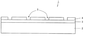
種基板1は、図1に示すように、下地となる下地基板2上に、バッファ層(図示しない)を介してIII 族窒化物半導体層3が形成され、III 族窒化物半導体層3上にマスク4が形成された構成である。マスク4には、ドット状に複数の窓5が空けられており、この窓5からIII 族窒化物半導体層3表面を露出させることで、種結晶領域(すなわちIII 族窒化物半導体をエピタキシャル成長させる起点となるIII 族窒化物半導体層3の表面)をドット状に点在させている。
In the
このように種結晶領域をドット状に点在させることで、結晶育成初期においてIII 族窒化物半導体を横方向成長させ、転位を曲げることで転位密度を低減して結晶品質を向上させることができる。また、結晶育成終了後に種基板1と育成したIII 族窒化物半導体結晶との分離を容易とすることができる。
By interspersing the seed crystal regions in a dot shape in this way, the group III nitride semiconductor can be laterally grown at the initial stage of crystal growth, and the dislocations can be bent to reduce the dislocation density and improve the crystal quality. .. In addition, it is possible to facilitate the separation of the
なお、III 族窒化物半導体層3をエッチング等して溝を形成することにより、種結晶領域をドット状に点在させてもよい。
The seed crystal regions may be interspersed in dots by forming grooves by etching the group III
マスク4は、ALD法(原子層堆積法)、CVD法(化学気相成長法)、スパッタなど任意の方法によって形成することができるが、特にALD法により形成することが望ましい。緻密で均一な厚さに形成することができ、フラックス法による育成中においてマスクが溶解してしまうのを抑制することができる。マスク4の材料は、フラックスに対して耐性を有し、そのマスク4からはIII 族窒化物半導体が成長しないような材料であればよい。たとえば、Al2 O3 、TiO2 、ZrO2 などを用いることができる。マスク4の厚さは、10nm以上500nm以下とすることが望ましい。
The
マスク4の窓5の配置パターンは、周期的なパターンが望ましい。特に、図2のように正三角形の三角格子状のパターンが望ましく、正三角形の各辺の方位は、III 族窒化物半導体層3のm軸<10−10>とすることが望ましい。窓5をこのような配置パターンとすることで、各種結晶領域からIII 族窒化物半導体が均質に育成し、III 族窒化物半導体の結晶品質の向上を図ることができる。
The arrangement pattern of the
各窓5の形状は、円、三角形、四角形、六角形など任意の形状でよいが、円または正六角形とすることが好ましい。各窓5に露出するIII 族窒化物半導体層3表面からの結晶成長をより均一とするためである。また、正六角形とする場合、その各辺の方位はIII 族窒化物半導体層3のm面とすることが望ましい。
The shape of each
窓5の直径W1は、10μm以上2000μm以下とすることが望ましい。また、窓5の間隔(輪郭と輪郭の最近接距離)W2は、10μm以上2000μm以下とすることが望ましい。W1、W2をこのような範囲とすることで、III 族窒化物半導体結晶の育成終了後の種基板との分離が容易となる。
The diameter W1 of the
下地基板2の材料は、その表面にIII 族窒化物半導体を育成可能な任意の材料でよい。ただし、Siを含まない材料が好ましい。混合融液中にSiが溶けだすと、III 族窒化物半導体の結晶成長を阻害してしまうためである。たとえば、サファイア、ZnO、スピネルなどを用いることができる。
The material of the
下地基板2の大きさは、直径2インチ以上が好ましい。下地基板2が大きくなるほど未成長領域や異常粒成長領域が発生しやすくなるため、本発明によってそれらの領域を抑制する効果が高まる。直径3インチ以上とする場合に本発明は特に効果的である。
The size of the
下地基板2上のIII 族窒化物半導体層3は、結晶成長させるIII 族窒化物半導体と同一組成の材料とすることが望ましい。特に、GaNとすることが望ましい。また、III 族窒化物半導体層3はMOCVD法、HVPE法、MBE法など、任意の方法によって成長させたものでよいが、結晶性や成長時間などの点でMOCVD法やHVPE法が好ましい。
It is desirable that the group III
III 族窒化物半導体層3の厚さは、2μm以上とすることが望ましい。フラックス法では、結晶育成初期においてIII 族窒化物半導体層3がメルトバックする可能性があるため、III 族窒化物半導体層3が完全に除去されて下地基板2が露出しない厚さとする必要があるためである。ここでメルトバックは、III 族窒化物半導体が混合融液中に溶解して除去されることをいう。ただし、III 族窒化物半導体層3が厚すぎると、種基板1に反りが発生してしまうため10μm以下の厚さとすることが望ましい。
The thickness of the group III
(結晶製造装置の構成)
本発明のIII 族窒化物半導体の製造方法では、たとえば以下の構成の結晶製造装置を用いる。
(Structure of crystal manufacturing equipment)
In the method for producing a group III nitride semiconductor of the present invention, for example, a crystal manufacturing apparatus having the following configuration is used.
図3は、フラックス法によるIII 族窒化物半導体の製造に用いる結晶製造装置10の構成を示した図である。図3のように、結晶製造装置10は、圧力容器20と、反応容器11と、坩堝12と、加熱装置13と、供給管14、16と、排気管15、17と、を有している。
FIG. 3 is a diagram showing the configuration of a
圧力容器20は、円筒形のステンレス製であり、耐圧性を有している。また、圧力容器20には、供給管16、排気管17が接続されている。圧力容器20の内部には、反応容器11と加熱装置13とが配置されている。このように反応容器11を圧力容器20の内部に配置しているため、反応容器11にさほど耐圧性が要求されない。そのため、反応容器11として低コストのものを使用することができ、再利用性も向上する。
The
反応容器11はSUS製であり耐熱性を有している。反応容器11内には、坩堝12が配置される。坩堝12の材質は、たとえばW(タングステン)、Mo(モリブデン)、BN(窒化ホウ素)、アルミナ、YAG(イットリウムアルミニウムガーネット)などである。坩堝12には、アルカリ金属とIII 族金属の混合融液21が保持され、混合融液21中には種基板1が収容される。
The
反応容器11には、供給管14、排気管15が接続されており、供給管14、排気管15に設けられた弁(図示しない)により反応容器11内の換気、窒素を含むガスの供給、反応容器11内の圧力の制御、を行う。また、圧力容器20にも供給管16より窒素を含むガスが供給され、供給管16、排気管17の弁(図示しない)でガスの供給量、排気量を調整することで、圧力容器20内の圧力と反応容器11内の圧力とがほぼ同じになるよう制御する。また、加熱装置13により、反応容器11内の温度を制御する。
A
また、結晶製造装置10には、坩堝12を回転させて坩堝12中に保持される混合融液21を攪拌することができる装置が設けられている。そのため、III 族窒化物半導体結晶の育成中に混合融液21を撹拌して混合融液21中のアルカリ金属、III 族金属、窒素の濃度分布が均一となるようにすることができる。これにより、III 族窒化物半導体結晶を均質に育成することができる。坩堝12を回転させる装置は、反応容器11内部から圧力容器20外部まで貫通する回転軸22と、反応容器11の内部に回転軸22と連結されて配置され、坩堝12を保持するターンテーブル23と、回転軸22の回転を制御する駆動装置24と、によって構成されている。この駆動装置24による回転軸22の回転によってターンテーブル23を回転させ、ターンテーブル23上に保持されている坩堝12を回転させる。
Further, the
なお、反応容器11として耐圧性を有したものを使用すれば、必ずしも圧力容器20は必要ではない。また、結晶育成中のアルカリ金属の蒸発を防止するために、坩堝12には蓋を設けてもよい。また、坩堝12の回転に替えて、あるいは加えて、坩堝12を揺動させる装置を設けてもよい。また、圧力容器20と反応容器11の二重容器としているが、三重容器として育成条件(温度、圧力など)のさらなる安定化を図ってもよい。
If a
(III 族窒化物半導体の製造方法)
次に、本発明のIII 族窒化物半導体の製造方法について、図4を参照に説明する。
(Manufacturing method of group III nitride semiconductor)
Next, the method for producing the group III nitride semiconductor of the present invention will be described with reference to FIG.
まず、酸素や露点など雰囲気が制御されたグローブボックス内で所定量のアルカリ金属、III 族金属、炭素を計量する。坩堝12内に種基板1を配置した後、計量した所定量のアルカリ金属、III 族金属を坩堝12に投入する。その坩堝12を搬送容器に格納して、大気に晒すことなく反応容器11内のターンテーブル23上に配置する。
First, weigh a predetermined amount of alkali metal, group III metal, and carbon in a glove box where the atmosphere such as oxygen and dew point is controlled. After arranging the
ここで、反応容器11内に、結晶成長開始時に混合融液21に接触しないように炭素を配置する。その方法の1つは、坩堝12の外に炭素を配置する方法である。反応容器11内であって坩堝12の外であれば、炭素はどこに配置されていてもよい。要は、混合融液21と接する雰囲気を共有する範囲内であればよい。たとえば、坩堝12の蓋12Aの上に炭素を配置する(図7、図11参照)。図7では、粉末状の炭素30を保持容器である坩堝31に入れて蓋12Aの上に配置している。図11に示すように、坩堝31を用いずに蓋12A上に直接、炭素30を配置してもよい。この場合、図12に示すように、坩堝31の上端面と蓋12Aとの間にスペーサ43を用いてギャップ44を形成しても良い。ギャップ44の幅により、炭素の坩堝12内への導入量を制御することができる。炭素は、たとえば粉末状、塊状のグラファイトである。粉末状の炭素を用いる場合には、飛散しないようにSUS、Mo(モリブデン)、W(タングステン)などの高温に耐えうる材料のメッシュに包んで配置するとよい。具体的には、フラックス法での結晶成長圧力において融点が結晶成長温度よりも高く、窒素やアルカリ金属、炭素などと反応しない材料のメッシュを用いる。坩堝12の蓋に替えてこのメッシュで坩堝12の開口部を覆い、その上に炭素を配置してもよい。なお、坩堝12と坩堝31全体を一回り大きな容器32に入れて蓋33をしてもよい(図9参照)。これにより、混合融液21に炭素を添加する効率がさらに向上する。
Here, carbon is arranged in the
また、たとえば、種基板1と混合融液21を保持する坩堝12とは別に坩堝31を用意し、その坩堝31に炭素30を投入し、坩堝12と炭素30を投入した坩堝31とを近接して配置する(図8参照)。この方法によれば、2つの坩堝12、31の距離によって、簡易に混合融液21への炭素の添加量を調整することができる。また、坩堝31に蓋を設け、その蓋の隙間の空け方によって、混合融液21への炭素の添加量と添加のタイミングを調整することも可能である。なお、混合融液21を保持した坩堝12を複数設け、1つの坩堝31から複数の坩堝12内へと炭素を添加するようにしてもよい。図10に、坩堝12を2つ設けた場合を示す。
Further, for example, a
他の方法としては、溶媒を混ぜてペースト状とした炭素を坩堝12の側壁上部に塗布しておく、坩堝12の蓋の裏側に炭素を張り付けたり、つり下げておくなどの方法を用いることができる。
As another method, carbon mixed with a solvent to form a paste may be applied to the upper part of the side wall of the
配置する炭素の適切な量は、原料や炭素の配置方法によって大きく影響されるため、それらを考慮して適宜調整することが望ましい。また、配置する炭素量は、従来のように混合融液21に直接炭素を添加する方法に比べて、多くの量が必要となる。坩堝12内の混合融液21と炭素は空間的に分離しており、炭素の一部が混合融液21に作用するためである。たとえば、アルカリ金属に対して3.0mol%以上とするのがよい。時間の経過によって十分な量の炭素を混合融液21へと添加することができる。
Since the appropriate amount of carbon to be arranged is greatly affected by the raw material and the carbon arrangement method, it is desirable to make appropriate adjustments in consideration of them. Further, the amount of carbon to be arranged is required to be larger than that of the conventional method of directly adding carbon to the
その後、反応容器11を密閉し、さらに反応容器11を圧力容器20内に密閉する。そして、圧力容器20内を真空引きした後、昇圧、昇温する。このとき、窒素を含むガスを反応容器11内部に供給する。
After that, the
次に、反応容器11内を結晶成長温度、結晶成長圧力まで上昇する。結晶成長温度は700℃以上1000℃以下、結晶成長圧力は2MPa以上10MPa以下である。このとき、坩堝12内のアルカリ金属、III 族金属は融解し、混合融液21を形成する。また、坩堝12を回転させることで混合融液21を攪拌し、混合融液21中のアルカリ金属とIII 族金属の分布が均一になるようにする。ただし、上記のようにして炭素30を配置しているため、この時点では炭素源(グラファイト粉末など)は混合融液21に接触していない。
Next, the inside of the
窒素が混合融液21に溶解していき、過飽和状態となると、種基板1の窓5に露出するIII 族窒化物半導体層3表面から、III 族窒化物半導体結晶6が六角錐状にエピタキシャル成長する(図4(a)参照)。各種結晶領域から育成した六角錐状のIII 族窒化物半導体結晶6は、横方向成長を主体として六角柱状に成長していき、隣接する六角柱状の結晶同士が合体し、平坦な表面を有する1つのIII 族窒化物半導体結晶6となる(図4(b)参照)。このとき、成長は横方向が支配的であるため、III 族窒化物半導体中の転位は横方向に曲げられる。そのため、転位密度が低減され、結晶性が向上する。
When nitrogen dissolves in the
このIII 族窒化物半導体結晶6の育成において、上記のように炭素30を配置しているため、結晶成長初期には混合融液21に炭素が添加されていない。しかし、時間の経過とともに次第に混合融液21に炭素が添加されていき、混合融液21中の炭素量が増加していく。その結果、III 族窒化物半導体結晶6の成長速度も次第に速くなっていく。坩堝12の外に配置された炭素30が具体的にどのようなルートで混合融液21に添加されるのかは不明であるが、窒素を含むガスや蒸発したアルカリ金属を含む雰囲気を介して、炭素自体あるいは炭素との反応物が坩堝12内へと運ばれ、混合融液21に添加されていると推察される。
In the growth of the group III
このように、本発明のIII 族窒化物半導体の製造方法では、結晶成長開始時には混合融液21への炭素の添加量は0であり、その後に次第に炭素の添加量が増加していくことになる。その結果、種基板1上のIII 族窒化物半導体結晶6は、未成長領域や異常粒成長領域が低減されている。また、炭素の添加量の増加に伴い、次第に成長速度も速くなっていくため、効率的にIII 族窒化物半導体結晶6を育成することができる。その理由は、以下のように推察される。
As described above, in the method for producing a group III nitride semiconductor of the present invention, the amount of carbon added to the
種結晶領域がドット状に点在された種基板1では、種基板1の全面を種結晶領域とする場合に比べて種結晶領域が小さく、種結晶領域とそうでない領域が混在している。そのため、混合融液21中に局所的な原料の濃度分布が発生していることが考えられる。その結果、全面を種結晶領域とする場合とはIII 族窒化物半導体の結晶育成に適した条件が異なっていると考えられる。
In the
そこで本発明では、炭素を混合融液21に接触しないように配置して、結晶成長初期には混合融液21に炭素が添加されていない状態としている。これにより、III 族窒化物半導体の結晶成長初期の過飽和度、あるいは成長の駆動力となる過剰な自由エネルギーが抑制され、種基板1の面積当たりの結晶成長の駆動力を適正に保つことができる。また、成長速度が抑制される結果、成長速度は均一化して異常粒成長する結晶がなくなり、混合融液中の原料(III 族金属、窒素)の濃度分布が均一となる。以上のように、混合融液21中の原料の濃度分布が減少し、かつIII 族窒化物半導体の成長レートが抑えられて均一化するため、種基板1上にIII 族窒化物半導体が結晶成長しない領域がなくなり、異常粒成長領域も減少したと考えられる。
Therefore, in the present invention, carbon is arranged so as not to come into contact with the
そして、次第に混合融液21に炭素が添加されて増加していき、成長速度も次第に速くなっていくので、本発明は効率的にIII 族窒化物半導体結晶6を育成することができる。また、III 族窒化物半導体結晶6の未成長領域や異常粒成長領域が低減された状態で、それを核としてさらに結晶成長が進むため、成長速度が速くなっても未成長領域や異常粒成長領域が新たに発生することはない。また、炭素は間接的に混合融液21へと供給されるため、混合融液21中の炭素濃度のばらつきが少なく、種基板1が局所的にメルトバックされることもなくなるため、III 族窒化物半導体結晶6の結晶品質もより向上させることができる。
Then, carbon is gradually added to the
また、次第に炭素の添加量が増加するため、アルカリ金属の坩堝12外への流出も抑制されると考えられる。発明者らの検討によると、混合融液21への炭素の添加量が少ないと、特にアルカリ金属に対して0.3mol%以下の炭素添加とすると、アルカリ金属が坩堝12の側壁を這い上がり、坩堝12の外に漏出する可能性が高くなることがわかった。アルカリ金属の漏出は、坩堝12の蓋の隙間に入り込んで蓋が開かなくなったり、III 族窒化物半導体結晶6の成長を不安定にするなどの問題がある。本発明によれば、このアルカリ金属の漏出を抑制でき、III 族窒化物半導体結晶6の育成を安定化することができる。
Further, since the amount of carbon added gradually increases, it is considered that the outflow of the alkali metal to the outside of the
その後、反応容器11の加熱を停止して温度を室温まで低下させ、圧力も常圧まで低下させ、III 族窒化物半導体の育成を終了する。ここで、種基板1のIII 族窒化物半導体層3上は窓5を空けたマスク4に覆われているため、育成したIII 族窒化物半導体結晶6は、窓5を介して部分的にIII 族窒化物半導体層3と接触しており、他の部分はマスク4と接触している。また、種基板1のマスク4と育成したIII 族窒化物半導体結晶6には線膨張係数差がある。そのため、育成終了時の降温において種基板1と育成したIII 族窒化物半導体結晶6とが自然に剥離する場合がある。また、剥離しなかったとしても、軽い衝撃を加えることで、種基板1と育成したIII 族窒化物半導体結晶6とを剥離させることができる(図4(c)参照)。
After that, the heating of the
育成したIII 族窒化物半導体結晶6を種基板1として、再度本発明のIII 族窒化物半導体の製造方法を用いてIII 族窒化物半導体結晶を育成してもよい。さらに高品質なIII 族窒化物半導体結晶を得ることができる。
The group III
以下、本発明の具体的な実施例について図を参照に説明するが、本発明は実施例に限定されるものではない。 Hereinafter, specific examples of the present invention will be described with reference to the drawings, but the present invention is not limited to the examples.
実施例1のGaNの製造方法について、図5、6を参照に説明する。 The method for producing GaN of Example 1 will be described with reference to FIGS. 5 and 6.
まず、育成に用いる種基板1を、次のようにして作製した。直径2インチ、厚さ1mmのサファイアからなる下地基板102を用意し、その下地基板102上に、MOCVD法によって、AlNからなるバッファ層(図示しない)、GaN層103を順に形成した(図5(a))。GaN層103の厚さは5μmとした。MOCVD法においては、窒素源には、アンモニア、Ga源には、トリメチルガリウム(Ga(CH3 )3 :TMG)、Al源には、トリメチルアルミニウム(Al(CH3 )3 :TMA)、キャリアガスには水素を用いた。
First, the
次に、ALD法を用いて、GaN層103上にAl2 O3 からなるマスク104を形成した(図5(b))。マスク104の厚さは0.1μmとした。
Next, a mask 104 made of Al 2 O 3 was formed on the
次に、フォトリソグラフィ、ウェットエッチングによってマスク104をパターニングし、三角格子状の配列パターンの窓105を形成した。これにより、窓105にGaN層103表面を露出させた(図5(c))。これにより、種結晶領域であるGaN層103表面をドット状に点在させた。窓105は直径W1が0.1mmの円とし、窓105と窓105の間隔W2は0.09mmとした。以上のようにして種基板1を作製した。
Next, the
次に、図11に示すように、種基板1を坩堝12に配置し、フラックス法を用いて種基板1上にIII 族窒化物半導体を育成した。結晶成長温度は860℃、結晶成長圧力は3MPaとし、アルカリ金属としてNaを16.7g、III 族金属としてGaを11.0g用い、供給するガスは窒素とした。また、図11に示すように、Cの粉末30をW(タングステン)のメッシュ40に包み、坩堝12の蓋12Aの上に配置した。なお、坩堝12と蓋12Aとは密着しておらず、両者間には微小隙間があり、ガスが坩堝12内に導入される。坩堝12と蓋12Aとの間に微小間隙があるのは、実施例2、3、4においても同じである。育成時間は40時間とした。また、坩堝12はアルミナ製のものを用いた。これにより、種基板1の各窓105に露出する各GaN層103からGaN結晶106を育成し、各GaN結晶106を合体させて一体とし、種基板1上に平坦な表面を有した1つのGaN結晶106を育成した(図6(a)参照)。
Next, as shown in FIG. 11, the
育成終了後、室温まで冷却されるのを待ってから坩堝12を取り出し、エタノール等でNa、Gaを取り除いた。GaN結晶106は種基板1から剥離しており、クラックなく自立されていた(図6(b)参照)。GaN結晶の成長速度は8μm/hであった。
After the growth was completed, the
(比較例1)
比較例1として、実施例1と同一構成の種基板1を用い、以下の点を変えた以外は同一の育成条件のフラックス法によって、種基板1上にGaN結晶を育成した。坩堝12にCをNaに対して0.6mol%直接投入した。各種結晶領域から育成したGaN結晶は合体して一体となっており、GaN結晶の成長速度は13μm/hであった。
(Comparative Example 1)
As Comparative Example 1, a
(比較例2)
比較例2として、実施例1と同一構成の種基板1を用い、以下の点を変えた以外は同一の育成条件のフラックス法によって、種基板1上にGaN結晶を育成した。比較例2では坩堝12に炭素を添加せず、坩堝12の外にも炭素を配置しないで育成を行った。各種結晶領域から育成したGaN結晶は合体して一体となっており、GaN結晶の成長速度は2μm/hであった。
(Comparative Example 2)
As Comparative Example 2, a
実施例1により育成したGaN結晶106と、比較例1、2により育成したGaN結晶とを、目視と光学顕微鏡により観察し対比した。その結果、比較例1により育成したGaN結晶は、未成長領域や異常粒成長領域、インクルージョン(結晶に内包された混合融液で主としてNaからなる)が多く含まれており、GaN結晶表面は凹凸が大きかった。また、比較例2により育成したGaN結晶は、各種結晶領域からほぼ均一に六角柱状に結晶成長しており、GaN結晶表面の凹凸は少なく、周期的であった。しかし、一部十分に結晶成長せずに結晶が合体していないところがあり、また種基板1の洗浄工程において剥離したと考えられるドット状の空孔が結晶中に見られた。また、比較例2のGaN結晶は薄く、育成の効率が悪かった。
The
一方、実施例1により育成したGaN結晶106は、比較例2に比べるとGaN結晶106表面の凹凸は若干大きいが、周期的であり、面内の凹凸分布は小さく良好であった。また、各種結晶領域からの結晶成長は均一であり、成長も十分に進んでいるため、各結晶が合体していない領域はなく、連続的で一体の結晶となっていた。また、種基板1の洗浄による剥離と考えられるドット状の結晶の空孔は見られなかった。また、比較例2に比べてGaN結晶106は厚く、効率的にGaN結晶106が育成できていた。
On the other hand, in the
実施例1と比較例1、2とを対比すると、実施例1では結晶育成初期は混合融液21にCが添加されておらず、未成長領域や異常粒成長領域が低減され、表面平坦性の高いGaN結晶106を育成できることがわかり、歩留りが劇的に向上することがわかった。また、窓5に露出する各種結晶領域からのGaN結晶106の成長が均一となり、育成したGaN結晶106の表面平坦性が向上することがわかった。また、実施例1では、時間の経過によって次第に混合融液21へCが添加されていくため、結晶成長速度が上昇して効率的にGaN結晶106を育成できることがわかった。
Comparing Example 1 with Comparative Examples 1 and 2, in Example 1, C was not added to the
実施例1における種基板1に変えて、GaNからなる自立基板を種基板として用い、実施例1と同様にして種基板上にGaN結晶を育成した。ただし、種基板上にはマスク104は形成されていない。育成したGaN結晶を目視と光学顕微鏡により観察したところ、未成長領域や異常粒成長領域、インクルージョンはほとんど見られなかった。また、GaN結晶表面の凹凸も少なく、表面平坦性が高かった。また、GaN結晶の厚さも実施例1と同等であり、効率的にGaN結晶を育成することができた。
Instead of the
実施例1における種基板1に変えて、種基板1においてマスク4を設けない構造の種基板を用いた。つまり、GaN層103の全面が露出したテンプレート基板を用いた。それ以外は実施例1と同様にして、種基板上にGaN結晶を育成した。育成したGaN結晶を目視と光学顕微鏡により観察したところ、実施例2と同様に、未成長領域や異常粒成長領域、インクルージョンはほとんど見られなかった。また、GaN結晶表面の凹凸も少なく、表面平坦性が高かった。また、GaN結晶の厚さも実施例1と同等であり、効率的にGaN結晶を育成することができた。
Instead of the
種基板1と混合融液21を保持するための坩堝12とは別途、図8に示すように、炭素を保持するための坩堝31を用意した。この坩堝31内には炭素の粉末30を入れた。本実施例では、実施例1−3と異なり、粉末30はメッシュ40で包まれていない。坩堝12と炭素を入れた坩堝31を近接して配置し、この状態で実施例1と同様にして、種基板1上にGaN結晶を育成した。育成したGaN結晶を目視と光学顕微鏡により観察したところ、実施例1と同様に未成長領域や異常粒成長領域、インクルージョンはほとんど見られなかった。また、GaN結晶の厚さも実施例1と同等であり、効率的にGaN結晶を育成することができた。
Separately from the
この実施例4のGaN結晶の製造方法では、坩堝12と炭素の粉末30を入れた坩堝31との距離を調整することによって、混合融液21への炭素の添加量を調整できる利点がある。
また、図7に示すように、炭素の粉末30を入れた坩堝31を蓋12Aの上に設けて、同様にGaNの成長を行っても、同様に実施例1と同一の効果が得られる。
The method for producing a GaN crystal of Example 4 has an advantage that the amount of carbon added to the
Further, as shown in FIG. 7, even if the
本実施例においては、図5(c)に示す実施例1と同一構造の基板を用いた。すなわち、基板には、サファイア基板上にGaNをエピタキシャル成長させた基板上にパターン化されたマスクの形成された基板を用いた。坩堝12内の原料の重量、成長温度は圧力等の条件は実施例1と同一である。種基板1と混合融液21を保持するための坩堝12とは別に、図12に示すように、炭素を保持するための坩堝31を用意した。この坩堝31内には炭素の粉末30を入れた。粉末30はメッシュ40で包まれていない。坩堝12の上端面には、坩堝12の軸に垂直な断面において120度間隔の3箇所にスペーサ43が設けられている。このスペーサ43により、坩堝12の上端面と蓋12Aとの間には1mmのギャップ44が形成される。この状態で実施例1と同様にして、種基板1上にGaN結晶を育成した。GaNの成長速度は11.3μm/hであった。育成したGaN結晶を目視と光学顕微鏡により観察したところ、極微量(4mg)の雑晶が観測された。
In this example, a substrate having the same structure as that of Example 1 shown in FIG. 5C was used. That is, as the substrate, a substrate in which a mask patterned on a substrate obtained by epitaxially growing GaN on a sapphire substrate was used was used. Conditions such as the weight of the raw material in the
比較のために、坩堝12の上端面と蓋12Aとの間に1mmのギャップ44が形成された坩堝12を用いて、坩堝12の中に炭素の粉末を入れて、GaNを成長させた。成長速度は11.6μm/hであり、雑晶は観測されなかった。このことから、炭素の粉末を坩堝12の外部において、坩堝12と蓋12Aとの間に積極的にギャップ44を設けても、良質なGaNの結晶を得ることができた。
坩堝12の上端面と蓋12Aとの間のギャップ44の幅は、0.2〜10mmが適切である。このギャップ44の幅が大き過ぎると、蒸発したNaが坩堝12の外に出る量が増えるために、育成中の融液のNaの量が低下する。そのため、ギャップ44の幅は、育成温度、圧力に応じて、適切に設定されることが望ましい。
意図的(積極的に)にギャップ44を設けることで、実施例1の場合に比べて、坩堝12内への炭素の流入量は増加するが、炭素の粉末を坩堝12の外部に設けることで、良質なGaN結晶を得ることができる。このギャップ44の幅を変化させることにより、炭素の坩堝12内への導入量を制御することができる。また、図13に示すように、坩堝12の上端面と蓋12Aとの間にギャップ44を設けて、炭素の粉末30を入れた坩堝31を、実施例4と同様に、坩堝12の設置面と同一面上に設けても良い。この場合にも、同様に良質なGaN結晶が得られる。
For comparison, a
The width of the
By intentionally (aggressively) providing the
(変形例)
実施例1では、育成開始時に混合融液に接触しないように炭素を配置し、これにより、育成開始前に混合融液の炭素濃度が0であって育成開始後に混合融液の炭素濃度が次第に増加するようにしているが、本発明はこれに限るものではない。育成開始前に混合融液の炭素濃度を0とし、育成開始後に混合融液の炭素濃度を次第に増加させる方法であれば、任意の方法を用いることができる。炭素濃度の増加は連続的であることが好ましい。なお、上記において炭素濃度が0とは、完全に炭素濃度が0であることを意味するのではなく、意図的な炭素の添加であると判別できない程度に炭素濃度が低ければよい。
(Modification example)
In Example 1, carbon was arranged so as not to come into contact with the mixed melt at the start of growing, so that the carbon concentration of the mixed melt was 0 before the start of growing and the carbon concentration of the mixed melt gradually increased after the start of growing. Although the number is increased, the present invention is not limited to this. Any method can be used as long as the carbon concentration of the mixed melt is set to 0 before the start of growth and the carbon concentration of the mixed melt is gradually increased after the start of growth. The increase in carbon concentration is preferably continuous. In the above, the carbon concentration of 0 does not mean that the carbon concentration is completely 0, but it is sufficient that the carbon concentration is so low that it cannot be determined that the carbon is intentionally added.
また、本発明は、ディッピング法などのように、育成初期において種結晶と混合融液とが分離され、その後種結晶を混合融液に接触させる方法にも適用することができる。この場合、混合融液中の炭素濃度の均一性がよいという利点がある。 The present invention can also be applied to a method in which the seed crystal and the mixed melt are separated at the initial stage of growth and then the seed crystal is brought into contact with the mixed melt, such as a dipping method. In this case, there is an advantage that the uniformity of the carbon concentration in the mixed melt is good.
本発明により育成したIII 族窒化物半導体は、III 族窒化物半導体からなる半導体素子の成長基板として利用することができる。 The group III nitride semiconductor grown according to the present invention can be used as a growth substrate for a semiconductor device made of a group III nitride semiconductor.
1:種基板
2:下地基板
3:III 族窒化物半導体層
4:マスク
5:窓
6:III 族窒化物半導体結晶
12:坩堝
21:混合融液
30:炭素
31:坩堝
40:メッシュ
43:スペーサ
44:ギャップ
1: Seed substrate 2: Base substrate 3: Group III nitride semiconductor layer 4: Mask 5: Window 6: Group III nitride semiconductor crystal 12: Crucible 21: Mixed melt 30: Carbon 31: Crucible 40: Mesh 43: Spacer 44: Gap
Claims (12)
前記種基板と前記混合融液の保持のための、蓋を有した第1の坩堝を用い、
炭素を、前記III 族窒化物半導体の成長初期において前記混合融液に接触しないように、前記第1の坩堝の前記蓋の上に配置し、
育成開始前に前記混合融液の炭素濃度を0とし、育成開始後に前記混合融液の炭素濃度を増加させながら、前記種基板上にIII 族窒化物半導体を成長させる、
を有することを特徴とするIII 族窒化物半導体の製造方法。 In a method for producing a group III nitride semiconductor in which a group III nitride semiconductor is grown by a flux method using a mixed melt of an alkali metal and a group III metal on a seed substrate.
Using a first crucible with a lid for holding the seed substrate and the mixed melt,
Carbon is placed on the lid of the first crucible so as not to come into contact with the mixed melt in the early stage of growth of the group III nitride semiconductor.
The carbon concentration of the mixed melt is set to 0 before the start of growth, and the group III nitride semiconductor is grown on the seed substrate while increasing the carbon concentration of the mixed melt after the start of growth.
A method for producing a group III nitride semiconductor, which comprises.
W(タングステン)、Mo(モリブデン)、BN(窒化ホウ素)、アルミナ、又は、YAG(イットリウムアルミニウムガーネット)から成り、前記種基板と前記混合融液の保持のための第1の坩堝を用い、
前記第1の坩堝を反応容器の内部に設け、
前記反応容器を反応容器の外部に設けられた加熱装置により加熱し、
所定量の計量され、育成開始後に前記混合融液の炭素濃度を増加させるための炭素を、前記III 族窒化物半導体の成長初期においては、前記混合融液に接触しないように、前記反応容器内の任意の位置に設け、
育成開始前に前記混合融液の炭素濃度を0とし、育成開始後に前記混合融液の炭素濃度を増加させながら、前記種基板上にIII 族窒化物半導体を成長させる、
を有することを特徴とするIII 族窒化物半導体の製造方法。 In a method for producing a group III nitride semiconductor in which a group III nitride semiconductor is grown by a flux method using a mixed melt of an alkali metal and a group III metal on a seed substrate.
Consisting of W (tungsten), Mo (molybdenum), BN (boron nitride), alumina, or YAG (yttrium aluminum garnet), using the seed substrate and a first crucible for holding the mixed melt.
The first crucible is provided inside the reaction vessel, and the first crucible is provided.
The reaction vessel is heated by a heating device provided outside the reaction vessel, and the reaction vessel is heated.
A predetermined amount of carbon for increasing the carbon concentration of the mixed melt after the start of growth is measured in the reaction vessel so as not to come into contact with the mixed melt at the initial stage of growth of the group III nitride semiconductor. Provided at any position of
The carbon concentration of the mixed melt is set to 0 before the start of growth, and the group III nitride semiconductor is grown on the seed substrate while increasing the carbon concentration of the mixed melt after the start of growth.
A method for producing a group III nitride semiconductor, which comprises.
前記種基板と前記混合融液の保持のための第1の坩堝を用い、
内部に前記混合融液を入れず、炭素を入れた第2の坩堝を、前記III 族窒化物半導体の成長初期において前記混合融液に接触させない状態に置き、
育成開始前に前記混合融液の炭素濃度を0とし、育成開始後に前記混合融液の炭素濃度を増加させながら、前記種基板上にIII 族窒化物半導体を成長させる、
を有することを特徴とするIII 族窒化物半導体の製造方法。 In a method for producing a group III nitride semiconductor in which a group III nitride semiconductor is grown by a flux method using a mixed melt of an alkali metal and a group III metal on a seed substrate.
Using the seed substrate and the first crucible for holding the mixed melt,
The second crucible containing carbon without the mixed melt was placed inside in a state where it was not in contact with the mixed melt at the initial stage of growth of the group III nitride semiconductor.
The carbon concentration of the mixed melt is set to 0 before the start of growth, and the group III nitride semiconductor is grown on the seed substrate while increasing the carbon concentration of the mixed melt after the start of growth.
A method for producing a group III nitride semiconductor, which comprises.
粉末状の炭素を、前記III 族窒化物半導体の成長初期において前記混合融液に接触させない状態に置き、
育成開始前に前記混合融液の炭素濃度を0とし、育成開始後に前記混合融液の炭素濃度を増加させながら、前記種基板上にIII 族窒化物半導体を成長させる、
を有することを特徴とするIII 族窒化物半導体の製造方法。 In a method for producing a group III nitride semiconductor in which a group III nitride semiconductor is grown by a flux method using a mixed melt of an alkali metal and a group III metal on a seed substrate.
The powdered carbon is placed in a state where it is not in contact with the mixed melt in the early stage of growth of the group III nitride semiconductor.
The carbon concentration of the mixed melt is set to 0 before the start of growth, and the group III nitride semiconductor is grown on the seed substrate while increasing the carbon concentration of the mixed melt after the start of growth.
A method for producing a group III nitride semiconductor, which comprises.
前記マスクは、三角格子状に配列された複数の窓を有する、
ことを特徴とする請求項7に記載のIII 族窒化物半導体の製造方法。 The seed substrate has a base substrate, a group III nitride semiconductor layer located on the base substrate, and a mask located on the group III nitride semiconductor layer.
The mask has a plurality of windows arranged in a triangular lattice.
The method for producing a group III nitride semiconductor according to claim 7.
Applications Claiming Priority (2)
| Application Number | Priority Date | Filing Date | Title |
|---|---|---|---|
| JP2016174068 | 2016-09-06 | ||
| JP2016174068 | 2016-09-06 |
Publications (2)
| Publication Number | Publication Date |
|---|---|
| JP2018039720A JP2018039720A (en) | 2018-03-15 |
| JP6841191B2 true JP6841191B2 (en) | 2021-03-10 |
Family
ID=61282039
Family Applications (1)
| Application Number | Title | Priority Date | Filing Date |
|---|---|---|---|
| JP2017168243A Active JP6841191B2 (en) | 2016-09-06 | 2017-09-01 | Method for manufacturing group III nitride semiconductor |
Country Status (3)
| Country | Link |
|---|---|
| US (1) | US10329687B2 (en) |
| JP (1) | JP6841191B2 (en) |
| CN (1) | CN107794567B (en) |
Families Citing this family (2)
| Publication number | Priority date | Publication date | Assignee | Title |
|---|---|---|---|---|
| US9773889B2 (en) * | 2014-07-18 | 2017-09-26 | Taiwan Semiconductor Manufacturing Company Limited | Method of semiconductor arrangement formation |
| JP7072769B2 (en) * | 2018-03-02 | 2022-05-23 | 国立大学法人大阪大学 | Method for Producing Group III Nitride Crystal |
Family Cites Families (13)
| Publication number | Priority date | Publication date | Assignee | Title |
|---|---|---|---|---|
| US7063741B2 (en) * | 2002-03-27 | 2006-06-20 | General Electric Company | High pressure high temperature growth of crystalline group III metal nitrides |
| JP4622447B2 (en) * | 2004-01-23 | 2011-02-02 | 住友電気工業株式会社 | Method for manufacturing group III nitride crystal substrate |
| WO2006095536A1 (en) * | 2005-03-04 | 2006-09-14 | Ngk Insulators, Ltd. | Method of growing single crystal and single crystal growing apparatus |
| WO2007108498A1 (en) * | 2006-03-23 | 2007-09-27 | Ngk Insulators, Ltd. | Nitride single crystal manufacturing apparatus |
| KR101192061B1 (en) * | 2006-11-14 | 2012-10-17 | 고꾸리쯔 다이가꾸 호우징 오사까 다이가꾸 | GaN CRYSTAL PRODUCING METHOD, GaN CRYSTAL, GaN CRYSTAL SUBSTRATE, SEMICONDUCTOR DEVICE AND GaN CRYSTAL PRODUCING APPARATUS |
| JP2009280482A (en) * | 2008-04-25 | 2009-12-03 | Sumitomo Electric Ind Ltd | Self-supporting group-iii nitride single-crystal substrate and method for producing semiconductor device using the same |
| US8507364B2 (en) * | 2008-05-22 | 2013-08-13 | Toyoda Gosei Co., Ltd. | N-type group III nitride-based compound semiconductor and production method therefor |
| JP2012012259A (en) * | 2010-07-01 | 2012-01-19 | Ricoh Co Ltd | Nitride crystal and method for producing the same |
| JP5754191B2 (en) | 2011-03-18 | 2015-07-29 | 株式会社リコー | Method for producing group 13 nitride crystal and method for producing group 13 nitride crystal substrate |
| CN103243389B (en) * | 2012-02-08 | 2016-06-08 | 丰田合成株式会社 | Manufacture the method for group III nitride semiconductor monocrystalline and manufacture the method for GaN substrate |
| JP6015566B2 (en) * | 2013-06-11 | 2016-10-26 | 豊田合成株式会社 | Group III nitride semiconductor etching method, group III nitride semiconductor crystal manufacturing method, and GaN substrate manufacturing method |
| JP6265995B2 (en) * | 2014-03-10 | 2018-01-24 | 日本碍子株式会社 | Method for producing group 13 element nitride crystal |
| JP6183317B2 (en) * | 2014-08-08 | 2017-08-23 | 豊田合成株式会社 | Group III nitride semiconductor manufacturing method and group III nitride semiconductor wafer |
-
2017
- 2017-09-01 JP JP2017168243A patent/JP6841191B2/en active Active
- 2017-09-04 CN CN201710786253.XA patent/CN107794567B/en active Active
- 2017-09-06 US US15/696,269 patent/US10329687B2/en active Active
Also Published As
| Publication number | Publication date |
|---|---|
| US10329687B2 (en) | 2019-06-25 |
| CN107794567B (en) | 2020-09-25 |
| JP2018039720A (en) | 2018-03-15 |
| CN107794567A (en) | 2018-03-13 |
| US20180066378A1 (en) | 2018-03-08 |
Similar Documents
| Publication | Publication Date | Title |
|---|---|---|
| JP4647525B2 (en) | Method for producing group III nitride crystal | |
| JP6183317B2 (en) | Group III nitride semiconductor manufacturing method and group III nitride semiconductor wafer | |
| JP4489446B2 (en) | Method for producing gallium-containing nitride single crystal | |
| JP2009536605A (en) | A method and material for growing a group III nitride semiconductor compound containing aluminum. | |
| JP2001064098A (en) | Method and device for growing crystal, and group iii nitride crystal | |
| US10693032B2 (en) | Method for producing Group III nitride semiconductor, seed substrate and Group III nitride semiconductor crystal | |
| US9153439B2 (en) | Method for etching a group III nitride semiconductor, method for producing a group III nitride semiconductor crystal, and method for producing a GaN substrate | |
| JP6841191B2 (en) | Method for manufacturing group III nitride semiconductor | |
| JP5123423B2 (en) | Method for producing group III nitride compound semiconductor | |
| CN107190324A (en) | Group III-nitride crystallization manufacture method and containing RAMO4Substrate | |
| JP6848242B2 (en) | Method for manufacturing group III nitride semiconductor | |
| JP5426178B2 (en) | Method for producing group III metal nitride single crystal | |
| CN110219047B (en) | Method for producing group III nitride crystal | |
| JP4014411B2 (en) | Group III nitride crystal manufacturing method | |
| JP6841195B2 (en) | Method for manufacturing group III nitride semiconductor | |
| JP7264343B2 (en) | Group III nitride crystal production method and seed substrate | |
| JP2014237568A (en) | METHOD OF MANUFACTURING GROUP III NITRIDE SEMICONDUCTOR CRYSTAL, AND METHOD OF MANUFACTURING GaN SUBSTRATE | |
| JP7125246B2 (en) | Method for producing group III nitride semiconductor | |
| JP2020152582A (en) | Method for manufacturing group III nitride semiconductor | |
| JP6720888B2 (en) | Method for manufacturing group III nitride semiconductor | |
| RU2369669C2 (en) | Substrate for growing of epitaxial layers of gallium nitride | |
| JP2015157760A (en) | Group 13 nitride crystal and group 13 nitride crystal substrate | |
| JP6307818B2 (en) | Method for producing group 13 nitride crystal | |
| JP2017100944A (en) | Group 13 nitride crystal and group 13 nitride crystal substrate | |
| JP6337526B2 (en) | Method for producing group 13 nitride crystal |
Legal Events
| Date | Code | Title | Description |
|---|---|---|---|
| A621 | Written request for application examination |
Free format text: JAPANESE INTERMEDIATE CODE: A621 Effective date: 20191107 |
|
| A131 | Notification of reasons for refusal |
Free format text: JAPANESE INTERMEDIATE CODE: A131 Effective date: 20200707 |
|
| A977 | Report on retrieval |
Free format text: JAPANESE INTERMEDIATE CODE: A971007 Effective date: 20200709 |
|
| A521 | Written amendment |
Free format text: JAPANESE INTERMEDIATE CODE: A523 Effective date: 20200831 |
|
| TRDD | Decision of grant or rejection written | ||
| A01 | Written decision to grant a patent or to grant a registration (utility model) |
Free format text: JAPANESE INTERMEDIATE CODE: A01 Effective date: 20210119 |
|
| A61 | First payment of annual fees (during grant procedure) |
Free format text: JAPANESE INTERMEDIATE CODE: A61 Effective date: 20210201 |
|
| R150 | Certificate of patent or registration of utility model |
Ref document number: 6841191 Country of ref document: JP Free format text: JAPANESE INTERMEDIATE CODE: R150 |