JP6823573B2 - Power converter - Google Patents
Power converter Download PDFInfo
- Publication number
- JP6823573B2 JP6823573B2 JP2017178185A JP2017178185A JP6823573B2 JP 6823573 B2 JP6823573 B2 JP 6823573B2 JP 2017178185 A JP2017178185 A JP 2017178185A JP 2017178185 A JP2017178185 A JP 2017178185A JP 6823573 B2 JP6823573 B2 JP 6823573B2
- Authority
- JP
- Japan
- Prior art keywords
- power
- circuit
- power unit
- short
- capacitor
- Prior art date
- Legal status (The legal status is an assumption and is not a legal conclusion. Google has not performed a legal analysis and makes no representation as to the accuracy of the status listed.)
- Active
Links
Images


Description
本発明は、電力変換装置に関する。 The present invention relates to a power converter.
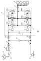
鉄道車両用電力変換装置の構成例を図2に示す。図2において、21は集電装置(パンタグラフ)、24は高速遮断器、25は断流器、26は充電抵抗、11はリアクトル、28は平滑コンデンサ、22はモータ、13’はインバータパワーユニット、23は車輪、27はレールである。 FIG. 2 shows a configuration example of the power conversion device for railway vehicles. In FIG. 2, 21 is a current collector (pantograph), 24 is a high-speed circuit breaker, 25 is a breaker, 26 is a charging resistor, 11 is a reactor, 28 is a smoothing capacitor, 22 is a motor, and 13'is an inverter power unit, 23. Is a wheel and 27 is a rail.
図2の回路の動作を説明する。架線から得られる直流電力は集電装置(パンタグラフ)21で集電され、高速遮断器24、断流器25及びリアクトル11を介してインバータパワーユニット13’に供給される。
The operation of the circuit of FIG. 2 will be described. The DC power obtained from the overhead wire is collected by the current collector (pantograph) 21 and supplied to the inverter power unit 13'via the high-
断流器25には、電源投入時の突入電流を抑制するために、並列に充電抵抗26が接続されている。リアクトル11は、主回路の一部が接地電位に短絡する、いわゆる地絡故障が発生した際に、変電所から過電流が流れ込まないように、電流の増加率di/dtを制限するために断流器25と直列に接続される。
A
インバータパワーユニット13’は、複数のパワー半導体モジュール2’(PU、NU、PV、NV、PW、NW)と、パワー半導体モジュール2’のゲートを制御するゲート駆動回路15と、直流電圧を安定化させるための平滑コンデンサ28を有する。インバータパワーユニット13’は、入力された直流電力を任意周波数・任意電圧の三相交流に変換し、モータ22を駆動する。また、インバータパワーユニット13’は、パワー半導体モジュール2’を冷却するために、図示しない冷却器を有する。
The inverter power unit 13'stabilizes a plurality of power semiconductor modules 2'(PU, NU, PV, NV, PW, NW), a
前記インバータパワーユニット13’では、パワー半導体として一般にSi(シリコン)を材料として使ったIGBT(Insulated Gate Bipolar Transistor)が広く使われている。IGBTをインバータパワーユニットに適用する場合、ゲート駆動回路やIGBT自体の誤動作によるアーム短絡を考慮した設計が必要となる。アーム短絡とは、電源ライン間に複数個直列接続されたIGBT、例えば図2ではパワー半導体モジュール2’(PU)とパワー半導体モジュール2’(NU)が、同時にオンすることにより、電源のプラスとマイナスが短絡されてしまう現象である。電源が短絡されると、半導体素子(IGBT)には平滑コンデンサ28から過大な電流が供給され破壊に至る。
In the inverter power unit 13', an IGBT (Insulated Gate Bipolar Transistor) that generally uses Si (silicon) as a material is widely used as a power semiconductor. When applying the IGBT to the inverter power unit, it is necessary to design in consideration of the arm short circuit due to the malfunction of the gate drive circuit and the IGBT itself. An arm short circuit means that a plurality of IGBTs connected in series between power supply lines, for example, the power semiconductor module 2'(PU) and the power semiconductor module 2'(NU) in FIG. 2 are turned on at the same time to increase the power supply. This is a phenomenon in which the minus is short-circuited. When the power supply is short-circuited, an excessive current is supplied to the semiconductor element (IGBT) from the
短絡が発生した場合にパワー半導体が破壊に至るまでの時間を短絡耐量という。この短絡耐量より短時間で短絡を検知してパワー半導体をオフし、電流を止めればパワー半導体を保護できる。鉄道車両の電力変換装置に使う1.7kV〜6.5kV耐圧のIGBTの場合には、一般に約10μs以上の短絡耐量があり、短絡保護回路で保護が可能である。 The time it takes for a power semiconductor to break when a short circuit occurs is called the short circuit tolerance. The power semiconductor can be protected by detecting a short circuit in a shorter time than this short circuit tolerance, turning off the power semiconductor, and stopping the current. In the case of an IGBT with a withstand voltage of 1.7 kV to 6.5 kV used for a power converter of a railway vehicle, it generally has a short-circuit withstand capacity of about 10 μs or more, and can be protected by a short-circuit protection circuit.
近年は、IGBTに代わってワイドバンドギャップ半導体であるSiC(炭化ケイ素)やGaN(窒化ガリウム)等を用いたパワー半導体が普及しつつある。ワイドバンドギャップ半導体は、損失が少ないという特長を持つ一方で、短絡耐量が短く(一般にSi−IGBTの1/2以下)、前述の短絡保護回路による保護が間に合わず、短絡保護回路の動作前に半導体素子が破壊されるという問題がある。 In recent years, power semiconductors using wide bandgap semiconductors such as SiC (silicon carbide) and GaN (gallium nitride) have become widespread in place of IGBTs. While wide-band gap semiconductors have the advantage of low loss, they have a short short-circuit tolerance (generally 1/2 or less of Si-IGBT), and the protection provided by the short-circuit protection circuit described above is not in time, so before the short-circuit protection circuit operates. There is a problem that the semiconductor element is destroyed.
この問題に対して、短絡時の電流の増加率di/dtを1/2以下に抑制するなどして破壊に至るまでの時間、すなわち短絡耐量を2倍以上に伸ばし、短絡保護回路による保護を可能とする手法が考えられる。 To solve this problem, the time until failure, that is, the short-circuit withstand capability, is doubled or more by suppressing the current increase rate di / dt at the time of short-circuit to 1/2 or less, and protection by the short-circuit protection circuit is provided. A method that enables it can be considered.
短絡時の電流の増加率は、平滑コンデンサの充電電圧Vccと、主回路インダクタンスLs(平滑コンデンサと2直列のパワー半導体、及びそれらを接続する配線のインダクタンスの合計)を用いて、以下の式(1)であらわされる。
di/dt=Vcc/Ls ・・・ (1)
The rate of increase of the current at the time of short circuit is calculated by the following equation (total of the charging voltage Vcc of the smoothing capacitor and the main circuit inductance Ls (the sum of the inductances of the smoothing capacitor and the power semiconductor in
di / dt = Vcc / Ls ... (1)
式(1)より、Lsを2倍以上に大きくするとdi/dtが1/2以下になり、短絡時の過電流を1/2以下に抑制できることから、短絡耐量を2倍以上に増やすことができることが分かる。一方で、Lsを2倍以上に大きくするとパワー半導体が電流を遮断する際の電流変化によってLsに発生する電圧が2倍以上に高くなり、ワイドバンドギャップ半導体に過電圧が印加され、破壊されてしまうため、Lsは単純には大きくできない。 From the equation (1), when Ls is increased more than twice, di / dt becomes 1/2 or less, and the overcurrent at the time of short circuit can be suppressed to 1/2 or less. Therefore, the short circuit withstand capacity can be increased more than twice. I know I can do it. On the other hand, if Ls is increased more than twice, the voltage generated in Ls becomes more than twice as high due to the change in current when the power semiconductor cuts off the current, and an overvoltage is applied to the wide bandgap semiconductor, resulting in destruction. Therefore, Ls cannot be simply increased.
di/dtを抑制する方法として、Vccを低減する方法も考えられる。このためには、平滑コンデンサの容量を少なくとも1/2以下に減らし、短絡が発生して過電流が流れた場合に、速やかに平滑コンデンサを放電させてVccを1/2以下に低減する必要がある。しかしながら、平滑コンデンサの容量を低減すると、通常のモータ駆動時に消費される電力により平滑コンデンサに発生するVccの変動分ΔVccが大きくなり、Vccに応じて制御しているモータの動作が不安定となって、モータの振動や車輪の空転などの問題を引き起こす。 As a method of suppressing di / dt, a method of reducing Vcc is also conceivable. For this purpose, it is necessary to reduce the capacity of the smoothing capacitor to at least 1/2 or less, and to quickly discharge the smoothing capacitor to reduce Vcc to 1/2 or less when a short circuit occurs and an overcurrent flows. is there. However, if the capacity of the smoothing capacitor is reduced, the fluctuation amount ΔVcc of Vcc generated in the smoothing capacitor due to the power consumed during normal motor driving becomes large, and the operation of the motor controlled according to Vcc becomes unstable. This causes problems such as motor vibration and wheel slippage.
以上のように、ワイドバンドギャップ半導体を用いたインバータの場合には、短絡発生時に保護回路による保護が困難であるという問題があった。 As described above, in the case of an inverter using a wide bandgap semiconductor, there is a problem that it is difficult to protect by a protection circuit when a short circuit occurs.
本発明は、上記問題を解決する手段を提供するものであって、主回路インダクタンスを増やさず、制御安定性も損なうことなく、短絡時の短絡電流を抑制し、ワイドバンドギャップ半導体等を適用したインバータのアーム短絡の保護を可能とする鉄道用電力変換装置を提供することにある。 The present invention provides a means for solving the above problems, suppresses a short-circuit current at the time of a short circuit, does not increase the main circuit inductance, does not impair control stability, and applies a wide bandgap semiconductor or the like. The purpose of the present invention is to provide a power conversion device for railways that can protect an inverter arm short circuit.
本発明に係る電力変換装置は、直流電源に接続する一対の直流端子と、負荷に接続する交流端子と、複数のワイドバンドギャップ半導体素子から構成され直流電力を交流電力に変換する逆変換回路とワイドバンドギャップ半導体素子のスイッチング時に電荷を供給するために当該逆変換回路の入力側に接続されるスイッチング用コンデンサとを有するインバータパワーユニットと、一対の直流端子とインバータパワーユニットの入力側との間に設ける平滑化用コンデンサとを備え、スイッチング用コンデンサの容量は、平滑化用コンデンサの容量の1/2以下であり、平滑化用コンデンサとインバータパワーユニットとは、所定値以上のインダクタンスを有する配線を介して接続されることを特徴とする。 The power conversion device according to the present invention includes a pair of DC terminals connected to a DC power supply, an AC terminal connected to a load, and an inverse conversion circuit composed of a plurality of wideband gap semiconductor elements to convert DC power into AC power. A wide band gap is provided between an inverter power unit having a switching capacitor connected to the input side of the inverse conversion circuit to supply charge when switching the semiconductor element, and a pair of DC terminals and the input side of the inverter power unit. and a capacitor for smoothing the capacitance of the switching capacitor is less than half of the capacitance of the capacitor for smoothing, the capacitor and the inverter power unit for smoothing, via a wiring having a predetermined value or more inductance characterized in that it is connected.
本発明によれば、電力変換装置にワイドバンドギャップ半導体などの短絡耐量の短いパワー半導体素子が用いられる場合でも、システムの制御安定性を損なうことなく短絡保護が可能となる。前述した以外の構成及び効果は、以下の実施形態の説明により明らかにされる。 According to the present invention, even when a power semiconductor element having a short short circuit tolerance such as a wide bandgap semiconductor is used for the power conversion device, short circuit protection can be performed without impairing the control stability of the system. Configurations and effects other than those described above will be clarified by the description of the following embodiments.
以下、図面を用いて実施例1〜3について説明する。 Hereinafter, Examples 1 to 3 will be described with reference to the drawings.
図1は、実施例1に係る鉄道車両用の電力変換装置の構成を示す図である。図1において、図2に示す従来の鉄道車両用の電力変換装置と同じ構成要素については、同一の符号を付している。 FIG. 1 is a diagram showing a configuration of a power conversion device for a railway vehicle according to the first embodiment. In FIG. 1, the same components as those of the conventional power conversion device for railway vehicles shown in FIG. 2 are designated by the same reference numerals.
実施例1に係る電力変換装置が、図2に示す従来の鉄道車両用の電力変換装置と異なる点は、インバータパワーユニット13と、直流電圧を安定化させるための平滑化用コンデンサ14を有する。インバータパワーユニット13は、直流電力を交流に変換するための逆変換回路10と、スイッチング用コンデンサ12とを有する。
実施例1に係る電力変換装置は、架線20から供給される直流電力を任意周波数・任意電圧の三相交流に変換し、モータ(交流電動機)22に交流電力を供給するもので、架線20から供給される直流電力が端子対(P、N)に入力され、交流端子Aに接続されたモータ22に交流電力が供給される。
The power conversion device according to the first embodiment differs from the conventional power conversion device for railway vehicles shown in FIG. 2 in that it has an
The power conversion device according to the first embodiment converts the DC power supplied from the
また図1において、21は集電装置(パンタグラフ)、24は高速遮断器、25は断流器、26は充電抵抗、11はリアクトル、23は車輪、27はレールである。架線20から得られる直流電力は、パンタグラフ21で集電され、高速遮断器24と断流器25及びリアクトル11を介して端子対(P、N)に入力される。断流器25には電源投入時の突入電流を抑制するために、並列に充電抵抗26が接続されている。リアクトル11は、主回路の一部が接地電位に短絡する、いわゆる地絡故障が発生した際に変電所から過電流が流れ込まないように、電流の増加率di/dtを制限するために断流器と直列に接続される。
Further, in FIG. 1, 21 is a current collector (pantograph), 24 is a high-speed circuit breaker, 25 is a breaker, 26 is a charging resistor, 11 is a reactor, 23 is a wheel, and 27 is a rail. The DC power obtained from the
逆変換回路10は少なくとも、複数のパワー半導体モジュール2(PU、NU、PV、NV、PW、NW)と、これらパワー半導体モジュール2へ駆動信号を供給するゲート駆動回路15とを有する。また、逆変換回路10は、短絡発生時にパワー半導体モジュール2が破壊されることを防止するための短絡保護回路(非図示)も備えている。この短絡保護回路は、公知のインバータで用いられているものと同じ回路でよい。さらに、逆変換回路10には、これ以外の機器として、たとえばパワー半導体モジュール2を冷却するための冷却器を有していてもよい。
The
本実施例に係る電力変換装置と、図2に示す従来の電力変換装置との違いの1つは、本実施例に係る電力変換装置が、図2に記載の平滑コンデンサ28に代えて、2つのコンデンサ(スイッチング用コンデンサ12と平滑化用コンデンサ14)が備えている点である。
また、図1において、142は平滑化用コンデンサ14とインバータパワーユニット13との間の配線を表しており、この配線142は所定値以上の(寄生)インダクタンスを有する(以下では、この配線142による寄生のインダクタンスをLoと表記する)。なお、図1において、配線142は正極側(端子Pの存在する側)と負極側(端子Nの存在する側)に存在するが、正極側の配線と負極側の配線の(寄生)インダクタンスの合計がLoである。
One of the differences between the power conversion device according to this embodiment and the conventional power conversion device shown in FIG. 2 is that the power conversion device according to this embodiment replaces the smoothing
Further, in FIG. 1, 142 represents a wiring between the smoothing
本実施例に係る電力変換装置の有する逆変換回路10は、逆変換回路10を構成するパワー半導体モジュール2(PU、NU、PV、NV、PW、NW)として、SiC−MOSFET(Silicon-Carbide Metal-Oxide-Semiconductor Field-Effect Transistor)を用いている点が、従来の電力変換装置と異なる(図2に示す従来の電力変換装置は、パワー半導体モジュール2として、例えばIGBT(Insulated Gate Bipolar Transistor)を用いている)。ただし、それ以外の点、たとえば逆変換回路10の配置構成などは、従来の電力変換装置と同じである。
The
パワー半導体モジュール2は、SiC−MOSFETと、このSiC−MOSFETに逆並列に接続されたダイオードから構成される。なお、本実施例では、各パワー半導体モジュール2に用いられる半導体素子がSiC−MOSFETである例を説明するが、SiC−MOSFETに代えて、窒化ガリウム系材料やダイヤモンドなどのワイドバンドギャップ半導体を用いてもよいし、あるいはIGBTを用いてもよい。
The
本実施例の特徴は、従来の電力変換装置で用いられていた平滑コンデンサを、スイッチング用と平滑化用に分離して配置し、平滑化用コンデンサ14を所定値以上の(寄生)インダクタンスを有する配線142を介して逆変換回路10に接続した点にある。
The feature of this embodiment is that the smoothing capacitor used in the conventional power conversion device is arranged separately for switching and smoothing, and the smoothing
一般に、主回路に搭載されるコンデンサの総容量は、3000μF〜20000μF程度であり、直流電圧や接続されるモータの出力に合わせて選定される。 Generally, the total capacity of the capacitors mounted on the main circuit is about 3000 μF to 20000 μF, and is selected according to the DC voltage and the output of the connected motor.
ここで、本実施例のように、従来の電力変換装置が用いていた平滑コンデンサに代えて、スイッチング用コンデンサ12と平滑化用コンデンサ14との2つを設けたことによる効果について説明する。
図3(a)は、アーム短絡発生時にパワー半導体モジュール2(または2’)の半導体素子(SiC−MOSFETまたはIGBT)に流れる電流の時間変化の例を示す図である。図3(a)において、横軸は短絡が発生してからの経過時間を、縦軸は半導体素子に流れる電流の大きさを表す。また、点線は、従来の電力変換装置で短絡が発生した場合に半導体素子に流れる短絡電流を示し、実線は、本実施例に係る電力変換装置において短絡が発生した場合に半導体素子に流れる短絡電流を示す。
Here, the effect of providing two switching
FIG. 3A is a diagram showing an example of a time change of the current flowing through the semiconductor element (SiC-MOSFET or IGBT) of the power semiconductor module 2 (or 2') when an arm short circuit occurs. In FIG. 3A, the horizontal axis represents the elapsed time since the short circuit occurred, and the vertical axis represents the magnitude of the current flowing through the semiconductor element. The dotted line indicates the short-circuit current flowing through the semiconductor element when a short circuit occurs in the conventional power conversion device, and the solid line indicates the short-circuit current flowing through the semiconductor element when a short circuit occurs in the power conversion device according to the present embodiment. Is shown.
従来の電力変換装置(たとえば図2)では、インバータパワーユニット13’に用いられる平滑コンデンサ28がひとつの大容量コンデンサ、あるいは一箇所に集約された複数のコンデンサで構成されているため、短絡が発生するとそれらの全てのコンデンサの電荷が放電され、半導体素子に大きな電流が流れるため、点線に示すように、時刻t2にて発熱などにより半導体素子の破壊に至る。
In a conventional power converter (for example, FIG. 2), the smoothing
一方、本実施例に係る電力変換装置の場合には、短絡発生時にスイッチング用コンデンサ12と平滑化用コンデンサ14の両方から電流が流れ込むことになる。しかし、平滑化用コンデンサ14の方は、配線142の(寄生)インダクタンスを介して逆変換回路10に接続されているため、di/dtが制限され、電流値がスイッチング用コンデンサ12からの放電電流よりも小さくなるため、半導体素子に流れる全電流は従来よりも小さくなる。
また、スイッチング用コンデンサ12から大部分の電流が供給されるために、スイッチング用コンデンサ12が先に放電され、時刻t1で電流は減少に転じる。時刻t3に至ると、平滑化用コンデンサ14からの放電電流が、スイッチング用コンデンサ12の放電電流より大きくなるため、半導体素子に流れる電流は再び増加に転じる。この際の電流変化率di/dtは、配線142の(寄生)インダクタンスにより決まる値となる。時刻t4に至って、図1には図示していない短絡保護回路により電流が遮断され、半導体素子が破壊することなくシステムを停止できる。
On the other hand, in the case of the power conversion device according to the present embodiment, current flows from both the switching
Further, since most of the current is supplied from the switching
次に、図3(b)は、短絡が発生していない通常の動作状態の時に、半導体素子に流れる電流の波形の例を示す図である。図3(b)において、横軸は半導体素子に電流が流れ始めてからの経過時間を表し、縦軸は半導体素子に流れる電流の大きさを表す。また、図3(b)のグラフにおいて、点線は、本実施例に係る電力変換装置に短絡が発生した時の、半導体素子に流れる電流の波形を示し、一方実線は、正常動作時に半導体素子に流れる電流の波形を示す。
通常の動作状態では、負荷であるモータ22のインダクタンスが大きいため、di/dtが制限され電流の増加が緩やかになる。一般に、モータのインダクタンスは数mH程度あり、スイッチング用コンデンサ12や配線142の(寄生)インダクタンスより十分に大きいため、電流は、スイッチング用コンデンサ12及び平滑化用コンデンサ14の両方からほぼ均等に流れることになる。これにより、負荷のモータを駆動する際に、モータのトルク変動などによって発生する直流電圧の変動を、スイッチング用コンデンサ12と平滑化用コンデンサ14の両方で制限でき、十分な直流電圧のダンピング効果が得られる。
Next, FIG. 3B is a diagram showing an example of a waveform of a current flowing through a semiconductor element in a normal operating state in which a short circuit does not occur. In FIG. 3B, the horizontal axis represents the elapsed time from the start of current flowing through the semiconductor element, and the vertical axis represents the magnitude of the current flowing through the semiconductor element. Further, in the graph of FIG. 3B, the dotted line shows the waveform of the current flowing through the semiconductor element when the power conversion device according to the present embodiment is short-circuited, while the solid line shows the semiconductor element during normal operation. The waveform of the flowing current is shown.
In a normal operating state, since the inductance of the
ただし、スイッチング用コンデンサ12の容量、平滑化用コンデンサ14の容量及びこれらを接続する配線142の(寄生)インダクタンスは、適切に設定する必要がある。
However, the capacitance of the switching
まず、スイッチング用コンデンサ12は、短絡発生時に半導体素子に流れる電流を抑制できる値に設定する必要がある。ワイドバンドギャップ半導体の場合、半導体素子の構造設計にも依存するが、短絡耐量がシリコン素子(シリコンを材料とするIGBT等の半導体素子)の1/2〜1/10程度に減少するため、短絡電流も1/2〜1/10程度に抑制する必要がある。このため、スイッチング用コンデンサ12の容量は、インバータシステムとして必要な全容量、すなわち平滑化用コンデンサの容量の1/2以下にする必要がある。短絡耐量が1/10の半導体素子を適用する場合であれば、スイッチング用コンデンサ12の容量も、平滑化用コンデンサの容量の1/10に設定する。
First, the switching
次に、配線142の(寄生)インダクタンスLoは、短絡発生時の高いdi/dtの電流が素子に流れ込まないように、スイッチング用コンデンサ12と逆変換回路10内との電流経路上のインダクタンスLs(一般に、「主回路インダクタンス」と呼び、以下でも「主回路インダクタンスLs」という)よりも大きく、たとえばLsの2倍以上にする必要がある。特に短絡耐量を考慮すると、配線142の(寄生)インダクタンスLoは、少なくともLsの10倍程度に設定する必要がある。
Next, the (parasitic) inductance Lo of the
例えば、一例として、首都圏などを走行する電車に用いられる直流1500V架線用のインバータにおいて、短絡耐量がシリコンIGBTの1/2のSiC−MOSFETを用いた場合、スイッチング用コンデンサ、平滑化用コンデンサをいずれも3200μFとする。 For example, in an inverter for a DC 1500V overhead wire used for a train traveling in a metropolitan area or the like, when a SiC-MOSFET having a short circuit tolerance of 1/2 that of a silicon IGBT is used, a switching capacitor and a smoothing capacitor are used. Both are set to 3200 μF.
また、主回路インダクタンスLsは、一般に50nH〜200nH程度であることから、配線の(寄生)インダクタンスLoは、この10倍程度として500nH〜2000nH程度に設定するのが望ましい。この場合の配線長としては、50cm〜2m程度を選択すれば適切なLoを設定することができる。 Further, since the main circuit inductance Ls is generally about 50 nH to 200 nH, it is desirable to set the (parasitic) inductance Lo of the wiring to about 500 nH to 2000 nH as about 10 times this. As the wiring length in this case, an appropriate Lo can be set by selecting about 50 cm to 2 m.
図4は、実施例2に係る電力変換装置の構成を示す図である。図4において、図1に示す実施例1に係る電力変換装置と同じ構成要素には同一の符号を付してある。実施例2と実施例1との構成上の異なる点は、実施例2に係る電力変換装置では、架線から交流電力が供給される点、そしてそのために、パンタグラフ21とコンバータパワーユニット30の間に主変圧器33を設け、主変圧器33の2次側とインバータパワーユニット13の間に、交流を直流に変換するコンバータパワーユニット30を設けた点にある。
FIG. 4 is a diagram showing a configuration of a power conversion device according to a second embodiment. In FIG. 4, the same components as those of the power conversion device according to the first embodiment shown in FIG. 1 are designated by the same reference numerals. The structural difference between the second embodiment and the first embodiment is that in the power conversion device according to the second embodiment, AC power is supplied from the overhead wire, and therefore, mainly between the
実施例2に係る電力変換装置の動作を説明する。
交流の架線より得た交流電力を主変圧器33を介して降圧する。コンバータパワーユニット30は、降圧された交流電力を直流電力に変換し、コンバータパワーユニット30の後段にあるインバータパワーユニット13に供給する。コンバータパワーユニット30は、パワー半導体モジュール3(PU、NU、PV、NV)とゲート駆動回路15等で構成される順変換回路32と、スイッチング用コンデンサ31から構成される。インバータパワーユニット13は、任意の三相交流波形を生成し、モータを駆動する。インバータパワーユニット13の構成は、実施例1で説明したものと同じであるため、ここでの説明は略す。
The operation of the power conversion device according to the second embodiment will be described.
The AC power obtained from the AC overhead line is stepped down via the
コンバータパワーユニット30とインバータパワーユニット13の間には、平滑化用コンデンサ34が配置される。この平滑化用コンデンサ34の容量は、スイッチング用コンデンサ12及びスイッチング用コンデンサ31の容量の2倍以上とする。
また、スイッチング用コンデンサ12と平滑化用コンデンサ34との接続及びスイッチング用コンデンサ31と平滑化用コンデンサ34との接続については、それぞれ、コンバータパワーユニット30及びインバータパワーユニット13の主回路インダクタンスLsの10倍以上のインダクタンスLoを持った配線または導体バーで接続する。ここで、導体バーとは、配線に代り銅やアルミなどで構成した板状の配線のことである。
A smoothing
Further, regarding the connection between the switching
本実施例によれば、コンバータパワーユニット30及びインバータパワーユニット13に内蔵するスイッチング用コンデンサ31及び12の容量を、短絡耐量を確保するために必要な最小限の容量とし、モータ駆動の際に発生する直流電圧の脈動を抑制するために必要な容量を、コンバータパワーユニット30とインバータパワーユニット13との間に設けた平滑化用コンデンサ34にて確保する構成とする。
これにより、ワイドバンドギャップ半導体などの短絡耐量の低い半導体素子を使用した場合の短絡耐量を確保しつつ、スイッチング時の跳ね上がり電圧の増加を抑制できる。また、スイッチング用コンデンサ12または31と平滑化用コンデンサ34とを接続する配線の(寄生)インダクタンスLoをコンバータパワーユニット30及びインバータパワーユニット13の主回路インダクタンスLsの10倍程度に設定することにより、短絡発生時に平滑化用コンデンサからの短絡電流の流入を抑制でき、短絡耐量の低下を避けることができる。
According to this embodiment, the capacities of the switching
As a result, it is possible to suppress an increase in the flip-up voltage during switching while ensuring the short-circuit tolerance when a semiconductor element having a low short-circuit tolerance such as a wide bandgap semiconductor is used. Further, a short circuit occurs by setting the (parasitic) inductance Lo of the wiring connecting the switching
図5は、実施例3に係る電力変換装置の構成を示す図である。図5において、図1及び図4に示す実施例1及び2に係る電力変換装置と同じ構成要素には同一の符号を付してある。実施例3と実施例2との構成上の異なる点は、実施例3では補助電源用パワーユニットを追加した点にある。 FIG. 5 is a diagram showing a configuration of a power conversion device according to a third embodiment. In FIG. 5, the same components as those of the power conversion apparatus according to the first and second embodiments shown in FIGS. 1 and 4 are designated by the same reference numerals. The structural difference between the third embodiment and the second embodiment is that the auxiliary power supply power unit is added in the third embodiment.
実施例3に係る電力変換装置の動作を説明する。
交流の架線より得た交流電力を主変圧器33を介して降圧する。コンバータパワーユニット30は、降圧された交流電力を直流電力に変換し、コンバータパワーユニット30の後段にあるインバータパワーユニット13に供給する。インバータパワーユニット13は、任意の三相交流波形を生成し、モータを駆動する。
また、コンバータパワーユニット30とインバータパワーユニット13との間の直流回路部分には、インバータパワーユニット13と並列に、高速遮断器44、断流器45、リアクトル46、逆流防止用のダイオード47を介して、補助電源用パワーユニット40を接続する。補助電源用パワーユニット40の出力は、三相トランス48に接続され、三相トランスの48の出力は空調などの負荷(非図示)に接続される。
The operation of the power conversion device according to the third embodiment will be described.
The AC power obtained from the AC overhead line is stepped down via the
Further, the DC circuit portion between the
コンバータパワーユニット30及びインバータパワーユニット13の構成は、実施例1及び実施例2で説明したものと同じであるため、ここでの説明は略す。補助電源用パワーユニット40は、逆変換回路とスイッチング用コンデンサ42を有し、直流電力を交流に変換するものである。補助電源用パワーユニット40が有する逆変換回路は、実施例1で説明した逆変換回路10と同様、複数のパワー半導体モジュール4及びゲート駆動回路15を有する。
Since the configurations of the
コンバータパワーユニット30とインバータパワーユニット13との間には、平滑化用コンデンサ34を配置する。この平滑化用コンデンサ34の容量は、パワーユニット内蔵のスイッチング用コンデンサ12、31及び42のいずれの容量よりも大きく、スイッチング用コンデンサ12、31及び42の容量の2倍以上とする。
また、コンバータパワーユニット30及びインバータパワーユニット13と補助電源用パワーユニット40との間の共振を抑制するためのリアクトル46と逆流防止用のダイオード47も、断流器45と直列に接続される。パワーユニット内蔵のスイッチング用コンデンサ12、31及び42と平滑化用コンデンサ34との接続については、コンバータパワーユニット30とインバータパワーユニット13及び補助電源用パワーユニット40の各主回路インダクタンスLsの10倍以上の(寄生)インダクタンスLoを持った配線あるいは導体バーで以て、それぞれを接続する。
A smoothing
Further, a
実施例3の特徴は、コンバータパワーユニット30とインバータパワーユニット13及び補助電源用パワーユニット40の間の直流回路に平滑化用コンデンサ34を配置した点にある。
The feature of the third embodiment is that the smoothing
本実施例によれば、コンバータパワーユニット30とインバータパワーユニット13及び補助電源用パワーユニット40に内蔵するスイッチング用コンデンサ12、31及び42の容量を、短絡耐量を確保するために必要な最小限の容量とし、モータ駆動の際に発生する直流電圧の脈動を抑制するために必要な容量を、平滑化用コンデンサ34にて確保する構成とする。
これにより、ワイドバンドギャップ半導体などの短絡耐量の低い半導体素子を使用した場合の短絡耐量を確保しつつ、スイッチング時の跳ね上がり電圧の増加を抑制できる。また、スイッチング用コンデンサ12、31及び42と平滑化用コンデンサ34とを接続する配線の(寄生)インダクタンスLoを、コンバータパワーユニット30とインバータパワーユニット13及び補助電源用パワーユニット40の各主回路インダクタンスLsの10倍程度に設定することにより、短絡発生時に平滑化用コンデンサからの短絡電流の流入を抑制でき、短絡耐量の低下を避けることができる。
According to this embodiment, the capacities of the switching
As a result, it is possible to suppress an increase in the flip-up voltage during switching while ensuring the short-circuit tolerance when a semiconductor element having a low short-circuit tolerance such as a wide bandgap semiconductor is used. Further, the (parasitic) inductance Lo of the wiring connecting the switching
以上、実施例1〜3では、逆変換回路等の電力変換回路に、SiC−MOSFETモジュールを用いた例を述べたが、窒化ガリウム系材料やダイヤモンドなどのワイドバンドギャップ半導体、又はIGBTを用いた電力変換回路であってもよい。すなわち、短絡耐量の短いパワー半導体素子を適用する場合に同様の効果が得られる。 As described above, in Examples 1 to 3, the example in which the SiC-MOSFET module is used for the power conversion circuit such as the inverse conversion circuit has been described, but a wide bandgap semiconductor such as a gallium nitride based material or diamond, or an IGBT is used. It may be a power conversion circuit. That is, the same effect can be obtained when a power semiconductor element having a short short-circuit tolerance is applied.
また、実施例1〜3では、2レベル回路について説明したが、3レベル回路または4レベル以上のマルチレベル回路に適用しても、同様の効果が得られることは、当業者にとっては明らかである。 Further, in Examples 1 to 3, the two-level circuit has been described, but it is clear to those skilled in the art that the same effect can be obtained even if the circuit is applied to a three-level circuit or a multi-level circuit having four or more levels. ..
2(PU、NU、PV、NV、PW、NW) :パワー半導体モジュール
3(PU、NU、PV、NV) :パワー半導体モジュール
4(PU、NU、PV、NV、PW、NW) :パワー半導体モジュール
10 :逆変換回路
11 :リアクトル
12 :スイッチング用コンデンサ
13 :インバータパワーユニット
14 :平滑化用コンデンサ
15 :ゲート駆動回路
21 :集電装置(パンタグラフ)
22 :モータ
23 :車輪
24 :高速遮断器
25 :断流器
26 :充電抵抗
27 :レール
28 :平滑コンデンサ
30 :コンバータパワーユニット
31 :スイッチング用コンデンサ
32 :順変換回路
33 :主変圧器
34 :平滑化用コンデンサ
35、36:電磁接触器
40 :補助電源用パワーユニット
42 :スイッチング用コンデンサ
44 :高速遮断器
45 :断流器
46 :リアクトル
47 :ダイオード(逆流防止用のダイオード)
48 :三相トランス
142:配線
2 (PU, NU, PV, NV, PW, NW): Power semiconductor module 3 (PU, NU, PV, NV): Power semiconductor module 4 (PU, NU, PV, NV, PW, NW): Power semiconductor module 10: Reverse conversion circuit 11: Reactor 12: Switching capacitor 13: Inverter power unit 14: Smoothing capacitor 15: Gate drive circuit 21: Current collector (pantograph)
22: Motor 23: Wheel 24: High-speed circuit breaker 25: Breaker 26: Charging resistance 27: Rail 28: Smoothing capacitor 30: Converter power unit 31: Switching capacitor 32: Forward conversion circuit 33: Main transformer 34:
48: Three-phase transformer 142: Wiring
Claims (4)
負荷に接続する交流端子と、
複数のワイドバンドギャップ半導体素子から構成され直流電力を交流電力に変換する逆変換回路と前記ワイドバンドギャップ半導体素子のスイッチング時に電荷を供給するために当該逆変換回路の入力側に接続されるスイッチング用コンデンサとを有するインバータパワーユニットと、
前記一対の直流端子と前記インバータパワーユニットの入力側との間に設ける平滑化用コンデンサと
を備え、
前記スイッチング用コンデンサの容量は、前記ワイドバンドギャップ半導体素子の短絡耐量とシリコン半導体素子の短絡耐量との差異を考慮して、前記平滑化用コンデンサの容量の1/2から1/10であり、
前記平滑化用コンデンサと前記インバータパワーユニットとは、所定値以上のインダクタンスを有する配線を介して接続される
ことを特徴とする電力変換装置。 A pair of DC terminals connected to a DC power supply,
AC terminal connected to the load and
A reverse conversion circuit composed of a plurality of wideband gap semiconductor elements that converts DC power into AC power, and a switching circuit connected to the input side of the reverse conversion circuit to supply electric charges when the wideband gap semiconductor element is switched. An inverter power unit with a capacitor and
A smoothing capacitor provided between the pair of DC terminals and the input side of the inverter power unit is provided.
The capacity of the switching capacitor is 1/2 to 1/10 of the capacity of the smoothing capacitor in consideration of the difference between the short-circuit withstand capability of the wide bandgap semiconductor element and the short-circuit withstand capability of the silicon semiconductor element .
A power conversion device characterized in that the smoothing capacitor and the inverter power unit are connected via wiring having an inductance of a predetermined value or more.
ことを特徴とする請求項1に記載の電力変換装置。 The power conversion device according to claim 1, wherein the predetermined value of the inductance is set to a value at least twice the inductance on the current path between the switching capacitor and the reverse conversion circuit.
架線から交流電力を集電するパンタグラフと前記一対の直流端子との間に、当該交流電力を直流電力に変換するコンバータパワーユニットを備える
ことを特徴とする請求項1または2に記載の電力変換装置。 The power conversion device is a power conversion device for railway vehicles.
The power conversion device according to claim 1 or 2, further comprising a converter power unit that converts the AC power into DC power between the pantograph that collects AC power from the overhead wire and the pair of DC terminals.
前記補助電源用パワーユニットは、前記インバータパワーユニットと前記平滑化用コンデンサとの間に並列に接続され、
前記平滑化用コンデンサと前記補助電源用パワーユニットとは、所定値以上のインダクタンスを有する配線を介して接続される
ことを特徴とする請求項3に記載の電力変換装置。
Further, an auxiliary power supply power unit having a second inverse conversion circuit and a second switching capacitor connected in parallel to the input side of the second inverse conversion circuit is provided.
The auxiliary power supply power unit is connected in parallel between the inverter power unit and the smoothing capacitor.
The power conversion device according to claim 3, wherein the smoothing capacitor and the auxiliary power supply power unit are connected via wiring having an inductance of a predetermined value or more.
Priority Applications (1)
| Application Number | Priority Date | Filing Date | Title |
|---|---|---|---|
| JP2017178185A JP6823573B2 (en) | 2017-09-15 | 2017-09-15 | Power converter |
Applications Claiming Priority (1)
| Application Number | Priority Date | Filing Date | Title |
|---|---|---|---|
| JP2017178185A JP6823573B2 (en) | 2017-09-15 | 2017-09-15 | Power converter |
Publications (3)
| Publication Number | Publication Date |
|---|---|
| JP2019054665A JP2019054665A (en) | 2019-04-04 |
| JP2019054665A5 JP2019054665A5 (en) | 2020-01-16 |
| JP6823573B2 true JP6823573B2 (en) | 2021-02-03 |
Family
ID=66013972
Family Applications (1)
| Application Number | Title | Priority Date | Filing Date |
|---|---|---|---|
| JP2017178185A Active JP6823573B2 (en) | 2017-09-15 | 2017-09-15 | Power converter |
Country Status (1)
| Country | Link |
|---|---|
| JP (1) | JP6823573B2 (en) |
Families Citing this family (3)
| Publication number | Priority date | Publication date | Assignee | Title |
|---|---|---|---|---|
| WO2021010210A1 (en) * | 2019-07-12 | 2021-01-21 | ローム株式会社 | Semiconductor device |
| JP7133524B2 (en) * | 2019-09-13 | 2022-09-08 | 株式会社 日立パワーデバイス | Power converters, railway vehicle electrical systems |
| WO2024004208A1 (en) * | 2022-07-01 | 2024-01-04 | 三菱電機株式会社 | Electric power conversion device |
-
2017
- 2017-09-15 JP JP2017178185A patent/JP6823573B2/en active Active
Also Published As
| Publication number | Publication date |
|---|---|
| JP2019054665A (en) | 2019-04-04 |
Similar Documents
| Publication | Publication Date | Title |
|---|---|---|
| KR101387515B1 (en) | Power semiconductor module, power converting apparatus and railway car | |
| US20110007531A1 (en) | Direct ac power converting apparatus | |
| US9744855B2 (en) | Vehicle auxiliary power supply | |
| JP2008086096A (en) | Semiconductor power converter | |
| US6169672B1 (en) | Power converter with clamping circuit | |
| JP6823573B2 (en) | Power converter | |
| CN203761272U (en) | Power conversion device | |
| JP6457800B2 (en) | Power conversion device and railway vehicle equipped with the same | |
| JP5546664B2 (en) | Power semiconductor module, power conversion device and railway vehicle | |
| JP6778160B2 (en) | Power conversion device and power conversion method | |
| KR101432958B1 (en) | Inverter device | |
| JP4212546B2 (en) | Power converter | |
| JP5264863B2 (en) | Power semiconductor module, power conversion device and railway vehicle | |
| KR102471286B1 (en) | power converter | |
| JP6302862B2 (en) | Power conversion device for railway vehicle and railway vehicle equipped with the same | |
| JP6608441B2 (en) | Power converter, harmonic current compensator, and air conditioner | |
| US20210167683A1 (en) | Voltage Supply Device having an Intermediate Circuit, A Power Converter and Braking Chopper | |
| JP2010051126A (en) | Power converter | |
| CN107431365B (en) | Electricity storage device | |
| JP2020188636A (en) | Power conversion device and power conversion method | |
| JP7278917B2 (en) | POWER CONVERSION SYSTEM AND CURRENT CONTROL METHOD IN POWER CONVERSION SYSTEM | |
| US10848049B2 (en) | Main conversion circuit, power conversion device, and moving body | |
| WO2019187439A1 (en) | Current reduction device and current reduction method | |
| JP2718857B2 (en) | Power converter | |
| JP2020096431A (en) | Overcurrent detection device |
Legal Events
| Date | Code | Title | Description |
|---|---|---|---|
| A521 | Written amendment |
Free format text: JAPANESE INTERMEDIATE CODE: A523 Effective date: 20191129 |
|
| A621 | Written request for application examination |
Free format text: JAPANESE INTERMEDIATE CODE: A621 Effective date: 20191129 |
|
| A977 | Report on retrieval |
Free format text: JAPANESE INTERMEDIATE CODE: A971007 Effective date: 20200908 |
|
| A131 | Notification of reasons for refusal |
Free format text: JAPANESE INTERMEDIATE CODE: A131 Effective date: 20200929 |
|
| A521 | Written amendment |
Free format text: JAPANESE INTERMEDIATE CODE: A523 Effective date: 20201113 |
|
| TRDD | Decision of grant or rejection written | ||
| A01 | Written decision to grant a patent or to grant a registration (utility model) |
Free format text: JAPANESE INTERMEDIATE CODE: A01 Effective date: 20210105 |
|
| A61 | First payment of annual fees (during grant procedure) |
Free format text: JAPANESE INTERMEDIATE CODE: A61 Effective date: 20210108 |
|
| R150 | Certificate of patent or registration of utility model |
Ref document number: 6823573 Country of ref document: JP Free format text: JAPANESE INTERMEDIATE CODE: R150 |