JP6822657B2 - Data writing device for resistance change type storage element - Google Patents
Data writing device for resistance change type storage element Download PDFInfo
- Publication number
- JP6822657B2 JP6822657B2 JP2016231457A JP2016231457A JP6822657B2 JP 6822657 B2 JP6822657 B2 JP 6822657B2 JP 2016231457 A JP2016231457 A JP 2016231457A JP 2016231457 A JP2016231457 A JP 2016231457A JP 6822657 B2 JP6822657 B2 JP 6822657B2
- Authority
- JP
- Japan
- Prior art keywords
- resistance change
- writing
- storage element
- change type
- type storage
- Prior art date
- Legal status (The legal status is an assumption and is not a legal conclusion. Google has not performed a legal analysis and makes no representation as to the accuracy of the status listed.)
- Active
Links
- 230000008859 change Effects 0.000 title claims description 308
- 230000000295 complement effect Effects 0.000 claims description 188
- 238000001514 detection method Methods 0.000 claims description 113
- 230000005415 magnetization Effects 0.000 description 85
- 238000010586 diagram Methods 0.000 description 54
- 230000004888 barrier function Effects 0.000 description 6
- 230000007704 transition Effects 0.000 description 6
- 230000007423 decrease Effects 0.000 description 4
- 230000005291 magnetic effect Effects 0.000 description 3
- 230000000052 comparative effect Effects 0.000 description 2
- 230000005294 ferromagnetic effect Effects 0.000 description 2
- CPLXHLVBOLITMK-UHFFFAOYSA-N magnesium oxide Inorganic materials [Mg]=O CPLXHLVBOLITMK-UHFFFAOYSA-N 0.000 description 2
- 239000000395 magnesium oxide Substances 0.000 description 2
- AXZKOIWUVFPNLO-UHFFFAOYSA-N magnesium;oxygen(2-) Chemical compound [O-2].[Mg+2] AXZKOIWUVFPNLO-UHFFFAOYSA-N 0.000 description 2
- 239000000463 material Substances 0.000 description 2
- 238000000034 method Methods 0.000 description 2
- 229910018072 Al 2 O 3 Inorganic materials 0.000 description 1
- 229910019236 CoFeB Inorganic materials 0.000 description 1
- 229910015372 FeAl Inorganic materials 0.000 description 1
- 229910020068 MgAl Inorganic materials 0.000 description 1
- 229910017028 MnSi Inorganic materials 0.000 description 1
- 241001364096 Pachycephalidae Species 0.000 description 1
- 229910045601 alloy Inorganic materials 0.000 description 1
- 239000000956 alloy Substances 0.000 description 1
- PNEYBMLMFCGWSK-UHFFFAOYSA-N aluminium oxide Inorganic materials [O-2].[O-2].[O-2].[Al+3].[Al+3] PNEYBMLMFCGWSK-UHFFFAOYSA-N 0.000 description 1
- 239000013078 crystal Substances 0.000 description 1
- 238000005265 energy consumption Methods 0.000 description 1
- 238000005516 engineering process Methods 0.000 description 1
- 239000010408 film Substances 0.000 description 1
- 238000004519 manufacturing process Methods 0.000 description 1
- 230000007246 mechanism Effects 0.000 description 1
- 230000008569 process Effects 0.000 description 1
- 230000035945 sensitivity Effects 0.000 description 1
- 229910052596 spinel Inorganic materials 0.000 description 1
- 239000011029 spinel Substances 0.000 description 1
- 239000010409 thin film Substances 0.000 description 1
- 230000005641 tunneling Effects 0.000 description 1
Images


Classifications
-
- G—PHYSICS
- G11—INFORMATION STORAGE
- G11C—STATIC STORES
- G11C13/00—Digital stores characterised by the use of storage elements not covered by groups G11C11/00, G11C23/00, or G11C25/00
- G11C13/0002—Digital stores characterised by the use of storage elements not covered by groups G11C11/00, G11C23/00, or G11C25/00 using resistive RAM [RRAM] elements
- G11C13/0021—Auxiliary circuits
- G11C13/0069—Writing or programming circuits or methods
-
- G—PHYSICS
- G11—INFORMATION STORAGE
- G11C—STATIC STORES
- G11C11/00—Digital stores characterised by the use of particular electric or magnetic storage elements; Storage elements therefor
- G11C11/02—Digital stores characterised by the use of particular electric or magnetic storage elements; Storage elements therefor using magnetic elements
- G11C11/16—Digital stores characterised by the use of particular electric or magnetic storage elements; Storage elements therefor using magnetic elements using elements in which the storage effect is based on magnetic spin effect
- G11C11/165—Auxiliary circuits
- G11C11/1675—Writing or programming circuits or methods
-
- G—PHYSICS
- G11—INFORMATION STORAGE
- G11C—STATIC STORES
- G11C11/00—Digital stores characterised by the use of particular electric or magnetic storage elements; Storage elements therefor
- G11C11/02—Digital stores characterised by the use of particular electric or magnetic storage elements; Storage elements therefor using magnetic elements
- G11C11/14—Digital stores characterised by the use of particular electric or magnetic storage elements; Storage elements therefor using magnetic elements using thin-film elements
- G11C11/15—Digital stores characterised by the use of particular electric or magnetic storage elements; Storage elements therefor using magnetic elements using thin-film elements using multiple magnetic layers
-
- G—PHYSICS
- G11—INFORMATION STORAGE
- G11C—STATIC STORES
- G11C11/00—Digital stores characterised by the use of particular electric or magnetic storage elements; Storage elements therefor
- G11C11/02—Digital stores characterised by the use of particular electric or magnetic storage elements; Storage elements therefor using magnetic elements
- G11C11/16—Digital stores characterised by the use of particular electric or magnetic storage elements; Storage elements therefor using magnetic elements using elements in which the storage effect is based on magnetic spin effect
- G11C11/161—Digital stores characterised by the use of particular electric or magnetic storage elements; Storage elements therefor using magnetic elements using elements in which the storage effect is based on magnetic spin effect details concerning the memory cell structure, e.g. the layers of the ferromagnetic memory cell
-
- G—PHYSICS
- G11—INFORMATION STORAGE
- G11C—STATIC STORES
- G11C11/00—Digital stores characterised by the use of particular electric or magnetic storage elements; Storage elements therefor
- G11C11/02—Digital stores characterised by the use of particular electric or magnetic storage elements; Storage elements therefor using magnetic elements
- G11C11/16—Digital stores characterised by the use of particular electric or magnetic storage elements; Storage elements therefor using magnetic elements using elements in which the storage effect is based on magnetic spin effect
- G11C11/165—Auxiliary circuits
- G11C11/1653—Address circuits or decoders
- G11C11/1655—Bit-line or column circuits
-
- G—PHYSICS
- G11—INFORMATION STORAGE
- G11C—STATIC STORES
- G11C11/00—Digital stores characterised by the use of particular electric or magnetic storage elements; Storage elements therefor
- G11C11/02—Digital stores characterised by the use of particular electric or magnetic storage elements; Storage elements therefor using magnetic elements
- G11C11/16—Digital stores characterised by the use of particular electric or magnetic storage elements; Storage elements therefor using magnetic elements using elements in which the storage effect is based on magnetic spin effect
- G11C11/165—Auxiliary circuits
- G11C11/1653—Address circuits or decoders
- G11C11/1657—Word-line or row circuits
-
- G—PHYSICS
- G11—INFORMATION STORAGE
- G11C—STATIC STORES
- G11C11/00—Digital stores characterised by the use of particular electric or magnetic storage elements; Storage elements therefor
- G11C11/02—Digital stores characterised by the use of particular electric or magnetic storage elements; Storage elements therefor using magnetic elements
- G11C11/16—Digital stores characterised by the use of particular electric or magnetic storage elements; Storage elements therefor using magnetic elements using elements in which the storage effect is based on magnetic spin effect
- G11C11/165—Auxiliary circuits
- G11C11/1673—Reading or sensing circuits or methods
-
- H—ELECTRICITY
- H01—ELECTRIC ELEMENTS
- H01L—SEMICONDUCTOR DEVICES NOT COVERED BY CLASS H10
- H01L27/00—Devices consisting of a plurality of semiconductor or other solid-state components formed in or on a common substrate
- H01L27/02—Devices consisting of a plurality of semiconductor or other solid-state components formed in or on a common substrate including semiconductor components specially adapted for rectifying, oscillating, amplifying or switching and having at least one potential-jump barrier or surface barrier; including integrated passive circuit elements with at least one potential-jump barrier or surface barrier
- H01L27/04—Devices consisting of a plurality of semiconductor or other solid-state components formed in or on a common substrate including semiconductor components specially adapted for rectifying, oscillating, amplifying or switching and having at least one potential-jump barrier or surface barrier; including integrated passive circuit elements with at least one potential-jump barrier or surface barrier the substrate being a semiconductor body
- H01L27/10—Devices consisting of a plurality of semiconductor or other solid-state components formed in or on a common substrate including semiconductor components specially adapted for rectifying, oscillating, amplifying or switching and having at least one potential-jump barrier or surface barrier; including integrated passive circuit elements with at least one potential-jump barrier or surface barrier the substrate being a semiconductor body including a plurality of individual components in a repetitive configuration
- H01L27/105—Devices consisting of a plurality of semiconductor or other solid-state components formed in or on a common substrate including semiconductor components specially adapted for rectifying, oscillating, amplifying or switching and having at least one potential-jump barrier or surface barrier; including integrated passive circuit elements with at least one potential-jump barrier or surface barrier the substrate being a semiconductor body including a plurality of individual components in a repetitive configuration including field-effect components
-
- H—ELECTRICITY
- H10—SEMICONDUCTOR DEVICES; ELECTRIC SOLID-STATE DEVICES NOT OTHERWISE PROVIDED FOR
- H10N—ELECTRIC SOLID-STATE DEVICES NOT OTHERWISE PROVIDED FOR
- H10N50/00—Galvanomagnetic devices
- H10N50/10—Magnetoresistive devices
-
- G—PHYSICS
- G11—INFORMATION STORAGE
- G11C—STATIC STORES
- G11C13/00—Digital stores characterised by the use of storage elements not covered by groups G11C11/00, G11C23/00, or G11C25/00
- G11C13/0002—Digital stores characterised by the use of storage elements not covered by groups G11C11/00, G11C23/00, or G11C25/00 using resistive RAM [RRAM] elements
- G11C13/0021—Auxiliary circuits
- G11C13/0069—Writing or programming circuits or methods
- G11C2013/0078—Write using current through the cell
Description
本発明は、抵抗変化型記憶素子のデータ書き込み装置に関する。 The present invention relates to a data writing device for a resistance change type storage element.
抵抗変化型記憶素子は、書き込み電流による抵抗状態を利用する記憶素子であるが、素子毎に抵抗状態が変化するタイミングにばらつきがあるため、抵抗変化型記憶素子への書き込み電流の供給には、記憶素子の抵抗変化状態を変化させるために十分な時間が求められる。そのため、抵抗変化型記憶素子の抵抗状態が変化した後においても記憶素子に書き込み電流を供給し続けるため、消費電力の点で課題を有している。 The resistance change type storage element is a storage element that utilizes the resistance state due to the write current. However, since the timing at which the resistance state changes varies from element to element, it is necessary to supply the write current to the resistance change type storage element. Sufficient time is required to change the resistance change state of the storage element. Therefore, even after the resistance state of the resistance change type storage element is changed, the write current is continuously supplied to the storage element, which poses a problem in terms of power consumption.
抵抗変化型記憶素子へのデータの書き込みの終了を検出する技術として、抵抗変化型記憶素子の端部電圧変化を書き込み電流の電流方向に応じて切り替えて検出し、検出した端部電圧変化に基づいてデータの書き込み終了を検出する装置が提案されている(特許文献1)。 As a technique for detecting the end of writing data to the resistance change type storage element, the end voltage change of the resistance change type storage element is detected by switching according to the current direction of the write current, and is based on the detected end voltage change. A device for detecting the end of writing data has been proposed (Patent Document 1).
ところで、抵抗変化型記憶素子として、磁気トンネル接合素子(MTJ(Magnetic Tunnel Junction Device)素子)は、トンネル磁気抵抗比TMRが比較的小さいので、高感度のセンスアンプを要する。
抵抗変化型記憶素子の出力を高める構成として相補型セルが提案されている。例えば、1つのセルに2つの抵抗変化型記憶素子を設け、素子それぞれで異なる記憶状態として情報を記憶する相補型セルを設けた記憶装置では、情報を読み出す場合、各素子からパラレルに読み出すことにより、低感度のセンスアンプを用いた場合であっても、情報を高感度で検出することができる。
また、抵抗変化型記憶素子において書き込みを確実に行うには、長時間の書き込み電流パルスが必要である。データの書き込み時において書き込み電流を自動的に終了させることによってエネルギー消費を低減させることが想定される。
しかしながら、相補型セルの2つの抵抗変化型記憶素子に書込み電流を流して相補的に情報を書き込む構成において、データ書き込み後に書き込み動作を自動停止させる構成は知られていない。そのため、相補型の抵抗変化記憶素子では、書込みエネルギーが大きいという課題がある。
このような状況から、相補型の抵抗変化記憶素子において、データ書き込み後における書き込み動作の自動停止を簡易な構成で実現し、書込みエネルギーを低減することが求められている。
By the way, as a resistance change type storage element, a magnetic tunnel junction element (MTJ (Magnetic Tunnel Junction Device) element) requires a highly sensitive sense amplifier because the tunnel magnetoresistive ratio TMR is relatively small.
Complementary cells have been proposed as a configuration for increasing the output of the resistance change type storage element. For example, in a storage device in which two resistance-changing storage elements are provided in one cell and complementary cells are provided for storing information as different storage states in each element, when reading information, the information is read from each element in parallel. Even when a low-sensitivity sense amplifier is used, information can be detected with high sensitivity.
Further, in order to reliably perform writing in the resistance change type storage element, a long-time writing current pulse is required. It is expected that energy consumption will be reduced by automatically terminating the write current when writing data.
However, in a configuration in which a writing current is passed through two resistance-changing storage elements of a complementary cell to write information in a complementary manner, a configuration in which a writing operation is automatically stopped after data writing is not known. Therefore, the complementary resistance change memory element has a problem that the writing energy is large.
Under such circumstances, in a complementary resistance change storage element, it is required to realize automatic stop of a writing operation after data writing with a simple configuration and reduce writing energy.
本発明の抵抗変化型記憶素子のデータ書き込み装置は、少なくとも以下の構成を具備するものである。
抵抗変化型記憶素子のデータ書き込み装置であって、
相補型抵抗変化型記憶素子と、
前記相補型抵抗変化型記憶素子に抵抗変化を生じさせる書き込み手段と、
前記相補型抵抗変化型記憶素子の書き込み状態を検出する検出手段と、
制御手段と、を備え、
前記書き込み手段は、前記相補型抵抗変化型記憶素子それぞれの記憶素子に対応した書込部を備え、前記書込部により前記記憶素子それぞれに同時あるいは任意のタイミングで逆の抵抗変化を生じさせるように書き込み、
前記制御手段は、前記検出手段による前記記憶素子それぞれの書き込み状態に基づいて、それぞれの記憶素子の書き込み制御を行うことを特徴とする。
また、本発明の抵抗変化型記憶素子のデータ書き込み装置は、
相補型抵抗変化型記憶素子と、
前記相補型抵抗変化型記憶素子に抵抗変化を生じさせる書き込み手段と、
前記相補型抵抗変化型記憶素子の書き込み状態を検出する検出手段と、
制御手段と、を備え、
前記書き込み手段は、前記相補型抵抗変化型記憶素子それぞれに、共通の書き込み回路から順次、逆の抵抗変化を生じさせるように、前記相補型抵抗変化型記憶素子のそれぞれの記憶素子の接続点に対して、前記それぞれの記憶素子の接続点の他端への接続を順次切り替えて書き込む、切り替え手段を備えることを特徴としてもよい。
また、本発明の抵抗変化型記憶素子のデータ書き込み装置は、
相補型抵抗変化型記憶素子と、
前記相補型抵抗変化型記憶素子に抵抗変化を生じさせる書き込み手段と、
前記相補型抵抗変化型記憶素子の書き込み状態を検出する検出手段と、
制御手段と、を備え、
前記書き込み手段は、前記相補型抵抗変化型記憶素子の直列接続された記憶素子に電流を流し、前記電流の流れる方向を切り替える切り替え手段を備え、
前記検出手段は、書込み駆動源と前記直列接続された記憶素子間の電位変化を検出し、前記相補型抵抗変化型記憶素子の一方の記憶素子の記憶状態の変化と、他方の記憶素子の記憶状態の変化を個別に検出することを特徴としてもよい。
The data writing device of the resistance change type storage element of the present invention has at least the following configurations.
It is a data writing device for resistance change type storage elements.
Complementary resistance change type memory element and
A writing means that causes a resistance change in the complementary resistance change type storage element, and
A detection means for detecting the writing state of the complementary resistance change type storage element, and
With control means,
The writing means includes a writing unit corresponding to each storage element of the complementary resistance change type storage element, and causes the writing unit to cause a reverse resistance change in each of the storage elements at the same time or at an arbitrary timing. Write to,
The control means is characterized in that write control of each storage element is performed based on the write state of each of the storage elements by the detection means.
Further, the data writing device of the resistance change type storage element of the present invention is
Complementary resistance change type memory element and
A writing means that causes a resistance change in the complementary resistance change type storage element, and
A detection means for detecting the writing state of the complementary resistance change type storage element, and
With control means,
The writing means is connected to the connection point of each storage element of the complementary resistance changing type storage element so as to sequentially generate the reverse resistance change from the common writing circuit for each of the complementary resistance changing type storage elements. On the other hand, it may be characterized by providing a switching means for sequentially switching and writing the connection to the other end of the connection point of each of the storage elements.
Further, the data writing device of the resistance change type storage element of the present invention is
Complementary resistance change type memory element and
A writing means that causes a resistance change in the complementary resistance change type storage element, and
A detection means for detecting the writing state of the complementary resistance change type storage element, and
With control means,
The writing means includes a switching means for passing a current through a storage element connected in series with the complementary resistance change type storage element and switching the direction in which the current flows.
The detection means detects a potential change between the write drive source and the storage element connected in series, and changes the storage state of one storage element of the complementary resistance change type storage element and stores the other storage element. It may be characterized by detecting changes in the state individually.
本発明によれば、簡単な回路で、小さい書き込みエネルギーで書込みを行うことができる抵抗変化型記憶素子のデータ書き込み装置を提供することができる。 According to the present invention, it is possible to provide a data writing device of a resistance change type storage element capable of writing with a small writing energy with a simple circuit.
本発明の実施形態に係る抵抗変化型記憶素子のデータ書き込み装置は、相補型抵抗変化型記憶素子と、相補型抵抗変化型記憶素子に抵抗変化を生じさせる書き込み手段と、相補型抵抗変化型記憶素子の書き込み状態を検出する検出手段と、制御手段と、を備える。前記制御手段は、検出手段の検出信号に基づいて、書き込み手段の書き込みを制御する。 The data writing device of the resistance change type storage element according to the embodiment of the present invention includes a complementary resistance change type storage element, a writing means for causing a resistance change in the complementary resistance change type storage element, and a complementary resistance change type memory. A detection means for detecting the writing state of the element and a control means are provided. The control means controls the writing of the writing means based on the detection signal of the detecting means.
以下、図面を参照しながら本発明の一実施形態を説明する。本発明の実施形態は図示の内容を含むが、これのみに限定されるものではない。尚、以後の各図の説明で、既に説明した部位と共通する部分は同一符号を付して重複説明を一部省略する。 Hereinafter, an embodiment of the present invention will be described with reference to the drawings. Embodiments of the present invention include, but are not limited to, the contents shown in the illustration. In the following description of each figure, parts common to the parts already described are designated by the same reference numerals, and some duplicate explanations will be omitted.
(抵抗変化型記憶素子の概略構成)
図1(a)に示したように、本発明の実施形態に用いられる抵抗変化型記憶素子10は、例えば、MTJ素子(Magnetic tunneling Junction:磁気トンネル接合)素子等の抵抗変化型の記憶素子であり、書き込み電流が供給されると、その抵抗状態が変化する。
(Rough configuration of resistance change type memory element)
As shown in FIG. 1A, the resistance change
詳細には、図1(a)に示したように、抵抗変化型記憶素子10は、磁化固定層10aと、トンネルバリア層10bと、磁化自由層10cとを有する。図1(a)では、抵抗変化型記憶素子10の磁化自由層10cを示すマーク(*)を、磁化自由層10cの近傍に表示している。
Specifically, as shown in FIG. 1A, the resistance change
磁化固定層10aは、導電層(不図示)上に直接形成されている。トンネルバリア層10bは、磁化固定層10a上に形成されている。磁化自由層10cはトンネルバリア層10b上に直接形成されている。磁化固定層10a、磁化自由層10cは、強磁性体膜(例えばCoFeB等)、強磁性ホイスラー合金(例えばCo2FeAl、Co2MnSi等)等の材料から構成されている。磁化固定層10aは、層内を面に垂直方向に電流が流れても、磁化の方向が、層の面に垂直方向に沿って固定された状態となるように構成されている。磁化自由層10cは、磁化が反転可能に構成されている。詳細には、本実施形態では、磁化自由層10cは、その磁化の方向が、磁化固定層10aの磁化に平行、又は反平行となるように構成されている。トンネルバリア層10bは、磁化固定層10aと磁化自由層10cとの間に設けられた薄膜であり、例えば、酸化マグネシウム(MgO)、アルミナ(Al2O3)、スピネル単結晶(MgAl2O4)等の材料により構成されている。図1(a)に示した例では、端子10gは磁化固定層10aに設けられ、端子10eは磁化自由層10cに設けられている。
The
抵抗変化型記憶素子10は、磁化自由層10cの磁化の方向が、磁化固定層10aの磁化の方向に対して相対的に変化すると抵抗値が変化する。詳細には、図1(a)の左図に示したように、磁化自由層10cの磁化と磁化固定層10aの磁化が平行状態の場合、抵抗変化型記憶素子10の抵抗値RYは抵抗値R0である。
図1(a)の右図に示したように、磁化自由層10cの磁化と磁化固定層10aの磁化が反平行状態の場合、抵抗変化型記憶素子10の抵抗値RYは、上記抵抗値R0よりも高い抵抗値R1となる(R0<R1)。
The resistance value of the resistance change
As shown in the right figure of FIG. 1A, when the magnetization of the magnetization
抵抗変化型記憶素子10の抵抗状態をスイッチさせるためには、図1(b)に示したように、磁化反転に必要な電流値(電流閾値)の電流IYを流す。詳細には、抵抗変化型記憶素子10が高抵抗状態(RY=R1)であるとき、磁化自由層10cから磁化固定層10aに電流閾値(Iw0)以上の電流IYが流れると、磁化自由層10cの磁化が反転し、磁化自由層10cと磁化固定層10aの磁化が平行状態となり、低抵抗状態(RY=R0)にスイッチする。
一方、抵抗変化型記憶素子10が低抵抗状態(RY=R0)であるとき、磁化固定層10aから磁化自由層10cに電流閾値(Iw1)以上の電流IYが流れると、磁化自由層10cの磁化が反転し、磁化自由層10cと磁化固定層10aの磁化が反平行状態となり、高抵抗状態(RY=R1)にスイッチする。
電流閾値(Iw0)の絶対値は、電流閾値(Iw1)の絶対値よりも小さい値に規定されている。
In order to switch the resistance state of the resistance change
On the other hand, when the resistance change
The absolute value of the current threshold value (I w0 ) is defined as a value smaller than the absolute value of the current threshold value (I w1 ).
本発明の実施形態では、1つの相補型セルが、抵抗状態の異なる2つの抵抗変化型記憶素子を有し、その抵抗状態の組み合わせにより、1ビットの情報を記憶可能に構成されている。
詳細には、図1(c)に示したように、相補型セル10Cは、抵抗変化型記憶素子10Aと、抵抗変化型記憶素子10B、NMOSトランジスタ30a、NMOSトランジスタ30bを有し、NMOSトランジスタ30aのドレインが抵抗変化型記憶素子10Aの磁化自由層10c側に電気的に接続され、NMOSトランジスタ30bのドレインが抵抗変化型記憶素子10Aの磁化自由層10c側に電気的に接続されている。NMOSトランジスタ30aのゲートと、NMOSトランジスタ30bのゲートが、ワードラインWLに電気的に接続されている。
上記構成の相補型セル10Cの記憶状態がY=1の場合、(RY,RYb)=(R1,R0)であり、相補型セル10Cの記憶状態がY=0の場合、(RY,RYb)=(R0,R1)である。但し、Yはセルの記憶状態を示し、Ybはセルの記憶状態(反転状態)を示す。
In the embodiment of the present invention, one complementary cell has two resistance change type storage elements having different resistance states, and one bit of information can be stored by combining the resistance states.
Specifically, as shown in FIG. 1 (c), the
When the storage state of the
(第1実施形態:Type1)
次に、本発明の第1実施形態に係る抵抗変化型記憶素子のデータ書き込み装置を、図2、図3、図4等を参照しながら説明する。
本実施形態では、図2に示したように、抵抗変化型記憶素子のデータ書き込み装置は、相補型抵抗変化型記憶素子(相補型セル10C)と、相補型抵抗変化型記憶素子(相補型セル10C)に抵抗変化を生じさせる書き込み手段と、相補型抵抗変化型記憶素子(相補型セル10C)の書き込み状態を検出する検出手段(検出部30)と、検出手段(検出部30)の検出信号に基づいて、書き込み手段の書き込みを制御する制御手段(制御部40)と、を有する。
詳細には、本実施形態では、書き込み手段は、相補型抵抗変化型記憶素子(相補型セル10C)それぞれの抵抗変化型記憶素子(10A、10B)に対応した書込部(書込回路21、22)を備え、書込部(書込回路21、22)により抵抗変化型記憶素子10A、10Bそれぞれに同時に逆の抵抗変化を生じさせるように書き込む。制御手段(制御部40)は、検出手段(検出部30)による抵抗変化型記憶素子(10A、10B)それぞれの書き込み状態に基づいて、それぞれの抵抗変化型記憶素子(10A、10B)の書き込み終了制御を行う。なお、抵抗変化型記憶素子10A及び、抵抗変化型記憶素子10Bの書き込み動作はそれぞれ独立して行うことができるため、各動作は同時あるいは任意のタイミングで行っても良い。各動作を同時に行う場合には、書き込み時間を短縮させることができる。
(First Embodiment: Type 1)
Next, the data writing device of the resistance change type storage element according to the first embodiment of the present invention will be described with reference to FIGS. 2, 3, 4, and the like.
In the present embodiment, as shown in FIG. 2, the data writing device of the resistance change type storage element includes a complementary resistance change type memory element (
Specifically, in the present embodiment, the writing means is a writing unit (writing
図2に示したように、詳細には、相補型セル10Cは抵抗変化型記憶素子10A、抵抗変化型記憶素子10Bを有する。また、本実施形態では、抵抗変化型記憶素子10Aにデータを書き込む書込回路21が設けられ、抵抗変化型記憶素子10Bにデータを書き込む書込回路22が設けられている。すなわち、相補型セルの抵抗変化型記憶素子(10A、10B)それぞれに書込回路(21、22)が設けられている。
As shown in FIG. 2, in detail, the
書込回路21において、ビットラインBL1がNMOSトランジスタ30aのソースに接続され、ビットラインBLbが抵抗変化型記憶素子10Aの磁化固定層10a、及び抵抗変化型記憶素子10Bの磁化自由層10cに電気的に接続されている。
書込回路22において、ビットラインBL2がNMOSトランジスタ30bのソースに接続されている。書込回路22のビットラインBLbは、書込回路21のビットラインBLbと共通となっている。
In the
In the
NMOSトランジスタ30aのゲート、及びNMOSトランジスタ30bのゲートには、ワードラインWLが接続されている。ワードラインWLは、制御部40に電気的に接続されている。
NMOSトランジスタ30aのドレインは、抵抗変化型記憶素子10Aの磁化自由層10cに電気的に接続されている。NMOSトランジスタ30bのドレインは、抵抗変化型記憶素子10Bの磁化固定層10aに電気的に接続されている。
A word line WL is connected to the gate of the
The drain of the
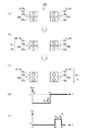
次に、図2に示した抵抗変化型記憶素子のデータ書き込み装置の動作の一例を、図3、図4を参照しながら説明する。詳細には、図3(a)は(RY,RYb)=(R1,R0)の状態を示す概念図、図3(b)は(RY,RYb)=(R0,R1)の状態を示す概念図、図3(c)は図2に示した左側の抵抗変化型記憶素子10Aに流れる電流IWYを示す図、図3(d)は図2に示した右側の抵抗変化型記憶素子10Bに流れる電流IWYbを示す図である。
図3(c)、図3(d)の縦軸において、各抵抗変化型記憶素子の磁化自由層10cから磁化固定層10aの方向へ流れる電流の向きを正とする。
Next, an example of the operation of the data writing device of the resistance change type storage element shown in FIG. 2 will be described with reference to FIGS. 3 and 4. In particular, FIG. 3 (a) (R Y, R Yb) = conceptual diagram showing the state of (R 1, R 0), FIG. 3 (b) (R Y, R Yb) = (
On the vertical axis of FIGS. 3 (c) and 3 (d), the direction of the current flowing from the magnetization
初期状態では、図3(a)に示したように、抵抗変化型記憶素子10A、10Bは、(RY,RYb)=(R1,R0)の状態である。つまり、相補型セル10CはY=1の状態である。
時間T0において、ワードラインWLがハイレベルに設定され、抵抗変化型記憶素子10Aに閾値以上の電流IWYが流れ、抵抗変化型記憶素子10Bに閾値以上の電流IWYbが流れるように、各書込回路21、22が制御を行う。
In the initial state, as shown in FIG. 3 (a), the resistance
At time T0, the wordline WL is set to a high level, the current I WY above the threshold value flows through the resistance change
各抵抗変化型記憶素子には、書込み特性にばらつきがある。
本実施形態では、時間T1において、抵抗変化型記憶素子10Aへの書込みが終了する。詳細には、抵抗変化型記憶素子10Aが、図3(a)に示したRY=R1の状態から、図3(b)に示したRY=R0の状態となる。そして、時間T2において、抵抗変化型記憶素子10Bへの書込みが終了する。詳細には、抵抗変化型記憶素子10Bが、図3(a)に示したRY=R0の状態から、図3(b)に示したRY=R1の状態となる。すなわち、抵抗変化型記憶素子10A、10Bは、(RY,RYb)=(R0,R1)の状態となる。つまり、相補型セル10CはY=0の状態となる。書込み動作が終了した場合、ワードラインWLがLレベルに設定される。
Each resistance change type memory element has variations in writing characteristics.
In the present embodiment, at time T1, writing to the resistance change
次に、相補型セル10CがY=0(初期状態)からY=1となるように書き込む動作を説明する。詳細には、図4(a)は(RY,RYb)=(R1,R0)の状態を示す概念図、図4(b)は(RY,RYb)=(R0,R1)の状態を示す概念図、図4(c)は図2に示した左側の抵抗変化型記憶素子10Aに流れる電流IWYを示す図、図4(d)は図2に示した右側の抵抗変化型記憶素子10Bに流れる電流IWYbを示す図である。
図4(c)、図4(d)の縦軸において、各抵抗変化型記憶素子の磁化自由層10cから磁化固定層10aの方向へ流れる電流の向きを正とする。
初期状態では、図4(a)に示したように、抵抗変化型記憶素子10A、10Bは、(RY,RYb)=(R0,R1)の状態である。
Next, the operation of writing the
On the vertical axis of FIGS. 4 (c) and 4 (d), the direction of the current flowing from the magnetization
In the initial state, as shown in FIG. 4A, the resistance change
時間T0において、ワードラインWLがハイレベルに設定され、抵抗変化型記憶素子10Aに閾値以上の電流IWYが流れ、抵抗変化型記憶素子10Bに閾値以上の電流IWYbが流れるように、各書込回路21、22が制御を行う。
At time T0, the wordline WL is set to a high level, the current I WY above the threshold value flows through the resistance change
本実施形態では、時間T11において、抵抗変化型記憶素子10Bへの書込みが終了する。詳細には、抵抗変化型記憶素子10Bが、図4(a)に示したRY=R1の状態から、図4(b)に示したRY=R0の状態となる。そして、時間T12において、抵抗変化型記憶素子10Aへの書込みが終了する。詳細には、抵抗変化型記憶素子10Aが、図4(a)に示したRY=R0の状態から、図4(b)に示したRY=R1の状態となる。すなわち、抵抗変化型記憶素子10A、10Bは、(RY,RYb)=(R1,R0)の状態となる。つまり、相補型セル10CはY=1の状態となる。
In the present embodiment, at time T11, writing to the resistance change
すなわち、本実施形態では、抵抗変化型記憶素子のデータ書き込み装置は、2つの書込回路21、22を有し、それぞれ相補型セル10Cの各抵抗変化型記憶素子10A、10Bにデータの書込みを行うので、高速に書込み動作を行うことができる。
That is, in the present embodiment, the data writing device of the resistance changing type storage element has two writing
以上、説明したように、本発明の実施形態に係る抵抗変化型記憶素子のデータ書き込み装置は、抵抗変化型記憶素子10A、10Bを備える相補型抵抗変化型記憶素子(相補型セル10C)と、その相補型抵抗変化型記憶素子に抵抗変化を生じさせる書き込み手段(書込回路)と、相補型抵抗変化型記憶素子(相補型セル10C)の書き込み状態を検出する検出手段(検出部30)と、制御手段(制御部40)と、を有する。制御手段(制御部40)は、検出手段(検出部30)の検出信号に基づいて、書き込み手段(書込回路)による書き込み終了を制御する。例えば、検出部30により書込みの終了を検出した場合、制御部40は、書き込み手段(書込回路)による書き込み電流の出力を停止して、書込みを終了する。
As described above, the data writing device of the resistance change type storage element according to the embodiment of the present invention includes a complementary resistance change type storage element (
また、本実施形態に係る抵抗変化型記憶素子のデータ書き込み装置では、書き込み手段(書込回路)は、相補型抵抗変化型記憶素子(相補型セル10C)それぞれの記憶素子(抵抗変化型記憶素子10A、10B)に対応した書込部(書込回路21、22)を備え、書込部(書込回路21、22)により記憶素子(抵抗変化型記憶素子10A、10B)それぞれに同時に逆の抵抗変化を生じさせるように書き込む。制御手段(制御部40)は、検出手段(検出部30)による記憶素子(抵抗変化型記憶素子10A、10B)それぞれの書き込み状態に基づいて、それぞれの記憶素子(抵抗変化型記憶素子10A、10B)の書き込み制御を行う。
すなわち、書込回路21、書込回路22により、相補型セル10Cの抵抗変化型記憶素子10A、10Bそれぞれに同時に書き込むことによって、簡単な構成で、高速に書込み処理を行うことができる。
Further, in the data writing device of the resistance change type storage element according to the present embodiment, the writing means (writing circuit) is the storage element (resistance change type storage element) of each of the complementary resistance change type storage elements (
That is, by simultaneously writing to the resistance change
(第2実施形態:Type2)
図5は、本発明の第2実施形態に係る抵抗変化型記憶素子のデータ書き込み装置の構成例を示す図である。
図5に示した、抵抗変化型記憶素子のデータ書き込み装置では、書き込み手段が、書込回路121と、書込み相補型抵抗変化型記憶素子(10A、10B)それぞれに、順次、逆の抵抗変化を生じさせるように書き込む切り替え手段(切替部122)を有する。詳細には、書込み手段として、書込回路121、及び切替部122を有する。つまり、本実施形態では、書き込み装置は、1つの書込回路121を備え、その書込回路121からの書込み信号を切替部122により、抵抗変化型記憶素子10A、10Bのいずれか一方に書き込んだ後、他方の抵抗変化型記憶素子に書き込む制御を行う。
(Second Embodiment: Type2)
FIG. 5 is a diagram showing a configuration example of a data writing device for a resistance change type storage element according to a second embodiment of the present invention.
In the data writing device of the resistance changing type storage element shown in FIG. 5, the writing means sequentially applies the reverse resistance change to each of the
図5に示したように、書込回路121において、ビットラインBLが切替部122に接続され、ビットラインBLbが抵抗変化型記憶素子10A、及び抵抗変化型記憶素子10Bの磁化固定層10aに電気的に接続されている。
切替部122からのビットラインBL1がNMOSトランジスタ30aのソースに接続され、切替部122からのビットラインBL2がNMOSトランジスタ30bのソースに接続されている。
As shown in FIG. 5, in the
The bit line BL1 from the
NMOSトランジスタ30aのゲート、及びNMOSトランジスタ30bのゲートには、ワードラインWLが接続されている。ワードラインWLは、制御部40に電気的に接続されている。
NMOSトランジスタ30aのドレインは、抵抗変化型記憶素子10Aの磁化自由層10cに電気的に接続されている。NMOSトランジスタ30bのドレインは、抵抗変化型記憶素子10Bの磁化自由層10cに電気的に接続されている。
A word line WL is connected to the gate of the
The drain of the
次に、図5に示した抵抗変化型記憶素子のデータ書き込み装置の動作の一例を、図6、図7を参照しながら説明する。詳細には、図6(a)は(RY,RYb)=(R1,R0)の状態を示す概念図、図6(b)は(RY,RYb)=(R0,R0)の状態を示す概念図、図6(c)は(RY,RYb)=(R0,R1)を示す概念図である。
図6(d)は図5に示した左側の抵抗変化型記憶素子10Aに流れる電流IWYを示す図、図6(e)は図5に示した右側の抵抗変化型記憶素子10Bに流れる電流IWYbを示す図である。図6(d)、図6(e)の縦軸において、各抵抗変化型記憶素子の磁化自由層10cから磁化固定層10aの方向へ流れる電流の向きを正とする。
Next, an example of the operation of the data writing device of the resistance change type storage element shown in FIG. 5 will be described with reference to FIGS. 6 and 7. In particular, FIG. 6 (a) (R Y, R Yb) concept illustrating the state of a = (R 1, R 0), and FIG. 6 (b) (R Y, R Yb) = (
6 (d) is a diagram showing the current I WY flowing through the resistance change
初期状態では、図6(a)に示したように、抵抗変化型記憶素子10A、10Bは、(RY,RYb)=(R1,R0)の状態である。つまり、相補型セル10CはY=1の状態である。
時間T0において、ワードラインWLがハイレベルに設定され、抵抗変化型記憶素子10Aに閾値以上の電流IWYが流れるように、書込回路121、切替部122が制御を行う。
In the initial state, as shown in FIG. 6 (a), the resistance
At time T0, the
時間T31において、抵抗変化型記憶素子10Aが、図6(a)に示したRY=R1の状態から、図6(b)に示したRY=R0の状態となり、抵抗変化型記憶素子10Aへの書込みが終了する(図6(b)の[1]状態、図6(d)の[1]状態)。
各抵抗変化型記憶素子には、書込み特性にばらつきがある。詳細には、各抵抗変化型記憶素子の書込み終了時間にはばらつきがあるので、想定される抵抗変化型記憶素子10Aの最長の書込み終了時間を経過した後、時間T32で、抵抗変化型記憶素子10Bへの書込みを開始する。
At time T31, the resistance change
Each resistance change type memory element has variations in writing characteristics. Specifically, since the write end time of each resistance change type memory element varies, the resistance change type memory element is set at time T32 after the longest write end time of the assumed resistance change
時間T32において、抵抗変化型記憶素子10Bに閾値以上の電流IWYbが流れるように、書込回路121、切替部122が制御を行う。
At time T32, the
時間T33において、抵抗変化型記憶素子10Bへの書込みが終了する。詳細には、抵抗変化型記憶素子10Bが、図6(b)に示したRYb=R0の状態から、図6(c)に示したRYb=R1の状態となる。すなわち、抵抗変化型記憶素子10A、10Bは、(RY,RYb)=(R0,R1)の状態となる(図6(c)の[2]状態、図6(e)の[2]状態)。つまり、相補型セル10CはY=0の状態となる。書込み動作が終了した場合、ワードラインWLがLレベルに設定される。
At time T33, writing to the resistance change
次に、相補型セル10CがY=0(初期状態)からY=1となるように書き込む動作を説明する。詳細には、図7(a)は(RY,RYb)=(R0,R1)の状態を示す概念図、図7(b)は(RY,RYb)=(R1,R1)の状態を示す概念図、図7(c)は(RY,RYb)=(R1,R0)を示す概念図である。
図7(d)は図5に示した左側の抵抗変化型記憶素子10Aに流れる電流IWYを示す図、図7(e)は図5に示した右側の抵抗変化型記憶素子10Bに流れる電流IWYbを示す図である。図7(d)、図7(e)の縦軸において、各抵抗変化型記憶素子の磁化自由層10cから磁化固定層10aの方向へ流れる電流の向きを正とする。
Next, the operation of writing the
FIG. 7 (d) is a diagram showing the current I WY flowing through the resistance change
時間T0において、ワードラインWLがハイレベルに設定され、抵抗変化型記憶素子10Aに閾値以上の電流IWYが流れるように、書込回路121、切替部122が制御を行う。
At time T0, the
時間T41において、抵抗変化型記憶素子10Aが、図7(a)に示したRY=R0の状態から、図7(b)に示したRY=R1の状態となり、抵抗変化型記憶素子10Aへの書込みが終了する(図7(b)の[3]状態、図7(d)の[3]状態)。各抵抗変化型記憶素子の書込み終了時間にはばらつきがあるので、想定される抵抗変化型記憶素子10Aの最長の書込み終了時間を経過した後、時間T42で、抵抗変化型記憶素子10Bへの書込みを開始する。
At time T41, the resistance change
時間T42において、抵抗変化型記憶素子10Bに閾値以上の電流IWYbが流れるように、書込回路121、切替部122が制御を行う。
At time T42, the
時間T43において、抵抗変化型記憶素子10Bへの書込みが終了する。詳細には、抵抗変化型記憶素子10Bが、図7(b)に示したRY=R1の状態から、図7(c)に示したRY=R0の状態となる。すなわち、抵抗変化型記憶素子10A、10Bは、(RY,RYb)=(R1,R0)の状態となる(図7(c)の[4]状態、図7(e)の[4]状態)。つまり、相補型セル10CはY=1の状態となる。書込み動作が終了した場合、ワードラインWLがLレベルに設定される。
At time T43, writing to the resistance change
以上、説明したように、本発明の第2実施形態に係る抵抗変化型記憶素子のデータ書き込み装置は、抵抗変化型記憶素子10A、10Bを備える相補型抵抗変化型記憶素子(相補型セル10C)と、その相補型抵抗変化型記憶素子に抵抗変化を生じさせる書き込み手段(書込回路121)と、相補型抵抗変化型記憶素子(相補型セル10C)の書き込み状態を検出する検出手段(検出部30)と、検出手段(検出部30)の検出信号に基づいて、書き込み手段(書込回路121)の書き込み終了を制御する制御手段(制御部40)と、を有する。
書き込み手段(書込回路121)は、相補型抵抗変化型記憶素子(相補型セル10C)の抵抗変化型記憶素子10A、10Bそれぞれに、順次、逆の抵抗変化を生じさせるように書き込む切り替え手段(切替部122)を備える。
すなわち、第2実施形態の抵抗変化型記憶素子のデータ書き込み装置では、切替部122により、書込み対象を、相補型セル10Cの抵抗変化型記憶素子10A、10Bの一方、又は他方に切り替えながら、書込みを行うことができるので、書込回路を一つの回路構成とすることができ、第1実施形態の2つの書込回路を備えたデータ書き込み装置と比較して、トランジスタなどの構成要素を少なくすることができ、全体の回路規模を小さくすることができる。
As described above, the data writing device of the resistance changing type storage element according to the second embodiment of the present invention is a complementary resistance changing type storage element (
The writing means (writing circuit 121) is a switching means (writing circuit 121) for writing to each of the resistance changing
That is, in the data writing device of the resistance changing type storage element of the second embodiment, the
(第3実施形態:Type3)
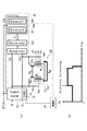
図8は本発明の第3実施形態に係る抵抗変化型記憶素子のデータ書き込み装置を説明するための図である。詳細には、図8(a)は抵抗変化型記憶素子のデータ書き込み装置の構成例を示す概念図である。図8(b)は図8(a)に示した抵抗変化型記憶素子のデータ書き込み装置の動作の一例を示すタイミングチャートである。
図8(a)に示した、データ書込み装置は、相補型セル10C、書込回路20、検出部30、及び制御部40を有する。
(Third Embodiment: Type3)
FIG. 8 is a diagram for explaining a data writing device of the resistance change type storage element according to the third embodiment of the present invention. In detail, FIG. 8A is a conceptual diagram showing a configuration example of a data writing device for a resistance change type storage element. FIG. 8B is a timing chart showing an example of the operation of the data writing device of the resistance change type storage element shown in FIG. 8A.
The data writing device shown in FIG. 8A includes a
相補型セル10Cは、2つの抵抗変化型記憶素子10A、抵抗変化型記憶素子10Bを有する。抵抗変化型記憶素子10Aの記憶状態をYで示し、抵抗変化型記憶素子10Bの記憶状態をYbで示している。
The
書込回路20には、書込みデータ信号Aが入力される。また、書込回路20には、書込み用信号WCK(書込み用クロック)が入力される。
The write data signal A is input to the
書込回路20と相補型セル10Cは、ビットラインBL、ビットラインBLb、ワードラインWLにより電気的に接続されている。詳細には、ビットラインBLがNMOSトランジスタ30aのソースに電気的に接続され、NMOSトランジスタ30aのドレインが抵抗変化型記憶素子10Aの磁化自由層10c側に電気的に接続されている。
ビットラインBLbがNMOSトランジスタ30bのソースに電気的に接続され、NMOSトランジスタ30bのドレインが抵抗変化型記憶素子10Bの磁化自由層10c側に電気的に接続されている。
ワードライン(WL)が、NMOSトランジスタ30aのソース、及びNMOSトランジスタ30bのソースに電気的に接続されている。
The
The bit line BLb is electrically connected to the source of the
The word line (WL) is electrically connected to the source of the
また、本実施形態では、書込回路20は、相補型抵抗変化型素子(相補型セル10C)の直列接続された抵抗変化型記憶素子(10A、10B)に電流を流し、その電流の流れる方向を切り替える切り替え手段(切替部50)を有する。
Further, in the present embodiment, the writing
検出部30は、相補型抵抗変化型記憶素子(相補型セル10C)の書き込み状態(書込回路20)を検出する。詳細には、検出部30は、ビットラインBLの電圧、ビットラインBLbの電圧を検出し、検出信号を制御部40へ出力する。
The
制御部40は、検出手段(検出部30)の検出信号に基づいて、書き込み手段(書込回路20)の書き込み終了を制御する。
The
図8(a)に示した例の抵抗変化型記憶素子のデータ書き込み装置の動作の一例を説明する。先ず、データAが‘0’の場合の書込み動作を説明する。初期状態では、(Y,Yb)=(1,0)となっている。
時間T51において、書込み用クロック信号WCKがHレベル(WCK=1)に設定され、書込回路20は書込みモードに設定される。ワードラインWLがHレベルに設定される。ビットラインBLからビットラインBLbの方向に電流が流れるように設定される。このとき、ビットラインBL側の電圧変化をモニタする。
An example of the operation of the data writing device of the resistance change type storage element of the example shown in FIG. 8A will be described. First, the writing operation when the data A is '0' will be described. In the initial state, (Y, Yb) = (1,0).
At time T51, the write clock signal WCK is set to H level (WCK = 1) and the
時間T52において、先ず、Y=0が左側の抵抗変化型記憶素子10A(MTJ素子)に書き込まれ、(Y,Yb)=(0,0)となる。書き込みパスの抵抗値が減少し、抵抗変化型記憶素子10Aの磁化固定層側から抵抗変化型記憶素子10Bの磁化固定層側への電流IWは増加する。そして、ビットラインBLの電圧が、VHからVLに遷移する(VH>VL)。
At time T52, first, Y = 0 is written in the resistance change
時間T53において、右側の抵抗変化型記憶素子10B(MTJ素子)に記憶状態Y=1が書き込まれて、(Y,Yb)=(0,1)となる。書き込みパスの抵抗値が増加し、IWは減少する。また、ビットラインBLの電圧がVLからVHに遷移する。そして、時間T52、及び時間T53における2回の書込み終了検出によって、ワードラインWLがLレベル(WL=0)となり、書き込み動作が停止する。
At time T53, the storage state Y = 1 is written to the resistance change
次に、データAが‘1’の場合の書込み動作を説明する。初期状態では、(Y,Yb)=(0,1)となっている。尚、タイミングチャートは省略する。 Next, the writing operation when the data A is '1' will be described. In the initial state, (Y, Yb) = (0,1). The timing chart is omitted.
時間T51において、書込み用クロック信号WCKがHレベル(WCK=1)に設定され、書込回路20は書込みモードに設定される。ワードラインWLがHレベルに設定される。ビットラインBLbからビットラインBLの方向に電流が流れるように設定される。このとき、ビットラインBLb側の電圧変化をモニタする。
At time T51, the write clock signal WCK is set to H level (WCK = 1) and the
時間T52において、Y=0が右側の抵抗変化型記憶素子10B(MTJ素子)に書き込まれ、(Y,Yb)=(0,0)となる。書き込みパスの抵抗値が減少し、抵抗変化型記憶素子10Aの磁化固定層側から抵抗変化型記憶素子10Bの磁化固定層側への電流IWは増加する。そして、ビットラインBLbの電圧がVHからVLに遷移する(VH>VL)。
At time T52, Y = 0 is written to the resistance change
時間T53において、左側の抵抗変化型記憶素子10A(MTJ素子)に記憶状態Y=1が書き込まれ、(Y,Yb)=(1,0)となる。このとき、書き込みパスの抵抗値が増加し、IWは減少する。また、ビットラインBLbの電圧がVLからVHに遷移する。そして、時間T52、及び時間T53における2回の書込み終了検出によって、ワードラインWLがLレベル(WL=0)となり、書き込み動作が停止する。
At time T53, the storage state Y = 1 is written to the resistance change
次に、図8に示した実施形態の一実施例に係る抵抗変化型記憶素子のデータ書き込み装置について、図9〜図12を参照しながら説明する。 Next, the data writing device of the resistance change type storage element according to the embodiment of the embodiment shown in FIG. 8 will be described with reference to FIGS. 9 to 12.
図9(a)に示したように、本実施例の抵抗変化型記憶素子のデータ書き込み装置は、出力端を境にして、A部分(Part A)とB部分(Part B)に分けられる。データ書き込み装置は、A部分(Part A)として、PMOSトランジスタ9a(Mp)を有し、B部分(Part B)として、相補型セル10C、及びNMOSトランジスタ9b(MN)を有する。つまり、A部分(Part A)は、PMOSトランジスタ9aに相応する部分であり負荷抵抗となる。
なお、図9(a)では、データ書き込み装置において、A部分(PartA)としてビットラインBLの電圧を検出する構成を示し、B部分(PartB)としてビットラインBLbを接地する構成のみを示し、A部分(PartA)としてビットラインBLbの電圧を検出する構成、及びB部分(PartB)としてビットラインBLを接地する構成は省略して示している。
以下、図9(a)に示した、ビットラインBLの電圧VBLを検出する構成について説明する。
As shown in FIG. 9A, the data writing device of the resistance change type storage element of this embodiment is divided into an A portion (Part A) and a B portion (Part B) with the output end as a boundary. The data writing device has a
Note that FIG. 9A shows a configuration in which the voltage of the bit line BL is detected as the A portion (Part A) in the data writing device, and only the configuration in which the bit line BLb is grounded as the B portion (Part B) is shown. The configuration in which the voltage of the bit line BLb is detected as a part (Part A) and the configuration in which the bit line BL is grounded as the B portion (Part B) are omitted.
Hereinafter, the configuration for detecting the voltage VBL of the bit line BL shown in FIG. 9A will be described.
PMOSトランジスタ9a(Mp)は、ソースが電源電圧VDDに接続され、ドレインがビットラインBLを介して相補型セル10Cに電気的に接続されている。また、トランジスタ9aと相補型セル10Cの間の接続ノードは、電圧VBLを出力する出力端であり、検出部30(図8を参照)に接続されている。PMOSトランジスタ9a(Mp)の制御ゲートは、制御部の制御により必要に応じて基準電圧(0V)に接続される。
The source of the
NMOSトランジスタ9b(MN)は、ソースがビットラインBLbを介して相補型セル10Cに接続され、ドレインが基準電圧GND(0V)に接地されている。NMOSトランジスタ9b(MN)の制御ゲートは、制御部の制御により、必要に応じて電源電圧VDDに接続される。
The source of the
相補型セル10Cは、2つの抵抗変化型記憶素子10A、抵抗変化型記憶素子10Bを有する。抵抗変化型記憶素子10A、10Bは、上述したように、磁化固定層10aと、磁化自由層10cの間にトンネルバリア層10bが設けられている。ビットラインBLがNMOSトランジスタ30aのソースに電気的に接続され、NMOSトランジスタ30aのドレインが抵抗変化型記憶素子10Aの磁化自由層10c側に電気的に接続されている。ビットラインBLbがNMOSトランジスタ30bのソースに電気的に接続され、NMOSトランジスタ30bのドレインが抵抗変化型記憶素子10Bの磁化自由層10c側に電気的に接続されている。NMOSトランジスタ30a、30bの制御ソースは、ワードラインWLに接続されている。
The
図9(b)は図9(a)に示した抵抗変化型記憶素子のデータ書き込み装置の負荷特性曲線、及び電圧−電流特性曲線を示している。図9(a)に示した、A部分(Part A)とB部分(Part B)には共通する電流Iwが流れるため、VBLの出力端の電圧は、A部分(Part A)の負荷特性の曲線とB部分(Part B)の電圧−電流特性曲線とが交差する交点の電圧となる。詳細には、図9(b)は、A部分(Part A)の負荷特性の曲線、及びB部分(Part B)の電圧−電流特性曲線を示している。
B部分(Part B)の電圧−電流特性曲線は、書き込みされた相補型セル10Cの抵抗変化型記憶素子10A、10Bの記憶状態がそれぞれ(Y=0、Yb=0)の場合(低抵抗)と、(Y=1、Yb=0)、又は(Y=0、Yb=1)の場合(高抵抗)を示している。
FIG. 9B shows a load characteristic curve and a voltage-current characteristic curve of the data writing device of the resistance change type storage element shown in FIG. 9A. Since a common current I w flows through the A part (Part A) and the B part (Part B) shown in FIG. 9A, the voltage at the output end of the V BL is the load of the A part (Part A). It is the voltage at the intersection where the characteristic curve and the voltage-current characteristic curve of the B part (Part B) intersect. In detail, FIG. 9B shows a curve of the load characteristic of the A portion (Part A) and a voltage-current characteristic curve of the B portion (Part B).
The voltage-current characteristic curve of the B part (Part B) shows the case where the storage states of the resistance change
相補型セル10Cの抵抗変化型記憶素子10A、10Bの記憶状態がそれぞれ(Y=0、Yb=0)の場合(低抵抗)、VBLの出力端の電圧は、A部分(Part A)の負荷特性の曲線とB部分(Part B)の電圧−電流特性曲線とが交差する交点の電圧VLとなる。A部分(Part A)とB部分(Part B)に流れる電流Iwは電流値IW1aである。この電流値IW1aは、抵抗変化型記憶素子が低抵抗状態(RY=R0)から高抵抗状態(RY=R1)に遷移するのに必要な電流閾値(Iw1)以上の電流Iw1+Iαに設定されている。Iαは僅かな電流値。
When the storage states of the resistance-changing
相補型セル10Cの抵抗変化型記憶素子10A、10Bの記憶状態がそれぞれ(Y=1、Yb=0)、又は(Y=0、Yb=1)の場合(高抵抗)、VBLの出力端の電圧は、A部分(Part A)の負荷特性の曲線とB部分(Part B)の電圧−電流特性曲線とが交差する交点の電圧VHとなる。A部分(Part A)とB部分(Part B)に流れる電流Iwは電流値IW0aである。この電流値IW0aは、抵抗変化型記憶素子が高抵抗状態(RY=R1)から低抵抗状態(RY=R0)に遷移するのに必要な電流閾値(Iw0)以上の電流Iw0+Iβに設定されている。Iβは僅かな電流値。IβはIαと同じ電流値であってもよいし、異なる電流値であってもよい。
When the storage states of the resistance-changing
検出部は、接続ノードの電圧VBLが、電圧VHであるか、電圧VLであるかにより、抵抗変化型記憶素子10A、10Bの書き込み状態を判別することができる。
The detection unit can determine the writing state of the resistance change
図10は図9に示した抵抗変化型記憶素子のデータ書き込み装置の書込み動作時の電圧VBLの一例を示す図である。検出部30(図8を参照)は、センスアンプを有し、接続ノードの電圧VBLを検出している。
時間T0において、電圧VBLが予め規定された閾値VTH以上の電圧値である場合、相補型セル10Cの抵抗変化型記憶素子の記憶状態が(Y=1、Yb=0)、又は(Y=0、Yb=1)と検出する。
1stスイッチングのタイミングとしての時間T61において、電圧VBLが閾値VTH以上の電圧値から、閾値VTH未満の電圧値に変化した場合、相補型セル10Cの抵抗変化型記憶素子の記憶状態が(Y=0、Yb=0)となったことを検出する。
FIG. 10 is a diagram showing an example of the voltage V BL during the writing operation of the data writing device of the resistance change type storage element shown in FIG. The detection unit 30 (see FIG. 8) has a sense amplifier and detects the voltage V BL of the connection node.
When the voltage V BL is a voltage value equal to or higher than a predetermined threshold value V TH at time T0, the storage state of the resistance change type storage element of the
At time T61 as timing of 1st switching, the voltage V BL threshold V TH above voltage value, when the change in the voltage value less than the threshold V TH, the memory state of the resistance variable memory element of the
2ndスイッチングのタイミングとしての時間T62において、電圧VBLが閾値VTH未満の電圧値から、閾値VTH以上の電圧値に変化した場合、相補型セル10Cの抵抗変化型記憶素子の記憶状態が(Y=1、Yb=0)、又は(Y=0、Yb=1)となったことを検出する。
At time T62 as timing 2nd switching, the voltage value lower than the voltage V BL threshold V TH, if changed to the threshold V TH above voltage value, the storage state of the resistance variable memory element of the
次に、図9に示した抵抗変化型記憶素子のデータ書き込み装置の動作の一例を、図11、図12などを参照しながら説明する。
図11は図9に示したデータ書き込み装置が相補型セル10CにY=0を書き込む動作の一例を示す図である。詳細には、図11(a)は相補型セルの記憶状態が(RY,RYb)=(R1,R0)の場合を示す図、図11(b)は相補型セルの記憶状態が(RY,RYb)=(R0,R0)の場合を示す図、図11(c)は相補型セルの記憶状態が(RY,RYb)=(R0,R1)の場合を示す図である。
図11(d)はデータ書き込み装置の負荷特性曲線、及び電圧−電流特性曲線を示す図、図11(e)は抵抗変化型記憶素子の抵抗−電圧特性の一例を示す図、図11(f)はデータ書き込み装置の相補型セルに流れる電流の一例を示す図である。
Next, an example of the operation of the data writing device of the resistance change type storage element shown in FIG. 9 will be described with reference to FIGS. 11 and 12.
FIG. 11 is a diagram showing an example of an operation in which the data writing device shown in FIG. 9 writes Y = 0 to the
FIG. 11 (d) is a diagram showing a load characteristic curve and a voltage-current characteristic curve of a data writing device, and FIG. 11 (e) is a diagram showing an example of resistance-voltage characteristics of a resistance change type storage element, FIG. 11 (f). ) Is a diagram showing an example of the current flowing through the complementary cell of the data writing device.
図11(a)に示したように、初期状態では、相補型セル10Cの記憶状態が(RY,RYb)=(R1,R0)となっている(Y=1)。相補型セル10Cの抵抗値はR1+R0である。
As shown in FIG. 11 (a), in the initial state, the storage state of the
時間T0において、書込回路は、ビットライン電圧VBLをVHに設定して、相補型セル10Cに電流Iw0aが流れる。
At time T0, the write circuit sets the bitline voltage V BL to V H and a current I w0a flows through the
時間T61において、図11(b)に示すように、抵抗変化型記憶素子10Aの磁化自由層の磁化の向きが反転し、低抵抗状態RY=R0となり(図11(e)の[1]状態から[2]状態へ遷移)、相補型セル10Cが(RY,RYb)=(R0,R0)となり、相補型セル10Cの抵抗値がR0+R0となり、ビットライン電圧VBLがVLとなり、電流Iw1aが流れる(図11(f)の[A]状態、図11(d)の[A]状態)。
At time T61, as shown in FIG. 11B, the direction of magnetization of the magnetization free layer of the resistance change
時間T62において、図11(c)に示すように、抵抗変化型記憶素子10Bの磁化自由層の磁化の向きが反転し、高抵抗状態RYb=R1となり(図11(e)の[3]状態)、相補型セル10Cが(RY,RYb)=(R0,R1)となり、相補型セル10Cの抵抗値がR0+R1となり、ビットライン電圧VBLがVHとなり、電流Iw0aが流れる(図11(f)の[B]状態、図11(d)の[B]状態)。
At time T62, as shown in FIG. 11 (c), the direction of magnetization of the magnetization free layer of the resistance change
時間T63において、書込み動作が終了すると、ワードラインWLがLレベルとなり、図11(f)に示すように、電流IWが0となる。 When the writing operation is completed at the time T63, the word line WL becomes the L level, and the current I W becomes 0 as shown in FIG. 11 (f).
図12は図9に示したデータ書き込み装置が相補型セル10CにY=1を書き込む動作の一例を示す図である。詳細には、図12(a)は相補型セルの記憶状態が(RY,RYb)=(R0,R1)の場合を示す図、図12(b)は相補型セルの記憶状態が(RY,RYb)=(R0,R0)の場合を示す図、図12(c)は相補型セルの記憶状態が(RY,RYb)=(R1,R0)の場合を示す図である。
図12(d)はデータ書き込み装置の負荷特性曲線、及び電圧−電流特性曲線を示す図、図12(e)は抵抗変化型記憶素子の抵抗−電圧特性の一例を示す図、図12(f)はデータ書き込み装置の相補型セルに流れる電流の一例を示す図である。
なお、図12は、図9(a)に示していないビットラインBLbの電圧を検出する構成の書き込み動作を示している。
FIG. 12 is a diagram showing an example of an operation in which the data writing device shown in FIG. 9 writes Y = 1 to the
FIG. 12 (d) is a diagram showing a load characteristic curve and a voltage-current characteristic curve of a data writing device, and FIG. 12 (e) is a diagram showing an example of resistance-voltage characteristics of a resistance change type storage element, FIG. 12 (f). ) Is a diagram showing an example of the current flowing through the complementary cell of the data writing device.
Note that FIG. 12 shows a writing operation having a configuration for detecting the voltage of the bit line BLb not shown in FIG. 9A.
図12(a)に示したように、初期状態では、相補型セル10Cの記憶状態が(RY,RYb)=(R0,R1)となっている(Y=0)。相補型セル10Cの抵抗値はR0+R1である。相補型セル10CにY=1を書き込む場合、抵抗変化型記憶素子10Bから抵抗変化型記憶素子10Aへ電流を流す。
As shown in FIG. 12A, in the initial state, the storage state of the
時間T0において、書込回路は、ビットライン電圧VBLbをVHに設定して、相補型セル10Cに電流Iw0aが流れる。
At time T0, the write circuit sets the bitline voltage V BLb to V H and a current I w0a flows through the
時間T71において、図12(b)に示すように、抵抗変化型記憶素子10Bの磁化自由層の磁化の向きが反転し、低抵抗状態RYb=R0となり(図12(e)の[4]状態から[7]状態へ遷移)、抵抗変化型記憶素子10Aは低抵抗状態RY=R0であり(図12(b)の[5]状態、図12(e)の[5]状態)、相補型セル10Cが(RY,RYb)=(R0,R0)となり、相補型セル10Cの抵抗値がR0+R0となり、ビットライン電圧VBLbがVLとなり、電流Iw1aが流れる(図12(f)の[C]状態、図12(d)の[C]状態)。
At time T71, as shown in FIG. 12B, the direction of magnetization of the magnetization free layer of the resistance change
時間T72において、図12(c)に示すように、抵抗変化型記憶素子10Aの磁化自由層の磁化の向きが反転し、高抵抗状態RY=R1となり(図12(e)の[6]状態)、相補型セル10Cが(RY,RYb)=(R1,R0)となり、相補型セル10Cの抵抗値がR1+R0となり、ビットライン電圧VBLbがVHとなり、電流Iw0aが流れる(図12(f)の[D]状態、図12(d)の[D]状態)。
At time T72, as shown in FIG. 12 (c), the direction of magnetization of the magnetization free layer of the resistance change
時間T73において、書込み動作が終了すると、ワードラインWLがLレベルとなり、図12(f)に示すように、電流IWが0となる。 When the writing operation is completed at the time T73, the word line WL becomes the L level, and the current I W becomes 0 as shown in FIG. 12 (f).
図13は、図8に示した実施形態の一実施例に係る抵抗変化型記憶素子のデータ書き込み装置を説明するための図である。詳細には、図13(a)はデータ書き込み装置の一例を示す図、図13(b)は電流Iwのタイミングチャートである。図13(b)において、縦軸に電流Iwの絶対値を示し、横軸に時間(Time)を示す。図13(b)は、図11(f)、及び図12(f)と同じであるので、説明を省略する。 FIG. 13 is a diagram for explaining a data writing device of the resistance change type storage element according to the embodiment of the embodiment shown in FIG. In detail, FIG. 13A is a diagram showing an example of a data writing device, and FIG. 13B is a timing chart of a current I w . In FIG. 13B, the vertical axis shows the absolute value of the current I w , and the horizontal axis shows the time (Time). Since FIG. 13 (b) is the same as FIG. 11 (f) and FIG. 12 (f), the description thereof will be omitted.
図13に示した抵抗変化型記憶素子のデータ書き込み装置は、書き込み手段としての書込回路20、相補型セル10C、検出部30、及び制御部40を有する。
本実施形態では、書込回路20は、書込み駆動源25、切替部50(切り替え手段)を有する。
書込み駆動源25(カレントソース)は、相補型セル10Cの抵抗変化型記憶素子10A、10Bへ書き込むための電流源である。
切替部50(切り替え手段)は、相補型抵抗変化型記憶素子の直列接続された記憶素子に電流を流し、電流の流れる方向を切り替える。
The data writing device of the resistance change type storage element shown in FIG. 13 includes a
In the present embodiment, the writing
The write drive source 25 (current source) is a current source for writing to the resistance change
The switching unit 50 (switching means) passes a current through the storage elements connected in series of the complementary resistance change type storage elements, and switches the direction in which the current flows.
検出部30は、書込み駆動源25と直列接続された記憶素子(抵抗変化型記憶素子10A、10B)間の電位変化を検出する。
また、検出部30は、相補型抵抗変化型記憶素子(相補型セル10C)の一方の記憶素子(抵抗変化型記憶素子)の記憶状態の変化と、他方の記憶素子(抵抗変化型記憶素子)の記憶状態の変化を検出する。
制御部40は、検出部30による記憶素子それぞれの書き込み状態に基づいて、それぞれの記憶素子の書き込み制御を行う。
The
Further, the
The
また、本実施形態では、検出手段としての検出部30は、マルチプレクサ311(選択回路)、センスアンプ312、検出装置320を有する。
Further, in the present embodiment, the
マルチプレクサ311は、相補型セル10Cの抵抗変化型記憶素子10A、10Bのいずれかの抵抗変化を示す電圧信号を切替えて出力する。
The
センスアンプ312は、マルチプレクサ311から出力した信号の電圧を増幅し、電圧信号Vsとして検出装置320に出力する。
The
検出装置320は、相補型抵抗変化型記憶素子(相補型セル10C)の一方の記憶素子(抵抗変化型記憶素子)の抵抗変化を検出する第1の検出手段(第1検出部321)と、相補型抵抗変化型記憶素子(相補型セル10C)の他方の記憶素子(抵抗変化型記憶素子)の抵抗変化を検出する第2の検出手段(第2検出部322)と、を有する。
第1検出部321は、抵抗変化型記憶素子10A、10Bのいずれか一方への書込みの終了を1回目の電圧変化で検知し、第2検出部322は他方の抵抗変化型記憶素子への書込み終了を2回目の電圧変化で検知し、検知信号を出力する。
The
The
書込回路20には、書込みデータ信号A、書込みデータ信号Ab(反転)が入力される。書込み用クロック信号WCKが、書込回路20、及び検出装置320に入力するための信号線が書込回路20、及び検出装置320に設けられている。
A write data signal A and a write data signal Ab (inverted) are input to the
また、書込み駆動源25(カレントソース)とマルチプレクサ311には、ビットラインBL、BLbが電気的に接続され、ビットラインBL、BLbがトランジスタ30a、30bのソースに接続されている。
また、本実施形態では、検出装置320から書込みエンド信号などの検出信号ENが、書込回路20へ出力されるように構成されている。
Further, the bit lines BL and BLb are electrically connected to the write drive source 25 (current source) and the
Further, in the present embodiment, the
次に、図14を参照しながら、図13に示した抵抗変化型記憶素子のデータ書き込み装置の書込み駆動源25(Current Source)の構成例を説明する。 Next, a configuration example of a write drive source 25 (Current Source) of the data writing device of the resistance change type storage element shown in FIG. 13 will be described with reference to FIG.
書込み駆動源25は、NAND回路25a、NOR回路25b、NOR回路25c、PMOSトランジスタ25d、NMOSトランジスタ25e、PMOSトランジスタ25f、NMOSトランジスタ25gを有する。
The
NAND回路25aには、クロック信号を有効化するイネーブル信号ENと、書込み用クロック信号WCKが入力される。なお、イネーブル信号ENは、検出装置からの書込み終了を示すエンド信号であり、前回の書込み動作が終了し、次回の書込み動作を許容することを示している。以下では、イネーブル信号ENを検出信号ENで表記する。
NAND回路25aは、検出信号ENと書込み用クロック信号WCKが共に“Low”のとき、及び検出信号ENと書込み用クロック信号WCKの何れか一方が“Low”で他方が“High”のときに“High”を出力し、検出信号ENと書込み用クロック信号WCKが共に“High”のときは“Low”を出力する。
An enable signal EN for validating the clock signal and a write clock signal WCK are input to the
In the
NOR回路25bには、NAND回路25aからの出力と、書込みデータ信号Ab(反転)とが入力される。NOR回路25cには、NAND回路25aからの出力と、書込みデータ信号Aとが入力される。
The output from the
PMOSトランジスタ25dのソースが電源電圧VDDに接続され、ドレインがビットラインBLに接続され、ゲートはNOR回路25cの出力端に接続されている。
NMOSトランジスタ25eのソースがビットラインBLに接続され、ドレインが接地され、ゲートがNOR回路25cの出力端に接続されている。
The source of the
The source of the
PMOSトランジスタ25fのソースが電源電圧VDDに接続され、ドレインがビットラインBLbに接続され、ゲートはNOR回路25bの出力端に接続されている。
NMOSトランジスタ25gのソースがビットラインBLbに接続され、ドレインが接地され、ゲートがNOR回路25bの出力端に接続されている。
The source of the
The source of the
図15は、図13に示した抵抗変化型記憶素子のデータ書き込み装置のマルチプレクサ311とセンスアンプ312の構成例を示す図である。
FIG. 15 is a diagram showing a configuration example of a
マルチプレクサ311は、PMOSトランジスタ311a、NMOSトランジスタ311b、PMOSトランジスタ311c、NMOSトランジスタ311dを有する。
PMOSトランジスタ311aのゲートには書込みデータ信号Aが入力され、ソースがビットラインBLに接続され、ドレインがセンスアンプ312に接続されている。
NMOSトランジスタ311bのソースにはビットラインBLが接続され、ドレインがセンスアンプ312に接続され、ゲートには書込みデータ信号Ab(反転)が入力される。
PMOSトランジスタ311cのソースにはビットラインBLbが接続され、ドレインがセンスアンプ312に接続され、ゲートには書込みデータ信号Abが入力される。
NMOSトランジスタ311dのソースにはビットラインBLbが接続され、ゲートには書込みデータ信号Aが入力され、ドレインがセンスアンプ312に接続されている。
The
A write data signal A is input to the gate of the
A bit line BL is connected to the source of the
A bit line BLb is connected to the source of the
A bit line BLb is connected to the source of the
すなわち、書込みデータ信号AがL状態のとき、ビットラインBLの電圧がセンスアンプに出力され、書込みデータ信号AがH状態のとき、ビットラインBLbの電圧がセンスアンプに出力される。 That is, when the write data signal A is in the L state, the voltage of the bit line BL is output to the sense amplifier, and when the write data signal A is in the H state, the voltage of the bit line BLb is output to the sense amplifier.
センスアンプ312は、PMOSトランジスタ312a、NMOSトランジスタ312b、PMOSトランジスタ312c、NMOSトランジスタ312dを有する。
PMOSトランジスタ312aのソースは電源電圧VDDに接続され、ゲートはマルチプレクサの出力端に接続され、ドレインが次段のトランジスタ312c、312dのゲートに接続されている。
NMOSトランジスタ312bのドレインは接地され、ゲートはマルチプレクサの出力端に接続され、ドレインが次段のトランジスタ312c、312dのゲートに接続されている。
PMOSトランジスタ312cのソースは電源電圧VDDに接続され、ゲートは前段のPMOSトランジスタ312aのドレイン、及びトランジスタ312bのソースに接続され、ドレインは信号Sを出力する出力端に接続されている。
NMOSトランジスタ312dのドレインは接地され、ゲートは前段のPMOSトランジスタ312aのドレイン、及びトランジスタ312bのソースに接続され、ソースは信号Sを出力する出力端に接続されている。
つまり、センスアンプ312は、入力信号を反転増幅して出力する。
The
The source of the
The drain of the
The source of the MOSFET transistor 312c is connected to the power supply voltage V DD , the gate is connected to the drain of the
The drain of the
That is, the
図16(a)は、図13に示した抵抗変化型記憶素子のデータ書き込み装置の第1検出部321(Detector0)、第2検出部(Detector1)の構成例を示す図である。図16(b)は図16(a)の第1検出部321、第2検出部322の動作の一例を示すタイミングチャートである。
FIG. 16A is a diagram showing a configuration example of a first detection unit 321 (Detector0) and a second detection unit (Detector1) of the data writing device of the resistance change type storage element shown in FIG. FIG. 16B is a timing chart showing an example of the operation of the
第1検出部321は、PMOSトランジスタ321a、NMOSトランジスタ321b、PMOSトランジスタ321c(MP0)、NMOSトランジスタ321d(MN0)、及びNMOSトランジスタ321e(MN1)を有する。
PMOSトランジスタ321aのゲートには、センスアンプからの信号Sが入力され、ソースが電源電圧VDDに接続され、ドレインがNMOSトランジスタ321dのゲート、ノードN0、及びNMOSトランジスタ321bのソースに接続されている。NMOSトランジスタ321bのゲートには、センスアンプからの信号Sが入力され、ソースがPMOSトランジスタ321aのドレインに接続され、ドレインが接地されている(GND(0V))。
PMOSトランジスタ321c(MP0)のゲートには、書込み用クロック信号WCKが入力され、ソースが電源電圧VDDに接続され、ドレインがノードN1、及び第2検出部322の入力端に接続されている。NMOSトランジスタ321d(MN0)のゲートはノードN0に接続され、ソースがノードN1に接続され、ドレインがNMOSトランジスタ321eのソースに接続されている。NMOSトランジスタ321e(MN1)のゲートには書込み用クロック信号WCKが入力され、ドレインが接地され、ソースがNMOSトランジスタ321dのドレインに接続されている。
The
The signal S from the sense amplifier is input to the gate of the
A writing clock signal WCK is input to the gate of the
第2検出部322は、PMOSトランジスタ322a、NMOSTトランジスタ322b、PMOSトランジスタ322c(MP1)、NMOSトランジスタ322d(MN2)、及びNMOSトランジスタ322e(MN3)を有する。
The
PMOSトランジスタ322aのゲートは、第1検出部の出力端であるノードN1に接続され、ソースが電源電圧VDDに接続され、ドレインがノードN2に接続されている。NMOSTトランジスタ322bのゲートは、第1検出部の出力端であるノードN1に接続され、ソースがノードN2に接続され、ドレインが接地されている(GND(0V))。
PMOSトランジスタ322c(MP1)のゲートはノードN2に接続され、ソースが電源電圧VDDに接続され、ドレインが出力端に接続されている。出力端からは、検出信号ENが出力される。NMOSトランジスタ322d(MN2)のゲートには、センスアンプからの信号Sが入力され、ソースが出力端に接続され、ドレインがNMOSトランジスタ322e(MN3)のソースに接続されている。NMOSトランジスタ322e(MN3)のゲートはノードN2に接続され、ソースがNMOSトランジスタ322d(MN2)のドレインに接続され、ドレインが接地されている(GND(0V))。
The gate of the
The gate of the
次に、第1検出部321と第2検出部322の動作の一例を説明する。
図16(b)に示したように、初期状態では、書込み用クロック信号WCKがLレベル、信号SがHレベル、ノードN0がLレベル、ノードN1がLレベル、ノードN2がLレベル、検出信号ENがHレベルとなっている。検出信号ENはHレベルとなっているが、書き込み電流は流れない。
Next, an example of the operation of the
As shown in FIG. 16B, in the initial state, the write clock signal WCK is L level, the signal S is H level, the node N0 is L level, the node N1 is L level, the node N2 is L level, and the detection signal. EN is at H level. The detection signal EN is at H level, but no write current flows.
時間T91において、書込み用クロック信号WCKがHレベルに設定され、書き込み開始、及びモニタを開始する。PMOSトランジスタ321c(MP0)とNMOSトランジスタ321d(MN0)はオフ状態となり、ノードN1はHレベル(1)に充電された状態となっている。また、NMOSトランジスタ321e(MN1)はオン状態となっている。
At time T91, the write clock signal WCK is set to H level, and write start and monitor start. The
時間T92において、1回目の書き換えが生じると、センスアンプからLレベル(0)の信号Sが入力され、ノードN0がHレベル(1)となり、NMOSトランジスタ321d(MN0)がオン状態となり、ノードN1がLレベル(0)になり放電される。ノードN2がハイレベルとなり、PMOSトランジスタ322c(MP1)とNMOSトランジスタ322d(MN2)はオフ状態であり、NMOSトランジスタ322e(MN3)はオン状態となる。出力端はHレベルの検出信号ENを保持する。
When the first rewrite occurs at time T92, the L level (0) signal S is input from the sense amplifier, the node N0 becomes the H level (1), the
時間T93において、2回目の書き換えが生じると、センスアンプからHレベル(1)の信号Sが入力されると、ノードN0がLレベルとなり、ノードN1がLレベル、ノードN2がHレベルであり、NMOSトランジスタ322d(MN2)がオン状態となり、出力端からLレベル(0)の検出信号ENが出力され、書込み動作の終了が検出される。
When the second rewrite occurs at time T93, when the signal S of H level (1) is input from the sense amplifier, node N0 becomes L level, node N1 becomes L level, and node N2 becomes H level. The
つまり、相補型セル10Cへの書き込みが終了した場合、出力端からLレベルの検出信号ENが出力される。つまり、抵抗変化型記憶素子10A、10Bのスイッチングに伴う計2回の電圧変化で書込み終了を検出している。制御部は、書き込み終了を示す検出信号ENに基づいて、相補型セル10Cへの書き込み動作を終了する。
すなわち、第1検出部321は、抵抗変化型記憶素子10A、10Bのいずれか一方への書込みの終了を1回目の電圧変化で検知し、第2検出部322は他方の抵抗変化型記憶素子への書込み終了を2回目の電圧変化で検知している。
That is, when the writing to the
That is, the
図17は図13に示した抵抗変化型記憶素子のデータ書き込み装置の動作例を説明するためのタイミングチャートである。
図17では、VWCK[V]は書き込み用クロック信号の電圧値を示し、RYb[kΩ]は抵抗変化型記憶素子10Bの抵抗値を示し、RY[kΩ]は抵抗変化型記憶素子10Aの抵抗値を示し、VBLb[V]はビットラインBLbの電圧値を示し、VBL[V]はビットラインBLの電圧値を示し、IW[μA]は、直列接続された抵抗変化型記憶素子10A、10Bに流れる電流値を示している。
FIG. 17 is a timing chart for explaining an operation example of the data writing device of the resistance change type storage element shown in FIG.
In Figure 17, V WCK [V] represents the voltage value of the write clock signal, R Yb [kΩ] represents the resistance value of the resistance
図17では、時間20nsec〜40nsecが、相補型セル10CにY=1を書き込む場合を示し、時間60nsec〜80nsecが、相補型セル10CにY=0を書き込む場合を示している。
In FIG. 17, the
相補型セル10CにデータY=1を書き込む場合、書込み用クロック信号WCKがHレベルとなり、相補型セル10Cに図17に示す電流IWが流れ、抵抗変化型記憶素子10Bが抵抗値R1からR0となった後、抵抗変化型記憶素子10Aが抵抗値R0からR1となり、書込み用クロック信号WCKがLレベルとなり、データY=1の書き込みが終了する。
When data Y = 1 is written to the
相補型セル10CにデータY=0を書き込む場合、書込み用クロック信号WCKがHレベルとなり、相補型セル10Cに図17に示す電流IWが流れ、抵抗変化型記憶素子10Aが抵抗値R1からR0となった後、抵抗変化型記憶素子10Bが抵抗値R0からR1となり、書込み用クロック信号WCKがLレベルとなり、データY=0の書き込みが終了する。
When data Y = 0 is written to the
本実施形態では、抵抗変化型記憶素子のデータ書き込み装置は、上述したように、1つの書込回路から相補型セル10Cの直列接続された抵抗変化型記憶素子10A、10Bへ、各抵抗変化型記憶素子の記憶状態に応じた電流が流れ、各抵抗変化型記憶素子10A、10Bへ順にデータを書き込み、電流の変化を検出部により検出することで、書き込み動作を高精度に確実に終了することができる。
In the present embodiment, as described above, the data writing device of the resistance changing type storage element is a resistance changing type from one writing circuit to the resistance changing
また、図17に示した本発明の実施形態に係る抵抗変化型記憶素子のデータ書き込み装置では、時間20nsec〜40nsecで、相補型セルへY=1の書込みを行っているが、実質的に、時間20nsec〜約31nsecに書込み用の電流Iwが流れ、書込み終了を検出した後、約31nsec以降、電流Iwが0となるように制御部が制御を行っているので、書込み時の書込みエネルギーは、331fJ(フェムト・ジュール)である。
一方、比較例として、書込み時、時間20nsec〜40nsecに書込み用電流Iwを流すことで書込みを行う書込装置では、書込みエネルギーは、555fJとなる。
すなわち、上記比較例と比較して、本発明の実施形態に係る抵抗変化型記憶素子のデータ書き込み装置では、333÷555=0.56であるので、書込みエネルギーを約44%低減することができる。
Further, in the data writing device of the resistance change type storage element according to the embodiment of the present invention shown in FIG. 17, Y = 1 is written to the complementary cell in a time of 20 nsec to 40 nsec. A writing current I w flows from a time of 20 nsec to about 31 nsec, and after detecting the end of writing, the control unit controls so that the current I w becomes 0 after about 31 nsec, so that the writing energy at the time of writing is reduced. Is 331fJ (femto joule).
On the other hand, as a comparative example, in a writing device that writes by passing a writing current I w for a time of 20 nsec to 40 nsec during writing, the writing energy is 555 fJ.
That is, as compared with the above comparative example, in the data writing device of the resistance change type storage element according to the embodiment of the present invention, since 333/555 = 0.56, the writing energy can be reduced by about 44%. ..
本願発明者は、本発明に係る抵抗変化型記憶素子のデータ書き込み装置を作製する際に、表1に示した抵抗変化型記憶素子(MTJ素子)を用いた。 The inventor of the present application used the resistance change type storage element (MTJ element) shown in Table 1 when manufacturing the data writing device of the resistance change type storage element according to the present invention.

DimeterはMTJ素子の直径[nm]を示し、RAは素子の抵抗[Ω・cm2]を示し、TMRは、磁化固定層と磁化自由層の磁化が平行時の低抵抗、反平行時の高抵抗の抵抗比を示し、Jco、Jc1は、素子を低抵抗状態から高抵抗状態へ、又は高抵抗状態から低抵抗状態へ偏移させる時の書込み閾値電流[MA/cm2]を示している。 Dimeter indicates the diameter [nm] of the MTJ element, RA indicates the resistance [Ω · cm 2 ] of the element, and TMR indicates the low resistance when the magnetization of the magnetization fixed layer and the magnetization free layer are parallel, and the high when antiparallel. The resistance ratio of the resistance is shown, and J co and J c1 indicate the write threshold current [MA / cm 2 ] when the element is shifted from the low resistance state to the high resistance state or from the high resistance state to the low resistance state. ing.
表2は、上述した第1実施形態(Type1)、第2実施形態(Type2)、第3実施形態(Type3)の抵抗変化型記憶素子のデータ書き込み装置について、具体的な回路を作製する場合、各実施形態の書込み装置に用いられるトランジスタ数(transistor counts)、相補型セルへの書込む際の書込み動作の回数(# of write cycles)、センスマージン(Sense margin)の比較を示している。 Table 2 shows the case where a specific circuit is produced for the data writing device of the resistance change type storage element of the first embodiment (Type 1), the second embodiment (Type 2), and the third embodiment (Type 3) described above. A comparison of the number of transistors (transistor counts) used in the writing device of each embodiment, the number of writing operations (# of write cycles) when writing to the complementary cell, and the sense margin is shown.
なお、表2において、(*1)は26個のトランジスタを備えた書込回路を2つ使用した装置を示しており、(*2)は26個のトランジスタを備えた書込回路と2個のAND回路(6個のトランジスタ)と2個のNMOSパスゲートを使用した装置を示しており、(*3)は、90-nm CMOS technology (VDD=1.2V)を使用した場合を示している。 In Table 2, (* 1) shows a device using two writing circuits having 26 transistors, and (* 2) shows a writing circuit having 26 transistors and two. The device using the AND circuit (6 transistors) and 2 NMOS passgates is shown, and (* 3) shows the case where 90-nm CMOS technology (V DD = 1.2V) is used. There is.
第3実施形態の抵抗変化型記憶素子のデータ書き込み装置では、第1実施形態、第2実施形態と比較して、少量のトランジスタで構成することができ、回路規模を小さくすることができる。 The data writing device of the resistance change type storage element of the third embodiment can be configured with a small amount of transistors as compared with the first embodiment and the second embodiment, and the circuit scale can be reduced.
第2実施形態の抵抗変化型記憶素子のデータ書き込み装置では、相補型セル10Cの抵抗変化型記憶素子10A、10Bのうち一方の素子への書き込みが終了した後、他方の抵抗変化型記憶素子への書き込みを行う、すなわち、2つの書込回路によりタイミングをずらして、2回書込み動作を行うことを要するので、書き込み終了まで比較的時間が掛かる。
一方、第3実施形態の抵抗変化型記憶素子のデータ書き込み装置では、1つの書込回路により、1回の書込み動作で相補型セル10Cへ、簡単に書込みを行うことができる。
In the data writing device of the resistance change type storage element of the second embodiment, after writing to one of the resistance change
On the other hand, in the data writing device of the resistance change type storage element of the third embodiment, it is possible to easily write to the
すなわち、第3実施形態の抵抗変化型記憶素子のデータ書き込み装置では、面積的・時間的オーバヘッドを最小化しつつ、相補型セル(相補型MTJセル)用Self-Terminated機構を実現することができる。 That is, in the data writing device of the resistance change type storage element of the third embodiment, the Self-Terminated mechanism for the complementary cell (complementary MTJ cell) can be realized while minimizing the area and time overhead.
以上、説明したように、本発明の第3実施形態に係る抵抗変化型記憶素子のデータ書き込み装置は、抵抗変化型記憶素子10A、10Bを備える相補型抵抗変化型記憶素子(相補型セル10C)と、その相補型抵抗変化型記憶素子に抵抗変化を生じさせる書き込み手段(書込回路20)と、相補型抵抗変化型記憶素子(相補型セル10C)の書き込み状態を検出する検出手段(検出部30)と、検出手段(検出部30)の検出信号に基づいて、書き込み手段(書込回路20)の書き込みを制御する制御手段(制御部40)と、を有する。
書き込み手段(書込回路20)は、相補型抵抗変化型記憶素子(相補型セル10C)の直列接続された記憶素子(抵抗変化型記憶素子10A、10B)に電流を流し、電流の流れる方向を切り替える切り替え手段(切替部50)を備える。
また、検出手段(検出部30)は、書込回路20の書込み駆動源25と直列接続された記憶素子(抵抗変化型記憶素子10A、10B)間の電位変化を検出することで、相補型抵抗変化型記憶素子(相補型セル10C)の一方の記憶素子(抵抗変化型記憶素子10A、10B)の記憶状態の変化と、他方の記憶素子(抵抗変化型記憶素子10A、10B)の記憶状態の変化を検出する。
すなわち、簡単な構成で、検出部30により、相補型抵抗変化型記憶素子(相補型セル10C)の一方の記憶素子(抵抗変化型記憶素子10A、10B)の記憶状態の変化と、他方の記憶素子(抵抗変化型記憶素子10A、10B)の記憶状態の変化を、簡単に、高精度に検出することができる。
制御部40は、検出部30から書き込み終了を示す検出信号ENが出力された場合、書込み動作を即座に終了するように制御を行うので、書込み時のエネルギーが小さい。
As described above, the data writing device of the resistance changing type storage element according to the third embodiment of the present invention is a complementary resistance changing type storage element (
The writing means (writing circuit 20) causes a current to flow through the storage elements (resistance changing
Further, the detection means (detection unit 30) detects a potential change between the memory elements (resistance change
That is, with a simple configuration, the
When the detection signal EN indicating the end of writing is output from the
また、上記検出手段(検出部30)は、相補型抵抗変化型記憶素子(相補型セル10C)の一方の記憶素子(抵抗変化型記憶素子10A、10B)の抵抗変化を検出する第1の検出手段(第1検出部321)と、相補型抵抗変化型記憶素子(相補型セル10C)の他方の記憶素子(抵抗変化型記憶素子10A、10B)の抵抗変化を検出する第2の検出手段(第2検出部322)と、を有する。
すなわち、第1検出部321,第2検出部322により、相補型抵抗変化型記憶素子(相補型セル10C)の各記憶素子(抵抗変化型記憶素子10A、10B)の抵抗変化を、簡単に高精度に検出することができる。
Further, the detection means (detection unit 30) is a first detection for detecting a resistance change of one of the storage elements (resistance change
That is, the resistance change of each memory element (resistance change
また、制御部40は、検出部30の第2検出部322から書き込み終了を示す検出信号ENが出力された場合、書込み動作を即座に終了するように制御を行うので、書込み時のエネルギーが小さい。
Further, since the
また、相補型とすることによって出力信号のレベルを高めることができるため、センスアンプ312が比較的低精度のものであってもよい。
Further, since the level of the output signal can be increased by making it a complementary type, the
以上、本発明の実施形態について図面を参照して詳述してきたが、具体的な構成はこれらの実施形態に限られるものではなく、本発明の要旨を逸脱しない範囲の設計の変更等があっても本発明に含まれる。
また、上述の各図で示した実施形態は、その目的及び構成等に特に矛盾や問題がない限り、互いの記載内容を組み合わせることが可能である。
また、各図の記載内容はそれぞれ独立した実施形態になり得るものであり、本発明の実施形態は各図を組み合わせた一つの実施形態に限定されるものではない。
Although the embodiments of the present invention have been described in detail with reference to the drawings, the specific configuration is not limited to these embodiments, and there are design changes and the like within a range that does not deviate from the gist of the present invention. Even included in the present invention.
In addition, the embodiments shown in the above figures can be combined with each other as long as there is no particular contradiction or problem in the purpose and configuration thereof.
Further, the description contents of each figure can be independent embodiments, and the embodiment of the present invention is not limited to one embodiment in which each figure is combined.
10、10A、10B…抵抗変化型記憶素子(MTJ素子等)
10C…相補型セル(相補型抵抗変化型記憶素子)
10a…磁化固定層
10b…トンネルバリア層
10c…磁化自由層
20…書込回路(書き込み手段)
25…書込み駆動源(カレントソース)
30…検出部(検出手段)
40…制御部(制御手段)
50…切替部(切り替え手段)
311…マルチプレクサ
312…センスアンプ
320…検出装置
321…第1検出部(第1の検出手段)
322…第2検出部(第2の検出手段)
10, 10A, 10B ... Resistance change type memory element (MTJ element, etc.)
10C ... Complementary cell (complementary resistance change type memory element)
10a ... Magnetized fixed
25 ... Write drive source (current source)
30 ... Detection unit (detection means)
40 ... Control unit (control means)
50 ... Switching unit (switching means)
311 ...
322 ... Second detection unit (second detection means)
Claims (4)
相補型抵抗変化型記憶素子と、
前記相補型抵抗変化型記憶素子に抵抗変化を生じさせる書き込み手段と、
前記相補型抵抗変化型記憶素子の書き込み状態を検出する検出手段と、
制御手段と、を備え、
前記書き込み手段は、前記相補型抵抗変化型記憶素子それぞれの記憶素子に対応した書込部を備え、前記書込部により前記記憶素子それぞれに同時あるいは任意のタイミングで逆の抵抗変化を生じさせるように書き込み、
前記制御手段は、前記検出手段による前記記憶素子それぞれの書き込み状態に基づいて、それぞれの記憶素子の書き込み制御を行う
ことを特徴とする抵抗変化型記憶素子のデータ書き込み装置。 It is a data writing device for resistance change type storage elements.
Complementary resistance change type memory element and
A writing means that causes a resistance change in the complementary resistance change type storage element, and
A detection means for detecting the writing state of the complementary resistance change type storage element, and
With control means,
The writing means includes a writing unit corresponding to each storage element of the complementary resistance change type storage element, and causes the writing unit to cause a reverse resistance change in each of the storage elements at the same time or at an arbitrary timing. Write to,
The control means is a data writing device for a resistance change type storage element, which controls writing of each storage element based on the writing state of each of the storage elements by the detecting means.
相補型抵抗変化型記憶素子と、
前記相補型抵抗変化型記憶素子に抵抗変化を生じさせる書き込み手段と、
前記相補型抵抗変化型記憶素子の書き込み状態を検出する検出手段と、
制御手段と、を備え、
前記書き込み手段は、前記相補型抵抗変化型記憶素子それぞれに、共通の書き込み回路から順次、逆の抵抗変化を生じさせるように、前記相補型抵抗変化型記憶素子のそれぞれの記憶素子の接続点に対して、前記それぞれの記憶素子の接続点の他端への接続を順次切り替えて書き込む、切り替え手段を備える
ことを特徴とする抵抗変化型記憶素子のデータ書き込み装置。 It is a data writing device for resistance change type storage elements.
Complementary resistance change type memory element and
A writing means that causes a resistance change in the complementary resistance change type storage element, and
A detection means for detecting the writing state of the complementary resistance change type storage element, and
With control means,
The writing means is used at the connection point of each storage element of the complementary resistance changing type storage element so as to sequentially generate the reverse resistance change from the common writing circuit for each of the complementary resistance changing type storage elements. against it, writes sequentially switches the connection to the other end of the connection points of the respective storage elements, the data writing apparatus for resistance change memory element you further comprising a switching means.
相補型抵抗変化型記憶素子と、
前記相補型抵抗変化型記憶素子に抵抗変化を生じさせる書き込み手段と、
前記相補型抵抗変化型記憶素子の書き込み状態を検出する検出手段と、
制御手段と、を備え、
前記書き込み手段は、前記相補型抵抗変化型記憶素子の直列接続された記憶素子に電流を流し、前記電流の流れる方向を切り替える切り替え手段を備え、
前記検出手段は、書込み駆動源と前記直列接続された記憶素子間の電位変化を検出し、前記相補型抵抗変化型記憶素子の一方の記憶素子の記憶状態の変化と、他方の記憶素子の記憶状態の変化を個別に検出する
ことを特徴とする抵抗変化型記憶素子のデータ書き込み装置。 It is a data writing device for resistance change type storage elements.
Complementary resistance change type memory element and
A writing means that causes a resistance change in the complementary resistance change type storage element, and
A detection means for detecting the writing state of the complementary resistance change type storage element, and
With control means,
The writing means includes a switching means for passing a current through a storage element connected in series with the complementary resistance change type storage element and switching the direction in which the current flows .
The detection means detects a potential change between the write drive source and the storage element connected in series, and changes the storage state of one storage element of the complementary resistance change type storage element and stores the other storage element. data writing apparatus for resistance change memory element you and detecting a change of state individually.
前記相補型抵抗変化型記憶素子の他方の記憶素子の抵抗変化を検出する第2の検出手段と、を有することを特徴とする請求項3に記載の抵抗変化型記憶素子のデータ書き込み装置。 The detection means includes a first detection means for detecting a resistance change of one of the complementary resistance change type storage elements, and a first detection means.
Data writing device of the resistance variable memory element according to claim 3, characterized in that the perforated and a second detecting means for detecting a change in resistance of the other storage elements of the complementary variable resistance memory element.
Priority Applications (3)
| Application Number | Priority Date | Filing Date | Title |
|---|---|---|---|
| JP2016231457A JP6822657B2 (en) | 2016-11-29 | 2016-11-29 | Data writing device for resistance change type storage element |
| US16/463,938 US10896729B2 (en) | 2016-11-29 | 2017-10-31 | Data write circuit of resistive memory element |
| PCT/JP2017/039354 WO2018100954A1 (en) | 2016-11-29 | 2017-10-31 | Data writing device of resistance variable memory element |
Applications Claiming Priority (1)
| Application Number | Priority Date | Filing Date | Title |
|---|---|---|---|
| JP2016231457A JP6822657B2 (en) | 2016-11-29 | 2016-11-29 | Data writing device for resistance change type storage element |
Publications (3)
| Publication Number | Publication Date |
|---|---|
| JP2018088300A JP2018088300A (en) | 2018-06-07 |
| JP2018088300A5 JP2018088300A5 (en) | 2020-01-16 |
| JP6822657B2 true JP6822657B2 (en) | 2021-01-27 |
Family
ID=62242083
Family Applications (1)
| Application Number | Title | Priority Date | Filing Date |
|---|---|---|---|
| JP2016231457A Active JP6822657B2 (en) | 2016-11-29 | 2016-11-29 | Data writing device for resistance change type storage element |
Country Status (3)
| Country | Link |
|---|---|
| US (1) | US10896729B2 (en) |
| JP (1) | JP6822657B2 (en) |
| WO (1) | WO2018100954A1 (en) |
Families Citing this family (5)
| Publication number | Priority date | Publication date | Assignee | Title |
|---|---|---|---|---|
| US9583187B2 (en) * | 2015-03-28 | 2017-02-28 | Intel Corporation | Multistage set procedure for phase change memory |
| US10276794B1 (en) * | 2017-10-31 | 2019-04-30 | Taiwan Semiconductor Manufacturing Co., Ltd. | Memory device and fabrication method thereof |
| KR102641097B1 (en) * | 2018-12-31 | 2024-02-27 | 삼성전자주식회사 | Resistive memory device and programming method of the same |
| JP7000370B2 (en) * | 2019-03-13 | 2022-01-19 | 株式会社東芝 | Magnetic storage device |
| JP7185748B1 (en) * | 2021-12-07 | 2022-12-07 | ウィンボンド エレクトロニクス コーポレーション | semiconductor storage device |
Family Cites Families (4)
| Publication number | Priority date | Publication date | Assignee | Title |
|---|---|---|---|---|
| JP2012203944A (en) | 2011-03-24 | 2012-10-22 | Toshiba Corp | Resistance change type memory |
| JP5267626B2 (en) | 2011-08-24 | 2013-08-21 | 凸版印刷株式会社 | Nonvolatile memory cell and nonvolatile memory |
| US8995180B2 (en) * | 2012-11-29 | 2015-03-31 | Taiwan Semiconductor Manufacturing Company, Ltd. | Magnetoresistive random access memory (MRAM) differential bit cell and method of use |
| KR102284643B1 (en) | 2014-03-24 | 2021-07-30 | 고쿠리츠 다이가쿠 호진 도호쿠 다이가쿠 | Data-write device for resistance-change memory element |
-
2016
- 2016-11-29 JP JP2016231457A patent/JP6822657B2/en active Active
-
2017
- 2017-10-31 WO PCT/JP2017/039354 patent/WO2018100954A1/en active Application Filing
- 2017-10-31 US US16/463,938 patent/US10896729B2/en active Active
Also Published As
| Publication number | Publication date |
|---|---|
| US10896729B2 (en) | 2021-01-19 |
| US20200082884A1 (en) | 2020-03-12 |
| JP2018088300A (en) | 2018-06-07 |
| WO2018100954A1 (en) | 2018-06-07 |
Similar Documents
| Publication | Publication Date | Title |
|---|---|---|
| JP6822657B2 (en) | Data writing device for resistance change type storage element | |
| KR100592458B1 (en) | Magnetic random access memory and its reading method | |
| JP5173706B2 (en) | Nonvolatile semiconductor memory device and reading method thereof | |
| US8315090B2 (en) | Pseudo page mode memory architecture and method | |
| KR101068573B1 (en) | Semiconductor memory device | |
| JP5287544B2 (en) | Nonvolatile memory recording method and nonvolatile memory | |
| KR100572744B1 (en) | Thin film magnetic memory device conducting data read operation without using a reference cell | |
| JP2004103104A (en) | Thin film magnetic material storage device | |
| TWI666637B (en) | Semiconductor memory device | |
| JP2011501342A (en) | Read operation in spin transfer torque magnetic random access memory configured to precharge bit line to ground level | |
| JP2009230798A (en) | Magnetic storage device | |
| US9502106B2 (en) | Semiconductor memory device and method of controlling semiconductor memory device | |
| JP2003208784A (en) | Nonvolatile magnetic storage device | |
| US10192604B2 (en) | Semiconductor memory device | |
| JP5603895B2 (en) | Semiconductor memory device driving method and semiconductor memory device | |
| US9070440B2 (en) | Resistance change memory | |
| CN107818806B (en) | Semiconductor memory device with a plurality of memory cells | |
| JP2011204287A (en) | Storage device | |
| KR101847890B1 (en) | Pseudo page mode memory architecture and method | |
| TWI537947B (en) | Magnetoresistive memory device | |
| JP6288643B2 (en) | Nonvolatile latch circuit | |
| TW202213345A (en) | Semiconductor storage device and controlling method thereof | |
| JP4839894B2 (en) | Magnetic memory read circuit | |
| JP2007184024A (en) | Read-out circuit of magnetic semiconductor storage device |
Legal Events
| Date | Code | Title | Description |
|---|---|---|---|
| A80 | Written request to apply exceptions to lack of novelty of invention |
Free format text: JAPANESE INTERMEDIATE CODE: A80 Effective date: 20161221 |
|
| A80 | Written request to apply exceptions to lack of novelty of invention |
Free format text: JAPANESE INTERMEDIATE CODE: A80 Effective date: 20161227 |
|
| A521 | Request for written amendment filed |
Free format text: JAPANESE INTERMEDIATE CODE: A523 Effective date: 20191126 |
|
| A621 | Written request for application examination |
Free format text: JAPANESE INTERMEDIATE CODE: A621 Effective date: 20191126 |
|
| TRDD | Decision of grant or rejection written | ||
| A01 | Written decision to grant a patent or to grant a registration (utility model) |
Free format text: JAPANESE INTERMEDIATE CODE: A01 Effective date: 20201222 |
|
| A61 | First payment of annual fees (during grant procedure) |
Free format text: JAPANESE INTERMEDIATE CODE: A61 Effective date: 20201225 |
|
| R150 | Certificate of patent or registration of utility model |
Ref document number: 6822657 Country of ref document: JP Free format text: JAPANESE INTERMEDIATE CODE: R150 |
|
| R250 | Receipt of annual fees |
Free format text: JAPANESE INTERMEDIATE CODE: R250 |