JP6810059B2 - Equipment and methods for spacer deposition and selective removal in advanced patterning processes - Google Patents
Equipment and methods for spacer deposition and selective removal in advanced patterning processes Download PDFInfo
- Publication number
- JP6810059B2 JP6810059B2 JP2017562685A JP2017562685A JP6810059B2 JP 6810059 B2 JP6810059 B2 JP 6810059B2 JP 2017562685 A JP2017562685 A JP 2017562685A JP 2017562685 A JP2017562685 A JP 2017562685A JP 6810059 B2 JP6810059 B2 JP 6810059B2
- Authority
- JP
- Japan
- Prior art keywords
- spacer layer
- substrate
- gas
- mixed gas
- watts
- Prior art date
- Legal status (The legal status is an assumption and is not a legal conclusion. Google has not performed a legal analysis and makes no representation as to the accuracy of the status listed.)
- Active
Links
- 238000000034 method Methods 0.000 title claims description 135
- 230000008569 process Effects 0.000 title claims description 108
- 125000006850 spacer group Chemical group 0.000 title claims description 106
- 238000000059 patterning Methods 0.000 title claims description 46
- 230000008021 deposition Effects 0.000 title claims description 19
- 239000007789 gas Substances 0.000 claims description 103
- 239000000758 substrate Substances 0.000 claims description 75
- 238000000151 deposition Methods 0.000 claims description 45
- 238000005530 etching Methods 0.000 claims description 29
- QGZKDVFQNNGYKY-UHFFFAOYSA-N Ammonia Chemical compound N QGZKDVFQNNGYKY-UHFFFAOYSA-N 0.000 claims description 16
- 239000011261 inert gas Substances 0.000 claims description 16
- VYPSYNLAJGMNEJ-UHFFFAOYSA-N Silicium dioxide Chemical compound O=[Si]=O VYPSYNLAJGMNEJ-UHFFFAOYSA-N 0.000 claims description 11
- XUIMIQQOPSSXEZ-UHFFFAOYSA-N Silicon Chemical compound [Si] XUIMIQQOPSSXEZ-UHFFFAOYSA-N 0.000 claims description 11
- 229910052710 silicon Inorganic materials 0.000 claims description 11
- 239000010703 silicon Substances 0.000 claims description 11
- 239000000203 mixture Substances 0.000 claims description 9
- 229910021529 ammonia Inorganic materials 0.000 claims description 8
- 229910021417 amorphous silicon Inorganic materials 0.000 claims description 8
- 229910017840 NH 3 Inorganic materials 0.000 claims description 7
- QKCGXXHCELUCKW-UHFFFAOYSA-N n-[4-[4-(dinaphthalen-2-ylamino)phenyl]phenyl]-n-naphthalen-2-ylnaphthalen-2-amine Chemical compound C1=CC=CC2=CC(N(C=3C=CC(=CC=3)C=3C=CC(=CC=3)N(C=3C=C4C=CC=CC4=CC=3)C=3C=C4C=CC=CC4=CC=3)C3=CC4=CC=CC=C4C=C3)=CC=C21 QKCGXXHCELUCKW-UHFFFAOYSA-N 0.000 claims description 7
- 229910052581 Si3N4 Inorganic materials 0.000 claims description 6
- 229910021420 polycrystalline silicon Inorganic materials 0.000 claims description 6
- 229920005591 polysilicon Polymers 0.000 claims description 6
- HQVNEWCFYHHQES-UHFFFAOYSA-N silicon nitride Chemical compound N12[Si]34N5[Si]62N3[Si]51N64 HQVNEWCFYHHQES-UHFFFAOYSA-N 0.000 claims description 6
- 235000012239 silicon dioxide Nutrition 0.000 claims description 4
- 239000002194 amorphous carbon material Substances 0.000 claims description 3
- HBMJWWWQQXIZIP-UHFFFAOYSA-N silicon carbide Chemical compound [Si+]#[C-] HBMJWWWQQXIZIP-UHFFFAOYSA-N 0.000 claims description 3
- 229910010271 silicon carbide Inorganic materials 0.000 claims description 3
- 239000000377 silicon dioxide Substances 0.000 claims description 3
- 239000010410 layer Substances 0.000 description 129
- 238000005137 deposition process Methods 0.000 description 20
- 239000000463 material Substances 0.000 description 18
- 238000009616 inductively coupled plasma Methods 0.000 description 15
- 238000010438 heat treatment Methods 0.000 description 11
- 239000012528 membrane Substances 0.000 description 10
- BLRPTPMANUNPDV-UHFFFAOYSA-N Silane Chemical compound [SiH4] BLRPTPMANUNPDV-UHFFFAOYSA-N 0.000 description 9
- 229910000077 silane Inorganic materials 0.000 description 9
- DDFHBQSCUXNBSA-UHFFFAOYSA-N 5-(5-carboxythiophen-2-yl)thiophene-2-carboxylic acid Chemical compound S1C(C(=O)O)=CC=C1C1=CC=C(C(O)=O)S1 DDFHBQSCUXNBSA-UHFFFAOYSA-N 0.000 description 8
- 229910017855 NH 4 F Inorganic materials 0.000 description 7
- 239000012159 carrier gas Substances 0.000 description 7
- 239000012530 fluid Substances 0.000 description 7
- 238000001816 cooling Methods 0.000 description 6
- 150000002500 ions Chemical class 0.000 description 6
- 239000006227 byproduct Substances 0.000 description 5
- 238000005086 pumping Methods 0.000 description 5
- 238000001459 lithography Methods 0.000 description 4
- 238000004519 manufacturing process Methods 0.000 description 4
- 230000007246 mechanism Effects 0.000 description 4
- 239000004065 semiconductor Substances 0.000 description 4
- 229910052814 silicon oxide Inorganic materials 0.000 description 4
- 238000005092 sublimation method Methods 0.000 description 4
- 239000003989 dielectric material Substances 0.000 description 3
- CJNBYAVZURUTKZ-UHFFFAOYSA-N hafnium(iv) oxide Chemical compound O=[Hf]=O CJNBYAVZURUTKZ-UHFFFAOYSA-N 0.000 description 3
- 238000011065 in-situ storage Methods 0.000 description 3
- 229910052760 oxygen Inorganic materials 0.000 description 3
- 229910052594 sapphire Inorganic materials 0.000 description 3
- 239000010980 sapphire Substances 0.000 description 3
- 239000007787 solid Substances 0.000 description 3
- 235000012431 wafers Nutrition 0.000 description 3
- 229910018072 Al 2 O 3 Inorganic materials 0.000 description 2
- IJGRMHOSHXDMSA-UHFFFAOYSA-N Atomic nitrogen Chemical compound N#N IJGRMHOSHXDMSA-UHFFFAOYSA-N 0.000 description 2
- 229910004013 NO 2 Inorganic materials 0.000 description 2
- 229910004298 SiO 2 Inorganic materials 0.000 description 2
- 150000003863 ammonium salts Chemical class 0.000 description 2
- 230000004888 barrier function Effects 0.000 description 2
- 230000015572 biosynthetic process Effects 0.000 description 2
- 229910002091 carbon monoxide Inorganic materials 0.000 description 2
- 239000000919 ceramic Substances 0.000 description 2
- 230000006854 communication Effects 0.000 description 2
- 238000004891 communication Methods 0.000 description 2
- PMHQVHHXPFUNSP-UHFFFAOYSA-M copper(1+);methylsulfanylmethane;bromide Chemical compound Br[Cu].CSC PMHQVHHXPFUNSP-UHFFFAOYSA-M 0.000 description 2
- 229910021419 crystalline silicon Inorganic materials 0.000 description 2
- PZPGRFITIJYNEJ-UHFFFAOYSA-N disilane Chemical compound [SiH3][SiH3] PZPGRFITIJYNEJ-UHFFFAOYSA-N 0.000 description 2
- 238000010494 dissociation reaction Methods 0.000 description 2
- 230000005593 dissociations Effects 0.000 description 2
- 238000005516 engineering process Methods 0.000 description 2
- 230000003628 erosive effect Effects 0.000 description 2
- 230000006870 function Effects 0.000 description 2
- 229910052732 germanium Inorganic materials 0.000 description 2
- GNPVGFCGXDBREM-UHFFFAOYSA-N germanium atom Chemical compound [Ge] GNPVGFCGXDBREM-UHFFFAOYSA-N 0.000 description 2
- 229910052739 hydrogen Inorganic materials 0.000 description 2
- 230000010354 integration Effects 0.000 description 2
- 239000002070 nanowire Substances 0.000 description 2
- 229910052757 nitrogen Inorganic materials 0.000 description 2
- 150000003839 salts Chemical class 0.000 description 2
- VXEGSRKPIUDPQT-UHFFFAOYSA-N 4-[4-(4-methoxyphenyl)piperazin-1-yl]aniline Chemical compound C1=CC(OC)=CC=C1N1CCN(C=2C=CC(N)=CC=2)CC1 VXEGSRKPIUDPQT-UHFFFAOYSA-N 0.000 description 1
- PIGFYZPCRLYGLF-UHFFFAOYSA-N Aluminum nitride Chemical compound [Al]#N PIGFYZPCRLYGLF-UHFFFAOYSA-N 0.000 description 1
- JBRZTFJDHDCESZ-UHFFFAOYSA-N AsGa Chemical compound [As]#[Ga] JBRZTFJDHDCESZ-UHFFFAOYSA-N 0.000 description 1
- ZAMOUSCENKQFHK-UHFFFAOYSA-N Chlorine atom Chemical compound [Cl] ZAMOUSCENKQFHK-UHFFFAOYSA-N 0.000 description 1
- YCKRFDGAMUMZLT-UHFFFAOYSA-N Fluorine atom Chemical compound [F] YCKRFDGAMUMZLT-UHFFFAOYSA-N 0.000 description 1
- 229910001218 Gallium arsenide Inorganic materials 0.000 description 1
- 229910004129 HfSiO Inorganic materials 0.000 description 1
- UFHFLCQGNIYNRP-UHFFFAOYSA-N Hydrogen Chemical compound [H][H] UFHFLCQGNIYNRP-UHFFFAOYSA-N 0.000 description 1
- 229910003902 SiCl 4 Inorganic materials 0.000 description 1
- 229910000577 Silicon-germanium Inorganic materials 0.000 description 1
- MCMNRKCIXSYSNV-UHFFFAOYSA-N ZrO2 Inorganic materials O=[Zr]=O MCMNRKCIXSYSNV-UHFFFAOYSA-N 0.000 description 1
- 229910006501 ZrSiO Inorganic materials 0.000 description 1
- LEVVHYCKPQWKOP-UHFFFAOYSA-N [Si].[Ge] Chemical compound [Si].[Ge] LEVVHYCKPQWKOP-UHFFFAOYSA-N 0.000 description 1
- ILCYGSITMBHYNK-UHFFFAOYSA-N [Si]=O.[Hf] Chemical compound [Si]=O.[Hf] ILCYGSITMBHYNK-UHFFFAOYSA-N 0.000 description 1
- OMVNFZVCYKQEIT-UHFFFAOYSA-N [Ti].[Zr].[Pt] Chemical compound [Ti].[Zr].[Pt] OMVNFZVCYKQEIT-UHFFFAOYSA-N 0.000 description 1
- 229910052782 aluminium Inorganic materials 0.000 description 1
- XAGFODPZIPBFFR-UHFFFAOYSA-N aluminium Chemical compound [Al] XAGFODPZIPBFFR-UHFFFAOYSA-N 0.000 description 1
- MIQVEZFSDIJTMW-UHFFFAOYSA-N aluminum hafnium(4+) oxygen(2-) Chemical compound [O-2].[Al+3].[Hf+4] MIQVEZFSDIJTMW-UHFFFAOYSA-N 0.000 description 1
- QVGXLLKOCUKJST-UHFFFAOYSA-N atomic oxygen Chemical compound [O] QVGXLLKOCUKJST-UHFFFAOYSA-N 0.000 description 1
- 230000006399 behavior Effects 0.000 description 1
- 230000008901 benefit Effects 0.000 description 1
- 230000007175 bidirectional communication Effects 0.000 description 1
- 230000005540 biological transmission Effects 0.000 description 1
- 230000008859 change Effects 0.000 description 1
- 238000006243 chemical reaction Methods 0.000 description 1
- 239000000460 chlorine Substances 0.000 description 1
- 229910052801 chlorine Inorganic materials 0.000 description 1
- 239000011248 coating agent Substances 0.000 description 1
- 238000000576 coating method Methods 0.000 description 1
- 239000002131 composite material Substances 0.000 description 1
- 239000002826 coolant Substances 0.000 description 1
- 239000000112 cooling gas Substances 0.000 description 1
- 230000008878 coupling Effects 0.000 description 1
- 238000010168 coupling process Methods 0.000 description 1
- 238000005859 coupling reaction Methods 0.000 description 1
- 230000003247 decreasing effect Effects 0.000 description 1
- BUMGIEFFCMBQDG-UHFFFAOYSA-N dichlorosilicon Chemical compound Cl[Si]Cl BUMGIEFFCMBQDG-UHFFFAOYSA-N 0.000 description 1
- 238000009792 diffusion process Methods 0.000 description 1
- 230000005684 electric field Effects 0.000 description 1
- 239000011737 fluorine Substances 0.000 description 1
- 229910052731 fluorine Inorganic materials 0.000 description 1
- 230000004907 flux Effects 0.000 description 1
- 239000011521 glass Substances 0.000 description 1
- 239000001257 hydrogen Substances 0.000 description 1
- GMWZPDBYCPAVAN-UHFFFAOYSA-N hydrogen peroxide;tantalum Chemical compound [Ta].OO GMWZPDBYCPAVAN-UHFFFAOYSA-N 0.000 description 1
- 238000003384 imaging method Methods 0.000 description 1
- 239000007943 implant Substances 0.000 description 1
- 230000006698 induction Effects 0.000 description 1
- 230000001939 inductive effect Effects 0.000 description 1
- 239000012212 insulator Substances 0.000 description 1
- 230000005596 ionic collisions Effects 0.000 description 1
- 239000007788 liquid Substances 0.000 description 1
- 238000001755 magnetron sputter deposition Methods 0.000 description 1
- 238000002844 melting Methods 0.000 description 1
- 230000008018 melting Effects 0.000 description 1
- 229910052751 metal Inorganic materials 0.000 description 1
- 239000002184 metal Substances 0.000 description 1
- 229910021424 microcrystalline silicon Inorganic materials 0.000 description 1
- 239000002159 nanocrystal Substances 0.000 description 1
- QJGQUHMNIGDVPM-UHFFFAOYSA-N nitrogen group Chemical group [N] QJGQUHMNIGDVPM-UHFFFAOYSA-N 0.000 description 1
- TWNQGVIAIRXVLR-UHFFFAOYSA-N oxo(oxoalumanyloxy)alumane Chemical compound O=[Al]O[Al]=O TWNQGVIAIRXVLR-UHFFFAOYSA-N 0.000 description 1
- 239000001301 oxygen Substances 0.000 description 1
- RVTZCBVAJQQJTK-UHFFFAOYSA-N oxygen(2-);zirconium(4+) Chemical compound [O-2].[O-2].[Zr+4] RVTZCBVAJQQJTK-UHFFFAOYSA-N 0.000 description 1
- 238000000206 photolithography Methods 0.000 description 1
- 229920002120 photoresistant polymer Polymers 0.000 description 1
- 238000005240 physical vapour deposition Methods 0.000 description 1
- 239000004033 plastic Substances 0.000 description 1
- 229920003023 plastic Polymers 0.000 description 1
- 239000003361 porogen Substances 0.000 description 1
- 239000002243 precursor Substances 0.000 description 1
- 239000000047 product Substances 0.000 description 1
- 239000010453 quartz Substances 0.000 description 1
- 230000000284 resting effect Effects 0.000 description 1
- 239000005049 silicon tetrachloride Substances 0.000 description 1
- ABTOQLMXBSRXSM-UHFFFAOYSA-N silicon tetrafluoride Chemical compound F[Si](F)(F)F ABTOQLMXBSRXSM-UHFFFAOYSA-N 0.000 description 1
- 239000002210 silicon-based material Substances 0.000 description 1
- 239000002356 single layer Substances 0.000 description 1
- 238000003860 storage Methods 0.000 description 1
- RGZQGGVFIISIHZ-UHFFFAOYSA-N strontium titanium Chemical compound [Ti].[Sr] RGZQGGVFIISIHZ-UHFFFAOYSA-N 0.000 description 1
- 239000002699 waste material Substances 0.000 description 1
- GFQYVLUOOAAOGM-UHFFFAOYSA-N zirconium(iv) silicate Chemical compound [Zr+4].[O-][Si]([O-])([O-])[O-] GFQYVLUOOAAOGM-UHFFFAOYSA-N 0.000 description 1
Images


Classifications
-
- H—ELECTRICITY
- H01—ELECTRIC ELEMENTS
- H01L—SEMICONDUCTOR DEVICES NOT COVERED BY CLASS H10
- H01L21/00—Processes or apparatus adapted for the manufacture or treatment of semiconductor or solid state devices or of parts thereof
- H01L21/02—Manufacture or treatment of semiconductor devices or of parts thereof
- H01L21/027—Making masks on semiconductor bodies for further photolithographic processing not provided for in group H01L21/18 or H01L21/34
- H01L21/0271—Making masks on semiconductor bodies for further photolithographic processing not provided for in group H01L21/18 or H01L21/34 comprising organic layers
- H01L21/0273—Making masks on semiconductor bodies for further photolithographic processing not provided for in group H01L21/18 or H01L21/34 comprising organic layers characterised by the treatment of photoresist layers
- H01L21/0274—Photolithographic processes
-
- H—ELECTRICITY
- H01—ELECTRIC ELEMENTS
- H01L—SEMICONDUCTOR DEVICES NOT COVERED BY CLASS H10
- H01L21/00—Processes or apparatus adapted for the manufacture or treatment of semiconductor or solid state devices or of parts thereof
- H01L21/02—Manufacture or treatment of semiconductor devices or of parts thereof
- H01L21/04—Manufacture or treatment of semiconductor devices or of parts thereof the devices having at least one potential-jump barrier or surface barrier, e.g. PN junction, depletion layer or carrier concentration layer
- H01L21/18—Manufacture or treatment of semiconductor devices or of parts thereof the devices having at least one potential-jump barrier or surface barrier, e.g. PN junction, depletion layer or carrier concentration layer the devices having semiconductor bodies comprising elements of Group IV of the Periodic System or AIIIBV compounds with or without impurities, e.g. doping materials
- H01L21/30—Treatment of semiconductor bodies using processes or apparatus not provided for in groups H01L21/20 - H01L21/26
- H01L21/31—Treatment of semiconductor bodies using processes or apparatus not provided for in groups H01L21/20 - H01L21/26 to form insulating layers thereon, e.g. for masking or by using photolithographic techniques; After treatment of these layers; Selection of materials for these layers
- H01L21/3105—After-treatment
- H01L21/311—Etching the insulating layers by chemical or physical means
-
- H—ELECTRICITY
- H01—ELECTRIC ELEMENTS
- H01L—SEMICONDUCTOR DEVICES NOT COVERED BY CLASS H10
- H01L21/00—Processes or apparatus adapted for the manufacture or treatment of semiconductor or solid state devices or of parts thereof
- H01L21/02—Manufacture or treatment of semiconductor devices or of parts thereof
- H01L21/027—Making masks on semiconductor bodies for further photolithographic processing not provided for in group H01L21/18 or H01L21/34
- H01L21/033—Making masks on semiconductor bodies for further photolithographic processing not provided for in group H01L21/18 or H01L21/34 comprising inorganic layers
- H01L21/0334—Making masks on semiconductor bodies for further photolithographic processing not provided for in group H01L21/18 or H01L21/34 comprising inorganic layers characterised by their size, orientation, disposition, behaviour, shape, in horizontal or vertical plane
- H01L21/0337—Making masks on semiconductor bodies for further photolithographic processing not provided for in group H01L21/18 or H01L21/34 comprising inorganic layers characterised by their size, orientation, disposition, behaviour, shape, in horizontal or vertical plane characterised by the process involved to create the mask, e.g. lift-off masks, sidewalls, or to modify the mask, e.g. pre-treatment, post-treatment
-
- H—ELECTRICITY
- H01—ELECTRIC ELEMENTS
- H01L—SEMICONDUCTOR DEVICES NOT COVERED BY CLASS H10
- H01L21/00—Processes or apparatus adapted for the manufacture or treatment of semiconductor or solid state devices or of parts thereof
- H01L21/02—Manufacture or treatment of semiconductor devices or of parts thereof
- H01L21/04—Manufacture or treatment of semiconductor devices or of parts thereof the devices having at least one potential-jump barrier or surface barrier, e.g. PN junction, depletion layer or carrier concentration layer
- H01L21/18—Manufacture or treatment of semiconductor devices or of parts thereof the devices having at least one potential-jump barrier or surface barrier, e.g. PN junction, depletion layer or carrier concentration layer the devices having semiconductor bodies comprising elements of Group IV of the Periodic System or AIIIBV compounds with or without impurities, e.g. doping materials
- H01L21/30—Treatment of semiconductor bodies using processes or apparatus not provided for in groups H01L21/20 - H01L21/26
- H01L21/31—Treatment of semiconductor bodies using processes or apparatus not provided for in groups H01L21/20 - H01L21/26 to form insulating layers thereon, e.g. for masking or by using photolithographic techniques; After treatment of these layers; Selection of materials for these layers
- H01L21/3205—Deposition of non-insulating-, e.g. conductive- or resistive-, layers on insulating layers; After-treatment of these layers
- H01L21/321—After treatment
- H01L21/3213—Physical or chemical etching of the layers, e.g. to produce a patterned layer from a pre-deposited extensive layer
-
- H—ELECTRICITY
- H01—ELECTRIC ELEMENTS
- H01L—SEMICONDUCTOR DEVICES NOT COVERED BY CLASS H10
- H01L21/00—Processes or apparatus adapted for the manufacture or treatment of semiconductor or solid state devices or of parts thereof
- H01L21/70—Manufacture or treatment of devices consisting of a plurality of solid state components formed in or on a common substrate or of parts thereof; Manufacture of integrated circuit devices or of parts thereof
- H01L21/71—Manufacture of specific parts of devices defined in group H01L21/70
- H01L21/768—Applying interconnections to be used for carrying current between separate components within a device comprising conductors and dielectrics
- H01L21/76801—Applying interconnections to be used for carrying current between separate components within a device comprising conductors and dielectrics characterised by the formation and the after-treatment of the dielectrics, e.g. smoothing
- H01L21/76802—Applying interconnections to be used for carrying current between separate components within a device comprising conductors and dielectrics characterised by the formation and the after-treatment of the dielectrics, e.g. smoothing by forming openings in dielectrics
- H01L21/76816—Aspects relating to the layout of the pattern or to the size of vias or trenches
Description
本明細書の実施形態は、一般に、リソグラフィマルチパターニング製造プロセスで使用するためのスペーサ層を形成するための装置および製造プロセスに関する。 Embodiments herein generally relate to an apparatus and manufacturing process for forming a spacer layer for use in a lithography multi-patterning manufacturing process.
サブミクロンおよびより小さなフィーチャを信頼性をもって製造することは、半導体デバイスの超大規模集積化(VLSI)および超々大規模集積化(ULSI)の重要な要件の1つである。しかし、回路技術の継続的な微細化に伴い、インターコネクトなどの回路フィーチャのサイズおよびピッチの寸法は、処理能力に対するさらなる要求を課している。この技術の中心にあるマルチレベルインターコネクトには、ビアやその他のインターコネクトなどの高アスペクト比のフィーチャの正確なイメージングと配置が必要である。これらのインターコネクトの信頼性のある形成は、デバイスおよびインターコネクトの密度のさらなる向上に不可欠である。さらに、中間材料、例えばレジストおよびハードマスク材料などの無駄を減らして、サブミクロンサイズのフィーチャおよびインターコネクトを形成することが、望まれている。 Reliable production of submicrons and smaller features is one of the key requirements for Very Large Scale Integration (VLSI) and Very Large Scale Integration (ULSI) of semiconductor devices. However, with the continued miniaturization of circuit technology, the size and pitch dimensions of circuit features such as interconnects impose additional demands on processing power. The multi-level interconnects at the heart of this technology require accurate imaging and placement of high aspect ratio features such as vias and other interconnects. Reliable formation of these interconnects is essential for further increasing the density of devices and interconnects. Further, it is desired to reduce the waste of intermediate materials such as resist and hard mask materials to form submicron sized features and interconnects.
次世代デバイスの回路密度が増加するにつれて、ビア、トレンチ、コンタクト、デバイス、ゲートおよび他のフィーチャなどのインターコネクトの幅またはピッチ、ならびにそれらの間の誘電体材料は、45nmおよび32nmの寸法およびそれ以下に減少している。デバイススケーリングが、リソグラフィスキャナの解像度限界よりさらに下に延びるにつれて、今日の集積デバイスのフィーチャ密度要件を満たすために、マルチパターニングが採用された。マルチパターニングは、いくつかのレジストコーティング、リソグラフィパターニング、およびエッチング工程を実行して、最終的に複数のステップで膜層にパターニングするプロセスである。組み合わされると、重なり合うパターニング工程は、下にあるハードマスク層にフィーチャを形成し、ハードマスク層は、完全にパターニングされたときに、下層をパターニングするために、またはインプラントもしくは拡散マスクとして機能するために使用され得る。 As the circuit density of next-generation devices increases, the width or pitch of interconnects such as vias, trenches, contacts, devices, gates and other features, and the dielectric material between them, have dimensions of 45 nm and 32 nm and below. Has decreased to. As device scaling extends further below the resolution limits of lithography scanners, multi-patterning has been adopted to meet the feature density requirements of today's integrated devices. Multi-patterning is the process of performing several resist coating, lithographic patterning, and etching steps to finally pattern the film layer in multiple steps. When combined, the overlapping patterning process forms features in the underlying hardmask layer, which, when fully patterned, acts to pattern the underlying layer or as an implant or diffusion mask. Can be used for.
一例では、ハードマスク層に小さなフィーチャを形成する際に、マルチパターニングプロセスが、広く採用されている。自己整合ダブルパターニング(SADP)は、フォトリソグラフィ技術の能力を最小ピッチを超えて拡張するために使用されるダブルパターニングプロセスである。図1A〜図1Dは、ハードマスク層をエッチングするために使用される自己整合ダブルパターニング(SADP)または自己整合トリプルパターニング(SATP)または自己整合4重パターニング(SAQP)のための従来技術のサイクル100の例を示す。従来のサイクル100は、図1Aから図1Dまでのスナップショットで示されており、これらは、その処理が進行するにつれての、基板の同じ部分の描写である。この例では、基板101上に低誘電率層103が配置されている。ハードマスク層105が、低誘電率層103上に配置され、パターニングされた構造108(例えば、誘電体層、フォトレジスト層、またはパターニングのための任意の適切な材料によって形成されたパターニングされた構造)が、その上に形成されており、その中に開口部118を画定する。パターニングされた構造108とハードマスク層105との間に、追加の犠牲層を形成して、下層のパターニングを助けることができることに留意されたい。図1Bにおいて、開口部118(図1A)の寸法を開口部125の寸法へさらに縮小させるために、スペーサ層126が、パターニングされた構造108の側壁111および上面109に共形的に形成されてもよい。図1Cにおいて、パターニングされた構造108の上面109が露出され、下にあるハードマスク層105の表面が露出されるまで、基板101からスペーサ層126の一部をエッチングするために、エッチングプロセスが実行される。図1Dにおいて、最終エッチングプロセスが実行され、パターニングされた構造108を基板101から除去し、スペーサ層126を残し、縮小された寸法の新たな開口部145を基板101上のスペーサ層116に画定する。パターニングされたスペーサ層126をエッチングマスクとして使用してハードマスク層105をさらにパターニングした後、自己整合ダブルパターニング(SADP)が完了したとみなされる。場合によっては、プロセスを続けて、追加のスペーサ層を形成して、開口部145の寸法をさらに狭めて、必要に応じてさらに狭い開口部にすることができる。スペーサ層の数は、それらの間に画定された開口部が詰まることなく、開口部によって画定されたスペーサ層が離れている限り、所望の数だけ形成することができることに留意されたい。
In one example, a multi-patterning process has been widely adopted in forming small features on the hardmask layer. Self-aligned double patterning (SADP) is a double patterning process used to extend the capabilities of photolithography techniques beyond the minimum pitch. 1A-1D show
図1Cでのスペーサ層126のエッチング中に、基板101上の異なる材料(例えば、パターニングされた構造108、スペーサ層126および下にあるハードマスク層105)に対する異なるエッチング速度は、結果として生じる構造の異なる場所で、異なるエッチング寸法または非対称エッチング形状を形成することがある。詳細には、エッチングプロセスの後に、円130で示されるように、スペーサ層126のコーナー部132は、しばしば、丸みを帯びた上部肩部の侵食、肩部のファセッティングまたは望ましくない非垂直な側壁エッチング形状を被り、限界寸法(CD)の損失または形状の変形をもたらす。パターニングされた構造の不正確な限界寸法または形状の変形は、後続のリソグラフィ露光プロセス中に光ビームの焦点外れ問題、オーバーレイ誤差、および著しい解像度損失を引き起こす可能性がある。場合によっては、不正確な形状または構造上の寸法が、デバイス構造の崩壊をもたらし、最終的にデバイスの故障および製品の歩留まり低下を招く可能性がある。
During the etching of the
したがって、マルチパターニングプロセス中の正確な形状制御のための改善された方法が必要とされている。 Therefore, there is a need for improved methods for precise shape control during the multi-patterning process.
本明細書の実施形態は、半導体用途のためのナノワイヤを形成するために、マルチパターニングプロセスにおいて、スペーサ層を形成し、良好な形状制御を用いてスペーサ層に選択的除去プロセスをインシトゥで実行する装置および方法を提供する。一実施形態では、マルチパターニングプロセス中にスペーサ層を堆積しパターニングする方法は、基板上に配置されたパターニングされた構造の外面上にスペーサ層を共形的に形成することであって、パターニングされた構造はその間に画定された開口部の第1の群を有する、形成することと、スペーサ層の第2の部分を処理することなく、基板上に形成されたスペーサ層の第1の部分を選択的に処理することと、スペーサ層の処理された第1の部分を選択的に除去することと、を含む。 Embodiments herein form a spacer layer in a multi-patterning process to form nanowires for semiconductor applications, and perform a selective removal process on the spacer layer in situ with good shape control. Provide devices and methods. In one embodiment, the method of depositing and patterning the spacer layer during the multi-patterning process is to conformally form the spacer layer on the outer surface of the patterned structure disposed on the substrate, which is patterned. The structure has a first group of openings defined between them, forming and forming a first portion of the spacer layer formed on the substrate without treating the second portion of the spacer layer. Includes selective treatment and selective removal of the treated first portion of the spacer layer.
別の実施形態では、マルチパターニングプロセス中にスペーサ層を堆積しパターニングする方法は、処理チャンバに設けられた基板に前処理プロセスを実行することと、堆積プロセス中に誘導結合プラズマを用いて基板上にスペーサ層を形成するためにスペーサ層堆積プロセスを実行することと、堆積後処理プロセス中に誘導結合プラズマを用いないRFバイアス電力を用いることによってスペーサ層の一部を選択的に処理する堆積後処理プロセスを実行することと、選択的除去プロセス中に遠隔プラズマ源によってスペーサ層の一部を選択的に除去する選択的除去プロセスを実行することと、を含む。 In another embodiment, the method of depositing and patterning the spacer layer during the multi-patterning process involves performing a pretreatment process on a substrate provided in the processing chamber and using inductively coupled plasma during the deposition process on the substrate. Post-deposition to selectively treat part of the spacer layer by performing a spacer layer deposition process to form a spacer layer in and by using RF bias power without inductively coupled plasma during the post-deposition treatment process. It involves performing a processing process and performing a selective removal process that selectively removes part of the spacer layer by a remote plasma source during the selective removal process.
さらに別の実施形態では、マルチパターニングプロセス中にスペーサ層を形成しパターニングする方法は、基板上に配置されたスペーサ層を堆積およびパターニングする方法を含み、堆積混合ガス中に形成された誘導結合プラズマを使用して基板上にスペーサ層を堆積させるために、シリコン系ガスおよび窒素を含む堆積混合ガスを処理チャンバに供給することと、不活性ガスを含む堆積後処理混合ガスを供給して、スペーサ層の第2の部分を処理することなく、基板上に配置されたスペーサ層の第1の部分を選択的に処理することと、選択的除去混合ガスを供給して、選択的除去混合ガスから形成された遠隔プラズマ源を使用して、スペーサ層の処理された第1の部分のみを基板から除去することと、を含む。 In yet another embodiment, the method of forming and patterning the spacer layer during the multi-patterning process comprises depositing and patterning the spacer layer disposed on the substrate, and the inductively coupled plasma formed in the deposited mixed gas. In order to deposit the spacer layer on the substrate using the spacer, a deposition mixed gas containing silicon-based gas and nitrogen is supplied to the processing chamber, and a deposition post-treatment mixed gas containing an inert gas is supplied to the spacer. Selectively treating the first portion of the spacer layer disposed on the substrate without treating the second portion of the layer and supplying the selective removal mixed gas from the selective removal mixed gas This includes removing only the treated first portion of the spacer layer from the substrate using a formed remote plasma source.
本明細書の実施形態の上記の特徴が達成され、詳細に理解されるように、添付の図面に示されている実施例を参照することにより、上で簡潔に要約した本開示のより詳細な説明を得ることができる。 More detailed in the present disclosure briefly summarized above by reference to the examples shown in the accompanying drawings so that the above features of the embodiments herein have been achieved and understood in detail. You can get an explanation.
実施形態の理解を容易にするために、可能な場合には、図に共通の同一の要素を示すために、同一の参照番号を使用している。一つの実施形態の要素及び特徴が、更なる詳述がなくとも、他の実施形態に有利に組み入れられ得るということが、意図される。 To facilitate understanding of the embodiments, the same reference numbers are used, where possible, to indicate the same elements that are common to the figures. It is intended that the elements and features of one embodiment may be incorporated favorably into another embodiment without further detailing.
しかしながら、添付の図面は例示的な例のみを示すものであり、従って、本発明は他の等しく有効な実施形態を許容することができるので、その範囲を限定するものと考えるべきではないことに留意されたい。 However, the accompanying drawings provide only exemplary examples, and therefore the present invention can tolerate other equally effective embodiments and should not be considered to limit its scope. Please note.
本出願の実施形態は、丸みを帯びた、変形した、または浸食したコーナー部および/または肩部のない所望の正確な寸法および形状を有するパターニングされたスペーサ層を提供することができるマルチパターニングプロセスにおいて利用されるスペーサ層を堆積およびパターニングするプロセスを含む。スペーサ層は、マルチパターニングプロセスにおいて利用され、高いアスペクト比及び/又は小さな寸法を有する金属含有フィーチャ(例えば、ナノワイヤ)を形成するための誘電体インターコネクト材料をパターニング及びエッチングするために最終的に使用され得る。一実施形態では、スペーサ層堆積およびパターニングプロセスは、スペーサ層を形成する堆積プロセスと、続いて、所望の形状および寸法を有するスペーサ層を提供するために、得られる形状を効率的に形作り、制御する選択的除去プロセスとを含むことができる。堆積および選択的除去プロセスは、誘導結合プラズマ源(ICP)堆積プロセスと、次いで遠隔プラズマ源を利用した選択的除去プロセスとを利用することによって実施することができる。誘導結合プラズマ源(ICP)堆積プロセスおよび遠隔プラズマ源選択的除去プロセスは、堆積プロセスおよび選択的除去プロセスの両方を実行する所望の能力を提供するICP源およびRPS源の両方を備えた装置内でインシトゥで実施することができる。したがって、スペーサ層が形成され、パターニングされた後に、所望の膜形状を有する制御された堆積および選択的除去プロセスが、スペーサ層において得られ得る。 An embodiment of the present application is a multi-patterning process capable of providing a patterned spacer layer having the desired exact dimensions and shape without rounded, deformed or eroded corners and / or shoulders. Includes the process of depositing and patterning the spacer layer utilized in. Spacer layers are utilized in multi-patterning processes and are ultimately used to pattern and etch dielectric interconnect materials for forming metal-containing features (eg, nanowires) with high aspect ratios and / or small dimensions. obtain. In one embodiment, the spacer layer deposition and patterning process efficiently shapes and controls the resulting shape to provide a deposition process that forms the spacer layer, followed by a spacer layer with the desired shape and dimensions. It can include a selective removal process. The deposition and selective removal process can be carried out by utilizing an inductively coupled plasma source (ICP) deposition process and then a selective removal process utilizing a remote plasma source. Inductively coupled plasma source (ICP) deposition processes and remote plasma source selective removal processes are performed within an instrument equipped with both an ICP source and an RPS source that provide the desired ability to perform both the deposition process and the selective removal process. It can be carried out inductively. Therefore, after the spacer layer is formed and patterned, a controlled deposition and selective removal process with the desired film shape can be obtained in the spacer layer.
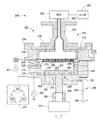
図2は、スペーサ層を形成するための堆積プロセスと、続いて選択的除去プロセスとを実行するための装置200の断面図である。本明細書に開示された教示と共に使用するのに適した処理チャンバは、例えば、カリフォルニア州サンタクララのアプライドマテリアルズ社から入手可能なHDP−Producer(登録商標)またはC3(登録商標)処理チャンバを含む。優れた堆積および選択的除去性能を可能にする複数の特徴を含む装置200が示されているが、他の処理チャンバが、本明細書に開示された発明の特徴のうちの1つ以上から利益を享受するように構成されてもよい。
FIG. 2 is a cross-sectional view of the
装置200は、処理チャンバ202と、処理チャンバ202に結合された遠隔プラズマ源204とを含む。遠隔プラズマ源204は、ラジカルを生成することができる任意の適切な源であってもよい。遠隔プラズマ源204は、高周波(RF)または非常に高い高周波(VHRF)容量結合プラズマ(CCP)源、誘導結合プラズマ(ICP)源、マイクロ波誘導(MW)プラズマ源、電子サイクロトロン共鳴(ECR)チャンバ、または高密度プラズマ(HDP)チャンバなどの遠隔プラズマ源であってもよい。遠隔プラズマ源204は、1つ以上のガス源206を含み、遠隔プラズマ源204は、ラジカル導管208によって処理チャンバ202に結合されてもよい。ラジカル生成ガスであり得る1つ以上のプロセスガスが、1つ以上のガス源206を介して遠隔プラズマ源204に入ることができる。1つ以上のプロセスガスは、塩素含有ガス、フッ素含有ガス、不活性ガス、酸素含有ガス、窒素含有ガス、水素含有ガス、またはこれらの任意の組み合わせを含むことができる。遠隔プラズマ源204で生成されたラジカルは、処理チャンバ202に結合されたラジカル導管208を通って処理チャンバ202内に移動し、処理チャンバ202内に画定された内部処理領域251に達する。
The
ラジカル導管208は、リッドアセンブリ212の一部であり、リッドアセンブリ212は、ラジカルキャビティ210、上部プレート214、リッドリム216、およびシャワーヘッド218も含む。ラジカル導管208は、ラジカルに対して実質的に非反応性の材料を含むことができる。例えば、ラジカル導管208は、AlN、SiO2、Y2O3、MgO、陽極酸化Al2O3、サファイア、セラミックであって、Al2O3、サファイア、AlN、Y2O3、MgOのうちの1つ以上を含むセラミック、またはプラスチックを含むことができる。適切なSiO2材料の代表例は、石英である。ラジカル導管208は、ラジカル導管支持部材220内に配置され、ラジカル導管支持部材220によって支持されてもよい。ラジカル導管支持部材220は、リッドリム216上に載っている上部プレート214上に配置することができる。
The
ラジカルキャビティ210は、ラジカル導管208の下方に配置され、ラジカル導管208に結合され、遠隔プラズマ源204で生成されたラジカルは、ラジカル導管208を通ってラジカルキャビティ210に移動する。ラジカルキャビティ210は、上部プレート214、リッドリム216、およびシャワーヘッド218によって画定される。任意選択で、ラジカルキャビティ210は、ライナ222を含むことができる。ライナ222は、ラジカルキャビティ210に露出された上部プレート214およびリッドリム216の表面を覆うことができる。遠隔プラズマ源204からのラジカルは、シャワーヘッド218内に配置された複数のチューブ224を通過して、内部処理領域251に入る。シャワーヘッド218は、複数のチューブ224よりも直径が小さい複数の開口部226をさらに含む。複数の開口部226は、複数のチューブ224と流体連通していない内部容積(図示せず)に接続されている。流体混合物を処理チャンバ202の内部処理領域251に導入するために、1つ以上の流体源219をシャワーヘッド218に結合することができる。流体混合物は、前駆体、ポロゲン、および/またはキャリア流体を含むことができる。流体混合物は、気体と液体との混合物であってもよい。
The
処理チャンバ202は、リッドアセンブリ212、チャンバ本体230、および支持アセンブリ232を含むことができる。支持アセンブリ232は、チャンバ本体230内に少なくとも部分的に配置されてもよい。チャンバ本体230は、処理チャンバ202の内部へのアクセスを提供するスリットバルブ235を含むことができる。チャンバ本体230は、チャンバ本体230の内面を覆うライナ234を含むことができる。ライナ234は、1つ以上の開孔236、および真空システム240と流体連通している、その中に形成されたポンピングチャネル238を含むことができる。開孔236は、ポンピングチャネル238へのガスの流路を提供し、ポンピングチャネル238は、処理チャンバ202内のガスの出口を提供する。
The
真空システム240は、真空ポート242と、バルブ244と、真空ポンプ246とを含むことができる。真空ポンプ246は、真空ポート242を介してポンピングチャネル238と流体連通している。開孔236は、ポンピングチャネル238がチャンバ本体230内の内部処理領域251と流体連通することを可能にする。内部処理領域251は、シャワーヘッド218の下面248および支持アセンブリ232の上面250によって画定され、内部処理領域251は、ライナ234によって囲まれている。
The
支持アセンブリ232は、チャンバ本体230内で処理するための基板(図示せず)を支持する支持部材252を含むことができる。基板は、例えば300mmなどの任意の標準的なウエハサイズであってもよい。あるいは、基板は、300mmより大きく、例えば450mm以上であってもよい。支持部材252は、動作温度に依存して、窒化アルミニウム(AlN)またはアルミニウムを含むことができる。支持部材252は、基板を支持部材252にチャッキングするように構成することができる。例えば、支持部材252は、静電チャックまたは真空チャックであってもよい。
The support assembly 232 can include a
支持部材252は、チャンバ本体230の底面に形成された中心に位置する開口部258を通って延びるシャフト256を介してリフト機構254に結合されてもよい。リフト機構254は、シャフト256の周囲からの真空漏れを防止するベローズ260によってチャンバ本体230に対してフレキシブルにシールすることができる。リフト機構254は、支持部材252が処理位置と下方の移送位置との間でチャンバ本体230内で垂直に移動することを可能にする。移送位置は、スリットバルブ235の開口部のわずかに下にある。動作中、基板表面におけるラジカルフラックスを最大にするために、基板とシャワーヘッド218との間の間隔を最小にすることができる。例えば、間隔は、約100mmと約5,000mmの間であってもよい。リフト機構254は、シャフト256を回転させることができ、シャフト256は、支持部材252を回転させ、支持部材252上に配置された基板を動作中に回転させる。
The
1つ以上の加熱要素262および冷却チャネル264が、支持部材252に埋め込まれてもよい。加熱要素262および冷却チャネル264は、動作中に基板の温度を制御するために使用されてもよい。加熱要素262は、1つ以上の抵抗加熱要素などの任意の適切な加熱要素であってもよい。加熱要素262は、1つ以上の電源(図示せず)に接続されてもよい。加熱要素262は、マルチゾーンの加熱または冷却に関する独立した加熱および/または冷却制御を有するように個々に制御することができる。マルチゾーンの加熱と冷却を独立して制御できるため、任意のプロセス条件で基板温度プロファイルを向上させることができる。冷却剤が、冷却チャネル264を通って流れて、基板を冷却することができる。支持部材252は、冷却ガスを基板の裏側に流すために上面250まで延びるガス通路をさらに含むことができる。
One or
RFソース電力243が、RFソース電力マッチングボックス247を介してシャワーヘッド218に結合することができる。RFソース電力243は、低周波数、高周波数、または非常に高い周波数であってもよい。一実施形態では、RFソース電力243は、高密度の膜層を堆積させるための高密度プラズマを生成する高周波RF発生器である。一例では、RFソース電力243は、支持部材252の上方の内部処理領域251で生成される誘導結合プラズマ(ICP)を生成し制御することができる誘導結合RFエネルギー伝送デバイスとして機能することができる。誘導結合プラズマ(ICP)を生成するとき、RFソース電力マッチングボックス247からの動的インピーダンス整合を提供することができる。
The
RFソース電力243に加えて、RFバイアス電源245を支持部材252に結合することができる。支持部材252は、カソードとして構成され、RFバイアス電源245に結合された電極263を含む。RFバイアス電源245は、支持部材252に配置された電極263と、シャワーヘッド218またはチャンバ本体230の天井(上部プレート214)などの別の電極との間に結合される。RFバイアス電源245から生成されたRFバイアス電力は、チャンバ本体230の内部処理領域251に配置されたガスから形成されたプラズマ放電を励起して維持する。
In addition to the
1つの動作モードにおいて、基板101が、処理チャンバ202内の支持部材252上に配置される。プロセスガスおよび/または混合ガスが、ガス源206からシャワーヘッド218を通ってチャンバ本体230に導入される。真空ポンプ246は、堆積副生成物を除去している間、チャンバ本体230内の圧力を維持する。
In one mode of operation, the
コントローラ270が、処理チャンバ202の動作を制御するために処理チャンバ202に結合される。コントローラ270は、処理シーケンスを制御し、ガス源206からのガス流を調整するために利用される中央処理装置(CPU)272、メモリ274、およびサポート回路276を含む。CPU272は、産業用の環境で使用されることができる任意の形態の汎用コンピュータプロセッサであってもよい。ソフトウェアルーチンは、ランダムアクセスメモリ、読み出し専用メモリ、フロッピー、またはハードディスクドライブ、または他の形式のデジタル記憶装置などのメモリ274に格納することができる。サポート回路276が、通常、CPU272に結合され、キャッシュ、クロック回路、入力/出力システム、電源などを含むことができる。コントローラ270と処理チャンバ202の様々な構成要素との間の双方向通信は、多数の信号ケーブルを通って処理される。
The
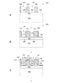
図3は、半導体デバイスのためのマルチパターニングプロセスの間にパターニング構造を形成するために後で使用され得るスペーサ層を基板上に堆積し、パターニングする方法300を示す。図4A〜図4Eは、方法300の様々な段階に対応する基板402の一部分の断面図である。一例では、スペーサ層を利用して、マルチパターニングプロセスの間に、またはマルチパターニングプロセス中に、基板表面上のパターニングされた構造に形成された開口部の寸法を縮小することができる。あるいは、方法300は、他のタイプの構造の残留物をエッチングまたは除去するために有益に利用されてもよい。
FIG. 3 shows a
方法300は、図4Aに示されるように、その上に形成された膜スタック400を有する基板、例えば図4Aに示される基板402を提供することによって工程302から開始する。基板402は、スペーサ層を堆積させてパターニングするために、図2に示す処理チャンバ202などの処理チャンバ内に移送することができる。基板402は、結晶シリコン(例えば、Si<100>又はSi<111>)、酸化ケイ素、歪シリコン、シリコンゲルマニウム、ゲルマニウム、ドープ又は非ドープポリシリコン、ドープ又は非ドープシリコンウェハ、パターン形成又は非パターン形成ウェハ、シリコン・オン・インシュレータ(SOI)、炭素ドープ酸化ケイ素、窒化ケイ素、ドープされたシリコン、ゲルマニウム、ヒ化ガリウム、ガラス、又はサファイアなどの材料であってよい。基板402は、200mm、300mm、450mmまたは他の直径などの様々な寸法を有することができ、さらに、長方形または正方形のパネルでもよい。特に明記しない限り、本明細書に記載される実施例は、直径200mm、直径300mm、または直径450mmの基板上で実施される。
膜スタック400は、基板402上に配置された少なくとも1つの誘電体層404を含み、これは、基板402へのフィーチャの転写を容易にするために別のパターニングされた構造を形成するために後で利用され得る。図4Aに示す実施形態では、誘電体層404が基板402上に形成される。誘電体層404は、必要に応じて直接的または間接的に(例えば、追加の層または構造が、誘電体層404と基板402との間に形成される)接触して形成されてもよいことに留意されたい。
一実施形態では、誘電体層404は、酸化ケイ素、窒化ケイ素、酸窒化ケイ素、高誘電率材料、またはそれらの組み合わせなどである。本明細書で言及される高誘電率材料は、4.0より大きい誘電率を有する誘電体材料である。高誘電率材料層の適切な例は、二酸化ハフニウム(HfO2)、二酸化ジルコニウム(ZrO2)、ハフニウムシリコン酸化物(HfSiO2)、ハフニウムアルミニウム酸化物(HfAlO)、ジルコニウムシリコン酸化物(ZrSiO2)、二酸化タンタル(TaO2)、酸化アルミニウム、アルミニウムをドープした二酸化ハフニウム、ビスマスストロンチウムチタン(BST)、および白金ジルコニウムチタン(PZT)などを含む。図4Aに示す実施形態では、誘電体層404は、約10nmと約300nmの間の厚さを有する酸化ケイ素層である。
In one embodiment, the
その中に形成された複数の開口部410(例えば、開口部の第1の群)を有するパターニングされた構造408を誘電体層404上に配置し、誘電体層404の一部406を露出させて、望む通りに、基板402上に配置された膜スタック400内に所望の半導体構造を形成するように、誘電体層404へのフィーチャの転写を容易にすることができる。パターニングされた構造408は、必要に応じて単一層または複合層であってよい。一実施形態では、パターニングされた構造408は、ポリシリコン、結晶シリコン、アモルファスシリコン、ドープされたシリコン材料、アモルファスカーボン材料、窒化ケイ素、二酸化ケイ素、炭化ケイ素、または任意の適切なケイ素含有材料などのケイ素含有材料から製造することができる。1つの特定の例では、パターニングされた構造408は、アモルファスシリコン層またはポリシリコン層から製造される。
A
工程304において、スペーサ層416が、図4Bに示すように、パターニングされた構造408の側壁415および上面418ならびに誘電体層404の一部406の上に共形的に形成される。スペーサ層416は、図2に示す処理チャンバ202などのプラズマ処理チャンバ内で形成される。スペーサ層416は、誘電体層404のために選択された材料と異なる誘電体材料であってもよい。一例では、スペーサ層416は、ポリシリコン層、微結晶シリコン層、ナノ結晶層、アモルファスシリコン層などのケイ素含有層である。スペーサ層416は、HDP−CVDプロセス、エピタキシャル堆積プロセス、ファーネスプロセス、ALDプロセス、またはPVD、CVD、ALD、もしくは他の適切なプラズマ処理チャンバ内の任意の適切な堆積技術によって形成することができる。1つの特定の例では、スペーサ層416は、約7nm〜約25nmの厚さを有する、処理チャンバ202内で行われる高密度プラズマ(HDP)CVDプロセスによって形成されたアモルファスシリコン層(a−Si)である。スペーサ層416の適切な例示的な材料には、アモルファスシリコン、ポリシリコン、アモルファスカーボン材料、窒化ケイ素、二酸化ケイ素または炭化ケイ素が含まれる。
In
一例では、スペーサ層416の堆積中に、堆積混合ガスを処理チャンバ202に供給して処理することができる。一実施形態では、混合ガスは、少なくともシラン系ガスを含むことができる。シラン系ガスの適切な例としては、シラン(SiH4)、ジシラン(Si2H6)、四フッ化ケイ素(SiF4)、四塩化ケイ素(SiCl4)、ジクロロシラン(SiH2Cl2)等が挙げられる。
In one example, during the deposition of the
いくつかの例では、キャリアガスを堆積中に混合ガスに供給することもできる。キャリアガスの適切な例は、N2,N2O,NO2,NH3,CO,CO2,O2,O3,H2Oなどを含む。任意選択で、He、Ar、Kr、Neなどの不活性ガスを混合ガスに供給することもできる。ある特定の例では、混合ガスで使用されるシラン系ガスは、シラン(SiH4)またはジシラン(Si2H6)であり、キャリアガスはN2であり、不活性ガスはHeであり、アモルファスシリコン(a−Si)層または窒化ケイ素層が形成される。 In some examples, carrier gas can also be supplied to the mixed gas during deposition. Suitable examples of carrier gases include N 2, N 2 O, NO 2, NH 3, CO, CO 2, O 2, O 3, H 2 O and the like. An inert gas such as He, Ar, Kr, or Ne can be optionally supplied to the mixed gas. In one particular example, the silane-based gas used in the mixed gas is silane (SiH 4 ) or disilane (Si 2 H 6 ), the carrier gas is N 2 , the inert gas is He, and amorphous. A silicon (a-Si) layer or a silicon nitride layer is formed.
一例では、N2ガスに対するシラン系ガスのガス比を維持して、混合ガスの反応挙動を制御して、所望の膜特性を生成する。一実施形態では、シラン系ガスとN2ガスとのガス比は、約1:3〜約1:5に制御することができる。 In one example, the gas ratio of the silane gas to the N 2 gas is maintained to control the reaction behavior of the mixed gas to produce the desired membrane properties. In one embodiment, the gas ratio of silane gas and N 2 gas is about 1: 3 to about 1: it is possible to control the 5.
堆積中、誘導結合プラズマ(ICP)電力などのRFソース電力が、スペーサ層416を堆積させるために利用されてもよい。スペーサ層416を堆積するために利用されるRFソース電力、すなわちICP電力は、所望のエッチング速度を有する所望の密度または応力などの所望の膜特性を有するスペーサ層416の形成を助けることができる。一例では、650ワット未満、例えば約200ワット〜約600ワット、例えば約500ワットなどの比較的低いRFソース電力を、堆積中に処理チャンバ202に供給することができる。約600W未満、例えば100ワット〜約500ワットなどの比較的低いRFバイアス電力を、堆積中に処理チャンバ202に供給することもできる。堆積プロセス中に、比較的低いRFバイアス電力とともに、650ワット未満などの、誘導結合プラズマ(ICP)電力を伴う比較的低いRFソース電力を利用することにより、プラズマ密度が低くなり、混合ガスからのイオンの解離を高める可能性のあるイオン衝突を減じると考えられる。しかしながら、各格子単位の中に閉じ込められた過剰なケイ素元素は、膜密度を増加させるだけでなく、後続のパターニングプロセス中に良好な膜エッチング/侵食抵抗を提供することができる高い応力をもたらす。
During deposition, RF source power, such as inductively coupled plasma (ICP) power, may be utilized to deposit the
堆積中、基板温度は、セ氏約200度〜セ氏約450度、例えばセ氏約350度に制御することができる。シラン(SiH4)などのシラン系ガスが、約8sccm〜約60sccm、例えば約30sccm〜約40sccmなどの流量で混合ガスに供給されてもよい。Heガスなどの不活性ガスが、約200sccm〜約2000sccm、例えば約600sccm〜約1200sccmなどの流量で混合ガスに供給されてもよい。N2ガスなどのキャリアガスが、約60sccm〜約200sccm、例えば約120sccm〜約160sccmの流量で混合ガスに供給されてもよい。混合ガスから形成されたプラズマを維持するために、約400ワット〜約2000ワット、例えば450ワット〜約1000ワットのRFソース電力が印加されてもよい。プロセス圧力が、約5mTorr〜約100mTorr、例えば約15mTorr〜約50mTorrに維持されてもよい。基板とシャワーヘッドとの間の間隔が、約200ミル〜約6000ミルに制御されてもよい。堆積プロセスが、約2秒〜約100秒の間、例えば約5秒〜約10秒の間、実施されてもよい。 During deposition, the substrate temperature can be controlled from about 200 degrees Celsius to about 450 degrees Celsius, for example about 350 degrees Celsius. A silane-based gas such as silane (SiH 4 ) may be supplied to the mixed gas at a flow rate of about 8 sccm to about 60 sccm, for example, about 30 sccm to about 40 sccm. An inert gas such as He gas may be supplied to the mixed gas at a flow rate of about 200 sccm to about 2000 sccm, for example about 600 sccm to about 1200 sccm. A carrier gas such as N 2 gas may be supplied to the mixed gas at a flow rate of about 60 sccm to about 200 sccm, for example about 120 sccm to about 160 sccm. RF source power of about 400 watts to about 2000 watts, for example 450 watts to about 1000 watts, may be applied to maintain the plasma formed from the mixed gas. The process pressure may be maintained from about 5 mTorr to about 100 mTorr, for example from about 15 mTorr to about 50 mTorr. The distance between the substrate and the shower head may be controlled from about 200 mils to about 6000 mils. The deposition process may be carried out for about 2 seconds to about 100 seconds, for example about 5 seconds to about 10 seconds.
さらに、スペーサ層416を基板402上に堆積する前に、基板前処理プロセスを、工程304で実行される堆積プロセスに先立って実行してもよい。前処理プロセスは、処理チャンバ202などの、工程304における堆積プロセスが実行される同じ処理チャンバ内でインシトゥで実行されてもよい。前処理プロセスおよび工程304における堆積プロセスは、処理のためにコントローラ270に格納された単一のレシピですべて調整および整理されてもよい。あるいは、前処理プロセスおよび工程304における堆積プロセスは、異なるレシピに格納され、必要に応じて中断することなく連続して実行されてもよい。
Further, the substrate pretreatment process may be performed prior to the deposition process performed in
前処理プロセスの間、基板402は、基板402がその上に位置する支持部材252を加熱することによって、所望の温度範囲に予熱されてもよい。一実施形態では、基板温度は、摂氏約25度、すなわち室温から、摂氏約200度と摂氏約450度の間、例えば摂氏約350度に制御することができる。前処理プロセス中に、ICPソース電力などのRFソース電力が、印加されてもよい。RFソース電力は、約1500ワット〜約2500ワット、例えば約2000ワットの上部ソース電力と、約3000ワット〜約5000ワット、例えば約4000ワットの側部ソース電力を有するように、処理チャンバに供給されてもよい。前処理プロセスの間、約5mTorr〜約15mTorrのプロセス圧力が、維持されてもよい。前処理混合ガスが、Ar、He、Ne、またはKrなどの少なくとも不活性ガスを含み、前処理プロセスの間に供給されてもよい。一例では、前処理混合ガスは、前処理プロセスの間、約5:1〜約1:5、例えば約1:1〜約1:2の比率で処理チャンバに供給されるArガスおよびHeガスを含むことができる。前処理プロセスは、約30秒〜約90秒、例えば約50秒の間、行われてもよい。
During the pretreatment process, the
工程306において、堆積後処理プロセスが、スペーサ層の特定の部分を選択的に処理するために実行される。堆積後処理プロセス中に生成されたプラズマからのイオンの制御された軌道及び指向性により、所望の結果の膜形状をもたらすようにスペーサ層416を効率的に切るような、制御された処理の寄与が得られると考えられる。一実施形態では、図4Cに示すように、工程306中に実行される堆積後処理プロセスは、スペーサ層416の特に上面424および底面425上に処理された層を優勢に形成することができる。その結果、プラズマからの活性処理種は、他の部分、例えばスペーサ層416のコーナー部422および側壁415を著しく攻撃、侵食または損傷することなく、スペーサ層416の特定の部分、例えば、上面424または底面425のみを選択的に処理することができ、処理プロセス後にスペーサ層416の良好な形状を得る。そうすることによって、丸みのあるコーナー部、ファセットコーナー、侵食された側壁、または変形した形状がスペーサ層416に形成される可能性を、効率的に低減または排除することができる。
In
工程306の堆積後処理プロセスで生成されたプラズマから提供されるイオン/ラジカルは、特に上面424または底面425におけるスペーサ層416の膜特性の一部を変化させ、および/または変更し、その結果、処理された領域、例えば上面424または底面425の膜結合構造は、スペーサ層416の側壁415およびコーナー部422などの他の領域と異なるようになる。処理された領域(例えば、上面424または底面425)と処理されていない領域(例えば、側壁415およびコーナー部422)との間の膜特性の相違は、処理された領域とスペーサ層416から残る他の材料との間の自然なエッチング障壁を提供し、したがって、後続の選択的除去プロセスにおける動作中に高い選択性を提供する。
The ions / radicals provided by the plasma generated during the post-deposition treatment process of
堆積後処理プロセスは、必要に応じて所望の形状/膜結合構造の変化を形成するように、上面424または底面425などの処理された領域を形成するように結合構造を変更し、その後の選択的除去プロセスの間に異なるプロセス結果を得ることができる変更された膜特性を有する、上面424または底面425などの処理された領域を提供する。
The post-deposition treatment process modifies the bond structure to form a treated area such as top 424 or bottom 425 to form the desired shape / membrane bond structure change as needed, followed by selection. Provided are treated areas such as
工程306における堆積後処理プロセスの間にプラズマに印加される電力は、不活性ガスなどの堆積後処理混合ガスからの原子に運動量を提供することができるので、上面424または底面425からの原子と衝突すると、上面424または底面425の結合構造が損傷して再配置され、その結果、スペーサ層416の側壁415およびコーナー部422などの処理されていない領域と比較して、処理されるように選択された領域に損傷した/緩い結合構造が生じる可能性がある。不活性ガスからの原子が、上面424または底面425に存在する結合構造を損傷し、緩めるので、処理後の上面424または底面425は、除去プロセスによって容易に除去することができる損傷した結合構造を有することがある。
The power applied to the plasma during the post-deposition treatment process in
一例では、堆積後処理混合ガスは、工程306における堆積後処理プロセス中に、供給されてもよい。堆積後処理混合ガスは、堆積後処理プロセスを実行するために、制御された指向性(例えば、指向性バイアス電力によって制御される)を有するAr、Ne、He、またはKrなどの少なくとも不活性ガス、および/またはH2ガスを含むことができる。不活性ガスからの原子は、効率的な衝突を提供して、スペーサ層416の上面424または底面425の格子/結合構造を変更し、損傷させて、工程306で行われる次の選択的除去プロセスを容易にするような、スペーサ層416の上面424または底面425に衝突する所望の衝突力を提供することができる。
In one example, the post-deposition treatment mixed gas may be supplied during the post-deposition treatment process in
いくつかのプロセスパラメータが、工程306での堆積後処理プロセス中に制御されてもよい。Heガスなどの不活性ガスは、約200sccmと約1200sccmとの間の流量で処理チャンバに供給することができる。チャンバ圧力は、一般に、約10mTorrと約100mTorrとの間、例えば約20mTorrに維持される。基板温度は、セ氏約100度とセ氏約450度との間、例えばセ氏約350度に制御することができる。処理中に堆積後処理混合ガスを解離させるのを助けるために、容量性または誘導性RF電力などのRFバイアス電力、DC電力、電磁エネルギー、またはマグネトロンスパッタリングを、処理チャンバ202に供給することができる。解離エネルギーによって生成されたイオンは、支持部材252にRFバイアス電力を印加することによって生成された電界を用いて、基板に向かって加速されてもよい。一実施形態では、約13.56MHzの周波数を有するRFバイアス電力が、約50ワット〜約1500ワット、例えば約100ワットの電力レベルで支持部材252をバイアスするように供給される。このようにして生成されたイオンは、一般に、上述のように基板またはガス分配器をバイアスすることによって、上面424および底面425などの所望の領域に基板に向かって加速される。一実施形態では、工程306での堆積後処理プロセス中に、RFソース電力が、処理チャンバ202に任意選択で印加されてもよい。1つの特定の例では、RFバイアス電力は、RFソース電力が印加されない状態で、約100ワットに制御される。
Some process parameters may be controlled during the post-deposition treatment process in
次に、工程308において、残留物除去プロセスが実行されて、図4Dに示されるように、基板402から上面424および底面425などの処理された領域が除去され、所望の形状および寸法を有するスペーサ層416が形成される。除去混合ガスが、図2に示す処理チャンバ202における遠隔プラズマ源204などの遠隔プラズマ源を有する処理チャンバ内に供給され、パターニングされた構造408の上面418および誘電体層404の一部406が露出されるまで、上面424および底面425などの処理された領域を除去する。上述したように、上面424および底面425などの処理された領域は、除去プロセス中にエッチングバリア層として機能するスペーサ層416の側壁415およびコーナー部422と比較して、異なる膜特性を有し、スペーサ層416の側壁415およびコーナー部422を損傷または攻撃することなく、上面424および底面425などの処理された領域を選択的に除去するだけである高い選択性をもたらす。
Next, in
上面424および底面425などの処理された領域を除去するために選択された除去混合ガスは、基板402から上面424および底面425を除去するために遠隔プラズマ源から供給された混合ガスを含む。遠隔プラズマ除去プロセスは、基板402上の上面424および底面425を、他の表面を実質的に攻撃することなく、ゆっくりと選択的に除去するために行われる穏やかな除去プロセスである。遠隔プラズマ除去プロセスは、除去混合ガスを処理チャンバ202に供給して、除去混合ガスから遠隔プラズマを形成することによって実行される。
The removal mixed gas selected to remove the treated areas such as the
一実施形態では、上面424および底面425などの処理された領域を除去するために使用される除去混合ガスは、アンモニア(NH3)ガスおよび三フッ化窒素(NF3)ガスの混合ガスである。除去混合ガスに使用されるアンモニア(NH3)ガスは、必要に応じてN2ガスに置き換えることができる。さらに、除去効率を改善するために、H2、Ar、Heなどのガスが、除去混合ガスに加えられてもよい。処理チャンバに導入される各ガスの量は、例えば、除去されるスペーサ層416の厚さ、処理される基板の形状寸法、プラズマキャビティの容積容量、チャンバ本体の容積容量、ならびにチャンバ本体に結合された真空システムの能力に適応するように変更され調整されてもよい。
In one embodiment, the removal mixed gas used to remove the treated areas such as the top 424 and bottom 425 is a mixed gas of ammonia (NH 3 ) gas and nitrogen trifluoride (NF 3 ) gas. .. The ammonia (NH 3 ) gas used in the removal mixed gas can be replaced with N 2 gas if necessary. Furthermore, in order to improve the removal efficiency, H 2, Ar, gas such as He, may be added to remove the gas mixture. The amount of each gas introduced into the processing chamber is coupled to, for example, the thickness of the
プラズマが、遠隔プラズマ源204で遠隔に生成されると、遠隔プラズマからの除去混合ガスから解離したエッチング剤は、比較的穏和で穏やかであるため、図4Dに示すように、パターニングされた構造408および誘電体層404が露出するまで、上面424および底面425などの処理された領域を、ゆっくり穏やかにかつ徐々に化学的に反応させる。遠隔プラズマ源では、アンモニア(NH3)ガスおよび三フッ化窒素(NF3)ガスが、遠隔プラズマ源204において解離され、フッ化アンモニウム(NH4F)および/またはHFを伴うフッ化アンモニウム(NH4F.HF)を形成すると考えられる。フッ化アンモニウム(NH4F)及びHFを伴うフッ化アンモニウム(NH4F.HF)のエッチング剤が、処理チャンバ202の内部処理領域251に導入されると、フッ化アンモニウム(NH4F)及びHFを伴うフッ化アンモニウム(NH4F.HF)のエッチング剤は、基板に到達すると、上面424および底面425などの処理された領域と反応し、基板402から除去されるべきNH4含有塩を形成し得る。フッ化アンモニウム(NH4F)及びHFを伴うフッ化アンモニウム(NH4F.HF)のエッチング剤は、上面424および底面425などの処理された領域を化学的に反応させ、気体状態または固体状態でNH4含有塩を形成し、これは気体状態では処理チャンバから排気され、固体状態においては、後で低温昇華プロセスを用いて基板表面から除去される。
When the plasma is generated remotely at the
1つ以上の実施形態において、アンモニア(NH3)対三フッ化窒素(NF3)のモル比が少なくとも1:1である除去混合ガスを提供するように、ガスが加えられる。1つ以上の実施形態において、除去混合ガスのモル比は、少なくとも約3:1(アンモニア対三フッ化窒素)である。これらのガスは、約5:1(アンモニア対三フッ化窒素)から約20:1のモル比で処理チャンバ202に導入される。さらに別の実施形態において、エッチング混合ガスのモル比は、約5:1(アンモニア対三フッ化窒素)から約10:1である。
In one or more embodiments, the gas is added to provide a removal mixed gas with a molar ratio of ammonia (NH 3 ) to nitrogen trifluoride (NF 3 ) of at least 1: 1. In one or more embodiments, the molar ratio of the removed mixed gas is at least about 3: 1 (ammonia to nitrogen trifluoride). These gases are introduced into the
一実施形態では、除去混合ガスを処理チャンバ202の内部処理領域251に運ぶのを助けるために、不活性ガスまたはキャリアガスなどの他のタイプのガスが、除去混合ガスに供給されてもよい。不活性ガスまたはキャリアガスの適切な例は、Ar,He,N2,H2,O2,N2O,NO2,NOなどのうちの少なくとも1つを含む。一実施形態では、不活性ガスまたはキャリアガスは、ArまたはHeおよびH2またはN2であり、約500sccm〜約2000sccmの体積流量で処理チャンバ202に供給されてもよい。
In one embodiment, another type of gas, such as an inert gas or carrier gas, may be supplied to the removed mixed gas to aid in transporting the removed mixed gas to the
遠隔プラズマ源エッチング/除去プロセスを実行するために除去混合ガスを供給する間、基板温度は、セ氏約40度〜セ氏約150度の範囲、例えばセ氏約100度に維持されてもよい。前処理プロセス、工程304の堆積プロセス、および工程306の堆積後処理プロセスにおいて、高い温度、例えばセ氏約350度と比較して、セ氏約100度の比較的低い温度が、処理されていない領域を攻撃または損傷させることなく、処理された領域が穏和に/穏やかに除去され、選択的除去プロセスを成功させることができるように、処理領域除去プロセスを安定化させ、安定して実行されるのに役立ち得ることに留意されたい。
The substrate temperature may be maintained in the range of about 40 degrees Celsius to about 150 degrees Celsius, eg, about 100 degrees Celsius, while supplying the removal mixed gas to perform the remote plasma source etching / removal process. In the pretreatment process, the deposition process of
除去混合ガスが処理チャンバに供給された後、上面424および底面425などの処理された領域が、エッチングされ除去されて、アンモニウム塩などの固体エッチング副生成物を、もしあれば基板表面に残すことができる。基板402上に残っているアンモニウム塩などのエッチング副生成物は、セ氏約100度などの比較的低い融点を有し、工程308の選択的除去プロセス後に行われる昇華プロセスによって副生成物を基板から除去することを可能にする 。昇華プロセスは、工程304で堆積プロセスを実行する前の、上述した前処理プロセスと同じであってもよい。図3に示すループ310によって示されるように、工程304における堆積プロセス、工程306における堆積後プロセスおよび工程308における選択的除去プロセスを、必要な回数だけ繰り返し実行することができるので、工程308でのエッチング副生成物を除去するために利用される昇華プロセスは、上述のように工程304での堆積プロセスの前に行われる前処理プロセスであってもよい。一実施形態では、工程304から工程308が実行されるサイクル数は、約2回から約10回であってもよい。
After the removal gas is fed to the processing chamber, the treated areas such as the top 424 and bottom 425 are etched and removed, leaving solid etching by-products such as ammonium salts on the substrate surface, if any. Can be done. Etching by-products such as ammonium salts remaining on the
工程308におけるエッチング/除去プロセスの間に、いくつかのプロセスパラメータを調整して、エッチング/除去プロセスを制御することができる。1つの例示的な実施形態では、処理チャンバ202内のプロセス圧力は、約500mTorr〜約5000mTorr、例えば約1500mTorrに調整される。遠隔プラズマを供給するために、約70KHzの周波数のRPSを印加することができる。例えば、約20ワット〜約60ワット、例えば約40ワットのRPS電力をエッチング混合ガスに印加することができる。
During the etching / removal process in
所望の形状を有するスペーサ層416が基板402上に形成された後、図4Eに示されるように、基板402からパターニングされた構造408を除去するためにポストエッチングプロセスが実行され、後続の製造プロセスのためのエッチングマスクとして、間に画定された縮小された寸法の開口部440(例えば、開口部の第2の群)を有するスペーサ層416を残す。ポストエッチング混合ガスが、実質的にスペーサ層416をエッチングまたは損傷することなく、パターニングされた構造408を選択的かつ優勢にエッチングするために、実行されてもよい。
After the
前処理プロセス、工程304における堆積プロセス、工程306における堆積後処理プロセス、工程308における選択的除去プロセス、および選択的除去プロセス後にパターニングされた構造408を除去するために実施される任意選択のポストエッチングプロセスが、全て同じ処理チャンバ内で(例えば、インシトゥで)実行されてもよい。
Pretreatment process, deposition process in
このように、所望のエッジ/コーナー形状を有するパターニングされたスペーサ層を生成するために、マルチパターニングプロセスを実行するためのスペーサ層をパターニングする実施形態が提供される。スペーサ層堆積及びパターニングプロセスの間に前処理プロセス、堆積プロセス、後堆積処理プロセス及び選択的エッチングプロセスを利用することにより、制御されたイオン軌道/指向性が得られ、所望の正確で直角のコーナー部及び垂直な側壁形状を有するパターニングされたスペーサ層を生じる所望の方法でスペーサ層をパターニングすることができる。 As described above, an embodiment of patterning the spacer layer for performing a multi-patterning process is provided in order to generate a patterned spacer layer having a desired edge / corner shape. By utilizing pretreatment, deposition, post-deposition and selective etching processes between spacer layer deposition and patterning processes, controlled ion trajectories / orientations are obtained with the desired accurate and perpendicular corners. The spacer layer can be patterned in any way that results in a patterned spacer layer with portions and vertical side wall shapes.
上記は本発明の実施形態を対象とするが、本発明の基本的な範囲から逸脱することなく、本発明の他のさらなる実施形態を考え出すこともでき、本発明の範囲は、以下の特許請求の範囲によって決定される。 Although the above is intended for embodiments of the present invention, other further embodiments of the present invention may be conceived without departing from the basic scope of the invention, and the scope of the present invention is the following claims. Determined by the range of.
Claims (15)
基板上に配置されたパターニングされた構造であって、その間に画定された開口部の第1の群を有するパターニングされた構造の外面上にスペーサ層を共形的に形成することと、
前記基板上に形成された前記スペーサ層の第1の部分を、前記スペーサ層の第2の部分を処理することなく、選択的に処理することと、
前記スペーサ層の処理された前記第1の部分を選択的に除去することと
を含む方法。 A method of depositing and patterning spacer layers during a multi-patterning process.
Conformally forming a spacer layer on the outer surface of a patterned structure arranged on a substrate with a first group of openings defined between them.
To selectively treat the first portion of the spacer layer formed on the substrate without treating the second portion of the spacer layer.
A method comprising selectively removing the treated first portion of the spacer layer.
不活性ガスを含む前処理混合ガスを前記基板に供給することと、
前記基板の温度をセ氏約200度からセ氏約400度の間に維持することと
をさらに含む、請求項4に記載の方法。 Pretreatment of the substrate can be
Supplying the pretreated mixed gas containing an inert gas to the substrate and
The method of claim 4 , further comprising maintaining the temperature of the substrate between about 200 degrees Celsius and about 400 degrees Celsius.
前記堆積混合ガスに6500ワット未満の誘導結合ソース電力を印加することと、
前記堆積混合ガスに100ワットから約500ワットの間のRFバイアス電力を印加することと
をさらに含む、請求項7に記載の方法。 Supplying the deposited mixed gas can
Applying less than 6500 watts of inductively coupled source power to the sedimentary mixed gas,
The method of claim 7, further comprising applying RF bias power between 100 watts and about 500 watts to the deposited mixed gas.
アンモニア(NH3)ガスと三フッ化窒素(NF3)ガスとを含む選択的除去混合ガスを供給することと、
遠隔プラズマ源を前記選択的除去混合ガスに印加することと
をさらに含む、請求項1から11のいずれか一項に記載の方法。 To selectively remove the treated first portion of the spacer layer
Supplying a selective removal mixed gas containing ammonia (NH 3 ) gas and nitrogen trifluoride (NF 3 ) gas, and
Further comprising a to mark pressurizing the remote plasma source to the selective removal mixed gas, the method according to any one of claims 1 to 11.
前記開口部の第1の群の寸法よりも小さい寸法を有する開口部の第2の群を、エッチングされた前記スペーサ層に形成することと
をさらに含む、請求項1から13のいずれか一項に記載の方法。 Removing the patterned structure from the substrate and
Any one of claims 1 to 13 , further comprising forming a second group of openings in the etched spacer layer having a size smaller than the size of the first group of openings. The method described in.
Applications Claiming Priority (3)
| Application Number | Priority Date | Filing Date | Title |
|---|---|---|---|
| US14/729,932 | 2015-06-03 | ||
| US14/729,932 US9484202B1 (en) | 2015-06-03 | 2015-06-03 | Apparatus and methods for spacer deposition and selective removal in an advanced patterning process |
| PCT/US2016/033882 WO2016196073A1 (en) | 2015-06-03 | 2016-05-24 | Apparatus and methods for spacer deposition and selective removal in an advanced patterning process |
Publications (2)
| Publication Number | Publication Date |
|---|---|
| JP2018516463A JP2018516463A (en) | 2018-06-21 |
| JP6810059B2 true JP6810059B2 (en) | 2021-01-06 |
Family
ID=57189280
Family Applications (1)
| Application Number | Title | Priority Date | Filing Date |
|---|---|---|---|
| JP2017562685A Active JP6810059B2 (en) | 2015-06-03 | 2016-05-24 | Equipment and methods for spacer deposition and selective removal in advanced patterning processes |
Country Status (6)
| Country | Link |
|---|---|
| US (1) | US9484202B1 (en) |
| JP (1) | JP6810059B2 (en) |
| KR (1) | KR102483741B1 (en) |
| CN (1) | CN107735851B (en) |
| TW (1) | TWI627724B (en) |
| WO (1) | WO2016196073A1 (en) |
Families Citing this family (17)
| Publication number | Priority date | Publication date | Assignee | Title |
|---|---|---|---|---|
| US20170345673A1 (en) * | 2016-05-29 | 2017-11-30 | Tokyo Electron Limited | Method of selective silicon oxide etching |
| KR102347402B1 (en) * | 2016-05-29 | 2022-01-04 | 도쿄엘렉트론가부시키가이샤 | Sidewall image transfer method |
| US10858727B2 (en) | 2016-08-19 | 2020-12-08 | Applied Materials, Inc. | High density, low stress amorphous carbon film, and process and equipment for its deposition |
| US10276379B2 (en) * | 2017-04-07 | 2019-04-30 | Applied Materials, Inc. | Treatment approach to improve film roughness by improving nucleation/adhesion of silicon oxide |
| KR102509390B1 (en) * | 2017-07-24 | 2023-03-14 | 어플라이드 머티어리얼스, 인코포레이티드 | Pretreatment Approach to Improve Continuity of Ultrathin Amorphous Silicon Films on Silicon Oxide |
| US10147611B1 (en) | 2017-08-28 | 2018-12-04 | Nanya Technology Corporation | Method for preparing semiconductor structures |
| US10607852B2 (en) * | 2017-09-13 | 2020-03-31 | Tokyo Electron Limited | Selective nitride etching method for self-aligned multiple patterning |
| KR20190035036A (en) * | 2017-09-25 | 2019-04-03 | 삼성전자주식회사 | Apparatus for forming a layer on a substrate and method of forming an amorphous silicon layer on a substrate using the same |
| US10636675B2 (en) | 2017-09-27 | 2020-04-28 | Applied Materials, Inc. | Methods of etching metal-containing layers |
| US10734228B2 (en) * | 2017-12-19 | 2020-08-04 | Tokyo Electron Limited | Manufacturing methods to apply stress engineering to self-aligned multi-patterning (SAMP) processes |
| US11114306B2 (en) * | 2018-09-17 | 2021-09-07 | Applied Materials, Inc. | Methods for depositing dielectric material |
| US11551930B2 (en) * | 2018-12-12 | 2023-01-10 | Tokyo Electron Limited | Methods to reshape spacer profiles in self-aligned multiple patterning |
| CN111384172B (en) * | 2018-12-29 | 2024-01-26 | 中芯国际集成电路制造(上海)有限公司 | Semiconductor device and method of forming the same |
| US10629451B1 (en) * | 2019-02-01 | 2020-04-21 | American Air Liquide, Inc. | Method to improve profile control during selective etching of silicon nitride spacers |
| CN109979816A (en) * | 2019-03-26 | 2019-07-05 | 上海华力集成电路制造有限公司 | Improve the method for isolation side walls pattern |
| US11355342B2 (en) * | 2019-06-13 | 2022-06-07 | Nanya Technology Corporation | Semiconductor device with reduced critical dimensions and method of manufacturing the same |
| CN113496895A (en) * | 2020-04-01 | 2021-10-12 | 中芯国际集成电路制造(上海)有限公司 | Method for forming semiconductor structure |
Family Cites Families (24)
| Publication number | Priority date | Publication date | Assignee | Title |
|---|---|---|---|---|
| US6949203B2 (en) * | 1999-12-28 | 2005-09-27 | Applied Materials, Inc. | System level in-situ integrated dielectric etch process particularly useful for copper dual damascene |
| CN100451831C (en) * | 2001-10-29 | 2009-01-14 | 旺宏电子股份有限公司 | Method of reducing size of pattern interval of opening |
| US7271107B2 (en) * | 2005-02-03 | 2007-09-18 | Lam Research Corporation | Reduction of feature critical dimensions using multiple masks |
| US7807575B2 (en) * | 2006-11-29 | 2010-10-05 | Micron Technology, Inc. | Methods to reduce the critical dimension of semiconductor devices |
| CN101339361A (en) * | 2007-06-01 | 2009-01-07 | 应用材料公司 | Frequency doubling using spacer mask |
| JP5254351B2 (en) * | 2007-11-08 | 2013-08-07 | ラム リサーチ コーポレーション | Pitch reduction using oxide spacers |
| US20090286402A1 (en) * | 2008-05-13 | 2009-11-19 | Applied Materials, Inc | Method for critical dimension shrink using conformal pecvd films |
| US8232212B2 (en) * | 2008-07-11 | 2012-07-31 | Applied Materials, Inc. | Within-sequence metrology based process tuning for adaptive self-aligned double patterning |
| US8361338B2 (en) * | 2010-02-11 | 2013-01-29 | Taiwan Semiconductor Manufacturing Company, Ltd. | Hard mask removal method |
| US9390909B2 (en) * | 2013-11-07 | 2016-07-12 | Novellus Systems, Inc. | Soft landing nanolaminates for advanced patterning |
| US8728956B2 (en) * | 2010-04-15 | 2014-05-20 | Novellus Systems, Inc. | Plasma activated conformal film deposition |
| KR20120121795A (en) * | 2011-04-27 | 2012-11-06 | 에스케이하이닉스 주식회사 | Method for manufacturing of semiconductor device having spacer with air gap |
| US8609548B2 (en) * | 2011-06-06 | 2013-12-17 | Lam Research Corporation | Method for providing high etch rate |
| KR101835114B1 (en) | 2011-09-07 | 2018-03-06 | 삼성전자주식회사 | Three Dimensional Semiconductor Device And Method Of Fabricating The Same |
| US8431461B1 (en) * | 2011-12-16 | 2013-04-30 | Lam Research Corporation | Silicon nitride dry trim without top pulldown |
| US20130189845A1 (en) * | 2012-01-19 | 2013-07-25 | Applied Materials, Inc. | Conformal amorphous carbon for spacer and spacer protection applications |
| US8980111B2 (en) | 2012-05-15 | 2015-03-17 | Tokyo Electron Limited | Sidewall image transfer method for low aspect ratio patterns |
| CN102709230B (en) * | 2012-05-22 | 2015-05-20 | 上海华力微电子有限公司 | Method for forming semiconductor through hole |
| CN103779211B (en) * | 2012-10-18 | 2017-02-01 | 中芯国际集成电路制造(上海)有限公司 | Manufacturing method for semiconductor device |
| US9362133B2 (en) * | 2012-12-14 | 2016-06-07 | Lam Research Corporation | Method for forming a mask by etching conformal film on patterned ashable hardmask |
| US20150014772A1 (en) | 2013-07-11 | 2015-01-15 | International Business Machines Corporation | Patterning fins and planar areas in silicon |
| US9318412B2 (en) | 2013-07-26 | 2016-04-19 | Nanya Technology Corporation | Method for semiconductor self-aligned patterning |
| US9159579B2 (en) | 2013-10-25 | 2015-10-13 | Taiwan Semiconductor Manufacturing Company, Ltd. | Lithography using multilayer spacer for reduced spacer footing |
| TWI531032B (en) * | 2013-11-21 | 2016-04-21 | 力晶科技股份有限公司 | Memory circuit structure and semiconductor process for manufacturing the same |
-
2015
- 2015-06-03 US US14/729,932 patent/US9484202B1/en active Active
-
2016
- 2016-05-24 CN CN201680031800.7A patent/CN107735851B/en active Active
- 2016-05-24 JP JP2017562685A patent/JP6810059B2/en active Active
- 2016-05-24 WO PCT/US2016/033882 patent/WO2016196073A1/en active Application Filing
- 2016-05-24 KR KR1020177037639A patent/KR102483741B1/en active IP Right Grant
- 2016-05-25 TW TW105116333A patent/TWI627724B/en active
Also Published As
| Publication number | Publication date |
|---|---|
| TWI627724B (en) | 2018-06-21 |
| TW201705428A (en) | 2017-02-01 |
| US9484202B1 (en) | 2016-11-01 |
| KR20180005265A (en) | 2018-01-15 |
| CN107735851A (en) | 2018-02-23 |
| CN107735851B (en) | 2021-11-05 |
| WO2016196073A1 (en) | 2016-12-08 |
| KR102483741B1 (en) | 2023-01-03 |
| JP2018516463A (en) | 2018-06-21 |
Similar Documents
| Publication | Publication Date | Title |
|---|---|---|
| JP6810059B2 (en) | Equipment and methods for spacer deposition and selective removal in advanced patterning processes | |
| JP7250857B2 (en) | Process Chamber for Etching Low-K and Other Dielectric Films | |
| KR102283949B1 (en) | Methods for etching an etching stop layer utilizing a cyclical etching process | |
| US9543163B2 (en) | Methods for forming features in a material layer utilizing a combination of a main etching and a cyclical etching process | |
| US9640385B2 (en) | Gate electrode material residual removal process | |
| JP7176106B2 (en) | Method for depositing dielectric material | |
| US9741566B2 (en) | Methods for manufacturing a spacer with desired profile in an advanced patterning process | |
| TW202004902A (en) | Substrate processing method and substrate processing apparatus | |
| US20150064921A1 (en) | Low temperature plasma anneal process for sublimative etch processes | |
| TWI817066B (en) | Methods for etching a material layer for semiconductor applications | |
| TWI837174B (en) | Methods for depositing dielectric material | |
| TW202242953A (en) | Tin oxide and tin carbide materials for semiconductor patterning applications |
Legal Events
| Date | Code | Title | Description |
|---|---|---|---|
| A621 | Written request for application examination |
Free format text: JAPANESE INTERMEDIATE CODE: A621 Effective date: 20190517 |
|
| A131 | Notification of reasons for refusal |
Free format text: JAPANESE INTERMEDIATE CODE: A131 Effective date: 20200616 |
|
| A521 | Request for written amendment filed |
Free format text: JAPANESE INTERMEDIATE CODE: A523 Effective date: 20200909 |
|
| TRDD | Decision of grant or rejection written | ||
| A01 | Written decision to grant a patent or to grant a registration (utility model) |
Free format text: JAPANESE INTERMEDIATE CODE: A01 Effective date: 20201110 |
|
| A61 | First payment of annual fees (during grant procedure) |
Free format text: JAPANESE INTERMEDIATE CODE: A61 Effective date: 20201210 |
|
| R150 | Certificate of patent or registration of utility model |
Ref document number: 6810059 Country of ref document: JP Free format text: JAPANESE INTERMEDIATE CODE: R150 |
|
| R250 | Receipt of annual fees |
Free format text: JAPANESE INTERMEDIATE CODE: R250 |