JP6797835B2 - Activator - Google Patents
Activator Download PDFInfo
- Publication number
- JP6797835B2 JP6797835B2 JP2017562000A JP2017562000A JP6797835B2 JP 6797835 B2 JP6797835 B2 JP 6797835B2 JP 2017562000 A JP2017562000 A JP 2017562000A JP 2017562000 A JP2017562000 A JP 2017562000A JP 6797835 B2 JP6797835 B2 JP 6797835B2
- Authority
- JP
- Japan
- Prior art keywords
- signal
- stable mechanical
- mechanical state
- eap
- state
- Prior art date
- Legal status (The legal status is an assumption and is not a legal conclusion. Google has not performed a legal analysis and makes no representation as to the accuracy of the status listed.)
- Active
Links
- 239000012190 activator Substances 0.000 title claims 2
- 238000005452 bending Methods 0.000 claims description 23
- 239000011159 matrix material Substances 0.000 claims description 21
- 239000011263 electroactive material Substances 0.000 claims description 16
- 238000000034 method Methods 0.000 claims description 14
- 230000008859 change Effects 0.000 claims description 11
- 230000004044 response Effects 0.000 claims description 9
- 230000000452 restraining effect Effects 0.000 claims 1
- 229920001746 electroactive polymer Polymers 0.000 description 160
- 239000011149 active material Substances 0.000 description 30
- 239000000463 material Substances 0.000 description 30
- 229920000642 polymer Polymers 0.000 description 29
- 230000005684 electric field Effects 0.000 description 17
- 239000003792 electrolyte Substances 0.000 description 9
- 230000006870 function Effects 0.000 description 9
- 229920000547 conjugated polymer Polymers 0.000 description 8
- 230000000694 effects Effects 0.000 description 8
- 230000003287 optical effect Effects 0.000 description 8
- 230000008901 benefit Effects 0.000 description 7
- 229920000831 ionic polymer Polymers 0.000 description 7
- 239000012528 membrane Substances 0.000 description 7
- 239000000758 substrate Substances 0.000 description 7
- 229910052799 carbon Inorganic materials 0.000 description 6
- 239000000499 gel Substances 0.000 description 6
- 229920002521 macromolecule Polymers 0.000 description 6
- OKTJSMMVPCPJKN-UHFFFAOYSA-N Carbon Chemical compound [C] OKTJSMMVPCPJKN-UHFFFAOYSA-N 0.000 description 5
- 229920002595 Dielectric elastomer Polymers 0.000 description 5
- 239000002033 PVDF binder Substances 0.000 description 5
- 229920001971 elastomer Polymers 0.000 description 5
- 239000000806 elastomer Substances 0.000 description 5
- 150000002500 ions Chemical class 0.000 description 5
- 230000007246 mechanism Effects 0.000 description 5
- 229910052751 metal Inorganic materials 0.000 description 5
- 239000002184 metal Substances 0.000 description 5
- 239000002905 metal composite material Substances 0.000 description 5
- BASFCYQUMIYNBI-UHFFFAOYSA-N platinum Substances [Pt] BASFCYQUMIYNBI-UHFFFAOYSA-N 0.000 description 5
- 229920000767 polyaniline Polymers 0.000 description 5
- 229920002981 polyvinylidene fluoride Polymers 0.000 description 5
- 230000002441 reversible effect Effects 0.000 description 5
- 230000004913 activation Effects 0.000 description 4
- 229920001940 conductive polymer Polymers 0.000 description 4
- 230000004048 modification Effects 0.000 description 4
- 238000012986 modification Methods 0.000 description 4
- XLYOFNOQVPJJNP-UHFFFAOYSA-N water Substances O XLYOFNOQVPJJNP-UHFFFAOYSA-N 0.000 description 4
- 229920003935 Flemion® Polymers 0.000 description 3
- 239000004997 Liquid crystal elastomers (LCEs) Substances 0.000 description 3
- 229920001609 Poly(3,4-ethylenedioxythiophene) Polymers 0.000 description 3
- 238000003491 array Methods 0.000 description 3
- 239000006229 carbon black Substances 0.000 description 3
- 239000002041 carbon nanotube Substances 0.000 description 3
- 239000000969 carrier Substances 0.000 description 3
- 150000001768 cations Chemical class 0.000 description 3
- 239000004020 conductor Substances 0.000 description 3
- 238000006073 displacement reaction Methods 0.000 description 3
- 239000010408 film Substances 0.000 description 3
- PCHJSUWPFVWCPO-UHFFFAOYSA-N gold Chemical compound [Au] PCHJSUWPFVWCPO-UHFFFAOYSA-N 0.000 description 3
- 229910052737 gold Inorganic materials 0.000 description 3
- 239000010931 gold Substances 0.000 description 3
- 229920003303 ion-exchange polymer Polymers 0.000 description 3
- 230000003647 oxidation Effects 0.000 description 3
- 238000007254 oxidation reaction Methods 0.000 description 3
- 229910052697 platinum Inorganic materials 0.000 description 3
- 229920000128 polypyrrole Polymers 0.000 description 3
- 239000004814 polyurethane Substances 0.000 description 3
- 229920002635 polyurethane Polymers 0.000 description 3
- 229920000131 polyvinylidene Polymers 0.000 description 3
- 230000008707 rearrangement Effects 0.000 description 3
- 239000002904 solvent Substances 0.000 description 3
- 239000003381 stabilizer Substances 0.000 description 3
- 230000007704 transition Effects 0.000 description 3
- 229920000106 Liquid crystal polymer Polymers 0.000 description 2
- 229920000557 Nafion® Polymers 0.000 description 2
- 229910052782 aluminium Inorganic materials 0.000 description 2
- XAGFODPZIPBFFR-UHFFFAOYSA-N aluminium Chemical compound [Al] XAGFODPZIPBFFR-UHFFFAOYSA-N 0.000 description 2
- 239000003990 capacitor Substances 0.000 description 2
- 230000008602 contraction Effects 0.000 description 2
- 230000008878 coupling Effects 0.000 description 2
- 238000010168 coupling process Methods 0.000 description 2
- 238000005859 coupling reaction Methods 0.000 description 2
- 230000001419 dependent effect Effects 0.000 description 2
- PCHPORCSPXIHLZ-UHFFFAOYSA-N diphenhydramine hydrochloride Chemical compound [Cl-].C=1C=CC=CC=1C(OCC[NH+](C)C)C1=CC=CC=C1 PCHPORCSPXIHLZ-UHFFFAOYSA-N 0.000 description 2
- 230000002349 favourable effect Effects 0.000 description 2
- 229920000578 graft copolymer Polymers 0.000 description 2
- 238000002347 injection Methods 0.000 description 2
- 239000007924 injection Substances 0.000 description 2
- 239000003921 oil Substances 0.000 description 2
- 229920000123 polythiophene Polymers 0.000 description 2
- 230000009467 reduction Effects 0.000 description 2
- 230000000717 retained effect Effects 0.000 description 2
- 239000000243 solution Substances 0.000 description 2
- 239000010409 thin film Substances 0.000 description 2
- 210000001519 tissue Anatomy 0.000 description 2
- 239000008207 working material Substances 0.000 description 2
- GKWLILHTTGWKLQ-UHFFFAOYSA-N 2,3-dihydrothieno[3,4-b][1,4]dioxine Chemical compound O1CCOC2=CSC=C21 GKWLILHTTGWKLQ-UHFFFAOYSA-N 0.000 description 1
- 235000002568 Capsicum frutescens Nutrition 0.000 description 1
- RYGMFSIKBFXOCR-UHFFFAOYSA-N Copper Chemical compound [Cu] RYGMFSIKBFXOCR-UHFFFAOYSA-N 0.000 description 1
- 102100026045 Exosome complex component RRP42 Human genes 0.000 description 1
- 102100026064 Exosome complex component RRP43 Human genes 0.000 description 1
- 241000628997 Flos Species 0.000 description 1
- 229910052688 Gadolinium Inorganic materials 0.000 description 1
- 101000915428 Homo sapiens Death domain-associated protein 6 Proteins 0.000 description 1
- 101001055992 Homo sapiens Exosome complex component RRP42 Proteins 0.000 description 1
- 101001055989 Homo sapiens Exosome complex component RRP43 Proteins 0.000 description 1
- 101000599816 Homo sapiens Probable E3 ubiquitin-protein ligase IRF2BPL Proteins 0.000 description 1
- 101001087372 Homo sapiens Securin Proteins 0.000 description 1
- 239000004977 Liquid-crystal polymers (LCPs) Substances 0.000 description 1
- 229920000134 Metallised film Polymers 0.000 description 1
- 229920000144 PEDOT:PSS Polymers 0.000 description 1
- 241001351225 Sergey Species 0.000 description 1
- PJANXHGTPQOBST-VAWYXSNFSA-N Stilbene Natural products C=1C=CC=CC=1/C=C/C1=CC=CC=C1 PJANXHGTPQOBST-VAWYXSNFSA-N 0.000 description 1
- 125000005396 acrylic acid ester group Chemical group 0.000 description 1
- 230000003213 activating effect Effects 0.000 description 1
- 239000000853 adhesive Substances 0.000 description 1
- 230000001070 adhesive effect Effects 0.000 description 1
- DMLAVOWQYNRWNQ-UHFFFAOYSA-N azobenzene Chemical compound C1=CC=CC=C1N=NC1=CC=CC=C1 DMLAVOWQYNRWNQ-UHFFFAOYSA-N 0.000 description 1
- 230000002457 bidirectional effect Effects 0.000 description 1
- 210000004204 blood vessel Anatomy 0.000 description 1
- 150000001721 carbon Chemical group 0.000 description 1
- 229910021393 carbon nanotube Inorganic materials 0.000 description 1
- 230000015556 catabolic process Effects 0.000 description 1
- 238000006243 chemical reaction Methods 0.000 description 1
- UUAGAQFQZIEFAH-UHFFFAOYSA-N chlorotrifluoroethylene Chemical compound FC(F)=C(F)Cl UUAGAQFQZIEFAH-UHFFFAOYSA-N 0.000 description 1
- 238000007697 cis-trans-isomerization reaction Methods 0.000 description 1
- 239000011248 coating agent Substances 0.000 description 1
- 238000000576 coating method Methods 0.000 description 1
- 239000002131 composite material Substances 0.000 description 1
- 239000013256 coordination polymer Substances 0.000 description 1
- 229910052802 copper Inorganic materials 0.000 description 1
- 239000010949 copper Substances 0.000 description 1
- 238000006731 degradation reaction Methods 0.000 description 1
- 239000007933 dermal patch Substances 0.000 description 1
- 239000007772 electrode material Substances 0.000 description 1
- 238000005516 engineering process Methods 0.000 description 1
- 239000011245 gel electrolyte Substances 0.000 description 1
- 229910021389 graphene Inorganic materials 0.000 description 1
- 230000010354 integration Effects 0.000 description 1
- 230000002452 interceptive effect Effects 0.000 description 1
- 230000007794 irritation Effects 0.000 description 1
- 238000005304 joining Methods 0.000 description 1
- 239000007788 liquid Substances 0.000 description 1
- 239000011244 liquid electrolyte Substances 0.000 description 1
- 238000004519 manufacturing process Methods 0.000 description 1
- 239000011140 metalized polyester Substances 0.000 description 1
- 239000000203 mixture Substances 0.000 description 1
- 210000003205 muscle Anatomy 0.000 description 1
- 239000002086 nanomaterial Substances 0.000 description 1
- 239000002071 nanotube Substances 0.000 description 1
- 230000000737 periodic effect Effects 0.000 description 1
- 230000010287 polarization Effects 0.000 description 1
- 229920001467 poly(styrenesulfonates) Polymers 0.000 description 1
- 229920005569 poly(vinylidene fluoride-co-hexafluoropropylene) Polymers 0.000 description 1
- 229920000139 polyethylene terephthalate Polymers 0.000 description 1
- 239000005020 polyethylene terephthalate Substances 0.000 description 1
- 229920006254 polymer film Polymers 0.000 description 1
- 229920000069 polyphenylene sulfide Polymers 0.000 description 1
- 229920001296 polysiloxane Polymers 0.000 description 1
- 238000003825 pressing Methods 0.000 description 1
- 230000029058 respiratory gaseous exchange Effects 0.000 description 1
- 150000003839 salts Chemical class 0.000 description 1
- 239000007784 solid electrolyte Substances 0.000 description 1
- 239000011343 solid material Substances 0.000 description 1
- 230000002269 spontaneous effect Effects 0.000 description 1
- 239000007921 spray Substances 0.000 description 1
- PJANXHGTPQOBST-UHFFFAOYSA-N stilbene Chemical compound C=1C=CC=CC=1C=CC1=CC=CC=C1 PJANXHGTPQOBST-UHFFFAOYSA-N 0.000 description 1
- 235000021286 stilbenes Nutrition 0.000 description 1
- 238000003860 storage Methods 0.000 description 1
- 230000008961 swelling Effects 0.000 description 1
- 238000003786 synthesis reaction Methods 0.000 description 1
- 238000004804 winding Methods 0.000 description 1
- 230000037303 wrinkles Effects 0.000 description 1
Images


Classifications
-
- H—ELECTRICITY
- H02—GENERATION; CONVERSION OR DISTRIBUTION OF ELECTRIC POWER
- H02N—ELECTRIC MACHINES NOT OTHERWISE PROVIDED FOR
- H02N2/00—Electric machines in general using piezoelectric effect, electrostriction or magnetostriction
- H02N2/02—Electric machines in general using piezoelectric effect, electrostriction or magnetostriction producing linear motion, e.g. actuators; Linear positioners ; Linear motors
- H02N2/06—Drive circuits; Control arrangements or methods
- H02N2/062—Small signal circuits; Means for controlling position or derived quantities, e.g. for removing hysteresis
-
- G—PHYSICS
- G09—EDUCATION; CRYPTOGRAPHY; DISPLAY; ADVERTISING; SEALS
- G09G—ARRANGEMENTS OR CIRCUITS FOR CONTROL OF INDICATING DEVICES USING STATIC MEANS TO PRESENT VARIABLE INFORMATION
- G09G3/00—Control arrangements or circuits, of interest only in connection with visual indicators other than cathode-ray tubes
- G09G3/20—Control arrangements or circuits, of interest only in connection with visual indicators other than cathode-ray tubes for presentation of an assembly of a number of characters, e.g. a page, by composing the assembly by combination of individual elements arranged in a matrix no fixed position being assigned to or needed to be assigned to the individual characters or partial characters
-
- H—ELECTRICITY
- H10—SEMICONDUCTOR DEVICES; ELECTRIC SOLID-STATE DEVICES NOT OTHERWISE PROVIDED FOR
- H10N—ELECTRIC SOLID-STATE DEVICES NOT OTHERWISE PROVIDED FOR
- H10N30/00—Piezoelectric or electrostrictive devices
- H10N30/20—Piezoelectric or electrostrictive devices with electrical input and mechanical output, e.g. functioning as actuators or vibrators
- H10N30/204—Piezoelectric or electrostrictive devices with electrical input and mechanical output, e.g. functioning as actuators or vibrators using bending displacement, e.g. unimorph, bimorph or multimorph cantilever or membrane benders
-
- H—ELECTRICITY
- H02—GENERATION; CONVERSION OR DISTRIBUTION OF ELECTRIC POWER
- H02N—ELECTRIC MACHINES NOT OTHERWISE PROVIDED FOR
- H02N2/00—Electric machines in general using piezoelectric effect, electrostriction or magnetostriction
- H02N2/02—Electric machines in general using piezoelectric effect, electrostriction or magnetostriction producing linear motion, e.g. actuators; Linear positioners ; Linear motors
-
- H—ELECTRICITY
- H10—SEMICONDUCTOR DEVICES; ELECTRIC SOLID-STATE DEVICES NOT OTHERWISE PROVIDED FOR
- H10N—ELECTRIC SOLID-STATE DEVICES NOT OTHERWISE PROVIDED FOR
- H10N30/00—Piezoelectric or electrostrictive devices
- H10N30/20—Piezoelectric or electrostrictive devices with electrical input and mechanical output, e.g. functioning as actuators or vibrators
- H10N30/204—Piezoelectric or electrostrictive devices with electrical input and mechanical output, e.g. functioning as actuators or vibrators using bending displacement, e.g. unimorph, bimorph or multimorph cantilever or membrane benders
- H10N30/2047—Membrane type
- H10N30/2048—Membrane type having non-planar shape
-
- H—ELECTRICITY
- H10—SEMICONDUCTOR DEVICES; ELECTRIC SOLID-STATE DEVICES NOT OTHERWISE PROVIDED FOR
- H10N—ELECTRIC SOLID-STATE DEVICES NOT OTHERWISE PROVIDED FOR
- H10N30/00—Piezoelectric or electrostrictive devices
- H10N30/80—Constructional details
- H10N30/802—Drive or control circuitry or methods for piezoelectric or electrostrictive devices not otherwise provided for
-
- H—ELECTRICITY
- H10—SEMICONDUCTOR DEVICES; ELECTRIC SOLID-STATE DEVICES NOT OTHERWISE PROVIDED FOR
- H10N—ELECTRIC SOLID-STATE DEVICES NOT OTHERWISE PROVIDED FOR
- H10N30/00—Piezoelectric or electrostrictive devices
- H10N30/80—Constructional details
- H10N30/85—Piezoelectric or electrostrictive active materials
- H10N30/857—Macromolecular compositions
-
- H—ELECTRICITY
- H10—SEMICONDUCTOR DEVICES; ELECTRIC SOLID-STATE DEVICES NOT OTHERWISE PROVIDED FOR
- H10N—ELECTRIC SOLID-STATE DEVICES NOT OTHERWISE PROVIDED FOR
- H10N30/00—Piezoelectric or electrostrictive devices
- H10N30/80—Constructional details
- H10N30/88—Mounts; Supports; Enclosures; Casings
Description
本発明は、活性材料を利用した作動装置に関する。本発明はさらに、該装置のアレイ、並びに該装置及びアレイを動作させる方法に関する。 The present invention relates to an actuator using an active material. The present invention further relates to an array of the device and a method of operating the device and the array.
電気活性材料又は光学活性材料は、適切な制御信号によって電気的に又は光学的に駆動されたときに機械的変形を示す材料である。これらの材料のうち、ある種の材料は逆の効果も示す。すなわち、それらの材料は、機械的変形を受けたときに電気信号又は光学信号を生成する。上記の効果が起こる正確な機構は、材料の選択に依存し、場合によっては、それらの材料を装置に埋め込む手法にも依存する。上記の効果のため、このような材料の最も一般的な用途はアクチュエータ及び/又はセンサである。 An electroactive or optically active material is a material that exhibits mechanical deformation when electrically or optically driven by an appropriate control signal. Of these materials, some materials also show the opposite effect. That is, those materials generate electrical or optical signals when subjected to mechanical deformation. The exact mechanism by which the above effects occur depends on the choice of materials and, in some cases, on the method of implanting those materials in the device. Due to the above effects, the most common applications for such materials are actuators and / or sensors.
電気活性高分子(electroactive polymer:EAP)及び光学活性高分子(OAP)は、新興の種類の材料である。これらの高分子は、好都合な作動−応答特性といくつかの有利な工学的特性とを合わせ持ち、それらの特性は、新たな応用分野での使用を可能にする。したがって、例えば、EAPは一般に、一般的な他の機械式アクチュエータ又は無機EAMに基づくアクチュエータに比べ、小さな体積又は薄いフォーム・ファクタで比較的に大きな変形及び力を示す。EAPはさらに、雑音を出さない動作、正確な電子制御及び高速な応答を与え、さらに、高分解能の可能性及び0〜20kHzなどの可能な作動周波数の大きな範囲での循環的作動の可能性を与える。OAPは別の利点を提供する。これらの全ての特性及び利点に加えて、十分に確立された方法を使用してさまざまな形状に容易に製造することができ、このことは、多種多様なシステムへの容易な統合を可能にする。 Electroactive polymers (EAP) and optically active polymers (OAP) are emerging types of materials. These polymers combine favorable operating-response properties with some favorable engineering properties, which allow them to be used in new application areas. Thus, for example, EAPs generally exhibit relatively large deformations and forces in a small volume or thin form factor compared to other common mechanical actuators or actuators based on inorganic EAM. EAP also provides noise-free operation, accurate electronic control and fast response, as well as high resolution potential and cyclical operation potential over a large range of possible operating frequencies such as 0-20 kHz. give. OAP offers another advantage. In addition to all these properties and advantages, it can be easily manufactured into a variety of shapes using well-established methods, which allows for easy integration into a wide variety of systems. ..
EAP及びOAPは、構成要素又は特徴の少量の運動が望まれる任意の用途において特に有利に使用することができる。同様に、この技術を使用して小さな運動を感知することもできる。 EAPs and OAPs can be used particularly advantageously in any application where a small amount of movement of components or features is desired. Similarly, this technique can be used to detect small movements.
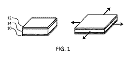
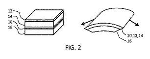
EAP装置の動作例として、図1及び図2に、EAPに基づく装置の可能な2つの動作モードを示す。この装置は、電極10と電極12との間に挟まれたEAP層14を備え、電極10と電極12は、EAP層14の互いに反対側の面にある。図1では、EAP層が自由に運動可能であるが、図2では、EAP層全体及びその電極が、一方の層側において支持キャリヤ(carrier)層16にクランプされている。図示されているようにEAP層を全方向に膨張させるためには、電極10と電極12とにわたって印加された電圧差(駆動信号)を使用して、EAP層の全体にわたる電場を提供する。図1では、自由に動くようにEAP層が取り付けられているため、これによってEAP層は変形するが、図2の同じ作動では、クランプにより運動の自由が制限されているため、装置は曲がる。装置工学を使用すると、EAP層を作動させたとき、すなわち装置を駆動したときに、非常にさまざまな装置出力を引き出すことができる。したがって、図示されているような一軸を軸にした非対称な湾曲を得るために、例えば分子配向(膜の延伸)を適用して、一方向の運動を強制することができる。この一方向の膨張は、EAP層の非対称性若しくはキャリヤ層の特性の非対称性に起因するか、又はこれら両者の組合せに起因する。
As an operation example of the EAP device, FIGS. 1 and 2 show two possible operation modes of the EAP-based device. This device includes an
図1及び図2の装置のようなEAP又はOAPに基づく装置は通常、アナログ装置である。これは、駆動対出力応答曲線が連続曲線であることを意味する。したがって、ゼロ・レベル信号/ゼロ強度信号以外の任意の信号は作動出力を与える。しかしながら、これらの装置では、その作動した状態(以後、作動状態)を維持するのに絶え間なく駆動する必要がある。ある場合には、アクチュエータに駆動信号を絶え間なく送ることが望まれない。したがって、その作動状態に留まるために駆動信号を絶え間なく加える必要のない装置が求められている。 Devices based on EAP or OAP, such as the devices in FIGS. 1 and 2, are usually analog devices. This means that the drive vs. output response curve is a continuous curve. Therefore, any signal other than the zero level signal / zero intensity signal gives an working output. However, these devices need to be continuously driven to maintain their working state (hereafter referred to as working state). In some cases, it is not desirable to continuously send drive signals to the actuator. Therefore, there is a need for a device that does not require constant application of drive signals to stay in that operating state.
本発明の目的は、上で説明したタイプの作動装置であって、その作動状態に留まるために駆動信号を絶え間なく加える必要のない作動装置を提供することにある。 An object of the present invention is to provide an actuating device of the type described above, which does not require a constant application of drive signals to remain in that actuated state.
この目的は、独立請求項によって定義された装置によって少なくとも部分的に達成される。従属請求項は有利な実施形態を提供する。 This objective is at least partially achieved by the equipment defined by the independent claims. Dependent claims provide an advantageous embodiment.
本発明によれば、
− キャリヤとキャリヤに取り付けられた活性材料(20)とを含む作動構造体(62)であって、活性材料の駆動に応答して少なくともキャリヤの曲がり及び/又は曲がりの変化を引き起こす作動構造体(62)と、
− 少なくとも作動構造体の第1の安定機械的状態と第1の安定機械的状態とは異なる第2の安定機械的状態を、第1の安定機械的状態と第2の安定機械的状態とのうちの少なくとも一方の安定機械的状態の曲げられた形状に作動構造体を機械的に拘束することによって規定する機械構造体(24)と
を備え、
− 活性材料を駆動すると、作動構造体が、第1の安定機械的状態から第2の安定機械的状態に切り換わることができる
装置が提供される。
According to the present invention
-A working structure (62) comprising a carrier and an active material (20) attached to the carrier, which causes at least bending and / or bending change of the carrier in response to driving of the active material ( 62) and
-At least the first stable mechanical state of the working structure and the second stable mechanical state different from the first stable mechanical state are defined as the first stable mechanical state and the second stable mechanical state. Provided with a mechanical structure (24) defined by mechanically constraining the working structure to the bent shape of at least one of them in a stable mechanical state.
− Provided is a device capable of switching the working structure from a first stable mechanical state to a second stable mechanical state when the active material is driven.
活性材料は、駆動されたときに変形することができる材料、又は駆動されたときにその形状を変化させることができる材料である。駆動は、例えば(電圧、電場若しくは電流を用いた)電気的な駆動、又は(ある周波数、色及び/若しくは強度の光学信号を用いた)光学的な駆動を意味しうる。 An active material is a material that can be deformed when driven, or a material that can change its shape when driven. Drive can mean, for example, electrical drive (using a voltage, electric field or current) or optical drive (using an optical signal of a certain frequency, color and / or intensity).
作動構造体は、作動構造体が曲げアクチュエータを提供するような態様で活性材料に取り付けられたキャリヤを含む。したがって、駆動は、作動構造体を曲げるか、又は作動構造体の曲がりを小さくする。 The working structure includes a carrier attached to the active material in such a manner that the working structure provides a bending actuator. Therefore, the drive bends the working structure or reduces the bending of the working structure.
機械構造体は、少なくとも2つの異なる安定機械的状態をアクチュエータがとることができるような態様で、アクチュエータを機械的に拘束する。 The mechanical structure mechanically constrains the actuator in such a manner that the actuator can take at least two different stable mechanical states.
安定機械的状態は、特に駆動などの外部刺激を装置に加えなくても維持されうる機械的状態、又は外部刺激を装置に加えなくても維持される機械的状態を意味する。したがって、機械構造体は、駆動を止めたときに少なくとも1つの安定機械的状態を維持するためのものである。作動構造体は、機械構造体と相互作用して、一方の状態からもう一方の状態へ切り換わるように装置を活性化する。このことは、装置が、切り換えられるときにだけ駆動を必要とし、安定状態にあるときには駆動を必要としないことを意味する。 The stable mechanical state means a mechanical state that can be maintained without applying an external stimulus such as driving to the device, or a mechanical state that can be maintained without applying an external stimulus to the device. Therefore, the mechanical structure is for maintaining at least one stable mechanical state when the drive is stopped. The working structure interacts with the mechanical structure to activate the device to switch from one state to the other. This means that the device needs to be driven only when it is switched and not when it is in a stable state.
第1の安定機械的状態は、作動構造体の駆動されていない平衡状態又は静止状態とすることができる。 The first stable mechanical state can be an undriven equilibrium or rest state of the working structure.
この装置は、作動構造体を機械構造体と組み合わせて、装置を作動させることができるようにし、また、装置が多数の安定状態を有することができるようにする。作動構造体のキャリヤ部分は機械構造体の部分であり、このことは装置を特にコンパクトにする。このデザインは、それ自体は双安定振舞いを提供しない、単純で平らな曲げアクチュエータ(少なくとも1つのアクチュエータ材料層及び少なくとも1つのキャリヤ層を備える多層)を可能にし、この曲げアクチュエータは、普通は平らな状態で生産され、その後、双安定作動振舞いをする装置に組み込まれる。 The device combines the working structure with the mechanical structure to allow the device to operate and also allows the device to have a number of stable states. The carrier portion of the working structure is the portion of the mechanical structure, which makes the device particularly compact. This design allows for a simple, flat bending actuator (multilayer with at least one actuator material layer and at least one carrier layer) that does not provide bistable behavior by itself, and this bending actuator is usually flat. It is produced in a state and then incorporated into a device that behaves in a bistable manner.
したがって、この装置を使用して、(しきい値よりも低いと効果がなく、しきい値よりも高いと一定の大きさの効果がある)ディジタル出力を与えることができ、又はさらには多レベル出力を与えることができる。したがって、本質的にアナログ式の作動構造体の作動がディジタル出力に変換される。このようにすると、アナログ駆動信号がディジタル作動出力に変換され、加えられた駆動信号が除去された後も作動状態が続く。 Therefore, this device can be used to provide digital output (below the threshold has no effect, above the threshold has a certain magnitude of effect), or even multi-level. Output can be given. Therefore, the operation of the essentially analog actuating structure is converted to digital output. In this way, the analog drive signal is converted to a digital actuation output, and the operating state continues even after the applied drive signal is removed.
この装置は、少なくとも第2の安定機械的状態に基づく作動出力又は少なくとも第2の安定機械的状態によって規定される作動出力を提供する作動装置であることが好ましい。この作動出力は、例えばストローク、力、歪み、圧力又は変位など、任意の種類の機械的出力を含みうる。変位は、1つ若しくは複数の軸に沿った1つ若しくは複数の方向の、又は1つ若しくは複数の点における、又は1つ若しくは複数の軸を軸にした、或いは上記の任意の1つの組合せによる、滑り、回転、曲げ
、よじれ、又は膨張に基づきうる。これは、作動構造体及び/又は機械構造体の特定のデザインの必要性に従ってデザインすることができる。
The device is preferably an actuator that provides an operating output based on at least a second stable mechanical state or an operating output defined by at least a second stable mechanical state. This working output may include any type of mechanical output, such as stroke, force, strain, pressure or displacement. Displacement is in one or more directions along one or more axes, or at one or more points, or about one or more axes, or by any combination of the above. Can be based on slip, rotation, bending, kinking, or swelling. It can be designed according to the specific design needs of the working and / or mechanical structures.
作動出力を提供するように作動構造体を配置することができる。その代わりに又はそれに加えて、作動出力を提供するために作動構造体及び/又は機械構造体と機械的に(接触して又は作用する力によって)相互作用する作動出力部材(例えばピストン、ロッド又は他の部材)が存在してもよい。 The working structure can be arranged to provide working power. Instead or in addition, an actuating output member (eg, a piston, rod or) that mechanically (by contacting or acting force) interacts with the actuating structure and / or the mechanical structure to provide the working power Other members) may be present.
一例では、機械的な力を外部から装置に加えることによって、装置がリセットされる。次いで、駆動すると、一方向にだけ、すなわち第1の安定状態から第2の安定状態に状態が切り換わる。 In one example, the device is reset by applying a mechanical force to the device from the outside. Then, when driven, the state is switched in only one direction, that is, from the first stable state to the second stable state.
本発明の装置はさらに、
− キャリヤが、第1の面及び第1の面の反対側の第2の面を有し、活性材料が第1の面に取り付けられていること、並びに
− アクチュエータ構造体が、第2の面に取り付けられた追加の活性材料を含み、この追加の活性材料は、この追加の活性材料の追加の駆動に応答して作動構造体の曲がり及び/又は曲がりの変化を引き起こすためのものであり、その結果、この追加の駆動時に、作動構造体は、第2の安定機械的状態から第1の安定機械的状態に切り換わることができること
を含むことができる。
The apparatus of the present invention further
-The carrier has a first surface and a second surface opposite the first surface, the active material is attached to the first surface, and-the actuator structure is the second surface. Including an additional active material attached to, this additional active material is intended to cause bending and / or bending change of the working structure in response to additional driving of this additional active material. As a result, during this additional drive, the working structure can include being able to switch from a second stable mechanical state to a first stable mechanical state.
したがって、この追加の駆動を止めても、機械構造体は、第1の安定機械的状態を維持することができる。したがって、この装置は、2つの安定状態間で駆動可能であり、同時に、デザインコンパクト性が維持される。 Therefore, even if this additional drive is stopped, the mechanical structure can maintain the first stable mechanical state. Therefore, the device can be driven between two stable states, while maintaining design compactness.
活性材料と追加の活性材料とは同じであっても、異なってもよい。両方の材料を電気活性材料とすることができ、又は両方の材料を光学活性材料とすることができる。或いは、一方の材料を電気活性材料とし、もう一方の材料を光学活性材料とすることもできる。 The active material and the additional active material may be the same or different. Both materials can be electroactive materials, or both materials can be optically active materials. Alternatively, one material can be an electrically active material and the other material can be an optically active material.
基板及び任意の活性材料は、層スタックとして配置されていることが好ましい。活性材料、追加の活性材料、機械構造体のキャリヤ部分、及び任意選択の他の部分は、互いの上に積み重ねられた層形態で製作することができる。任意選択の部分は、1つ若しくは複数の電極(電気活性材料)又は1つ若しくは複数の光学ガイド/光ガイド(光学活性材料)など、駆動を提供するための部分とすることができる。これは、都合のよいデザインである。 The substrate and any active material are preferably arranged as a layer stack. The active material, additional active material, carrier portion of the mechanical structure, and optional other portions can be made in the form of layers stacked on top of each other. The optional portion can be a portion for providing drive, such as one or more electrodes (electroactive material) or one or more optical guides / optical guides (optically active material). This is a convenient design.
本発明では、第1の機械的状態及び第2の機械的状態の両方の機械的状態において、アクチュエータを、曲げられた形状に機械的に拘束することができる。したがって、機械的に拘束されたアクチュエータ及び特にキャリヤを、この拘束による(例えば、ばねとして振る舞う)双安定部分とすることができる。この部分は層の形状を有することができる。この部分又は層は例えば、切換え中に2つの安定状態間で素早く切り換わる。例えば、この部分又は層は、凸形状態と凹形状態との間で、又は、それと等価に上方へ突き出た状態と下方へ突き出た状態との間で切り換わる。したがって、第1の安定機械的状態の曲げられた形状は、第2の安定機械的状態の曲げられた形状とは反対の形状にできる。 In the present invention, the actuator can be mechanically constrained to a bent shape in both the first mechanical state and the second mechanical state. Thus, mechanically constrained actuators and especially carriers can be bistable portions due to this restraint (eg, behaving as springs). This portion can have the shape of a layer. This portion or layer switches quickly between two stable states, for example, during switching. For example, this portion or layer switches between a convex state and a concave state, or equivalently between an upwardly protruding state and a downwardly protruding state. Therefore, the bent shape of the first stable mechanical state can be the opposite of the bent shape of the second stable mechanical state.
或いは、駆動されていない状況において、機械的に拘束されていない第1の安定機械的状態又は機械的に拘束されていない第2の安定機械的状態にあるときに、作動構造体を実質的に平らにすることもでき、もう一方の状態は依然として曲げられた形状である。 Alternatively, in an undriven situation, when in a first stable mechanical state that is not mechanically constrained or a second stable mechanical state that is not mechanically constrained, the working structure is substantially. It can also be flattened, the other state is still in a bent shape.
装置は、ハウジングを備えることができ、機械構造体がハウジングの蓋を形成し、作動構造体がハウジング内にある。これは、上蓋が装置の機械的作動出力を提供する、閉じた自足式のデザインを提供する。 The device can include a housing, the mechanical structure forms the lid of the housing, and the working structure is within the housing. It provides a closed, self-sufficient design in which the top lid provides the mechanical working output of the device.
このコンパクトなデザインは、追加の作動構造体を有する装置にとって有利である。これは、多数の構造体(層の形態をとることがある)を含む場合であっても、コンパクトな装置が、双方向切換え能力及び安定性を備えることができるためである。 This compact design is advantageous for devices with additional working structures. This is because a compact device can provide bidirectional switching capability and stability, even when it contains a large number of structures (which may take the form of layers).
活性材料及び/又は追加の活性材料は、キャリヤのエリアの一部分だけ、例えばエッジ部分だけにわたって広がることができる。この材料は、作動構造体がその状態を切り換えるのに十分なものでありさえすればよい。 The active material and / or additional active material can spread over only a portion of the carrier area, eg, the edge portion. This material need only be sufficient for the working structure to switch its state.
機械構造体は、作動構造体を安定機械的状態でその位置に保持することができる複数の保持位置を有する保持装置を備えることができ、それぞれの保持位置は異なるアクチュエータ位置に対応し、これらの保持位置のうちの少なくとも1つの保持位置が、第1の安定機械的状態と第2の安定機械的状態とのうちの少なくとも一方の安定機械的状態の曲げられた形状に作動構造体を機械的に拘束する。 The mechanical structure can include holding devices having a plurality of holding positions capable of holding the working structure in that position in a stable mechanical state, each holding position corresponding to a different actuator position and these. At least one of the holding positions mechanically moves the working structure into a bent shape in at least one of the first stable mechanical state and the second stable mechanical state. Restrained to.
作動構造体が駆動された後に作動構造体を保持することによって、駆動が終わった後も作動構造体の形状は少なくとも部分的に保持される。保持装置は例えば、作動構造体の固定されたエッジから異なる距離のところに作動構造体の移動可能なエッジを保持するための装置であり、複数の保持切欠きを備える。 By holding the working structure after it has been driven, the shape of the working structure is at least partially retained after the driving is finished. The holding device is, for example, a device for holding the movable edge of the working structure at different distances from the fixed edge of the working structure and includes a plurality of holding notches.
電気活性高分子を電気活性材料として使用する装置は、電場駆動性材料とイオン駆動性材料とにさらに区分することができる。電場駆動性EAPは、電気機械的な直接結合を介して電場によって作動する。電場駆動性EAPは普通、高い電場(ボルト/m)であるが低い電流を必要とする。駆動電圧をできるだけ低く保つため、高分子層は通例は薄い。イオン性(ionic)EAPは、イオン及び/又は溶媒の電気的に誘起された輸送によって活性化される。イオン性EAPは普通、低電圧であるが高電流を必要とする。イオン性EAPは、液体/ゲル電解質媒質を必要とする(ただしいくつかの材料システムは固体電解質を使用して動作することもできる)。これらの分類のEAPはともに多くの種類を有し、それらはそれぞれ、独自の利点及び欠点を有する。 Devices that use an electroactive polymer as an electroactive material can be further classified into an electric field driven material and an ion driven material. The electric field drive EAP is operated by an electric field via an electromechanical direct coupling. Electric field drive EAP usually has a high electric field (volts / m) but requires a low current. The polymer layer is usually thin to keep the drive voltage as low as possible. Ionic EAP is activated by electrically induced transport of ions and / or solvent. Ionic EAP usually has a low voltage but requires a high current. Ionic EAP requires a liquid / gel electrolyte medium (although some material systems can also operate with solid electrolytes). Both of these categories of EAPs have many varieties, each with its own advantages and disadvantages.
電場駆動性EAPの例は、圧電高分子(Piezoelectric polymer)、電気歪み高分子(Electrostrictive polymer)(例えばPVDFベースのリラクサー高分子(relaxor polymer)又はポリウレタン)及び誘電エラストマー(Dielectric Elastomer)を含む。他の例は、電気歪みグラフト重合体(Electrostrictive Graft polymer)、電気歪み紙(Electrostrictive paper)、エレクトレット(Electret)、電気粘弾性エラストマー(Electroviscoelastic Elastomer)及び液晶エラストマー(Liquid Crystal Elastomer)を含む。 Examples of electric field driven polymers include Piezoelectric polymers, Electrolytic polymers (eg PVDF-based relaxor polymers or polyurethanes) and Dielectric Elastomers. Other examples include electrostrained graft polymers (Electretribive Graft polymer), electrostrained paper (Electrettive paper), electrets, electroviscoelastic elastomers (Electretographic Elastomers) and liquid crystal elastomers (Liquid crystal elastomers).
イオン駆動性EAPの例は、共役/導電性高分子、イオン性高分子金属複合体(Ionic Polymer Metal Composite:IPMC)及びカーボン・ナノチューブ(CNT)である。他の例はイオン性高分子ゲルを含む。 Examples of ion-driven EAPs are conjugated / conductive polymers, ionic polymer metal composites (IPMCs) and carbon nanotubes (CNTs). Other examples include ionic polymeric gels.
光学活性材料は、照射されるとシス−トランス異性化を受けうる1つ又は複数の二重結合を有する高分子を含むことができる。このような結合はC=C、N=C又はN=N結合でありうる。このような材料は例えばスチルベンを含むことができる。 The optically active material can include macromolecules with one or more double bonds that can undergo cis-trans isomerization when irradiated. Such a bond can be a C = C, N = C or N = N bond. Such materials can include, for example, stilbene.
ある種の用途では、例えば位置決めシステム及び制御されたトポロジ表面において、アクチュエータのアレイが役立つことがある。しかしながら、アクチュエータの駆動電圧はかなり高い(50V超)ため、それぞれのアクチュエータをそれ自体のドライバ集積回路を用いて個別に駆動することはコスト高に直結する。 In certain applications, an array of actuators may be useful, for example in positioning systems and controlled topology surfaces. However, since the drive voltage of the actuators is quite high (more than 50 V), driving each actuator individually using its own driver integrated circuit is directly linked to high cost.
パッシブ・マトリックス・アレイは、行(n個の行)接続及び列(m個の列)接続だけを使用するアレイ駆動システムの単純な実施態様であり、アクティブ・マトリックス・アレイよりも低コストであり、アクティブ・マトリックス・アレイほど複雑でない。最大(n×m)個のアクチュエータをアドレス指定するのに必要なドライバは(n+m)個だけであるため、この手法は、はるかに費用効果に優れた手法であり、さらに追加配線のコスト及び空間を節約する。 A passive matrix array is a simple embodiment of an array drive system that uses only row (n row) and column (m column) connections and is less costly than an active matrix array. , Not as complicated as the active matrix array. This method is much more cost effective, as only (n + m) drivers are required to address the maximum (n × m) actuators, and the cost and space of additional wiring. To save.
理想的には、パッシブ・マトリックス装置では、それぞれの個々のアクチュエータを、隣接するアクチュエータに影響を与えることなく、その最大電圧まで作動させるべきである。しかしながら、(電圧しきい値を使用しない)伝統的なEAP装置では、隣接するアクチュエータへのクロストークがある程度存在する。1つのアクチュエータを作動させるために電圧を印加すると、その周囲のアクチュエータも電圧を感受し、部分的に作動する。多くの用途にとってこれは不要な効果である。 Ideally, in a passive matrix device, each individual actuator should operate to its maximum voltage without affecting adjacent actuators. However, in traditional EAP devices (which do not use voltage thresholds), there is some crosstalk to adjacent actuators. When a voltage is applied to operate one actuator, the actuators around it also sense the voltage and partially operate. This is an unnecessary effect for many applications.
この状況が、米国特許第8,552,846号明細書に記載されている。この文献は、しきい電圧又は双安定を使用しないEAP装置のパッシブ・マトリックス駆動を検討している。この文献は、2レベル駆動方式用のパッシブ・マトリックス手法を開示している。この手法は、最良で3:1の作動電圧コントラスト比を提供し(すなわち「作動していない」アクチュエータは最大作動電圧の33%の作動を示し)、そのため、真の双安定振舞いを可能にしない。作動コントラスト比3:1は圧力レベル比9:1と等価であることに留意されたい(圧力レベルは電圧の2乗に比例するため)。しかしながら、このシステムは2レベル駆動だけに対応している。第3の駆動レベルを使用すると、作動していないEAP装置の作動レベルが変動することになる。 This situation is described in US Pat. No. 8,552,846. This document considers passive matrix drive of EAP devices that do not use threshold voltage or bistable. This document discloses a passive matrix method for a two-level drive scheme. This technique provides a working voltage contrast ratio of at best 3: 1 (ie, "non-working" actuators show 33% of maximum working voltage working) and therefore does not allow true bistable behavior. .. Note that the working contrast ratio 3: 1 is equivalent to the pressure level ratio 9: 1 (because the pressure level is proportional to the square of the voltage). However, this system only supports two-level drive. Using the third drive level will cause the operating level of the non-operating EAP device to fluctuate.
したがって、特にEAP装置、及び作動装置一般を、アドレス指定されるアレイ、特にパッシブ・マトリックス・アレイ内で使用することには限界がある。 Therefore, there is a limit to the use of EAP devices in general, and actuators in general, in addressed arrays, especially passive matrix arrays.
本発明の態様に基づく例によれば、本発明によって定義された複数の装置を備えるシステムが提供される。これらの複数の装置は、アレイの列及び行に配置されることが好ましい。このシステム又は装置のアレイは多安定装置を利用する。このようにすると記憶機能が可能になり、その結果、複数の装置又は装置のアレイ上に所望のマトリックス・アドレス指定パターンを書き込み、記憶することができるようになる。 According to an example based on an aspect of the present invention, a system including a plurality of devices defined by the present invention is provided. These plurality of devices are preferably arranged in columns and rows of the array. This system or device array utilizes a multi-stabilizer. In this way, a storage function becomes possible, and as a result, a desired matrix addressing pattern can be written and stored on a plurality of devices or an array of devices.
駆動信号を装置に提供するため、これらの複数の装置をそれぞれ、少なくとも1本の信号線に接続することができる。光学的に作動させる装置又は光学的に駆動される装置では、このような信号線を光ガイドとすることができる。電気的に駆動される装置では、このような信号線を電極とすることができる。好ましくは、それぞれの装置が、第1の信号線及び第2の信号線に接続される。一方の信号線は、駆動信号を提供するための線であり、もう一方の信号線は、選択信号を提供するための線である。こうすることは、マトリックス・アレイとして配列された複数の装置にとって有用である。 Since the drive signal is provided to the device, each of these devices can be connected to at least one signal line. In an optically actuated device or an optically driven device, such a signal line can be used as an optical guide. In electrically driven devices, such signal lines can be used as electrodes. Preferably, each device is connected to a first signal line and a second signal line. One signal line is a line for providing a drive signal, and the other signal line is a line for providing a selection signal. This is useful for multiple devices arranged as a matrix array.
好ましくは、これらの装置を、パッシブ・マトリックス・アドレス指定方式のドライバ装置に接続することができる。より具体的には、これらの複数のそれぞれの装置が、活性材料として電気活性材料を含み、駆動信号を装置に提供する第1の信号線及び第2の信号線に接続されており、このシステムがさらに、少なくとも2つの可能な信号レベルを第1の信号線に提供し、少なくとも2つの可能な信号レベル第2の信号線に提供するドライバ装置を備え、これらの信号が、装置によって受け取られる駆動信号が、第1の信号線の1つの信号レベルと第2の信号線の1つの信号レベルとの組合せであるような態様で提供され、組み合わされた4つの可能な信号レベルのうちの1つの信号レベルだけが、装置の第1の安定状態から第2の安定状態への切換えを提供する。 Preferably, these devices can be connected to a passive matrix addressing driver device. More specifically, each of these plurality of devices contains an electroactive material as an active material and is connected to a first signal line and a second signal line that provide a drive signal to the device, and this system. Further comprises a driver device that provides at least two possible signal levels to the first signal line and at least two possible signal levels to the second signal line, the drive by which these signals are received by the device. The signal is provided in such a manner that it is a combination of one signal level of the first signal line and one signal level of the second signal line, and is one of four possible signal levels combined. Only the signal level provides the switching from the first stable state of the device to the second stable state.
多レベル駆動方式に、組み合わされた5つ以上の信号レベルが存在してもよいことに留意されたい。しかしながら、第1の信号線の最小信号レベル及び最大信号レベルと第2の信号線の最小信号レベル及び最大信号レベルとの組合せの結果である、このような組み合わされたレベルが少なくとも4つ存在する。 Note that there may be five or more combined signal levels in a multi-level drive scheme. However, there are at least four such combined levels that are the result of the combination of the minimum and maximum signal levels of the first signal line and the minimum and maximum signal levels of the second signal line. ..
好ましくは、それぞれの装置について、
駆動信号は、第1のしきい値Vbiよりも低い組み合わされた信号レベルを有し、第1の安定状態から第2の安定状態に向かう作動を提供するが、駆動信号が除去されると第1の安定状態に戻り、
駆動信号は、第2のしきい値よりも高い組み合わされた信号レベルを有し、第1の安定状態から第2の安定状態への作動を提供し、駆動信号が除去されても第1の安定状態には戻らず、第2のしきい値は、第1のしきい値Vbiの大きさよりも大きな第1のマージンVdrである大きさを有する。
Preferably, for each device
The drive signal has a combined signal level lower than the first threshold value Vbi and provides an operation from the first stable state to the second stable state, but when the drive signal is removed, the first Return to the stable state of 1,
The drive signal has a combined signal level higher than the second threshold and provides operation from the first stable state to the second stable state, even if the drive signal is removed. It does not return to the stable state, and the second threshold has a magnitude of the first margin Vdr, which is larger than the magnitude of the first threshold Vbi.
したがって、個々の装置に安定状態を切り換えさせるのには不十分な駆動信号の範囲と、それによって装置が状態を一方の安定状態からもう一方の安定状態へ切り換える別の範囲とが存在する。この特性を使用して、逐次駆動方式中の装置間のクロストークを防ぐことができる。クロストークが起こると、以前に記憶された作動状態が失われる結果となる。このことは、複数の装置をアドレス指定するパッシブ・マトリックス型のアドレス指定にとって最も都合がよい。 Therefore, there is a range of drive signals that is insufficient for individual devices to switch between stable states, and another range that allows the device to switch states from one stable state to the other. This characteristic can be used to prevent crosstalk between devices during the sequential drive system. Crosstalk results in the loss of previously remembered operating states. This is most convenient for passive matrix addressing, which addresses multiple devices.
このシステムでは、第1の信号線及び第2の信号線のうちの一方の信号線については、2つの可能な信号レベルがゼロ及び第1のしきい値Vbiの大きさであり、第1の信号線及び第2の信号線のうちのもう一方の信号線については、2つの可能な信号レベルがゼロ及び第1のマージンVdrの大きさであり、これらの非ゼロ信号レベルの極性が反対であるような態様の信号レベルを提供するように、ドライバを配置することができる。 In this system, for one of the first and second signal lines, the two possible signal levels are zero and the magnitude of the first threshold Vbi, the first. For the signal line and the other signal line of the second signal line, the two possible signal levels are the magnitudes of zero and the first margin Vdr, and the polarities of these non-zero signal levels are opposite. The driver can be arranged to provide some aspect of the signal level.
このようにすると、作動状態の変化を引き起こすのに十分なのは、これらの非ゼロ・レベル信号間の差だけである(一方が正、もう一方が負であるため、この差はそれぞれの信号レベル(及びそれとともに個々の駆動信号)よりも大きい)。 In this way, it is only the difference between these nonzero level signals that is sufficient to cause a change in operating state (because one is positive and the other is negative, this difference is the respective signal level ( And along with the individual drive signals)).
第1のしきい値Vbiの大きさは、第1のマージンVdrの大きさよりも大きいことが好ましい。例えば、第1のしきい値Vbiの大きさは、第1のマージンVdrの大きさの少なくとも5倍とすることができる。第1のマージンVdrが小さいほど、より急激に装置の双安定振舞いが起こり、したがって、必要な駆動電圧の大きさは小さくなる。 The magnitude of the first threshold value Vbi is preferably larger than the magnitude of the first margin Vdr. For example, the magnitude of the first threshold value Vbi can be at least five times the magnitude of the first margin Vdr. The smaller the first margin Vdr, the more rapidly the bistable behavior of the device occurs, and therefore the smaller the magnitude of the required drive voltage.
この装置のアレイでは、機械的リセットの形態の外部入力を受け取るように装置を適合させることができる。これは例えば圧力信号を含む。 The array of devices can be adapted to receive external inputs in the form of mechanical resets. This includes, for example, a pressure signal.
或いは、それぞれの装置について、
第3のしきい値Vresよりも高い組み合わされた駆動レベルを有するリセット駆動信号は、この駆動信号が除去されたときに第1の状態へのリセットを提供する。
Alternatively, for each device
A reset drive signal having a combined drive level higher than the third threshold Vres provides a reset to the first state when this drive signal is removed.
このリセット駆動信号は、装置の機械的リセットではなく、装置の電気的リセットを可能にする。次いで、第1及び第2の信号線上に提供される信号は一緒に、リセット駆動信号を同時に、又は行ごと若しくは列ごとに装置に提供するように適合される。 This reset drive signal allows an electrical reset of the device rather than a mechanical reset of the device. The signals provided on the first and second signal lines are then adapted together to provide the reset drive signal to the device simultaneously, row by row or column by column.
このシステムでは、装置が、活性材料として電気活性高分子を含むアクチュエータ装置であることが好ましい。 In this system, the device is preferably an actuator device containing an electroactive polymer as an active material.
本発明の別の態様に基づく例は、本発明に基づく複数の装置を動作させる方法を提供する。この方法では、これらの複数のそれぞれの装置が、活性材料として電気活性材料を含み、駆動信号を装置に提供する第1の信号線及び第2の信号線に接続されており、この方法は、少なくとも2つの可能な信号レベルを第1の信号線に提供し、少なくとも2つの可能な信号レベルを第2の信号線に提供するステップを有し、これらの信号は、装置によって受け取られる駆動信号が、第1の信号線の1つの信号レベルと第2の信号線の1つの信号レベルとの組合せであるような態様で提供され、組み合わされた4つの可能な信号レベルのうちの1つの信号レベルだけが、装置の第1の安定状態から第2の安定状態への切換えを提供する。 An example based on another aspect of the invention provides a method of operating a plurality of devices according to the invention. In this method, each of these plurality of devices contains an electroactive material as an active material and is connected to a first signal line and a second signal line that provide a drive signal to the device. It has a step of providing at least two possible signal levels to the first signal line and at least two possible signal levels to the second signal line, these signals being the drive signal received by the device. , One signal level of one of the four possible signal levels provided and combined in such a manner as a combination of one signal level of the first signal line and one signal level of the second signal line. Only provides the switching from the first stable state of the device to the second stable state.
それぞれの装置について、
第1のしきい値Vbiよりも低い組み合わされた信号レベルを有する駆動信号は、第1の安定状態から第2の安定状態に向かう作動を提供することができるが、駆動信号が除去されると第1の安定状態に戻り、
第2のしきい値よりも高い組み合わされた信号レベルを有する駆動信号は、第1の安定状態から第2の安定状態への作動を提供することができ、駆動信号が除去されても第1の安定状態へは戻らず、第2のしきい値は、第1のしきい値Vbiの大きさよりも大きな第1のマージンVdrである大きさを有し、
この方法は、次いで、
2つの可能な信号レベルのうちの一方の信号レベルを、ゼロから及び第1のしきい値Vbiの大きさから選択された第1の信号線及び第2の信号線のうちの選択された信号線に加えるステップ、及び
2つの可能な信号レベルのうちの一方の信号レベルを、ゼロから及び第1のマージンVdrの大きさから選択された第1の信号線及び第2の信号線のうちの選択された信号線に加えるステップ
を有することができ、これらの非ゼロ信号レベルの極性は互いに反対の極性を持つ。
For each device
A drive signal having a combined signal level lower than the first threshold Vbi can provide an operation from the first stable state to the second stable state, but when the drive signal is removed. Returning to the first stable state,
A drive signal having a combined signal level higher than the second threshold can provide operation from a first stable state to a second stable state, even if the drive signal is removed. The second threshold has a magnitude of a first margin Vdr that is greater than the magnitude of the first threshold Vbi, without returning to the stable state of.
This method then
A selected signal of a first signal line and a second signal line selected from zero and the magnitude of the first threshold Vbi for one of the two possible signal levels. The step of adding to the line, and the signal level of one of the two possible signal levels, of the first and second signal lines selected from zero and from the magnitude of the first margin Vdr. It can have steps to add to the selected signal line, and the polarities of these non-zero signal levels have opposite polarities.
次に、添付図面を参照して本発明の例を詳細に説明する。 Next, an example of the present invention will be described in detail with reference to the accompanying drawings.
図1及び図2の装置については本出願の導入部分で説明した。図2の装置は、活性材料としての電気活性高分子EAPに基づく第1の例である。活性材料はキャリヤに取り付けられている。 The devices of FIGS. 1 and 2 have been described in the introductory part of this application. The device of FIG. 2 is a first example based on an electroactive polymer EAP as an active material. The active material is attached to the carrier.
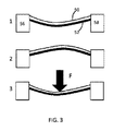
図3は、基板シート(キャリヤ)50が、EAPを含む作動材料52に結合され、その結果、双安定装置が基板と組み合わされて(接合されて)EAPを構成した、EAPに基づく第1の装置を示す。この装置は、図2を参照して説明したアクチュエータ構造体を構成する。したがって、EAPの駆動を実行するための駆動信号を受け取ることができる電極装置が存在する。この駆動によってこの構造体は曲がる。この基板又はキャリヤは機械構造体の部分であり、機械構造体はさらに部分56及び58を含む。部分56と部分58との間で、アクチュエータは、駆動信号が加えられていないときでも基板(及びこの場合にはさらに作動構造体全体)がやや曲げられているような態様で、水平方向に拘束(クランプ又は固定)されている。EAPを作動させると、EAP−キャリヤ結合体は状態1から状態2に移る。切換えの後、作動駆動は止められ、EAP−基板結合体は状態2(誘電体装置では状態1)に留まる。したがって、作動構造体は状態2に維持される。基板のプレストレシング(prestressing)はそれ自体が必要ないことに留意されたい。このことは、部分56と部分58との間に作動構造体が拘束されていないときには、作動構造体が実質的に平らになりうることを意味する。したがって、製造が容易な通常の作動構造体を使用して、双安定でコンパクトな装置を生み出すことができる。単一のEAPの使用は、装置をその初期状態にリセットするのに外力が必要であることを意味する。図3の状態3を参照されたい。矢印は加えられた外力を示している。この装置は、ユーザ・インタフェース(UI)上のボタンなどの対話装置において有用であり得る。
FIG. 3 shows the first EAP-based, in which the substrate sheet (carrier) 50 is coupled to the working
したがって、この作動構造体は、凹形形状と凸形形状との間で切り換わる。以下で使用される用語「上」及び「下」、「上へ」及び「下へ」又は「上方へ」及び「下方へ」は、この形状の切換えに基づいて理解されるべきであり、単に相対的な状態を表す。 Therefore, this working structure switches between a concave shape and a convex shape. The terms "up" and "down", "up" and "down" or "up" and "down" used below should be understood on the basis of this shape switching and are simply Represents a relative state.
部分56及び58は、取付具の部分又はフレームの部分とすることができる。この取付具又はフレームは、より大きな装置のハウジング内に存在することがあり、又はより大きな装置のハウジングの部分であることがある。
The
図4は、図3のシステムの変更を示し、この変更では、双安定機械シート60が2つの作動層62(EAP1を含む)及び64(EAP2を含む)に結合されており(取り付けられており)、その結果、この双安定装置は、2つのEAPを、固定端56と固定端58との間にクランプされた座屈ディスク(buckling disk)又は基板と一体の部分として含む。2つのEAPの使用は、駆動を使用した可逆装置が可能になることを意味する。要するに、この装置は、(EAP62を含む)第1の作動構造体と(EAP64を含む)第2の作動構造体とを含み、第1の作動構造体と第2の作動構造体とがキャリヤ60を共有する。
FIG. 4 shows a modification of the system of FIG. 3, in which the bistable
この装置は、図3の装置と同じように機能するが、外力又は圧力ラインの代わりに別の駆動信号を使用してディスクを元の状態にリセットするために、追加の作動材料が使用される。駆動装置への接続及び駆動を実行することができる。したがって、このような装置は、2つの駆動信号入力、すなわち作動構造体用の1つの駆動信号入力及び追加の作動構造体用の1つの駆動信号入力を有しうる。この場合、これらの構造体はともに、ドライバ装置を使用して電気的に駆動される。したがって、これらの構造体はそれぞれ、EAP層の各面に1つずつ、合わせて2つの電極を備える。電極への入力リード線を減らすため、作動構造体の1つの電極と追加の作動構造体の1つの電極とは電気的に接続されている。それらの電極を同じ電圧、好ましくはゼロ・ボルト/大地電位に保つことができる。次いで、2つの入力電極だけ、すなわち作動構造体の1つの電極及び追加の作動構造体の1つの電極だけを使用して、残りの2つの電極に電圧をかけることができる。共通の電極と残りの電極のうちの一方の電極との間に電圧差を生じさせると、作動構造体又は追加の作動構造体が作動する。活性材料が異なる場合には、駆動の自由度をより大きくするために、接続された電極を分離することができる。しかしながら、そのためにはより複雑なドライバが必要となる。 This device functions in the same way as the device in FIG. 3, but additional working material is used to reset the disk to its original state using another drive signal instead of an external force or pressure line. .. It can connect to and drive the drive. Thus, such a device may have two drive signal inputs, one drive signal input for the working structure and one drive signal input for the additional working structure. In this case, both of these structures are electrically driven using a driver device. Therefore, each of these structures comprises two electrodes, one on each side of the EAP layer. In order to reduce the input leads to the electrodes, one electrode of the working structure and one electrode of the additional working structure are electrically connected. The electrodes can be kept at the same voltage, preferably zero volt / ground potential. Only two input electrodes, i.e. one electrode of the working structure and one electrode of the additional working structure, can be used to apply voltage to the remaining two electrodes. Creating a voltage difference between the common electrode and one of the remaining electrodes activates the working structure or additional working structure. If the active materials are different, the connected electrodes can be separated for greater freedom of drive. However, this requires a more complex driver.
図4は、アクチュエータを活性化させる際のさまざまなステップを示し、それらのステップは、EAPの活性化が必要なのは、1つの状態から別の状態へ切り換わる間だけであることを示す。得られる効果、すなわち座屈アクチュエータの運動は、2つの状態だけを有するディジタル効果である。EAPの作動中に状態の変化が起こる。 FIG. 4 shows the various steps in activating the actuator, which show that EAP activation is required only during the transition from one state to another. The effect obtained, i.e., the motion of the buckling actuator, is a digital effect with only two states. A change of state occurs during the operation of the EAP.
ステップ1では、装置は、下方へ変形した安定状態で開始し、EAP層は活性化されていない。
In
ステップ2には、上のEAP62だけを作動させて、上方へ変形した状態に状態を切り換えた様子が示されている。
In
ステップ3では、装置が、上方へ変形した安定状態のままである。EAP層は活性化されていない。
In
ステップ4では、下のEAP64だけを作動させることによって、下方へ変形した状態に状態が切り換わる。
In
図3及び図4では、機械的に双安定の層と電気活性高分子層とが一緒に接合されて、シート構造体を形成している。この接合は、接着剤又は他の取付け手段を使用することによって達成することができる。 In FIGS. 3 and 4, the bistable layer and the electroactive polymer layer are mechanically joined together to form a sheet structure. This joining can be achieved by using an adhesive or other mounting means.
アクチュエータがキャリヤを共有する図4の装置の代替装置として、それぞれが図3の形態を有する分離された2つのアクチュエータを使用し、次いで、それらの2つのアクチュエータを、互いに対して、キャリヤどうしが背中合わせになるような向きに配置することもできる。 As an alternative to the device of FIG. 4 in which the actuators share a carrier, two separate actuators, each having the form of FIG. 3, are used, and then the two actuators are placed back-to-back with each other. It can also be arranged so that it becomes.
図5は、図4の装置の変更を示し、この変更では、双安定機械シート(基板)70の縁の両面にEAP72、74が提供されている。
FIG. 5 shows a modification of the apparatus of FIG. 4, in which
この例は、2つのEAP層を使用することによって可逆的な効果を提供する同じ原理を使用するが、EAP層の長さは、座屈ディスクの表面の部分だけに限定されている。EAP層は、所望の機械的運動を引き起こすのに十分なものでありさえすればよい。 This example uses the same principle that provides a reversible effect by using two EAP layers, but the length of the EAP layer is limited to only the surface portion of the buckling disc. The EAP layer need only be sufficient to cause the desired mechanical motion.
このように、この電気活性高分子層は、機械的に双安定の層のエリアの一部分だけ、例えばエッジ部分だけにわたって広がっている。 Thus, the electroactive polymer layer mechanically extends over only a portion of the bistable layer area, eg, the edge portion.
図5は、装置の動作サイクルの4つのステップを示す。 FIG. 5 shows four steps of the operation cycle of the device.
ステップ1では、装置は、上方へ変形した安定状態で開始し、EAP層は活性化されていない。
In
ステップ2には、下のEAP74だけを作動させて、下方へ変形した状態に状態を切り換えた様子が示されている。
In
ステップ3では、装置が、下方へ変形した安定状態のままである。EAP層は活性化されていない。
In
ステップ4では、上のEAP72だけを作動させることによって、上方へ変形した状態に状態が切り換わる。
In
EAPの活性化が必要なのは、1つの安定状態から別の安定状態へ切り換わる間だけであり、それによって、EAPの活性化は、2つの状態だけを有するディジタル運動を座屈アクチュエータに提供する。EAPの作動中に状態の変化が起こる。 Activation of the EAP is required only during the transition from one stable state to another, so that activation of the EAP provides the buckling actuator with a digital motion having only two states. A change of state occurs during the operation of the EAP.
本発明のアクチュエータは、アクチュエータ材料とキャリヤとを交互に含む層スタックの形態をとることができる。後続のこれらの層は全て、互いに対して取り付けられていてもよい。したがって、図3又は図4のアクチュエータは実際に、多数の層50及び52又は多数の層60、62及び64を交互に含むことができる。
The actuator of the present invention can take the form of a layer stack containing alternating actuator materials and carriers. All of these subsequent layers may be attached to each other. Thus, the actuator of FIG. 3 or 4 can actually include
図5は、切換えの際に圧力を等しくするための通気孔を示している。 FIG. 5 shows vents for equalizing pressure during switching.
以上の例は、安定状態間で変形する機械構造体を利用する。この機械構造体は、EAP層の駆動信号が止められたときでもEAP層を変形した状態に維持するのに十分な堅さを有する。 The above example utilizes a mechanical structure that deforms between stable states. This mechanical structure is rigid enough to keep the EAP layer in a deformed state even when the drive signal of the EAP layer is stopped.
代替実施形態は、掛け金型構造体を使用することによって、駆動信号が除去された後もEAP層をある位置に保持するものである。例えば、機械構造体は、非駆動状態の電気活性高分子層をその位置に保持することができる複数の保持位置を有する保持装置を構成することができ、それらの保持位置はそれぞれ、異なるアクチュエータ位置に対応する。要するに、この状況は、以前の例の図3及び図4の固定端56及び58のうちの一方の固定端が、もう一方の固定端に対して多数の位置を有する状況に対応する。このようにすると、それぞれの保持位置が、準固定端によって規定される。 An alternative embodiment is to use a stake structure to hold the EAP layer in place even after the drive signal has been removed. For example, the mechanical structure can constitute a holding device having a plurality of holding positions capable of holding the non-driven electroactive polymer layer at that position, and the holding positions are different actuator positions. Corresponds to. In short, this situation corresponds to a situation in which one of the fixed ends 56 and 58 of FIGS. 3 and 4 of the previous example has a large number of positions with respect to the other fixed end. In this way, each holding position is defined by the semi-fixed end.
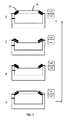
図6は、機械構造体が保持装置80を構成する例を示す。保持装置80は、非駆動状態の電気活性高分子層をその位置に保持することができる複数の保持位置80a、80b(この例では2つの保持位置が示されている)を有する。それらの保持位置はそれぞれ、異なるアクチュエータ位置に対応する。
FIG. 6 shows an example in which the mechanical structure constitutes the holding
図6(a)にはこの装置の平面図が示されている。図6(b)から図6(d)は、一方のアクチュエータ位置からもう一方のアクチュエータ位置へ駆動されている装置を示している。 FIG. 6A shows a plan view of this device. 6 (b) to 6 (d) show a device driven from one actuator position to the other actuator position.
EAP層82は、EAP部分とキャリヤとを備える2層構造体として示されているが、EAP層82は、上記の例とは違い、機械的に双安定の要素を含まない。双安定特性は保持装置80によって与えられる。
Although the
このEAP層は、支持体84によって示されている固定された第1のエッジ部分と移動可能な反対側のエッジ86とを有し、具体的には、エッジ86は、切欠き80a、80bのうちの一方の切欠きの中へ移動可能である。
This EAP layer has a fixed first edge portion indicated by a
一方の安定状態からもう一方の安定状態へ移行させるため、このEAP層の作動を使用して、EAP層のエッジ86を一方の切欠きの中へ移動させる。 This EAP layer operation is used to move the edge 86 of the EAP layer into one notch to transition from one stable state to the other stable state.
EAPを作動させると、EAPは上方へ偏向する。この偏向により、右のエッジは内側へ移動する。移動するエッジ86は、切欠きの付いたレールの上を移動するバーを有する。これらの切欠きは、一旦切欠きを越えてしまえばEAPのエッジが容易には後戻りしないように形成されている。非駆動状態においても、切欠きはEAP層のエッジをなおも捕捉し続け、エッジがその元の位置に戻ることを防ぐ。 When the EAP is activated, the EAP deflects upwards. This deflection moves the right edge inward. The moving edge 86 has a bar that moves over a rail with a notch. These notches are formed so that the edges of the EAP do not easily turn back once the notches have been crossed. Even in the non-driving state, the notch still captures the edge of the EAP layer and prevents the edge from returning to its original position.
これによって、作動シーケンスの中に2つ以上の安定状態ができる。 This creates two or more stable states in the operating sequence.
図6(b)は、最も遠位側の切欠き位置が使用されている様子を示している。EAP層の作動が開始されると、この層は、図8(c)に示されているように変形し始める。最終的に、このエッジは、図8(d)に示されているように、近位切欠き位置に至る尾根部を越える。 FIG. 6B shows how the most distal notch position is used. When the EAP layer begins to operate, it begins to deform as shown in FIG. 8 (c). Eventually, this edge crosses the ridge leading to the proximal notch position, as shown in FIG. 8 (d).
電気的に又は機械的にこの装置をリセットすることができる。 The device can be reset electrically or mechanically.
最も内側の切欠きの後の尾根部はより高くなっており、図6(e)に示されているように、これをリセット機能のために使用することができる。 The ridge after the innermost notch is higher and can be used for the reset function, as shown in FIG. 6 (e).
エッジ・バーは、このより高い斜面に沿って持ち上げられ、続いて素早く解放される。これによって、バーは、他の切欠きの上を移動して元の状態に戻る。 The edge bar is lifted along this higher slope and subsequently released quickly. This causes the bar to move over the other notches and return to its original state.
図6(f)は、EAPが他の切欠きの上を移動してその元の状態に戻るのを助けるために、リターン・ガイド88及びガード・レール89をどのように追加するのかを示している。
FIG. 6 (f) shows how the
図6(f)に概略的に示されているように、小さなAC信号を加えてEAPを小刻みに前後に動かし、それによって、エッジ・バーが切欠きの垂直エッジを跳び越えて、その以前の状態に戻ることができるようにすることもできる。 As schematically shown in FIG. 6 (f), a small AC signal is applied to wiggle the EAP back and forth, causing the edge bar to jump over the vertical edge of the notch and earlier. You can also make it possible to return to the state.
或いは、外力を使用することによって、例えばボタンを押すことで切欠きの付いたレールを低くすることによって、移動するエッジをその最初の安定状態にリセットすることもできる。 Alternatively, an external force can be used to reset the moving edge to its initial stable state, for example by lowering the notched rail by pressing a button.
作動構造体を、作動構造体の運動(作動)を離散化する役目を果たす別の機械構成要素と相互作用させることによって、作動構造体のアナログ的振舞いをディジタル(2つの状態又は3つ以上の状態)機能に変換することを本発明が含むことは、上記のさまざまな例から明らかである。この機械構成要素は作動構造体と統合されている。 By interacting the working structure with another mechanical component that serves to discretize the motion (working) of the working structure, the analog behavior of the working structure is digitally (two states or three or more). It is clear from the various examples above that the present invention includes the conversion into a state) function. This mechanical component is integrated with the working structure.
作動構造体に適した材料が知られている。電気活性高分子は、限定はされないが、以下の下位分類を含む:圧電高分子、電気機械高分子、リラクサー強誘電高分子、電気歪み高分子、誘電エラストマー、液晶エラストマー、共役高分子、イオン性高分子金属複合体、イオン性ゲル及び高分子ゲル。 Materials suitable for working structures are known. Electroactive polymers include, but are not limited to, the following subclasses: piezoelectric polymers, electromechanical polymers, relaxer strong dielectric polymers, electrostrained polymers, dielectric elastomers, liquid crystal elastomers, conjugated polymers, ionic. Polymer metal composites, ionic gels and polymer gels.
下位分類の電気歪み高分子は、限定はされないが、 ポリフッ化ビニリデン(PVDF)、ポリフッ化ビニリデン−トリフルオロエチレン(PVDF−TrFE)、ポリフッ化ビニリデン−トリフルオロエチレン−クロロフルオロエチレン(PVDF−TrFE−CFE)、ポリフッ化ビニリデン−トリフルオロエチレン−クロロトリフルオロエチレン(PVDF−TrFE−CTFE)、ポリフッ化ビニリデン−ヘキサフルオロプロピレン(PVDF−HFP)、ポリウレタン又はこれらの混合物を含む。 Subclasses of electrically strained polymers are, but are not limited to, polyvinylidene fluoride (PVDF), polyvinylidene fluoride-trifluoroethylene (PVDF-TrFE), polyvinylidene fluoride-trifluoroethylene-chlorofluoroethylene (PVDF-TrFE-). CFE), polyvinylidene fluoride-trifluoroethylene-chlorotrifluoroethylene (PVDF-TrFE-CTFE), polyvinylidene fluoride-hexafluoropropylene (PVDF-HFP), polyurethane or mixtures thereof.
下位分類の誘電エラストマーは、限定はされないが、アクリル酸エステル、ポリウレタン、シリコーンを含む。 Subclasses of dielectric elastomers include, but are not limited to, acrylic acid esters, polyurethanes, and silicones.
下位分類の共役高分子は、限定はされないが、ポリピロール、ポリ−3,4−エチレンジオキシチオフェン、ポリ(p−フェニレンスルフィド)、ポリアニリンを含む。 Subclass conjugated polymers include, but are not limited to, polypyrrole, poly-3,4-ethylenedioxythiophene, poly (p-phenylene sulfide), and polyaniline.
イオン性装置は、イオン性高分子金属複合体(IPMC)又は共役高分子に基づくことができる。イオン性高分子金属複合体(IPMC)は、印加された電圧又は電場の下で人工筋肉の振舞いを示す合成複合ナノマテリアルである。 The ionic apparatus can be based on an ionic polymer metal composite (IPMC) or conjugated polymer. Ionic polymer metal composites (IPMCs) are synthetic composite nanomaterials that exhibit the behavior of artificial muscles under applied voltage or electric fields.
電場駆動性EAPの注目すべき第1の下位分類は、圧電高分子及び電気歪み高分子である。伝統的な圧電高分子の電気機械的性能は限れているが、この性能を向上させる際のブレークスルーがPVDFリラクサー高分子につながった。PVDFリラクサー高分子は、自発的な電気分極(電場によって駆動された整列)を示す。これらの材料に予歪み(pre−strain)を与えて、歪ませた方向の性能を向上させることができる(予歪みを与えると分子整列がより良好になる)。歪みは通常、中程度のレジーム(regime)(1〜5%)にあるため、普通は金属電極が使用される。他のタイプの電極(例えば導電性高分子、カーボン・ブラック・ベースの油、ゲル又はエラストマーなど)を使用することもできる。電極は連続していても又は分割されていてもよい。 A notable first subclass of electric field drive EAP is piezoelectric polymers and electrostrained polymers. Although the electromechanical performance of traditional piezoelectric polymers is limited, breakthroughs in improving this performance have led to PVDF relaxer polymers. PVDF relaxer macromolecules exhibit spontaneous electric polarization (electric field driven alignment). Pre-strain can be applied to these materials to improve performance in the strained direction (pre-straining improves molecular alignment). Metal electrodes are usually used because the strain is usually in a moderate regime (1-5%). Other types of electrodes such as conductive polymers, carbon black based oils, gels or elastomers can also be used. The electrodes may be continuous or split.
電場駆動性EAPの他の関心の下位分類は誘電エラストマーである。この材料の薄膜を従順な電極間に挟んで、平行板コンデンサを形成する。誘電エラストマーの場合には、与えられた電場によって誘起されるマックスウェル応力によって膜上に応力が生じ、その応力によって、膜の厚みが収縮し、膜の面積が膨張する。歪み性能は通常、エラストマーに予歪みを与えることによって拡大される(この予歪みを保持するためにフレームが必要となる)。歪みは相当に大きくなりうる(10〜300%)。このことはさらに、使用することができる電極のタイプに制約を課す。低歪み及び中程度の歪みに対しては、金属電極及び導電性高分子電極を検討することができ、高歪みレジームに対しては通常、カーボン・ブラック・ベースの油、ゲル又はエラストマーが使用される。電極は連続していても又は分割されていてもよい。 Another subclass of interest for electric field driven EAPs is dielectric elastomers. A thin film of this material is sandwiched between the submissive electrodes to form a parallel plate capacitor. In the case of dielectric elastomers, Maxwell stress induced by a given electric field causes stress on the membrane, which causes the thickness of the membrane to shrink and the area of the membrane to expand. Strain performance is usually enhanced by prestraining the elastomer (a frame is required to retain this prestrain). The strain can be quite large (10-300%). This further imposes restrictions on the types of electrodes that can be used. Metal electrodes and conductive polymer electrodes can be considered for low and moderate strains, and carbon black based oils, gels or elastomers are typically used for high strain regimes. Ru. The electrodes may be continuous or split.
イオン性EAPの注目すべき第1の下位分類は、イオン性高分子金属複合体(IPMC)である。IPMCは、金属又は炭素ベースの薄い2枚の電極間に積層された、溶媒を吸収して膨潤したイオン交換高分子膜からなり、電解質の使用を必要とする。典型的な電極材料はPt、Gd、CNT、CP、Pdである。典型的な電解質は、水ベースのLi+及びNa+溶液である。電場が与えられると、通常は、カチオンが水とともにカソード側に移動する。これが、親水性クラスタの再編成及び高分子の膨張につながる。カソード・エリア内の歪みによって、残りの高分子マトリックス内に応力が生じ、その結果、アノードの方へ曲がる。印加電圧の極性を逆転させると曲がりは逆になる。よく知られている高分子膜はNafion(登録商標)及びFlemion(登録商標)である。 A notable first subclass of ionic EAP is the ionic polymer metal composite (IPMC). The IPMC consists of a solvent-absorbing and swollen ion-exchange polymer membrane laminated between two thin metal or carbon-based electrodes and requires the use of an electrolyte. Typical electrode materials are Pt, Gd, CNT, CP, Pd. Typical electrolytes are water-based Li + and Na + solutions. When an electric field is applied, the cation usually moves to the cathode side with water. This leads to the rearrangement of hydrophilic clusters and the expansion of macromolecules. The strain in the cathode area creates stress in the remaining polymer matrix, resulting in bending towards the anode. When the polarity of the applied voltage is reversed, the bending is reversed. Well-known polymeric membranes are Nafion® and Flemion®.
イオン性高分子の注目すべき他の下位分類は、共役/導電性高分子である。共役高分子アクチュエータは通常、2つの共役高分子層によって挟まれた電解質からなる。電解質は、酸化状態を変化させるために使用される。電解質を通して高分子に電位を与えると、高分子に電子が追加され又は高分子から電子が除去されて、酸化及び還元を駆動する。還元の結果が収縮であり、酸化の結果が膨張である。 Another notable subclass of ionic polymers is conjugated / conductive polymers. Conjugated polymer actuators usually consist of an electrolyte sandwiched between two conjugated polymer layers. Electrolytes are used to change the state of oxidation. When an electric potential is applied to a polymer through an electrolyte, electrons are added to the polymer or electrons are removed from the polymer to drive oxidation and reduction. The result of reduction is contraction and the result of oxidation is expansion.
場合により、高分子自体が(寸法方向に)十分な導電性を欠くときには薄膜電極が追加される。電解質は、液体、ゲル又は固体材料(すなわち高分子量の高分子と金属塩との錯体)とすることができる。最も一般的な共役高分子は、ポリピロール(PPy)、ポリアニリン(PANi)及びポリチオフェン(PTh)である。 In some cases, thin film electrodes are added when the polymer itself lacks sufficient conductivity (dimensionally). The electrolyte can be a liquid, gel or solid material (ie, a complex of high molecular weight macromolecules and metal salts). The most common conjugated polymers are polypyrrole (PPy), polyaniline (PANi) and polythiophene (PTh).
電解質に懸濁させたカーボン・ナノチューブ(CNT)からアクチュエータを形成することもできる。この電解質は、ナノチューブと二重層を形成し、電荷の注入を可能にする。この二重層電荷注入は、CNTアクチュエータ内の主要な機構と考えられる。CNTは、CNTに注入された電荷とともに電極コンデンサの働きをする。注入された電荷は次いで、CNT表面に電解質が移動することによって形成された電気二重層と平衡を保つ。炭素原子上の電荷を変化させると、結果として、C−C結合の長さが変化する。その結果、単一のCNTの膨張及び収縮を観察することができる。 Actuators can also be formed from carbon nanotubes (CNTs) suspended in an electrolyte. This electrolyte forms a bilayer with the nanotubes, allowing charge injection. This double layer charge injection is considered to be the main mechanism within the CNT actuator. The CNT acts as an electrode capacitor together with the electric charge injected into the CNT. The injected charge then balances with the electric double layer formed by the transfer of electrolyte to the CNT surface. Changing the charge on the carbon atom results in a change in the length of the CC bond. As a result, expansion and contraction of a single CNT can be observed.
より詳細には、IPMCは、白金若しくは金などの導体又は炭素ベースの電極でその表面が化学的にめっきされ又は物理的にコーティングされたNafion又はFlemionのようなイオン性高分子からなる。印加された電圧の下で、IPMCストリップを横切って印加された電圧に起因するイオンの移動及び再分布の結果、曲がり変形が起こる。この高分子は、溶媒を吸収して膨潤したイオン交換高分子膜である。電場によって、カチオンは、水とともにカソード側に移動する。これが、親水性クラスタの再編成及び高分子の膨張につながる。カソード・エリア内の歪みによって、残りの高分子マトリックス内に応力が生じ、その結果、アノードの方へ曲がる。印加電圧の極性を逆転させると曲がりは逆になる。 More specifically, the IPMC consists of a conductor such as platinum or gold or an ionic polymer such as Nafion or Flemion whose surface is chemically plated or physically coated with a carbon-based electrode. Under the applied voltage, bending deformation occurs as a result of the movement and redistribution of ions due to the applied voltage across the IPMC strip. This polymer is an ion exchange polymer film that swells by absorbing a solvent. Due to the electric field, the cation moves to the cathode side together with the water. This leads to the rearrangement of hydrophilic clusters and the expansion of macromolecules. The strain in the cathode area creates stress in the remaining polymer matrix, resulting in bending towards the anode. When the polarity of the applied voltage is reversed, the bending is reversed.
めっきされた電極が非対称構成で配置されている場合、印加された電圧は、よじれ、丸まり、ねじれ、屈曲、及び非対称曲がり変形など、あらゆる種類の変形を引き起こしうる。 When the plated electrodes are arranged in an asymmetric configuration, the applied voltage can cause all kinds of deformations, including twisting, curling, twisting, bending, and asymmetric bending deformations.
これらの全ての例において、与えられた電場に応答したEAP層の電気的及び/又は機械的振舞いに影響を与える追加の受動層を提供することができる。 In all of these examples, additional passive layers can be provided that affect the electrical and / or mechanical behavior of the EAP layer in response to a given electric field.
それぞれの単位体のEAP層を電極と電極との間に挟むことができる。EAP材料層の変形に従うように、それらの電極を伸張可能な電極とすることができる。電極に適した材料も知られている。電極に適した材料は例えば、金、銅若しくはアルミニウムなどの薄い金属膜、又はカーボン・ブラック、カーボン・ナノチューブ、グラフェン、ポリアニリン(PANI)、ポリ(3,4−エチレンジオキシチオフェン)(PEDOT)、例えばポリ(3,4−エチレンジオキシチオフェン)ポリ(スチレンスルホナート)(PEDOT:PSS)などの有機導体からなるグループから選択することができる。例えばアルミニウム・コーティングを使用した金属化(metalized)ポリエステル膜、例えば金属化ポリエチレンテレフタレート(PET)を使用することもできる。 The EAP layer of each unit can be sandwiched between the electrodes. These electrodes can be stretchable electrodes to follow the deformation of the EAP material layer. Materials suitable for electrodes are also known. Suitable materials for the electrodes are, for example, thin metal films such as gold, copper or aluminum, or carbon black, carbon nanotubes, graphene, polyaniline (PANI), poly (3,4-ethylenedioxythiophene) (PEDOT), etc. For example, it can be selected from the group consisting of organic conductors such as poly (3,4-ethylenedioxythiophene) poly (styrene sulfonate) (PEDOT: PSS). For example, metallized polyester membranes with an aluminum coating, such as metallized polyethylene terephthalate (PET), can also be used.
IPMCは、白金若しくは金などの導体又は炭素ベースの電極でその表面が化学的にめっきされ又は物理的にコーティングされたNafion又はFlemionのようなイオン性高分子からなる。印加された電圧の下で、IPMCストリップを横切って印加された電圧に起因するイオンの移動及び再分布の結果、曲がり変形が起こる。この高分子は、溶媒を吸収して膨潤したイオン交換高分子膜である。電場によって、カチオンは、水とともにカソード側に移動する。これが、親水性クラスタの再編成及び高分子の膨張につながる。カソード・エリア内の歪みによって、残りの高分子マトリックス内に応力が生じ、その結果、アノードの方へ曲がる。印加電圧の極性を逆転させると曲がりは逆になる。ときに光応答性形状変化材料(photo−responsive shape change material)とも呼ばれる光学活性材料は、先行技術の文献に出ている(それらは、その全体が参照によって組み込まれている)。以下の文献に例が記載されている。
− Photo−Responsive Shape−Memory and Shape−Changing Liquid−Crystal Polymer Networks、Danish Iqbal及びMuhammad Haris Samiullah、Materials 2013、6、116〜142
− Large amplitude light−induced motion in high elastic modulus polymer actuators、Harris,K.D.;Cuypers,R.;Scheibe,P.;van Oosten,C.L.;Bastiaansen,C.W.M.;Lub,J.;Broer,D.J.、J.Mater.Chem.2005、15、5043〜5048
− Synthesis of a Photoresponsive Liquid Crystalline Polymer Containing Azobenzene、Chensha Li、Chi−Wei Lo、Difeng Zhu、Chenhui Li、Ye Liu、Hongrui Jiang、Macromol.Rapid Commun.2009、30、1928〜1365 2009
− Optical Nano and Micro Actuator Technology、George K.Knopf、Yukitoshi Otani編、CRC Press、Taylor and FrancisGroup、2013
− Light−driven actuators based on polymer films、Sergey S.Sarkisov;Michael J.Curley;LaQuieta Huey;Aisha B.Fields、Optical Engineering、45巻、3号、2006年3月
− Large amplitude light−induced motion in high elastic modulus polymer actuators、Harris,K.D.、Cuypers,R.、Scheibe,P.、Oosten,C.L.van、Bastiaansen,C.W.M.、Lub,J.及びBroer,D.J.(2005)Journal of Materials Chemistry、15(47)、5043〜5048
IPMCs consist of conductors such as platinum or gold or ionic polymers such as Naffion or Flemion whose surfaces are chemically plated or physically coated with carbon-based electrodes. Under the applied voltage, bending deformation occurs as a result of the movement and redistribution of ions due to the applied voltage across the IPMC strip. This polymer is an ion exchange polymer film that swells by absorbing a solvent. Due to the electric field, the cation moves to the cathode side together with the water. This leads to the rearrangement of hydrophilic clusters and the expansion of macromolecules. The strain in the cathode area creates stress in the remaining polymer matrix, resulting in bending towards the anode. When the polarity of the applied voltage is reversed, the bending is reversed. Optically active materials, sometimes also referred to as photo-responsive shape change materials, have appeared in the prior art literature (they are incorporated by reference in their entirety). Examples are given in the following literature.
-Photo-Responsive Shape-Memory and Shape-Changing Liquid-Crystal Polymer Networks, Danish Iqbal and Muhammad Harris Samillah, Matri
− Large amplitude light-induced motion in high elastic modulus polymer actuators, Harris, K. et al. D. Cuypers, R. et al. Scheibe, P.M. Van Oosten, C.I. L. Bastiansen, C.I. W. M. Lub, J. et al. Broer, D.I. J. , J. Mater. Chem. 2005, 15, 5043-5048
-Synthesis of a Photoresponsive Liquid Crystalline Polymer Contining Azobenzene, Chensha Li, Chi-Wei Lo, Diphen Li Li, Chili Li Li, Chi-Wei Lo, Diphen Li Li Rapid Commun. 2009, 30, 1928 to 1365 2009
-Optical Nano and Micro Actuator Technology, George K.K. Knopf, Yukitoshi Otani ed., CRC Press, Taylor and Francis Group, 2013
-Light-drive actuators based on polymer films, Sergey S. et al. Sarkisov; Michael J. et al. Curley; LaQuieta Huey; Aisha B. Fields, Optical Engineering, Vol. 45, No. 3, March 2006-Large amplitude light-induced motion in high elastic modulus polymer actuators, Harris. D. , Cuypers, R. et al. , Scheive, P. et al. , Oosten, C.I. L. van, Bastiansen, C.I. W. M. , Lub, J. et al. And Broer, D.M. J. (2005) Journal of Materials Chemistry, 15 (47), 5043-5048
上記の先行技術の材料を本発明の装置で使用するときには、適当な駆動信号を提供する適当なパーツをさらに組み込むことができることは、当業者には明らかである。 It will be apparent to those skilled in the art that when the prior art materials described above are used in the devices of the present invention, suitable parts that provide suitable drive signals can be further incorporated.
本発明の装置の好ましい使用は、パッシブ・マトリックス・アレイ構成での使用である。パッシブ・マトリックス駆動方式の第1の例を図7を参照して説明する。この例は、一度に1本の線をアドレス指定するパッシブ・マトリックスであって、共通のリセットを有するパッシブ・マトリックスを提供する。 A preferred use of the device of the present invention is for use in a passive matrix array configuration. A first example of the passive matrix drive system will be described with reference to FIG. This example provides a passive matrix that addresses one line at a time and has a common reset.
このアレイは、双安定EAP装置の行及び列からなる2次元アレイを構成し、双安定EAP装置はそれぞれ、切換えがちょうど起こる双安定電圧(Vbi)と、後戻り切換え電圧(back switch voltage)であるリセット電圧(Vres)とを有する。したがって、最初の作動していない状態(以後、非作動状態)から、EAP装置が、双安定電圧(Vbi)よりも高い電圧に駆動された場合、その電圧が除去されても、アクチュエータは作動状態に留まる。EAP装置が、双安定電圧(Vbi)よりも低い電圧(又はVbiに)駆動された場合、その電圧が除去されるとアクチュエータは非作動状態に戻る。また、最初の作動状態から、EAP装置が、リセット電圧(Vres)よりも高い電圧に駆動された場合、その電圧が除去されると、アクチュエータは非作動状態に戻る。 This array constitutes a two-dimensional array consisting of rows and columns of a bistable EAP device, the bistable EAP device being a bistable voltage (Vbi) at which switching just occurs and a back switch voltage (back switch voltage), respectively. It has a reset voltage (Vres). Therefore, when the EAP device is driven to a voltage higher than the bistable voltage (Vbi) from the initial non-operating state (hereinafter, non-operating state), the actuator is in the operating state even if the voltage is removed. Stay in. If the EAP device is driven to a voltage (or Vbi) below the bistable voltage (Vbi), the actuator will return to the inactive state when that voltage is removed. Further, when the EAP device is driven to a voltage higher than the reset voltage (Vres) from the initial operating state, the actuator returns to the non-operating state when the voltage is removed.
好ましい実施形態では、双安定電圧(Vbi)は、EAP装置が双安定点を十分に超え作動状態に留まることを保証するために必要な追加の駆動電圧範囲(Vdr)を上回る。すなわちVbi>Vdrである。 In a preferred embodiment, the bistable voltage (Vbi) exceeds the additional drive voltage range (Vdr) required to ensure that the EAP device is well above the bistable point and remains in operation. That is, Vbi> Vdr.
このアレイは、0Vと−Vbiの2レベル・アドレス指定信号を提供することができる行ドライバと、0VとVdrの2レベル・データ駆動信号を提供することができる列ドライバとによって駆動される。 The array is driven by a row driver capable of providing 0V and -Vbi two-level addressing signals and a column driver capable of providing 0V and Vdr two-level data drive signals.
アレイのアドレス指定は、図7に示された方式で進行する。この図では4×4アレイの例を考える。アドレス指定ステップは以下のとおりである。 The addressing of the array proceeds in the manner shown in FIG. In this figure, an example of a 4 × 4 array is considered. The addressing steps are as follows:
1.双安定EAPアクチュエータのアレイは全て非作動状態にある。 1. 1. All arrays of bistable EAP actuators are inactive.
2.最初は、全ての行が0Vでアドレス指定されている。この状況では、EAP装置にわたる最大電圧差がVdr(列ドライバからの最大電圧)である。これはVbiよりも小さいため、アレイ内の全てのEAPアクチュエータは、電圧が除去された後も非作動モードのままである。 2. 2. Initially, all lines are addressed at 0V. In this situation, the maximum voltage difference across the EAP device is Vdr (maximum voltage from the column driver). Since this is smaller than Vbi, all EAP actuators in the array remain in inactive mode after the voltage is removed.
3.最初の行を−Vbiでアドレス指定する。これが図7(a)に示されている。2つの列が電圧Vdrで駆動されており、2つの列が0Vで駆動されている。この状況では、これらのEAP装置のうちの2つEAP装置にわたる電圧差がVdr+Vbiである(列ドライバからの最大電圧Vdrを使用する)。これはVbiよりも大きいため、この行のこれらの2つのEAPアクチュエータは作動状態に駆動され、その結果、電圧が除去されても作動状態のままである。これらの2つのEAP装置は黒丸で示されている。作動していないEAP装置は白丸で示されている。残りの2つのEAP装置にわたる電圧差は0V+Vbi=Vbiであり(列ドライバからの最小電圧0Vを使用する)、それによって、この行のこれらの2つのEAP装置は最初、作動状態にあるが、電圧が除去されると非作動状態に戻る。これは、電圧が除去されたときでも作動状態のままであるためには、EAP装置がVbiよりも高い電圧に駆動されなければならないためである。 3. 3. Address the first line with -Vbi. This is shown in FIG. 7 (a). Two rows are driven by voltage Vdr and two rows are driven by 0V. In this situation, the voltage difference across two of these EAP devices is Vdr + Vbi (using the maximum voltage Vdr from the column driver). Since this is larger than Vbi, these two EAP actuators in this row are driven into the working state and, as a result, remain in the working state when the voltage is removed. These two EAP devices are indicated by black circles. EAP devices that are not working are indicated by white circles. The voltage difference across the remaining two EAP devices is 0V + Vbi = Vbi (using the minimum voltage 0V from the column driver), so that these two EAP devices in this row are initially in working state, but the voltage. When is removed, it returns to the inactive state. This is because the EAP device must be driven to a voltage higher than Vbi in order to remain operational when the voltage is removed.
4.図7(b)に示されているように、2番目の行を−Vbiでアドレス指定する。EAP装置の双安定性のため、最初の行のEAP装置はその作動の状態を維持している。この例でも、同じ2つの列が駆動電圧Vdrで駆動されており、2つの列が0Vで駆動されている。この状況では、これらのEAP装置のうちの2つEAP装置にわたる電圧差がVdr+Vbiである(列ドライバからの最大電圧Vdrを使用する)。これはVbiよりも大きいため、2番目の行のこれらの2つのEAP装置は作動状態となり、電圧が除去されても作動状態に留まる。残りの2つのEAP装置にわたる電圧差は0V+Vbi=Vbiであり(列ドライバからの最小電圧0Vを使用する)、それによって、この行のこれらのEAP装置は作動状態となり、電圧が除去されると非作動状態に戻る。この段階の終了時、最初の行及び2番目の行の所望のEAP装置は作動状態を維持している。 4. As shown in FIG. 7B, the second line is addressed with -Vbi. Due to the bistability of the EAP device, the EAP device in the first row remains in operation. In this example as well, the same two rows are driven by the drive voltage Vdr, and the two rows are driven by 0V. In this situation, the voltage difference across two of these EAP devices is Vdr + Vbi (using the maximum voltage Vdr from the column driver). Since this is larger than Vbi, these two EAP devices in the second row are operational and remain active even when the voltage is removed. The voltage difference across the remaining two EAP devices is 0V + Vbi = Vbi (using the minimum voltage of 0V from the column driver), which puts these EAP devices in this row up and running and not when the voltage is removed. Return to the operating state. At the end of this stage, the desired EAP devices in the first and second rows remain operational.
5.図7(c)に示されているように、3番目の行を−Vbiでアドレス指定する。最大電圧がVdr(及びVdr<Vbi)であるため、1番目及び2番目の行のEAP装置はその作動の状態を維持している。次に、3つの列を駆動電圧Vdrで駆動し、1つの列のみを0Vで駆動する。この状況では、それらのEAP装置のうちの3つのEAP装置にわたる電圧差がVdr+Vbiである(列ドライバからの最大電圧Vdrを使用する)。これはVbiよりも大きいため、3番目の行のこれらの3つのEAP装置は作動状態となり、電圧が除去されてもその状態が維持される。残りのEAP装置にわたる電圧差は0V+Vbi=Vbiであり(列ドライバからの最小電圧0Vを使用する)、それによって、3番目の行のこのEAP装置は作動状態となり、電圧が除去されると非作動状態に戻る。この段階の終了時、最初の行、2番目の行及び3番目の行の所望のEAP装置は作動状態を維持している。 5. As shown in FIG. 7 (c), the third line is addressed with -Vbi. Since the maximum voltage is Vdr (and Vdr <Vbi), the EAP devices in the first and second rows remain in operation. Next, the three rows are driven by the drive voltage Vdr, and only one row is driven by 0V. In this situation, the voltage difference across three EAP devices out of those EAP devices is Vdr + Vbi (using the maximum voltage Vdr from the column driver). Since this is larger than Vbi, these three EAP devices in the third row are in working state and remain in that state even when the voltage is removed. The voltage difference across the remaining EAP devices is 0V + Vbi = Vbi (using the minimum voltage 0V from the column driver), which puts this EAP device in the third row in working state and inactive when the voltage is removed. Return to the state. At the end of this stage, the desired EAP devices in the first row, second row and third row remain operational.
6.図7(d)に示されているように、4番目の行を−Vbiでアドレス指定する。この場合も、最初の行、2番目の行及び3番目の行のEAP装置はその作動の状態を維持している。次に、1つの列を駆動電圧Vdrで駆動し、3つの列を0Vで駆動する。この状況では、それらのEAP装置のうちの1つのEAP装置にわたる電圧差がVdr+Vbiであり(列ドライバからの最大電圧Vdrを使用する)、このEAP装置は作動状態となり、電圧が除去されてもその状態が維持される。残りの3つのEAP装置にわたる電圧差は0V+Vbi=Vbiであり(列ドライバからの最小電圧0Vを使用する)、それによって、これらの3つのEAP装置は作動状態となり、電圧が除去されると非作動状態に戻る。この段階の終了時、全ての行の所望のEAP装置は作動状態を維持している。 6. As shown in FIG. 7 (d), the fourth line is addressed with -Vbi. In this case as well, the EAP devices in the first row, the second row, and the third row maintain their operating state. Next, one row is driven by the drive voltage Vdr, and three rows are driven by 0V. In this situation, the voltage difference across one of those EAP devices is Vdr + Vbi (using the maximum voltage Vdr from the column driver), and this EAP device is operational and even if the voltage is removed. The state is maintained. The voltage difference across the remaining three EAP devices is 0V + Vbi = Vbi (using the minimum voltage of 0V from the column driver), which puts these three EAP devices into operation and is inactive when the voltage is removed. Return to the state. At the end of this stage, the desired EAP device in all rows remains operational.
7.このアドレス指定段階の終わりに、全ての電圧を行及び列から除去することができ、EAP装置は同じ作動の状態を維持する。これが、EAP装置アレイを極めて低い電力で動作させることを可能にする所望の双安定振舞いである。 7. At the end of this addressing step, all voltages can be removed from the rows and columns and the EAP device remains in the same operating state. This is the desired bistable behavior that allows the EAP device array to operate at very low power.
8.新たなEAP作動パターンが必要なとき、この実施形態では、アレイの全ての行及び列のアクチュエータにリセットを適用する。 8. When a new EAP actuation pattern is needed, this embodiment applies a reset to all row and column actuators in the array.
リセット・モードは、行ごと又は列ごとにリセットを実行することができるように、3レベル行駆動電圧又は3レベル列駆動電圧を使用することによって実施することができる。最も低い電圧を有するドライバをこの目的に使用することができる。或いは、全ての行ドライバ上に直列電圧(Vres)を重ね合わせることによって、又は、全ての行ドライバ上に直列電圧Vres−Vbiを重ね合わせ、同時に行ドライバを全てVbiでアドレス指定することによって、アレイ全体をリセットすることもできる。その後、行ドライバは依然として2レベル・ドライバであることができる。 The reset mode can be performed by using a three-level row drive voltage or a three-level column drive voltage so that the reset can be performed row by row or column by column. The driver with the lowest voltage can be used for this purpose. Alternatively, the array can be arrayed by superimposing a series voltage (Vres) on all row drivers, or by superimposing a series voltage Vres-Vbi on all row drivers and addressing all row drivers with Vbi at the same time. You can also reset the whole thing. After that, the row driver can still be a two-level driver.
或いは、例えば圧力を使用して、リセットを機械的に実行することもできる。 Alternatively, the reset can be performed mechanically, for example using pressure.
全てのEAP装置は非作動状態にリセットされる。EAP装置の変形は対称であるため、リセット電圧は、追加の機構によって、EAPの反対の作動に変換されなければならない。図6を参照して説明したタイプのアクチュエータに関して上で説明したとおり、これは、リセット電圧(Vres)を印加することによることができる。全ての列にこのリセット電圧を印加し、全ての行に0Vを印加することができ、又は、全ての行に−Vbiを印加し、全ての列にVres−Vbiを印加することができる。その代わりに、全ての行に−Vresを印加し、全ての列を0Vに維持することによって、全ての行にリセットを適用することもできる。それぞれのEAP装置をにわたる電圧がVresに到達する限りにおいて、電圧の任意の組合せを使用することができる。 All EAP devices are reset to the inactive state. Since the deformation of the EAP device is symmetrical, the reset voltage must be converted to the opposite operation of the EAP by an additional mechanism. As described above for the type of actuator described with reference to FIG. 6, this can be done by applying a reset voltage (Vres). This reset voltage can be applied to all columns and 0V can be applied to all rows, or -Vbi can be applied to all rows and Vres-Vbi can be applied to all columns. Alternatively, a reset can be applied to all rows by applying -Vres to all rows and keeping all columns at 0V. Any combination of voltages can be used as long as the voltage across each EAP device reaches Vres.
或いは、機能アクチュエータとは反対に機能するアクチュエータによってリセットを適用することもでき、そのため、このアクチュエータは機械的リセットを駆動することができる。この反対のアクチュエータは、単一のアクチュエータ、又は全てが同じ(リセット)ドライバに接続された一組の個々のアクチュエータとすることができる。多数のEAP装置を使用して電気的リセット機能を可能にするさまざまな可能な構成は上で説明した。 Alternatively, the reset can be applied by an actuator that functions in opposition to the functional actuator, so that the actuator can drive a mechanical reset. The opposite actuator can be a single actuator or a set of individual actuators all connected to the same (reset) driver. The various possible configurations that enable the electrical reset function using a large number of EAP devices have been described above.
9.新たな作動のパターンが必要なとき、アレイのアドレス指定は、この場合も、上で説明した一度に1本の線をアドレス指定する方式で進行し、それによって新たな作動パターンを生み出すことができる。 9. When a new working pattern is needed, array addressing can again proceed in the manner described above, addressing one line at a time, thereby creating a new working pattern. ..
パッシブ・マトリックス駆動方式の第2の例は、図5を参照して説明した駆動方式を、一度に1本の線をアドレス指定し、さらに一度に1本の線をリセットするように変更するものである。これには、上記のステップ8の変更だけが必要である。 The second example of the passive matrix drive scheme modifies the drive scheme described with reference to FIG. 5 to address one wire at a time and reset one wire at a time. Is. This requires only the changes in step 8 above.
新たなEAP作動パターンが必要なときには、一度にアレイの1つの行だけにリセットを適用する。続いて、リセットされた行を、上で説明した一度に1本の線をアドレス指定する方式でアドレス指定し、それによってその行において作動の新たなパターンを生成する。 When a new EAP activation pattern is needed, apply the reset to only one row of the array at a time. Subsequently, the reset line is addressed by the method of addressing one line at a time as described above, thereby generating a new pattern of operation in that line.
1つの行をリセットするためには、残りの全ての行のEAP装置をリセットすることを防ぐために、それらのEAP装置が、Vbi+Vdrよりも低い電圧を有していなければならない。さらに、どのEAP応答も防ぐため、残りの行は0Vに維持されるべきである。リセットする行のEAP装置にはVresを超える電圧が印加されなければならない。例えば、リセットする行に−Vresを印加し、残りの全ての行を0Vに維持することができる。列は全て0Vに維持することができる。 In order to reset one row, those EAP devices must have a voltage lower than Vbi + Vdr to prevent resetting the EAP devices in all the remaining rows. In addition, the remaining rows should be maintained at 0V to prevent any EAP response. A voltage above Vres must be applied to the EAP device in the reset row. For example, -Vres can be applied to the reset row and all remaining rows can be kept at 0V. All columns can be maintained at 0V.
このようにすると、リセットする必要がある行だけをアドレス指定すればよく、これによってアレイのリセット時間が改善される。加えて、リセットしない行のEAP装置は、作動の中断なしにそれらの作動を実行し続ける。 This way, you only need to address the rows that need to be reset, which improves the array reset time. In addition, the EAP devices in the non-reset line continue to perform their operation without interruption of operation.
上で述べたように、さまざまなリセット機構が可能である。図3は、力を加えることに基づく可能な1つのリセット機構を示す。 As mentioned above, various reset mechanisms are possible. FIG. 3 shows one possible reset mechanism based on the application of force.
或いは、EAP装置を一緒に接着し、それでもなおそれらのEAP装置を互いに別個に活性化することができる。この場合、一緒に接着されているため、一方のEAP装置が活性化されると両方のEAP装置が曲がるが、双安定の蓋に作用する力は、一方のEAPだけによって送られる。また、双安定の蓋をもう一方の状態にするのに十分な力が生成されるのは、第2のEAPが活性化されたときだけである。 Alternatively, the EAP devices can be glued together and the EAP devices can still be activated separately from each other. In this case, because they are glued together, both EAP devices bend when one EAP device is activated, but the force acting on the bistable lid is delivered by only one EAP. Also, sufficient force is generated to bring the bistable lid to the other state only when the second EAP is activated.
上で説明した駆動方式は、EAP装置の行ごとのアドレス指定を使用する。別の実施形態では、(同じEAP作動状態の組を有する)EAP装置のいくつかの列を同時にアドレス指定することが望ましい。それによってアドレス指定がより迅速に進む。これは、EAP装置の2つ以上の行にアドレス指定電圧を同時に印加することによって達成される。 The drive scheme described above uses line-by-line addressing of the EAP device. In another embodiment, it is desirable to address several columns of EAP devices (having the same set of EAP operating states) at the same time. As a result, addressing proceeds more quickly. This is achieved by simultaneously applying an addressing voltage to two or more rows of the EAP device.
描かれたアレイは対称であるため、アドレス指定ドライバを列に適用し、データ駆動を行に適用することも可能であることは明らかである。それによって、一度にアレイの1つの列(又は多数の列)がアドレス指定される。 Since the drawn array is symmetric, it is clear that it is also possible to apply addressing drivers to columns and data drive to rows. This addresses one column (or many columns) of the array at a time.
上記の例では、2レベル・データ・ドライバだけを考えた(0V及びVdr)。このドライバは最も低コストのドライバICにつながる。しかしながら、代替実施形態では、電圧が除去された後もEAP装置を部分的に作動したままにすることが好ましい。これは例えば、図8の多安定アクチュエータに対して可能である。これを可能にするため、Vdrまでの多数のデータ電圧を有するデータ・ドライバを使用することができる。 In the above example, only two-level data drivers were considered (0V and Vdr). This driver leads to the lowest cost driver IC. However, in alternative embodiments, it is preferable to keep the EAP device partially operational even after the voltage has been removed. This is possible, for example, for the multistable actuator of FIG. To make this possible, a data driver with a large number of data voltages up to Vdr can be used.
図8に示されているような完璧な階段関数変位を有するアクチュエータに対しては、低電圧ドライバも可能である。これはVdr=0を意味する。低電圧ドライバは、例えば電圧Vbiの大きさが駆動電圧Vdrの大きさの少なくとも5倍であるときに使用することができる。図8に示された完璧な階段に関しては、電圧V1>Vbi/2で列を駆動し、V2=−Vbi/2で行を駆動することができる。 A low voltage driver is also possible for actuators with perfect step function displacement as shown in FIG. This means Vdr = 0. The low voltage driver can be used, for example, when the magnitude of the voltage Vbi is at least 5 times the magnitude of the drive voltage Vdr. For the perfect staircase shown in FIG. 8, the column can be driven with a voltage V1> Vbi / 2 and the row can be driven with V2 = −Vbi / 2.
V1は、Vbi/2よりもわずかに大きく、例えばVbi/2+Δである。合わせれば、V1+V2>Vbiは、電圧の除去後も保持される作動状態を実現するのに十分である。これには、それぞれのドライバによる駆動電圧をできるだけ低く保つことができるという利点がある(これによってICのコストが制限される)。これはさらに、マトリックス内の非作動EAP装置上の電圧がVbiよりもはるかに低いことを保証し、このことは、時間とともに又は温度変動によってEAPの双安定電圧が低下した場合に、あるマージンを可能にする。さらに、非作動EAP装置には、Vbiの代わりに、Vbi/2の電気的ストレスがかかるだけであり、それによって寿命を延ばすこともできる。 V1 is slightly larger than Vbi / 2, for example Vbi / 2 + Δ. Taken together, V1 + V2> Vbi is sufficient to achieve an operating state that is retained even after the voltage is removed. This has the advantage that the drive voltage of each driver can be kept as low as possible (which limits the cost of the IC). This further ensures that the voltage on the non-working EAP device in the matrix is much lower than Vbi, which provides a margin when the EAP's bistable voltage drops over time or due to temperature fluctuations. to enable. In addition, the non-actuated EAP device is only subjected to the electrical stress of Vbi / 2 instead of Vbi, which can also extend its life.
VbiまでのV1の全ての値及びVdrまでのV2の全ての値も、駆動電圧とEAP作動範囲との間のトレードオフが必要であるときの中間解として可能である。 All values of V1 up to Vbi and all values of V2 up to Vdr are also possible as intermediate solutions when a trade-off between the drive voltage and the EAP operating range is required.
上記の実施形態では、アドレス指定する行に負の電圧が印加され、データ線に正の電圧が印加される。両方の電圧の極性を逆にして同じ作動を得ることも可能である。実際、他の実施形態では、電圧の極性を定期的に逆にして、駆動を反転させることが好ましい。この駆動の反転を、時間の経過に伴うEAP装置の性能劣化を防ぐために使用することができる。 In the above embodiment, a negative voltage is applied to the addressing line and a positive voltage is applied to the data line. It is also possible to reverse the polarities of both voltages to achieve the same operation. In fact, in other embodiments, it is preferable to periodically reverse the polarity of the voltage to reverse the drive. This drive reversal can be used to prevent performance degradation of the EAP device over time.
したがって、本発明の装置は単一のアクチュエータとして使用することができ、又は、例えば2D若しくは3D輪郭の制御を提供するために一列に並んだ装置若しくは装置のアレイを提供することもできる。 Thus, the devices of the invention can be used as a single actuator, or can also provide, for example, an array of devices or devices lined up to provide control of 2D or 3D contours.
本発明は、特にいくつかのアクチュエータの例に関して上述した閾値関数の結果、アクチュエータの受動的マトリックスアレイが重要である例を含めて、多くのEAP応用分野に適用することができる。 The present invention can be applied to many EAP applications, including examples where the passive matrix array of actuators is important as a result of the threshold functions described above, especially with respect to some actuator examples.
多くの応用分野では、製品の主要な機能は、人体組織の(局所的な)操作、又は組織に接触するインターフェースの作動に依拠する。そのような応用分野では、EAPアクチュエータは、主に小さい形状因子、可撓性、及び高いエネルギー密度のため、独特の利益を提供する。したがって、EAPは、柔軟で、3D形状で、且つ/又は小型の製品及びインターフェースに容易に統合することができる。そのような応用分野の例には、以下が挙げられる。 In many application areas, the primary function of the product relies on the (local) manipulation of human tissue, or the operation of interfaces that come into contact with the tissue. In such application areas, EAP actuators offer unique benefits primarily due to their small shape factors, flexibility, and high energy density. Therefore, the EAP is flexible, has a 3D shape, and / or can be easily integrated into small products and interfaces. Examples of such application areas include:
皮膚をぴんと張り又は皺を低減させるために皮膚に一定の又は周期的な伸張を加えるEAPベースの皮膚パッチの形態の皮膚作動デバイスなどの皮膚美容術。 Skin cosmetology, such as skin-actuating devices in the form of EAP-based skin patches that apply constant or periodic stretching to the skin to taut or reduce wrinkles.
顔の赤い跡を低減又は防止する法線方向の交互圧を皮膚に提供するEAPベースの活性クッション又はシールを有する患者インターフェースマスクを有する呼吸デバイス。 A breathing device with a patient interface mask with an EAP-based active cushion or seal that provides the skin with alternating normal pressure to reduce or prevent red marks on the face.
適合性のあるシェービングヘッドを有する電気かみそり。皮膚接触表面の高さは、密閉性と刺激とのバランスに影響を与えるために、EAPアクチュエータを使用して調整することができる。 An electric razor with a compatible shaving head. The height of the skin contact surface can be adjusted using EAP actuators to affect the balance between tightness and irritation.
特に歯と歯との間の空間内でスプレーの到達距離を改善するために動的ノズルアクチュエータを有するエアフロスなどの口腔洗浄デバイス。別法として、歯ブラシに起動式のタフトを設けてもよい。 Oral cleansing devices such as air floss with dynamic nozzle actuators to improve spray reach, especially in the space between teeth. Alternatively, the toothbrush may be provided with an actuating tuft.
ユーザインターフェース内又はその付近に組み込まれたEAPトランスデューサのアレイを介して局所的な触覚フィードバックを提供する民生用電子工学デバイス又はタッチパネル。 A consumer electronics device or touch panel that provides local tactile feedback via an array of EAP transducers embedded in or near the user interface.
曲がりくねった血管内で容易なナビゲーションを可能にするために操作できる先端を有するカテーテル。 A catheter with a tip that can be manipulated to allow easy navigation within a winding blood vessel.
EAPアクチュエータから利益が得られる当該応用分野の別のカテゴリは、光の修正に関する。レンズ、反射面、格子などの光学素子は、EAPアクチュエータを使用した形状又は位置の適合によって、適合できるようにすることができる。ここで、EAPの利益は、たとえば消費電力がより低いことである。 Another category of application that benefits from EAP actuators relates to light modification. Optical elements such as lenses, reflective surfaces, and grids can be made adaptable by shape or position matching using EAP actuators. Here, the benefit of EAP is, for example, lower power consumption.
開示する実施形態に対する他の変形形態は、当業者であれば、クレームする本発明を実施する際、図面、本開示、及び添付の特許請求の範囲を検討することから理解及び実行することができる。特許請求の範囲において、「備える、含む、有する(comprising)」という単語は、他の要素又はステップを除外するものではなく、不定冠詞「a」又は「an」は、複数を除外するものではない。相互に異なる従属請求項において特定の方策について記載したことだけで、これらの方策の組合せを有利に使用することができないことを示すものではない。特許請求の範囲内のあらゆる参照符号は、範囲を限定するものとして解釈されるべきではない。 Other modifications to the disclosed embodiments can be understood and implemented by those skilled in the art by examining the drawings, the disclosure, and the appended claims when carrying out the claimed invention. .. In the claims, the word "comprising, including, including" does not exclude other elements or steps, and the indefinite article "a" or "an" does not exclude more than one. .. The description of specific measures in different dependent claims does not indicate that the combination of these measures cannot be used in an advantageous manner. Any reference code within the scope of the claims should not be construed as limiting the scope.
Claims (15)
駆動信号を作動装置に提供する第1の信号線及び第2の信号線と、
少なくとも2つの可能な信号レベルを前記第1の信号線に提供し、少なくとも2つの可能な信号レベルを前記第2の信号線に提供するドライバ装置であって、前記作動装置によって受け取られる前記駆動信号が、前記第1の信号線の1つの信号レベルと前記第2の信号線の1つの信号レベルとの組合せであるように信号が提供される、前記ドライバ装置と、
を備える、システムであって、それぞれの作動装置は、
キャリヤと前記キャリヤに取り付けられた電気活性材料とを含む作動構造体であって、前記電気活性材料の駆動に応答して少なくとも前記キャリヤの曲がり及び/又は曲がりの変化を引き起こす前記作動構造体と、
少なくとも前記作動構造体の第1の安定機械的状態と前記第1の安定機械的状態とは異なる第2の安定機械的状態とを、前記第1の安定機械的状態と前記第2の安定機械的状態とのうちの少なくとも一方における曲げられた形状に前記作動構造体を機械的に拘束することによって、規定する機械構造体と、
を備え、
前記電気活性材料を駆動すると、前記作動構造体が、前記第1の安定機械的状態から前記第2の安定機械的状態に切り換わることができ、
組み合わされた4つの可能な信号レベルのうちの1つの信号レベルだけが、前記作動装置の前記第1の安定機械的状態から前記第2の安定機械的状態への切換えを提供する、
システム。 Passive matrix array of actuators and
A first signal line and a second signal line that provide a drive signal to the actuator, and
A driver device that provides at least two possible signal levels to the first signal line and at least two possible signal levels to the second signal line, the drive signal received by the actuating device. With the driver device, the signal is provided such that is a combination of one signal level of the first signal line and one signal level of the second signal line.
A system, each actuating device
An operating structure comprising a carrier and an electroactive material attached to the carrier, the actuating structure that causes at least bending and / or change in bending of the carrier in response to driving of the electroactive material.
At least the first stable mechanical state of the working structure and the second stable mechanical state different from the first stable mechanical state are defined as the first stable mechanical state and the second stable machine. A mechanical structure defined by mechanically constraining the working structure to a bent shape in at least one of the target states.
With
By driving the electroactive material, the working structure can switch from the first stable mechanical state to the second stable mechanical state.
Only one of the four possible signal levels combined provides a switch from the first stable mechanical state of the actuator to the second stable mechanical state.
system.
前記作動構造体が、前記第2の面に取り付けられた追加の電気活性材料を含み、前記追加の電気活性材料は、前記追加の電気活性材料の追加の駆動に応答して前記作動構造体の曲がり及び/又は曲がりの変化を引き起こすためのものであり、その結果、前記追加の駆動時に、前記作動構造体は、前記第2の安定機械的状態から前記第1の安定機械的状態に切り換わることができる、
請求項1に記載のシステム。 The carrier has a first surface and a second surface opposite to the first surface, the electroactive material is attached to the first surface, and the working structure is: Including an additional electroactive material attached to the second surface, the additional electroactive material is of bending and / or bending of the working structure in response to additional driving of the additional electroactive material. It is intended to cause a change, so that upon the additional drive, the working structure can switch from the second stable mechanical state to the first stable mechanical state.
The system according to claim 1.
第1のしきい値Vbiよりも低い組み合わされた信号レベルを有する前記駆動信号は、前記第1の安定機械的状態から前記第2の安定機械的状態に向かう作動を提供するが、前記駆動信号が除去されると前記第1の安定機械的状態に戻り、且つ
第2のしきい値よりも高い組み合わされた信号レベルを有する前記駆動信号は、前記第1の安定機械的状態から前記第2の安定機械的状態への作動を提供することができ、前記駆動信号が除去されても前記第1の安定機械的状態へは戻らず、前記第2のしきい値は、前記第1のしきい値Vbiに第1のマージンVdrを加えた大きさを有する、
請求項1乃至10のいずれか一項に記載のシステム。 For each operating device
The drive signal having a combined signal level lower than the first threshold value Vbi provides an operation from the first stable mechanical state to the second stable mechanical state, but the drive signal. Is removed to return to the first stable mechanical state, and the drive signal having a combined signal level higher than the second threshold is from the first stable mechanical state to the second. Can provide operation to the stable mechanical state of, and even if the drive signal is removed, it does not return to the first stable mechanical state, and the second threshold value is the first threshold. has a size obtained by adding the first margin Vdr to threshold Vbi,
The system according to any one of claims 1 to 10.
前記第1のしきい値Vbiの大きさは、前記第1のマージンVdrの大きさの少なくとも5倍である、
請求項11又は12に記載のシステム。 The magnitude of the first threshold value Vbi is larger than the magnitude of the first margin Vdr, or
The magnitude of the first threshold value Vbi is at least five times the magnitude of the first margin Vdr.
The system according to claim 11 or 12.
前記システムは、前記複数の作動装置に対する機械的リセットの形態の外部入力を受け取る、
請求項11乃至13のいずれか一項に記載のシステム。 When the driver removes the drive signal, the reset drive signal having the combined signal level higher than the third threshold Vres for each of the plurality of actuators is said to be the first stable mechanical. Provides a reset to state,
The system receives an external input in the form of a mechanical reset to the plurality of activators.
The system according to any one of claims 11 to 13.
前記方法は、少なくとも2つの可能な信号レベルを前記第1の信号線に提供し、少なくとも2つの可能な信号レベルを前記第2の信号線に提供するステップを有し、作動装置によって受け取られる前記駆動信号が、前記第1の信号線の1つの前記信号レベルと前記第2の信号線の1つの前記信号レベルとの組合せであるように信号が提供され、組み合わされた4つの可能な信号レベルのうちの1つの前記信号レベルだけが、前記作動装置の前記第1の安定機械的状態から前記第2の安定機械的状態への切換えを提供する、方法。 A method of operating the system according to any one of claims 1 to 14.
The method comprises the steps of providing at least two possible signal levels to the first signal line and providing at least two possible signal levels to the second signal line, said said to be received by the actuating device. The signal is provided such that the drive signal is a combination of the signal level of one of the first signal lines and the signal level of one of the second signal lines, and the four possible signal levels combined. A method in which only one of the signal levels provides switching from the first stable mechanical state of the actuator to the second stable mechanical state.
Applications Claiming Priority (5)
| Application Number | Priority Date | Filing Date | Title |
|---|---|---|---|
| EP15170384.0 | 2015-06-03 | ||
| EP15170384 | 2015-06-03 | ||
| EP15189808.7 | 2015-10-14 | ||
| EP15189808 | 2015-10-14 | ||
| PCT/EP2016/062616 WO2016193412A1 (en) | 2015-06-03 | 2016-06-03 | Actuation device |
Publications (3)
| Publication Number | Publication Date |
|---|---|
| JP2018518136A JP2018518136A (en) | 2018-07-05 |
| JP2018518136A5 JP2018518136A5 (en) | 2019-07-04 |
| JP6797835B2 true JP6797835B2 (en) | 2020-12-09 |
Family
ID=56148354
Family Applications (1)
| Application Number | Title | Priority Date | Filing Date |
|---|---|---|---|
| JP2017562000A Active JP6797835B2 (en) | 2015-06-03 | 2016-06-03 | Activator |
Country Status (7)
| Country | Link |
|---|---|
| US (1) | US20180138833A1 (en) |
| EP (1) | EP3304608B1 (en) |
| JP (1) | JP6797835B2 (en) |
| KR (1) | KR20180015682A (en) |
| CN (1) | CN107710315B (en) |
| RU (1) | RU2714307C2 (en) |
| WO (1) | WO2016193412A1 (en) |
Families Citing this family (17)
| Publication number | Priority date | Publication date | Assignee | Title |
|---|---|---|---|---|
| US11211544B2 (en) * | 2015-08-31 | 2021-12-28 | Koninklijke Philips N.V. | Actuator or sensor device based on an electroactive or photoactive polymer |
| US10516943B2 (en) * | 2016-05-04 | 2019-12-24 | Infineon Technologies Ag | Microelectromechanical device, an array of microelectromechanical devices, a method of manufacturing a microelectromechanical device, and a method of operating a microelectromechanical device |
| DE102016108627B4 (en) * | 2016-05-10 | 2022-11-10 | Universität des Saarlandes | Bistable actuator device with a shape memory element |
| RU2748051C2 (en) * | 2016-11-14 | 2021-05-19 | Конинклейке Филипс Н.В. | Stiffness control for electroactive executive devices |
| WO2018134421A1 (en) * | 2017-01-23 | 2018-07-26 | Koninklijke Philips N.V. | Actuator device based on an electroactive material |
| EP3473698A1 (en) | 2017-10-19 | 2019-04-24 | Koninklijke Philips N.V. | Cell preservation or culturing arrangement |
| DE102017126644B4 (en) * | 2017-11-13 | 2020-11-12 | Infineon Technologies Ag | Membrane element assembly and method therefor |
| EP3520706A1 (en) | 2018-01-31 | 2019-08-07 | Koninklijke Philips N.V. | Implant device for in-body ultrasound sensing |
| WO2019154802A1 (en) | 2018-02-09 | 2019-08-15 | Koninklijke Philips N.V. | Implant device for in-body blood flow control |
| EP3524285A1 (en) | 2018-02-09 | 2019-08-14 | Koninklijke Philips N.V. | Implant device for in-body blood flow control |
| EP3524284A1 (en) | 2018-02-09 | 2019-08-14 | Koninklijke Philips N.V. | Implantable device and control method |
| EP3667747A1 (en) * | 2018-12-12 | 2020-06-17 | Koninklijke Philips N.V. | Actuator device based on an electroactive material |
| US11286964B2 (en) | 2019-12-11 | 2022-03-29 | Electronics And Telecommunications Research Institute | Soft actuator and artificial muscle including the same |
| CN111081862B (en) * | 2019-12-31 | 2022-01-18 | 清华大学 | Dielectric effect-based electrostrictive device and manufacturing method thereof |
| KR102513942B1 (en) * | 2020-08-28 | 2023-03-27 | 경북보건대학교 산학협력단 | Mattress apparatus with convertible structure |
| US20220125454A1 (en) * | 2020-10-23 | 2022-04-28 | Vicora, Inc. | Actuated thrombectomy device |
| CN114889276B (en) * | 2022-04-24 | 2023-02-24 | 东华大学 | Flexible bistable film mechanism based on photoresponse and preparation method and application thereof |
Family Cites Families (20)
| Publication number | Priority date | Publication date | Assignee | Title |
|---|---|---|---|---|
| US4383195A (en) * | 1980-10-24 | 1983-05-10 | Piezo Electric Products, Inc. | Piezoelectric snap actuator |
| JP3042333B2 (en) * | 1994-10-18 | 2000-05-15 | オムロン株式会社 | Electric signal displacement conversion device, equipment using the conversion device, and method of driving a fluid transfer device using the conversion device |
| FR2753565B1 (en) * | 1996-09-13 | 1998-11-27 | Thomson Csf | ELECTRIC SWITCHING DEVICE AND DISPLAY DEVICE USING THE SWITCHING DEVICE |
| DE19818449A1 (en) * | 1998-04-24 | 1999-11-04 | Siemens Ag | Piezoelectric bending transducer and module from a number of piezoelectric bending transducers |
| IT1303666B1 (en) * | 1998-12-24 | 2001-02-21 | Abb Ricerca Spa | DIFFERENTIAL DEVICE WITH IMPROVED FUNCTIONAL FEATURES |
| IT1303665B1 (en) * | 1998-12-24 | 2001-02-21 | Abb Ricerca Spa | BISTABLE ACTUATOR, PARTICULARLY FOR DIFFERENTIAL DEVICES |
| WO2004063090A2 (en) * | 2003-01-13 | 2004-07-29 | Triad Sensors Inc. | High displacement bistable micro actuator |
| US7737608B2 (en) * | 2003-07-30 | 2010-06-15 | The Boeing Company | Enhanced amplitude piezoelectric motor apparatus and method |
| JP2005137079A (en) * | 2003-10-29 | 2005-05-26 | Matsushita Electric Ind Co Ltd | Electrostatic actuator |
| US7626319B2 (en) * | 2005-03-21 | 2009-12-01 | Artificial Muscle, Inc. | Three-dimensional electroactive polymer actuated devices |
| JP2008061465A (en) * | 2006-09-04 | 2008-03-13 | Institute Of Physical & Chemical Research | Multi-position stable version activate structure, its method of control, and the plan method |
| US7663294B2 (en) * | 2006-10-20 | 2010-02-16 | The Boeing Company | Enhanced displacement piezoelectric motor |
| JP5386893B2 (en) * | 2008-09-05 | 2014-01-15 | スミダコーポレーション株式会社 | Piezoelectric generator |
| US8237324B2 (en) * | 2008-12-10 | 2012-08-07 | The Regents Of The University Of California | Bistable electroactive polymers |
| ES2542031T3 (en) * | 2010-01-22 | 2015-07-29 | Vision Tactil Portable, S.L | Method and apparatus for controlling a dielectric elastomer matrix avoiding interference |
| CN103999248B (en) * | 2011-12-21 | 2019-10-11 | 飞利浦灯具控股公司 | Controllable polymer actuator |
| KR101915064B1 (en) * | 2012-08-23 | 2018-11-05 | 삼성전자주식회사 | Flexible device and operating methods thereof |
| WO2014042152A1 (en) * | 2012-09-14 | 2014-03-20 | シャープ株式会社 | Display panel, display apparatus, and manufacturing method |
| KR101983010B1 (en) * | 2012-12-28 | 2019-09-10 | 다우 코닝 도레이 캄파니 리미티드 | Curable organopolysiloxane composition for transducers and applications of such curable silicone composition for transducers |
| JP6056660B2 (en) * | 2013-05-30 | 2017-01-11 | 株式会社デンソー | Variable shape element |
-
2016
- 2016-06-03 EP EP16730285.0A patent/EP3304608B1/en active Active
- 2016-06-03 JP JP2017562000A patent/JP6797835B2/en active Active
- 2016-06-03 CN CN201680032096.7A patent/CN107710315B/en active Active
- 2016-06-03 US US15/574,178 patent/US20180138833A1/en not_active Abandoned
- 2016-06-03 WO PCT/EP2016/062616 patent/WO2016193412A1/en active Application Filing
- 2016-06-03 KR KR1020177037824A patent/KR20180015682A/en not_active Application Discontinuation
- 2016-06-03 RU RU2017146066A patent/RU2714307C2/en active
Also Published As
| Publication number | Publication date |
|---|---|
| CN107710315A (en) | 2018-02-16 |
| EP3304608B1 (en) | 2020-11-18 |
| RU2714307C2 (en) | 2020-02-14 |
| US20180138833A1 (en) | 2018-05-17 |
| EP3304608A1 (en) | 2018-04-11 |
| WO2016193412A1 (en) | 2016-12-08 |
| CN107710315B (en) | 2022-01-25 |
| RU2017146066A (en) | 2019-07-09 |
| RU2017146066A3 (en) | 2019-10-31 |
| KR20180015682A (en) | 2018-02-13 |
| JP2018518136A (en) | 2018-07-05 |
Similar Documents
| Publication | Publication Date | Title |
|---|---|---|
| JP6797835B2 (en) | Activator | |
| JP6464317B2 (en) | Actuator devices based on electroactive or photoactive polymers | |
| JP7088673B2 (en) | Actuator device and its array | |
| JP6457151B2 (en) | Actuators or sensor devices based on electroactive or photoactive polymers | |
| CN107431121B (en) | Electroactive polymer-based actuator or sensor device | |
| CN107466218A (en) | Oral cleaning equipment and oral cleaning method with shape-adjustable | |
| JP2021518730A (en) | Actuator device based on electroactive material | |
| EP3642889B1 (en) | Device with multiple electroactive material actuator units and actuating method | |
| JP6730531B2 (en) | Actuator device based on electroactive material |
Legal Events
| Date | Code | Title | Description |
|---|---|---|---|
| A521 | Request for written amendment filed |
Free format text: JAPANESE INTERMEDIATE CODE: A523 Effective date: 20190530 |
|
| A621 | Written request for application examination |
Free format text: JAPANESE INTERMEDIATE CODE: A621 Effective date: 20190530 |
|
| A131 | Notification of reasons for refusal |
Free format text: JAPANESE INTERMEDIATE CODE: A131 Effective date: 20200508 |
|
| A521 | Request for written amendment filed |
Free format text: JAPANESE INTERMEDIATE CODE: A523 Effective date: 20200616 |
|
| TRDD | Decision of grant or rejection written | ||
| A01 | Written decision to grant a patent or to grant a registration (utility model) |
Free format text: JAPANESE INTERMEDIATE CODE: A01 Effective date: 20201020 |
|
| A61 | First payment of annual fees (during grant procedure) |
Free format text: JAPANESE INTERMEDIATE CODE: A61 Effective date: 20201118 |
|
| R150 | Certificate of patent or registration of utility model |
Ref document number: 6797835 Country of ref document: JP Free format text: JAPANESE INTERMEDIATE CODE: R150 |