JP6797273B2 - Plasma processing equipment - Google Patents
Plasma processing equipment Download PDFInfo
- Publication number
- JP6797273B2 JP6797273B2 JP2019236679A JP2019236679A JP6797273B2 JP 6797273 B2 JP6797273 B2 JP 6797273B2 JP 2019236679 A JP2019236679 A JP 2019236679A JP 2019236679 A JP2019236679 A JP 2019236679A JP 6797273 B2 JP6797273 B2 JP 6797273B2
- Authority
- JP
- Japan
- Prior art keywords
- high frequency
- frequency power
- power supply
- power
- plasma processing
- Prior art date
- Legal status (The legal status is an assumption and is not a legal conclusion. Google has not performed a legal analysis and makes no representation as to the accuracy of the status listed.)
- Active
Links
Images


Description
本開示の例示的実施形態は、プラズマ処理装置に関するものである。 An exemplary embodiment of the present disclosure relates to a plasma processing apparatus.
プラズマ処理装置が、基板に対するプラズマエッチングにおいて用いられている。プラズマ処理装置は、チャンバ、基板支持器、及び二つの高周波電源を備える。基板支持器は、下部電極を含む。基板支持器は、チャンバ内において基板を支持するように構成されている。プラズマ処理のために、ガスがチャンバ内に供給される。ガスからプラズマを生成するために、二つの高周波電源のうち一方から高周波電力が供給される。また、二つの高周波電源のうち他方から下部電極に高周波バイアス電力が供給される。このようなプラズマ処理装置は、特許文献1に記載されている。
Plasma processing equipment is used in plasma etching on substrates. The plasma processing device includes a chamber, a substrate support, and two high frequency power supplies. The substrate support includes a lower electrode. The substrate support is configured to support the substrate in the chamber. Gas is supplied into the chamber for plasma processing. High frequency power is supplied from one of the two high frequency power sources to generate plasma from the gas. Further, the high frequency bias power is supplied to the lower electrode from the other of the two high frequency power supplies. Such a plasma processing apparatus is described in
本開示は、チャンバ内でのガスの過剰な解離を抑制し、プラズマエッチングによって生じる反応生成物の再解離を抑制する技術を提供する。 The present disclosure provides a technique for suppressing excessive dissociation of gas in a chamber and suppressing re-dissociation of reaction products caused by plasma etching.
一つの例示的実施形態において、プラズマ処理装置が提供される。プラズマ処理装置は、チャンバ、基板支持器、高周波電源、及びバイアス電源を備える。基板支持器は、下部電極を有する。基板支持器は、チャンバ内で基板を支持するように構成されている。高周波電源は、チャンバ内でガスからプラズマを生成するために高周波電力を発生するよう構成されている。バイアス電源は、下部電極に電気的に接続されており、基板支持器にイオンを引き込むためのバイアス電力を発生するように構成されている。バイアス電源は、バイアス電力として、パルス状の負極性の直流電圧を周期的に発生するように構成されている。高周波電源は、パルス状の負極性の直流電圧が下部電極に印加されていない第1の期間において高周波電力を一つ以上のパルスとして供給するように構成されている。高周波電源は、パルス状の負極性の直流電圧が下部電極に印加されている第2の期間において高周波電力の供給を停止するように構成されている。高周波電源は、一つ以上のパルスの各々がその開始時点からそのピークが出現する時点まで徐々に増加するパワーレベルを有するように高周波電力を生成する。 In one exemplary embodiment, a plasma processing apparatus is provided. The plasma processing apparatus includes a chamber, a substrate support, a high frequency power supply, and a bias power supply. The substrate support has a lower electrode. The board support is configured to support the board in the chamber. The high frequency power supply is configured to generate high frequency power to generate plasma from the gas in the chamber. The bias power supply is electrically connected to the lower electrode and is configured to generate bias power to draw ions into the substrate support. The bias power supply is configured to periodically generate a pulsed negative electrode DC voltage as the bias power. The high frequency power supply is configured to supply high frequency power as one or more pulses in the first period when the pulsed negative electrode DC voltage is not applied to the lower electrode. The high-frequency power supply is configured to stop supplying high-frequency power during a second period in which a pulsed negative electrode DC voltage is applied to the lower electrode. The high frequency power source produces high frequency power such that each of the one or more pulses has a power level that gradually increases from its start to the time when its peak appears.
一つの例示的実施形態によれば、チャンバ内でのガスの過剰な解離を抑制し、プラズマエッチングによって生じる反応生成物の再解離を抑制することが可能となる。 According to one exemplary embodiment, it is possible to suppress the excessive dissociation of the gas in the chamber and suppress the re-dissociation of the reaction product caused by plasma etching.
以下、種々の例示的実施形態について説明する。 Hereinafter, various exemplary embodiments will be described.
一つの例示的実施形態において、プラズマ処理装置が提供される。プラズマ処理装置は、チャンバ、基板支持器、高周波電源、及びバイアス電源を備える。基板支持器は、下部電極を有する。基板支持器は、チャンバ内で基板を支持するように構成されている。高周波電源は、チャンバ内でガスからプラズマを生成するために高周波電力を発生するよう構成されている。バイアス電源は、下部電極に電気的に接続されており、基板支持器にイオンを引き込むためのバイアス電力を発生するように構成されている。バイアス電源は、バイアス電力として、パルス状の負極性の直流電圧を周期的に発生するように構成されている。高周波電源は、パルス状の負極性の直流電圧が下部電極に印加されていない第1の期間において高周波電力を一つ以上のパルスとして供給するように構成されている。高周波電源は、パルス状の負極性の直流電圧が下部電極に印加されている第2の期間において高周波電力の供給を停止するように構成されている。高周波電源は、一つ以上のパルスの各々がその開始時点からそのピークが出現する時点まで徐々に増加するパワーレベルを有するように高周波電力を生成する。 In one exemplary embodiment, a plasma processing apparatus is provided. The plasma processing apparatus includes a chamber, a substrate support, a high frequency power supply, and a bias power supply. The substrate support has a lower electrode. The board support is configured to support the board in the chamber. The high frequency power supply is configured to generate high frequency power to generate plasma from the gas in the chamber. The bias power supply is electrically connected to the lower electrode and is configured to generate bias power to draw ions into the substrate support. The bias power supply is configured to periodically generate a pulsed negative electrode DC voltage as the bias power. The high frequency power supply is configured to supply high frequency power as one or more pulses in the first period when the pulsed negative electrode DC voltage is not applied to the lower electrode. The high-frequency power supply is configured to stop supplying high-frequency power during a second period in which a pulsed negative electrode DC voltage is applied to the lower electrode. The high frequency power source produces high frequency power such that each of the one or more pulses has a power level that gradually increases from its start to the time when its peak appears.
パルス状の負極性の直流電圧が下部電極に印加されている第2の期間では、イオンがプラズマから基板に向けて加速されて基板のエッチングが生じる。したがって、第2の期間では、基板から反応生成物が放出される。プラズマの電子温度が高い場合には、反応生成物の再解離が生じる。反応生成物の再解離により生じた物質は基板上に堆積し得る。上記実施形態では、高周波電力は第2の期間において供給されないので、第2の期間においてプラズマの電子温度は低い。したがって、上記実施形態によれば、反応生成物の再解離が抑制される。また、パルス状の負極性の直流電圧が下部電極に印加されていない第1の期間においては、高周波電力が一つ以上のパルスとして供給される。一つ以上のパルスの各々のパワーレベルは、そのピークまで徐々に上昇する。したがって、電子温度のオーバーシュートが抑制される。その結果、上記実施形態によれば、ガスの過剰な解離が抑制される。 In the second period when a pulsed negative DC voltage is applied to the lower electrode, ions are accelerated from the plasma toward the substrate, causing etching of the substrate. Therefore, in the second period, the reaction product is released from the substrate. When the electron temperature of the plasma is high, re-dissociation of the reaction product occurs. The material produced by the re-dissociation of the reaction product can deposit on the substrate. In the above embodiment, since the high frequency power is not supplied in the second period, the electron temperature of the plasma is low in the second period. Therefore, according to the above embodiment, the re-dissociation of the reaction product is suppressed. Further, in the first period in which the pulsed negative electrode DC voltage is not applied to the lower electrode, high frequency power is supplied as one or more pulses. The power level of each of the one or more pulses gradually rises to its peak. Therefore, overshoot of electron temperature is suppressed. As a result, according to the above embodiment, excessive dissociation of the gas is suppressed.
一つの例示的実施形態において、プラズマ処理装置は、パルス状の負極性の直流電圧の周期の位相を設定するためにバイアス電源を制御するように構成された制御部を更に備えていてもよい。この実施形態によれば、一つ以上のパルスの供給の終了時点とパルス状の負極性の直流電圧の下部電極への印加の開始時点との間の時間差を調整することが可能となる。したがって、パルス状の負極性の直流電圧の下部電極への印加の開始までに、プラズマの電子温度を調整することが可能である。 In one exemplary embodiment, the plasma processing apparatus may further include a control unit configured to control the bias power supply to set the phase of the period of the pulsed negative DC voltage. According to this embodiment, it is possible to adjust the time difference between the end time of the supply of one or more pulses and the start time of the application of the pulsed negative electrode DC voltage to the lower electrode. Therefore, it is possible to adjust the electron temperature of the plasma before the start of application of the pulsed negative electrode DC voltage to the lower electrode.
一つの例示的実施形態において、制御部は、パルス状の負極性の直流電圧の持続時間長を設定するようバイアス電源を更に制御してもよい。この実施形態によれば、パルス状の負極性の直流電圧の下部電極への印加の終了時点と一つ以上のパルスの供給の開始時点との間の時間差を調整することが可能となる。 In one exemplary embodiment, the control unit may further control the bias power supply to set the duration length of the pulsed negative DC voltage. According to this embodiment, it is possible to adjust the time difference between the end time of application of the pulsed negative DC voltage to the lower electrode and the start time of supply of one or more pulses.
別の例示的実施形態においても、プラズマ処理装置が提供される。プラズマ処理装置は、チャンバ、基板支持器、高周波電源、及びバイアス電源を備える。基板支持器は、下部電極を有する。基板支持器は、チャンバ内で基板を支持するように構成されている。高周波電源は、チャンバ内でガスからプラズマを生成するために高周波電力を発生するよう構成されている。バイアス電源は、下部電極に電気的に接続されており、基板支持器にイオンを引き込むためのバイアス電力を発生するように構成されている。バイアス電源は、バイアス電力として、高周波バイアス電力を発生するように構成されている。高周波電源は、バイアス電源から出力される高周波バイアス電力が正の電圧を有する第1の期間において高周波電力を一つ以上のパルスとして供給するように構成されている。高周波電源は、バイアス電源から出力される高周波バイアス電力が負の電圧を有する第2の期間において高周波電力の供給を停止するように構成されている。高周波電源は、一つ以上のパルスの各々がその開始時点からそのピークが出現する時点まで徐々に増加するパワーレベルを有するように該パルス状の高周波電力を生成する。 Another exemplary embodiment also provides a plasma processing apparatus. The plasma processing apparatus includes a chamber, a substrate support, a high frequency power supply, and a bias power supply. The substrate support has a lower electrode. The board support is configured to support the board in the chamber. The high frequency power supply is configured to generate high frequency power to generate plasma from the gas in the chamber. The bias power supply is electrically connected to the lower electrode and is configured to generate bias power to draw ions into the substrate support. The bias power supply is configured to generate high frequency bias power as the bias power. The high frequency power supply is configured to supply the high frequency power as one or more pulses in the first period in which the high frequency bias power output from the bias power supply has a positive voltage. The high frequency power supply is configured to stop supplying high frequency power in a second period in which the high frequency bias power output from the bias power supply has a negative voltage. The high frequency power source produces the pulsed high frequency power such that each of the one or more pulses has a power level that gradually increases from the time of its start to the time of its peak.
バイアス電源から出力される高周波バイアス電力が負の電圧を有する第2の期間では、イオンがプラズマから基板に向けて加速されて基板のエッチングが生じる。したがって、第2の期間では、基板から反応生成物が放出される。プラズマの電子温度が高い場合には、反応生成物の再解離が生じる。反応生成物の再解離により生じた物質は基板上に堆積し得る。上記実施形態では、高周波電力は第2の期間において供給されないので、第2の期間においてプラズマの電子温度は低い。したがって、上記実施形態によれば、反応生成物の再解離が抑制される。また、バイアス電源から出力される高周波バイアス電力が正の電圧を有する第1の期間においては、高周波電力が一つ以上のパルスとして供給される。一つ以上のパルスの各々のパワーレベルは、そのピークまで徐々に上昇する。したがって、電子温度のオーバーシュートが抑制される。その結果、上記実施形態によれば、ガスの過剰な解離が抑制される。 In the second period when the high frequency bias power output from the bias power supply has a negative voltage, ions are accelerated from the plasma toward the substrate, causing etching of the substrate. Therefore, in the second period, the reaction product is released from the substrate. When the electron temperature of the plasma is high, re-dissociation of the reaction product occurs. The material produced by the re-dissociation of the reaction product can deposit on the substrate. In the above embodiment, since the high frequency power is not supplied in the second period, the electron temperature of the plasma is low in the second period. Therefore, according to the above embodiment, the re-dissociation of the reaction product is suppressed. Further, in the first period in which the high frequency bias power output from the bias power supply has a positive voltage, the high frequency power is supplied as one or more pulses. The power level of each of the one or more pulses gradually rises to its peak. Therefore, overshoot of electron temperature is suppressed. As a result, according to the above embodiment, excessive dissociation of the gas is suppressed.
一つの例示的実施形態において、プラズマ処理装置は、高周波バイアス電力の位相を設定するためにバイアス電源を制御するように構成された制御部を更に備えていてもよい。この実施形態によれば、一つ以上のパルスの供給の終了時点と下部電極の電位が負のピークを有する時点との間の時間差を調整することが可能となる。 In one exemplary embodiment, the plasma processing apparatus may further include a control unit configured to control the bias power source to set the phase of the high frequency bias power. According to this embodiment, it is possible to adjust the time difference between the end point of supply of one or more pulses and the time point when the potential of the lower electrode has a negative peak.
一つの例示的実施形態において、一つ以上のパルスの各々の立ち上がり時間は、高周波電源から出力可能な高周波電力のパルスの最小の立ち上がり時間よりも長くてもよい。 In one exemplary embodiment, the rise time of each of the one or more pulses may be longer than the minimum rise time of the high frequency power pulse that can be output from the high frequency power source.
一つの例示的実施形態において、高周波電源は、電力発生器及び出力部を有していてもよい。電力発生器は、高周波電力を発生するように構成されている。出力部は、電力発生器によって発生された高周波電力を出力するように構成されている。 In one exemplary embodiment, the high frequency power supply may have a power generator and an output unit. The power generator is configured to generate high frequency power. The output unit is configured to output the high frequency power generated by the power generator.
一つの例示的実施形態において、電力発生器によって生成される高周波電力は、複数の電力成分を含む。複数の電力成分は、複数の周波数をそれぞれ有する。複数の周波数は、所定の周波数の間隔で基本周波数に対して対称に設定されている。高周波電力の包絡線は、所定の周波数又は該所定の周波数の2倍以上の倍数の周波数で規定される時間間隔で周期的に出現するピークを有する。高周波電力のパワーレベルは、ピークの各々の出現時点の直前の包絡線のゼロクロス領域と該出現時点の直後の包絡線のゼロクロス領域との間の期間を除く期間でゼロであるように設定されている。 In one exemplary embodiment, the high frequency power generated by the power generator comprises multiple power components. Each of the plurality of power components has a plurality of frequencies. The plurality of frequencies are set symmetrically with respect to the fundamental frequency at predetermined frequency intervals. The envelope of high frequency power has peaks that appear periodically at a predetermined frequency or at a frequency that is at least twice the predetermined frequency and at a time interval specified. The power level of the high frequency power is set to be zero in the period excluding the period between the zero cross region of the envelope immediately before each peak and the zero cross region of the envelope immediately after the output. There is.
一つの例示的実施形態において、電力発生器は、波形データ生成部、量子化部、逆フーリエ変換部、及び変調部を有していてもよい。量子化部は、波形データ生成部によって生成された波形データを量子化して、量子化データを生成するように構成されている。逆フーリエ変換部は、量子化データに逆フーリエ変換を適用して、Iデータ及びQデータを生成するように構成されている。変調部は、それらの位相が互いに90°異なる二つの基準高周波信号をIデータ及びQデータを用いて変調して、変調高周波信号を生成するように構成されている。この実施形態において、電力発生器は、変調高周波信号から高周波電力を生成するように構成されている。 In one exemplary embodiment, the power generator may include a waveform data generator, a quantization unit, an inverse Fourier transform unit, and a modulation unit. The quantization unit is configured to quantize the waveform data generated by the waveform data generation unit to generate the quantization data. The inverse Fourier transform unit is configured to apply the inverse Fourier transform to the quantized data to generate I data and Q data. The modulation unit is configured to generate a modulated high frequency signal by modulating two reference high frequency signals whose phases differ by 90 ° from each other using I data and Q data. In this embodiment, the power generator is configured to generate high frequency power from the modulated high frequency signal.
一つの例示的実施形態において、電力発生器は、変調高周波信号を増幅して高周波電力を生成するように構成された増幅器を更に有していてもよい。 In one exemplary embodiment, the power generator may further include an amplifier configured to amplify the modulated high frequency signal to generate high frequency power.
一つの例示的実施形態において、高周波電源は、一つ以上のパルスの各々の立ち上がり時間を調整可能であるように構成されていてもよい。 In one exemplary embodiment, the high frequency power supply may be configured such that the rise time of each of one or more pulses can be adjusted.
一つの例示的実施形態において、高周波電源は、第1の期間において一つ以上のパルスとして複数のパルスを順に供給するように構成されていてもよい。 In one exemplary embodiment, the high frequency power supply may be configured to sequentially supply a plurality of pulses as one or more pulses in the first period.
以下、図面を参照して種々の例示的実施形態について詳細に説明する。なお、各図面において同一又は相当の部分に対しては同一の符号を附すこととする。 Hereinafter, various exemplary embodiments will be described in detail with reference to the drawings. The same reference numerals are given to the same or corresponding parts in each drawing.
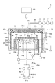
図1は、一つの例示的実施形態に係るプラズマ処理装置を概略的に示す図である。図1に示すプラズマ処理装置1は、容量結合型プラズマ処理装置である。プラズマ処理装置1は、チャンバ10を備えている。チャンバ10は、その中に内部空間10sを提供している。
FIG. 1 is a diagram schematically showing a plasma processing apparatus according to one exemplary embodiment. The
チャンバ10は、チャンバ本体12を含んでいる。チャンバ本体12は、略円筒形状を有している。内部空間10sは、チャンバ本体12の内側に提供されている。チャンバ本体12は、例えばアルミニウムから形成されている。チャンバ本体12の内壁面上には、耐腐食性を有する膜が設けられている。耐腐食性を有する膜は、酸化アルミニウム、酸化イットリウムといったセラミックから形成された膜であり得る。
The
チャンバ本体12の側壁には、通路12pが形成されている。基板Wは、内部空間10sとチャンバ10の外部との間で搬送されるときに、通路12pを通過する。通路12pは、ゲートバルブ12gにより開閉可能となっている。ゲートバルブ12gは、チャンバ本体12の側壁に沿って設けられている。
A
チャンバ本体12の底部上には、支持部13が設けられている。支持部13は、絶縁材料から形成されている。支持部13は、略円筒形状を有している。支持部13は、内部空間10sの中で、チャンバ本体12の底部から上方に延在している。支持部13は、基板支持器14を支持している。基板支持器14は、内部空間10sの中で基板Wを支持するように構成されている。
A
基板支持器14は、下部電極18及び静電チャック20を有している。基板支持器14は、電極プレート16を更に有し得る。電極プレート16、下部電極18、及び静電チャック20は、チャンバ10内に設けられている。電極プレート16は、例えばアルミニウムといった導体から形成されており、略円盤形状を有している。下部電極18は、電極プレート16上に設けられている。下部電極18は、例えばアルミニウムといった導体から形成されており、略円盤形状を有している。下部電極18は、電極プレート16に電気的に接続されている。
The
静電チャック20は、下部電極18上に設けられている。静電チャック20の上面の上には、基板Wが載置される。静電チャック20は、本体及び電極を有する。静電チャック20の本体は、略円盤形状を有し、誘電体から形成されている。静電チャック20の電極は、膜状の電極であり、静電チャック20の本体内に設けられている。静電チャック20の電極は、スイッチ20sを介して直流電源20pに接続されている。静電チャック20の電極に直流電源20pからの電圧が印加されると、静電チャック20と基板Wとの間で静電引力が発生する。発生した静電引力により、基板Wは、静電チャック20に引き付けられ、静電チャック20によって保持される。
The
基板支持器14の周縁部上には、フォーカスリングFRが搭載される。フォーカスリングFRは、基板Wに対するプラズマ処理の面内均一性を向上させるために設けられている。フォーカスリングFRは、略板状且つ環状をなしている。フォーカスリングFRは、限定されるものではないが、シリコン、炭化シリコン、又は石英から形成され得る。基板Wは、静電チャック20上、且つ、フォーカスリングFRによって囲まれた領域内に配置される。
A focus ring FR is mounted on the peripheral edge of the
下部電極18の内部には、流路18fが設けられている。流路18fには、チャンバ10の外部に設けられているチラーユニット22から配管22aを介して熱交換媒体(例えば冷媒)が供給される。流路18fに供給された熱交換媒体は、配管22bを介してチラーユニット22に戻される。プラズマ処理装置1では、静電チャック20上に載置された基板Wの温度が、熱交換媒体と下部電極18との熱交換により、調整される。
A
プラズマ処理装置1には、ガス供給ライン24が設けられている。ガス供給ライン24は、伝熱ガス供給機構からの伝熱ガス(例えばHeガス)を、静電チャック20の上面と基板Wの裏面との間の間隙に供給する。
The
プラズマ処理装置1は、上部電極30を更に備えている。上部電極30は、基板支持器14の上方に設けられている。上部電極30は、部材32を介して、チャンバ本体12の上部に支持されている。部材32は、絶縁性を有する材料から形成されている。上部電極30と部材32は、チャンバ本体12の上部開口を閉じている。
The
上部電極30は、天板34及び支持体36を含み得る。天板34の下面は、内部空間10sの側の下面であり、内部空間10sを画成している。天板34は、ジュール熱の少ない低抵抗の導電体又は半導体から形成され得る。天板34には、複数のガス吐出孔34aが形成されている。複数のガス吐出孔34aは、天板34をその板厚方向に貫通している。
The
支持体36は、天板34を着脱自在に支持する。支持体36は、アルミニウムといった導電性材料から形成される。支持体36の内部には、ガス拡散室36aが設けられている。支持体36には、複数のガス孔36bが形成されている。複数のガス孔36bは、ガス拡散室36aから下方に延びている。複数のガス孔36bは、複数のガス吐出孔34aにそれぞれ連通している。支持体36には、ガス導入口36cが形成されている。ガス導入口36cは、ガス拡散室36aに接続している。ガス導入口36cには、ガス供給管38が接続されている。
The
ガス供給管38には、バルブ群41、流量制御器群42、及びバルブ群43を介して、ガスソース群40が接続されている。ガスソース群40は、複数のガスソースを含んでいる。バルブ群41及びバルブ群43の各々は、複数の開閉バルブを含んでいる。流量制御器群42は、複数の流量制御器を含んでいる。流量制御器群42の複数の流量制御器の各々は、マスフローコントローラ又は圧力制御式の流量制御器である。ガスソース群40の複数のガスソースの各々は、バルブ群41の対応の開閉バルブ、流量制御器群42の対応の流量制御器、及びバルブ群43の対応の開閉バルブを介して、ガス供給管38に接続されている。
A
プラズマ処理装置1では、チャンバ本体12の内壁面に沿って、シールド46が着脱自在に設けられている。シールド46は、支持部13の外周にも設けられている。シールド46は、チャンバ本体12にエッチング副生物が付着することを防止する。シールド46は、例えば、アルミニウムから形成された部材の表面に耐腐食性を有する膜を形成することにより構成される。耐腐食性を有する膜は、酸化イットリウムといったセラミックから形成された膜であり得る。
In the
支持部13とチャンバ本体12の側壁との間には、バッフルプレート48が設けられている。バッフルプレート48は、例えば、アルミニウムから形成された部材の表面に耐腐食性を有する膜を形成することにより構成される。耐腐食性を有する膜は、酸化イットリウムといったセラミックから形成された膜であり得る。バッフルプレート48には、複数の貫通孔が形成されている。バッフルプレート48の下方、且つ、チャンバ本体12の底部には、排気口12eが設けられている。排気口12eには、排気管52を介して排気装置50が接続されている。排気装置50は、圧力調整弁及びターボ分子ポンプといった真空ポンプを有している。
A
プラズマ処理装置1は、高周波電源61を更に備えている。高周波電源61は、高周波電力HFを発生するように構成されている。高周波電力HFの基本周波数は、例えば13MHz〜200MHzの範囲内の周波数である。高周波電源61は、チャンバ10内のガスからプラズマを生成するために高周波電力HFを供給する。高周波電源61は、整合器62を介して下部電極18に電気的に接続されている。整合器62は、整合回路を有している。整合器62の整合回路は、高周波電源61の負荷側(下部電極側)のインピーダンスを、高周波電源61の出力インピーダンスに整合させるよう構成されている。整合器62と下部電極18との間にはフィルタ63が設けられていてもよい。フィルタ63は、高周波電力HFを通過させ、高周波電源61に向かう他の信号を低減させるか遮断するように構成されている。なお、別の実施形態では、高周波電源61は、整合器62を介して上部電極30に電気的に接続されていてもよい。
The
プラズマ処理装置1は、バイアス電源81を更に備えている。バイアス電源81は、下部電極18に電気的に接続されている。バイアス電源81は、基板支持器14にイオンを引き込むためにバイアス電力BPを発生するように構成されている。バイアス電力BPは、下部電極18に供給される。バイアス電源81と下部電極18との間にはフィルタ83が設けられていてもよい。フィルタ83は、バイアス電力BPを通過させ、バイアス電源81に向かう他の信号を低減させるか遮断するように構成されている。
The
以下、図1と共に、図2及び図3を参照する。図2は、一つの例示的実施形態に係るプラズマ処理装置の高周波電源及びバイアス電源の構成を示す図である。図3は、高周波電力(HF)、イオン密度(Ni)、電子温度(Te)、及びバイアス電力(パルス状の負極性の直流電圧BV)の例示的タイミングチャートである。 Hereinafter, FIG. 2 and FIG. 3 will be referred to together with FIG. FIG. 2 is a diagram showing a configuration of a high frequency power supply and a bias power supply of the plasma processing apparatus according to one exemplary embodiment. FIG. 3 is an exemplary timing chart of high frequency power (HF), ion density (Ni), electron temperature (Te), and bias power (pulse-like negative DC voltage BV).
一実施形態において、バイアス電源81は、バイアス電力BPとして、パルス状の負極性の直流電圧BVを周期CPで周期的に発生するように構成されている。直流電圧BVは、下部電極18に印加される。パルス状の負極性の直流電圧BVの繰り返し周波数、即ち、周期CPの逆数は、例えば1kHz〜800kHzの範囲内の周波数である。
In one embodiment, the
一実施形態において、バイアス電源81は、直流電源81a及びスイッチング素子81bを有していてもよい。直流電源81aは、負極性の直流電圧を発生する直流電源である。直流電源81aは、可変直流電源であってもよい。スイッチング素子81bは、直流電源81aと下部電極18との間で接続されている。スイッチング素子81bが導通状態になると、直流電源81aが下部電極18に導通して、負極性の直流電圧が下部電極18に印加される。一方、スイッチング素子81bが非導通状態になると、直流電源81aが下部電極18から電気的に切断されて、下部電極18に対する負極性の直流電圧の印加が停止される。かかるスイッチング素子81bの状態遷移により、パルス状の負極性の直流電圧BVが生成される。スイッチング素子81bの導通状態及び非導通状態は、後述する制御部80又は別のコントローラによって制御される。
In one embodiment, the
高周波電源61は、第1の期間P1において高周波電力HFを一つ以上のパルスPLとして供給するように構成されている。プラズマ処理装置1の場合には、第1の期間P1は、パルス状の負極性の直流電圧BVが下部電極18に印加されていない期間である。図3に示す例では、単一の第1の期間P1において、高周波電力HFの一つのパルスPLが供給される。
The high
高周波電源61は、第2の期間P2において高周波電力HFの供給を停止するように構成されている。プラズマ処理装置1の場合には、第2の期間P2は、パルス状の負極性の直流電圧BVが下部電極18に印加されている期間である。
The high
高周波電源61は、各パルスPLがその開始時点からそのピークが出現する時点まで徐々に増加するパワーレベルを有するように高周波電力HFを生成する。高周波電力HFの各パルスPLの立ち上がり時間は、高周波電源61から出力可能な高周波電力のパルスの最小の立ち上がり時間よりも長い時間に設定され得る。
The high
チャンバ10内のプラズマ中のイオンは、第2の期間P2では、基板Wに向けて加速される。その結果、第2の期間P2では、基板Wのエッチングが生じる。したがって、第2の期間P2では、基板Wから反応生成物が放出される。プラズマの電子温度が高い場合には、プラズマ中で反応生成物の再解離が生じる。反応生成物の再解離により生じた物質は基板W上に堆積し得る。プラズマ処理装置1では、高周波電力HFは第2の期間P2において供給されないので、第2の期間P2においてプラズマの電子温度は低い。したがって、プラズマ処理装置1によれば、反応生成物の再解離が抑制される。反応生成物の再解離が抑制されると、基板W上での堆積物の形成が抑制される。その結果、プラズマエッチングによって基板Wに形成された開口の縮小又は閉塞が抑制される。
The ions in the plasma in the
また、第1の期間P1においては、高周波電力HFが一つ以上のパルスPLとして供給される。各パルスPLのパワーレベルは、そのピークまで徐々に上昇する。したがって、電子温度のオーバーシュートが抑制される。その結果、プラズマ処理装置1によれば、ガスの過剰な解離が抑制される。故に、プラズマ処理装置1によれば、基板Wを比較的高いエッチングレートでエッチングすることが可能となる。
Further, in the first period P1, the high frequency power HF is supplied as one or more pulse PLs. The power level of each pulse PL gradually rises to its peak. Therefore, overshoot of electron temperature is suppressed. As a result, according to the
一実施形態において、高周波電源61は、図2に示すように、電力発生器61g及び出力部61aを有していてもよい。電力発生器61gは、高周波電力HFを発生するように構成されている。出力部61aは、電力発生器61gによって発生された高周波電力HFを出力するように構成されている。出力部61aは、整合器62を介して下部電極18に電気的に接続されている。
In one embodiment, the high
図4の(a)は複数の電力成分の合成電力の波形の一例を示す図であり、図4の(b)は図4の(a)に示す合成電力のパワースペクトルを示す図であり、図4の(c)は一例の高周波電力HFの波形を示す図である。図4の(c)に示すように、高周波電力HFは、周期的に供給されるパルス状の高周波電力である。即ち、高周波電力HFは、周期的に出現するパルスPLを含む。 FIG. 4A is a diagram showing an example of a waveform of the combined power of a plurality of power components, and FIG. 4B is a diagram showing a power spectrum of the combined power shown in FIG. 4A. FIG. 4C is a diagram showing a waveform of an example high-frequency power HF. As shown in FIG. 4C, the high-frequency power HF is a pulse-shaped high-frequency power that is periodically supplied. That is, the high frequency power HF includes a pulse PL that appears periodically.
一実施形態において、高周波電力HFは、複数の電力成分を含む。複数の電力成分は、複数の周波数をそれぞれ有する。図4の(b)に示すように、複数の周波数は、基本周波数f0に対して対称に設定されている。基本周波数f0は、例えば13MHz〜200MHzの範囲内の周波数である。一例では、基本周波数f0は、40.68MHzである。また、図4の(b)に示すように、複数の周波数は、所定の周波数fPの間隔で設定されている。一実施形態において、周波数fPは、周期CPの逆数である。図4の(b)に示す例では、複数の電力成分のそれぞれの周波数は、f0−(3/2)×fP、f0−fP/2、f0+fP/2、f0+(3/2)×fPである。 In one embodiment, the high frequency power HF comprises a plurality of power components. Each of the plurality of power components has a plurality of frequencies. As shown in FIG. 4 (b), a plurality of frequencies, are set symmetrically with respect to the fundamental frequency f 0. The fundamental frequency f 0 is, for example, a frequency in the range of 13 MHz to 200 MHz. In one example, the fundamental frequency f 0 is 40.68 MHz. Further, as shown in FIG. 4 (b), a plurality of frequency is set at intervals of a predetermined frequency f P. In one embodiment, the frequency f P is the reciprocal of the period CP. In the example shown in FIG. 4B, the frequencies of the plurality of power components are f 0 − (3/2) × f P , f 0 −f P / 2, f 0 + f P / 2, f 0. + (3/2) × f P.
複数の電力成分の合成電力の包絡線は、図4の(a)に示すように、複数のピーク群を含む。複数のピーク群の各々は、周期的に出現する複数のピークを含む。複数のピーク群の各々に含まれる複数のピークは、時間間隔TPで周期的に出現する。時間間隔TPは、周波数fPの逆数である。 As shown in FIG. 4A, the envelope of the combined power of the plurality of power components includes a plurality of peak groups. Each of the plurality of peak groups contains a plurality of peaks that appear periodically. A plurality of peaks included in each of the plurality of peaks are periodically appearing with time intervals T P. The time interval T P is the reciprocal of the frequency f P.
図4の(c)に示すように、高周波電力HFの包絡線は、時間間隔TPで出現するピークを有する。一実施形態では、高周波電力HFは、複数のピーク群のうち最大のパワーレベルを有するピークPMを含むピーク群から構成される。図4の(c)に示すように、高周波電力HFは、そのパワーレベルが、期間PAでゼロであるように設定されている。期間PAは、期間PPを除く期間である。期間PPは、高周波電力HFの包絡線のピークがそれぞれ出現する期間である。一実施形態では、期間PPは、ピークPMがそれぞれ出現する期間である。期間PPの各々は、高周波電力HFの包絡線の対応のピークの出現時点の直前の包絡線のゼロクロス領域ZAと当該出現時点の直後の包絡線のゼロクロス領域ZBとの間の期間である。ゼロクロス領域ZA及びゼロクロス領域ZBは、高周波電力HFの包絡線の振幅が実質的にゼロとみなせる値を有する時点であり得る。例えば、ゼロクロス領域ZA及びゼロクロス領域ZBの各々は、高周波電力HFの包絡線のピークのパワーレベルに対して30%以下又は10%以下のパワーレベルを、当該包絡線のパワーレベルが有する時点であってもよい。 As shown in FIG. 4 (c), the envelope of the high frequency power HF has a peak that appears at the time interval T P. In one embodiment, the high frequency power HF consists peak group comprising peaks P M having a maximum power level among the plurality of peaks. As shown in FIG. 4 (c), the high-frequency power HF, the power level is set to be zero in the period P A. Period P A is a period except for the period P P. Period P P is a period in which the peak of the envelope of the high frequency power HF appear respectively. In one embodiment, the period P P is a period in which the peak P M appears, respectively. Each of the periods P P is the period between the zero-crossing region Z A of the envelope immediately before the time of occurrence of the corresponding peak of the envelope of the high-frequency power HF and the zero-crossing region Z B of the envelope immediately after the time of occurrence. is there. The zero-cross region Z A and the zero-cross region Z B can be the time points at which the amplitude of the envelope of the high-frequency power HF has a value that can be regarded as substantially zero. For example, each of the zero-cross region Z A and the zero-cross region Z B has a power level of 30% or less or 10% or less with respect to the peak power level of the envelope of the high-frequency power HF at the time when the power level of the envelope has. It may be.
図4の(c)に示すように、高周波電力HFの各パルスは、そのピークまで徐々に増加するパワーレベルを有する。また、各パルスは、そのピークから徐々に減少するパワーレベルを有する。各パルスの直前のゼロクロス領域ZAと直後のゼロクロス領域ZBとの間の期間PPを除く期間PA、即ち各パルスの持続期間を除く期間では、高周波電力HFのパワーレベルはゼロに設定される。かかる高周波電力HFの帯域幅は、狭い。したがって、一実施形態の高周波電源61によれば、パルス状の高周波電力HFの帯域幅を狭くすることが可能となる。故に、プラズマ処理装置1によれば、高周波電力HFに対する反射波を抑制することが可能となる。
As shown in FIG. 4 (c), each pulse of high frequency power HF has a power level that gradually increases to its peak. Also, each pulse has a power level that gradually decreases from its peak. In the period other than the period P A, i.e. the duration of each pulse except the period P P between the zero-crossing area Z B immediately before and after the zero-crossing region Z A of each pulse, the power level of the high frequency power HF is set to zero Will be done. The bandwidth of such high frequency power HF is narrow. Therefore, according to the high
一実施形態においては、図2に示すように、電力発生器61gは、変調信号発生部64を有し得る。一実施形態において、電力発生器61gは、増幅器65を更に有していてもよい。変調信号発生部64は、変調高周波信号を生成する。高周波電力HFは、変調信号発生部64によって生成される変調高周波信号であってもよい。この場合には、増幅器65は不要である。或いは、高周波電力HFは、変調高周波信号が増幅器65によって増幅されることにより、生成されてもよい。
In one embodiment, as shown in FIG. 2, the
一実施形態においては、変調信号発生部64は、波形データ生成部71、量子化部72、逆フーリエ変換部73、及び変調部74を有している。一実施形態において、変調信号発生部64は、D/A変換部75,76、及びローパスフィルタ77,78を更に有していてもよい。変調信号発生部64は、例えばFPGA(Field−Programmable Gate Array)から構成され得る。或いは、変調信号発生部64は、幾つかの回路から形成されていてもよい。
In one embodiment, the modulation
波形データ生成部71は、変調高周波信号に対応する波形データを生成する。波形データ生成部71は、入力装置から波形データを生成するためのパラメータ(例えば、周波数及び位相等)を取得し、取得したパラメータを用いて波形データを生成するように構成されている。波形データ生成部71は、生成した波形データを量子化部72へ出力する。
The waveform
量子化部72は、波形データ生成部71によって生成された波形データを量子化して、量子化データを生成するように構成されている。逆フーリエ変換部73は、量子化データに逆フーリエ変換を適用して、Iデータ(同相成分)及びQデータ(直交位相成分)を生成するように構成されている。Iデータ及びQデータはそれぞれ、D/A変換部75,76、ローパスフィルタ77,78を経由して、変調部74に入力される。
The
変調部74は、それらの位相が互いに90°異なる二つの基準高周波信号を、入力されたIデータ及びQデータを用いてそれぞれ変調して、変調高周波信号を生成するように構成されている。
The
一実施形態において、変調部74は、PLL発振器74a(Phase Locked Loop 発振器)、移相器74b、ミキサ74c,74d、及び合成器74eを有する。
In one embodiment, the
PLL発振器74aは、基準高周波信号を生成するように構成されている。基準高周波信号は、ミキサ74cに入力される。また、基準高周波信号は、移相器74bに入力される。移相器74bは、ミキサ74cに入力される基準高周波信号に対して90°異なる位相を有する基準高周波信号を生成するように構成されている。具体的に、移相器74bは、入力された基準高周波信号の位相を90°シフトさせるように構成されている。移相器74bによって生成された基準高周波信号は、ミキサ74dに入力される。
The
ミキサ74cは、入力された基準高周波信号とIデータとの乗算を行うように構成されている。ミキサ74cの乗算により生成された信号は、合成器74eに入力される。ミキサ74dは、入力された基準高周波信号とQデータとの乗算を行うように構成されている。ミキサ74dの乗算により生成された信号は、合成器74eに入力される。合成器74eは、ミキサ74cとミキサ74dのそれぞれから入力された信号の加算を行って、変調高周波信号を生成するように構成されている。
The
一実施形態において、プラズマ処理装置1は、制御部80を更に備え得る。制御部80は、プロセッサ、メモリといった記憶部、入力装置、表示装置、信号の入出力インターフェイス等を備えるコンピュータであり得る。制御部80は、プラズマ処理装置1の各部を制御する。制御部80では、入力装置を用いて、オペレータがプラズマ処理装置1を管理するためにコマンドの入力操作等を行うことができる。また、制御部80では、表示装置により、プラズマ処理装置1の稼働状況を可視化して表示することができる。さらに、制御部80の記憶部には、制御プログラム及びレシピデータが格納されている。制御プログラムは、プラズマ処理装置1で各種処理を実行するために、制御部80のプロセッサによって実行される。制御部80のプロセッサが、制御プログラムを実行し、レシピデータに従ってプラズマ処理装置1の各部を制御することにより、プラズマ処理装置1においてプラズマ処理が実行される。
In one embodiment, the
一実施形態においては、制御部80又は別のコントローラが、直流電圧BVの周期CPの位相を設定するために、バイアス電源81の位相を制御してもよい。この実施形態によれば、パルスPLの供給の終了時点とパルス状の負極性の直流電圧BVの下部電極18への印加の開始時点との間の時間差T1(図3参照)を調整することが可能となる。したがって、パルス状の負極性の直流電圧BVの下部電極18への印加の開始までに、プラズマの電子温度を調整することが可能である。
In one embodiment, the
より具体的には、制御部80又は別のコントローラは、負極性の直流電圧BVの位相、即ち負極性の直流電圧BVの供給開始のタイミングを設定するよう、バイアス電源81を制御する。一実施形態では、制御部80又は別のコントローラは、スイッチング素子81bが非導通状態から導通状態に切り替わるタイミングを制御する。これにより、時間差T1が制御される。
More specifically, the
一実施形態において、制御部80又は別のコントローラは、パルス状の負極性の直流電圧BVの持続時間長PW(図3)を設定するようにバイアス電源81を更に制御してもよい。一実施形態では、制御部80又は別のコントローラは、スイッチング素子81bが導通状態を維持する時間長を制御することにより、持続時間長PWを設定する。これにより、パルス状の負極性の直流電圧BVの下部電極18への印加の終了時点とパルスPLの供給の開始時点との間の時間差T2(図3)を調整することが可能となる。
In one embodiment, the
以下、図5の(a)、図5の(b)、及び図5の(c)を参照する。別の例においては、図5の(b)に示すように、高周波電力HFの複数の電力成分の周波数は、f0−2×fP、f0−fP、f0、f0+fP、f0+2×fPである。この例では、図5の(a)に示すように、複数の電力成分の合成電力の包絡線は、四つのピーク群を含む。この例では、図5の(c)に示すように、高周波電力HFは、四つのピーク群のうち、最大のピークを含むピーク群から構成されている。なお、高周波電力HFは、二つ以上の電力成分から構成されていてもよい。二つ以上の電力成分それぞれの周波数は、基本周波数f0に対して対称に設定されており、且つ、所定の周波数fPで規定される間隔で設定される。 Hereinafter, reference is made to FIG. 5A, FIG. 5B, and FIG. 5C. In another example, as shown in FIG. 5 (b), the frequencies of the plurality of power components of the high-frequency power HF are f 0 -2 × f P , f 0 − f P , f 0 , f 0 + f P. , F 0 + 2 × f P. In this example, as shown in FIG. 5A, the envelope of the combined power of the plurality of power components includes four peak groups. In this example, as shown in FIG. 5C, the high-frequency power HF is composed of a peak group including the largest peak among the four peak groups. The high frequency power HF may be composed of two or more power components. The frequencies of each of the two or more power components are set symmetrically with respect to the fundamental frequency f 0 , and are set at intervals defined by a predetermined frequency f P.
以下、図6、図7、及び図8を参照して、別の実施形態に係るプラズマ処理装置について説明する。図6は、別の例示的実施形態に係るプラズマ処理装置を概略的に示す図である。図7は、別の例示的実施形態に係るプラズマ処理装置の高周波電源及びバイアス電源の構成を示す図である。図8は、高周波電力(HF)、イオン密度(Ni)、電子温度(Te)、及びバイアス電力(高周波バイアス電力LF)の別の例示的タイミングチャートである。 Hereinafter, the plasma processing apparatus according to another embodiment will be described with reference to FIGS. 6, 7, and 8. FIG. 6 is a diagram schematically showing a plasma processing apparatus according to another exemplary embodiment. FIG. 7 is a diagram showing a configuration of a high frequency power supply and a bias power supply of the plasma processing apparatus according to another exemplary embodiment. FIG. 8 is another exemplary timing chart of high frequency power (HF), ion density (Ni), electron temperature (Te), and bias power (high frequency bias power LF).
別の実施形態に係るプラズマ処理装置1Bは、バイアス電源81及びフィルタ83ではなく、バイアス電源81B及びフィルタ83Bを備えている。プラズマ処理装置1Bは、整合器82Bを更に備えている。他の点では、プラズマ処理装置1Bは、プラズマ処理装置1と同様に構成されている。
The
バイアス電源81Bは、基板支持器14にイオンを引き込むためのバイアス電力BPとして、高周波バイアス電力LFを発生するように構成されている。高周波バイアス電力LFの周波数は、周期CPの逆数である。高周波バイアス電力LFの周波数は、基本周波数f0よりも低い。高周波バイアス電力LFの周波数は、例えば400kHz〜13.56MHzの範囲内の周波数である。一例では、高周波バイアス電力LFの周波数は、400kHzである。一実施形態において、高周波バイアス電力LFの周波数は、上述の周波数fPであり得る。高周波バイアス電力LFは、下部電極18に供給される。
The
バイアス電源81Bは、整合器82Bを介して下部電極18に電気的に接続されている。整合器82Bは、整合回路を有している。整合器82Bの整合回路は、バイアス電源81Bの負荷側(下部電極側)のインピーダンスを、バイアス電源81Bの出力インピーダンスに整合させるよう構成されている。整合器82Bと下部電極18との間にはフィルタ83Bが設けられていてもよい。フィルタ83Bは、高周波バイアス電力LFを通過させ、バイアス電源81Bに向かう他の信号を低減させるか遮断するように構成されている。
The
図7に示すように、一実施形態において、バイアス電源81Bは、信号発生器81Ba及び増幅器81Bbを有していてもよい。信号発生器81Baは、高周波バイアス電力LFの周波数と同じ周波数を有する高周波信号を発生するように構成されている。信号発生器81Baによって生成された高周波信号は、増幅器81Bbに入力される。増幅器81Bbは、入力された高周波信号を増幅して、高周波バイアス電力LFを生成するように構成されている。
As shown in FIG. 7, in one embodiment, the
プラズマ処理装置1Bにおいて、高周波電源61は、図8に示すように、バイアス電源81Bから出力される高周波バイアス電力LFが正の電圧を有する第1の期間P1において高周波電力HFを一つ以上のパルスPLとして供給するように構成されている。図8に示す例では、単一の第1の期間P1において、高周波電力HFの一つのパルスPLが供給される。
In the
プラズマ処理装置1Bにおいて、高周波電源61は、バイアス電源81Bから出力される高周波バイアス電力LFが負の電圧を有する第2の期間P2において高周波電力HFの供給を停止するように構成されている。
In the
プラズマ処理装置1Bにおいてもプラズマ処理装置1と同様に、高周波電源61は、各パルスPLがその開始時点からそのピークが出現する時点まで徐々に増加するパワーレベルを有するように高周波電力HFを生成する。プラズマ処理装置1Bにおいてもプラズマ処理装置1と同様に、高周波電力HFの各パルスPLの立ち上がり時間は、高周波電源61から出力可能な高周波電力のパルスの最小の立ち上がり時間よりも長い時間に設定され得る。
In the
チャンバ10内のプラズマ中のイオンは、第2の期間P2では、基板Wに向けて加速される。その結果、第2の期間P2では、基板Wのエッチングが生じる。したがって、第2の期間P2では、基板Wから反応生成物が放出される。プラズマの電子温度が高い場合には、反応生成物の再解離が生じる。反応生成物の再解離により生じた物質は基板W上に堆積し得る。プラズマ処理装置1Bでは、高周波電力HFは第2の期間P2において供給されないので、第2の期間P2においてプラズマの電子温度は低い。したがって、プラズマ処理装置1Bによれば、反応生成物の再解離が抑制される。反応生成物の再解離が抑制されると、基板W上での堆積物の形成が抑制される。その結果、プラズマエッチングによって基板Wに形成された開口の縮小又は閉塞が抑制される。
The ions in the plasma in the
また、第1の期間P1においては、高周波電力HFが一つ以上のパルスPLとして供給される。各パルスPLのパワーレベルは、そのピークまで徐々に上昇する。したがって、電子温度のオーバーシュートが抑制される。その結果、プラズマ処理装置1Bによれば、ガスの過剰な解離が抑制される。故に、プラズマ処理装置1Bによれば、基板Wを比較的高いエッチングレートでエッチングすることが可能となる。
Further, in the first period P1, the high frequency power HF is supplied as one or more pulse PLs. The power level of each pulse PL gradually rises to its peak. Therefore, overshoot of electron temperature is suppressed. As a result, according to the
一実施形態において、制御部80又は別のコントローラが、高周波バイアス電力LFの位相を設定するためにバイアス電源81Bを制御してもよい。具体的には、制御部80又は別のコントローラから与えられるクロック信号により、高周波電源61とバイアス電源81Bは互いに同期されている。制御部80又は別のコントローラは、高周波電力HFと高周波バイアス電力LFとの間の位相差を設定するために、バイアス電源81Bに対して高周波バイアス電力LFの位相を設定する信号を与える。バイアス電源81Bは、与えられた位相で高周波バイアス電力LFを出力する。この実施形態によれば、パルスPLの供給の終了時点と下部電極18の電位が負のピークを有する時点との間の時間差TAを調整することが可能となる。また、下部電極18の電位が負のピークを有する時点とパルスPLの供給の開始時点との間の時間差TBを調整することが可能となる。
In one embodiment, the
以下、図9を参照する。図9は、高周波電力(HF)、イオン密度(Ni)、電子温度(Te)、及びバイアス電力(パルス状の負極性の直流電圧BV)の更に別の例示的タイミングチャートである。図9に示すように、更に別の実施形態においても、高周波電源61は、各パルスPLがその開始時点からそのピークが出現する時点まで徐々に増加するパワーレベルを有するように高周波電力HFを生成する。更に別の実施形態においては、高周波電力HFの各パルスPLの立ち上がり時間は、高周波電源61から出力可能な高周波電力のパルスの最小の立ち上がり時間よりも長い時間に設定され得る。この実施形態において、高周波電源61は、高周波電力の矩形パルスの立ち上がり時間、即ちランプ上昇時間を調整するランプアップ回路又はランプアップ機能を有していてもよい。なお、図9に示すように、更に別の実施形態においては、高周波電源61によって生成される各パルスPLの立ち下がり時間は、各パルスPLの立ち上がり時間よりも短くてもよい。例えば、各パルスは、ONからOFFに実質的に瞬時に又は連続的に切り替わってもよい。また、図9に示す実施形態においては、パルス状の負極性の直流電圧BVの代わりに、バイアス電力として高周波バイアス電力LFが用いられてもよい。
Hereinafter, FIG. 9 will be referred to. FIG. 9 is yet another exemplary timing chart of high frequency power (HF), ion density (Ni), electron temperature (Te), and bias power (pulse-like negative DC voltage BV). As shown in FIG. 9, in still another embodiment, the high
以下、図10を参照する。図10は、高周波電力(HF)及びバイアス電力(パルス状の負極性の直流電圧BV)の更に別の例示的タイミングチャートである。更に別の実施形態では、図10に示すように、高周波電源61は、第1の期間P1内において、プラズマの生成のために、複数のパルスPLを発生してもよい。第1の期間P1内において、複数のパルスPLは、連続的に又は断続的に、且つ、順に供給される。この実施形態によれば、第1の期間P1内におけるプラズマの電子温度の平均値が低減される。したがって、チャンバ10内でのガスの過剰な解離が更に抑制される。なお、図10に示す実施形態においては、パルス状の負極性の直流電圧BVの代わりに、バイアス電力として高周波バイアス電力LFが用いられてもよい。
Hereinafter, FIG. 10 will be referred to. FIG. 10 is yet another exemplary timing chart of high frequency power (HF) and bias power (pulse-like negative DC voltage BV). In yet another embodiment, as shown in FIG. 10, the high
以下、図11を参照する。図11は、別の例示的実施形態に係る高周波電源の構成を示す図である。図11に示すように、別の実施形態において、高周波電源61に代えて、高周波電源61Bが用いられてもよい。高周波電源61Bは、電力発生器61Bg及び出力部61aを有している。電力発生器61Bgは、高周波電力HFを発生するように構成されている。高周波電源61Bにおいて、出力部61aは、電力発生器61Bgによって生成された高周波電力HFを出力するように構成されている。
Hereinafter, FIG. 11 will be referred to. FIG. 11 is a diagram showing a configuration of a high frequency power supply according to another exemplary embodiment. As shown in FIG. 11, in another embodiment, the high
電力発生器61Bgは、変調信号発生部64Bを有している。電力発生器61Bgは、増幅器65を更に有していてもよい。変調信号発生部64Bは、変調高周波信号を生成する。高周波電力HFは、変調信号発生部64Bによって生成される変調高周波信号であってもよい。この場合には、増幅器65は不要である。或いは、高周波電力HFは、変調高周波信号が増幅器65によって増幅されることにより、生成されてもよい。
The power generator 61Bg has a modulation
変調信号発生部64Bは、複数の信号発生器911〜91N、加算器92、及びスイッチング回路93を有し得る。ここで、「N」は、2以上の整数である。複数の信号発生器911〜91Nは、複数の高周波信号をそれぞれ発生するように構成されている。複数の高周波信号それぞれの周波数は、基本周波数f0に対して対称に設定されている。複数の高周波信号それぞれの周波数は、所定の周波数fPの間隔で設定されている。
The modulated
加算器92は、複数の信号発生器911〜91Nからの複数の高周波信号を加算して合成信号を生成するように構成されている。合成信号の包絡線は、時間間隔TPで周期的に出現するピークを有する。スイッチング回路93は、変調高周波信号を合成信号から生成するように構成されている。変調高周波信号は、その振幅レベルが、合成信号の包絡線のピークの各々の出現時点の直前の当該包絡線のゼロクロス領域ZAと該出現時点の直後の当該包絡線のゼロクロス領域ZBとの間の期間PPを除く期間PAでゼロであるように設定される。かかる高周波電源61Bも、高周波電源61と同様に高周波電力HFを生成することが可能である。即ち、高周波電源61Bも、高周波電力のパルスを生成することができる。
The
以上、種々の例示的実施形態について説明してきたが、上述した例示的実施形態に限定されることなく、様々な追加、省略、置換、及び変更がなされてもよい。また、異なる実施形態における要素を組み合わせて他の実施形態を形成することが可能である。 Although various exemplary embodiments have been described above, various additions, omissions, substitutions, and changes may be made without being limited to the above-mentioned exemplary embodiments. It is also possible to combine elements in different embodiments to form other embodiments.
別の実施形態において、プラズマ処理装置は、誘導結合型のプラズマ処理装置といった他のタイプのプラズマ処理装置であってもよい。誘導結合型のプラズマ処理装置では、高周波電力HFは、誘導結合プラズマを生成するためのアンテナに供給される。 In another embodiment, the plasma processing apparatus may be another type of plasma processing apparatus such as an inductively coupled plasma processing apparatus. In an inductively coupled plasma processing apparatus, high frequency power HF is supplied to an antenna for generating inductively coupled plasma.
以上の説明から、本開示の種々の実施形態は、説明の目的で本明細書で説明されており、本開示の範囲及び主旨から逸脱することなく種々の変更をなし得ることが、理解されるであろう。したがって、本明細書に開示した種々の実施形態は限定することを意図しておらず、真の範囲と主旨は、添付の特許請求の範囲によって示される。 From the above description, it is understood that the various embodiments of the present disclosure are described herein for purposes of explanation and that various modifications can be made without departing from the scope and gist of the present disclosure. Will. Therefore, the various embodiments disclosed herein are not intended to be limiting, and the true scope and gist is indicated by the appended claims.
1…プラズマ処理装置、10…チャンバ、61…高周波電源、81…バイアス電源。 1 ... Plasma processing device, 10 ... Chamber, 61 ... High frequency power supply, 81 ... Bias power supply.
Claims (12)
下部電極を有し、前記チャンバ内で基板を支持するように構成された基板支持器と、
前記チャンバ内でガスからプラズマを生成するために高周波電力を発生するよう構成された高周波電源と、
前記下部電極に電気的に接続されており、前記基板支持器にイオンを引き込むためのバイアス電力を発生するように構成されたバイアス電源と、
を備え、
前記バイアス電源は、前記バイアス電力として、パルス状の負極性の直流電圧を周期的に発生するように構成されており、
前記高周波電源は、前記パルス状の負極性の直流電圧が前記下部電極に印加されていない第1の期間において前記高周波電力を一つ以上のパルスとして供給し、前記パルス状の負極性の直流電圧が前記下部電極に印加されている第2の期間において前記高周波電力の供給を停止するように構成されており、
前記高周波電源は、前記一つ以上のパルスの各々がその開始時点からそのピークが出現する時点まで徐々に増加するパワーレベルを有するように前記高周波電力を生成する、
プラズマ処理装置。 With the chamber
A substrate support having a lower electrode and configured to support the substrate in the chamber.
A high frequency power supply configured to generate high frequency power to generate plasma from the gas in the chamber.
A bias power supply that is electrically connected to the lower electrode and is configured to generate bias power to draw ions into the substrate support.
With
The bias power supply is configured to periodically generate a pulsed negative electrode DC voltage as the bias power.
The high frequency power supply supplies the high frequency power as one or more pulses in the first period in which the pulsed negative electrode DC voltage is not applied to the lower electrode, and the pulsed negative electrode DC voltage. Is configured to stop the supply of the high frequency power in the second period when is applied to the lower electrode.
The high frequency power source produces the high frequency power such that each of the one or more pulses has a power level that gradually increases from its start point to the point where its peak appears.
Plasma processing equipment.
下部電極を有し、前記チャンバ内で基板を支持するように構成された基板支持器と、
前記チャンバ内でガスからプラズマを生成するために高周波電力を発生するよう構成された高周波電源と、
前記下部電極に電気的に接続されており、前記基板支持器にイオンを引き込むためのバイアス電力を発生するように構成されたバイアス電源と、
を備え、
前記バイアス電源は、前記バイアス電力として、高周波バイアス電力を発生するように構成されており、
前記高周波電源は、前記バイアス電源から出力される前記高周波バイアス電力が正の電圧を有する第1の期間において前記高周波電力を一つ以上のパルスとして供給し、前記バイアス電源から出力される前記高周波バイアス電力が負の電圧を有する第2の期間において前記高周波電力の供給を停止するように構成されており、
前記高周波電源は、前記一つ以上のパルスの各々がその開始時点からそのピークが出現する時点まで徐々に増加するパワーレベルを有するように前記高周波電力を生成する、
プラズマ処理装置。 With the chamber
A substrate support having a lower electrode and configured to support the substrate in the chamber.
A high frequency power supply configured to generate high frequency power to generate plasma from the gas in the chamber.
A bias power supply that is electrically connected to the lower electrode and is configured to generate bias power to draw ions into the substrate support.
With
The bias power supply is configured to generate high-frequency bias power as the bias power.
The high frequency power supply supplies the high frequency power as one or more pulses in a first period in which the high frequency bias power output from the bias power supply has a positive voltage, and the high frequency bias output from the bias power supply. It is configured to stop the supply of the high frequency power in the second period when the power has a negative voltage.
The high frequency power source produces the high frequency power such that each of the one or more pulses has a power level that gradually increases from its start point to the point where its peak appears.
Plasma processing equipment.
前記高周波電力を発生するように構成された電力発生器と、
前記電力発生器によって発生された前記高周波電力を出力するように構成された出力部と、
を有する、請求項1〜6の何れか一項に記載のプラズマ処理装置。 The high frequency power supply
A power generator configured to generate the high frequency power and
An output unit configured to output the high-frequency power generated by the power generator, and an output unit.
The plasma processing apparatus according to any one of claims 1 to 6.
請求項7に記載のプラズマ処理装置。 The power generator is the high-frequency power including a plurality of power components each having a plurality of frequencies set symmetrically with respect to a fundamental frequency at predetermined frequency intervals, and the envelope thereof is the predetermined frequency or It has peaks that appear periodically at time intervals defined by a frequency that is a multiple of twice or more the predetermined frequency, and its power level is the zero cross region of the envelope immediately before each occurrence of the peak. It is configured to generate the high frequency power, which is set to be zero in the period excluding the period between the frequency and the zero cross region of the envelope immediately after the output.
The plasma processing apparatus according to claim 7.
波形データ生成部と、
前記波形データ生成部によって生成された波形データを量子化して、量子化データを生成するように構成された量子化部と、
前記量子化データに逆フーリエ変換を適用して、Iデータ及びQデータを生成するように構成された逆フーリエ変換部と、
それらの位相が互いに90°異なる二つの基準高周波信号を前記Iデータ及び前記Qデータを用いて変調して、変調高周波信号を生成するように構成された変調部と、
を有し、前記変調高周波信号から前記高周波電力を生成するように構成されている、
請求項7又は8に記載のプラズマ処理装置。 The power generator
Waveform data generator and
A quantization unit configured to generate quantization data by quantizationing the waveform data generated by the waveform data generation unit,
An inverse Fourier transform unit configured to generate I data and Q data by applying an inverse Fourier transform to the quantized data.
A modulation unit configured to generate a modulated high-frequency signal by modulating two reference high-frequency signals whose phases differ by 90 ° from each other using the I data and the Q data.
And is configured to generate the high frequency power from the modulated high frequency signal.
The plasma processing apparatus according to claim 7 or 8.
Priority Applications (7)
| Application Number | Priority Date | Filing Date | Title |
|---|---|---|---|
| CN202310809321.5A CN116844934A (en) | 2019-02-05 | 2020-01-21 | Plasma processing apparatus |
| CN202010070561.4A CN111524782B (en) | 2019-02-05 | 2020-01-21 | Plasma processing apparatus |
| KR1020200008821A KR102280293B1 (en) | 2019-02-05 | 2020-01-22 | Plasma processing apparatus |
| US16/752,376 US10707054B1 (en) | 2019-02-05 | 2020-01-24 | Plasma processing apparatus |
| US16/891,886 US11205561B2 (en) | 2019-02-05 | 2020-06-03 | Plasma processing apparatus |
| KR1020210093033A KR102580453B1 (en) | 2019-02-05 | 2021-07-15 | Plasma processing apparatus |
| US17/500,691 US11631572B2 (en) | 2019-02-05 | 2021-10-13 | Plasma processing apparatus |
Applications Claiming Priority (2)
| Application Number | Priority Date | Filing Date | Title |
|---|---|---|---|
| JP2019018833 | 2019-02-05 | ||
| JP2019018833 | 2019-02-05 |
Related Child Applications (1)
| Application Number | Title | Priority Date | Filing Date |
|---|---|---|---|
| JP2020191041A Division JP7060664B2 (en) | 2019-02-05 | 2020-11-17 | Plasma processing equipment |
Publications (2)
| Publication Number | Publication Date |
|---|---|
| JP2020126998A JP2020126998A (en) | 2020-08-20 |
| JP6797273B2 true JP6797273B2 (en) | 2020-12-09 |
Family
ID=72085033
Family Applications (3)
| Application Number | Title | Priority Date | Filing Date |
|---|---|---|---|
| JP2019236679A Active JP6797273B2 (en) | 2019-02-05 | 2019-12-26 | Plasma processing equipment |
| JP2020191041A Active JP7060664B2 (en) | 2019-02-05 | 2020-11-17 | Plasma processing equipment |
| JP2022066927A Active JP7395645B2 (en) | 2019-02-05 | 2022-04-14 | plasma processing equipment |
Family Applications After (2)
| Application Number | Title | Priority Date | Filing Date |
|---|---|---|---|
| JP2020191041A Active JP7060664B2 (en) | 2019-02-05 | 2020-11-17 | Plasma processing equipment |
| JP2022066927A Active JP7395645B2 (en) | 2019-02-05 | 2022-04-14 | plasma processing equipment |
Country Status (1)
| Country | Link |
|---|---|
| JP (3) | JP6797273B2 (en) |
Families Citing this family (3)
| Publication number | Priority date | Publication date | Assignee | Title |
|---|---|---|---|---|
| JP7122268B2 (en) * | 2019-02-05 | 2022-08-19 | 東京エレクトロン株式会社 | Plasma processing equipment |
| WO2022168642A1 (en) * | 2021-02-04 | 2022-08-11 | 東京エレクトロン株式会社 | Plasma processing device, and plasma processing method |
| JP2022137603A (en) * | 2021-03-09 | 2022-09-22 | 東京エレクトロン株式会社 | Plasma processing method and plasma processing apparatus |
Family Cites Families (9)
| Publication number | Priority date | Publication date | Assignee | Title |
|---|---|---|---|---|
| JP2000144434A (en) * | 1998-11-09 | 2000-05-26 | Sekisui Chem Co Ltd | Production of functionally gradient material |
| JP2001358129A (en) * | 2000-06-16 | 2001-12-26 | Matsushita Electric Ind Co Ltd | Method and apparatus for plasma processing |
| US9123509B2 (en) * | 2007-06-29 | 2015-09-01 | Varian Semiconductor Equipment Associates, Inc. | Techniques for plasma processing a substrate |
| JP5542509B2 (en) * | 2010-04-05 | 2014-07-09 | 株式会社東芝 | Plasma processing apparatus and plasma processing method |
| JP6312405B2 (en) * | 2013-11-05 | 2018-04-18 | 東京エレクトロン株式会社 | Plasma processing equipment |
| JP6309398B2 (en) * | 2014-08-29 | 2018-04-11 | 株式会社ダイヘン | High frequency power supply |
| JP6817889B2 (en) * | 2016-05-10 | 2021-01-20 | 東京エレクトロン株式会社 | Plasma processing equipment and plasma processing method |
| JP6770868B2 (en) * | 2016-10-26 | 2020-10-21 | 東京エレクトロン株式会社 | Method for impedance matching of plasma processing equipment |
| US10927449B2 (en) * | 2017-01-25 | 2021-02-23 | Applied Materials, Inc. | Extension of PVD chamber with multiple reaction gases, high bias power, and high power impulse source for deposition, implantation, and treatment |
-
2019
- 2019-12-26 JP JP2019236679A patent/JP6797273B2/en active Active
-
2020
- 2020-11-17 JP JP2020191041A patent/JP7060664B2/en active Active
-
2022
- 2022-04-14 JP JP2022066927A patent/JP7395645B2/en active Active
Also Published As
| Publication number | Publication date |
|---|---|
| JP7395645B2 (en) | 2023-12-11 |
| JP2020126998A (en) | 2020-08-20 |
| JP2022105037A (en) | 2022-07-12 |
| JP7060664B2 (en) | 2022-04-26 |
| JP2021036612A (en) | 2021-03-04 |
Similar Documents
| Publication | Publication Date | Title |
|---|---|---|
| KR102280293B1 (en) | Plasma processing apparatus | |
| JP7060664B2 (en) | Plasma processing equipment | |
| TW202305935A (en) | Control method and plasma treatment device | |
| JP7122268B2 (en) | Plasma processing equipment | |
| JP5822795B2 (en) | Plasma processing equipment | |
| JP7345382B2 (en) | Plasma processing equipment and control method | |
| TW201739160A (en) | Direct current pulsing plasma systems | |
| JP7374362B2 (en) | Plasma treatment method and plasma treatment device | |
| JP6817889B2 (en) | Plasma processing equipment and plasma processing method | |
| JP6180890B2 (en) | Plasma processing method | |
| JP6043852B2 (en) | Plasma processing equipment | |
| JP2020061546A (en) | Plasma processing apparatus and control method | |
| WO2023286715A1 (en) | Plasma processing method and plasma processing device |
Legal Events
| Date | Code | Title | Description |
|---|---|---|---|
| A621 | Written request for application examination |
Free format text: JAPANESE INTERMEDIATE CODE: A621 Effective date: 20200722 |
|
| A871 | Explanation of circumstances concerning accelerated examination |
Free format text: JAPANESE INTERMEDIATE CODE: A871 Effective date: 20200722 |
|
| A975 | Report on accelerated examination |
Free format text: JAPANESE INTERMEDIATE CODE: A971005 Effective date: 20201005 |
|
| TRDD | Decision of grant or rejection written | ||
| A01 | Written decision to grant a patent or to grant a registration (utility model) |
Free format text: JAPANESE INTERMEDIATE CODE: A01 Effective date: 20201020 |
|
| A61 | First payment of annual fees (during grant procedure) |
Free format text: JAPANESE INTERMEDIATE CODE: A61 Effective date: 20201117 |
|
| R150 | Certificate of patent or registration of utility model |
Ref document number: 6797273 Country of ref document: JP Free format text: JAPANESE INTERMEDIATE CODE: R150 |
|
| R250 | Receipt of annual fees |
Free format text: JAPANESE INTERMEDIATE CODE: R250 |