JP6795657B2 - Thin film transistor substrate and thin film transistor substrate manufacturing method - Google Patents
Thin film transistor substrate and thin film transistor substrate manufacturing method Download PDFInfo
- Publication number
- JP6795657B2 JP6795657B2 JP2019135113A JP2019135113A JP6795657B2 JP 6795657 B2 JP6795657 B2 JP 6795657B2 JP 2019135113 A JP2019135113 A JP 2019135113A JP 2019135113 A JP2019135113 A JP 2019135113A JP 6795657 B2 JP6795657 B2 JP 6795657B2
- Authority
- JP
- Japan
- Prior art keywords
- film
- insulating film
- layer side
- metal film
- lower layer
- Prior art date
- Legal status (The legal status is an assumption and is not a legal conclusion. Google has not performed a legal analysis and makes no representation as to the accuracy of the status listed.)
- Active
Links
- 239000000758 substrate Substances 0.000 title claims description 87
- 239000010409 thin film Substances 0.000 title claims description 49
- 238000004519 manufacturing process Methods 0.000 title description 29
- 239000010408 film Substances 0.000 claims description 622
- 229910052751 metal Inorganic materials 0.000 claims description 201
- 239000002184 metal Substances 0.000 claims description 201
- 239000004065 semiconductor Substances 0.000 claims description 151
- VYPSYNLAJGMNEJ-UHFFFAOYSA-N Silicium dioxide Chemical compound O=[Si]=O VYPSYNLAJGMNEJ-UHFFFAOYSA-N 0.000 claims description 9
- 229910052814 silicon oxide Inorganic materials 0.000 claims description 9
- 239000010410 layer Substances 0.000 description 132
- 238000005530 etching Methods 0.000 description 86
- 238000000034 method Methods 0.000 description 19
- 239000004973 liquid crystal related substance Substances 0.000 description 18
- 230000007547 defect Effects 0.000 description 10
- 229920002120 photoresistant polymer Polymers 0.000 description 9
- 230000009467 reduction Effects 0.000 description 9
- QVGXLLKOCUKJST-UHFFFAOYSA-N atomic oxygen Chemical compound [O] QVGXLLKOCUKJST-UHFFFAOYSA-N 0.000 description 7
- 239000000463 material Substances 0.000 description 7
- 239000001301 oxygen Substances 0.000 description 7
- 229910052760 oxygen Inorganic materials 0.000 description 7
- 230000008569 process Effects 0.000 description 6
- 239000011701 zinc Substances 0.000 description 6
- 229910007541 Zn O Inorganic materials 0.000 description 4
- 230000009471 action Effects 0.000 description 4
- 230000000694 effects Effects 0.000 description 4
- 230000005684 electric field Effects 0.000 description 4
- 229910004298 SiO 2 Inorganic materials 0.000 description 3
- XUIMIQQOPSSXEZ-UHFFFAOYSA-N Silicon Chemical compound [Si] XUIMIQQOPSSXEZ-UHFFFAOYSA-N 0.000 description 3
- 239000004020 conductor Substances 0.000 description 3
- 229910052733 gallium Inorganic materials 0.000 description 3
- 229910052738 indium Inorganic materials 0.000 description 3
- 239000011159 matrix material Substances 0.000 description 3
- 230000003071 parasitic effect Effects 0.000 description 3
- 229910021420 polycrystalline silicon Inorganic materials 0.000 description 3
- 229910052710 silicon Inorganic materials 0.000 description 3
- 239000010703 silicon Substances 0.000 description 3
- GYHNNYVSQQEPJS-UHFFFAOYSA-N Gallium Chemical compound [Ga] GYHNNYVSQQEPJS-UHFFFAOYSA-N 0.000 description 2
- XLOMVQKBTHCTTD-UHFFFAOYSA-N Zinc monoxide Chemical compound [Zn]=O XLOMVQKBTHCTTD-UHFFFAOYSA-N 0.000 description 2
- 229910021417 amorphous silicon Inorganic materials 0.000 description 2
- 230000015572 biosynthetic process Effects 0.000 description 2
- 239000011521 glass Substances 0.000 description 2
- APFVFJFRJDLVQX-UHFFFAOYSA-N indium atom Chemical compound [In] APFVFJFRJDLVQX-UHFFFAOYSA-N 0.000 description 2
- 239000011810 insulating material Substances 0.000 description 2
- 238000009413 insulation Methods 0.000 description 2
- 239000007769 metal material Substances 0.000 description 2
- 238000000059 patterning Methods 0.000 description 2
- 238000009832 plasma treatment Methods 0.000 description 2
- 238000009751 slip forming Methods 0.000 description 2
- 229910052725 zinc Inorganic materials 0.000 description 2
- 229910052581 Si3N4 Inorganic materials 0.000 description 1
- HCHKCACWOHOZIP-UHFFFAOYSA-N Zinc Chemical compound [Zn] HCHKCACWOHOZIP-UHFFFAOYSA-N 0.000 description 1
- 239000000956 alloy Substances 0.000 description 1
- 229910045601 alloy Inorganic materials 0.000 description 1
- 238000000137 annealing Methods 0.000 description 1
- 230000000903 blocking effect Effects 0.000 description 1
- 239000003086 colorant Substances 0.000 description 1
- 239000007772 electrode material Substances 0.000 description 1
- 238000001962 electrophoresis Methods 0.000 description 1
- 239000007789 gas Substances 0.000 description 1
- AMGQUBHHOARCQH-UHFFFAOYSA-N indium;oxotin Chemical compound [In].[Sn]=O AMGQUBHHOARCQH-UHFFFAOYSA-N 0.000 description 1
- 238000010030 laminating Methods 0.000 description 1
- 239000003094 microcapsule Substances 0.000 description 1
- 239000000203 mixture Substances 0.000 description 1
- 229920005591 polysilicon Polymers 0.000 description 1
- 230000008439 repair process Effects 0.000 description 1
- 239000011347 resin Substances 0.000 description 1
- 229920005989 resin Polymers 0.000 description 1
- HQVNEWCFYHHQES-UHFFFAOYSA-N silicon nitride Chemical compound N12[Si]34N5[Si]62N3[Si]51N64 HQVNEWCFYHHQES-UHFFFAOYSA-N 0.000 description 1
- 239000002356 single layer Substances 0.000 description 1
- 239000007787 solid Substances 0.000 description 1
- YVTHLONGBIQYBO-UHFFFAOYSA-N zinc indium(3+) oxygen(2-) Chemical compound [O--].[Zn++].[In+3] YVTHLONGBIQYBO-UHFFFAOYSA-N 0.000 description 1
- 239000011787 zinc oxide Substances 0.000 description 1
Images


Classifications
-
- H—ELECTRICITY
- H01—ELECTRIC ELEMENTS
- H01L—SEMICONDUCTOR DEVICES NOT COVERED BY CLASS H10
- H01L27/00—Devices consisting of a plurality of semiconductor or other solid-state components formed in or on a common substrate
- H01L27/02—Devices consisting of a plurality of semiconductor or other solid-state components formed in or on a common substrate including semiconductor components specially adapted for rectifying, oscillating, amplifying or switching and having at least one potential-jump barrier or surface barrier; including integrated passive circuit elements with at least one potential-jump barrier or surface barrier
- H01L27/12—Devices consisting of a plurality of semiconductor or other solid-state components formed in or on a common substrate including semiconductor components specially adapted for rectifying, oscillating, amplifying or switching and having at least one potential-jump barrier or surface barrier; including integrated passive circuit elements with at least one potential-jump barrier or surface barrier the substrate being other than a semiconductor body, e.g. an insulating body
- H01L27/1214—Devices consisting of a plurality of semiconductor or other solid-state components formed in or on a common substrate including semiconductor components specially adapted for rectifying, oscillating, amplifying or switching and having at least one potential-jump barrier or surface barrier; including integrated passive circuit elements with at least one potential-jump barrier or surface barrier the substrate being other than a semiconductor body, e.g. an insulating body comprising a plurality of TFTs formed on a non-semiconducting substrate, e.g. driving circuits for AMLCDs
- H01L27/1222—Devices consisting of a plurality of semiconductor or other solid-state components formed in or on a common substrate including semiconductor components specially adapted for rectifying, oscillating, amplifying or switching and having at least one potential-jump barrier or surface barrier; including integrated passive circuit elements with at least one potential-jump barrier or surface barrier the substrate being other than a semiconductor body, e.g. an insulating body comprising a plurality of TFTs formed on a non-semiconducting substrate, e.g. driving circuits for AMLCDs with a particular composition, shape or crystalline structure of the active layer
- H01L27/1225—Devices consisting of a plurality of semiconductor or other solid-state components formed in or on a common substrate including semiconductor components specially adapted for rectifying, oscillating, amplifying or switching and having at least one potential-jump barrier or surface barrier; including integrated passive circuit elements with at least one potential-jump barrier or surface barrier the substrate being other than a semiconductor body, e.g. an insulating body comprising a plurality of TFTs formed on a non-semiconducting substrate, e.g. driving circuits for AMLCDs with a particular composition, shape or crystalline structure of the active layer with semiconductor materials not belonging to the group IV of the periodic table, e.g. InGaZnO
-
- G—PHYSICS
- G02—OPTICS
- G02F—OPTICAL DEVICES OR ARRANGEMENTS FOR THE CONTROL OF LIGHT BY MODIFICATION OF THE OPTICAL PROPERTIES OF THE MEDIA OF THE ELEMENTS INVOLVED THEREIN; NON-LINEAR OPTICS; FREQUENCY-CHANGING OF LIGHT; OPTICAL LOGIC ELEMENTS; OPTICAL ANALOGUE/DIGITAL CONVERTERS
- G02F1/00—Devices or arrangements for the control of the intensity, colour, phase, polarisation or direction of light arriving from an independent light source, e.g. switching, gating or modulating; Non-linear optics
- G02F1/01—Devices or arrangements for the control of the intensity, colour, phase, polarisation or direction of light arriving from an independent light source, e.g. switching, gating or modulating; Non-linear optics for the control of the intensity, phase, polarisation or colour
- G02F1/13—Devices or arrangements for the control of the intensity, colour, phase, polarisation or direction of light arriving from an independent light source, e.g. switching, gating or modulating; Non-linear optics for the control of the intensity, phase, polarisation or colour based on liquid crystals, e.g. single liquid crystal display cells
- G02F1/133—Constructional arrangements; Operation of liquid crystal cells; Circuit arrangements
- G02F1/136—Liquid crystal cells structurally associated with a semi-conducting layer or substrate, e.g. cells forming part of an integrated circuit
- G02F1/1362—Active matrix addressed cells
- G02F1/136227—Through-hole connection of the pixel electrode to the active element through an insulation layer
-
- H—ELECTRICITY
- H01—ELECTRIC ELEMENTS
- H01L—SEMICONDUCTOR DEVICES NOT COVERED BY CLASS H10
- H01L27/00—Devices consisting of a plurality of semiconductor or other solid-state components formed in or on a common substrate
- H01L27/02—Devices consisting of a plurality of semiconductor or other solid-state components formed in or on a common substrate including semiconductor components specially adapted for rectifying, oscillating, amplifying or switching and having at least one potential-jump barrier or surface barrier; including integrated passive circuit elements with at least one potential-jump barrier or surface barrier
- H01L27/12—Devices consisting of a plurality of semiconductor or other solid-state components formed in or on a common substrate including semiconductor components specially adapted for rectifying, oscillating, amplifying or switching and having at least one potential-jump barrier or surface barrier; including integrated passive circuit elements with at least one potential-jump barrier or surface barrier the substrate being other than a semiconductor body, e.g. an insulating body
- H01L27/1214—Devices consisting of a plurality of semiconductor or other solid-state components formed in or on a common substrate including semiconductor components specially adapted for rectifying, oscillating, amplifying or switching and having at least one potential-jump barrier or surface barrier; including integrated passive circuit elements with at least one potential-jump barrier or surface barrier the substrate being other than a semiconductor body, e.g. an insulating body comprising a plurality of TFTs formed on a non-semiconducting substrate, e.g. driving circuits for AMLCDs
- H01L27/1218—Devices consisting of a plurality of semiconductor or other solid-state components formed in or on a common substrate including semiconductor components specially adapted for rectifying, oscillating, amplifying or switching and having at least one potential-jump barrier or surface barrier; including integrated passive circuit elements with at least one potential-jump barrier or surface barrier the substrate being other than a semiconductor body, e.g. an insulating body comprising a plurality of TFTs formed on a non-semiconducting substrate, e.g. driving circuits for AMLCDs with a particular composition or structure of the substrate
-
- H—ELECTRICITY
- H01—ELECTRIC ELEMENTS
- H01L—SEMICONDUCTOR DEVICES NOT COVERED BY CLASS H10
- H01L27/00—Devices consisting of a plurality of semiconductor or other solid-state components formed in or on a common substrate
- H01L27/02—Devices consisting of a plurality of semiconductor or other solid-state components formed in or on a common substrate including semiconductor components specially adapted for rectifying, oscillating, amplifying or switching and having at least one potential-jump barrier or surface barrier; including integrated passive circuit elements with at least one potential-jump barrier or surface barrier
- H01L27/12—Devices consisting of a plurality of semiconductor or other solid-state components formed in or on a common substrate including semiconductor components specially adapted for rectifying, oscillating, amplifying or switching and having at least one potential-jump barrier or surface barrier; including integrated passive circuit elements with at least one potential-jump barrier or surface barrier the substrate being other than a semiconductor body, e.g. an insulating body
- H01L27/1214—Devices consisting of a plurality of semiconductor or other solid-state components formed in or on a common substrate including semiconductor components specially adapted for rectifying, oscillating, amplifying or switching and having at least one potential-jump barrier or surface barrier; including integrated passive circuit elements with at least one potential-jump barrier or surface barrier the substrate being other than a semiconductor body, e.g. an insulating body comprising a plurality of TFTs formed on a non-semiconducting substrate, e.g. driving circuits for AMLCDs
- H01L27/124—Devices consisting of a plurality of semiconductor or other solid-state components formed in or on a common substrate including semiconductor components specially adapted for rectifying, oscillating, amplifying or switching and having at least one potential-jump barrier or surface barrier; including integrated passive circuit elements with at least one potential-jump barrier or surface barrier the substrate being other than a semiconductor body, e.g. an insulating body comprising a plurality of TFTs formed on a non-semiconducting substrate, e.g. driving circuits for AMLCDs with a particular composition, shape or layout of the wiring layers specially adapted to the circuit arrangement, e.g. scanning lines in LCD pixel circuits
- H01L27/1244—Devices consisting of a plurality of semiconductor or other solid-state components formed in or on a common substrate including semiconductor components specially adapted for rectifying, oscillating, amplifying or switching and having at least one potential-jump barrier or surface barrier; including integrated passive circuit elements with at least one potential-jump barrier or surface barrier the substrate being other than a semiconductor body, e.g. an insulating body comprising a plurality of TFTs formed on a non-semiconducting substrate, e.g. driving circuits for AMLCDs with a particular composition, shape or layout of the wiring layers specially adapted to the circuit arrangement, e.g. scanning lines in LCD pixel circuits for preventing breakage, peeling or short circuiting
-
- H—ELECTRICITY
- H01—ELECTRIC ELEMENTS
- H01L—SEMICONDUCTOR DEVICES NOT COVERED BY CLASS H10
- H01L27/00—Devices consisting of a plurality of semiconductor or other solid-state components formed in or on a common substrate
- H01L27/02—Devices consisting of a plurality of semiconductor or other solid-state components formed in or on a common substrate including semiconductor components specially adapted for rectifying, oscillating, amplifying or switching and having at least one potential-jump barrier or surface barrier; including integrated passive circuit elements with at least one potential-jump barrier or surface barrier
- H01L27/12—Devices consisting of a plurality of semiconductor or other solid-state components formed in or on a common substrate including semiconductor components specially adapted for rectifying, oscillating, amplifying or switching and having at least one potential-jump barrier or surface barrier; including integrated passive circuit elements with at least one potential-jump barrier or surface barrier the substrate being other than a semiconductor body, e.g. an insulating body
- H01L27/1214—Devices consisting of a plurality of semiconductor or other solid-state components formed in or on a common substrate including semiconductor components specially adapted for rectifying, oscillating, amplifying or switching and having at least one potential-jump barrier or surface barrier; including integrated passive circuit elements with at least one potential-jump barrier or surface barrier the substrate being other than a semiconductor body, e.g. an insulating body comprising a plurality of TFTs formed on a non-semiconducting substrate, e.g. driving circuits for AMLCDs
- H01L27/1248—Devices consisting of a plurality of semiconductor or other solid-state components formed in or on a common substrate including semiconductor components specially adapted for rectifying, oscillating, amplifying or switching and having at least one potential-jump barrier or surface barrier; including integrated passive circuit elements with at least one potential-jump barrier or surface barrier the substrate being other than a semiconductor body, e.g. an insulating body comprising a plurality of TFTs formed on a non-semiconducting substrate, e.g. driving circuits for AMLCDs with a particular composition or shape of the interlayer dielectric specially adapted to the circuit arrangement
-
- H—ELECTRICITY
- H01—ELECTRIC ELEMENTS
- H01L—SEMICONDUCTOR DEVICES NOT COVERED BY CLASS H10
- H01L27/00—Devices consisting of a plurality of semiconductor or other solid-state components formed in or on a common substrate
- H01L27/02—Devices consisting of a plurality of semiconductor or other solid-state components formed in or on a common substrate including semiconductor components specially adapted for rectifying, oscillating, amplifying or switching and having at least one potential-jump barrier or surface barrier; including integrated passive circuit elements with at least one potential-jump barrier or surface barrier
- H01L27/12—Devices consisting of a plurality of semiconductor or other solid-state components formed in or on a common substrate including semiconductor components specially adapted for rectifying, oscillating, amplifying or switching and having at least one potential-jump barrier or surface barrier; including integrated passive circuit elements with at least one potential-jump barrier or surface barrier the substrate being other than a semiconductor body, e.g. an insulating body
- H01L27/1214—Devices consisting of a plurality of semiconductor or other solid-state components formed in or on a common substrate including semiconductor components specially adapted for rectifying, oscillating, amplifying or switching and having at least one potential-jump barrier or surface barrier; including integrated passive circuit elements with at least one potential-jump barrier or surface barrier the substrate being other than a semiconductor body, e.g. an insulating body comprising a plurality of TFTs formed on a non-semiconducting substrate, e.g. driving circuits for AMLCDs
- H01L27/1259—Multistep manufacturing methods
- H01L27/1262—Multistep manufacturing methods with a particular formation, treatment or coating of the substrate
-
- H—ELECTRICITY
- H01—ELECTRIC ELEMENTS
- H01L—SEMICONDUCTOR DEVICES NOT COVERED BY CLASS H10
- H01L27/00—Devices consisting of a plurality of semiconductor or other solid-state components formed in or on a common substrate
- H01L27/02—Devices consisting of a plurality of semiconductor or other solid-state components formed in or on a common substrate including semiconductor components specially adapted for rectifying, oscillating, amplifying or switching and having at least one potential-jump barrier or surface barrier; including integrated passive circuit elements with at least one potential-jump barrier or surface barrier
- H01L27/12—Devices consisting of a plurality of semiconductor or other solid-state components formed in or on a common substrate including semiconductor components specially adapted for rectifying, oscillating, amplifying or switching and having at least one potential-jump barrier or surface barrier; including integrated passive circuit elements with at least one potential-jump barrier or surface barrier the substrate being other than a semiconductor body, e.g. an insulating body
- H01L27/1214—Devices consisting of a plurality of semiconductor or other solid-state components formed in or on a common substrate including semiconductor components specially adapted for rectifying, oscillating, amplifying or switching and having at least one potential-jump barrier or surface barrier; including integrated passive circuit elements with at least one potential-jump barrier or surface barrier the substrate being other than a semiconductor body, e.g. an insulating body comprising a plurality of TFTs formed on a non-semiconducting substrate, e.g. driving circuits for AMLCDs
- H01L27/1259—Multistep manufacturing methods
- H01L27/127—Multistep manufacturing methods with a particular formation, treatment or patterning of the active layer specially adapted to the circuit arrangement
-
- H—ELECTRICITY
- H01—ELECTRIC ELEMENTS
- H01L—SEMICONDUCTOR DEVICES NOT COVERED BY CLASS H10
- H01L29/00—Semiconductor devices adapted for rectifying, amplifying, oscillating or switching, or capacitors or resistors with at least one potential-jump barrier or surface barrier, e.g. PN junction depletion layer or carrier concentration layer; Details of semiconductor bodies or of electrodes thereof ; Multistep manufacturing processes therefor
- H01L29/66—Types of semiconductor device ; Multistep manufacturing processes therefor
- H01L29/66007—Multistep manufacturing processes
- H01L29/66969—Multistep manufacturing processes of devices having semiconductor bodies not comprising group 14 or group 13/15 materials
-
- H—ELECTRICITY
- H01—ELECTRIC ELEMENTS
- H01L—SEMICONDUCTOR DEVICES NOT COVERED BY CLASS H10
- H01L29/00—Semiconductor devices adapted for rectifying, amplifying, oscillating or switching, or capacitors or resistors with at least one potential-jump barrier or surface barrier, e.g. PN junction depletion layer or carrier concentration layer; Details of semiconductor bodies or of electrodes thereof ; Multistep manufacturing processes therefor
- H01L29/66—Types of semiconductor device ; Multistep manufacturing processes therefor
- H01L29/68—Types of semiconductor device ; Multistep manufacturing processes therefor controllable by only the electric current supplied, or only the electric potential applied, to an electrode which does not carry the current to be rectified, amplified or switched
- H01L29/76—Unipolar devices, e.g. field effect transistors
- H01L29/772—Field effect transistors
- H01L29/78—Field effect transistors with field effect produced by an insulated gate
- H01L29/786—Thin film transistors, i.e. transistors with a channel being at least partly a thin film
- H01L29/78606—Thin film transistors, i.e. transistors with a channel being at least partly a thin film with supplementary region or layer in the thin film or in the insulated bulk substrate supporting it for controlling or increasing the safety of the device
- H01L29/78633—Thin film transistors, i.e. transistors with a channel being at least partly a thin film with supplementary region or layer in the thin film or in the insulated bulk substrate supporting it for controlling or increasing the safety of the device with a light shield
-
- H—ELECTRICITY
- H01—ELECTRIC ELEMENTS
- H01L—SEMICONDUCTOR DEVICES NOT COVERED BY CLASS H10
- H01L29/00—Semiconductor devices adapted for rectifying, amplifying, oscillating or switching, or capacitors or resistors with at least one potential-jump barrier or surface barrier, e.g. PN junction depletion layer or carrier concentration layer; Details of semiconductor bodies or of electrodes thereof ; Multistep manufacturing processes therefor
- H01L29/66—Types of semiconductor device ; Multistep manufacturing processes therefor
- H01L29/68—Types of semiconductor device ; Multistep manufacturing processes therefor controllable by only the electric current supplied, or only the electric potential applied, to an electrode which does not carry the current to be rectified, amplified or switched
- H01L29/76—Unipolar devices, e.g. field effect transistors
- H01L29/772—Field effect transistors
- H01L29/78—Field effect transistors with field effect produced by an insulated gate
- H01L29/786—Thin film transistors, i.e. transistors with a channel being at least partly a thin film
- H01L29/7869—Thin film transistors, i.e. transistors with a channel being at least partly a thin film having a semiconductor body comprising an oxide semiconductor material, e.g. zinc oxide, copper aluminium oxide, cadmium stannate
Description
本発明は、薄膜トランジスタ基板及び薄膜トランジスタ基板の製造方法に関する。 The present invention relates to a thin film transistor substrate and a method for manufacturing a thin film transistor substrate.
従来、液晶表示装置に備えられる薄膜トランジスタ基板の一例として下記特許文献1に記載されたものが知られている。この特許文献1に記載された薄膜トランジスタ基板は、基板上の画素領域に、透明酸化物層、絶縁膜、導電層が順次積層され、前記導電層はゲート信号線に接続される薄膜トランジスタのゲート電極を有し、前記透明酸化物層は少なくとも前記ゲート電極の直下のチャネル領域部を除いた他の領域が導電体化され、この導電体化された部分でソース信号線、このソース信号線に接続される前記薄膜トランジスタのソース領域部、画素電極、この画素電極に接続される前記薄膜トランジスタのドレイン領域部を構成している。 Conventionally, as an example of a thin film transistor substrate provided in a liquid crystal display device, the one described in Patent Document 1 below is known. In the thin film transistor substrate described in Patent Document 1, a transparent oxide layer, an insulating film, and a conductive layer are sequentially laminated on a pixel region on the substrate, and the conductive layer is a gate electrode of a thin film transistor connected to a gate signal line. The transparent oxide layer has, at least, a region other than the channel region immediately below the gate electrode is made into a conductor, and the conductive portion is connected to the source signal line and the source signal line. It constitutes a source region portion of the thin film transistor, a pixel electrode, and a drain region portion of the thin film transistor connected to the pixel electrode.
上記した特許文献1に記載された薄膜トランジスタ基板には、透明酸化物層上に直接成膜された金属膜をエッチングすることでソース信号線を形成する構成が記載されている。しかしながら、この構成では、透明酸化物層上の金属膜をエッチングする際に膜残りが生じると、金属膜の残された部分によって例えば画素電極とソース信号線とが短絡するなどの不良が生じるおそれがある。また、透明酸化物層上の金属膜をエッチングする際に透明酸化物層がオーバーエッチングされるおそれもある。 The thin film transistor substrate described in Patent Document 1 described above describes a configuration in which a source signal line is formed by etching a metal film directly formed on a transparent oxide layer. However, in this configuration, if a film residue is generated when the metal film on the transparent oxide layer is etched, defects such as a short circuit between the pixel electrode and the source signal line may occur due to the remaining portion of the metal film. There is. In addition, the transparent oxide layer may be overetched when the metal film on the transparent oxide layer is etched.
本発明は上記のような事情に基づいて完成されたものであって、第2金属膜のエッチングに伴う不具合の発生を抑制することを目的とする。 The present invention has been completed based on the above circumstances, and an object of the present invention is to suppress the occurrence of defects due to etching of the second metal film.
(1)本発明に係る薄膜トランジスタ基板の一実施形態は、半導体膜と、前記半導体膜の上層側に配される第1絶縁膜と、前記第1絶縁膜の上層側に配される第1金属膜と、前記第1金属膜の上層側に配される第2絶縁膜と、前記第2絶縁膜の上層側に配される第2金属膜と、前記第2金属膜からなるソース配線と、薄膜トランジスタを構成していて前記第1金属膜からなるゲート電極と、前記薄膜トランジスタを構成していて前記半導体膜の一部からなり前記ゲート電極と重畳するよう配されるチャネル領域と、前記薄膜トランジスタを構成していて前記半導体膜の一部を低抵抗化してなり前記チャネル領域に連なるとともに少なくとも前記第2絶縁膜に開口形成されたコンタクトホールを通して前記ソース配線に接続されるソース領域と、前記薄膜トランジスタを構成していて前記半導体膜の一部を低抵抗化してなり前記チャネル領域に対して前記ソース領域側とは反対側から連なるドレイン領域と、前記半導体膜の一部を低抵抗化してなり前記ドレイン領域に連なる画素電極と、を備える。 (1) One embodiment of the thin film transistor substrate according to the present invention includes a semiconductor film, a first insulating film arranged on the upper layer side of the semiconductor film, and a first metal arranged on the upper layer side of the first insulating film. A film, a second insulating film arranged on the upper layer side of the first metal film, a second metal film arranged on the upper layer side of the second insulating film, and a source wiring composed of the second metal film. The thin film transistor is composed of a gate electrode that constitutes the thin film transistor and is composed of the first metal film, a channel region that constitutes the thin film transistor and is composed of a part of the semiconductor film and is arranged so as to overlap the gate electrode. A part of the semiconductor film is reduced in resistance to be connected to the channel region, and at least a source region connected to the source wiring through a contact hole formed as an opening in the second insulating film and the thin film transistor are configured. The resistance of a part of the semiconductor film is reduced so that the drain region is continuous from the side opposite to the source region side with respect to the channel region, and a part of the semiconductor film is reduced in resistance to the drain region. It is provided with a pixel electrode connected to the above.
(2)また、本発明に係る薄膜トランジスタ基板のある実施形態は、上記(1)の構成に加え、前記半導体膜の下層側に配される下層側絶縁膜と、前記下層側絶縁膜の下層側に配される下層側金属膜と、前記下層側金属膜からなり少なくとも前記チャネル領域と重畳するよう配される遮光部と、を備える。 (2) Further, in an embodiment of the thin film transistor substrate according to the present invention, in addition to the configuration of (1) above, a lower layer side insulating film arranged on the lower layer side of the semiconductor film and a lower layer side of the lower layer side insulating film are provided. It is provided with a lower layer side metal film arranged in the lower layer side and a light-shielding portion composed of the lower layer side metal film and arranged so as to overlap with at least the channel region.
(3)また、本発明に係る薄膜トランジスタ基板のある実施形態は、上記(2)の構成に加え、前記遮光部は、下層側ゲート電極とされる。 (3) Further, in an embodiment of the thin film transistor substrate according to the present invention, in addition to the configuration of (2) above, the light-shielding portion is a lower layer side gate electrode.
(4)また、本発明に係る薄膜トランジスタ基板のある実施形態は、上記(3)の構成に加え、前記第2金属膜からなり前記第2絶縁膜に開口形成された第1電極間コンタクトホールと少なくとも前記下層側絶縁膜及び前記第2絶縁膜に開口形成された第2電極間コンタクトホールとを通して前記ゲート電極と前記下層側ゲート電極とにそれぞれ接続される電極間接続部と、前記下層側金属膜からなり前記下層側ゲート電極に連なるゲート配線と、を備える。 (4) Further, in an embodiment of the thin film transistor substrate according to the present invention, in addition to the configuration of (3) above, a contact hole between the first electrodes made of the second metal film and having an opening formed in the second insulating film is provided. An electrode-to-electrode connection portion connected to the gate electrode and the lower-layer side gate electrode through at least the lower-layer side insulating film and a second electrode-to-electrode contact hole formed in the second insulating film, and the lower-layer side metal. It is provided with a gate wiring made of a film and connected to the lower layer side gate electrode.
(5)また、本発明に係る薄膜トランジスタ基板のある実施形態は、上記(1)、上記(2)または、上記(3)の構成に加え、前記第1金属膜からなり前記ゲート電極に連なるゲート配線を備える。 (5) Further, in an embodiment of the thin film transistor substrate according to the present invention, in addition to the above (1), the above (2), or the above (3), a gate made of the first metal film and connected to the gate electrode. Provide wiring.
(6)また、本発明に係る薄膜トランジスタ基板のある実施形態は、上記(1)、上記(2)、上記(3)、上記(4)または、上記(5)の構成に加え、前記半導体膜の一部を低抵抗化してなり前記ソース領域に連なるとともに少なくとも一部が前記ソース配線と重畳するよう配される補助ソース配線を備える。 (6) Further, in an embodiment of the thin film transistor substrate according to the present invention, in addition to the above (1), the above (2), the above (3), the above (4), or the above (5), the semiconductor film. Auxiliary source wiring is provided so that a part of the wiring is reduced in resistance and connected to the source region, and at least a part thereof is arranged so as to overlap the source wiring.
(7)また、本発明に係る薄膜トランジスタ基板のある実施形態は、上記(6)の構成に加え、前記ソース配線は、前記補助ソース配線よりも幅狭とされる。 (7) Further, in an embodiment of the thin film transistor substrate according to the present invention, in addition to the configuration of (6) above, the source wiring is narrower than the auxiliary source wiring.
(8)また、本発明に係る薄膜トランジスタ基板のある実施形態は、上記(1)、上記(2)、上記(3)、上記(4)、上記(5)、上記(6)または、上記(7)の構成に加え、前記第2絶縁膜は、少なくとも前記ドレイン領域及び前記画素電極を覆うよう配される。 (8) Further, certain embodiments of the thin film transistor substrate according to the present invention include the above (1), the above (2), the above (3), the above (4), the above (5), the above (6), or the above ( In addition to the configuration of 7), the second insulating film is arranged so as to cover at least the drain region and the pixel electrode.
(9)また、本発明に係る薄膜トランジスタ基板のある実施形態は、上記(1)、上記(2)、上記(3)、上記(4)、上記(5)、上記(6)または、上記(7)の構成に加え、前記第2絶縁膜は、少なくともシリコン酸化物を含んでいて少なくとも前記ソース領域及び前記ドレイン領域のうちの前記チャネル領域に隣接する部分とはそれぞれ重畳するものの、前記ドレイン領域のうちの前記画素電極に隣接する部分と前記画素電極とは非重畳となるよう形成される。 (9) Further, certain embodiments of the thin film transistor substrate according to the present invention include the above (1), the above (2), the above (3), the above (4), the above (5), the above (6), or the above ( In addition to the configuration of 7), the second insulating film contains at least silicon oxide and overlaps with at least the portion of the source region and the drain region adjacent to the channel region, but the drain region. The portion of the pixel electrode adjacent to the pixel electrode and the pixel electrode are formed so as not to overlap with each other.
(10)また、本発明に係る薄膜トランジスタ基板のある実施形態は、上記(1)、上記(2)、上記(3)、上記(4)、上記(5)、上記(6)、上記(7)、上記(8)または、上記(9)の構成に加え、前記第1絶縁膜は、前記第1金属膜と重畳する範囲に選択的に配される。 (10) Further, certain embodiments of the thin film transistor substrate according to the present invention include the above (1), the above (2), the above (3), the above (4), the above (5), the above (6), and the above (7). ), The above (8) or the above (9), the first insulating film is selectively arranged in a range where it overlaps with the first metal film.
(11)また、本発明に係る薄膜トランジスタ基板のある実施形態は、上記(1)、上記(2)、上記(3)、上記(4)、上記(5)、上記(6)、上記(7)、上記(8)、上記(9)または、上記(10)の構成に加え、前記半導体膜は、酸化物半導体からなる。 (11) Further, certain embodiments of the thin film transistor substrate according to the present invention include the above (1), the above (2), the above (3), the above (4), the above (5), the above (6), and the above (7). ), The above (8), the above (9), or the above (10), the semiconductor film is made of an oxide semiconductor.
(12)本発明に係る薄膜トランジスタ基板の製造方法の一実施形態は、半導体膜を成膜する半導体膜成膜工程と、前記半導体膜の上層側に第1絶縁膜を成膜する第1絶縁膜成膜工程と、前記第1絶縁膜の上層側に第1金属膜を成膜する第1金属膜成膜工程と、前記第1金属膜を前記第1絶縁膜と共にエッチングすることで薄膜トランジスタを構成していて前記第1金属膜からなるゲート電極を形成する第1金属膜エッチング工程と、前記半導体膜をエッチングする半導体膜エッチング工程と、前記半導体膜のうち、前記ゲート電極と重畳するチャネル領域以外の部分を低抵抗化することで、前記薄膜トランジスタを構成していて前記チャネル領域に連なるソース領域と、前記薄膜トランジスタを構成していて前記チャネル領域に対して前記ソース領域側とは反対側から連なるドレイン領域と、前記ドレイン領域に連なる画素電極と、を形成する低抵抗化工程と、前記第1金属膜の上層側に第2絶縁膜を成膜する第2絶縁膜成膜工程と、前記第2絶縁膜をエッチングすることで前記ソース領域の一部と重畳する部分にコンタクトホールを開口形成する第2絶縁膜エッチング工程と、前記第2絶縁膜の上層側に第2金属膜を成膜する第2金属膜成膜工程と、前記第2金属膜をエッチングすることで前記コンタクトホールを通して前記ソース領域に接続されるソース配線を形成する第2金属膜エッチング工程と、を備える。 (12) One embodiment of the method for manufacturing a thin film substrate according to the present invention includes a semiconductor film forming step of forming a semiconductor film and a first insulating film forming a first insulating film on the upper layer side of the semiconductor film. A semiconductor film is formed by a film forming step, a first metal film forming step of forming a first metal film on the upper layer side of the first insulating film, and etching the first metal film together with the first insulating film. The first metal film etching step of forming the gate electrode made of the first metal film, the semiconductor film etching step of etching the semiconductor film, and the semiconductor film other than the channel region overlapping with the gate electrode. By lowering the resistance of the portion, the source region that constitutes the thin film and is connected to the channel region and the drain that constitutes the thin film and is connected to the channel region from the side opposite to the source region side. A low resistance step of forming a region and a pixel electrode connected to the drain region, a second insulating film forming step of forming a second insulating film on the upper layer side of the first metal film, and the second insulating film forming step. A second insulating film etching step of forming a contact hole in a portion overlapping a part of the source region by etching the insulating film, and a second metal film forming a second metal film on the upper layer side of the second insulating film. The two metal film forming step includes a second metal film etching step of forming a source wiring connected to the source region through the contact hole by etching the second metal film.
このように、半導体膜成膜工程、第1絶縁膜成膜工程及び第1金属膜成膜工程を経て半導体膜、第1絶縁膜及び第1金属膜が成膜される。第1金属膜エッチング工程では、第1金属膜が第1絶縁膜と共にエッチングされ、半導体膜エッチング工程では、半導体膜がエッチングされる。そして、低抵抗化工程では、半導体膜のうちのチャネル領域を除いた部分が低抵抗化されることで、ソース領域、ドレイン領域及び画素電極が形成される。このようにすれば、仮に画素電極が透明電極膜からなる場合に比べると、透明電極膜の成膜やエッチングが不要になるとともに透明電極膜を他の導電膜と絶縁するための絶縁膜を追加せずに済むので、製造コストの低下などを図る上で好適となる。第2絶縁膜成膜工程を経て成膜された第2絶縁膜は、第2絶縁膜エッチング工程にてエッチングされることで、ソース領域の一部と重畳する部分にコンタクトホールが開口形成される。第2金属膜成膜工程を経て第2絶縁膜の上層側に成膜された第2金属膜は、第2金属膜エッチング工程にてエッチングされることで、コンタクトホールを通してソース領域に接続されるソース配線が形成される。この第2金属膜エッチング工程では、半導体膜は少なくとも一部が第2絶縁膜により覆われた状態とされている。従って、仮に第2金属膜のエッチングが不十分で膜残りが生じたとしても、その膜残り部分によって例えばソース配線と半導体膜のうちの低抵抗化されてなる部分とが短絡するといった不良が生じるのを避けることができる。しかも、半導体膜の少なくとも一部が第2絶縁膜により覆われることで、第2金属膜エッチング工程にて半導体膜がオーバーエッチングされる事態が避けられる。 In this way, the semiconductor film, the first insulating film, and the first metal film are formed through the semiconductor film forming step, the first insulating film forming step, and the first metal film forming step. In the first metal film etching step, the first metal film is etched together with the first insulating film, and in the semiconductor film etching step, the semiconductor film is etched. Then, in the resistance reduction step, the portion of the semiconductor film excluding the channel region is reduced in resistance to form a source region, a drain region, and a pixel electrode. In this way, compared to the case where the pixel electrode is made of a transparent electrode film, the film formation and etching of the transparent electrode film become unnecessary, and an insulating film for insulating the transparent electrode film from other conductive films is added. Since it is not necessary to do so, it is suitable for reducing the manufacturing cost. The second insulating film formed through the second insulating film film forming step is etched in the second insulating film etching step to form a contact hole in a portion overlapping with a part of the source region. .. The second metal film formed on the upper layer side of the second insulating film through the second metal film film forming step is etched in the second metal film etching step to be connected to the source region through the contact hole. The source wiring is formed. In this second metal film etching step, at least a part of the semiconductor film is covered with the second insulating film. Therefore, even if the etching of the second metal film is insufficient and a film residue is generated, a defect such as a short circuit between the source wiring and the low resistance portion of the semiconductor film occurs due to the film remaining portion. Can be avoided. Moreover, since at least a part of the semiconductor film is covered with the second insulating film, it is possible to avoid a situation in which the semiconductor film is overetched in the second metal film etching step.
(13)また、本発明に係る薄膜トランジスタ基板の製造方法のある実施形態は、上記(12)に加え、前記第1金属膜エッチング工程は、前記半導体膜エッチング工程の前に行われる。 (13) Further, in an embodiment of the method for manufacturing a thin film transistor substrate according to the present invention, in addition to the above (12), the first metal film etching step is performed before the semiconductor film etching step.
本発明によれば、第2金属膜のエッチングに伴う不具合の発生を抑制することができる。 According to the present invention, it is possible to suppress the occurrence of defects due to etching of the second metal film.
<実施形態1>
本発明の実施形態1を図1から図8によって説明する。本実施形態では、液晶パネル(表示パネル)を構成するアレイ基板(薄膜トランジスタ基板)10について例示する。なお、各図面の一部にはX軸、Y軸及びZ軸を示しており、各軸方向が各図面で示した方向となるように描かれている。また、図2から図8の上側を表側とし、下側を裏側とする。
<Embodiment 1>
Embodiment 1 of the present invention will be described with reference to FIGS. 1 to 8. In this embodiment, the array substrate (thin film transistor substrate) 10 constituting the liquid crystal panel (display panel) will be illustrated. The X-axis, Y-axis, and Z-axis are shown in a part of each drawing, and each axis direction is drawn so as to be the direction shown in each drawing. Further, the upper side of FIGS. 2 to 8 is the front side, and the lower side is the back side.
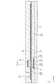
液晶パネルは、アレイ基板10と図示しないCF基板(対向基板)とが、間に図示しない液晶層を挟んだ状態で貼り合わせられた構成とされ、アレイ基板10及びCF基板の外面側にはそれぞれ図示しない偏光板が貼り付けられている。液晶パネルは、その表示面が画像を表示可能な表示領域と、表示領域を取り囲む非表示領域と、に区分されている。図1は、アレイ基板10における表示領域の平面図である。アレイ基板10における表示領域には、図1に示すように、スイッチング素子であるTFT(薄膜トランジスタ)11及び画素電極12が多数個マトリクス状(行列状)に並んで設けられる。TFT11及び画素電極12の周りには、格子状をなすゲート配線(走査線)13及びソース配線(データ線、信号線)14が取り囲むようにして配設されている。ゲート配線13とソース配線14とがそれぞれTFT11のゲート電極11Aとソース領域11Bとに接続され、画素電極12がTFT11のドレイン領域11Cに接続されている。そして、TFT11は、ゲート配線13及びソース配線14にそれぞれ供給される各種信号に基づいて駆動され、その駆動に伴って画素電極12への電位の供給が制御される。画素電極12は、ゲート配線13及びソース配線14により囲まれた縦長の方形の領域に配されている。画素電極12には、自身の長辺方向(Y軸方向)に沿って延在する複数(図1では3本)のスリット12Aが形成されている。アレイ基板10の表示領域には、画素電極12と重畳する形で概ねベタ状の共通電極15が形成されている。互いに重畳する画素電極12と共通電極15との間に電位差が生じると、アレイ基板10の板面に沿う成分に加えて、アレイ基板10の板面に対する法線方向の成分を含むフリンジ電界(斜め電界)が液晶層のうちのスリット12A付近の部分に印加される。つまり、本実施形態に係るアレイ基板10を備える液晶パネルは、動作モードがFFS(Fringe Field Switching)モードとされる。なお、本実施形態では、各図面においてゲート配線13の延在方向がX軸方向と、ソース配線14の延在方向がY軸方向と、それぞれ一致する。
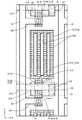
The liquid crystal panel has a configuration in which an
より詳しくは、TFT11は、図1に示すように、接続対象とされる画素電極12に対してY軸方向について図1に示す下側に隣り合う配置とされる。TFT11は、ゲート配線13の一部からなるゲート電極11Aを有する。TFT11は、ソース配線14から分岐してなるソース分岐部14Aに接続されるソース領域11Bを有する。ソース分岐部14Aは、ソース配線14のうち、ゲート配線13と交差する部分に対してY軸方向について接続対象となる画素電極12側とは反対側に配されている。ソース分岐部14Aは、X軸方向に沿って延在しており、その先端部がソース領域11Bに接続されている。ソース領域11Bには、ソース配線14に伝送される画像信号がソース分岐部14Aを介して供給される。ソース領域11Bは、Y軸方向に沿って延在している。TFT11は、ソース領域11Bに対してY軸方向について間隔を空けて配されるドレイン領域11Cを有する。ドレイン領域11Cは、Y軸方向に沿って延在していてソース領域11B(チャネル領域11D)側とは反対側の端部が画素電極12に連ねられている。TFT11は、ゲート電極11Aと重畳するとともに、ソース領域11B及びドレイン領域11Cに連なるチャネル領域11Dを有する。チャネル領域11Dは、Y軸方向に沿って延在し、その一端側がソース領域11Bに、他端側がドレイン領域11Cに、それぞれ連ねられている。そして、ゲート電極11Aに供給される走査信号に基づいてTFT11が駆動されると、ソース配線14に供給される画像信号(電荷)は、ソース分岐部14A及びソース領域11Bからチャネル領域11Dを介してドレイン領域11Cへと供給される。その結果、画素電極12が画像信号に基づいた電位に充電される。また、アレイ基板10の表示領域には、少なくとも上記したチャネル領域11Dと重畳する位置に遮光部16が設けられている。遮光部16は、チャネル領域11Dに対して下層側から照射される光を遮ることが可能とされる。このような光は、例えば液晶パネルに対してバックライト装置から照射される表示のための光とされる。チャネル領域11Dへ向かう上記した光が遮光部16によって遮られることで、チャネル領域11Dに光が照射された場合に生じ得るTFT11の特性の変動を抑制することができる。
More specifically, as shown in FIG. 1, the
一方、CF基板の表示領域には、アレイ基板10側の各画素電極12と対向状をなす位置に多数個のカラーフィルタ(図示せず)がマトリクス状に並んで設けられている。カラーフィルタは、R(赤色),G(緑色),B(青色)の三色が所定の順で繰り返し並んで配されてなる。また、図示は省略するが、各カラーフィルタ間には、混色を防ぐための遮光膜(ブラックマトリクス)が形成されている。
On the other hand, in the display area of the CF substrate, a large number of color filters (not shown) are provided side by side in a matrix at positions facing each
図2は、アレイ基板10における図1のA−A線断面図である。アレイ基板10は、図2に示すように、ガラス基板(基板)の内面側に各種の膜が積層形成されてなる。具体的には、アレイ基板10には、図2に示すように、下層側(ガラス基板側、液晶層から遠い側)から順に下層側金属膜17、下層側絶縁膜18、半導体膜19、第1絶縁膜20、第1金属膜(ゲート金属膜)21、第2絶縁膜22、第2金属膜(ソース金属膜)23、第3絶縁膜24、透明電極膜25、配向膜(図示せず)が積層形成されている。
FIG. 2 is a cross-sectional view taken along the line AA of FIG. 1 on the
下層側金属膜17、第1金属膜21及び第2金属膜23は、いずれも1種類の金属材料からなる単層膜または異なる種類の金属材料からなる積層膜や合金とされることで導電性及び遮光性を有している。下層側金属膜17は、図2に示すように、遮光部16などを構成する。第1金属膜21は、ゲート配線13やTFT11のゲート電極11Aなどを構成する。第2金属膜23は、ソース配線14(ソース分岐部14Aを含む)などを構成する。下層側絶縁膜18及び第3絶縁膜24は、いずれも無機絶縁材料(無機樹脂材料)の一種であるSiNx(窒化シリコン)などからなる。第1絶縁膜20及び第2絶縁膜22は、いずれも無機絶縁材料の一種であるSiO2(酸化シリコン、シリコン酸化物)などからなる。下層側絶縁膜18は、下層側金属膜17と半導体膜19との間に介在してこれらを絶縁する。第1絶縁膜20は、半導体膜19と第1金属膜21との間に介在してこれらを絶縁する。特に、第1絶縁膜20のうち、ゲート電極11Aと重畳する部分によりゲート電極11Aとチャネル領域11Dとの間の間隔が一定に保たれる。第2絶縁膜22は、第1金属膜21と第2金属膜23との間に介在してこれらを絶縁する。第3絶縁膜24は、第2金属膜23と透明電極膜25との間に介在してこれらを絶縁する。半導体膜19は、材料として例えば酸化物半導体を用いた酸化物半導体膜とされる。半導体膜19は、TFT11を構成するソース領域11B、ドレイン領域11C及びチャネル領域11Dに加えて画素電極12などを構成する。半導体膜19の具体的な材料としては、例えば、In−Ga−Zn−O系の半導体(例えば酸化インジウムガリウム亜鉛)が挙げられる。ここで、In−Ga−Zn−O系の半導体は、In(インジウム)、Ga(ガリウム)、Zn(亜鉛)の三元系酸化物であって、In、GaおよびZnの割合(組成比)は特に限定されず、例えばIn:Ga:Zn=2:2:1、In:Ga:Zn=1:1:1、In:Ga:Zn=1:1:2等を含むが、必ずしもその限りではない。In−Ga−Zn−O系の半導体は、アモルファスでもよいし、結晶質でもよいが、結晶質の場合は、c軸が層面に概ね垂直に配向した結晶質In−Ga−Zn−O系の半導体が好ましい。透明電極膜25は、例えばITO(Indium Tin Oxide)やIZO(Indium Zinc Oxide)などの透明電極材料からなり、共通電極15を構成する。配向膜は、液晶層に含まれる液晶分子の初期配向を図るためのものである。このように、本実施形態に係るTFT11は、第1金属膜21からなるゲート電極11Aが、半導体膜19からなるチャネル領域11Dに対して第1絶縁膜20を介して上層側に重畳配置されており、いわゆるトップゲート型とされる。
The lower layer
さて、本実施形態に係るアレイ基板10に備わるソース領域11B、ドレイン領域11C及び画素電極12は、図2に示すように、製造過程において半導体膜19の一部ずつを低抵抗化してなる。ソース領域11B、ドレイン領域11C及び画素電極12(半導体膜19の低抵抗化領域)は、半導体膜19における非低抵抗化領域(チャネル領域11D)に比べると、抵抗率が例えば1/10000000000〜1/100程度と極めて低く、導電体として機能する。低抵抗化領域を含む半導体膜19は、ほぼ透明な透光性材料であり、画素電極12の透明性・透光性が十分に担保されている。半導体膜19のうち、非低抵抗化領域は、特定の条件(ゲート電極11Aに走査信号が供給された場合)でのみ電荷の移動が可能とされるものの、低抵抗化領域は、常に電荷の移動が可能とされていて導電体として機能する。このように本実施形態では、ソース領域11B、ドレイン領域11C及び画素電極12は、いずれも半導体膜19の一部を低抵抗化してなるので、仮に画素電極が透明電極膜からなる場合に比べると、透明電極膜の成膜やエッチングが不要になるとともに透明電極膜を他の導電膜と絶縁するための絶縁膜を追加せずに済むので、製造コストの低下などを図る上で好適となる。なお、図1及び図2では、半導体膜19における低抵抗化領域を相対的に網掛け状にして図示している。
As shown in FIG. 2, the
そして、本実施形態に係るTFT11を構成していて半導体膜19からなるソース領域11Bと、第2金属膜23からなるソース配線14のソース分岐部14Aと、は、図2に示すように、間に介在する第2絶縁膜22に開口形成されたコンタクトホール26を通して相互に接続されている。このような構成によれば、製造過程において、第2絶縁膜22の上層側に成膜された第2金属膜23をエッチングしてソース配線14(ソース分岐部14Aを含む)を形成する際には、半導体膜19は少なくとも一部が第2絶縁膜22により覆われた状態とされる。従って、仮に第2金属膜23のエッチングが不十分で膜残りが生じたとしても、その膜残り部分によって例えばソース配線14と半導体膜19のうちの低抵抗化されてなる部分とが短絡するといった不良が生じるのを避けることができる。しかも、半導体膜19の少なくとも一部が第2絶縁膜22により覆われることで、第2金属膜23をエッチングする際に半導体膜19がオーバーエッチングされる事態が避けられる。
Then, as shown in FIG. 2, the
しかも、TFT11を構成するゲート電極11A及びゲート配線13は、図2に示すように、共に第1金属膜21からなるので、ゲート配線13により伝送される信号は、ゲート電極11Aに直接的に供給される。仮にゲート配線が第1金属膜21よりも下層側に配される下層側金属膜17からなる場合に下層側絶縁膜18にコンタクトホールを開口形成する必要があるのに比べると、第1金属膜21からなるゲート電極11Aに対するゲート配線13の接続構造が簡単になる。さらには、第1絶縁膜20は、第1金属膜21からなるゲート電極11A及びゲート配線13と重畳する範囲に選択的に配されているから、製造過程において、第1絶縁膜20及び第1金属膜21を続けて成膜してから第1金属膜21をエッチングする際に第1絶縁膜20をまとめてエッチングすることができる。これにより、第1絶縁膜20をパターニングするためのフォトマスクが不要となるので、製造コストの低下を図ることができる。
Moreover, since the
また、第2絶縁膜22は、図2に示すように、少なくともドレイン領域11C及び画素電極12を覆うよう配されているので、製造過程において、第2絶縁膜22の上層側に成膜された第2金属膜23をエッチングしてソース配線14を形成する際には、少なくともドレイン領域11C及び画素電極12が第2絶縁膜22により覆われた状態とされる。従って、仮に第2金属膜23のエッチングが不十分で膜残りが生じたとしても、その膜残り部分によって例えばソース配線14とドレイン領域11C及び画素電極12の少なくとも一方とが短絡するといった不良が生じるのを避けることができる。しかも、少なくともドレイン領域11C及び画素電極12が第2絶縁膜22により覆われることで、第2金属膜23をエッチングする際に少なくともドレイン領域11C及び画素電極12がオーバーエッチングされる事態を避けることができる。また、第2絶縁膜22は、ドレイン領域11C及び画素電極12の他にも、ソース領域11Bのうちのコンタクトホール26とは非重畳となる部分(チャネル領域11Dに隣接する部分を含む)を覆っている。
Further, as shown in FIG. 2, since the second insulating
本実施形態に係るアレイ基板10は以上のような構造であり、続いてその製造方法について説明する。本実施形態に係るアレイ基板10の製造方法は、下層側金属膜17を成膜する下層側金属膜成膜工程と、下層側金属膜17をエッチングする下層側金属膜エッチング工程と、下層側絶縁膜18を成膜する下層側絶縁膜成膜工程と、半導体膜19を成膜する半導体膜成膜工程と、第1絶縁膜20を成膜する第1絶縁膜成膜工程と、第1金属膜21を成膜する第1金属膜成膜工程と、第1金属膜21を第1絶縁膜20と共にエッチングする第1金属膜エッチング工程と、半導体膜19をエッチングする半導体膜エッチング工程と、半導体膜19の一部を低抵抗化する低抵抗化工程と、第2絶縁膜22を成膜する第2絶縁膜成膜工程と、第2絶縁膜22をエッチングする第2絶縁膜エッチング工程と、第2金属膜23を成膜する第2金属膜成膜工程と、第2金属膜23をエッチングする第2金属膜エッチング工程と、第3絶縁膜24を成膜する第3絶縁膜成膜工程と、透明電極膜25を成膜する透明電極膜成膜工程と、配向膜を成膜する配向膜成膜工程と、を少なくとも備える。以下、図3から図8を用いて各工程について適宜に詳しく説明する。
The
下層側金属膜エッチング工程では、図3に示すように、下層側金属膜成膜工程を経て成膜された下層側金属膜17上にフォトレジストを積層し、そのフォトレジストを露光・現像する。そして、パターニングされたフォトレジストを用いて下層側金属膜17をドライエッチングまたはウェットエッチングする。すると、下層側金属膜17のうちフォトレジストとは非重畳となる部分がエッチングにより除去されるのに対し、フォトレジストと重畳する部分が残存する。これにより、下層側金属膜17からなる遮光部16が形成される。
In the lower layer side metal film etching step, as shown in FIG. 3, a photoresist is laminated on the lower layer
半導体膜成膜工程、第1絶縁膜成膜工程及び第1金属膜成膜工程は、図4に示すように、連続して行われる。これにより、半導体膜19、第1絶縁膜20及び第1金属膜21が連続的に積層形成される。その後、第1金属膜エッチング工程では、上記した下層側金属膜エッチング工程と同様に、第1金属膜21上に積層されてからパターニングされたフォトレジストを用いて第1金属膜21をエッチングすることでパターニングする。このとき、第1金属膜21と共に第1絶縁膜20もエッチングされるので、第1絶縁膜20は第1金属膜21と同じパターンとなる。これにより、第1金属膜21からなるゲート電極11A及びゲート配線13などが形成される。この第1金属膜エッチング工程は、半導体膜エッチング工程の前に行われるので、第1金属膜エッチング工程にて第1金属膜21を第1絶縁膜20と共にエッチングする際には、半導体膜19はパターニングされておらず、半導体膜19の下地である下層側絶縁膜18は半導体膜19により覆われた状態となっている。従って、第1金属膜21のエッチングに伴って下層側絶縁膜18がオーバーエッチングされる事態が避けられる。続いて、半導体膜エッチング工程では、上記した下層側金属膜エッチング工程と同様に、半導体膜19上に積層されてからパターニングされたフォトレジストを用いて半導体膜19をエッチングすることでパターニングする。これにより、チャネル領域11Dと、低抵抗化される前の状態のソース領域11B、ドレイン領域11C及び画素電極12と、が形成される。
The semiconductor film forming step, the first insulating film forming step, and the first metal film forming step are continuously performed as shown in FIG. As a result, the
低抵抗化工程では、半導体膜エッチング工程にてパターニングされた半導体膜19に対して低抵抗化処理を行う。この低抵抗化処理としては、所定のガスを用いたプラズマ処理が好ましい。半導体膜19は、図6に示すように、第1金属膜21からなるゲート電極11Aにより覆われた部分(チャネル領域11D)を除いた部分が露出しており、この露出部分が選択的に低抵抗化処理されて低抵抗化領域となる。これにより、半導体膜19の一部ずつからなるソース領域11B、ドレイン領域11C及び画素電極12が形成される。
In the resistance reduction step, the resistance reduction treatment is performed on the
第2絶縁膜エッチング工程では、上記した下層側金属膜エッチング工程と同様に、図7に示すように、第2絶縁膜成膜工程を経て成膜された第2絶縁膜22上に積層されてからパターニングされたフォトレジストを用いて第2絶縁膜22をエッチングすることでパターニングする。これにより、第2絶縁膜22のうち、ソース領域11Bの一部と重畳する位置にコンタクトホール26が開口形成される。ソース領域11Bは、コンタクトホール26と重畳する部分が露出することになる。第2金属膜成膜工程では、図8に示すように、第2金属膜23が成膜される。成膜された第2金属膜23は、大部分が第2絶縁膜22上に積層されるものの、コンタクトホール26と重畳する部分については半導体膜19上に積層される。その後の第2金属膜エッチング工程では、上記した下層側金属膜エッチング工程と同様に、第2金属膜23上に積層されてからパターニングされたフォトレジストを用いて第2金属膜23をエッチングすることでパターニングする。これにより、ソース配線14及びソース分岐部14Aが形成され、このうちのソース分岐部14Aがコンタクトホール26を通してソース領域11Bに接続される。ところで、この第2金属膜エッチング工程では、半導体膜19はコンタクトホール26とは非重畳となる大部分(ソース領域11Bの一部、ドレイン領域11C、チャネル領域11D及び画素電極12)が第2絶縁膜22により覆われた状態とされている。従って、仮に第2金属膜23のエッチングが不十分で膜残りが生じたとしても、その膜残り部分によって例えばソース配線14と半導体膜19のうちの低抵抗化されてなる部分であるドレイン領域11Cや画素電極12などとが短絡するといった不良が生じるのを避けることができる。しかも、半導体膜19の大部分が第2絶縁膜22により覆われることで、第2金属膜エッチング工程にて半導体膜19がオーバーエッチングされる事態が避けられる。
In the second insulating film etching step, as shown in FIG. 7, the second insulating film is laminated on the second insulating
その後、図2に示すように、第3絶縁膜成膜工程を経て第3絶縁膜24が成膜され、透明電極膜成膜工程を経て透明電極膜25が成膜され、配向膜成膜工程を経て配向膜が成膜される。
After that, as shown in FIG. 2, the third insulating
以上説明したように本実施形態のアレイ基板(薄膜トランジスタ基板)10は、半導体膜19と、半導体膜19の上層側に配される第1絶縁膜20と、第1絶縁膜20の上層側に配される第1金属膜21と、第1金属膜21の上層側に配される第2絶縁膜22と、第2絶縁膜22の上層側に配される第2金属膜23と、第2金属膜23からなるソース配線14と、TFT(薄膜トランジスタ)11を構成していて第1金属膜21からなるゲート電極11Aと、TFT11を構成していて半導体膜19の一部からなりゲート電極11Aと重畳するよう配されるチャネル領域11Dと、TFT11を構成していて半導体膜19の一部を低抵抗化してなりチャネル領域11Dに連なるとともに少なくとも第2絶縁膜22に開口形成されたコンタクトホール26を通してソース配線14に接続されるソース領域11Bと、TFT11を構成していて半導体膜19の一部を低抵抗化してなりチャネル領域11Dに対してソース領域11B側とは反対側から連なるドレイン領域11Cと、半導体膜19の一部を低抵抗化してなりドレイン領域11Cに連なる画素電極12と、を備える。
As described above, the array substrate (thin film thinning substrate) 10 of the present embodiment is arranged on the
このようにすれば、ゲート電極11Aが通電されるのに伴ってTFT11が駆動されると、ソース配線14に接続されたソース領域11Bとドレイン領域11Cとの間をチャネル領域11Dを介して電荷が移動し、画素電極12が充電される。ソース領域11B、ドレイン領域11C及び画素電極12は、いずれも半導体膜19の一部を低抵抗化してなるので、仮に画素電極が透明電極膜からなる場合に比べると、透明電極膜の成膜やエッチングが不要になるとともに透明電極膜を他の導電膜と絶縁するための絶縁膜を追加せずに済むので、製造コストの低下などを図る上で好適となる。そして、ソース配線14は、半導体膜19に対して少なくとも第2絶縁膜22を介して上層側に配される第2金属膜23からなり、第2絶縁膜22に開口形成されたコンタクトホール26を通して半導体膜19の一部を低抵抗化してなるソース領域11Bに接続されている。このような構成によれば、製造過程において、第2絶縁膜22の上層側に成膜された第2金属膜23をエッチングしてソース配線14を形成する際には、半導体膜19は少なくとも一部が第2絶縁膜22により覆われた状態とされる。従って、仮に第2金属膜23のエッチングが不十分で膜残りが生じたとしても、その膜残り部分によって例えばソース配線14と半導体膜19のうちの低抵抗化されてなる部分とが短絡するといった不良が生じるのを避けることができる。しかも、半導体膜19の少なくとも一部が第2絶縁膜22により覆われることで、第2金属膜23をエッチングする際に半導体膜19がオーバーエッチングされる事態が避けられる。
In this way, when the
また、半導体膜19の下層側に配される下層側絶縁膜18と、下層側絶縁膜18の下層側に配される下層側金属膜17と、下層側金属膜17からなり少なくともチャネル領域11Dと重畳するよう配される遮光部16と、を備える。半導体膜19に対して下層側から光が照射される場合であっても、半導体膜19に対して下層側絶縁膜18を介して下層側に配される下層側金属膜17からなる遮光部16が少なくともチャネル領域11Dと重畳するよう配されることで、チャネル領域11Dへ向かう光が遮光部16によって遮られる。これにより、チャネル領域11Dに光が照射された場合に生じ得るTFT11の特性の変動を抑制することができる。
Further, the lower layer
また、第1金属膜21からなりゲート電極11Aに連なるゲート配線13を備える。このようにすれば、ゲート配線13により伝送される信号は、ゲート電極11Aに供給される。仮にゲート配線が第1金属膜21よりも下層側に配される金属膜からなる場合に比べると、第1金属膜21からなるゲート電極11Aに対するゲート配線13の接続構造が簡単になる。
Further, a
また、第2絶縁膜22は、少なくともドレイン領域11C及び画素電極12を覆うよう配される。このようにすれば、製造過程において、第2絶縁膜22の上層側に成膜された第2金属膜23をエッチングしてソース配線14を形成する際には、少なくともドレイン領域11C及び画素電極12が第2絶縁膜22により覆われた状態とされる。従って、仮に第2金属膜23のエッチングが不十分で膜残りが生じたとしても、その膜残り部分によって例えばソース配線14とドレイン領域11C及び画素電極12の少なくとも一方とが短絡するといった不良が生じるのを避けることができる。しかも、少なくともドレイン領域11C及び画素電極12が第2絶縁膜22により覆われることで、第2金属膜23をエッチングする際に少なくともドレイン領域11C及び画素電極12がオーバーエッチングされる事態を避けることができる。
Further, the second insulating
また、第1絶縁膜20は、第1金属膜21と重畳する範囲に選択的に配される。このようにすれば、製造過程において、第1絶縁膜20及び第1金属膜21を続けて成膜してから第1金属膜21をエッチングする際に第1絶縁膜20をまとめてエッチングすることができる。これにより、第1絶縁膜20をパターニングするためのフォトマスクが不要となるので、製造コストの低下を図ることができる。第1金属膜21からなるゲート電極11Aと重畳する第1絶縁膜20によりゲート電極11Aとチャネル領域11Dとの間の間隔が一定に保たれる。
Further, the first insulating
また、半導体膜19は、酸化物半導体からなる。このようにすれば、アモルファスシリコンに比べると、一般的にバンドギャップが大きくなっている。従って、半導体膜19を酸化物半導体膜19とすることで、当該TFT11の耐圧向上が図られる。
Further, the
本実施形態に係るアレイ基板10の製造方法は、半導体膜19を成膜する半導体膜成膜工程と、半導体膜19の上層側に第1絶縁膜20を成膜する第1絶縁膜成膜工程と、第1絶縁膜20の上層側に第1金属膜21を成膜する第1金属膜成膜工程と、第1金属膜21を第1絶縁膜20と共にエッチングすることでTFT11を構成していて第1金属膜21からなるゲート電極11Aを形成する第1金属膜エッチング工程と、半導体膜19をエッチングする半導体膜エッチング工程と、半導体膜19のうち、ゲート電極11Aと重畳するチャネル領域11D以外の部分を低抵抗化することで、TFT11を構成していてチャネル領域11Dに連なるソース領域11Bと、TFT11を構成していてチャネル領域11Dに対してソース領域11B側とは反対側から連なるドレイン領域11Cと、ドレイン領域11Cに連なる画素電極12と、を形成する低抵抗化工程と、第1金属膜21の上層側に第2絶縁膜22を成膜する第2絶縁膜成膜工程と、第2絶縁膜22をエッチングすることでソース領域11Bの一部と重畳する部分にコンタクトホール26を開口形成する第2絶縁膜エッチング工程と、第2絶縁膜22の上層側に第2金属膜23を成膜する第2金属膜成膜工程と、第2金属膜23をエッチングすることでコンタクトホール26を通してソース領域11Bに接続されるソース配線14を形成する第2金属膜エッチング工程と、を備える。
The method for manufacturing the
このように、半導体膜成膜工程、第1絶縁膜成膜工程及び第1金属膜成膜工程を経て半導体膜19、第1絶縁膜20及び第1金属膜21が成膜される。第1金属膜エッチング工程では、第1金属膜21が第1絶縁膜20と共にエッチングされ、半導体膜エッチング工程では、半導体膜19がエッチングされる。そして、低抵抗化工程では、半導体膜19のうちのチャネル領域11Dを除いた部分が低抵抗化されることで、ソース領域11B、ドレイン領域11C及び画素電極12が形成される。このようにすれば、仮に画素電極が透明電極膜からなる場合に比べると、透明電極膜の成膜やエッチングが不要になるとともに透明電極膜を他の導電膜と絶縁するための絶縁膜を追加せずに済むので、製造コストの低下などを図る上で好適となる。第2絶縁膜成膜工程を経て成膜された第2絶縁膜22は、第2絶縁膜エッチング工程にてエッチングされることで、ソース領域11Bの一部と重畳する部分にコンタクトホール26が開口形成される。第2金属膜成膜工程を経て第2絶縁膜22の上層側に成膜された第2金属膜23は、第2金属膜エッチング工程にてエッチングされることで、コンタクトホール26を通してソース領域11Bに接続されるソース配線14が形成される。この第2金属膜エッチング工程では、半導体膜19は少なくとも一部が第2絶縁膜22により覆われた状態とされている。従って、仮に第2金属膜23のエッチングが不十分で膜残りが生じたとしても、その膜残り部分によって例えばソース配線14と半導体膜19のうちの低抵抗化されてなる部分とが短絡するといった不良が生じるのを避けることができる。しかも、半導体膜19の少なくとも一部が第2絶縁膜22により覆われることで、第2金属膜エッチング工程にて半導体膜19がオーバーエッチングされる事態が避けられる。
In this way, the
また、第1金属膜エッチング工程は、半導体膜エッチング工程の前に行われる。このようにすれば、第1金属膜エッチング工程にて第1金属膜21を第1絶縁膜20と共にエッチングする際には、半導体膜19はパターニングされておらず、半導体膜19の下地は半導体膜19により覆われた状態となっている。従って、第1金属膜21のエッチングに伴って半導体膜19の下地がオーバーエッチングされる事態が避けられる。
Further, the first metal film etching step is performed before the semiconductor film etching step. In this way, when the
<実施形態2>
本発明の実施形態2を図9から図11によって説明する。この実施形態2では、半導体膜119の一部を低抵抗化してなる補助ソース配線27を追加したものを示す。なお、上記した実施形態1と同様の構造、作用及び効果について重複する説明は省略する。
<Embodiment 2>
Embodiment 2 of the present invention will be described with reference to FIGS. 9 to 11. In the second embodiment, an
本実施形態に係るアレイ基板110は、図9及び図10に示すように、半導体膜119の一部を低抵抗化してなる補助ソース配線27を備える。補助ソース配線27は、ソース配線114及びソース分岐部114Aに並行する形で延在するとともに全長にわたって幅方向についての一部がソース配線114及びソース分岐部114Aと重畳するよう配されている。補助ソース配線27は、ソース配線114及びソース分岐部114Aよりも幅広とされており、幅方向の両端部がソース配線114及びソース分岐部114Aとは非重畳とされる。言い換えると、ソース配線114及びソース分岐部114Aは、補助ソース配線27よりも幅狭とされる。補助ソース配線27は、図11に示すように、その端部がソース領域111Bに連ねられている。ソース領域111Bには、第2絶縁膜122のコンタクトホール126を通してソース分岐部114Aが接続されているので、補助ソース配線27は、ソース配線114に電気的に接続されていてソース配線114に伝送される信号を伝送することが可能とされる。つまり、ソース配線114の複線化が図られる。これにより、仮にソース配線114に断線が生じた場合でも補助ソース配線27により信号の伝送を行うことができ、また補助ソース配線27を利用して断線したソース配線114の修理を行うことも可能とされる。また、ソース配線114の配線抵抗の低下が図られる。
As shown in FIGS. 9 and 10, the
以上説明したように本実施形態によれば、半導体膜119の一部を低抵抗化してなりソース領域111Bに連なるとともに少なくとも一部がソース配線114と重畳するよう配される補助ソース配線27を備える。このようにすれば、ソース配線114は、ソース領域111Bを介して補助ソース配線27に接続されるので、冗長性の向上や配線抵抗の低下が図られる。
As described above, according to the present embodiment, the
また、ソース配線114は、補助ソース配線27よりも幅狭とされる。ソース配線114は、補助ソース配線27によって配線抵抗の低下が図られているので、補助ソース配線27よりも幅狭になっていても、配線抵抗が十分に低く保たれる。ところで、第2金属膜123からなるソース配線114は、半導体膜119の一部を低抵抗化してなる補助ソース配線27に比べると、一般的にシート抵抗が低くなる傾向とされる。従って、ソース配線114の負荷には、補助ソース配線27と他の配線との間に生じる寄生容量よりもソース配線114と他の配線との間に生じる寄生容量の方が強く影響する傾向とされる。以上に基づくと、ソース配線114が補助ソース配線27よりも幅狭とされることで、ソース配線114と他の配線との間に生じる寄生容量が好適に低減されるので、ソース配線114の負荷の軽減を図る上で好適となる。
Further, the
<実施形態3>
本発明の実施形態3を図12から図14によって説明する。この実施形態3では、上記した実施形態1から第2絶縁膜222の材料及び構造を変更したものを示す。なお、上記した実施形態1と同様の構造、作用及び効果について重複する説明は省略する。
<Embodiment 3>
Embodiment 3 of the present invention will be described with reference to FIGS. 12 to 14. In the third embodiment, the material and structure of the second
本実施形態に係るアレイ基板210は、図12に示すように、第2絶縁膜222がシリコン酸化物の一種であるSiO2からなる。このため、第2絶縁膜222には酸素が含有されている。そして、第2絶縁膜222は、少なくとも半導体膜219からなるソース領域211B及びドレイン領域211Cのうちのチャネル領域211Dに隣接する部分であるチャネル隣接部211B1,211C1とはそれぞれ重畳するよう形成されている。また、第2絶縁膜222は、ソース領域211Bのうちのコンタクトホール226に対してチャネル隣接部211B1側とは反対側の部分とも重畳している。これに対し、第2絶縁膜222は、半導体膜219からなるドレイン領域211Cのうちの画素電極212に隣接する部分である画素隣接部211C2と半導体膜219からなる画素電極212とは非重畳となるよう形成されている。半導体膜219のうち、第2絶縁膜222と重畳する部分は、第2絶縁膜222に含有される酸素が経時的に導入されることで抵抗値が高くなる。従って、第2絶縁膜222と重畳するチャネル隣接部分211B1,211C1は、高抵抗領域となっている。一方、半導体膜219のうち、第2絶縁膜222とは非重畳となる部分は、第2絶縁膜222に含有される酸素が導入されることが避けられている。従って、第2絶縁膜222とは非重畳となる画素隣接部211C2及び画素電極212は、上記した高抵抗領域よりも抵抗が低い低抵抗領域となっている。これら高抵抗領域及び低抵抗領域は、いずれも低抵抗化が図られた低抵抗化領域である。なお、図12では、半導体膜219における低抵抗領域を相対的に濃い網掛け状にして図示し、また半導体膜219における高抵抗領域を相対的に薄い網掛け状にして図示している。
As shown in FIG. 12, the array substrate 210 according to the present embodiment has a second
以下では、アレイ基板210の製造方法について説明する。上記した実施形態1と同様に、下層側金属膜成膜工程、下層側金属膜エッチング工程、下層側絶縁膜成膜工程、半導体膜成膜工程、第1絶縁膜成膜工程、第1金属膜成膜工程、第1金属膜エッチング工程、半導体膜エッチング工程、及び低抵抗化工程が行われると、図13に示すように、半導体膜219のうちチャネル領域211Dを除いたソース領域211B、ドレイン領域211C及び画素電極212がそれぞれ低抵抗化される。この段階では、ソース領域211B、ドレイン領域211C及び画素電極212は、抵抗が同等とされる。その後、第2絶縁膜成膜工程を経て成膜された第2絶縁膜222は、図14に示すように、第2絶縁膜エッチング工程にてエッチングされる。このとき、第2絶縁膜222は、ソース領域211Bの一部と重畳する位置にコンタクトホール226が開口形成されるとともに、ドレイン領域211Cのうちの画素電極212に隣接する画素隣接部211C2と画素電極212とに対して重畳する部分が除去される。従って、半導体膜219のうち、ソース領域211Bにおけるコンタクトホール26と重畳する部分と、ドレイン領域211Cにおける画素隣接部211C2と、画素電極212と、がそれぞれ第2絶縁膜222により覆われずに露出し、低抵抗領域となる。一方、半導体膜219のうち、ソース領域211Bにおけるチャネル隣接部211B1及びその反対側の部分と、ドレイン領域211Cにおけるチャネル隣接部211C1と、は、それぞれ第2絶縁膜222により覆われるので、第2絶縁膜222に含まれる酸素が経時的に導入されて高抵抗領域となる。
Hereinafter, a method for manufacturing the array substrate 210 will be described. Similar to the above-described first embodiment, the lower layer side metal film forming step, the lower layer side metal film etching step, the lower layer side insulating film forming step, the semiconductor film forming step, the first insulating film forming step, and the first metal film forming process. When the film forming step, the first metal film etching step, the semiconductor film etching step, and the resistance reducing step are performed, as shown in FIG. 13, the
以上説明したように本実施形態によれば、第2絶縁膜222は、少なくともシリコン酸化物を含んでいて少なくともソース領域211B及びドレイン領域211Cのうちのチャネル領域211Dに隣接する部分とはそれぞれ重畳するものの、ドレイン領域211Cのうちの画素電極212に隣接する部分と画素電極212とは非重畳となるよう形成される。まず、第2絶縁膜222は、少なくともシリコン酸化物を含んでいるので、酸素を含有している。少なくともソース領域211B及びドレイン領域211Cのうちのチャネル領域211Dに隣接する部分は、それぞれ第2絶縁膜222と重畳しているので、第2絶縁膜222に含有される酸素が経時的に導入され、それに伴って抵抗値が高くなる。これに対し、ソース領域211Bのうちのコンタクトホール226と重畳する部分、ドレイン領域211Cのうちの画素電極212に隣接する部分、及び画素電極212は、第2絶縁膜222とは非重畳とされているから、第2絶縁膜222に含有される酸素が導入されることが避けられている。このように、ソース領域211B及びドレイン領域211Cは、チャネル領域211D側とは反対側では低抵抗とされるものの、チャネル側では高抵抗とされるので、ソース領域211Bとドレイン領域211Cとの間に生じる電界の緩和が図られる。これにより、ドレイン領域211C付近に電界集中(いわゆるホットキャリア現象)が生じ難くなり、TFT211に生じ得るオフリーク電流の低下などを図ることができる。
As described above, according to the present embodiment, the second
<実施形態4>
本発明の実施形態4を図15または図16によって説明する。この実施形態4では、上記した実施形態1からTFT311の構成を変更したものを示す。なお、上記した実施形態1と同様の構造、作用及び効果について重複する説明は省略する。
<Embodiment 4>
Embodiment 4 of the present invention will be described with reference to FIG. 15 or FIG. In the fourth embodiment, the configuration of the
本実施形態に係るTFT311は、図15及び図16に示すように、下層側ゲート電極28を備えており、いわゆるダブルゲート構造とされる。下層側ゲート電極28は、下層側金属膜317からなる遮光部316によって構成されており、ゲート電極311A及びチャネル領域311Dの双方に対して重畳するよう配されている。下層側ゲート電極28(遮光部316)は、第1金属膜321からなるゲート電極311Aに対して電極間接続部29を介して接続されている。電極間接続部29は、第2金属膜323からなり、下層側ゲート電極28及びゲート電極311Aの双方に対して重畳するものの、半導体膜319からなるソース領域311B、ドレイン領域311C及びチャネル領域311Dとは非重畳となるよう配されている。第2絶縁膜322のうち、電極間接続部29及びゲート電極311Aとの重畳箇所には、第1電極間コンタクトホール30が開口形成されている。第2絶縁膜322及び下層側絶縁膜318のうち、電極間接続部29及び下層側ゲート電極28との重畳箇所には、第2電極間コンタクトホール31が開口形成されている。これら第1電極間コンタクトホール30及び第2電極間コンタクトホール31を通して電極間接続部29がゲート電極311A及び下層側ゲート電極28に対して電気的に接続される。これにより、第1金属膜321からなるゲート配線313に伝送される信号は、同じタイミングでもってゲート電極311Aと下層側ゲート電極28とに供給されるので、ゲート電極311Aと下層側ゲート電極28に対して重畳するチャネル領域311Dにおける電荷の流通量が増加する。
As shown in FIGS. 15 and 16, the
以上説明したように本実施形態によれば、遮光部316は、下層側ゲート電極28とされる。このようにすれば、ゲート電極311Aに加えて下層側ゲート電極28に信号が供給されることで、下層側ゲート電極28と重畳するチャネル領域311Dにおける電荷の流通量を増加させることができる。
As described above, according to the present embodiment, the light-shielding
<実施形態5>
本発明の実施形態5を図17または図18によって説明する。この実施形態5では、上記した実施形態4からゲート配線413の構成を変更したものを示す。なお、上記した実施形態4と同様の構造、作用及び効果について重複する説明は省略する。
<Embodiment 5>
Embodiment 5 of the present invention will be described with reference to FIG. 17 or FIG. In the fifth embodiment, the configuration of the
本実施形態に係るゲート配線413は、図17及び図18に示すように、下層側金属膜417からなり、下層側ゲート電極428に連ねられている。これに伴い、第1金属膜421からなるゲート電極411Aは、電極間接続部429を介して下層側ゲート電極428に接続されており、それによりゲート配線413に伝送される信号の供給が図られている。ゲート電極411A及び下層側ゲート電極428に対する電極間接続部429の接続構造は、上記した実施形態4と同様であり、第2絶縁膜422及び下層側絶縁膜418にそれぞれ開口形成された第1電極間コンタクトホール430及び第2電極間コンタクトホール431による。本実施形態では、ゲート配線413が下層側金属膜417からなるので、ゲート配線413とソース配線414との交差箇所間には、図18に示すように、下層側絶縁膜418及び第2絶縁膜422が介在している。従って、上記した実施形態4のようにゲート配線が第1金属膜421からなる場合にゲート配線とソース配線414との交差箇所間に第2絶縁膜422のみが介在する構成に比べると、ゲート配線413とソース配線414との交差箇所間の距離が大きくなるので、ソース配線414の負荷が軽減されてソース配線414に伝送される信号に鈍りが生じ難くなる。これにより、高精細化などを図る上で好適となる。
As shown in FIGS. 17 and 18, the
以上説明したように本実施形態によれば、第2金属膜423からなり第2絶縁膜422に開口形成された第1電極間コンタクトホール430と少なくとも下層側絶縁膜418及び第2絶縁膜422に開口形成された第2電極間コンタクトホール431とを通してゲート電極411Aと下層側ゲート電極428とにそれぞれ接続される電極間接続部429と、下層側金属膜417からなり下層側ゲート電極428に連なるゲート配線413と、を備える。このようにすれば、ゲート配線413により伝送される信号は、ゲート配線413に連なる下層側ゲート電極428に供給されるとともに、下層側ゲート電極428から電極間接続部429を介してゲート電極411Aにも供給される。これにより、下層側ゲート電極428とゲート電極411Aとに同じタイミングで信号を供給することができる。ゲート配線413は、下層側金属膜417からなるので、ゲート配線413とソース配線414との交差箇所間には、少なくとも下層側絶縁膜418及び第2絶縁膜422が介在することになる。従って、仮にゲート配線が第1金属膜421からなる場合にゲート配線とソース配線414との交差箇所間に第2絶縁膜422のみが介在する構成に比べると、ゲート配線413とソース配線414との交差箇所間の距離が大きくなるので、ソース配線414の負荷が軽減されてソース配線414に伝送される信号に鈍りが生じ難くなる。これにより、高精細化などを図る上で好適となる。
As described above, according to the present embodiment, the
<他の実施形態>
本発明は上記記述及び図面によって説明した実施形態に限定されるものではなく、例えば次のような実施形態も本発明の技術的範囲に含まれる。
<Other embodiments>
The present invention is not limited to the embodiments described in the above description and drawings, and for example, the following embodiments are also included in the technical scope of the present invention.
(1)上記した各実施形態では、低抵抗化工程にて低抵抗化処理としてプラズマ処理を行う場合を示したが、低抵抗化処理として例えば真空アニール処理などを行うようにしても構わない。 (1) In each of the above-described embodiments, the case where plasma treatment is performed as the resistance reduction treatment in the resistance reduction step is shown, but for example, vacuum annealing treatment may be performed as the resistance reduction treatment.
(2)上記した実施形態2では、ソース配線及びソース分岐部が補助ソース配線よりも幅狭とされる場合を示したが、ソース配線及びソース分岐部が補助ソース配線と同等の線幅であっても構わない。また、ソース配線及びソース分岐部が補助ソース配線よりも幅狭であっても構わない。さらには、ソース配線とソース分岐部とで線幅が異なっていてもよく、その場合は補助ソース配線に対するソース配線及びソース分岐部の線幅の大小関係が異なっていても構わない。 (2) In the above-described second embodiment, the case where the source wiring and the source branch portion are narrower than the auxiliary source wiring is shown, but the source wiring and the source branch portion have the same line width as the auxiliary source wiring. It doesn't matter. Further, the source wiring and the source branch portion may be narrower than the auxiliary source wiring. Further, the line widths of the source wiring and the source branch portion may be different, and in that case, the magnitude relation of the line widths of the source wiring and the source branch portion with respect to the auxiliary source wiring may be different.
(3)上記した実施形態3では、シリコン酸化物としてSiO2を第2絶縁膜に用いた場合を示したが、それ以外にもシリコン酸化物としてSiNO(酸窒化シリコン)などを第2絶縁膜に用いることも可能である。 (3) In the third embodiment described above, the case where SiO 2 is used as the silicon oxide in the second insulating film is shown, but in addition to this, SiNO (silicon oxynitride) or the like is used as the silicon oxide in the second insulating film. It can also be used for.
(4)上記した実施形態4,5では、ダブルゲート構造のTFTに対してゲート配線が1本のみ接続される構成を示したが、ダブルゲート構造のTFTに対して2本のゲート配線が接続される構成であっても構わない。すなわち、電気的に独立した2本のゲート配線のうちの一方がゲート電極に、他方が下層側ゲート電極に、それぞれ接続される構成であっても構わない。この場合、ゲート電極と下層側ゲート電極とに対して異なるタイミングで信号を供給することも可能となる。 (4) In the above-described embodiments 4 and 5, only one gate wiring is connected to the TFT having a double gate structure, but two gate wirings are connected to the TFT having a double gate structure. It does not matter if it is configured to be. That is, one of the two electrically independent gate wirings may be connected to the gate electrode and the other to the lower gate electrode. In this case, it is possible to supply signals to the gate electrode and the lower layer side gate electrode at different timings.
(5)上記した各実施形態では、ゲート配線の一部がゲート電極または下層側ゲート電極となるのに対し、ソース配線から分岐してなるソース分岐部がソース領域に接続される構成を示したが、ソース分岐部が省略されていてソース配線の一部がソース領域に接続されるのに対し、ゲート配線から分岐してなるゲート分岐部がゲート電極となる構成であっても構わない。 (5) In each of the above embodiments, a part of the gate wiring becomes a gate electrode or a lower layer side gate electrode, whereas a source branch portion branched from the source wiring is connected to the source region. However, while the source branch portion is omitted and a part of the source wiring is connected to the source region, the gate branch portion branched from the gate wiring may be a gate electrode.
(6)上記した各実施形態以外にも、画素電極に形成されるスリットの本数や形状は適宜に変更可能である。また、画素電極の外形についても単純な方形以外の形状などに適宜に変更可能である。 (6) In addition to the above-described embodiments, the number and shape of the slits formed in the pixel electrodes can be appropriately changed. Further, the outer shape of the pixel electrode can be appropriately changed to a shape other than a simple square.
(7)上記した各実施形態では、下層側金属膜からなる遮光部(下層側ゲート電極)を備える構成を示したが、遮光部を省略することも可能である。その場合は、下層側金属膜及び下層側絶縁膜をそれぞれ省略することができる。 (7) In each of the above-described embodiments, a configuration including a light-shielding portion (lower layer-side gate electrode) made of a lower-layer side metal film is shown, but the light-shielding portion can be omitted. In that case, the lower layer side metal film and the lower layer side insulating film can be omitted, respectively.
(8)上記した各実施形態では、半導体膜として酸化物半導体膜を備えたアレイ基板を例示したが、それ以外にも、例えばポリシリコン(多結晶化されたシリコン(多結晶シリコン)の一種であるCGシリコン(Continuous Grain Silicon))やアモルファスシリコンを半導体膜の材料として用いることも可能である。 (8) In each of the above embodiments, an array substrate provided with an oxide semiconductor film as the semiconductor film is exemplified, but in addition to the above, for example, a type of polysilicon (polycrystalline silicon (polycrystalline silicon)) is used. It is also possible to use certain CG silicon (Continuous Grain Silicon) or amorphous silicon as a material for a semiconductor film.
(9)上記した各実施形態以外にも、各金属膜、各絶縁膜などに用いる具体的な材料は適宜に変更可能である。 (9) In addition to the above-described embodiments, the specific materials used for each metal film, each insulating film, and the like can be appropriately changed.
(10)上記した各実施形態では、動作モードがFFSモードとされた液晶パネルを構成するアレイ基板について例示したが、それ以外にもIPS(In-Plane Switching)モードやVA(Vertical Alignment)モードなどの他の動作モードとされた液晶パネルを構成するアレイ基板についても本発明は適用可能である。 (10) In each of the above-described embodiments, the array substrate constituting the liquid crystal panel whose operation mode is the FFS mode has been illustrated, but in addition to this, an IPS (In-Plane Switching) mode, a VA (Vertical Alignment) mode, etc. The present invention can also be applied to an array substrate constituting a liquid crystal panel in another operation mode.
(11)上記した各実施形態では、液晶パネルを構成するアレイ基板を例示したが、他の種類の表示パネル(有機ELパネル、PDP(プラズマディスプレイパネル)、EPD(マイクロカプセル型電気泳動方式のディスプレイパネル)、MEMS(Micro Electro Mechanical Systems)表示パネルなど)に設けられるアレイ基板にも本発明は適用可能である。 (11) In each of the above-described embodiments, the array substrate constituting the liquid crystal panel is illustrated, but other types of display panels (organic EL panel, PDP (plasma display panel), EPD (microcapsule type electrophoresis type display)) are illustrated. The present invention can also be applied to an array substrate provided on a panel), a MEMS (Micro Electro Mechanical Systems) display panel, or the like.
10,110,210…アレイ基板(薄膜トランジスタ基板)、11,211,311…TFT(薄膜トランジスタ)、11A,311A,411A…ゲート電極、11B,111B,211B,311B…ソース領域、11C,211C,311C…ドレイン領域、11D,211D,311D…チャネル領域、12,212…画素電極、13,313,413…ゲート配線、14,114,414…ソース配線、16,316…遮光部、17,317,417…下層側金属膜、18,318,418…下層側絶縁膜、19,119,219,319…半導体膜、20…第1絶縁膜、21,321,421…第1金属膜、22,122,222,322,422…第2絶縁膜、23,123,323,423…第2金属膜、26,126,226…コンタクトホール、27…補助ソース配線、28,428…下層側ゲート電極、29,429…電極間接続部、30,430…第1電極間コンタクトホール、31,431…第2電極間コンタクトホール 10,110,210 ... Array substrate (thin film transistor substrate), 11,211,311 ... TFT (thin film transistor), 11A, 311A, 411A ... Gate electrode, 11B, 111B, 211B, 311B ... Source region, 11C, 211C, 311C ... Drain area, 11D, 211D, 311D ... Channel area, 12,212 ... Pixel electrode, 13,313,413 ... Gate wiring, 14,114,414 ... Source wiring, 16,316 ... Shading part, 17,317,417 ... Lower layer side metal film, 18,318,418 ... Lower layer side insulating film, 19,119,219,319 ... Semiconductor film, 20 ... First insulating film, 21,321,421 ... First metal film, 22,122,222 , 322,422 ... Second insulating film, 23,123,323,423 ... Second metal film, 26,126,226 ... Contact hole, 27 ... Auxiliary source wiring, 28,428 ... Lower layer side gate electrode, 29,429 ... Inter-electrode connection, 30, 430 ... First electrode-to-electrode contact hole, 31,431 ... Second-electrode inter-electrode contact hole
Claims (10)
前記半導体膜の上層側に配される第1絶縁膜と、
前記第1絶縁膜の上層側に配される第1金属膜と、
前記第1金属膜の上層側に配される第2絶縁膜と、
前記第2絶縁膜の上層側に配される第2金属膜と、
前記第2金属膜からなるソース配線と、
薄膜トランジスタを構成していて前記第1金属膜からなるゲート電極と、
前記薄膜トランジスタを構成していて前記半導体膜の一部からなり前記ゲート電極と重畳するよう配されるチャネル領域と、
前記薄膜トランジスタを構成していて前記半導体膜の一部を低抵抗化してなり前記チャネル領域に連なるとともに少なくとも前記第2絶縁膜に開口形成されたコンタクトホールを通して前記ソース配線に接続されるソース領域と、
前記薄膜トランジスタを構成していて前記半導体膜の一部を低抵抗化してなり前記チャネル領域に対して前記ソース領域側とは反対側から連なるドレイン領域と、
前記半導体膜の一部を低抵抗化してなり前記ドレイン領域に連なる画素電極と、
前記半導体膜の一部を低抵抗化してなり前記ソース領域に連なるとともに少なくとも一部が前記ソース配線と重畳するよう配される補助ソース配線と、を備える薄膜トランジスタ基板。 Semiconductor film and
The first insulating film arranged on the upper layer side of the semiconductor film and
The first metal film arranged on the upper layer side of the first insulating film and
The second insulating film arranged on the upper layer side of the first metal film and
A second metal film arranged on the upper layer side of the second insulating film and
The source wiring made of the second metal film and
A gate electrode that constitutes a thin film transistor and is made of the first metal film,
A channel region that constitutes the thin film transistor and is composed of a part of the semiconductor film and is arranged so as to overlap with the gate electrode.
A source region that constitutes the thin film transistor, has a part of the semiconductor film reduced in resistance, is connected to the channel region, and is connected to the source wiring through at least a contact hole formed in the second insulating film.
A drain region that constitutes the thin film transistor and has a part of the semiconductor film that has a low resistance and is continuous from the side opposite to the source region side with respect to the channel region.
A pixel electrode formed by lowering the resistance of a part of the semiconductor film and connected to the drain region,
A thin film transistor substrate comprising an auxiliary source wiring in which a part of the semiconductor film has a low resistance and is connected to the source region and at least a part thereof is arranged so as to overlap the source wiring.
前記下層側絶縁膜の下層側に配される下層側金属膜と、
前記下層側金属膜からなり少なくとも前記チャネル領域と重畳するよう配される遮光部と、を備える請求項1記載の薄膜トランジスタ基板。 The lower layer side insulating film arranged on the lower layer side of the semiconductor film and
The lower layer side metal film arranged on the lower layer side of the lower layer side insulating film and
The thin film transistor substrate according to claim 1, further comprising a light-shielding portion made of the lower metal film and arranged so as to overlap with at least the channel region.
前記下層側金属膜からなり前記下層側ゲート電極に連なるゲート配線と、を備える請求項3記載の薄膜トランジスタ基板。 The first electrode-to-electrode contact hole formed of the second metal film and having an opening formed in the second insulating film, and at least the lower layer side insulating film and the second electrode-to-electrode contact hole having an opening formed in the second insulating film are passed through. An electrode-to-electrode connection portion connected to the gate electrode and the lower layer side gate electrode, respectively,
The thin film transistor substrate according to claim 3, further comprising a gate wiring composed of the lower layer side metal film and connected to the lower layer side gate electrode.
Applications Claiming Priority (2)
| Application Number | Priority Date | Filing Date | Title |
|---|---|---|---|
| US201862703453P | 2018-07-26 | 2018-07-26 | |
| US62/703,453 | 2018-07-26 |
Publications (2)
| Publication Number | Publication Date |
|---|---|
| JP2020017727A JP2020017727A (en) | 2020-01-30 |
| JP6795657B2 true JP6795657B2 (en) | 2020-12-02 |
Family
ID=69149166
Family Applications (1)
| Application Number | Title | Priority Date | Filing Date |
|---|---|---|---|
| JP2019135113A Active JP6795657B2 (en) | 2018-07-26 | 2019-07-23 | Thin film transistor substrate and thin film transistor substrate manufacturing method |
Country Status (4)
| Country | Link |
|---|---|
| US (1) | US20200035717A1 (en) |
| JP (1) | JP6795657B2 (en) |
| CN (1) | CN110783344B (en) |
| DE (1) | DE102019005091A1 (en) |
Family Cites Families (9)
| Publication number | Priority date | Publication date | Assignee | Title |
|---|---|---|---|---|
| TW413955B (en) * | 1997-10-18 | 2000-12-01 | Samsung Electronics Co Ltd | Liquid crystal displays and manufacturing methods thereof |
| JP2010147351A (en) * | 2008-12-20 | 2010-07-01 | Videocon Global Ltd | Liquid crystal display device and manufacturing method therefor |
| JP5500712B2 (en) * | 2009-09-02 | 2014-05-21 | 株式会社ジャパンディスプレイ | LCD panel |
| JP5599026B2 (en) * | 2009-10-23 | 2014-10-01 | キヤノン株式会社 | Thin film transistor manufacturing method |
| CN104170069B (en) * | 2012-03-12 | 2016-01-20 | 夏普株式会社 | Semiconductor devices and manufacture method thereof |
| JP6426177B2 (en) * | 2013-07-24 | 2018-11-21 | アイメック・ヴェーゼットウェーImec Vzw | Method of manufacturing metal oxide semiconductor thin film transistor |
| CN103456742B (en) * | 2013-08-27 | 2017-02-15 | 京东方科技集团股份有限公司 | Array substrate, manufacturing method of array substrate and display device |
| JP2016134388A (en) * | 2015-01-15 | 2016-07-25 | 株式会社ジャパンディスプレイ | Display device |
| US10656483B2 (en) * | 2016-03-14 | 2020-05-19 | Sharp Kabushiki Kaisha | Semiconductor apparatus and method for manufacturing semiconductor apparatus |
-
2019
- 2019-07-11 US US16/508,603 patent/US20200035717A1/en not_active Abandoned
- 2019-07-22 DE DE102019005091.6A patent/DE102019005091A1/en active Pending
- 2019-07-23 JP JP2019135113A patent/JP6795657B2/en active Active
- 2019-07-24 CN CN201910671345.2A patent/CN110783344B/en active Active
Also Published As
| Publication number | Publication date |
|---|---|
| JP2020017727A (en) | 2020-01-30 |
| CN110783344B (en) | 2023-11-07 |
| DE102019005091A1 (en) | 2020-01-30 |
| US20200035717A1 (en) | 2020-01-30 |
| CN110783344A (en) | 2020-02-11 |
Similar Documents
| Publication | Publication Date | Title |
|---|---|---|
| JP5336102B2 (en) | TFT substrate | |
| KR102098220B1 (en) | Display Panel For Display Device | |
| KR101290709B1 (en) | Touch sensor in-cell type liquid crystal display device and method of fabricating the same | |
| US5751381A (en) | Active matrix LCD device with image signal lines having a multilayered structure | |
| CN106802519B (en) | Liquid crystal display device and method for manufacturing the same | |
| CN100365497C (en) | Display device and method for fabricating the same | |
| CN103728799B (en) | There is the liquid crystal indicator of minimum frame | |
| US10439010B2 (en) | Display device | |
| US20080061296A1 (en) | Thin Film Transistor Array Panel for Liquid Crystal Display and Method of Manufacturing the Same | |
| US20080049155A1 (en) | Active Matrix Substrate, Method for Correcting a Pixel Deffect Therein and Manufacturing Method Thereof | |
| KR20150078248A (en) | Display device | |
| JP2008003134A (en) | Wiring structure and display device | |
| US9252161B2 (en) | Thin film transistor array substrate and manufacturing method thereof, and liquid crystal display device and manufacturing method thereof | |
| JP2005018080A (en) | Thin film transistor display plate and method for repairing liquid crystal display device including the same | |
| US11493812B2 (en) | Display device and semiconductor device | |
| WO2017024708A1 (en) | Display substrate and manufacturing method therefor, and display device | |
| KR20110072042A (en) | Liquid crystal display device and method for manufacturing the same | |
| JP2009151285A (en) | Liquid crystal display device and method for manufacturing the same | |
| WO2016027758A1 (en) | Semiconductor device and liquid crystal display device | |
| JP6795657B2 (en) | Thin film transistor substrate and thin film transistor substrate manufacturing method | |
| US20190081076A1 (en) | Thin film transistor substrate and display panel | |
| KR102347412B1 (en) | Display Panel For Display Device and Test Method therefor | |
| KR20080073573A (en) | Liquid crystal panel and manufacturing method thereof | |
| JP2017173721A (en) | Display device | |
| CN110896081A (en) | Array substrate, liquid crystal panel, and organic EL display panel |
Legal Events
| Date | Code | Title | Description |
|---|---|---|---|
| A621 | Written request for application examination |
Free format text: JAPANESE INTERMEDIATE CODE: A621 Effective date: 20190723 |
|
| A977 | Report on retrieval |
Free format text: JAPANESE INTERMEDIATE CODE: A971007 Effective date: 20200529 |
|
| A131 | Notification of reasons for refusal |
Free format text: JAPANESE INTERMEDIATE CODE: A131 Effective date: 20200609 |
|
| A521 | Request for written amendment filed |
Free format text: JAPANESE INTERMEDIATE CODE: A523 Effective date: 20200715 |
|
| A131 | Notification of reasons for refusal |
Free format text: JAPANESE INTERMEDIATE CODE: A131 Effective date: 20200915 |
|
| A521 | Request for written amendment filed |
Free format text: JAPANESE INTERMEDIATE CODE: A523 Effective date: 20201005 |
|
| TRDD | Decision of grant or rejection written | ||
| A01 | Written decision to grant a patent or to grant a registration (utility model) |
Free format text: JAPANESE INTERMEDIATE CODE: A01 Effective date: 20201110 |
|
| A61 | First payment of annual fees (during grant procedure) |
Free format text: JAPANESE INTERMEDIATE CODE: A61 Effective date: 20201112 |
|
| R150 | Certificate of patent or registration of utility model |
Ref document number: 6795657 Country of ref document: JP Free format text: JAPANESE INTERMEDIATE CODE: R150 |