JP6763487B2 - Drive power supply - Google Patents
Drive power supply Download PDFInfo
- Publication number
- JP6763487B2 JP6763487B2 JP2019543701A JP2019543701A JP6763487B2 JP 6763487 B2 JP6763487 B2 JP 6763487B2 JP 2019543701 A JP2019543701 A JP 2019543701A JP 2019543701 A JP2019543701 A JP 2019543701A JP 6763487 B2 JP6763487 B2 JP 6763487B2
- Authority
- JP
- Japan
- Prior art keywords
- transformer
- drive
- switching element
- phase
- power supply
- Prior art date
- Legal status (The legal status is an assumption and is not a legal conclusion. Google has not performed a legal analysis and makes no representation as to the accuracy of the status listed.)
- Active
Links
Images


Classifications
-
- H—ELECTRICITY
- H03—ELECTRONIC CIRCUITRY
- H03K—PULSE TECHNIQUE
- H03K17/00—Electronic switching or gating, i.e. not by contact-making and –breaking
- H03K17/51—Electronic switching or gating, i.e. not by contact-making and –breaking characterised by the components used
- H03K17/78—Electronic switching or gating, i.e. not by contact-making and –breaking characterised by the components used using opto-electronic devices, i.e. light-emitting and photoelectric devices electrically- or optically-coupled
-
- H—ELECTRICITY
- H02—GENERATION; CONVERSION OR DISTRIBUTION OF ELECTRIC POWER
- H02M—APPARATUS FOR CONVERSION BETWEEN AC AND AC, BETWEEN AC AND DC, OR BETWEEN DC AND DC, AND FOR USE WITH MAINS OR SIMILAR POWER SUPPLY SYSTEMS; CONVERSION OF DC OR AC INPUT POWER INTO SURGE OUTPUT POWER; CONTROL OR REGULATION THEREOF
- H02M1/00—Details of apparatus for conversion
- H02M1/08—Circuits specially adapted for the generation of control voltages for semiconductor devices incorporated in static converters
- H02M1/084—Circuits specially adapted for the generation of control voltages for semiconductor devices incorporated in static converters using a control circuit common to several phases of a multi-phase system
-
- H—ELECTRICITY
- H02—GENERATION; CONVERSION OR DISTRIBUTION OF ELECTRIC POWER
- H02M—APPARATUS FOR CONVERSION BETWEEN AC AND AC, BETWEEN AC AND DC, OR BETWEEN DC AND DC, AND FOR USE WITH MAINS OR SIMILAR POWER SUPPLY SYSTEMS; CONVERSION OF DC OR AC INPUT POWER INTO SURGE OUTPUT POWER; CONTROL OR REGULATION THEREOF
- H02M1/00—Details of apparatus for conversion
- H02M1/08—Circuits specially adapted for the generation of control voltages for semiconductor devices incorporated in static converters
- H02M1/088—Circuits specially adapted for the generation of control voltages for semiconductor devices incorporated in static converters for the simultaneous control of series or parallel connected semiconductor devices
-
- H—ELECTRICITY
- H02—GENERATION; CONVERSION OR DISTRIBUTION OF ELECTRIC POWER
- H02M—APPARATUS FOR CONVERSION BETWEEN AC AND AC, BETWEEN AC AND DC, OR BETWEEN DC AND DC, AND FOR USE WITH MAINS OR SIMILAR POWER SUPPLY SYSTEMS; CONVERSION OF DC OR AC INPUT POWER INTO SURGE OUTPUT POWER; CONTROL OR REGULATION THEREOF
- H02M1/00—Details of apparatus for conversion
- H02M1/14—Arrangements for reducing ripples from dc input or output
-
- H—ELECTRICITY
- H02—GENERATION; CONVERSION OR DISTRIBUTION OF ELECTRIC POWER
- H02M—APPARATUS FOR CONVERSION BETWEEN AC AND AC, BETWEEN AC AND DC, OR BETWEEN DC AND DC, AND FOR USE WITH MAINS OR SIMILAR POWER SUPPLY SYSTEMS; CONVERSION OF DC OR AC INPUT POWER INTO SURGE OUTPUT POWER; CONTROL OR REGULATION THEREOF
- H02M1/00—Details of apparatus for conversion
- H02M1/44—Circuits or arrangements for compensating for electromagnetic interference in converters or inverters
-
- H—ELECTRICITY
- H02—GENERATION; CONVERSION OR DISTRIBUTION OF ELECTRIC POWER
- H02M—APPARATUS FOR CONVERSION BETWEEN AC AND AC, BETWEEN AC AND DC, OR BETWEEN DC AND DC, AND FOR USE WITH MAINS OR SIMILAR POWER SUPPLY SYSTEMS; CONVERSION OF DC OR AC INPUT POWER INTO SURGE OUTPUT POWER; CONTROL OR REGULATION THEREOF
- H02M3/00—Conversion of dc power input into dc power output
- H02M3/22—Conversion of dc power input into dc power output with intermediate conversion into ac
- H02M3/24—Conversion of dc power input into dc power output with intermediate conversion into ac by static converters
- H02M3/28—Conversion of dc power input into dc power output with intermediate conversion into ac by static converters using discharge tubes with control electrode or semiconductor devices with control electrode to produce the intermediate ac
- H02M3/325—Conversion of dc power input into dc power output with intermediate conversion into ac by static converters using discharge tubes with control electrode or semiconductor devices with control electrode to produce the intermediate ac using devices of a triode or a transistor type requiring continuous application of a control signal
- H02M3/335—Conversion of dc power input into dc power output with intermediate conversion into ac by static converters using discharge tubes with control electrode or semiconductor devices with control electrode to produce the intermediate ac using devices of a triode or a transistor type requiring continuous application of a control signal using semiconductor devices only
- H02M3/337—Conversion of dc power input into dc power output with intermediate conversion into ac by static converters using discharge tubes with control electrode or semiconductor devices with control electrode to produce the intermediate ac using devices of a triode or a transistor type requiring continuous application of a control signal using semiconductor devices only in push-pull configuration
-
- H—ELECTRICITY
- H02—GENERATION; CONVERSION OR DISTRIBUTION OF ELECTRIC POWER
- H02M—APPARATUS FOR CONVERSION BETWEEN AC AND AC, BETWEEN AC AND DC, OR BETWEEN DC AND DC, AND FOR USE WITH MAINS OR SIMILAR POWER SUPPLY SYSTEMS; CONVERSION OF DC OR AC INPUT POWER INTO SURGE OUTPUT POWER; CONTROL OR REGULATION THEREOF
- H02M7/00—Conversion of ac power input into dc power output; Conversion of dc power input into ac power output
- H02M7/003—Constructional details, e.g. physical layout, assembly, wiring or busbar connections
-
- H—ELECTRICITY
- H02—GENERATION; CONVERSION OR DISTRIBUTION OF ELECTRIC POWER
- H02M—APPARATUS FOR CONVERSION BETWEEN AC AND AC, BETWEEN AC AND DC, OR BETWEEN DC AND DC, AND FOR USE WITH MAINS OR SIMILAR POWER SUPPLY SYSTEMS; CONVERSION OF DC OR AC INPUT POWER INTO SURGE OUTPUT POWER; CONTROL OR REGULATION THEREOF
- H02M7/00—Conversion of ac power input into dc power output; Conversion of dc power input into ac power output
- H02M7/42—Conversion of dc power input into ac power output without possibility of reversal
- H02M7/44—Conversion of dc power input into ac power output without possibility of reversal by static converters
- H02M7/48—Conversion of dc power input into ac power output without possibility of reversal by static converters using discharge tubes with control electrode or semiconductor devices with control electrode
- H02M7/53—Conversion of dc power input into ac power output without possibility of reversal by static converters using discharge tubes with control electrode or semiconductor devices with control electrode using devices of a triode or transistor type requiring continuous application of a control signal
- H02M7/537—Conversion of dc power input into ac power output without possibility of reversal by static converters using discharge tubes with control electrode or semiconductor devices with control electrode using devices of a triode or transistor type requiring continuous application of a control signal using semiconductor devices only, e.g. single switched pulse inverters
- H02M7/5387—Conversion of dc power input into ac power output without possibility of reversal by static converters using discharge tubes with control electrode or semiconductor devices with control electrode using devices of a triode or transistor type requiring continuous application of a control signal using semiconductor devices only, e.g. single switched pulse inverters in a bridge configuration
- H02M7/53871—Conversion of dc power input into ac power output without possibility of reversal by static converters using discharge tubes with control electrode or semiconductor devices with control electrode using devices of a triode or transistor type requiring continuous application of a control signal using semiconductor devices only, e.g. single switched pulse inverters in a bridge configuration with automatic control of output voltage or current
-
- H—ELECTRICITY
- H02—GENERATION; CONVERSION OR DISTRIBUTION OF ELECTRIC POWER
- H02P—CONTROL OR REGULATION OF ELECTRIC MOTORS, ELECTRIC GENERATORS OR DYNAMO-ELECTRIC CONVERTERS; CONTROLLING TRANSFORMERS, REACTORS OR CHOKE COILS
- H02P27/00—Arrangements or methods for the control of AC motors characterised by the kind of supply voltage
- H02P27/04—Arrangements or methods for the control of AC motors characterised by the kind of supply voltage using variable-frequency supply voltage, e.g. inverter or converter supply voltage
- H02P27/06—Arrangements or methods for the control of AC motors characterised by the kind of supply voltage using variable-frequency supply voltage, e.g. inverter or converter supply voltage using dc to ac converters or inverters
-
- H—ELECTRICITY
- H02—GENERATION; CONVERSION OR DISTRIBUTION OF ELECTRIC POWER
- H02P—CONTROL OR REGULATION OF ELECTRIC MOTORS, ELECTRIC GENERATORS OR DYNAMO-ELECTRIC CONVERTERS; CONTROLLING TRANSFORMERS, REACTORS OR CHOKE COILS
- H02P29/00—Arrangements for regulating or controlling electric motors, appropriate for both AC and DC motors
- H02P29/50—Reduction of harmonics
-
- H—ELECTRICITY
- H02—GENERATION; CONVERSION OR DISTRIBUTION OF ELECTRIC POWER
- H02M—APPARATUS FOR CONVERSION BETWEEN AC AND AC, BETWEEN AC AND DC, OR BETWEEN DC AND DC, AND FOR USE WITH MAINS OR SIMILAR POWER SUPPLY SYSTEMS; CONVERSION OF DC OR AC INPUT POWER INTO SURGE OUTPUT POWER; CONTROL OR REGULATION THEREOF
- H02M1/00—Details of apparatus for conversion
- H02M1/0067—Converter structures employing plural converter units, other than for parallel operation of the units on a single load
- H02M1/008—Plural converter units for generating at two or more independent and non-parallel outputs, e.g. systems with plural point of load switching regulators
-
- H—ELECTRICITY
- H03—ELECTRONIC CIRCUITRY
- H03K—PULSE TECHNIQUE
- H03K2217/00—Indexing scheme related to electronic switching or gating, i.e. not by contact-making or -breaking covered by H03K17/00
- H03K2217/0081—Power supply means, e.g. to the switch driver
Description
本発明は、インバータのそれぞれのスイッチング素子を個別に駆動する複数の駆動回路に電力を供給する駆動電源装置に関する。 The present invention relates to a drive power supply that supplies electric power to a plurality of drive circuits that individually drive each switching element of an inverter.
例えば100ボルトを超えるような高い直流電圧と交流との間で電力を変換するインバータを駆動する信号(スイッチング素子の制御信号)は、インバータよりも遙かに低電圧(例えば3.3〜5ボルト程度)で動作する制御回路によって生成される。このため、低圧系回路の制御回路で生成された制御信号は、高圧系回路に属する駆動回路を経由して同じく高圧系回路のインバータに伝達される。多くの場合、高圧系回路と低圧系回路とは絶縁されている。 For example, the signal that drives the inverter that converts power between high DC voltage and AC, which exceeds 100 volts (control signal of the switching element), is much lower than the inverter (for example, 3.3 to 5 volts). Produced by a control circuit that operates in degree). Therefore, the control signal generated by the control circuit of the low-voltage system circuit is transmitted to the inverter of the high-voltage system circuit via the drive circuit belonging to the high-voltage system circuit. In many cases, the high-voltage circuit and the low-voltage circuit are insulated.
例えば、ブリッジ回路を有して3相交流と直流との間で電力を変換するインバータは一般的に6つのスイッチング素子(上下2段×3相)を備えており、この場合、駆動回路もそれぞれのスイッチング素子を駆動するために6つ備えられる。これら6つの駆動回路へはそれぞれ独立した電源回路から電力が供給される。例えば特開2009−130967号公報の図3等には、二次側コイルがそれぞれ独立した6つのトランスを用いたスイッチング電源から6つの駆動回路へ電力を供給する形態が示されている。このスイッチング電源はプッシュプル型であり、6つのトランスの一次側コイルには、全ての一次側コイルに共通して、2つのトランジスタが接続されている。これらのトランジスタは制御回路によって相補的にスイッチング制御され、トランスを駆動する。 For example, an inverter that has a bridge circuit and converts power between three-phase alternating current and direct current generally has six switching elements (upper and lower two stages x three phases), and in this case, each drive circuit is also provided. Six are provided to drive the switching element of. Power is supplied to each of these six drive circuits from independent power supply circuits. For example, FIG. 3 and the like of Japanese Patent Application Laid-Open No. 2009-130967 show a mode in which a secondary coil supplies power to six drive circuits from a switching power supply using six independent transformers. This switching power supply is a push-pull type, and two transistors are connected to the primary coil of the six transformers in common with all the primary coils. These transistors are complementaryly switched and controlled by a control circuit to drive a transformer.
このスイッチング電源では、共通のトランジスタにより6つのトランスが同じようにスイッチング制御される。このため、それぞれのトランスの入力側における電圧波形及び電流波形は同じように変化する。従って、入力側の電流リップルの振幅が大きくなる傾向がある。多くの場合、一次側コイルに接続された電源には、電流リップルの振幅を抑えるためにコンデンサなどを用いたフィルタ回路が接続される。電流リップルの振幅が大きいとこのフィルタ回路が大型化する可能性がある。 In this switching power supply, six transformers are similarly switched and controlled by a common transistor. Therefore, the voltage waveform and the current waveform on the input side of each transformer change in the same manner. Therefore, the amplitude of the current ripple on the input side tends to increase. In many cases, a filter circuit using a capacitor or the like is connected to the power supply connected to the primary coil in order to suppress the amplitude of the current ripple. If the amplitude of the current ripple is large, this filter circuit may become large.
上記背景に鑑みて、複数のトランスを用いた電源装置の一次側の電流リップルの振幅を低減することが望まれる。 In view of the above background, it is desired to reduce the amplitude of the current ripple on the primary side of the power supply device using a plurality of transformers.
上記に鑑みた複数のスイッチング素子を有して直流と複数相の交流との間で電力を変換するインバータのそれぞれの前記スイッチング素子を個別に駆動する複数の駆動回路に電力を供給する駆動電源装置は、1つの態様として、
一次側コイルと当該一次側コイルと電気的に絶縁状態で結合する二次側コイルとを有し、前記二次側コイルがそれぞれの前記駆動回路に個別に接続される複数のトランスと、
それぞれの前記一次側コイルに接続されてそれぞれの前記一次側コイルへの電力の供給を制御する駆動用スイッチング素子を有する複数のトランス駆動ユニットと、
それぞれの前記トランス駆動ユニットを駆動するトランス駆動信号を提供する電源制御装置と、を備え、
前記電源制御装置が、それぞれの前記トランス駆動ユニットを互いに異なる位相の前記トランス駆動信号で駆動する。A drive power supply that supplies power to a plurality of drive circuits that individually drive each of the switching elements of an inverter having a plurality of switching elements in view of the above and converting power between direct current and a plurality of phases of alternating current. In one aspect,
A plurality of transformers having a primary side coil and a secondary side coil that electrically couples to the primary side coil in an electrically insulated state, and the secondary side coil is individually connected to each of the drive circuits.
A plurality of transformer drive units connected to the respective primary coil and having a drive switching element for controlling the supply of electric power to the respective primary coil.
A power control device that provides a transformer drive signal for driving each of the transformer drive units is provided.
The power supply control device drives each of the transformer drive units with the transformer drive signals having different phases from each other.
この構成によれば、複数のトランスが、異なる位相のトランス駆動信号によって駆動されるので、入力側の電流に電流リップルが生じるタイミングが、それぞれのトランスによって異なる。つまり、電流リップルが生じるタイミングが分散することによって、電流リップルの最大振幅が小さくなる。即ち、本構成によれば、複数のトランスを用いた電源装置の一次側の電流リップルの振幅を低減することができる。その結果、例えば、脈動を吸収して一次側の電圧を平滑化するコンデンサなどを用いたフィルタ回路の規模も小さくすることができる。 According to this configuration, since a plurality of transformers are driven by transformer drive signals having different phases, the timing at which current ripple occurs in the current on the input side differs depending on each transformer. That is, the maximum amplitude of the current ripple becomes smaller by dispersing the timing at which the current ripple occurs. That is, according to this configuration, it is possible to reduce the amplitude of the current ripple on the primary side of the power supply device using a plurality of transformers. As a result, for example, the scale of the filter circuit using a capacitor that absorbs the pulsation and smoothes the voltage on the primary side can be reduced.
駆動電源装置のさらなる特徴と利点は、図面を参照して説明する実施形態についての以下の記載から明確となる。 Further features and advantages of the drive power supply will be apparent from the following description of embodiments described with reference to the drawings.
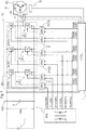
以下、回転電機駆動装置に適用される形態を例として駆動電源装置の実施形態を図面に基づいて説明する。図1の回路ブロック図は、回転電機駆動装置100のシステム構成を模式的に示している。回転電機駆動装置100は、直流電源11(高圧直流電源)に接続されて直流電力と複数相の交流電力との間で電力を変換するインバータ10を介して回転電機80を駆動する。図1に示すように、インバータ10は、上段側スイッチング素子3Hと下段側スイッチング素子3Lとの直列回路により構成された交流1相分のアーム3Aを複数本(ここでは3本)備えている。インバータ10は、直流電力を複数相(nを自然数としてn相、ここでは3相)の交流電力に変換して回転電機80に供給する。本実施形態では、回転電機80のU相、V相、W相に対応するステータコイル8のそれぞれに一組の直列回路(アーム3A)が対応したブリッジ回路としてインバータ10が構成されている。
Hereinafter, embodiments of the drive power supply device will be described with reference to the drawings, taking as an example the embodiment applied to the rotary electric machine drive device. The circuit block diagram of FIG. 1 schematically shows the system configuration of the rotary electric
尚、回転電機80は、発電機として機能してもよい。回転電機80が発電機としても機能する場合には、回転電機80が発電した交流電力を直流電力に変換して直流電源11に供給する。直流電源11は、ニッケル水素電池やリチウムイオン電池などの二次電池(バッテリ)や、電気二重層キャパシタなどにより構成されていると好適である。
The rotary
回転電機80は、例えばハイブリッド自動車や電気自動車等の車両の駆動力源とすることができる。回転電機80が車両の駆動力源の場合、インバータ10の直流側の電圧(直流リンク電圧Vdc)は、例えば200〜400ボルトである。インバータ10の直流側には、回転電機80の消費電力の変動に応じて変動する直流リンク電圧Vdcを平滑化する平滑コンデンサ(直流リンクコンデンサ4)が備えられている。
The rotary
図1に示すように、インバータ10は、複数のスイッチング素子3を有して構成される。スイッチング素子3には、IGBT(Insulated Gate Bipolar Transistor)やパワーMOSFET(Metal Oxide Semiconductor Field Effect Transistor)やSiC−MOSFET(Silicon Carbide - Metal Oxide Semiconductor FET)やSiC−SIT(SiC - Static Induction Transistor)、GaN−MOSFET(Gallium Nitride - MOSFET)などのパワー半導体素子を適用すると好適である。図1に示すように、本実施形態では、スイッチング素子3としてIGBTが用いられる形態を例示している。尚、各スイッチング素子3には、負極から正極へ向かう方向(下段側から上段側へ向かう方向)を順方向として、不図示のフリーホイールダイオードが、スイッチング素子3に対して並列に備えられている。
As shown in FIG. 1, the
インバータ10は、インバータ制御装置(CTRL)1により制御される。インバータ制御装置1は、マイクロコンピュータ等の論理プロセッサを中核部材として構築されている。例えば、インバータ制御装置1は、不図示の車両ECUなどの他の制御装置から提供される回転電機80の目標トルクに基づいて、ベクトル制御法を用いた電流フィードバック制御を行って、インバータ10を介して回転電機80を制御する。回転電機80の各相のステータコイル8を流れる実電流は電流センサ14により検出され、インバータ制御装置1はその検出結果を取得する。また、回転電機80のロータの各時点での磁極位置や回転速度は、レゾルバなどの回転センサ15により検出され、インバータ制御装置1はその検出結果を取得する。
The
インバータ制御装置1は、電流センサ14及び回転センサ15の検出結果を用いて、例えばベクトル制御法を用いて電流フィードバック制御を実行する。インバータ制御装置1は、モータ制御のために種々の機能部を有して構成されており、各機能部は、マイクロコンピュータ等のハードウエアとソフトウエア(プログラム)との協働により実現される。ベクトル制御及び電流フィードバック制御については、公知であるのでここでは詳細な説明は省略する。
The inverter control device 1 executes current feedback control using, for example, a vector control method, using the detection results of the
ところで、インバータ10を構成するそれぞれのスイッチング素子3の制御端子(例えばIGBTのゲート端子)は、駆動回路(DRV)2を介してインバータ制御装置1に接続されており、それぞれ個別にスイッチング制御される。スイッチング制御信号SW(SW1〜SW6)を生成するインバータ制御装置1は、マイクロコンピュータなどを中核とした電子回路であり、低圧系回路として構成される。低圧系回路は、インバータ10などの高圧系回路とは、動作電圧(回路の電源電圧)が大きく異なる。多くの場合、車両には、直流電源11の他に、直流電源11よりも低電圧(例えば12ボルト〜24ボルト)の電源である低圧直流電源(不図示)も搭載されている。インバータ制御装置1の動作電圧は、例えば5ボルトや3.3ボルトであり、低圧直流電源の電力に基づいてこのような動作電圧を生成する不図示の電圧レギュレータなどの電源回路から電力を供給されて動作する。
By the way, the control terminals (for example, the gate terminals of the IGBTs) of the
上述したように、低圧系回路は、インバータ10などの高圧系回路とは、動作電圧(回路の電源電圧)が大きく異なる。このため、回転電機駆動装置100には、各スイッチング素子3に対するスイッチング制御信号SW(スイッチング素子3がMOSFETやIGBTの場合、ゲート駆動信号)の電力を増幅する駆動回路2が備えられている。換言すれば、駆動回路2は、スイッチング制御信号SWの駆動能力(例えば電圧振幅や出力電流など、後段の回路を動作させる能力)をそれぞれ高めて対応するスイッチング素子3に伝達する。
As described above, the low-voltage circuit has a significantly different operating voltage (power supply voltage of the circuit) from the high-voltage circuit such as the
駆動回路2は、それぞれのスイッチング素子3に対応して備えられている。図1に示すように、本実施形態では、インバータ10に、駆動対象となる6つのスイッチング素子3が備えられており、駆動回路2も6つ備えられている。駆動回路2には、上段側スイッチング素子3Hにスイッチング制御信号SWを伝達する上段側駆動回路2Hと、下段側スイッチング素子3Lにスイッチング制御信号SWを伝達する下段側駆動回路2Lとがあるが、特に区別する必要が無い場合は、単に駆動回路2として説明する。
The
駆動回路2には低圧系回路よりも高い動作電圧が必要である。駆動回路2に電力を供給するために、駆動電源回路(PW)7(駆動電源装置)が設けられている。図2は、駆動電源回路7の一例を示している。6つのスイッチング素子3及び6つの駆動回路2に対応して、駆動電源回路7は6つのトランスLを備えている。具体的には、駆動電源回路7は、3つの上段用トランスLH(U相上段用トランスL1、V相上段用トランスL3、W相上段用トランスL5)と、3つの下段用トランスLL(U相下段用トランスL2、V相下段用トランスL4、W相下段用トランスL6)とを有している。各トランス(L1〜L6)は同じ構成であり、ほぼ同電圧の二次電圧(出力電圧V2)が出力される(U相上段用駆動電圧VHU,U相下段用駆動電圧VLU,V相上段用駆動電圧VHV,V相下段用駆動電圧VLV,W相上段用駆動電圧VHW,W相下段用駆動電圧VLW)。各相の上段用駆動電圧及び下段用駆動電圧を総称する場合は、上段用駆動電圧VH及び下段用駆動電圧VLと称する。
The
尚、各トランスLの一次側の入力電圧V1は、電圧レギュレータ等によって安定化された電源回路から供給されているので、二次側の出力電圧V2を一次側にフィードバックすることなく、トランスLの変圧比によって二次側の出力電圧V2が決定されている。また、D1〜D12は二次側コイルLsに生じる交流を整流する整流用ダイオード、C1〜C6は整流後の波形を平滑する平滑コンデンサである。 Since the input voltage V1 on the primary side of each transformer L is supplied from the power supply circuit stabilized by a voltage regulator or the like, the output voltage V2 on the secondary side is not fed back to the primary side of the transformer L. The output voltage V2 on the secondary side is determined by the transformation ratio. Further, D1 to D12 are rectifying diodes for rectifying alternating current generated in the secondary coil Ls, and C1 to C6 are smoothing capacitors for smoothing the waveform after rectification.
各トランスLの一次側コイルLpは低圧系回路LVに属し、二次側コイルLsは高圧系回路HVに属している。つまり、トランスLは、低圧系回路LVと高圧系回路HVとの境界部分に配置され、絶縁状態で低圧系回路LVと高圧系回路HVとを接続している(図6参照)。尚、駆動回路2も、図6に示すように、光によって信号を伝達するフォトカプラや磁気によって信号を伝達する磁気カプラなど、電気的に絶縁された状態で信号を伝達する絶縁素子21を備えている。この絶縁素子21も、低圧系回路LVと高圧系回路HVとの境界部分に配置されている。
The primary side coil Lp of each transformer L belongs to the low voltage system circuit LV, and the secondary side coil Ls belongs to the high voltage system circuit HV. That is, the transformer L is arranged at the boundary between the low-voltage circuit LV and the high-voltage circuit HV, and connects the low-voltage circuit LV and the high-voltage circuit HV in an insulated state (see FIG. 6). As shown in FIG. 6, the
図2に示すように、一次側コイルLpには、一次側コイルLpに印加される電圧をスイッチングする駆動用スイッチング素子Mが接続されている。ここでは、プッシュプル型のスイッチング電源回路を例示しており、一次側コイルLpには相補的にスイッチング制御される2つの駆動用スイッチング素子M(第1スイッチング素子51,第2スイッチング素子52)が接続されている。これらの駆動用スイッチング素子M(第1スイッチング素子51,第2スイッチング素子52)は、電源制御回路(PW-CTRL)6によってスイッチング制御される。図2に示すように、本実施形態では、第1スイッチング素子51及び第2スイッチング素子52の2つの駆動用スイッチング素子Mを有して、一次側コイルLpへの電力の供給を制御するトランス駆動ユニット5が構成されている。
As shown in FIG. 2, a drive switching element M for switching the voltage applied to the primary coil Lp is connected to the primary coil Lp. Here, a push-pull type switching power supply circuit is illustrated, and two drive switching elements M (first switching
本実施形態では、3相交流の各相に対応して、6つのトランスLが、3組のトランス対に組分けされている。つまり、U相に対応するトランス対(L1,L2)、V相に対応するトランス対(L3,L4)、W相に対応するトランス対(L5,L6)である。それぞれのトランス対は、共通のトランス駆動ユニット5(駆動用スイッチング素子M)によって駆動される。U相に対応するトランス対(L1,L2)は、U相第1スイッチング素子M1及びU相第2スイッチング素子M2によって、V相に対応するトランス対(L3,L4)は、V相第1スイッチング素子M3及びV相第2スイッチング素子M4によって、W相に対応するトランス対(L5,L6)は、W相第1スイッチング素子M5及びW相第2スイッチング素子M6によって駆動される。 In the present embodiment, six transformers L are grouped into three sets of transformer pairs corresponding to each phase of three-phase alternating current. That is, the transformer pair (L1, L2) corresponding to the U phase, the transformer pair (L3, L4) corresponding to the V phase, and the transformer pair (L5, L6) corresponding to the W phase. Each transformer pair is driven by a common transformer drive unit 5 (drive switching element M). The transformer pair (L1, L2) corresponding to the U phase is the U-phase first switching element M1 and the U-phase second switching element M2, and the transformer pair (L3, L4) corresponding to the V phase is the V-phase first switching. The transformer pair (L5, L6) corresponding to the W phase is driven by the W phase first switching element M5 and the W phase second switching element M6 by the element M3 and the V phase second switching element M4.
上述したように、トランス駆動ユニット5の一対の駆動用スイッチング素子M、即ち、第1スイッチング素子51と第2スイッチング素子52(それぞれM1とM2との対、M3とM4との対、M5とM6との対)は、相補的にスイッチング制御される。図3の波形図には、各駆動用スイッチング素子Mをスイッチング制御するトランス駆動信号MGを模式的に示している。M1GはU相第1スイッチング素子M1を駆動するU相第1スイッチング素子駆動信号であり、M2GはU相第2スイッチング素子M2を駆動するU相第2スイッチング素子駆動信号である。以下、M3G,M4G,M5G,M6Gは、それぞれ、V相第1スイッチング素子M3、V相第2スイッチング素子M4、W相第1スイッチング素子M5、W相第2スイッチング素子M6を駆動するトランス駆動信号であり、順に、V相第1スイッチング素子駆動信号、V相第2スイッチング素子駆動信号、W相第1スイッチング素子駆動信号、W相第2スイッチング素子駆動信号である。
As described above, the pair of drive switching elements M of the
U相第1スイッチング素子駆動信号M1Gに対してU相第2スイッチング素子駆動信号M2Gは、論理が反転している。U相第1スイッチング素子駆動信号M1Gを正転信号とすると、U相第2スイッチング素子駆動信号M2Gは反転信号である。つまり、U相第1スイッチング素子駆動信号M1GとU相第2スイッチング素子駆動信号M2Gとは、位相が180°異なる正反一対のトランス駆動信号MGである。同様に、V相第1スイッチング素子駆動信号M3G及びV相第2スイッチング素子駆動信号M4Gも互いに論理が反転しており、位相が180°異なる正反一対のトランス駆動信号MGである。また、W相第1スイッチング素子駆動信号M5G及びW相第2スイッチング素子駆動信号M6Gも互いに論理が反転しており、位相が180°異なる正反一対のトランス駆動信号MGである。 The logic of the U-phase second switching element drive signal M2G is inverted with respect to the U-phase first switching element drive signal M1G. Assuming that the U-phase first switching element drive signal M1G is a forward rotation signal, the U-phase second switching element drive signal M2G is an inverting signal. That is, the U-phase first switching element drive signal M1G and the U-phase second switching element drive signal M2G are a pair of forward and reverse transformer drive signals MG having different phases by 180 °. Similarly, the V-phase first switching element drive signal M3G and the V-phase second switching element drive signal M4G are also pair of forward and reverse transformer drive signals MG whose logics are inverted from each other and whose phases differ by 180 °. Further, the W-phase first switching element drive signal M5G and the W-phase second switching element drive signal M6G are also pair of forward and reverse transformer drive signals MG whose logics are inverted from each other and whose phases differ by 180 °.
U相第1スイッチング素子駆動信号M1GとV相第1スイッチング素子駆動信号M3Gとは、位相が120°異なっており、V相第1スイッチング素子駆動信号M3GとW相第1スイッチング素子駆動信号M5Gとも、位相が120°異なっており、さらにW相第1スイッチング素子駆動信号M5GとU相第1スイッチング素子駆動信号M1Gとも、位相が120°異なっている。同様に、U相第2スイッチング素子駆動信号M2GとV相第2スイッチング素子駆動信号M4Gとは、位相が120°異なっており、V相第2スイッチング素子駆動信号M4GとW相第2スイッチング素子駆動信号M6Gとも、位相が120°異なっており、さらにW相第2スイッチング素子駆動信号M6GとU相第2スイッチング素子駆動信号M2Gとも、位相が120°異なっている。 The U-phase first switching element drive signal M1G and the V-phase first switching element drive signal M3G are different in phase by 120 °, and both the V-phase first switching element drive signal M3G and the W-phase first switching element drive signal M5G The phases are different by 120 °, and the phases of the W-phase first switching element drive signal M5G and the U-phase first switching element drive signal M1G are also different by 120 °. Similarly, the U-phase second switching element drive signal M2G and the V-phase second switching element drive signal M4G are 120 ° out of phase, and the V-phase second switching element drive signal M4G and the W-phase second switching element drive are driven. The phases of the signal M6G are also different by 120 °, and the phases of the W-phase second switching element drive signal M6G and the U-phase second switching element drive signal M2G are also different by 120 °.
本実施形態では、駆動電源回路7は、変化点が共通する正反一対のトランス駆動信号によって相補的にスイッチング制御される第1スイッチング素子51と第2スイッチング素子52との一対の駆動用スイッチング素子Mを有したトランス駆動ユニット5を3組有している。そして、それぞれの組のトランス駆動ユニット5は、120°(=360°/3組)ずつ位相が異なる3種類の正反一対のトランス駆動信号によって駆動される。つまり、U相第1スイッチング素子駆動信号M1G及びU相第2スイッチング素子駆動信号M2Gによる正反一対のトランス駆動信号MGと、V相第1スイッチング素子駆動信号M3G及びV相第2スイッチング素子駆動信号M4Gによる正反一対のトランス駆動信号MGと、W相第1スイッチング素子駆動信号M5G及びW相第2スイッチング素子駆動信号M6Gによる正反一対のトランス駆動信号MGとは、120°(=360°/3組)ずつ位相が異なっている。
In the present embodiment, the drive
このように、駆動電源回路7は、一次側コイルLpと、この一次側コイルLpと電気的に絶縁状態で結合する二次側コイルLsとを有し、二次側コイルLsがそれぞれの駆動回路2に個別に接続される複数のトランスLを有して構成されている。また、それぞれのトランスLの一次側コイルLpには、それぞれの一次側コイルLpへの電力の供給を制御する駆動用スイッチング素子Mを有する複数のトランス駆動ユニット5が接続されている。電源制御装置6は、それぞれのトランス駆動ユニット5を駆動するトランス駆動信号MGを、互いに異なる位相で提供している。
As described above, the drive
図2及び図3を参照して例示したように、本実施形態では、変化点が共通するトランス駆動信号MG(それぞれ、M1GとM2G,M3GとM4G,M5GとM6G)によって駆動されるトランス駆動ユニット5の組をm個(mは2以上の自然数、ここではm=3)有している。それぞれの組のトランス駆動ユニット5は、電気角一周期の位相(360°)を組数m(ここでは3)で除した位相(=120°)ずつ、位相が異なるトランス駆動信号MGによって駆動される。尚、本実施形態では、3つのトランス駆動ユニット5を備え、それぞれ1つのトランス駆動ユニット5により、1つのトランス駆動ユニット5の組が構成されている形態を例示している。当然ながら、複数のトランス駆動ユニット5により、1つのトランス駆動ユニット5の組が構成されていてもよい。例えば、6つのトランス駆動ユニット5を備え、それぞれ2つのトランス駆動ユニット5により、1つのトランス駆動ユニット5の組が構成されて、3つの組を有する形態であってもよい。
As illustrated with reference to FIGS. 2 and 3, in the present embodiment, a transformer drive unit driven by a transformer drive signal MG (M1G and M2G, M3G and M4G, M5G and M6G, respectively) having a common change point. It has m sets of 5 (m is a natural number of 2 or more, here m = 3). Each set of
本実施形態では、3相交流(n相交流)の各相に対応して、6つのトランスLが、3組(m組)のトランス対に組分けされている(m=n)。従って、各相に対応するそれぞれのトランス駆動ユニット5(M1及びM2のユニット,M3及びM4のユニット,M5及びM6のユニット)は、それぞれ電気角一周期の位相(360°)を相数n(ここでは3)で除した位相差(=120°)を有するトランス駆動信号MGによって駆動されるということもできる。或は、相数nを組数mとして組分けを行うということもできる。 In the present embodiment, six transformers L are grouped into three sets (m sets) of transformer pairs corresponding to each phase of three-phase alternating current (n-phase alternating current) (m = n). Therefore, each transformer drive unit 5 (unit of M1 and M2, unit of M3 and M4, unit of M5 and M6) corresponding to each phase has a phase (360 °) of one electrical angle cycle with n (360 °) of phases. Here, it can also be said that it is driven by a transformer drive signal MG having a phase difference (= 120 °) divided by 3). Alternatively, it is also possible to perform grouping with the number of phases n as the number of groups m.
このように、複数のトランスLが、互いに異なる位相のトランス駆動信号MGによって駆動されると、図3に示すように、一次側の入力電流Iddに電流リップルが生じるタイミングが、それぞれのトランスLによって異なるようになる。つまり、入力電流Iddが脈動するタイミングが分散することによって、入力電流Iddのリップルの最大波高値I1(ピーク・トゥ・ピーク)が小さくなる。従って、複数のトランスLを用いた駆動電源回路7の一次側の電流リップルの最大振幅を低減することができる。その結果、例えば、入力電流Iddのリップルを吸収して一次側の電圧を平滑化するフィルタコンデンサCfなどを用いたフィルタ回路の規模も小さくすることができる。
In this way, when a plurality of transformers L are driven by transformer drive signals MG having different phases, as shown in FIG. 3, the timing at which current ripple occurs in the input current Idd on the primary side is determined by each transformer L. Will be different. That is, the timing at which the input current Idd pulsates is dispersed, so that the maximum peak value I1 (peak to peak) of the ripple of the input current Idd becomes smaller. Therefore, the maximum amplitude of the current ripple on the primary side of the drive
以下、比較例の駆動電源回路70も参照して説明する。図4の回路ブロック図は、比較例の駆動電源回路70を模式的に示している。また、図5の波形図は、比較例の駆動電源回路70を制御するトランス駆動信号MGと入力電流Iddとの関係を示している。本実施形態の駆動電源回路7と同様の構成については同様の参照符号を付し、適宜説明を省略する。図4に示すように、比較例では、トランスLを複数の組に組分けすることなく、6つ全てのトランスLを同じトランス駆動ユニット5を介して駆動している。従って、図5に示すように、全てのトランスLに対してトランス駆動信号MGは位相が同じ信号となる。
Hereinafter, the drive
比較例の駆動電源回路70の場合、複数のトランスLが、同じ位相のトランス駆動信号MGによって駆動される。このため、図5に示すように、入力側において入力電流Iddが脈動するタイミングが、それぞれのトランスLによって異ならず、全て同じタイミングとなる。その結果、入力電流Iddが脈動するタイミングが分散せず、電流リップルの最大波高値I3は、図3に例示した最大波高値I1に対して大きくなる。本実施形態では、入力電流Iddが脈動するタイミングを3回に分散させたことにより、このタイミングが集中する比較例に比べて、最大波高値I1が1/3となっている(I1=I3/3)。
In the case of the drive
本実施形態では最大波高値が比較例に比べて1/3となることにより、一次側の電圧を平滑化するフィルタコンデンサCfの容量を低減することができ、回路規模も小さくすることができる。尚、電流リップルの周波数は、図3と図5との比較から明らかなように、本実施形態では比較例の3倍となっている。しかし、フィルタ回路をコンデンサによって構成する場合、そのインピーダンスは、周波数に反比例する(周波数をfとしてインピーダンスは“1/2πf”)。つまり、周波数が高くなるとインピーダンスが低下するため、よりリップル成分を吸収し易くなる。 In the present embodiment, since the maximum peak value is 1/3 of that of the comparative example, the capacitance of the filter capacitor Cf that smoothes the voltage on the primary side can be reduced, and the circuit scale can also be reduced. As is clear from the comparison between FIGS. 3 and 5, the frequency of the current ripple is three times that of the comparative example in this embodiment. However, when the filter circuit is composed of capacitors, its impedance is inversely proportional to the frequency (the impedance is "1 / 2πf" with the frequency as f). That is, as the frequency increases, the impedance decreases, so that it becomes easier to absorb the ripple component.
ところで、上記においては、トランスLを3組に組分けする形態を例示したが、当然ながら組の数(m)は、3に限定されるものではない。例えば、上段用トランスLHの組と、下段用トランスLLの組との2組に分けてもよい。また、6つ全てのトランスLを異なる組として、6組に分けてもよい。 By the way, in the above, the mode in which the transformer L is grouped into three sets is illustrated, but the number of sets (m) is not limited to three as a matter of course. For example, it may be divided into two sets, a set of upper transformer LH and a set of lower transformer LL. Further, all six transformers L may be set as different sets and divided into six sets.
但し、組数mが2や6の場合は、上述したように組数mが3の場合に比べて注意が必要である。上述したように、相補的にスイッチング制御される2つの駆動用スイッチング素子Mの一方のトランス駆動信号MG(例えばU相第1スイッチング素子駆動信号M1G)に対して、他方のトランス駆動信号MG(例えばU相第2スイッチング素子駆動信号M2G)は論理が反転している。これら正反一対のトランス駆動信号MGの位相は、互いに180°ずれているということができる。ここで、“360°/m”で求められる位相差が180°の約数となる位相の場合には、位相のずれが180°となるトランス駆動信号MGが発生することになる。 However, when the number of sets m is 2 or 6, care must be taken as compared with the case where the number of sets m is 3 as described above. As described above, for one transformer drive signal MG (for example, U-phase first switching element drive signal M1G) of the two drive switching elements M that are complementarily controlled for switching, the other transformer drive signal MG (for example, for example). The logic of the U-phase second switching element drive signal M2G) is inverted. It can be said that the phases of the pair of positive and negative transformer drive signals MG are 180 ° out of phase with each other. Here, in the case where the phase difference obtained at "360 ° / m" is a divisor of 180 °, a transformer drive signal MG having a phase shift of 180 ° is generated.
例えば、トランスLを2組に分けた場合(m=2)を考える。便宜的にここでは、M1G及びM2Gを、3つの上段用トランスLHを駆動するトランス駆動ユニット5の正反一対のトランス駆動信号MGとし、M3G及びM4Gを、3つの下段用トランスLLを駆動するトランス駆動ユニット5の正反一対のトランス駆動信号MGとする。m=3の場合と同じように、M1G及びM2Gの対と、M3G及びM4Gの対との位相差を180°(360°/2)とすると、図7の波形図に示すように、M2GとM3Gとの位相が同一となってしまう。
For example, consider the case where the transformer L is divided into two sets (m = 2). For convenience, here, M1G and M2G are a pair of forward and reverse transformer drive signals MG of the
ここで、図8の波形図に示すように、M1G及びM2Gの対と、M3G及びM4Gの対との位相差を90°とすると、図8の波形図に示すように、M1G、M2G、M3G、M4Gが全て異なる位相となる。また、M1G、M2G、M3G、M4Gの位相差は、均等である。従って、“360/m”が180の約数である場合は、複数の正反一対のトランス駆動信号MGの位相を、180°の範囲内で異ならせることが好ましい。具体的には、“360/m”が180の約数である場合は、それぞれの組のトランス駆動ユニット5は、“180°/m”ずつ位相が異なる正反一対のトランス駆動信号MGによって駆動されると好適である。
Here, assuming that the phase difference between the pair of M1G and M2G and the pair of M3G and M4G is 90 ° as shown in the waveform diagram of FIG. 8, M1G, M2G, and M3G are shown in the waveform diagram of FIG. , M4G are all in different phases. Further, the phase differences of M1G, M2G, M3G, and M4G are equal. Therefore, when "360 / m" is a divisor of 180, it is preferable to make the phases of the plurality of pairs of positive and negative transformer drive signals MG different within a range of 180 °. Specifically, when "360 / m" is a divisor of 180, each set of
m=2の場合には、位相差は“180°/2=90°”となり、図7及び図8を参照して検証した結果と良好に一致する。図示等は省略するが、6組に分けた場合(m=6)の場合も、“360/6=60”が180の約数であるため、位相差を“180°/6=30°”とすることが好ましい。“360/m”が180の約数となる組数mは、m=2,6の他、m=4,8,16などmが2のべき乗である場合や、m=10,12,18などである。 When m = 2, the phase difference is “180 ° / 2 = 90 °”, which is in good agreement with the results verified with reference to FIGS. 7 and 8. Although not shown, the phase difference is "180 ° / 6 = 30 °" because "360/6 = 60" is a divisor of 180 even when divided into 6 groups (m = 6). Is preferable. The number of pairs m in which "360 / m" is a divisor of 180 is m = 2,6, m = 4,8,16, etc., when m is a power of 2, or m = 10,12,18. And so on.
尚、図8に示す形態(m=2)では、M1G及びM2Gの対に対して、M3G及びM4Gの対の位相が90°遅れている。一方、視点を変えると、M3G及びM4Gの対に対して、M1G及びM2Gの対の位相が270°遅れているということもできる。しかし、M1G及びM2Gの対から見て、M3G及びM4Gの対の位相は90°異なっており(この場合、遅れており)、M3G及びM4Gの対から見て、M1G及びM2Gの対の位相も90°異なっている(この場合、進んでいる)ため、それぞれの組のトランス駆動ユニット5は、“(180°/m)=90°”ずつ位相が異なる正反一対のトランス駆動信号MGによって駆動されるということができる。
In the embodiment (m = 2) shown in FIG. 8, the phase of the pair of M3G and M4G is delayed by 90 ° with respect to the pair of M1G and M2G. On the other hand, when the viewpoint is changed, it can be said that the phase of the pair of M1G and M2G is delayed by 270 ° with respect to the pair of M3G and M4G. However, when viewed from the M1G and M2G pairs, the phases of the M3G and M4G pairs differ by 90 ° (in this case, they are delayed), and when viewed from the M3G and M4G pairs, the phases of the M1G and M2G pairs also differ. Since they differ by 90 ° (in this case, they are advanced), each set of
また、例えば、m=4の場合には、同様に位相の遅れ及び進みを、45°(=180°/4)により表現することができる。例えば、第1の組の正反一対のトランス駆動信号MGに対して第2の組の正反一対のトランス駆動信号MGは45°位相が遅れ、第2の組の正反一対のトランス駆動信号MGに対して第3の組の正反一対のトランス駆動信号MGは45°位相が遅れ、第3の組の正反一対のトランス駆動信号MGに対して第4の組の正反一対のトランス駆動信号MGは45°位相が遅れる。第4の組の正反一対のトランス駆動信号MGに対して第1の組の正反一対のトランス駆動信号MGは、225°位相が遅れる又は135°位相が進んでいるといえる。しかし、第1の組、第2の組、第3の組、第4の組の順に考えると、正反一対のトランス駆動信号MGの位相が45°ずつ遅れており(異なっており)、第4の組、第3の組、第2の組、第1の組の順に考えると、正反一対のトランス駆動信号MGの位相が45°ずつ進んでいる(異なっている)。従って、m=2の場合と同様に、それぞれの組のトランス駆動ユニット5は、“(180°/m)=45°”ずつ位相が異なる正反一対のトランス駆動信号MGによって駆動されるということができる。詳細な説明は省略するが、m=6,8,16,0,12,18等についても同様である。
Further, for example, in the case of m = 4, the phase delay and advance can be similarly expressed by 45 ° (= 180 ° / 4). For example, the first set of positive and negative pairs of transformer drive signals MG and the second set of positive and negative pairs of transformer drive signals MG are 45 ° out of phase, and the second set of positive and negative pairs of transformer drive signals The third set of positive and negative transformer drive signals MG is 45 ° out of phase with respect to MG, and the fourth set of positive and negative transformers is relative to the third set of positive and negative transformer drive signals MG. The drive signal MG is 45 ° out of phase. It can be said that the first set of positive and negative pairs of transformer drive signals MG is 225 ° out of phase or 135 ° out of phase with respect to the fourth set of positive and negative pairs of transformer drive signals MG. However, considering the order of the first set, the second set, the third set, and the fourth set, the phases of the pair of forward and reverse transformer drive signals MG are delayed by 45 ° (different), and the first set. Considering the order of 4, the third set, the second set, and the first set, the phases of the pair of forward and reverse transformer drive signals MG are advanced by 45 ° (different). Therefore, as in the case of m = 2, each set of
ところで、図2等を参照して上述したように、本実施形態では、3相交流の各相に対応して、6つのトランスLが、3組のトランス対(L1及びL2の対、L3及びL4の対、L5及びL6の対)に組分けされている。それぞれのトランス対は、それぞれ異なるトランス駆動ユニット5(駆動用スイッチング素子M)によって制御される。U相に対応するトランス対(L1,L2)は、U相第1スイッチング素子M1及びU相第2スイッチング素子M2によって、V相に対応するトランス対(L3,L4)は、V相第1スイッチング素子M3及びV相第2スイッチング素子M4によって、W相に対応するトランス対(L5,L6)は、W相第1スイッチング素子M5及びW相第2スイッチング素子M6によって制御される。 By the way, as described above with reference to FIG. 2 and the like, in the present embodiment, six transformers L correspond to each phase of three-phase alternating current, and three sets of transformer pairs (L1 and L2 pairs, L3 and It is grouped into pairs of L4 and pairs of L5 and L6). Each transformer pair is controlled by a different transformer drive unit 5 (drive switching element M). The transformer pair (L1, L2) corresponding to the U phase is the U-phase first switching element M1 and the U-phase second switching element M2, and the transformer pair (L3, L4) corresponding to the V phase is the V-phase first switching. The transformer pair (L5, L6) corresponding to the W phase is controlled by the W phase first switching element M5 and the W phase second switching element M6 by the element M3 and the V phase second switching element M4.
各相のアーム3Aを構成する上段側スイッチング素子3Hと下段側スイッチング素子3Lとは、一般的に近傍に配置される。図9は、駆動電源回路7及び駆動回路2の基板上における配置例を示している。各相の上段側スイッチング素子3Hと下段側スイッチング素子3Lとは近接して、高圧系回路HVの配置領域に配置されている。各相に対応するトランスLは、他の相には電力を供給しないため、当該相の近傍に配置することができる。また、当該相のトランスLは、他の相に電力を供給するトランスLとは異なる駆動用スイッチング素子M(トランス駆動ユニット5)によって駆動される。従って、図9に示すように、各相に対応するトランスLと、そのトランスLに対する駆動用スイッチング素子M(トランス駆動ユニット5)とを近接させて基板9上に配置することができる。
The
その結果、駆動用スイッチング素子M(トランス駆動ユニット5)と、トランスLとの配線(図9において2つの駆動用スイッチング素子M(M1,M2)から延びる実線及び破線)を短くすることができる。この配線上には、入力電流Iddの脈動が伝搬する。このため、基板9上の配線からリップル成分に起因する電磁ノイズが放射される可能性があるが、配線長が長い場合に比べて配線長が短いと電磁ノイズの放射が低減される。 As a result, the wiring between the drive switching element M (transformer drive unit 5) and the transformer L (solid lines and broken lines extending from the two drive switching elements M (M1, M2) in FIG. 9) can be shortened. The pulsation of the input current Idd propagates on this wiring. Therefore, electromagnetic noise due to the ripple component may be radiated from the wiring on the substrate 9, but when the wiring length is short as compared with the case where the wiring length is long, the radiation of electromagnetic noise is reduced.
図10は、図5に例示した比較例の駆動電源回路70及び駆動回路2の基板上における配置例を示している。比較例の駆動電源回路70でも、各相に対応するトランスLは、他の相には電力を供給しないため、当該相の近傍に配置することができる。しかし、当該相のトランスLは、他の相に電力を供給するトランスLと同じ駆動用スイッチング素子M(トランス駆動ユニット5)によって駆動される。従って、駆動用スイッチング素子M(トランス駆動ユニット5)と、トランスLとの配線(図10において2つの駆動用スイッチング素子M(M1,M2)から延びる実線及び破線)は、全てのトランスLに対して引き回されることになり、配線長が長くなる傾向がある。図9と図10との比較により明らかなように、駆動用スイッチング素子M(トランス駆動ユニット5)と、トランスLとの配線長は、比較例の方が長い。配線長が長い場合には、リップル成分に起因する電磁ノイズが基板9上の配線からより多く放射される可能性がある。
FIG. 10 shows an example of arrangement of the drive
尚、駆動電源回路7及び駆動回路2の基板上における配置例は、図9に例示したように、インバータ10を構成するスイッチング素子3が一列に並ぶような形態に限定されるものではない。例えば、図11に例示するように、交流の相ごとに分割して配置されていてもよい。6つのトランスLが、3相交流の各相に対応して組分けされ、それぞれの組がそれぞれ異なるトランス駆動ユニット5(駆動用スイッチング素子M)によって制御される場合には、このように交流の相ごとに分割してスイッチング素子3が配置されても駆動用スイッチング素子M(トランス駆動ユニット5)と、トランスLとの配線長を短くすることができる。
The arrangement example of the drive
また、図9に例示するような形態及び図11に例示するような形態の双方において、複数相全ての相についてトランスLと駆動用スイッチング素子M(トランス駆動ユニット5)とが近接配置されていなくてもよい。複数相の内、少なくとも1相だけであってもトランスLと駆動用スイッチング素子M(トランス駆動ユニット5)とが近接配置されていれば、電磁ノイズを低減する効果を得ることができる。 Further, in both the form illustrated in FIG. 9 and the form illustrated in FIG. 11, the transformer L and the driving switching element M (transformer driving unit 5) are not arranged in close proximity to all the phases of the plurality of phases. You may. If the transformer L and the drive switching element M (transformer drive unit 5) are arranged close to each other even if only one of the plurality of phases is used, the effect of reducing electromagnetic noise can be obtained.
〔その他の実施形態〕
以下、その他の実施形態について説明する。尚、以下に説明する各実施形態の構成は、それぞれ単独で適用されるものに限られず、矛盾が生じない限り、他の実施形態の構成と組み合わせて適用することも可能である。[Other Embodiments]
Hereinafter, other embodiments will be described. It should be noted that the configurations of the respective embodiments described below are not limited to those applied independently, and can be applied in combination with the configurations of other embodiments as long as there is no contradiction.
(1)上記においては、駆動電源回路7がプッシュプル方式のスイッチング電源として構成されている形態を例示した。しかし、駆動電源回路7は、その他の方式、例えば、ハーフブリッジ方式やフルブリッジ方式のスイッチング電源であってもよい。
(1) In the above, the embodiment in which the drive
(2)また、駆動電源回路7の方式は、プッシュプル方式、ハーフブリッジ方式、フルブリッジ方式などのように、トランスLを駆動するトランス駆動ユニット5が相補的にスイッチング制御される複数の駆動用スイッチング素子Mを有する方式に限るものでもない。駆動電源回路7は、トランス駆動ユニット5が単一の駆動用スイッチング素子Mにより構成されるシングルフォワード方式やフライバック方式のスイッチング電源であってもよい。尚、この場合には、当然ながら、トランス駆動ユニット5(駆動用スイッチング素子M)を駆動するトランス駆動信号MGは、正反一対ではなく単一の信号である。従って、トランスL及びトランス駆動ユニット5の組分けの数(組数m)に拘わらず、複数のトランス駆動信号MGの間に設定される位相差は、360°を組数mで除した値でよい。つまり、“360/m”が180の約数である場合も、約数ではない場合も、それぞれの組のトランス駆動ユニット5は、“360°/n”ずつ位相が異なるトランス駆動信号MGによって駆動される。
(2) Further, the drive
〔実施形態の概要〕
以下、上記において説明した駆動電源装置(7)の概要について簡単に説明する。[Outline of Embodiment]
Hereinafter, the outline of the drive power supply device (7) described above will be briefly described.
複数のスイッチング素子(3)を有して直流と複数相の交流との間で電力を変換するインバータ(10)のそれぞれの前記スイッチング素子(3)を個別に駆動する複数の駆動回路(2)に電力を供給する駆動電源装置(7)は、1つの態様として、一次側コイル(Lp)と当該一次側コイル(Lp)と電気的に絶縁状態で結合する二次側コイル(Ls)とを有し、前記二次側コイル(Ls)がそれぞれの前記駆動回路(2)に個別に接続される複数のトランス(L)と、それぞれの前記一次側コイル(Lp)に接続されてそれぞれの前記一次側コイル(Lp)への電力の供給を制御する駆動用スイッチング素子(M)を有する複数のトランス駆動ユニット(5)と、それぞれの前記トランス駆動ユニット(5)を駆動するトランス駆動信号(MG)を提供する電源制御装置(6)と、を備え、前記電源制御装置(6)が、それぞれの前記トランス駆動ユニット(5)を互いに異なる位相の前記トランス駆動信号(MG)で駆動する。 A plurality of drive circuits (2) that individually drive each of the switching elements (3) of an inverter (10) having a plurality of switching elements (3) and converting power between DC and a plurality of phases of AC. In one embodiment, the drive power supply device (7) that supplies power to the primary side coil (7) has a primary side coil (Lp) and a secondary side coil (Ls) that electrically couples the primary side coil (Lp) in an insulated state. A plurality of transformers (L) having the secondary coil (Ls) individually connected to the drive circuit (2), and each of the transformers (Lp) connected to the primary coil (Lp). A plurality of transformer drive units (5) having a drive switching element (M) for controlling the supply of power to the primary coil (Lp), and a transformer drive signal (MG) for driving each of the transformer drive units (5). The power supply control device (6) is provided, and the power supply control device (6) drives each of the transformer drive units (5) with the transformer drive signals (MG) having different phases from each other.
この構成によれば、複数のトランス(L)が、異なる位相のトランス駆動信号(MG)によって駆動されるので、入力側の電流(Idd)に電流リップルが生じるタイミングが、それぞれのトランス(L)によって異なる。電流リップルが生じるタイミングが分散することによって、電流リップルの最大振幅が小さくなる。即ち、本構成によれば、複数のトランス(L)を用いた電源装置の一次側の電流リップルの振幅を低減することができる。その結果、例えば、脈動を吸収して一次側の電圧を平滑化するコンデンサ(Cf)などを用いたフィルタ回路の規模も小さくすることができる。 According to this configuration, since a plurality of transformers (L) are driven by transformer drive signals (MG) having different phases, the timing at which current ripple occurs in the current (Id) on the input side is set for each transformer (L). Depends on. By dispersing the timing at which the current ripple occurs, the maximum amplitude of the current ripple becomes smaller. That is, according to this configuration, it is possible to reduce the amplitude of the current ripple on the primary side of the power supply device using the plurality of transformers (L). As a result, for example, the scale of the filter circuit using a capacitor (Cf) that absorbs the pulsation and smoothes the voltage on the primary side can be reduced.
ここで、変化点が共通する前記トランス駆動信号(MG)によって駆動される前記トランス駆動ユニット(5)の組をm個(mは2以上の自然数)有し、それぞれの組の前記トランス駆動ユニット(5)は、“360°/m”ずつ位相が異なる前記トランス駆動信号(MG)によって駆動されると好適である。 Here, there are m sets of the transformer drive units (5) driven by the transformer drive signal (MG) having a common change point (m is a natural number of 2 or more), and each set of the transformer drive units. (5) is preferably driven by the transformer drive signal (MG) whose phase is different by "360 ° / m".
変化点が共通するトランス駆動信号(MG)によって駆動されるトランス(L)は、同じタイミングで電流リップルを生じる。一方、変化点が異なるトランス駆動信号(MG)によって駆動されるトランス(L)は、それぞれ異なるタイミングで電流リップル(Idd)を生じる。異なるタイミングで生じる電流リップルのピーク(波高)のタイミングがずれているほど、電流リップルの最大振幅は小さくなる。本構成によれば、異なる組に属するトランス(L)が、均等な位相差を有し、異なる位相のトランス駆動信号(MG)によって駆動されるため、電流リップルの最大振幅が小さくなり、好適である。 The transformer (L) driven by the transformer drive signal (MG) having a common change point causes current ripple at the same timing. On the other hand, the transformers (L) driven by the transformer drive signals (MG) having different change points generate current ripples (Idd) at different timings. The greater the timing of the peaks (wave heights) of the current ripples that occur at different timings, the smaller the maximum amplitude of the current ripples. According to this configuration, the transformers (L) belonging to different sets have an equal phase difference and are driven by the transformer drive signals (MG) having different phases, so that the maximum amplitude of the current ripple becomes small, which is preferable. is there.
ここで、それぞれの前記トランス駆動ユニット(5)が、変化点が共通する正反一対の前記トランス駆動信号(MG)によって相補的にスイッチング制御される第1スイッチング素子(51(M1,M3,M5))と第2スイッチング素子(52(M2,M4,M6))との一対の前記駆動用スイッチング素子(M)を有する場合、それぞれの組の前記トランス駆動ユニット(5)が以下のように駆動されると好適である。即ち、“360/m”が180の約数である場合は、それぞれの組の前記トランス駆動ユニット(5)が、“180°/m”ずつ位相が異なる正反一対の前記トランス駆動信号(MG)によって駆動されると好適である。一方、“360/m”が180の約数以外の場合は、それぞれの組の前記トランス駆動ユニット(5)が、“360°/m”ずつ位相が異なる正反一対の前記トランス駆動信号(5)によって駆動されると好適である。 Here, the first switching element (51 (M1, M3, M5)) in which each of the transformer drive units (5) is selectively switched and controlled by a pair of positive and negative transformer drive signals (MG) having a common change point. )) And a pair of the driving switching elements (M) of the second switching element (52 (M2, M4, M6)), each set of the transformer drive unit (5) is driven as follows. It is preferable to be done. That is, when "360 / m" is a divisor of 180, the transformer drive units (5) of each set have a pair of forward and reverse transformer drive signals (MG) having different phases by "180 ° / m". ) Is preferred. On the other hand, when "360 / m" is other than a divisor of 180, the transformer drive units (5) of each set have a pair of forward and reverse transformer drive signals (5) having different phases by "360 ° / m". ) Is preferred.
相補的にスイッチング制御される2つの駆動用スイッチング素子(M)の一方のトランス駆動信号(MG)に対して、他方のトランス駆動信号(MG)は論理が反転している。つまり、相補的にスイッチング制御される2つの駆動用スイッチング素子(M)は、正転信号と反転信号との対である、正反一対のトランス駆動信号(MG)によってスイッチング制御される。これら正反一対のトランス駆動信号(MG)の位相は、互いに180°ずれているということができる。“360°/m”で求められる位相差が180°の約数となる位相の場合、位相のずれが180°となるトランス駆動信号(MG)が発生することになる。具体的には、1つの正反一対のトランス駆動信号(MG)の内の正転信号のトランス駆動信号(MG)と、他の正反一対のトランス駆動信号(MG)の内の反転信号のトランス駆動信号(MG)との位相が一致することになる。従って、“360/m”が180の約数である場合は、複数の正反一対のトランス駆動信号(MG)の位相を、180°の範囲内で異ならせることが好ましい。一方、“360/m”が180の約数以外の場合は、位相のずれが180°となるトランス駆動信号(MG)は発生しない。従って、“360/m”が180の約数以外の場合は、複数の正反一対のトランス駆動信号(MG)の位相を、360°の範囲内で異ならせることが好ましい。 The logic of one transformer drive signal (MG) of the two drive switching elements (M) that are complementarily controlled by switching is inverted with respect to the other transformer drive signal (MG). That is, the two drive switching elements (M) that are complementaryly switched and controlled are switched and controlled by a pair of forward and reverse transformer drive signals (MG) that are a pair of a forward rotation signal and an inversion signal. It can be said that the phases of the pair of positive and negative transformer drive signals (MG) are 180 ° out of phase with each other. When the phase difference obtained at "360 ° / m" is a divisor of 180 °, a transformer drive signal (MG) having a phase shift of 180 ° is generated. Specifically, the transformer drive signal (MG) of the forward rotation signal in one pair of positive and negative transformer drive signals (MG) and the inverted signal in the other pair of positive and negative transformer drive signals (MG) The phase with the transformer drive signal (MG) will match. Therefore, when "360 / m" is a divisor of 180, it is preferable to make the phases of a plurality of pairs of positive and negative transformer drive signals (MG) different within a range of 180 °. On the other hand, when "360 / m" is other than a divisor of 180, the transformer drive signal (MG) having a phase shift of 180 ° is not generated. Therefore, when "360 / m" is other than a divisor of 180, it is preferable to make the phases of a plurality of pairs of positive and negative transformer drive signals (MG) different within a range of 360 °.
ここで、前記インバータ(10)が、n相(nは2以上の自然数)の交流と直流との間で電力を変換するものであり、前記トランス駆動ユニット(5)の組数mがnであると好適である。 Here, the inverter (10) converts electric power between alternating current and direct current of n-phase (n is a natural number of 2 or more), and the number of sets m of the transformer drive unit (5) is n. It is preferable to have it.
変化点が共通する前記トランス駆動信号(MG)によって駆動されるトランス駆動ユニット(5)の組の数を、複数相の交流の相数と一致させると、組分けが容易である。一般的には、各相に対応するスイッチング素子(3)は近傍に配置されることも多いので、各相に対応して組分けを行うと基板上での配線も効率的となる。 When the number of sets of the transformer drive unit (5) driven by the transformer drive signal (MG) having a common change point is matched with the number of alternating current phases of a plurality of phases, the grouping is easy. In general, the switching element (3) corresponding to each phase is often arranged in the vicinity, and therefore, if the grouping is performed corresponding to each phase, the wiring on the substrate becomes efficient.
また、1つの態様として、前記インバータ(10)が、直流の正極側に接続された上段側スイッチング素子(3H)と直流の負極側に接続された下段側スイッチング素子(3L)との直列回路である交流1相分のアーム(3A)を複数本有し、それぞれの前記トランス駆動ユニット(5)が、相補的にスイッチング制御される第1スイッチング素子(51(M1,M3,M5))と第2スイッチング素子(52(M2,M4,M6))との一対の前記駆動用スイッチング素子(M)を有する場合、複数の前記トランス(L)の内、交流の同一相の前記アーム(3A)の上段側に対応する上段側トランス(LH)と下段側に対応する下段側トランス(LL)とが、共通の前記トランス駆動ユニット(5)により駆動され、前記上段側トランス(LH)の前記一次側コイル(Lp)の一端と前記下段側トランス(LL)の前記一次側コイル(Lp)の一端とが、前記第1スイッチング素子(51(M1,M3,M5))に接続され、前記上段側トランス(LH)の前記一次側コイル(Lp)の他端と前記下段側トランス(LL)の前記一次側コイル(Lp)の他端とが、前記第2スイッチング素子(52(M2,M4,M6))に接続されていると好適である。 Further, as one embodiment, the inverter (10) is a series circuit of an upper switching element (3H) connected to the positive side of direct current and a lower switching element (3L) connected to the negative side of direct current. A first switching element (51 (M1, M3, M5)) and a first switching element (51 (M1, M3, M5)) which have a plurality of arms (3A) for one AC phase and each of the transformer drive units (5) are complementaryly controlled for switching. When a pair of the driving switching elements (M) with two switching elements (52 (M2, M4, M6)) is provided, the arm (3A) having the same phase of alternating current among the plurality of transformers (L) The upper transformer (LH) corresponding to the upper side and the lower transformer (LL) corresponding to the lower side are driven by the common transformer drive unit (5), and the primary side of the upper transformer (LH) is driven. One end of the coil (Lp) and one end of the primary side coil (Lp) of the lower stage side transformer (LL) are connected to the first switching element (51 (M1, M3, M5)), and the upper stage side transformer. The other end of the primary side coil (Lp) of (LH) and the other end of the primary side coil (Lp) of the lower stage transformer (LL) are the second switching element (52 (M2, M4, M6)). ) Is preferably connected.
交流1相分のアーム(3A)の上段側スイッチング素子(3H)及び下段側スイッチング素子(3L)はインバータ(10)において互いに比較的近傍に配置される。従って、上段側トランス(LH)及び下段側トランス(LL)も互いに比較的近傍に配置される。第1スイッチング素子(51(M1,M3,M5))及び第2スイッチング素子(52(M2,M4,M6))も、上段側トランス(LH)及び下段側トランス(LL)の近傍に配置することができるので、トランス駆動ユニット(5)とトランス(L)との配線距離を短くすることができる。上述したように、トランス(L)の一次側には電流リップルが生じるが、配線が短くなることで脈動成分が伝搬する距離が短くなり、脈動成分に起因して発生する電磁ノイズも低減される。 The upper switching element (3H) and the lower switching element (3L) of the arm (3A) for one AC phase are arranged relatively close to each other in the inverter (10). Therefore, the upper transformer (LH) and the lower transformer (LL) are also arranged relatively close to each other. The first switching element (51 (M1, M3, M5)) and the second switching element (52 (M2, M4, M6)) shall also be arranged in the vicinity of the upper transformer (LH) and the lower transformer (LL). Therefore, the wiring distance between the transformer drive unit (5) and the transformer (L) can be shortened. As described above, current ripple occurs on the primary side of the transformer (L), but the shortened wiring shortens the propagation distance of the pulsating component and reduces the electromagnetic noise generated by the pulsating component. ..
また、1つの態様として、前記駆動回路(2)は、前記スイッチング素子(3)を駆動するスイッチング制御信号(SW)を生成する制御回路(1)を含む低電圧回路(LV)と前記インバータ(10)を含む高電圧回路(HV)とを電気的に絶縁して前記スイッチング制御信号(SW)を伝達する絶縁素子(51)を含み、交流の同一相の前記上段側トランス(LH)と前記下段側トランス(LL)とが、基板(9)上に隣接配置され、当該相の前記上段側スイッチング素子(3H)及び前記下段側スイッチング素子(3L)に対応するそれぞれの前記絶縁素子(51)が、前記上段側トランス(LH)と前記下段側トランス(LL)とを挟んで、並び方向の両側に配置されていると好適である。 Further, as one embodiment, the drive circuit (2) includes a low voltage circuit (LV) including a control circuit (1) for generating a switching control signal (SW) for driving the switching element (3) and the inverter (LV). The upper transformer (LH) having the same phase of AC and the upper transformer (LH) including an insulating element (51) that electrically insulates the high voltage circuit (HV) including 10) and transmits the switching control signal (SW). The lower transformer (LL) is arranged adjacent to the substrate (9), and the insulating element (51) corresponding to the upper switching element (3H) and the lower switching element (3L) of the phase. However, it is preferable that the upper transformer (LH) and the lower transformer (LL) are arranged on both sides in the arrangement direction.
上段側トランス(LH)と下段側トランス(LL)とが隣接配置されることによって、トランス駆動ユニット(5)とトランス(L)との配線距離を短くすることができる。また、トランス(L)は、駆動回路(2)に電力を供給するため、互いに近接して配置されることが好ましい。絶縁素子(51)を含む駆動回路(2)が、上段側トランス(LH)と下段側トランス(LL)とを挟んで並び方向の両側に配置されると、トランス(L)と駆動回路(2)とを近接配置することができる。また、トランス(L)は絶縁部品であり、例えば一次側コイル(Lp)が配置される低電圧回路(LV)と二次側コイル(Ls)が配置される高電圧回路(HV)とを電気的に絶縁した状態で接続することができる。トランス(L)と絶縁素子(51)とが、トランス(L)の並び方向に並んで配置されることで、低電圧回路(LV)と高電圧回路(HV)とを適切に絶縁すると共に、トランス(L)及び絶縁素子(51)を効率的に配置することができる。 By arranging the upper transformer (LH) and the lower transformer (LL) adjacent to each other, the wiring distance between the transformer drive unit (5) and the transformer (L) can be shortened. Further, in order to supply electric power to the drive circuit (2), the transformers (L) are preferably arranged close to each other. When the drive circuit (2) including the insulating element (51) is arranged on both sides in the line-up direction with the upper transformer (LH) and the lower transformer (LL) in between, the transformer (L) and the drive circuit (2) are arranged. ) And can be placed close to each other. Further, the transformer (L) is an insulating component, and for example, the low voltage circuit (LV) in which the primary coil (Lp) is arranged and the high voltage circuit (HV) in which the secondary coil (Ls) is arranged are electrically connected. It can be connected in a state of being insulated. By arranging the transformer (L) and the insulating element (51) side by side in the arrangement direction of the transformer (L), the low voltage circuit (LV) and the high voltage circuit (HV) are appropriately insulated and at the same time. The transformer (L) and the insulating element (51) can be efficiently arranged.
1 :インバータ制御装置(スイッチング制御信号を生成する制御回路)
2 :駆動回路
2H :上段側駆動回路
2L :下段側駆動回路
3 :スイッチング素子
3A :アーム
3H :上段側スイッチング素子
3L :下段側スイッチング素子
5 :トランス駆動ユニット
6 :電源制御装置
7 :駆動電源回路(駆動電源装置)
9 :基板
10 :インバータ
21 :絶縁素子
51 :第1スイッチング素子
52 :第2スイッチング素子
70 :比較例の駆動電源回路
80 :回転電機
HV :高圧系回路
Idd :入力電流
L :トランス
L1 :U相上段用トランス
L2 :U相下段用トランス
L3 :V相上段用トランス
L4 :V相下段用トランス
L5 :W相上段用トランス
L6 :W相下段用トランス
Lp :一次側コイル
Ls :二次側コイル
LH :上段用トランス
LL :下段用トランス
LV :低圧系回路
M :駆動用スイッチング素子
M1 :U相第1スイッチング素子
M1G :U相第1スイッチング素子駆動信号
M2 :U相第2スイッチング素子
M2G :U相第2スイッチング素子駆動信号
M3 :V相第1スイッチング素子
M3G :V相第1スイッチング素子駆動信号
M4 :V相第2スイッチング素子
M4G :V相第2スイッチング素子駆動信号
M5 :W相第1スイッチング素子
M5G :W相第1スイッチング素子駆動信号
M6 :W相第2スイッチング素子
M6G :W相第2スイッチング素子駆動信号
MG :トランス駆動信号
SW :スイッチング制御信号1: Inverter control device (control circuit that generates switching control signal)
2: Drive
9: Board 10: Inverter 21: Insulation element 51: First switching element 52: Second switching element 70: Drive
Claims (6)
一次側コイルと当該一次側コイルと電気的に絶縁状態で結合する二次側コイルとを有し、前記二次側コイルがそれぞれの前記駆動回路に個別に接続される複数のトランスと、
それぞれの前記一次側コイルに接続されてそれぞれの前記一次側コイルへの電力の供給を制御する駆動用スイッチング素子を有する複数のトランス駆動ユニットと、
それぞれの前記トランス駆動ユニットを駆動するトランス駆動信号を提供する電源制御装置と、を備え、
前記電源制御装置は、それぞれの前記トランス駆動ユニットを互いに異なる位相の前記トランス駆動信号で駆動する駆動電源装置。A drive power supply device that supplies electric power to a plurality of drive circuits that individually drive each of the switching elements of an inverter having a plurality of switching elements and converting electric power between direct current and a plurality of phases of alternating current.
A plurality of transformers having a primary side coil and a secondary side coil that electrically couples to the primary side coil in an electrically insulated state, and the secondary side coil is individually connected to each of the drive circuits.
A plurality of transformer drive units connected to the respective primary coil and having a drive switching element for controlling the supply of electric power to the respective primary coil.
A power control device that provides a transformer drive signal for driving each of the transformer drive units is provided.
The power supply control device is a drive power supply device that drives each of the transformer drive units with the transformer drive signals having different phases from each other.
それぞれの組の前記トランス駆動ユニットは、“360°/m”ずつ位相が異なる前記トランス駆動信号によって駆動される請求項1に記載の駆動電源装置。It has m sets of the transformer drive units (m is a natural number of 2 or more) driven by the transformer drive signal having a common change point.
The drive power supply device according to claim 1, wherein each set of the transformer drive unit is driven by the transformer drive signal having a phase difference of "360 ° / m".
“360/m”が180の約数である場合は、それぞれの組の前記トランス駆動ユニットは、“180°/m”ずつ位相が異なる正反一対の前記トランス駆動信号によって駆動され、
“360/m”が180の約数以外の場合は、それぞれの組の前記トランス駆動ユニットは、 “360°/m”ずつ位相が異なる正反一対の前記トランス駆動信号によって駆動される請求項2に記載の駆動電源装置。Each of the transformer drive units has a pair of drive switching elements of a first switching element and a second switching element that are complementarily controlled by a pair of positive and negative transformer drive signals having a common change point. ,
When "360 / m" is a divisor of 180, each set of transformer drive units is driven by a pair of forward and reverse transformer drive signals that are out of phase by "180 ° / m".
2. When "360 / m" is other than a divisor of 180, each set of the transformer drive units is driven by a pair of forward and reverse transformer drive signals having different phases by "360 ° / m". Drive power supply according to.
それぞれの前記トランス駆動ユニットは、相補的にスイッチング制御される第1スイッチング素子と第2スイッチング素子との一対の前記駆動用スイッチング素子を有し、
複数の前記トランスの内、交流の同一相の前記アームの上段側に対応する上段側トランスと下段側に対応する下段側トランスとは、共通の前記トランス駆動ユニットにより駆動され、
前記上段側トランスの前記一次側コイルの一端と前記下段側トランスの前記一次側コイルの一端とが、前記第1スイッチング素子に接続され、
前記上段側トランスの前記一次側コイルの他端と前記下段側トランスの前記一次側コイルの他端とが、前記第2スイッチング素子に接続されている請求項1から4の何れか一項に記載の駆動電源装置。The inverter has a plurality of arms for one AC phase, which is a series circuit of an upper switching element connected to the positive electrode side of the direct current and a lower switching element connected to the negative electrode side of the direct current.
Each of the transformer drive units has a pair of drive switching elements of a first switching element and a second switching element that are complementarily controlled by switching.
Among the plurality of transformers, the upper transformer corresponding to the upper side of the arm having the same phase of alternating current and the lower transformer corresponding to the lower side are driven by the common transformer drive unit.
One end of the primary coil of the upper transformer and one end of the primary coil of the lower transformer are connected to the first switching element.
The invention according to any one of claims 1 to 4, wherein the other end of the primary coil of the upper transformer and the other end of the primary coil of the lower transformer are connected to the second switching element. Drive power supply.
交流の同一相の前記上段側トランスと前記下段側トランスとが、基板上に隣接配置され、
当該相の前記上段側スイッチング素子及び前記下段側スイッチング素子に対応するそれぞれの前記絶縁素子が、前記上段側トランスと前記下段側トランスとを挟んで、並び方向の両側に配置されている請求項5に記載の駆動電源装置。The drive circuit includes an insulating element that electrically insulates a low-voltage system circuit including a control circuit that generates a switching control signal for driving the switching element and a high-voltage system circuit including the inverter to transmit the switching control signal. Including
The upper transformer and the lower transformer having the same phase of alternating current are arranged adjacent to each other on the substrate.
5. Claim 5 in which the upper switching element and the insulating element corresponding to the lower switching element of the phase are arranged on both sides in the arrangement direction with the upper transformer and the lower transformer interposed therebetween. The drive power supply according to.
Applications Claiming Priority (3)
| Application Number | Priority Date | Filing Date | Title |
|---|---|---|---|
| JP2017180145 | 2017-09-20 | ||
| JP2017180145 | 2017-09-20 | ||
| PCT/JP2018/034859 WO2019059292A1 (en) | 2017-09-20 | 2018-09-20 | Driving power supply device |
Publications (2)
| Publication Number | Publication Date |
|---|---|
| JPWO2019059292A1 JPWO2019059292A1 (en) | 2020-03-26 |
| JP6763487B2 true JP6763487B2 (en) | 2020-09-30 |
Family
ID=65810309
Family Applications (1)
| Application Number | Title | Priority Date | Filing Date |
|---|---|---|---|
| JP2019543701A Active JP6763487B2 (en) | 2017-09-20 | 2018-09-20 | Drive power supply |
Country Status (5)
| Country | Link |
|---|---|
| US (1) | US11070163B2 (en) |
| EP (1) | EP3651341A4 (en) |
| JP (1) | JP6763487B2 (en) |
| CN (1) | CN111095767B (en) |
| WO (1) | WO2019059292A1 (en) |
Families Citing this family (6)
| Publication number | Priority date | Publication date | Assignee | Title |
|---|---|---|---|---|
| US11271491B2 (en) * | 2017-09-27 | 2022-03-08 | Aisin Corporation | Inverter module |
| WO2019150443A1 (en) * | 2018-01-30 | 2019-08-08 | 三菱電機株式会社 | Serial multiplex inverter |
| WO2021038617A1 (en) * | 2019-08-23 | 2021-03-04 | 三菱電機株式会社 | Power conversion control device |
| US11955906B2 (en) * | 2019-11-25 | 2024-04-09 | Aisin Corporation | Miniaturization of control boards with flexibility in desposition of parts and wiring |
| JPWO2021153072A1 (en) * | 2020-01-31 | 2021-08-05 | ||
| TWI787725B (en) * | 2020-02-13 | 2022-12-21 | 台達電子工業股份有限公司 | Inverter system |
Family Cites Families (10)
| Publication number | Priority date | Publication date | Assignee | Title |
|---|---|---|---|---|
| US4150425A (en) * | 1978-02-09 | 1979-04-17 | Nasa | Module failure isolation circuit for paralleled inverters |
| JP3375893B2 (en) * | 1998-08-28 | 2003-02-10 | 長野日本無線株式会社 | Drive circuit for switching power supply |
| JP5029900B2 (en) * | 2007-11-20 | 2012-09-19 | アイシン・エィ・ダブリュ株式会社 | Motor control device |
| JP5272638B2 (en) * | 2008-10-15 | 2013-08-28 | トヨタ自動車株式会社 | Switching power supply device and switching control system |
| JP5252219B2 (en) * | 2009-05-26 | 2013-07-31 | アイシン・エィ・ダブリュ株式会社 | Inverter drive power circuit |
| JP4831246B2 (en) * | 2009-09-08 | 2011-12-07 | 株式会社デンソー | Power converter |
| JP5622043B2 (en) * | 2010-09-15 | 2014-11-12 | アイシン・エィ・ダブリュ株式会社 | Inverter device |
| JP5510292B2 (en) * | 2010-11-30 | 2014-06-04 | 富士電機株式会社 | Gate drive power supply and inverter control circuit |
| JP6191478B2 (en) * | 2014-01-28 | 2017-09-06 | アイシン・エィ・ダブリュ株式会社 | Power converter |
| JP6172061B2 (en) * | 2014-06-12 | 2017-08-02 | 株式会社デンソー | Power supply device for power conversion circuit |
-
2018
- 2018-09-20 CN CN201880057730.1A patent/CN111095767B/en active Active
- 2018-09-20 WO PCT/JP2018/034859 patent/WO2019059292A1/en unknown
- 2018-09-20 JP JP2019543701A patent/JP6763487B2/en active Active
- 2018-09-20 EP EP18859203.4A patent/EP3651341A4/en active Pending
- 2018-09-20 US US16/637,805 patent/US11070163B2/en active Active
Also Published As
| Publication number | Publication date |
|---|---|
| WO2019059292A1 (en) | 2019-03-28 |
| JPWO2019059292A1 (en) | 2020-03-26 |
| US11070163B2 (en) | 2021-07-20 |
| EP3651341A1 (en) | 2020-05-13 |
| EP3651341A4 (en) | 2020-07-15 |
| US20200220489A1 (en) | 2020-07-09 |
| CN111095767A (en) | 2020-05-01 |
| CN111095767B (en) | 2023-10-27 |
Similar Documents
| Publication | Publication Date | Title |
|---|---|---|
| JP6763487B2 (en) | Drive power supply | |
| CN110382286B (en) | Drive system for reducing DC link current ripple and method of operating the same | |
| US9729042B2 (en) | Power supply apparatus for power converters | |
| JP6087666B2 (en) | Power converter | |
| US20080258661A1 (en) | Inverter topology for an electric motor | |
| US9621100B2 (en) | Vehicular AC electric generator | |
| JP6218906B1 (en) | Power converter | |
| JP6844716B2 (en) | Inverter control board | |
| US10978983B2 (en) | Rotary electric machine control device | |
| US11489474B2 (en) | Driving device for rotating electric machine | |
| US20140077735A1 (en) | System for driving electromagnetic appliance and motor driven vehicle | |
| US20140103650A1 (en) | Dual-dc bus starter/generator | |
| WO2020045636A1 (en) | Rotating electrical machine control device | |
| JP2021112072A (en) | Rotary electric machine control apparatus | |
| JP4178331B2 (en) | Serial multiple pulse width modulation cycloconverter device and control method thereof | |
| CN114365410A (en) | Control substrate | |
| JP2021100305A (en) | Power conversion system | |
| US20220077684A1 (en) | Power storage system | |
| JP6908303B2 (en) | Power converter | |
| JP5558057B2 (en) | Power converter | |
| JP2021035225A (en) | Control board | |
| JP2021016210A (en) | Control substrate |
Legal Events
| Date | Code | Title | Description |
|---|---|---|---|
| A621 | Written request for application examination |
Free format text: JAPANESE INTERMEDIATE CODE: A621 Effective date: 20191111 |
|
| TRDD | Decision of grant or rejection written | ||
| A01 | Written decision to grant a patent or to grant a registration (utility model) |
Free format text: JAPANESE INTERMEDIATE CODE: A01 Effective date: 20200811 |
|
| A61 | First payment of annual fees (during grant procedure) |
Free format text: JAPANESE INTERMEDIATE CODE: A61 Effective date: 20200824 |
|
| R150 | Certificate of patent or registration of utility model |
Ref document number: 6763487 Country of ref document: JP Free format text: JAPANESE INTERMEDIATE CODE: R150 |