JP6749749B2 - A new method for etching copper barrier films - Google Patents
A new method for etching copper barrier films Download PDFInfo
- Publication number
- JP6749749B2 JP6749749B2 JP2015199852A JP2015199852A JP6749749B2 JP 6749749 B2 JP6749749 B2 JP 6749749B2 JP 2015199852 A JP2015199852 A JP 2015199852A JP 2015199852 A JP2015199852 A JP 2015199852A JP 6749749 B2 JP6749749 B2 JP 6749749B2
- Authority
- JP
- Japan
- Prior art keywords
- gas
- pulsed
- halogen
- supplying
- dry
- Prior art date
- Legal status (The legal status is an assumption and is not a legal conclusion. Google has not performed a legal analysis and makes no representation as to the accuracy of the status listed.)
- Active
Links
Images


Classifications
-
- H—ELECTRICITY
- H01—ELECTRIC ELEMENTS
- H01L—SEMICONDUCTOR DEVICES NOT COVERED BY CLASS H10
- H01L21/00—Processes or apparatus adapted for the manufacture or treatment of semiconductor or solid state devices or of parts thereof
- H01L21/02—Manufacture or treatment of semiconductor devices or of parts thereof
- H01L21/04—Manufacture or treatment of semiconductor devices or of parts thereof the devices having at least one potential-jump barrier or surface barrier, e.g. PN junction, depletion layer or carrier concentration layer
- H01L21/18—Manufacture or treatment of semiconductor devices or of parts thereof the devices having at least one potential-jump barrier or surface barrier, e.g. PN junction, depletion layer or carrier concentration layer the devices having semiconductor bodies comprising elements of Group IV of the Periodic System or AIIIBV compounds with or without impurities, e.g. doping materials
- H01L21/30—Treatment of semiconductor bodies using processes or apparatus not provided for in groups H01L21/20 - H01L21/26
- H01L21/31—Treatment of semiconductor bodies using processes or apparatus not provided for in groups H01L21/20 - H01L21/26 to form insulating layers thereon, e.g. for masking or by using photolithographic techniques; After treatment of these layers; Selection of materials for these layers
- H01L21/3205—Deposition of non-insulating-, e.g. conductive- or resistive-, layers on insulating layers; After-treatment of these layers
- H01L21/321—After treatment
- H01L21/3213—Physical or chemical etching of the layers, e.g. to produce a patterned layer from a pre-deposited extensive layer
- H01L21/32133—Physical or chemical etching of the layers, e.g. to produce a patterned layer from a pre-deposited extensive layer by chemical means only
- H01L21/32135—Physical or chemical etching of the layers, e.g. to produce a patterned layer from a pre-deposited extensive layer by chemical means only by vapour etching only
- H01L21/32136—Physical or chemical etching of the layers, e.g. to produce a patterned layer from a pre-deposited extensive layer by chemical means only by vapour etching only using plasmas
-
- H—ELECTRICITY
- H01—ELECTRIC ELEMENTS
- H01L—SEMICONDUCTOR DEVICES NOT COVERED BY CLASS H10
- H01L21/00—Processes or apparatus adapted for the manufacture or treatment of semiconductor or solid state devices or of parts thereof
- H01L21/02—Manufacture or treatment of semiconductor devices or of parts thereof
- H01L21/04—Manufacture or treatment of semiconductor devices or of parts thereof the devices having at least one potential-jump barrier or surface barrier, e.g. PN junction, depletion layer or carrier concentration layer
- H01L21/18—Manufacture or treatment of semiconductor devices or of parts thereof the devices having at least one potential-jump barrier or surface barrier, e.g. PN junction, depletion layer or carrier concentration layer the devices having semiconductor bodies comprising elements of Group IV of the Periodic System or AIIIBV compounds with or without impurities, e.g. doping materials
- H01L21/30—Treatment of semiconductor bodies using processes or apparatus not provided for in groups H01L21/20 - H01L21/26
- H01L21/302—Treatment of semiconductor bodies using processes or apparatus not provided for in groups H01L21/20 - H01L21/26 to change their surface-physical characteristics or shape, e.g. etching, polishing, cutting
- H01L21/306—Chemical or electrical treatment, e.g. electrolytic etching
- H01L21/30604—Chemical etching
- H01L21/30612—Etching of AIIIBV compounds
- H01L21/30621—Vapour phase etching
-
- H—ELECTRICITY
- H01—ELECTRIC ELEMENTS
- H01L—SEMICONDUCTOR DEVICES NOT COVERED BY CLASS H10
- H01L21/00—Processes or apparatus adapted for the manufacture or treatment of semiconductor or solid state devices or of parts thereof
- H01L21/02—Manufacture or treatment of semiconductor devices or of parts thereof
- H01L21/04—Manufacture or treatment of semiconductor devices or of parts thereof the devices having at least one potential-jump barrier or surface barrier, e.g. PN junction, depletion layer or carrier concentration layer
- H01L21/18—Manufacture or treatment of semiconductor devices or of parts thereof the devices having at least one potential-jump barrier or surface barrier, e.g. PN junction, depletion layer or carrier concentration layer the devices having semiconductor bodies comprising elements of Group IV of the Periodic System or AIIIBV compounds with or without impurities, e.g. doping materials
- H01L21/30—Treatment of semiconductor bodies using processes or apparatus not provided for in groups H01L21/20 - H01L21/26
- H01L21/302—Treatment of semiconductor bodies using processes or apparatus not provided for in groups H01L21/20 - H01L21/26 to change their surface-physical characteristics or shape, e.g. etching, polishing, cutting
- H01L21/306—Chemical or electrical treatment, e.g. electrolytic etching
- H01L21/3065—Plasma etching; Reactive-ion etching
- H01L21/30655—Plasma etching; Reactive-ion etching comprising alternated and repeated etching and passivation steps, e.g. Bosch process
-
- H—ELECTRICITY
- H01—ELECTRIC ELEMENTS
- H01L—SEMICONDUCTOR DEVICES NOT COVERED BY CLASS H10
- H01L21/00—Processes or apparatus adapted for the manufacture or treatment of semiconductor or solid state devices or of parts thereof
- H01L21/02—Manufacture or treatment of semiconductor devices or of parts thereof
- H01L21/04—Manufacture or treatment of semiconductor devices or of parts thereof the devices having at least one potential-jump barrier or surface barrier, e.g. PN junction, depletion layer or carrier concentration layer
- H01L21/18—Manufacture or treatment of semiconductor devices or of parts thereof the devices having at least one potential-jump barrier or surface barrier, e.g. PN junction, depletion layer or carrier concentration layer the devices having semiconductor bodies comprising elements of Group IV of the Periodic System or AIIIBV compounds with or without impurities, e.g. doping materials
- H01L21/30—Treatment of semiconductor bodies using processes or apparatus not provided for in groups H01L21/20 - H01L21/26
- H01L21/31—Treatment of semiconductor bodies using processes or apparatus not provided for in groups H01L21/20 - H01L21/26 to form insulating layers thereon, e.g. for masking or by using photolithographic techniques; After treatment of these layers; Selection of materials for these layers
- H01L21/3205—Deposition of non-insulating-, e.g. conductive- or resistive-, layers on insulating layers; After-treatment of these layers
- H01L21/321—After treatment
- H01L21/3213—Physical or chemical etching of the layers, e.g. to produce a patterned layer from a pre-deposited extensive layer
- H01L21/32131—Physical or chemical etching of the layers, e.g. to produce a patterned layer from a pre-deposited extensive layer by physical means only
-
- H—ELECTRICITY
- H01—ELECTRIC ELEMENTS
- H01L—SEMICONDUCTOR DEVICES NOT COVERED BY CLASS H10
- H01L21/00—Processes or apparatus adapted for the manufacture or treatment of semiconductor or solid state devices or of parts thereof
- H01L21/02—Manufacture or treatment of semiconductor devices or of parts thereof
- H01L21/04—Manufacture or treatment of semiconductor devices or of parts thereof the devices having at least one potential-jump barrier or surface barrier, e.g. PN junction, depletion layer or carrier concentration layer
- H01L21/18—Manufacture or treatment of semiconductor devices or of parts thereof the devices having at least one potential-jump barrier or surface barrier, e.g. PN junction, depletion layer or carrier concentration layer the devices having semiconductor bodies comprising elements of Group IV of the Periodic System or AIIIBV compounds with or without impurities, e.g. doping materials
- H01L21/30—Treatment of semiconductor bodies using processes or apparatus not provided for in groups H01L21/20 - H01L21/26
- H01L21/31—Treatment of semiconductor bodies using processes or apparatus not provided for in groups H01L21/20 - H01L21/26 to form insulating layers thereon, e.g. for masking or by using photolithographic techniques; After treatment of these layers; Selection of materials for these layers
- H01L21/3205—Deposition of non-insulating-, e.g. conductive- or resistive-, layers on insulating layers; After-treatment of these layers
- H01L21/321—After treatment
- H01L21/3213—Physical or chemical etching of the layers, e.g. to produce a patterned layer from a pre-deposited extensive layer
- H01L21/32133—Physical or chemical etching of the layers, e.g. to produce a patterned layer from a pre-deposited extensive layer by chemical means only
-
- H—ELECTRICITY
- H01—ELECTRIC ELEMENTS
- H01L—SEMICONDUCTOR DEVICES NOT COVERED BY CLASS H10
- H01L21/00—Processes or apparatus adapted for the manufacture or treatment of semiconductor or solid state devices or of parts thereof
- H01L21/02—Manufacture or treatment of semiconductor devices or of parts thereof
- H01L21/04—Manufacture or treatment of semiconductor devices or of parts thereof the devices having at least one potential-jump barrier or surface barrier, e.g. PN junction, depletion layer or carrier concentration layer
- H01L21/18—Manufacture or treatment of semiconductor devices or of parts thereof the devices having at least one potential-jump barrier or surface barrier, e.g. PN junction, depletion layer or carrier concentration layer the devices having semiconductor bodies comprising elements of Group IV of the Periodic System or AIIIBV compounds with or without impurities, e.g. doping materials
- H01L21/30—Treatment of semiconductor bodies using processes or apparatus not provided for in groups H01L21/20 - H01L21/26
- H01L21/31—Treatment of semiconductor bodies using processes or apparatus not provided for in groups H01L21/20 - H01L21/26 to form insulating layers thereon, e.g. for masking or by using photolithographic techniques; After treatment of these layers; Selection of materials for these layers
- H01L21/3205—Deposition of non-insulating-, e.g. conductive- or resistive-, layers on insulating layers; After-treatment of these layers
- H01L21/321—After treatment
- H01L21/3213—Physical or chemical etching of the layers, e.g. to produce a patterned layer from a pre-deposited extensive layer
- H01L21/32139—Physical or chemical etching of the layers, e.g. to produce a patterned layer from a pre-deposited extensive layer using masks
-
- H—ELECTRICITY
- H01—ELECTRIC ELEMENTS
- H01L—SEMICONDUCTOR DEVICES NOT COVERED BY CLASS H10
- H01L21/00—Processes or apparatus adapted for the manufacture or treatment of semiconductor or solid state devices or of parts thereof
- H01L21/70—Manufacture or treatment of devices consisting of a plurality of solid state components formed in or on a common substrate or of parts thereof; Manufacture of integrated circuit devices or of parts thereof
- H01L21/71—Manufacture of specific parts of devices defined in group H01L21/70
- H01L21/768—Applying interconnections to be used for carrying current between separate components within a device comprising conductors and dielectrics
- H01L21/76838—Applying interconnections to be used for carrying current between separate components within a device comprising conductors and dielectrics characterised by the formation and the after-treatment of the conductors
- H01L21/76841—Barrier, adhesion or liner layers
- H01L21/76853—Barrier, adhesion or liner layers characterized by particular after-treatment steps
- H01L21/76865—Selective removal of parts of the layer
-
- H—ELECTRICITY
- H01—ELECTRIC ELEMENTS
- H01L—SEMICONDUCTOR DEVICES NOT COVERED BY CLASS H10
- H01L21/00—Processes or apparatus adapted for the manufacture or treatment of semiconductor or solid state devices or of parts thereof
- H01L21/02—Manufacture or treatment of semiconductor devices or of parts thereof
- H01L21/04—Manufacture or treatment of semiconductor devices or of parts thereof the devices having at least one potential-jump barrier or surface barrier, e.g. PN junction, depletion layer or carrier concentration layer
- H01L21/18—Manufacture or treatment of semiconductor devices or of parts thereof the devices having at least one potential-jump barrier or surface barrier, e.g. PN junction, depletion layer or carrier concentration layer the devices having semiconductor bodies comprising elements of Group IV of the Periodic System or AIIIBV compounds with or without impurities, e.g. doping materials
- H01L21/30—Treatment of semiconductor bodies using processes or apparatus not provided for in groups H01L21/20 - H01L21/26
- H01L21/302—Treatment of semiconductor bodies using processes or apparatus not provided for in groups H01L21/20 - H01L21/26 to change their surface-physical characteristics or shape, e.g. etching, polishing, cutting
- H01L21/306—Chemical or electrical treatment, e.g. electrolytic etching
- H01L21/30604—Chemical etching
- H01L21/30612—Etching of AIIIBV compounds
- H01L21/30617—Anisotropic liquid etching
-
- H—ELECTRICITY
- H01—ELECTRIC ELEMENTS
- H01L—SEMICONDUCTOR DEVICES NOT COVERED BY CLASS H10
- H01L21/00—Processes or apparatus adapted for the manufacture or treatment of semiconductor or solid state devices or of parts thereof
- H01L21/70—Manufacture or treatment of devices consisting of a plurality of solid state components formed in or on a common substrate or of parts thereof; Manufacture of integrated circuit devices or of parts thereof
- H01L21/71—Manufacture of specific parts of devices defined in group H01L21/70
- H01L21/768—Applying interconnections to be used for carrying current between separate components within a device comprising conductors and dielectrics
- H01L21/76838—Applying interconnections to be used for carrying current between separate components within a device comprising conductors and dielectrics characterised by the formation and the after-treatment of the conductors
- H01L21/76885—By forming conductive members before deposition of protective insulating material, e.g. pillars, studs
Description
関連出願への相互参照:
本願は、米国特許法第119条の下、2014年10月9日出願の米国仮特許出願第62/061,774号「NOVEL METHOD TO ETCH COPPER BARRIER FILM」の優先権を主張し、この仮出願は、参照によって全ての目的で本明細書にその全体が組み込まれる。
Cross-references to related applications:
The present application claims the priority of US provisional patent application No. 62/061,774 “NOVEL METHOD TO ETCH copper BARRIER FILM” filed on October 9, 2014 under US Patent Act Article 119, and this provisional application Are hereby incorporated by reference in their entirety for all purposes.
本発明は、半導体ウエハ上に半導体デバイスを形成する方法に関し、特に、半導体デバイスを形成する際の銅パターニングに関する。 The present invention relates to a method for forming a semiconductor device on a semiconductor wafer, and more particularly to copper patterning when forming a semiconductor device.
本発明によれば、スタック内の銅構造の下のバリア膜を開口する方法が提供されている。スタックは、ドライプラズマ処理チャンバ内に配置される。パルスガスが、プラズマ処理チャンバ内に供給され、パルスガスを供給する工程は、パルスH2含有ガスを供給する工程と、パルスハロゲン含有ガスを供給する工程とを含み、パルスH2含有ガスおよびパルスハロゲン含有ガスは、異なる位相でパルス化され、パルスH2含有ガスは、H2高流量期間を有し、パルスハロゲン含有ガスは、ハロゲン含有ガス高流量期間を有し、H2高流量期間は、ハロゲン含有ガス高流量期間よりも長い。パルスガスは、プラズマ化される。銅構造およびバリア膜をプラズマに暴露されて、プラズマがバリア膜をエッチングする。 According to the present invention, there is provided a method of opening a barrier film below a copper structure in a stack. The stack is placed in a dry plasma processing chamber. The pulse gas is supplied into the plasma processing chamber, and the step of supplying the pulse gas includes a step of supplying the pulse H 2 containing gas and a step of supplying the pulse halogen containing gas, and the pulse H 2 containing gas and the pulse halogen containing gas are included. The gas is pulsed with different phases, the pulsed H 2 containing gas has a H 2 high flow rate period, the pulsed halogen containing gas has a halogen containing gas high flow rate period, and the H 2 high flow rate period has a halogen flow rate. It is longer than the high flow rate of the contained gas. The pulse gas is turned into plasma. Exposing the copper structure and the barrier film to the plasma, the plasma etches the barrier film.
本発明の別の態様では、スタック内の銅構造の下のCo、Ru、Ta、Ti、TaN、または、TiNの内の少なくとも1つを含むバリア膜を開口する方法が提供されている。スタックは、ドライプラズマ処理チャンバ内に配置される。一定流量の不活性搬送ガスが供給される。パルスガスがプラズマ処理チャンバ内に供給され、パルスガスを供給する工程は、パルスH2含有ガスを供給する工程と、HBr、BCl3、Cl2、CF4、または、NF3の内の少なくとも1つを含むパルスハロゲン含有ガスを供給する工程とを含み、パルスH2含有ガスおよびパルスハロゲン含有ガスは、異なる位相でパルス化され、パルスH2含有ガスは、H2高流量期間を有し、パルスハロゲン含有ガスは、ハロゲン含有ガス高流量期間を有し、H2高流量期間とハロゲン含有ガス高流量期間との比は、2:1から20:1の間(境界も含む)である。パルスガスはプラズマ化され、その工程は、パルスガスをプラズマ処理チャンバ内に供給する工程中に、200から1000ワットの間のRF電力信号を供給する工程と、パルスガスをプラズマ処理チャンバ内に供給する工程中に、50から500ボルトの間のバイアス電力を供給する工程とを含む。銅構造およびバリア膜をプラズマに暴露されて、プラズマがバリア膜をエッチングする。 Another aspect of the invention provides a method of opening a barrier film comprising at least one of Co, Ru, Ta, Ti, TaN, or TiN under a copper structure in a stack. The stack is placed in a dry plasma processing chamber. A constant flow rate of inert carrier gas is supplied. The pulse gas is supplied into the plasma processing chamber, and the step of supplying the pulse gas includes the step of supplying the pulse H 2 -containing gas and at least one of HBr, BCl 3 , Cl 2 , CF 4 and NF 3. Supplying a pulsed halogen-containing gas comprising: the pulsed H 2 -containing gas and the pulsed halogen-containing gas are pulsed in different phases, the pulsed H 2 -containing gas has a H 2 high flow rate period, The contained gas has a halogen-containing gas high flow period, and the ratio of the H 2 high-flow period and the halogen-containing gas high flow period is between 2:1 and 20:1 (including the boundary). The pulsed gas is plasmatized, the steps of supplying an RF power signal between 200 and 1000 watts during the step of supplying the pulsed gas into the plasma processing chamber and the steps of supplying the pulsed gas into the plasma processing chamber. And supplying a bias power of between 50 and 500 volts. Exposing the copper structure and the barrier film to the plasma, the plasma etches the barrier film.
本発明の別の態様では、銅構造の下のバリア膜を開口する方法が提供されている。少なくとも1サイクルを含むウェットおよびドライ処理が提供され、各サイクルは、銅構造の下のバリア膜のウェット処理を提供する工程と、銅構造の下のバリア膜のドライプラズマスパッタリングを提供する工程とを連続的に含む。 In another aspect of the invention, a method of opening a barrier film under a copper structure is provided. Wet and dry treatments comprising at least one cycle are provided, each cycle providing a wet treatment of the barrier film under the copper structure and a step of providing dry plasma sputtering of the barrier film under the copper structure. Contain continuously.
本発明の別の態様では、銅構造の下のCo、Ru、Ta、Ti、TaN、または、TiNの内の少なくとも1つを含むバリア膜を開口する方法が提供されている。少なくとも3サイクルを含むウェットおよびドライ処理が提供され、各サイクルは、酸、緩衝剤、または、キレート剤の浴、もしくは、アセチルアセトン、ヘキサフルオロアセチルアセトン、または、過酸化水素の内の少なくとも1つを含む浴を供給することにより、銅構造の下のバリア膜のウェット処理を提供する工程と、銅構造の下のバリア膜のドライプラズマスパッタリングを提供する工程とを連続的に含む。ウェットおよびドライ処理を提供する工程の後に、炭素の蒸着が銅構造に対して提供される。炭素の蒸着を供給する工程の後に、ドライハロゲン含有エッチングが提供される。 In another aspect of the invention, there is provided a method of opening a barrier film comprising at least one of Co, Ru, Ta, Ti, TaN, or TiN under a copper structure. Wet and dry treatments comprising at least 3 cycles are provided, each cycle comprising at least one of an acid, buffer or chelating bath or acetylacetone, hexafluoroacetylacetone or hydrogen peroxide. Providing a bath continuously comprises the steps of providing a wet treatment of the barrier film under the copper structure and providing dry plasma sputtering of the barrier film under the copper structure. After the steps of providing wet and dry treatment, a carbon deposition is provided for the copper structure. After the step of providing carbon deposition, a dry halogen containing etch is provided.
添付の図面を参照しつつ行う本発明の詳細な説明において、本発明の上述の特徴およびその他の特徴を詳述する。 The foregoing and other features of the invention will be set forth in the detailed description of the invention with reference to the accompanying drawings.
添付の図面では、限定ではなく例示を目的として本発明を図示する。なお、これらの添付図面においては、同様の構成要素には同様の符号が付されている。 The present invention is illustrated in the accompanying drawings for purposes of illustration and not limitation. In addition, in these attached drawings, the same components are denoted by the same reference numerals.
以下では、添付図面に例示されたいくつかの好ましい実施形態を参照しつつ、本発明の詳細な説明を行う。以下の説明では、本発明の完全な理解を促すために、数多くの具体的な詳細事項が示されている。しかしながら、当業者にとって明らかなように、本発明は、これらの具体的な詳細事項の一部または全てがなくとも実施することが可能である。また、本発明が不必要に不明瞭となるのを避けるため、周知の処理工程および/または構造については、詳細な説明を省略した。 Hereinafter, a detailed description of the present invention will be given with reference to some preferred embodiments illustrated in the accompanying drawings. In the following description, numerous specific details are set forth in order to provide a thorough understanding of the invention. However, it will be apparent to one skilled in the art that the present invention may be practiced without some or all of these specific details. Also, well-known process steps and/or structures have not been described in detail in order to avoid unnecessarily obscuring the present invention.
現在のデュアルダマシンスキームでは、小形状(<L10)でのCu抵抗が、銅粒子サイズの制約により増大する。Cu抵抗を低減するために、Cuエッチングを無くすことが、先進技術ノード(<L7)用のBEOL相互接続のために研究されてきた。プラズマエッチングによるCuパターニングには著しい進歩があるが、Cu膜の下のバリア膜の開口が、最大の課題になっている。Cuバリアには、通例、Co、Ru、Ta、および、TaNなどの材料が利用されており、ハロゲンプラズマが、従来の膜スタック内のTa/TaN膜をエッチングするための一般的な化学的選択である。しかしながら、Cuが含まれると、ハロゲン化学がCu膜を腐食させ、パターンの歪みおよび膜の劣化を引き起こす。イオンスパッタリング法(非ハロゲン)を用いたバリア膜の除去は、先細ないし先太のプロファイルを持つ低誘電率トレンチ領域へのTa/TaN再蒸着を引き起こして、ライン間の分離の失敗を起こしうる。したがって、Cuエッチングスキーム作業を行うために、側壁への金属蒸着なしにバリアを除去する新しい方法、および、より良好な底部のCD制御を見つけることが非常に求められている。 In current dual damascene schemes, Cu resistance in small features (<L10) increases due to copper grain size constraints. Eliminating Cu etching to reduce Cu resistance has been investigated for BEOL interconnects for advanced technology nodes (<L7). Although there has been significant progress in Cu patterning by plasma etching, the opening of the barrier film under the Cu film has become the biggest issue. Materials such as Co, Ru, Ta, and TaN are commonly utilized for the Cu barrier, and halogen plasma is a common chemical choice for etching Ta/TaN films in conventional film stacks. Is. However, when Cu is included, halogen chemistry corrodes the Cu film, causing pattern distortion and film degradation. Removal of the barrier film using an ion sputtering method (non-halogen) may cause Ta/TaN redeposition in the low dielectric constant trench region having a tapered or thickened profile, resulting in failure of separation between lines. Therefore, there is a great need to find new methods of barrier removal without sidewall metal deposition and better bottom CD control for performing Cu etching scheme work.
本発明の理解を促すために、図1は、本発明の一実施形態のハイレベルフローチャートを示す。銅構造の下にバリア膜を備えたスタックが準備される(工程104)。少なくとも1サイクルの循環処理(工程108)が、バリア膜のウェット処理(工程112)およびバリア膜のドライスパッタリング(工程116)を提供する。炭素層が、銅構造の上に蒸着される(工程120)。ハロゲン含有ドライエッチング処理を用いて、バリア膜のエッチングを完了させる(工程124)。 To facilitate an understanding of the present invention, FIG. 1 shows a high level flowchart of one embodiment of the present invention. A stack with a barrier film underneath the copper structure is prepared (step 104). At least one cycle of the circulation process (step 108) provides a wet treatment of the barrier film (step 112) and a dry sputtering of the barrier film (step 116). A carbon layer is deposited on the copper structure (step 120). The halogen-containing dry etching process is used to complete the etching of the barrier film (step 124).
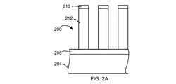
一実施形態のさらに具体的な例において、銅構造の下にバリア膜を備えたスタックが準備される(工程104)。図2Aは、銅構造212の下に蒸着されたバリア膜208の下に基板204を備えたスタック200を示す概略断面図である。この実施形態では、マスク216が、銅構造212の上にある。様々な実施形態において、マスク216は、1または複数の層によって形成されてもよいし、1または複数の層が、マスク216と銅構造212との間に配置されてもよい。さらに、1または複数の層が、バリア膜208と銅構造212との間、または、バリア膜208と基板204との間に配置されてもよい。
In a more specific example of an embodiment, a stack with a barrier film under a copper structure is provided (step 104). FIG. 2A is a schematic cross-sectional view showing a
この実施形態において、銅構造212は、純銅である。別の実施形態において、銅構造は、銅合金である。バリア膜208は、Ru、Co、Ta、Ti、TiN、Pt、W、または、TaNの内の少なくとも1つである。
In this embodiment, the
少なくとも1サイクルの循環処理が、バリア膜をエッチングするために提供される(工程108)。各サイクルは、バリア膜のウェット処理(工程112)およびバリア膜のドライスパッタリング(工程116)を含む。この実施形態において、ウェット処理は、バリア膜208のエッチングに効果的でありつつ、銅構造212をエッチングも劣化もさせない浴を含む。バリア膜208が、Co、Ta、Ti、TiN、または、TaNである場合、ウェット処理浴は、酸、緩衝剤、キレート剤であるか、または、アセチルアセトン、ヘキサフルオロアセチルアセトンを含む。酸浴は、酢酸またはギ酸の一方を含んでよく、緩衝剤は、酢酸またはギ酸と共に水酸化アンモニウム緩衝剤を含んでよく、キレート剤は、エチレンジアミン四酢酸、ニトリロ三酢酸、ピリジン−2,3−ジカルボン酸、メソ−2,3−ジメルカプトコハク酸、および、2,3−ジメルカプト−1−プロパノールを含んでよい。バリア膜208が、TaまたはTaNである場合、ウェット処理浴は、過酸化水素およびCu腐食防止剤(<10重量%の腐食防止剤)と混合された有機溶媒を含む。有機溶媒の例は、メタノール、エタノール、プロパノール、ジメチルスルホキシド(DMSO)、ジメチルホルムアミド(DMF)、アセトン、エチレングリコール、酢酸エチル、N−メチル−2−ピロリジノン(NMP)などである。好ましいCu腐食防止剤は、ベンゾトリアゾール(BTA)であり、腐食防止剤は、1)3−アミノ−1,2,4−トリアゾール(ATA)、テトラゾール(TTA)などのアゾール、2)N−フェニル−1,4−フェニレンジアミン(NPPD)などのアミン、3)システインおよびトリプトファンなどのアミノ酸、4)ベンゼンチオールおよび置換ベンゼンチオールなどのチオール基クーポンであってもよい。具体的なレシピは、31重量%のH2O2と、40重量%DMSO、0.4重量%BTAの半水溶液との1:1体積混合物であってよい。10nmのTaN膜が、15分間60℃のこの混合物に暴露されることによって除去されうる。
At least one cycle of cycling treatment is provided (step 108) to etch the barrier film. Each cycle includes wet processing of the barrier film (step 112) and dry sputtering of the barrier film (step 116). In this embodiment, the wet process includes a bath that is effective in etching the
この実施形態において、バリア膜のドライスパッタリング(工程116)は、腐食を起こさないCuバリア後ドライエッチングを提供し、これは、H2などのハロゲン捕捉種と共に、低濃度のハロゲン化学物質(BCl3、HBr、CF4、NF3、Cl2、HCl、HI、CHF3を含むが、これらに限定されない)を用いることによって達成される。H2流量とハロゲン流量との比を調整することにより、Cu腐食を避けつつ、バリア層を化学的にドライエッチングすることができる。ドライスパッタリングは、少量のハロゲン(この実施形態においては、20sccm以下のハロゲン)と、500sccmのH2とを含むスパッタリングガスを提供する。好ましくは、この実施形態は、H2とハロゲンとの流量比が5:1から200:1の範囲にあるスパッタリングガスを提供する。H2とハロゲンとの流量比は、5:1から50:1の間であることがより好ましい。プラズマ電源は、50W〜1000Wの励起電力、2mTorr〜50mTorrのチャンバ圧、20V〜600Vbのバイアス電圧、および、10℃〜120℃の静電チャックの温度を提供する。バイアスは、100V〜500Vの間であることがより好ましい。バイアスは、200V〜400Vの間であることが最も好ましい。 In this embodiment, dry sputtering of the barrier film (step 116) provides a non-corrosive Cu barrier post-dry etch that, along with halogen-scavenging species such as H 2 , has a low concentration of halogen chemicals (BCl 3 ). , HBr, CF 4 , NF 3 , Cl 2 , HCl, HI, CHF 3 ). By adjusting the ratio of the H 2 flow rate and the halogen flow rate, the barrier layer can be chemically dry-etched while avoiding Cu corrosion. Dry sputtering provides a sputtering gas containing a small amount of halogen (in this embodiment, 20 sccm or less halogen) and 500 sccm H 2 . Preferably, this embodiment provides a sputtering gas having a H 2 to halogen flow ratio in the range of 5:1 to 200:1. More preferably, the flow ratio of H 2 to halogen is between 5:1 and 50:1. The plasma power supply provides an excitation power of 50 W to 1000 W, a chamber pressure of 2 mTorr to 50 mTorr, a bias voltage of 20 V to 600 Vb, and a temperature of the electrostatic chuck of 10° C. to 120° C. More preferably, the bias is between 100V and 500V. Most preferably, the bias is between 200V and 400V.
このアプローチにおいて、バリア膜は、最初に膜をほぐした後に光ドライスパッタリングエッチングで異方性プロファイルを形成するために、ウェット化学処理される。図2Bは、ウェット処理(工程112)を施した後のスタック200の概略断面図である。バリア膜208の上面は、波打った線で示すように、ウェット処理によってほぐれている。図2Cは、ドライスパッタリング処理(工程116)を施した後のスタック200の概略断面図である。異方性プロファイル224が形成されている。図2Dは、ウェット処理(工程112)およびドライスパッタリング(工程116)の複数サイクル後のスタック200の概略断面図である。この例において、バリア膜208は、実質的にエッチングされているが、完全にはエッチングされていない。
In this approach, the barrier film is wet chemical treated to first form the film, followed by optical dry sputter etching to create an anisotropic profile. FIG. 2B is a schematic cross-sectional view of the
別の実施形態において、ウェットおよびドライサイクル(工程108)は、最初に光ドライスパッタリングで始まり、その後、損傷を受けた膜のウェット除去(工程112)に進んでよい。この手順は、所望の効果を達成するために複数回繰り返されてよく、化学的にバリア膜を除去してバリアをトレンチ内にスパッタリングしないように、Cu膜の完全性を守ることが重要である。 In another embodiment, the wet and dry cycle (step 108) may begin with optical dry sputtering first and then proceed to wet removal of the damaged film (step 112). This procedure may be repeated multiple times to achieve the desired effect, and it is important to protect the integrity of the Cu film so as to chemically remove the barrier film and not sputter the barrier into the trench. ..
炭素層が、銅構造上に蒸着される(工程120)。この保護層は、CH4、C2H2、CH3F、CH2F2、C4F8、および、C4F6などの化学物質(ただし、これらに限定されない)で形成されてよい。さらに、ウエハにわたる保護層の均一性を制御するために、H2およびN2などの他のガス(ただし、これらに限定されない)が、化学物質に追加されてもよい。図2Eは、炭素層232が蒸着された(工程120)後のスタック200の概略断面図である。
A carbon layer is deposited on the copper structure (step 120). The protective layer, CH 4, C 2 H 2 , CH 3 F, CH 2 F 2, C 4 F 8 and,, C 4 chemicals such as F 6 (however, but not limited to) may be formed by .. Additionally, other gases such as, but not limited to, H 2 and N 2 may be added to the chemistry to control the uniformity of the protective layer across the wafer. FIG. 2E is a schematic cross-sectional view of the
ハロゲンを用いたドライエッチング処理(工程124)が、バリア膜208のエッチングを完了させるために用いられる。この実施形態ではて、H2/ハロゲンを用いたエッチング処理が提供される。上述したようなH2/ハロゲンを用いたエッチング処理が用いられてよい。図2Fは、ハロゲンを用いたドライエッチング処理(工程124)後のスタック200の概略断面図である。この実施形態において、バリア膜208は完全にエッチングされており、その下にある基板204は部分的にエッチングされている。
A dry etching process using halogen (step 124) is used to complete the etching of the
この実施形態は、ドライまたはウェットのみでは所望の結果に達することができない場合に、ドライおよび化学作用を組み合わせた相互作用によってバリア膜の除去を強化する。各層におけるドライプラズマ処理と正しいウェット化学物質との相互作用は、プロファイル、側壁蒸着、および、Cu膜統合制御の最適な結果を得るために調整できる。 This embodiment enhances barrier film removal by a combined dry and chemical interaction when the desired results cannot be reached with dry or wet alone. The interaction of the dry plasma treatment with the correct wet chemistry in each layer can be tailored for optimal results of profile, sidewall deposition, and Cu film integration control.
この実施形態は、Cuエッチングバリア開口処理の課題を解決できる。この実施形態は、ウェット処理のみの場合に起きるテーパ状のプロファイルおよび短絡を引き起こす低トレンチ領域における金属蒸着を防ぐ。この実施形態は、ウェット処理のみの場合に起きるCu膜への攻撃およびバリア膜の等方性アンダーカットも防ぐ。この実施形態のドライおよびウェット除去の組み合わせは、トレンチ内に金属を蒸着することなしにバリア膜の異方性除去を達成するように、処理を調整することができる。プラズマ条件は、弱いウェット化学物質が、Cu膜に影響を与えずに、損傷した膜を除去できるように、損傷したバリア層を作るように調整されてよい。複数工程の繰り返しが、バリア材料の異なる膜スタックを除去するために適用されてよい。 This embodiment can solve the problem of Cu etching barrier opening processing. This embodiment prevents metal deposition in the low trench regions that causes tapered profiles and shorts that occur with wet processing only. This embodiment also prevents the attack on the Cu film and the isotropic undercut of the barrier film that occur when only the wet treatment is performed. The combined dry and wet removal of this embodiment can tune the process to achieve anisotropic removal of the barrier film without depositing metal in the trench. The plasma conditions may be adjusted to create a damaged barrier layer so that the weak wet chemistry can remove the damaged film without affecting the Cu film. Repeated multiple steps may be applied to remove film stacks with different barrier materials.
炭素膜蒸着は、マスクを侵食から、Cuラインを腐食から保護するのに役立つ。 Carbon film deposition helps protect the mask from erosion and the Cu lines from corrosion.
別の実施形態において、ドライスパッタリングは、ハロゲンを用いない処理である。別の実施形態においては、炭素蒸着処理は、SiNまたはAlOx(酸化アルミニウム)の蒸着に置き換えられてもよく、それにより、スペーサ蒸着を用いて、Cuラインおよびマスクを保護してよい。 In another embodiment, dry sputtering is a halogen-free process. In another embodiment, the carbon deposition process may be replaced with SiN or AlO x (aluminum oxide) deposition, whereby spacer deposition may be used to protect Cu lines and masks.
別の実施形態において、循環処理は、バリア膜208を完全に除去する。かかる実施形態では、炭素蒸着工程およびハロゲンエッチングは利用されない。一実施形態において、ウェットおよびドライ処理は、少なくとも3サイクル繰り返される。
In another embodiment, the cycling treatment completely removes the
図3は、本発明の別の実施形態のハイレベルフローチャートである。銅構造の下にバリア膜を備えたスタックが、プラズマ処理チャンバ内に配置される(工程304)。連続ガスおよびパルスガスが、プラズマ処理チャンバに流される(工程308)。連続ガスおよびパルスガスは、プラズマ化される(工程312)。プラズマを用いて、銅構造を損傷することなしにバリア膜を完全にエッチングする(工程316)。エッチングが完了すると、連続ガスおよびパルスガスの流れが停止される(工程320)。完全にエッチングされたスタックが、プラズマ処理チャンバから取り出される(工程324)。 FIG. 3 is a high level flowchart of another embodiment of the present invention. A stack with a barrier film under the copper structure is placed in the plasma processing chamber (step 304). Continuous gas and pulsed gas are flowed into the plasma processing chamber (step 308). The continuous gas and the pulsed gas are plasmatized (step 312). The plasma is used to completely etch the barrier film without damaging the copper structure (step 316). When the etching is complete, the flow of continuous gas and pulsed gas is stopped (step 320). The fully etched stack is removed from the plasma processing chamber (step 324).
図4は、本発明のこの実施形態で利用可能なプラズマ処理ツール401を含むプラズマ処理システム400の概略図である。プラズマ処理ツール401は、誘導結合プラズマエッチングツールであり、プラズマ処理チャンバ404を有するプラズマリアクタ402を備える。変成器結合電力(TCP)コントローラ450およびバイアス電力コントローラ455が、それぞれ、プラズマ処理チャンバ404内で生成されるプラズマ424に影響を与えるTCP電源451およびバイアス電源456を制御する。
FIG. 4 is a schematic diagram of a
TCPコントローラ450は、TCP整合回路網452によって調整された13.56MHzの高周波信号をプラズマ処理チャンバ404の近くに位置するTCPコイル453に供給するよう構成されたTCP電源451のための設定点を設定する。TCPコイル453をプラズマ処理チャンバ404から隔離しつつ、エネルギがTCPコイル453からプラズマ処理チャンバ404に伝わることを可能にするために、RF透過窓454が設けられる。
The
バイアス電力コントローラ455は、バイアス整合回路網457によって調整されたRF信号を、プラズマ処理チャンバ404内に配置されたチャック電極408に供給して、処理される基板204を受けるよう適合された電極408上で直流(DC)バイアスを生成するよう構成されたバイアス電源456のための設定点を設定する。
ガス供給機構すなわちガス供給源410が、ガスマニホルド417を介して取り付けられた1または複数のガス源を備えており、処理に必要となる適切な化学物質をプラズマ処理チャンバ404の内部に供給する。この例では、ガス源416は、少なくとも、H2ガス源481と、Heガス源482と、ハロゲンガス源483とを含む。ガス排出機構418が、圧力制御バルブ419と排出ポンプ420とを備えており、プラズマ処理チャンバ404内から粒子を除去して、プラズマ処理チャンバ404内を特定の圧力に維持する。
A gas supply mechanism or
温度コントローラ480が、冷却用電源484を制御することによって、チャック電極408内に設けられた冷却再循環システムの温度を制御する。プラズマ処理システムは、さらに、バイアス電力コントローラ455、TCPコントローラ450、温度コントローラ480、および、その他の制御システムを制御するために利用されてよい電子制御回路470を備える。プラズマ処理システム400は、さらに、終点検出器を備えてもよい。かかる誘導結合システムの一例は、カリフォルニア州フレモントのLamResearch社製のKiyoであり、シリコン、ポリシリコン、および、導電層をエッチングするために用いられる。本発明の別の実施形態において、容量結合システムが用いられてもよい。
図5は、本発明の実施形態で用いられる制御回路470を実装するのに適切なコンピュータシステム500を示すハイレベルブロック図である。コンピュータシステムは、集積回路、プリント基板、および、小型携帯デバイスから大型スーパコンピュータまで、多くの物理的形態を有してよい。コンピュータシステム500は、1または複数のプロセッサ502を備えており、さらに、電子表示デバイス504(画像、テキスト、および、その他のデータを表示するためのもの)と、メインメモリ506(例えば、ランダムアクセスメモリ(RAM))、ストレージデバイス508(例えば、ハードディスクドライブ)と、リムーバブルストレージデバイス510(例えば、光学ディスクドライブ)と、ユーザインターフェースデバイス512(例えば、キーボード、タッチスクリーン、キーパッド、マウス、または、その他のポインティングデバイスなど)と、通信インターフェース514(例えば、無線ネットワークインターフェース)と、を備えてもよい。通信インターフェース514は、リンクを介してコンピュータシステム500および外部デバイスの間でソフトウェアおよびデータを転送することを可能にする。システムは、さらに、上述のデバイス/モジュールが接続される通信インフラ516(例えば、通信バス、クロスオーバーバー、または、ネットワーク)を備えてもよい。
FIG. 5 is a high level block diagram illustrating a
通信インターフェース514を介して転送される情報は、電子信号、電磁信号、光信号、または、信号を搬送する通信リンクを介して通信インターフェース514によって受信できるその他の信号など、信号の形態であってよく、電線すなわちケーブル、光ファイバ、電話回線、携帯電話リンク、無線周波リンク、および/または、通信チャネルを用いて実施されてよい。かかる通信インターフェースを用いて、1または複数のプロセッサ502は、上述の方法のステップを実行する際に、ネットワークから情報を受信、または、ネットワークに情報を出力しうることが想定される。さらに、本発明の方法の実施形態は、プロセッサだけで実行されてもよいし、インターネットなどのネットワークを介して、処理の一部を分担する遠隔プロセッサと協働で実行されてもよい。
The information transferred via
「非一時的なコンピュータ読み取り可能媒体」という用語は、一般に、メインメモリ、二次メモリ、リムーバブルストレージ、および、ストレージデバイスなどのメディア(ハードディスク、フラッシュメモリ、ディスクドライブメモリ、CD−ROM、および、その他の形態の持続性メモリなど)を指すために用いられ、搬送波または信号など、一時的な対象を網羅すると解釈されるべきではない。コンピュータコードの例としては、コンパイラによって生成されたコードなどのマシンコードや、インタープリタを用いてコンピュータによって実行される高級言語コードを含むファイルが挙げられる。コンピュータ読み取り可能な媒体は、搬送波で具現化されたコンピュータデータ信号によって転送されると共にプロセッサが実行可能な一連の命令を表すコンピュータコードであってもよい。 The term "non-transitory computer-readable medium" generally refers to media such as main memory, secondary memory, removable storage, and storage devices (hard disks, flash memory, disk drive memory, CD-ROM, and others. Form of persistent memory, etc.) and should not be construed as encompassing transitory objects such as carriers or signals. Examples of computer code include machine code, such as code generated by a compiler, and files containing high level language code that is executed by a computer using an interpreter. The computer-readable medium may be computer code that represents a series of instructions that can be transferred by a computer data signal embodied in a carrier wave and executed by a processor.
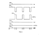
図6は、パルス処理の一例の概略図である。線604は、Heガスの流量が一定に保たれて連続ガスを提供することを示している(工程308)。この例において、Heガスの流量は、200〜1000sccmの間である。ライン608は、H2ガスのパルス流を示す。この例において、H2ガスの流量は、15〜30秒の期間に高流量であり、1〜5秒の期間に低流量である。この例において、H2の高流量は、100〜1000sccmの間である。この例において、H2の低流量は、0〜90sccmの間である。図に示すように、H2の流量は、タイムライン624で示されるように、t0〜t1、t2〜t3、t4〜t5、および、t6後の期間で、高流量である。線612は、ハロゲン含有ガスのパルス流を示す。この例において、ハロゲン含有ガスの流量は、1〜5秒の期間に高流量であり、15〜30秒の期間に低流量である。この例において、ハロゲン含有ガスの高流量は、500〜1000sccmの間である。この例において、ハロゲン含有ガスの低流量は、0〜100sccmの間である。図に示すように、ハロゲン含有ガスの流量は、t0〜t1、t2〜t3、t4〜t5、および、t6後の期間で、低流量である。ハロゲン含有ガスは、HBr、BCl3、Cl2、CF4、または、NF3の内の少なくとも1つを含むことが好ましい。H2ガスの高流量は、ハロゲン含有ガスの低流量の間に起きるので、それらのガスは、異なる位相でパルス化される。ハロゲン含有ガスの高流量も、H2ガスの低流量の間だけに起きるので、それらのガスは、完全に逆位相でパルス化される。
FIG. 6 is a schematic diagram of an example of pulse processing.
線616は、この例において、TCP電力が連続的かつ一定であることを示している。この例において、TCP電力は、200〜1000ワットの範囲である。別の例において、TCP電力は、パルス化されてもよい。線620は、この例において、バイアス電力が連続的かつ一定であることを示している。この例において、バイアス電力は、50〜400ボルトの範囲である。別の例において、バイアス電力は、パルス化されてもよい。TCP電力は、連続ガスおよびパルスガスをプラズマ化する(工程312)。
水素ガスをパルス化して、ほとんどの時間その流量を高く維持しつつ、ハロゲン含有ガスの流量をオフにすることにより、より高いバリア膜エッチング速度が得られることがわかった。ハロゲン含有ガスは、短期間だけ流される。水素は、Cu腐食効果を低減するために用いられる。オンおよびオフの期間は、バリア開口エッチング深さおよびCu腐食プロセスウィンドウのバランスを取るように調整されてよい。 It has been found that a higher barrier film etch rate can be obtained by pulsing the hydrogen gas and keeping the flow rate high for most of the time, while turning off the flow rate of the halogen containing gas. The halogen containing gas is flowed for a short period of time. Hydrogen is used to reduce the Cu corrosion effect. The on and off periods may be adjusted to balance the barrier opening etch depth and the Cu corrosion process window.
完全なドライ処理でバリア膜を除去する能力は、銅構造を腐食することも損傷することもなく、単一チャンバ処理を提供する。かかる処理は、より単純になる。別の実施形態では、容量結合電力(CCP)装置が用いられてもよい。遠隔プラズマ発生器など、他の装置が、プラズマを生成するために別の実施形態で用いられてもよい。別の実施形態において、連続ガスは、不活性搬送ガスである。連続ガスは、He、Ar、または、Neなどの希ガスであることが好ましい。H2高流量期間とハロゲン含有ガス高流量期間との比は、2:1から20:1の間(境界も含む)であることが好ましい。H2高流量期間とハロゲン含有ガス高流量期間との比は、3:1から15:1の間(境界も含む)であることがより好ましい。 The ability to remove the barrier film with a complete dry process provides a single chamber process without corroding or damaging the copper structure. Such a process becomes simpler. In another embodiment, a capacitively coupled power (CCP) device may be used. Other devices, such as remote plasma generators, may be used in alternative embodiments to generate the plasma. In another embodiment, the continuous gas is an inert carrier gas. The continuous gas is preferably a rare gas such as He, Ar, or Ne. The ratio of the H 2 high flow rate period and the halogen-containing gas high flow rate period is preferably between 2:1 and 20:1 (including the boundary). More preferably, the ratio of the H 2 high flow rate period and the halogen-containing gas high flow rate period is between 3:1 and 15:1 (including the boundary).
別の実施形態において、パルスガス処理は、少なくとも1回のウェットおよびドライサイクルの後に提供されてよい。 In another embodiment, pulsed gas treatment may be provided after at least one wet and dry cycle.
以上、いくつかの好ましい実施形態を参照しつつ本発明について説明したが、本発明の範囲内で、様々な代替物、置換物、および等価物が存在する。また、本発明の方法および装置を実施する他の態様が数多く存在することにも注意されたい。したがって、添付の特許請求の範囲は、本発明の真の趣旨および範囲内に含まれる代替物、置換物、および等価物の全てを網羅するものとして解釈される。例えば、本発明は、以下の適用例として実施可能である。
[適用例1]スタック内の銅構造の下のバリア膜を開口する方法であって、
ドライプラズマ処理チャンバ内に前記スタックを配置する工程と、
パルスガスを前記プラズマ処理チャンバ内に供給する工程であって、
パルスH 2 含有ガスを供給する工程と、
パルスハロゲン含有ガスを供給する工程とを含み、
前記パルスH 2 含有ガスおよび前記パルスハロゲン含有ガスは、異なる位相でパルス化され、前記パルスH 2 含有ガスは、H 2 高流量期間を有し、前記パルスハロゲン含有ガスは、ハロゲン含有ガス高流量期間を有し、前記H 2 高流量期間は、前記ハロゲン含有ガス高流量期間よりも長い工程と、
前記パルスガスをプラズマ化する工程と、
前記銅構造および前記バリア膜を前記プラズマに暴露させて、前記プラズマが前記バリア膜をエッチングする工程と
を備える方法。
[適用例2]適用例1に記載の方法であって、前記パルスガスをプラズマ化する工程は、
前記パルスガスを前記プラズマ処理チャンバ内に供給する工程中に、一定なRF電力信号を供給する工程と、
前記パルスガスを前記プラズマ処理チャンバ内に供給する工程中に、一定なバイアス電力を供給する工程と
を含む方法。
[適用例3]適用例2に記載の方法であって、さらに、前記パルスガスを前記プラズマ処理チャンバ内に供給する工程中に、一定流量の不活性搬送ガスを備える方法。
[適用例4]適用例3に記載の方法であって、前記ハロゲン含有ガスは、HBr、BCl 3 、Cl 2 、CF 4 、または、NF 3 の内の少なくとも1つを含む、方法。
[適用例5]適用例1に記載の方法であって、前記H 2 高流量期間と前記ハロゲン含有ガス高流量期間との比は、2:1から20:1の間(境界も含む)である方法。
[適用例6]適用例5に記載の方法であって、前記H 2 含有ガスおよびハロゲン含有ガスは、完全に逆位相でパルス化される方法。
[適用例7]適用例1に記載の方法であって、さらに、前記パルスガスを前記プラズマ処理チャンバ内に供給する工程中に、一定流量の不活性搬送ガスを備える方法。
[適用例8]適用例1に記載の方法であって、前記バリア膜は、Co、Ru、Ta、Ti、TaN、または、TiNの内の少なくとも1つを含む、方法。
[適用例9]適用例1に記載の方法であって、前記パルスガスをプラズマ化する工程は、
前記パルスガスを前記プラズマ処理チャンバ内に供給する工程中に、パルス化されたRF電力信号を供給する工程と、
前記パルスガスを前記プラズマ処理チャンバ内に供給する工程中に、パルス化されたバイアス電力を供給する工程と
を含む方法。
[適用例10]スタック内の銅構造の下のCo、Ru、Ta、Ti、TaN、または、TiNの内の少なくとも1つを含むバリア膜を開口する方法であって、
ドライプラズマ処理チャンバ内に前記スタックを配置する工程と、
一定流量の不活性搬送ガスを供給する工程と、
パルスガスを前記プラズマ処理チャンバ内に供給する工程であって、
パルスH 2 含有ガスを供給する工程と、
HBr、BCl 3 、Cl 2 、CF 4 、または、NF 3 の内の少なくとも1つを含むパルスハロゲン含有ガスを供給する工程とを含み、
前記パルスH 2 含有ガスおよび前記パルスハロゲン含有ガスは、異なる位相でパルス化され、前記パルスH 2 含有ガスは、H 2 高流量期間を有し、前記パルスハロゲン含有ガスは、ハロゲン含有ガス高流量期間を有し、前記H 2 高流量期間と前記ハロゲン含有ガス高流量期間との比は、2:1から20:1の間(境界も含む)である工程と、
前記一定流量のおよびガスパルスガスをプラズマ化する工程であって、
前記一定流量のガスおよびパルスガスを前記プラズマ処理チャンバ内に供給する工程中に、200から1000ワットの間のRF電力信号を供給する工程と、
前記一定流量のガスおよびパルスガスを前記プラズマ処理チャンバ内に供給する工程中に、50から500ボルトの間のバイアス電力を供給する工程とを含む工程と、
前記銅構造および前記バリア膜を前記プラズマに暴露させて、前記プラズマが前記バリア膜をエッチングする工程と
を備える方法。
[適用例11]銅構造の下のバリア膜を開口する方法であって、少なくとも1サイクルを含むウェットおよびドライ処理を提供する工程を備え、各サイクルは、
前記銅構造の下の前記バリア膜のウェット処理を提供する工程と、
前記銅構造の下の前記バリア膜のドライプラズマスパッタリングを提供する工程と
を連続的に含む方法。
[適用例12]適用例11に記載の方法であって、前記サイクルは、少なくとも3回繰り返される方法。
[適用例13]適用例12に記載の方法であって、ウェット処理を提供する工程は、酸、緩衝剤、または、キレート剤の浴、もしくは、アセチルアセトン、ヘキサフルオロアセチルアセトン、または、過酸化水素の内の少なくとも1つを含む浴を供給する方法。
[適用例14]適用例13に記載の方法であって、前記バリア膜は、Co、Ru、Ta、Ti、TaN、または、TiNの内の少なくとも1つを含む、方法。
[適用例15]適用例14に記載の方法であって、さらに、前記ウェットおよびドライ処理を提供する工程の後に、ドライハロゲン含有エッチングを提供する工程を備える方法。
[適用例16]適用例15に記載の方法であって、さらに、
前記ウェットおよびドライ処理を提供する工程の後かつ残りのバリア膜の前記ドライハロゲン含有エッチングの前に、前記銅構造に対して炭素、SiN、または、アルミニウムの蒸着を提供する工程を備える方法。
[適用例17]適用例16に記載の方法であって、前記ハロゲン含有エッチングを提供する工程は、
H 2 およびハロゲンを含むエッチングガスを供給する工程と、
前記エッチングガスをプラズマ化する工程と
を含む方法。
[適用例18]適用例17に記載の方法であって、前記ドライプラズマスパッタリングは、ハロゲンを用いない方法。
[適用例19]適用例17に記載の方法であって、前記ドライプラズマスパッタリングは、Cu腐食を引き起こさないような低いハロゲン含有量を有する方法。
[適用例20]適用例15に記載の方法であって、前記ドライハロゲン含有エッチングは、
連続的な不活性ガスを供給する工程と、
パルスH 2 ガスを供給する工程と、
前記パルスH 2 ガスと異なる位相で、パルスハロゲン含有ガスを供給する工程と、
残りのバリア膜をエッチングするプラズマを形成する工程と
を含む方法。
[適用例21]適用例20に記載の方法であって、さらに、50から400ボルトのバイアスを供給する工程を備え、前記プラズマを形成する工程は、200から1000ワットのRF電力を供給する工程を含む方法。
[適用例22]適用例11に記載の方法であって、さらに、前記ウェットおよびドライ処理を提供する工程の後に、ドライハロゲン含有エッチングを提供する工程を備える方法。
[適用例23]適用例22に記載の方法であって、さらに、
前記ウェットおよびドライ処理を提供する工程の後かつ残りのバリア膜の前記ドライハロゲン含有エッチングの前に、前記銅構造に対して炭素、SiN、または、アルミニウムの蒸着を提供する工程を備える方法。
[適用例24]適用例23に記載の方法であって、前記ハロゲン含有エッチングを提供する工程は、
H 2 およびハロゲンを含むエッチングガスを供給する工程と、
前記エッチングガスをプラズマ化する工程と
を含む方法。
[適用例25]適用例24に記載の方法であって、前記ドライプラズマスパッタリングは、ハロゲンを用いない方法。
[適用例26]適用例24に記載の方法であって、前記ドライプラズマスパッタリングは、Cu腐食を引き起こさないような低いハロゲン含有量を有する方法。
[適用例27]適用例22に記載の方法であって、前記ドライハロゲン含有エッチングは、
連続的な不活性ガスを供給する工程と、
パルスH 2 ガスを供給する工程と、
前記パルスH 2 ガスと異なる位相で、パルスハロゲン含有ガスを供給する工程と、
残りのバリア膜をエッチングするプラズマを形成する工程と
を含む方法。
[適用例28]適用例27に記載の方法であって、さらに、50から400ボルトのバイアスを供給する工程を備え、前記プラズマを形成する工程は、200から1000ワットのRF電力を供給する工程を含む方法。
[適用例29]銅構造の下のCo、Ru、Ta、Ti、TaN、または、TiNの内の少なくとも1つを含むバリア膜を開口する方法であって、
少なくとも3サイクルを含むウェットおよびドライ処理を提供する工程を備え、各サイクルは、
酸、緩衝剤、または、キレート剤の浴、もしくは、アセチルアセトン、ヘキサフルオロアセチルアセトン、または、過酸化水素の内の少なくとも1つを含む浴を供給することにより、前記銅構造の下の前記バリア膜のウェット処理を提供する工程と、
前記銅構造の下の前記バリア膜のドライプラズマスパッタリングを提供する工程と、
前記ウェットおよびドライ処理を提供する工程の後に、前記銅構造に対して炭素の蒸着を提供する工程と、
前記炭素の蒸着を供給する工程の後に、ドライハロゲン含有エッチングを提供する工程と
を連続的に含む方法。
Although the invention has been described with reference to some preferred embodiments, various alternatives, substitutions and equivalents exist within the scope of the invention. It should also be noted that there are numerous other ways of implementing the method and apparatus of the present invention. Therefore, the appended claims are to be construed to cover all alternatives, substitutions, and equivalents included within the true spirit and scope of the invention. For example, the present invention can be implemented as the following application examples.
Application Example 1 A method of opening a barrier film under a copper structure in a stack, comprising:
Placing the stack in a dry plasma processing chamber,
Supplying a pulsed gas into the plasma processing chamber,
Supplying a pulsed H 2 containing gas,
And a step of supplying a pulse halogen-containing gas,
The pulsed H 2 -containing gas and the pulsed halogen-containing gas are pulsed in different phases, the pulsed H 2 -containing gas has a high H 2 flow rate period, and the pulsed halogen-containing gas has a high halogen-containing gas flow rate. A period of time, and the H 2 high flow rate period is longer than the halogen-containing gas high flow rate period;
Converting the pulse gas into plasma,
Exposing the copper structure and the barrier film to the plasma, the plasma etching the barrier film;
A method comprising.
Application Example 2 The method according to Application Example 1, wherein the step of converting the pulse gas into plasma includes:
Supplying a constant RF power signal during the step of supplying the pulsed gas into the plasma processing chamber;
Supplying constant bias power during the step of supplying the pulse gas into the plasma processing chamber;
Including the method.
Application Example 3 The method according to Application Example 2, further comprising a constant flow rate of an inert carrier gas during the step of supplying the pulse gas into the plasma processing chamber.
Application Example 4 The method according to Application Example 3, wherein the halogen-containing gas contains at least one of HBr, BCl 3 , Cl 2 , CF 4 , or NF 3 .
Application Example 5 In the method described in Application Example 1, the ratio of the H 2 high flow rate period and the halogen-containing gas high flow rate period is between 2:1 and 20:1 (including the boundary). There is a way.
Application Example 6 The method according to Application Example 5, wherein the H 2 containing gas and the halogen containing gas are pulsed in completely opposite phases.
Application Example 7 The method according to Application Example 1, further comprising a constant flow rate of an inert carrier gas during the step of supplying the pulse gas into the plasma processing chamber.
Application Example 8 The method according to Application Example 1, wherein the barrier film contains at least one of Co, Ru, Ta, Ti, TaN, or TiN.
Application Example 9 In the method described in Application Example 1, the step of converting the pulse gas into plasma includes:
Providing a pulsed RF power signal during the step of supplying the pulsed gas into the plasma processing chamber;
Supplying pulsed bias power during the step of supplying the pulsed gas into the plasma processing chamber;
Including the method.
Application Example 10 A method of opening a barrier film containing at least one of Co, Ru, Ta, Ti, TaN, or TiN under a copper structure in a stack,
Placing the stack in a dry plasma processing chamber,
Supplying a constant flow rate of an inert carrier gas,
Supplying a pulsed gas into the plasma processing chamber,
Supplying a pulsed H 2 containing gas,
Supplying a pulsed halogen-containing gas comprising at least one of HBr, BCl 3 , Cl 2 , CF 4 , or NF 3 .
The pulsed H 2 -containing gas and the pulsed halogen-containing gas are pulsed in different phases, the pulsed H 2 -containing gas has a high H 2 flow rate period, and the pulsed halogen-containing gas has a high halogen-containing gas flow rate. A period, and the ratio of the H 2 high flow period and the halogen-containing gas high flow period is between 2:1 and 20:1 (including the boundary),
A step of plasmaizing the constant flow rate and gas pulse gas,
Providing an RF power signal between 200 and 1000 watts during the step of providing the constant flow of gas and the pulsed gas into the plasma processing chamber;
Supplying bias power between 50 and 500 volts during the step of supplying the constant flow rate of gas and the pulsed gas into the plasma processing chamber;
Exposing the copper structure and the barrier film to the plasma, the plasma etching the barrier film;
A method comprising.
Application Example 11 A method of opening a barrier film under a copper structure, comprising the steps of providing a wet and dry treatment including at least one cycle, each cycle comprising:
Providing a wet treatment of the barrier film under the copper structure,
Providing dry plasma sputtering of the barrier film below the copper structure;
The method including continuously.
Application Example 12 The method according to Application Example 11, wherein the cycle is repeated at least three times.
Application Example 13 The method according to Application Example 12, wherein the step of providing a wet treatment is performed by using a bath of an acid, a buffer or a chelating agent, or using acetylacetone, hexafluoroacetylacetone, or hydrogen peroxide. A method of providing a bath comprising at least one of:
Application Example 14 The method according to Application Example 13, wherein the barrier film contains at least one of Co, Ru, Ta, Ti, TaN, or TiN.
Application Example 15 The method according to Application Example 14, further comprising the step of providing a dry halogen-containing etching after the step of providing the wet and dry treatments.
Application Example 16 The method according to Application Example 15, further comprising:
A method comprising providing carbon, SiN, or aluminum vapor deposition to the copper structure after providing the wet and dry treatments and before the dry halogen containing etching of the remaining barrier film.
Application Example 17 The method according to Application Example 16, wherein the step of providing the halogen-containing etching comprises:
Supplying an etching gas containing H 2 and halogen,
A step of converting the etching gas into plasma
Including the method.
Application Example 18 The method according to Application Example 17, wherein the dry plasma sputtering does not use halogen.
Application Example 19 The method according to Application Example 17, wherein the dry plasma sputtering has a low halogen content that does not cause Cu corrosion.
Application Example 20 The method according to Application Example 15, wherein the dry halogen-containing etching is
Supplying a continuous inert gas,
Supplying pulsed H 2 gas,
Supplying a pulsed halogen-containing gas in a phase different from that of the pulsed H 2 gas;
A step of forming a plasma for etching the remaining barrier film,
Including the method.
Application Example 21 The method according to Application Example 20, further comprising the step of supplying a bias of 50 to 400 V, wherein the step of forming the plasma supplies RF power of 200 to 1000 watts. Including the method.
Application Example 22 The method according to Application Example 11, further comprising the step of providing a dry halogen-containing etching after the step of providing the wet and dry treatments.
Application Example 23 The method according to Application Example 22, further comprising:
A method comprising providing carbon, SiN, or aluminum vapor deposition to the copper structure after providing the wet and dry treatments and before the dry halogen containing etching of the remaining barrier film.
Application Example 24 The method according to Application Example 23, wherein the step of providing the halogen-containing etching comprises:
Supplying an etching gas containing H 2 and halogen,
A step of converting the etching gas into plasma
Including the method.
Application Example 25 The method according to Application Example 24, wherein the dry plasma sputtering does not use halogen.
Application Example 26 The method according to Application Example 24, wherein the dry plasma sputtering has a low halogen content that does not cause Cu corrosion.
Application Example 27 The method according to Application Example 22, wherein the dry halogen-containing etching is
Supplying a continuous inert gas,
Supplying pulsed H 2 gas,
Supplying a pulsed halogen-containing gas in a phase different from that of the pulsed H 2 gas;
A step of forming a plasma for etching the remaining barrier film,
Including the method.
Application Example 28 The method according to Application Example 27, further comprising the step of supplying a bias of 50 to 400 V, wherein the step of forming the plasma supplies RF power of 200 to 1000 watts. Including the method.
Application Example 29 A method of opening a barrier film containing at least one of Co, Ru, Ta, Ti, TaN, or TiN under a copper structure,
Providing a wet and dry treatment comprising at least 3 cycles, each cycle comprising:
By providing a bath of an acid, a buffer or a chelating agent or a bath containing at least one of acetylacetone, hexafluoroacetylacetone or hydrogen peroxide, the barrier film below the copper structure is provided. Providing a wet treatment,
Providing dry plasma sputtering of the barrier film under the copper structure,
Providing carbon deposition to the copper structure after providing the wet and dry treatments;
Providing a dry halogen-containing etch after the step of providing the carbon vapor deposition;
The method including continuously.
Claims (22)
ドライプラズマ処理チャンバ内に前記スタックを配置する工程と、
パルス化されたガスを前記ドライプラズマ処理チャンバ内に供給する工程であって、
H 2 高流量期間を有するようにパルス化されたH 2 含有ガスを供給する工程と、
ハロゲン含有ガス高流量期間を有するようにパルス化されたハロゲン含有ガスを供給する工程とを含み、
前記パルス化されたH2含有ガスおよび前記パルス化されたハロゲン含有ガスは、異なる位相でパルス化され、前記H2高流量期間は、前記ハロゲン含有ガス高流量期間よりも長い工程と、
前記パルス化されたガスをプラズマ化する工程と、
前記銅構造および前記バリア膜を前記プラズマに暴露させて、前記プラズマが前記バリア膜をエッチングする工程と
を備える方法。 A method of opening a barrier film under a copper structure in a stack, comprising:
Placing the stack in a dry plasma processing chamber,
Supplying a pulsed gas into the dry plasma processing chamber,
Supplying a H 2 containing gas pulsed to have a high H 2 flow rate period ;
Supplying a halogen-containing gas pulsed to have a high flow period of the halogen-containing gas .
The pulsed containing H 2 gas and the pulsed halogen-containing gas is pulsed at a different phase, before Symbol H 2 high flow period, and a long process than the halogen-containing gas and high flow period,
A step of plasma the pulsed gas,
Exposing the copper structure and the barrier film to the plasma, the plasma etching the barrier film.
前記パルス化されたガスを前記ドライプラズマ処理チャンバ内に供給する工程中に、一定なRF電力信号を供給する工程と、
前記パルス化されたガスを前記ドライプラズマ処理チャンバ内に供給する工程中に、一定なバイアス電力を供給する工程と
を含む方法。 The method of claim 1, the step of plasma the pulsed gas,
The pulsed gas during the process for supplying the dry plasma processing chamber, and supplying a constant RF power signal,
The pulsed gas during the process for supplying the dry plasma processing chamber, the method comprising the step of supplying a constant bias power.
前記パルス化されたガスを前記ドライプラズマ処理チャンバ内に供給する工程中に、パルス化されたRF電力信号を供給する工程と、
前記パルス化されたガスを前記ドライプラズマ処理チャンバ内に供給する工程中に、パルス化されたバイアス電力を供給する工程と
を含む方法。 The method of claim 1, the step of plasma the pulsed gas,
The pulsed gas during the process for supplying the dry plasma processing chamber, and supplying a pulsed RF power signal,
Method comprising the pulsed gas during the process for supplying the dry plasma processing chamber, and a step of supplying a bias power is pulsed.
ドライプラズマ処理チャンバ内に前記スタックを配置する工程と、
一定流量の不活性搬送ガスを供給する工程と、
パルス化されたガスを前記ドライプラズマ処理チャンバ内に供給する工程であって、
H 2 高流量期間を有するようにパルス化されたH 2 含有ガスを供給する工程と、
ハロゲン含有ガス高流量期間を有するようにパルス化されたハロゲン含有ガスであって、HBr、BCl3、Cl2、CF4、または、NF3の内の少なくとも1つを含むパルス化されたハロゲン含有ガスを供給する工程とを含み、
前記パルス化されたH2含有ガスおよび前記パルス化されたハロゲン含有ガスは、異なる位相でパルス化され、前記H2高流量期間と前記ハロゲン含有ガス高流量期間との比は、2:1から20:1の間(境界も含む)である工程と、
前記一定流量のおよび前記パルス化されたガスをプラズマ化する工程であって、
前記一定流量のガスおよび前記パルス化されたガスを前記ドライプラズマ処理チャンバ内に供給する工程中に、200から1000ワットの間のRF電力信号を供給する工程と、
前記一定流量のガスおよび前記パルス化されたガスを前記ドライプラズマ処理チャンバ内に供給する工程中に、50から500ボルトの間のバイアス電力を供給する工程とを含む工程と、
前記銅構造および前記バリア膜を前記プラズマに暴露させて、前記プラズマが前記バリア膜をエッチングする工程と
を備える方法。 A method of opening a barrier film comprising at least one of Co, Ru, Ta, Ti, TaN, or TiN under a copper structure in a stack comprising:
Placing the stack in a dry plasma processing chamber,
Supplying a constant flow rate of an inert carrier gas,
Supplying a pulsed gas into the dry plasma processing chamber,
Supplying a H 2 containing gas pulsed to have a high H 2 flow rate period ;
A pulsed halogen-containing gas to have a halogen-containing gas and high flow period, HBr, BCl 3, Cl 2 , CF 4, or a halogen-containing which is pulsed at least one of NF 3 And a step of supplying gas,
The pulsed containing H 2 gas and the pulsed halogen-containing gas is pulsed out of phase, the ratio between the before and Symbol H 2 high flow periods halogen-containing gas and high flow period, 2: 1 To 20:1 (including boundaries),
The constant flow of and the pulsed gas comprising the steps of: plasma,
The constant flow of gas and the pulsed gas during the process for supplying the dry plasma processing chamber, a process of supplying a RF power signal between 200 to 1000 watts,
During said constant flow rate of the gas and supplying the pulsed gas to the dry plasma processing chamber, a process including a step of supplying a bias power between 50 and 500 volts,
Exposing the copper structure and the barrier film to the plasma, the plasma etching the barrier film.
前記銅構造の下の前記バリア膜のウェット処理を提供する工程と、
前記銅構造の下の前記バリア膜のドライプラズマスパッタリングを提供する工程と
前記ウェット処理および前記ドライ処理を提供する工程の後に、ドライハロゲン含有エッチングを提供する工程と、
を連続的に含み、
前記ドライハロゲン含有エッチングは、
連続的な不活性ガスを供給する工程と、
パルス化されたH2ガスを供給する工程と、
前記パルス化されたH2ガスと異なる位相で、パルス化されたハロゲン含有ガスを供給する工程と、
残りのバリア膜をエッチングするプラズマを形成する工程と
を含み、
前記サイクルは、少なくとも3回繰り返され、
前記ウェット処理を提供する工程は、酸、緩衝剤、または、キレート剤の浴、もしくは、アセチルアセトン、ヘキサフルオロアセチルアセトン、または、過酸化水素の内の少なくとも1つを含む浴を供給し、
前記バリア膜は、Co、Ru、Ta、Ti、TaN、または、TiNの内の少なくとも1つを含む、方法。 A method of opening a barrier film under a copper structure comprising the steps of providing at least one cycle of wet and dry treatments, each cycle comprising:
Providing a wet treatment of the barrier film under the copper structure,
A step of providing dry plasma sputtering of the barrier film below the copper structure and a step of providing a dry halogen containing etch after the steps of providing the wet treatment and the dry treatment;
Including continuously,
The dry halogen-containing etching is
Supplying a continuous inert gas,
And supplying a pulsed H 2 gas,
In the pulsed H 2 gas and different phases, and supplying a pulsed halogen-containing gas,
Forming a plasma to etch the remaining barrier film,
The cycle is repeated at least 3 times,
The step of providing said wet treatment provides a bath of acid, buffer or chelating agent or a bath containing at least one of acetylacetone, hexafluoroacetylacetone or hydrogen peroxide,
The method, wherein the barrier film comprises at least one of Co, Ru, Ta, Ti, TaN, or TiN.
前記ウェット処理およびドライ処理を提供する工程の後かつ残りのバリア膜の前記ドライハロゲン含有エッチングの前に、前記銅構造に対して炭素、SiN、または、アルミニウムの蒸着を提供する工程を備える方法。 The method of claim 11, further comprising:
A method comprising providing carbon, SiN, or aluminum vapor deposition to the copper structure after providing the wet and dry treatments and before the dry halogen-containing etching of the remaining barrier film.
H2およびハロゲンを含むエッチングガスを供給する工程と、
前記エッチングガスをプラズマ化する工程と
を含む方法。 The method of claim 11, wherein the step of providing a dry halogen containing etch comprises:
Supplying an etching gas containing H 2 and halogen,
Converting the etching gas to plasma.
前記銅構造の下の前記バリア膜のウェット処理を提供する工程と、
前記銅構造の下の前記バリア膜のドライプラズマスパッタリングを提供する工程と
前記ウェット処理および前記ドライ処理を提供する工程の後に、ドライハロゲン含有エッチングを提供する工程と、
を連続的に含み、
前記ドライハロゲン含有エッチングは、
連続的な不活性ガスを供給する工程と、
パルス化されたH2ガスを供給する工程と、
前記パルス化されたH2ガスと異なる位相で、パルス化されたハロゲン含有ガスを供給する工程と、
残りのバリア膜をエッチングするプラズマを形成する工程と
を含む方法。 A method of opening a barrier film under a copper structure comprising providing a wet and dry process comprising at least one cycle, each cycle comprising:
Providing a wet treatment of the barrier film under the copper structure,
A step of providing dry plasma sputtering of the barrier film below the copper structure and a step of providing a dry halogen containing etch after the steps of providing the wet treatment and the dry treatment;
Including continuously,
The dry halogen-containing etching is
Supplying a continuous inert gas,
And supplying a pulsed H 2 gas,
In the pulsed H 2 gas and different phases, and supplying a pulsed halogen-containing gas,
Forming a plasma that etches the remaining barrier film.
前記ウェットおよびドライ処理を提供する工程の後かつ残りのバリア膜の前記ドライハロゲン含有エッチングの前に、前記銅構造に対して炭素、SiN、または、アルミニウムの蒸着を提供する工程を備える方法。 The method of claim 17, further comprising:
A method comprising providing carbon, SiN, or aluminum vapor deposition to the copper structure after providing the wet and dry treatment and before the dry halogen-containing etching of the remaining barrier film.
H2およびハロゲンを含むエッチングガスを供給する工程と、
前記エッチングガスをプラズマ化する工程と
を含む方法。 The method of claim 17, wherein the step of providing the dry halogen containing etch comprises:
Supplying an etching gas containing H 2 and halogen,
Converting the etching gas to plasma.
Applications Claiming Priority (4)
| Application Number | Priority Date | Filing Date | Title |
|---|---|---|---|
| US201462061774P | 2014-10-09 | 2014-10-09 | |
| US62/061,774 | 2014-10-09 | ||
| US14/579,822 US9570320B2 (en) | 2014-10-09 | 2014-12-22 | Method to etch copper barrier film |
| US14/579,822 | 2014-12-22 |
Publications (3)
| Publication Number | Publication Date |
|---|---|
| JP2016105461A JP2016105461A (en) | 2016-06-09 |
| JP2016105461A5 JP2016105461A5 (en) | 2018-11-15 |
| JP6749749B2 true JP6749749B2 (en) | 2020-09-02 |
Family
ID=55655956
Family Applications (1)
| Application Number | Title | Priority Date | Filing Date |
|---|---|---|---|
| JP2015199852A Active JP6749749B2 (en) | 2014-10-09 | 2015-10-08 | A new method for etching copper barrier films |
Country Status (4)
| Country | Link |
|---|---|
| US (1) | US9570320B2 (en) |
| JP (1) | JP6749749B2 (en) |
| KR (1) | KR102516921B1 (en) |
| TW (1) | TWI690992B (en) |
Families Citing this family (6)
| Publication number | Priority date | Publication date | Assignee | Title |
|---|---|---|---|---|
| US9899234B2 (en) * | 2014-06-30 | 2018-02-20 | Lam Research Corporation | Liner and barrier applications for subtractive metal integration |
| JP6761166B2 (en) * | 2015-07-23 | 2020-09-23 | セントラル硝子株式会社 | Wet etching method and etching solution |
| US11282714B2 (en) * | 2016-07-26 | 2022-03-22 | Central Glass Company, Limited | Etching method and etching device |
| KR102492733B1 (en) * | 2017-09-29 | 2023-01-27 | 삼성디스플레이 주식회사 | Copper plasma etching method and manufacturing method of display panel |
| US11322364B2 (en) * | 2020-04-01 | 2022-05-03 | Tokyo Electron Limited | Method of patterning a metal film with improved sidewall roughness |
| KR102574751B1 (en) * | 2021-12-07 | 2023-09-06 | 인하대학교 산학협력단 | Method for Dry Etching of Copper Thin Films |
Family Cites Families (12)
| Publication number | Priority date | Publication date | Assignee | Title |
|---|---|---|---|---|
| JPH08111420A (en) * | 1994-10-12 | 1996-04-30 | Fujitsu Ltd | Method and equipment for fabricating semiconductor device |
| US6143476A (en) * | 1997-12-12 | 2000-11-07 | Applied Materials Inc | Method for high temperature etching of patterned layers using an organic mask stack |
| US6177337B1 (en) * | 1998-01-06 | 2001-01-23 | International Business Machines Corporation | Method of reducing metal voids in semiconductor device interconnection |
| JP3490669B2 (en) * | 2000-07-18 | 2004-01-26 | 株式会社日立製作所 | Nonvolatile material etching method and apparatus |
| US6916746B1 (en) * | 2003-04-09 | 2005-07-12 | Lam Research Corporation | Method for plasma etching using periodic modulation of gas chemistry |
| JP5412517B2 (en) * | 2008-08-20 | 2014-02-12 | エーシーエム リサーチ (シャンハイ) インコーポレーテッド | Barrier layer removal method and apparatus |
| US8591661B2 (en) * | 2009-12-11 | 2013-11-26 | Novellus Systems, Inc. | Low damage photoresist strip method for low-K dielectrics |
| US8076778B2 (en) * | 2009-09-30 | 2011-12-13 | Macronix International Co., Ltd. | Method for preventing Al-Cu bottom damage using TiN liner |
| US20130323930A1 (en) * | 2012-05-29 | 2013-12-05 | Kaushik Chattopadhyay | Selective Capping of Metal Interconnect Lines during Air Gap Formation |
| JP2014086500A (en) * | 2012-10-22 | 2014-05-12 | Tokyo Electron Ltd | Method of etching copper layer, and mask |
| US8921234B2 (en) * | 2012-12-21 | 2014-12-30 | Applied Materials, Inc. | Selective titanium nitride etching |
| JP2014183184A (en) * | 2013-03-19 | 2014-09-29 | Tokyo Electron Ltd | Method for etching film containing cobalt and palladium |
-
2014
- 2014-12-22 US US14/579,822 patent/US9570320B2/en active Active
-
2015
- 2015-10-08 KR KR1020150141737A patent/KR102516921B1/en active IP Right Grant
- 2015-10-08 JP JP2015199852A patent/JP6749749B2/en active Active
- 2015-10-08 TW TW104133125A patent/TWI690992B/en active
Also Published As
| Publication number | Publication date |
|---|---|
| KR20160042396A (en) | 2016-04-19 |
| TW201628083A (en) | 2016-08-01 |
| JP2016105461A (en) | 2016-06-09 |
| US20160104630A1 (en) | 2016-04-14 |
| US9570320B2 (en) | 2017-02-14 |
| TWI690992B (en) | 2020-04-11 |
| KR102516921B1 (en) | 2023-03-31 |
Similar Documents
| Publication | Publication Date | Title |
|---|---|---|
| JP6749749B2 (en) | A new method for etching copper barrier films | |
| TWI650886B (en) | Method to etch non-volatile metal materials | |
| KR102127175B1 (en) | Method of etching copper layer and mask | |
| US8608973B1 (en) | Layer-layer etch of non volatile materials using plasma | |
| US20090184089A1 (en) | Fabrication of a silicon structure and deep silicon etch with profile control | |
| US8435419B2 (en) | Methods of processing substrates having metal materials | |
| JP6584022B2 (en) | Anisotropic etching of copper using passivation | |
| US10053773B2 (en) | Method of cleaning plasma processing apparatus | |
| CN104882360A (en) | Cleaning method for plasma processing apparatus | |
| US10192750B2 (en) | Plasma processing method | |
| KR101346897B1 (en) | Etching method and plasma processing system | |
| TW201735158A (en) | Hybrid stair-step etch | |
| TW201801184A (en) | Method for etching features in dielectric layers | |
| TWI703414B (en) | Etching method | |
| KR101540816B1 (en) | Plasma etching method, computer storage medium and plasma etching apparatus | |
| JP2016136617A (en) | Silicon etch and clean | |
| JP2016105461A5 (en) | ||
| US10242883B2 (en) | High aspect ratio etch of oxide metal oxide metal stack | |
| US20140179106A1 (en) | In-situ metal residue clean | |
| JP2017059750A (en) | Method for processing workpiece | |
| JP5164981B2 (en) | Method and apparatus for etching phase change alloy | |
| TWI806871B (en) | Porous low-k dielectric etch | |
| JP2016032117A (en) | Method of etching tungsten containing layer | |
| KR20220103781A (en) | processing chamber with multiple plasma units |
Legal Events
| Date | Code | Title | Description |
|---|---|---|---|
| A521 | Request for written amendment filed |
Free format text: JAPANESE INTERMEDIATE CODE: A523 Effective date: 20181005 |
|
| A621 | Written request for application examination |
Free format text: JAPANESE INTERMEDIATE CODE: A621 Effective date: 20181005 |
|
| A977 | Report on retrieval |
Free format text: JAPANESE INTERMEDIATE CODE: A971007 Effective date: 20190920 |
|
| A131 | Notification of reasons for refusal |
Free format text: JAPANESE INTERMEDIATE CODE: A131 Effective date: 20191029 |
|
| A521 | Request for written amendment filed |
Free format text: JAPANESE INTERMEDIATE CODE: A523 Effective date: 20200128 |
|
| TRDD | Decision of grant or rejection written | ||
| A01 | Written decision to grant a patent or to grant a registration (utility model) |
Free format text: JAPANESE INTERMEDIATE CODE: A01 Effective date: 20200714 |
|
| A61 | First payment of annual fees (during grant procedure) |
Free format text: JAPANESE INTERMEDIATE CODE: A61 Effective date: 20200812 |
|
| R150 | Certificate of patent or registration of utility model |
Ref document number: 6749749 Country of ref document: JP Free format text: JAPANESE INTERMEDIATE CODE: R150 |
|
| R250 | Receipt of annual fees |
Free format text: JAPANESE INTERMEDIATE CODE: R250 |