JP6742720B2 - Oxide layer etching method and etching apparatus - Google Patents
Oxide layer etching method and etching apparatus Download PDFInfo
- Publication number
- JP6742720B2 JP6742720B2 JP2015250922A JP2015250922A JP6742720B2 JP 6742720 B2 JP6742720 B2 JP 6742720B2 JP 2015250922 A JP2015250922 A JP 2015250922A JP 2015250922 A JP2015250922 A JP 2015250922A JP 6742720 B2 JP6742720 B2 JP 6742720B2
- Authority
- JP
- Japan
- Prior art keywords
- substrate
- oxide
- water
- active hydrogen
- processing chamber
- Prior art date
- Legal status (The legal status is an assumption and is not a legal conclusion. Google has not performed a legal analysis and makes no representation as to the accuracy of the status listed.)
- Active
Links
Images


Classifications
-
- H—ELECTRICITY
- H01—ELECTRIC ELEMENTS
- H01L—SEMICONDUCTOR DEVICES NOT COVERED BY CLASS H10
- H01L21/00—Processes or apparatus adapted for the manufacture or treatment of semiconductor or solid state devices or of parts thereof
- H01L21/02—Manufacture or treatment of semiconductor devices or of parts thereof
- H01L21/02104—Forming layers
- H01L21/02107—Forming insulating materials on a substrate
- H01L21/02296—Forming insulating materials on a substrate characterised by the treatment performed before or after the formation of the layer
- H01L21/02318—Forming insulating materials on a substrate characterised by the treatment performed before or after the formation of the layer post-treatment
- H01L21/02337—Forming insulating materials on a substrate characterised by the treatment performed before or after the formation of the layer post-treatment treatment by exposure to a gas or vapour
- H01L21/0234—Forming insulating materials on a substrate characterised by the treatment performed before or after the formation of the layer post-treatment treatment by exposure to a gas or vapour treatment by exposure to a plasma
-
- H—ELECTRICITY
- H01—ELECTRIC ELEMENTS
- H01L—SEMICONDUCTOR DEVICES NOT COVERED BY CLASS H10
- H01L21/00—Processes or apparatus adapted for the manufacture or treatment of semiconductor or solid state devices or of parts thereof
- H01L21/02—Manufacture or treatment of semiconductor devices or of parts thereof
- H01L21/04—Manufacture or treatment of semiconductor devices or of parts thereof the devices having at least one potential-jump barrier or surface barrier, e.g. PN junction, depletion layer or carrier concentration layer
- H01L21/18—Manufacture or treatment of semiconductor devices or of parts thereof the devices having at least one potential-jump barrier or surface barrier, e.g. PN junction, depletion layer or carrier concentration layer the devices having semiconductor bodies comprising elements of Group IV of the Periodic System or AIIIBV compounds with or without impurities, e.g. doping materials
- H01L21/30—Treatment of semiconductor bodies using processes or apparatus not provided for in groups H01L21/20 - H01L21/26
- H01L21/31—Treatment of semiconductor bodies using processes or apparatus not provided for in groups H01L21/20 - H01L21/26 to form insulating layers thereon, e.g. for masking or by using photolithographic techniques; After treatment of these layers; Selection of materials for these layers
- H01L21/3105—After-treatment
- H01L21/311—Etching the insulating layers by chemical or physical means
- H01L21/31105—Etching inorganic layers
- H01L21/31111—Etching inorganic layers by chemical means
- H01L21/31116—Etching inorganic layers by chemical means by dry-etching
-
- C—CHEMISTRY; METALLURGY
- C23—COATING METALLIC MATERIAL; COATING MATERIAL WITH METALLIC MATERIAL; CHEMICAL SURFACE TREATMENT; DIFFUSION TREATMENT OF METALLIC MATERIAL; COATING BY VACUUM EVAPORATION, BY SPUTTERING, BY ION IMPLANTATION OR BY CHEMICAL VAPOUR DEPOSITION, IN GENERAL; INHIBITING CORROSION OF METALLIC MATERIAL OR INCRUSTATION IN GENERAL
- C23C—COATING METALLIC MATERIAL; COATING MATERIAL WITH METALLIC MATERIAL; SURFACE TREATMENT OF METALLIC MATERIAL BY DIFFUSION INTO THE SURFACE, BY CHEMICAL CONVERSION OR SUBSTITUTION; COATING BY VACUUM EVAPORATION, BY SPUTTERING, BY ION IMPLANTATION OR BY CHEMICAL VAPOUR DEPOSITION, IN GENERAL
- C23C16/00—Chemical coating by decomposition of gaseous compounds, without leaving reaction products of surface material in the coating, i.e. chemical vapour deposition [CVD] processes
- C23C16/44—Chemical coating by decomposition of gaseous compounds, without leaving reaction products of surface material in the coating, i.e. chemical vapour deposition [CVD] processes characterised by the method of coating
- C23C16/458—Chemical coating by decomposition of gaseous compounds, without leaving reaction products of surface material in the coating, i.e. chemical vapour deposition [CVD] processes characterised by the method of coating characterised by the method used for supporting substrates in the reaction chamber
-
- C—CHEMISTRY; METALLURGY
- C23—COATING METALLIC MATERIAL; COATING MATERIAL WITH METALLIC MATERIAL; CHEMICAL SURFACE TREATMENT; DIFFUSION TREATMENT OF METALLIC MATERIAL; COATING BY VACUUM EVAPORATION, BY SPUTTERING, BY ION IMPLANTATION OR BY CHEMICAL VAPOUR DEPOSITION, IN GENERAL; INHIBITING CORROSION OF METALLIC MATERIAL OR INCRUSTATION IN GENERAL
- C23C—COATING METALLIC MATERIAL; COATING MATERIAL WITH METALLIC MATERIAL; SURFACE TREATMENT OF METALLIC MATERIAL BY DIFFUSION INTO THE SURFACE, BY CHEMICAL CONVERSION OR SUBSTITUTION; COATING BY VACUUM EVAPORATION, BY SPUTTERING, BY ION IMPLANTATION OR BY CHEMICAL VAPOUR DEPOSITION, IN GENERAL
- C23C16/00—Chemical coating by decomposition of gaseous compounds, without leaving reaction products of surface material in the coating, i.e. chemical vapour deposition [CVD] processes
- C23C16/44—Chemical coating by decomposition of gaseous compounds, without leaving reaction products of surface material in the coating, i.e. chemical vapour deposition [CVD] processes characterised by the method of coating
- C23C16/50—Chemical coating by decomposition of gaseous compounds, without leaving reaction products of surface material in the coating, i.e. chemical vapour deposition [CVD] processes characterised by the method of coating using electric discharges
-
- C—CHEMISTRY; METALLURGY
- C23—COATING METALLIC MATERIAL; COATING MATERIAL WITH METALLIC MATERIAL; CHEMICAL SURFACE TREATMENT; DIFFUSION TREATMENT OF METALLIC MATERIAL; COATING BY VACUUM EVAPORATION, BY SPUTTERING, BY ION IMPLANTATION OR BY CHEMICAL VAPOUR DEPOSITION, IN GENERAL; INHIBITING CORROSION OF METALLIC MATERIAL OR INCRUSTATION IN GENERAL
- C23C—COATING METALLIC MATERIAL; COATING MATERIAL WITH METALLIC MATERIAL; SURFACE TREATMENT OF METALLIC MATERIAL BY DIFFUSION INTO THE SURFACE, BY CHEMICAL CONVERSION OR SUBSTITUTION; COATING BY VACUUM EVAPORATION, BY SPUTTERING, BY ION IMPLANTATION OR BY CHEMICAL VAPOUR DEPOSITION, IN GENERAL
- C23C16/00—Chemical coating by decomposition of gaseous compounds, without leaving reaction products of surface material in the coating, i.e. chemical vapour deposition [CVD] processes
- C23C16/44—Chemical coating by decomposition of gaseous compounds, without leaving reaction products of surface material in the coating, i.e. chemical vapour deposition [CVD] processes characterised by the method of coating
- C23C16/52—Controlling or regulating the coating process
-
- H—ELECTRICITY
- H01—ELECTRIC ELEMENTS
- H01J—ELECTRIC DISCHARGE TUBES OR DISCHARGE LAMPS
- H01J37/00—Discharge tubes with provision for introducing objects or material to be exposed to the discharge, e.g. for the purpose of examination or processing thereof
- H01J37/32—Gas-filled discharge tubes
- H01J37/32009—Arrangements for generation of plasma specially adapted for examination or treatment of objects, e.g. plasma sources
-
- H—ELECTRICITY
- H01—ELECTRIC ELEMENTS
- H01J—ELECTRIC DISCHARGE TUBES OR DISCHARGE LAMPS
- H01J37/00—Discharge tubes with provision for introducing objects or material to be exposed to the discharge, e.g. for the purpose of examination or processing thereof
- H01J37/32—Gas-filled discharge tubes
- H01J37/32431—Constructional details of the reactor
- H01J37/3244—Gas supply means
- H01J37/32449—Gas control, e.g. control of the gas flow
-
- H—ELECTRICITY
- H01—ELECTRIC ELEMENTS
- H01J—ELECTRIC DISCHARGE TUBES OR DISCHARGE LAMPS
- H01J37/00—Discharge tubes with provision for introducing objects or material to be exposed to the discharge, e.g. for the purpose of examination or processing thereof
- H01J37/32—Gas-filled discharge tubes
- H01J37/32431—Constructional details of the reactor
- H01J37/32715—Workpiece holder
-
- H—ELECTRICITY
- H01—ELECTRIC ELEMENTS
- H01L—SEMICONDUCTOR DEVICES NOT COVERED BY CLASS H10
- H01L21/00—Processes or apparatus adapted for the manufacture or treatment of semiconductor or solid state devices or of parts thereof
- H01L21/02—Manufacture or treatment of semiconductor devices or of parts thereof
- H01L21/02104—Forming layers
- H01L21/02107—Forming insulating materials on a substrate
- H01L21/02296—Forming insulating materials on a substrate characterised by the treatment performed before or after the formation of the layer
- H01L21/02318—Forming insulating materials on a substrate characterised by the treatment performed before or after the formation of the layer post-treatment
- H01L21/02343—Forming insulating materials on a substrate characterised by the treatment performed before or after the formation of the layer post-treatment treatment by exposure to a liquid
-
- H—ELECTRICITY
- H01—ELECTRIC ELEMENTS
- H01L—SEMICONDUCTOR DEVICES NOT COVERED BY CLASS H10
- H01L21/00—Processes or apparatus adapted for the manufacture or treatment of semiconductor or solid state devices or of parts thereof
- H01L21/67—Apparatus specially adapted for handling semiconductor or electric solid state devices during manufacture or treatment thereof; Apparatus specially adapted for handling wafers during manufacture or treatment of semiconductor or electric solid state devices or components ; Apparatus not specifically provided for elsewhere
- H01L21/67005—Apparatus not specifically provided for elsewhere
- H01L21/67011—Apparatus for manufacture or treatment
- H01L21/67017—Apparatus for fluid treatment
- H01L21/67063—Apparatus for fluid treatment for etching
- H01L21/67075—Apparatus for fluid treatment for etching for wet etching
Description
本発明は、基板上の材料の層を除去する方法に関する。この方法は、特に、半導体基板上の二酸化シリコンおよび二酸化ゲルマニウムの原子スケールに忠実な正確な等方性除去に有効である。 The present invention relates to a method of removing a layer of material on a substrate. This method is particularly effective for the accurate isotropic removal of silicon dioxide and germanium dioxide on a semiconductor substrate, which is true to the atomic scale.
現代レベルの小型化における集積回路(IC)装置の製作には、原子スケールで動作できる技術が求められる。現在、あるIC装置部品は、材料のわずか数原子層に相当する数十オングストロームの大きさを有する。例えば、最新のICトランジスタにおけるゲート誘電体は、二酸化シリコンのわずか4原子層に相当するわずか12Åの厚さを有しうる。これらの部品の電子特性をそれらの大きさを変更することによって微調整することが望ましい場合が多く、これには材料の数原子層のみの堆積または除去が含まれるだろう。原子層堆積(ALD)および原子スケールのエピタキシャル成長技術が開発されてきたが、1つまたは複数の原子層の制御された除去方法は今もなお限られている。 Fabrication of integrated circuit (IC) devices in modern miniaturization requires technology capable of operating at the atomic scale. Currently, some IC device components have dimensions on the order of tens of angstroms, corresponding to only a few atomic layers of material. For example, the gate dielectric in a modern IC transistor may have a thickness of only 12Å, which corresponds to only 4 atomic layers of silicon dioxide. It is often desirable to fine-tune the electronic properties of these components by changing their size, which may include depositing or removing only a few atomic layers of material. Although atomic layer deposition (ALD) and atomic scale epitaxial growth techniques have been developed, methods of controlled removal of one or more atomic layers are still limited.
酸化シリコン、二酸化シリコンならびに、その炭素ドープ、ホウ素ドープ、およびリンドープ物は、IC装置で用いられる重要な誘電材料である。酸化シリコンは、バルク誘電体層では絶縁体として、トランジスタではゲート誘電体として、ダイナミック・ランダム・アクセス・メモリ(DRAM)などのメモリ装置では誘電体キャパシタとして機能する。酸化シリコンはまた、部分的に製作されたウエハが空気にさらされると、何らかの事情でシリコン層の上に形成されてしまう。自然酸化として知られるこの種類の酸化シリコンは、シリコン層の上に薄い膜を形成する。エッチングおよび/またはアッシング時に生成される酸化物残留とともに、自然酸化膜は、さらなる処理工程の問題となることが多い。自然酸化物および他の酸化物は、ビアが誘電材料で満たされた後にそれらがビアの全体的な電気抵抗を上げるため、シリコンが堆積したビアまたはコンタクトホールの底で形成される場合は、全く望まれない。 Silicon oxide, silicon dioxide and their carbon-doped, boron-doped, and phosphorus-doped compounds are important dielectric materials used in IC devices. Silicon oxide functions as an insulator in bulk dielectric layers, as a gate dielectric in transistors, and as a dielectric capacitor in memory devices such as dynamic random access memory (DRAM). Silicon oxide may also form on the silicon layer for some reason when the partially fabricated wafer is exposed to air. This type of silicon oxide, known as native oxidation, forms a thin film on the silicon layer. Native oxides, along with oxide residues generated during etching and/or ashing, are often a problem for further processing steps. Native oxides and other oxides do not exist at all if they are formed at the bottom of a silicon deposited via or contact hole because they increase the via's overall electrical resistance after the via is filled with a dielectric material. Not wanted
酸化シリコンの気相エッチングについて述べている文献は豊富にある。それらの処理の大半は、本質的にはプラズマ処理である。そこでは、反応ガスが処理チャンバ内に位置するプラズマ源に導入されて、酸化シリコンの表面と反応するイオン種および準安定種を生成し、揮発性のエッチング副生成物を形成する。それらの処理のほとんどでは、酸化シリコンのエッチング速度は、反応ガスの流量および組成物、プラズマ電力、基板温度、またはチャンバ圧力によって制御される。酸化シリコンのエッチング速度は時間の経過と共にほぼ一定であるため、これらの種類の処理は、基板上の全ての露出面上で均一および正確にエッチングされる層の量を正確に制御するのに余り適していない。これらの処理は、原子スケールでの材料の規定量の除去には適用されない。 There is a wealth of literature describing vapor phase etching of silicon oxide. Most of these processes are essentially plasma processes. There, a reactive gas is introduced into a plasma source located within the processing chamber to generate ionic and metastable species that react with the surface of the silicon oxide, forming volatile etching byproducts. In most of these processes, the silicon oxide etch rate is controlled by the reaction gas flow rate and composition, plasma power, substrate temperature, or chamber pressure. Since the etch rate of silicon oxide is nearly constant over time, these types of treatments are more than adequate to precisely control the amount of layers that are uniformly and accurately etched on all exposed surfaces on the substrate. Not suitable. These treatments do not apply to the removal of defined amounts of material on an atomic scale.
そのため、原子スケールの均一性および低欠陥率を有する、原子スケールでの物質規定量の除去のための確実な方法が必要である。 Therefore, there is a need for a reliable method for atomic scale material removal with atomic scale uniformity and low defectivity.
本明細書で述べる方法は、相互接続配線およびコンタクトの予備洗浄への適用、ゲート誘電体処理、メモリおよび論理装置の製造、または、1つもしくは複数の材料原子層の確実な除去が望ましい場合のその他の適用においてなど、集積回路を製造する過程で用いられてよい。酸化シリコンおよび酸化ゲルマニウムの混合物とともに、酸化シリコンおよび酸化ゲルマニウムの制御された量の等方性除去のための処理について述べる。 The methods described herein are applied to pre-clean interconnect wiring and contacts, gate dielectric processing, memory and logic device fabrication, or where reliable removal of one or more atomic layers of material is desired. It may be used in the process of manufacturing integrated circuits, such as in other applications. Treatments for controlled isotropic removal of silicon oxide and germanium oxide are described, as well as mixtures of silicon oxide and germanium oxide.
ある態様では、基板上の酸化物層を制御可能にエッチングする方法が提供される。そこでは、酸化物は、酸化シリコン、酸化ゲルマニウム、および酸化シリコンと酸化ゲルマニウムの組み合わせからなる群より選択される。「酸化物」には、アンドープ酸化物ならびに、ホウ素、炭素、またはリンがドープされている酸化シリコンおよび酸化ゲルマニウムなどのドープ酸化物の両方が含まれる。いくつかの実施形態では、エッチング方法は、露出したシリコンの存在下で、原子スケールに忠実にこれらの酸化物を制御可能および選択的に除去する。この方法は、(a)基板上の酸化物の表面を改質するために、処理チャンバに収容されている基板を活性水素含有種に接触させることであって、活性水素含有種は1つ以上のOH基を含む化合物、または水素プラズマで生成される水素含有種であることと、(b)酸化物の表面が改質された後に、非表面結合活性水素種を処理チャンバから除去することと、(c)(b)の後に、酸化物の改質された表面と反応する無水HFを処理チャンバに流すことであって、反応は水を生成することと、(d)(c)で生成された水を基板の表面から除去することと、を含む。いくつかの実施形態では、(a)における酸化物の表面の改質は、酸化物の表面に対する活性水素含有種の吸着である。いくつかの実施形態では、(除去された平均厚さを参照すると)動作(a)−(d)の単一サイクルで酸化物の約0.5〜10原子層を除去する。いくつかの実施形態では、そのサイクルは繰り返され、動作(a)−(d)はエッチング時に少なくとも2回実施される。 In one aspect, a method of controllably etching an oxide layer on a substrate is provided. There, the oxide is selected from the group consisting of silicon oxide, germanium oxide, and combinations of silicon oxide and germanium oxide. "Oxide" includes both undoped oxide and doped oxides such as silicon oxide and germanium oxide that are doped with boron, carbon, or phosphorus. In some embodiments, the etching method controllably and selectively removes these oxides in the presence of exposed silicon, fidelity to atomic scale. The method comprises (a) contacting a substrate contained in a processing chamber with an active hydrogen-containing species to modify the surface of an oxide on the substrate, wherein the active hydrogen-containing species is one or more. A compound containing an OH group, or a hydrogen-containing species produced by hydrogen plasma, and (b) removing non-surface bound active hydrogen species from the processing chamber after the surface of the oxide has been modified. , (C), (b), and then flowing anhydrous HF that reacts with the modified surface of the oxide into the processing chamber, the reaction producing water, and (d) producing in (c). Removing the deposited water from the surface of the substrate. In some embodiments, the surface modification of the oxide in (a) is the adsorption of active hydrogen-containing species on the surface of the oxide. In some embodiments, a single cycle of operations (a)-(d) (with reference to the average thickness removed) removes about 0.5-10 atomic layers of oxide. In some embodiments, the cycle is repeated and operations (a)-(d) are performed at least twice during etching.
いくつかの実施形態では、HF反応および基板の表面からの除水は、水が反応で生成されながら基板表面に吸着を継続させない温度および圧力下で同時に実施される。いくつかの実施形態では、動作(a)−(d)は約80℃以上の単一温度(例えば、約100℃以上)で実施される。 In some embodiments, the HF reaction and the removal of water from the surface of the substrate are carried out simultaneously at a temperature and pressure that does not allow the reaction to continue adsorbing to the surface of the substrate while water is produced. In some embodiments, operations (a)-(d) are performed at a single temperature of about 80° C. or higher (eg, about 100° C. or higher).
いくつかの実施形態では、活性水素含有種は、水が酸化物の表面から脱離する条件下で、酸化物の表面に吸着するまたは吸着を継続できるアルコールである。かかるアルコールの例は、水の蒸気圧より低い蒸気圧を有するアルコール、または水の蒸気圧よりそれほど高くない蒸気圧を有するアルコール(イソプロパノール、n−プロパノール、n−ブタノール、tert−ブタノール、エチレングリコール、プロピレングリコールなど)を含む。いくつかの実施形態では、動作(a)−(d)は、これらのアルコールが基板の表面から脱離しないようにする温度および圧力で実施される。 In some embodiments, the active hydrogen-containing species is an alcohol that can adsorb or continue to adsorb on the surface of the oxide under conditions where water desorbs from the surface of the oxide. Examples of such alcohols are alcohols having a lower vapor pressure than the vapor pressure of water or alcohol with a vapor pressure not much higher than the vapor pressure of water, (isopropanol, n- propanol, n- butanol, tert- butanol, ethylene glycol, Propylene glycol). In some embodiments, operations (a)-(d) are performed at temperatures and pressures that prevent these alcohols from desorbing from the surface of the substrate.
他の実施形態では、活性水素含有種は水素含有プラズマから形成され、水が酸化物の表面から脱離する条件下で基板を水素含有プラズマに接触させることによって、ヒドロキシ(OH)結合が酸化物の表面上に形成される。水素含有プラズマは、H2、アンモニア、ヒドラジン、水、フッ化水素、塩化水素、シラン、ジシラン、メタン、エタン、ブタン、およびこれらの組み合わせなどの水素含有ガスを含むガスから形成される。必要に応じて、水素含有ガスを含むガスに第2のガスが追加されてよい。かかる第2のガスの例は、酸素、一酸化二窒素、一酸化窒素、二酸化炭素、一酸化炭素、およびこれらの組み合わせを含む。必要に応じて、不活性ガス(例えば、ヘリウム、ネオン、アルゴン、またはこれらの組み合わせ)は水素含有ガスを含むガスに追加されてよい。 In another embodiment, the active hydrogen-containing species are formed from a hydrogen-containing plasma and the hydroxy (OH) bonds are oxidized by contacting the substrate with the hydrogen-containing plasma under conditions where water desorbs from the surface of the oxide. Formed on the surface of. The hydrogen-containing plasma is formed from a gas containing a hydrogen-containing gas such as H 2 , ammonia, hydrazine, water, hydrogen fluoride, hydrogen chloride, silane, disilane, methane, ethane, butane, and combinations thereof. If desired, a second gas may be added to the gas containing the hydrogen-containing gas. Examples of such second gases include oxygen, dinitrogen monoxide, nitric oxide, carbon dioxide, carbon monoxide, and combinations thereof. If desired, an inert gas (eg, helium, neon, argon, or combinations thereof) may be added to the gas containing hydrogen-containing gas.
いくつかの実施形態では、活性水素含有種は、プロパノール、ブタノール、ブトキシエタノール、ブタンジオール、エチレングリコール、メチレングリコール、プロピレングリコール、アミルアルコール、カルボン酸、およびこれらの組み合わせからなる群より選択される。ある特定の実施形態では、ブタノールが用いられる。アルコール(例えば、ブタノール)は基板上に吸着し、次にHF処理が除水と同時に実施される。 In some embodiments, the active hydrogen-containing species is selected from the group consisting of propanol, butanol, butoxyethanol, butanediol, ethylene glycol, methylene glycol, propylene glycol, amyl alcohol, carboxylic acids, and combinations thereof. In one particular embodiment, butanol is used. Alcohol (eg, butanol) is adsorbed on the substrate and then HF treatment is performed simultaneously with water removal.
いくつかの実施形態では、活性水素含有種は、メタノール、エタノール、プロパノール、ブタノール、ブトキシエタノール、エチレングリコール、メチレングリコール、プロピレングリコール、アミルアルコール、およびこれらの組み合わせからなる群より選択され、動作(a)−(d)は同じ温度で実施される。水が反応で生成されながら酸化物の表面から除去されるように、処理はこの実施形態で構成されることが好ましい。 In some embodiments, the active hydrogen-containing species is selected from the group consisting of methanol, ethanol, propanol, butanol, butoxyethanol, ethylene glycol, methylene glycol, propylene glycol, amyl alcohol, and combinations thereof, the action (a )-(D) are carried out at the same temperature. The treatment is preferably configured in this embodiment so that water is removed from the surface of the oxide as it is produced in the reaction.
いくつかの実施形態では、活性水素含有種は、動作(a)−(d)が同じ温度で実施され、水が反応で生成されながら酸化物の表面から除去される選択された条件における、水の蒸気圧より低いまたはそれほど高くない蒸気圧に特徴がある。温度は、反応が終了する前に、水が表面から脱離する一方で活性水素含有種は脱離しないように選択される。この実施形態では、除去される酸化物の量は、工程(a)における表面改質の量によって決定され、HFは過剰に導入されうる。 In some embodiments, the active hydrogen-containing species is water-removed under selected conditions in which operations (a)-(d) are carried out at the same temperature and water is removed from the surface of the oxide as the reaction is produced. It is characterized by vapor pressures below or not too high. The temperature is chosen such that water desorbs from the surface while active hydrogen containing species do not desorb before the reaction is complete. In this embodiment, the amount of oxide removed is determined by the amount of surface modification in step (a) and HF can be introduced in excess.
他の実施形態では、活性水素含有種は、メタノール、エタノール、水、水−アルコール共沸混合物、または水の蒸気圧より実質的に高い蒸気圧を有するOH含有種である。メタノール(または、上記の種のうちの1つ)は、(a)において酸化物の表面に吸着し、処理は、無水HFが(c)において制御された限定量で供給されるように構成される。この実施形態では、エッチングされる酸化物の量は、導入されるHFの量によって制御される。 In other embodiments, the active hydrogen containing species is methanol, ethanol, water, water-alcohol azeotrope, or OH containing species having a vapor pressure substantially higher than that of water. Methanol (or one of the above species) is adsorbed on the surface of the oxide in (a) and the treatment is arranged such that anhydrous HF is fed in a controlled and limited amount in (c). It In this embodiment, the amount of oxide etched is controlled by the amount of HF introduced.
いくつかの実施形態では、活性水素含有種は、(a)において第1の温度で酸化物の表面に吸着するメタノールまたはエタノールであり、(d)において基板の温度を第1の温度より高い第2の温度に上昇させることによって水が除去される。この方法のいくつかの実施形態では、無水HFの処理チャンバへの流れは水が除去される前に停止する。 In some embodiments, the active hydrogen-containing species is (a) methanol or ethanol that adsorbs to the surface of the oxide at a first temperature and (d) raises the temperature of the substrate above the first temperature. Water is removed by raising the temperature to 2. In some embodiments of this method, the flow of anhydrous HF to the processing chamber is stopped before water is removed.
いくつかの実施形態では、水は、(i)基板の温度を上げること、(ii)処理チャンバの圧力を下げること、(iii)基板をプラズマで処理すること、(iv)基板を電子ビームで処理すること、(iv)基板を電磁放射で照射すること、およびこれらの方法の組み合わせからなる群より選択した方法によって除去される。 In some embodiments, the water is (i) increasing the temperature of the substrate, (ii) lowering the pressure of the processing chamber, (iii) treating the substrate with a plasma, (iv) electron beaming the substrate. Removed by a method selected from the group consisting of treating, (iv) irradiating the substrate with electromagnetic radiation, and combinations of these methods.
本発明の別の態様では、基板上の酸化物層を制御可能にエッチングする方法は、無水HFを基板に吸着させることによって開始する。上述した方法と同様に、この方法は、酸化シリコン、酸化ゲルマニウム、およびこれら酸化物の組み合わせをエッチングするために用いられうる。いくつかの実施形態では、このエッチング方法は、露出したシリコンの存在下で制御可能にかつ選択的にこれらの酸化物を除去する。この方法は、(a)処理チャンバに収納されている基板を無水HFと接触させて、HFを基板上に吸着させることと、(b)非表面結合HFを処理チャンバから除去することと、(c)基板上に吸着したHFと反応させるために基板を活性水素含有種で処理することであって、活性水素含有種は1つ以上のOH基(例えば、アルコール)を含む化合物、または水素プラズマで生成される水素含有種であることと、(d)(c)において生成された水を基板の表面から除去すること、を含む。除水方法は、上述したものと同じであってよい。 In another aspect of the invention, the method of controllably etching an oxide layer on a substrate begins by adsorbing anhydrous HF to the substrate. Similar to the method described above, this method can be used to etch silicon oxide, germanium oxide, and combinations of these oxides. In some embodiments, the etching method controllably and selectively removes these oxides in the presence of exposed silicon. This method comprises: (a) contacting a substrate contained in a processing chamber with anhydrous HF to adsorb the HF onto the substrate, and (b) removing non-surface bound HF from the processing chamber. c) treating the substrate with an active hydrogen-containing species to react with HF adsorbed on the substrate, the active hydrogen-containing species being a compound containing one or more OH groups (eg alcohol), or hydrogen plasma. And (d) removing the water generated in (c) from the surface of the substrate. The water removal method may be the same as that described above.
いくつかの実施形態では、本明細書で述べる方法は、フォトリソグラフィックデバイス処理とあわせて用いられる。例えば、これらの方法は、フォトレジストを基板に塗布することと、フォトレジストを露光することと、フォトレジストをパターニングしてパターンを基板に搬送することと、フォトレジストを基板から選択的に除去すること、をさらに含んでよい。 In some embodiments, the methods described herein are used in conjunction with photolithographic device processing. For example, these methods include applying photoresist to a substrate, exposing the photoresist, patterning the photoresist and delivering a pattern to the substrate, and selectively removing the photoresist from the substrate. May further be included.
別の態様では、基板上の酸化物を制御可能にエッチングするためのエッチング装置について述べる。この装置は、処理ガス導入用の導入口を有する処理チャンバと、基板上の酸化物のエッチング時に基板を定位置に保持するように構成されている処理チャンバ内の基板支持体と、本明細書で述べるいずれかの方法の工程を実施するためのプログラム命令を備えるコントローラと、を備える。例えば、コントローラは、(a)基板上の酸化物の表面を改質するために処理チャンバに収納されている基板を活性水素含有種と接触させるプログラム命令であって、活性水素含有種は1つ以上のOH基を含む化合物、または水素含有プラズマで生成される水素含有種であり、酸化物は酸化シリコン、酸化ゲルマニウム(ドープ酸化物およびアンドープ酸化物を含む)、およびこれらの組み合わせからなる群より選択されるプログラム命令と、(b)酸化物の表面が改質された後に、非表面結合活性水素種を処理チャンバから除去するプログラム命令と、(c)(b)の後に、酸化物の改質された表面と反応する無水HFを処理チャンバに流すプログラム命令であって、反応は水を生成するプログラム命令と、(d)(c)で生成された水を基板の表面から除去するプログラム命令と、を備えてよい。いくつかの実施形態では、この装置は、基板における温度の急激かつ制御された変化を可能にする温度制御装置を備える。 In another aspect, an etching apparatus for controllably etching oxide on a substrate is described. The apparatus comprises a processing chamber having an inlet for introducing a processing gas, a substrate support within the processing chamber configured to hold the substrate in place during etching of oxides on the substrate, and And a controller with program instructions for performing the steps of any of the methods described in. For example, the controller is (a) a program instruction for contacting a substrate contained in the processing chamber with an active hydrogen-containing species to modify the surface of the oxide on the substrate, the active hydrogen-containing species being one. A compound containing an OH group as described above, or a hydrogen-containing species generated by hydrogen-containing plasma, wherein the oxide is silicon oxide, germanium oxide (including doped oxide and undoped oxide), and a combination thereof. A selected programming instruction and (b) a programming instruction for removing non-surface bound active hydrogen species from the processing chamber after the surface of the oxide has been modified; and (c) and (b) a modification of the oxide. Program instructions for flowing anhydrous HF that reacts with the conditioned surface into the processing chamber, the reaction being a program instruction for producing water and a program instruction for removing the water produced in (d) and (c) from the surface of the substrate. And may be provided. In some embodiments, the device comprises a temperature control device that allows for rapid and controlled changes in temperature at the substrate.
いくつかの実施形態では、上述の装置およびステッパを含むシステムが提供される。 In some embodiments, a system is provided that includes the apparatus and stepper described above.
さらに別の態様では、本明細書で述べる装置を制御するために非一時的なコンピュータ機械可読媒体が提供される。この機械可読媒体は、本明細書で述べるいくつかの方法を実施するためのコードを含む。例えば、その方法は、(a)基板上の酸化物の表面を改質するために処理チャンバに収納されている基板を活性水素含有種と接触させることであって、活性水素含有種は、1つ以上のOH基を含む化合物、または水素含有プラズマで生成される水素含有種であり、酸化物は酸化シリコン、酸化ゲルマニウム、およびこれらの組み合わせからなる群より選択されることと、(b)酸化物の表面が改質された後に、非表面結合活性水素種を処理チャンバから除去することと、(c)(b)の後に、酸化物の改質された表面と反応する無水HFを処理チャンバに流すことであって、反応は水を生成することと、(d)(c)で生成された水を基板の表面から除去すること、を含む。 In yet another aspect, a non-transitory computer machine-readable medium is provided for controlling the devices described herein. This machine-readable medium contains code for performing some of the methods described herein. For example, the method comprises: (a) contacting a substrate contained in a processing chamber with an active hydrogen-containing species to modify the surface of an oxide on the substrate, wherein the active hydrogen-containing species is 1 A compound containing one or more OH groups, or a hydrogen-containing species produced in a hydrogen-containing plasma, the oxide being selected from the group consisting of silicon oxide, germanium oxide, and combinations thereof; and (b) oxidation. Removing non-surface bound active hydrogen species from the processing chamber after the surface of the article has been modified, and (c)(b) providing anhydrous HF that reacts with the modified surface of the oxide to the processing chamber. The reaction includes producing water and removing the water produced in (d)(c) from the surface of the substrate.
本発明のこれらおよび他の特徴ならびに利点は、関連する図面を参照して以下に詳述される。 These and other features and advantages of the invention are detailed below with reference to the associated drawings.
本発明の態様は、半製品の集積回路など、酸化シリコンおよび酸化ゲルマニウム(ドープおよびアンドープ酸化シリコンおよび酸化ゲルマニウムを含む)の基板からの制御されたエッチングに関する。本発明の方法は、半導体基板の処理において特に用いられる一方で、他の適用にも採用されうる。記載される方法は、例えば約150Å以下の規模など、小規模で正確かつ等方的な材料の除去を達成する。実際に、それらの方法は、わずか数オングストロームまたは数十オングストロームの層の除去が望まれる場合に採用されうる。本明細書で述べる原子層エッチング方法は、エッチングサイクルを繰り返すことによってエッチングの深さを制御できるようにし、各サイクルは、わずか単原子層または準単原子層の材料を除去できる。これらの方法は、CVD型またはプラズマ型の装置(例えば、レジスト剥離チャンバ)で実施することができ、既存のウエハ製造処理に容易に統合できる。 Aspects of the invention relate to controlled etching of silicon oxide and germanium oxide (including doped and undoped silicon oxide and germanium oxide) from a substrate, such as a semi-finished integrated circuit. While the method of the present invention is particularly used in the processing of semiconductor substrates, it can also be employed in other applications. The method described achieves small scale, accurate and isotropic material removal, eg, on the order of about 150 liters or less. In fact, these methods can be employed when removal of layers of only a few angstroms or tens of angstroms is desired. The atomic layer etching method described herein allows the depth of etching to be controlled by repeating the etching cycle, each cycle capable of removing only a monoatomic layer or quasi-monoatomic layer material. These methods can be performed in CVD or plasma type equipment (eg, resist stripping chambers) and can be easily integrated into existing wafer fabrication processes.
これらの方法は、酸化シリコン、酸化ゲルマニウム、およびこれら酸化物の混合物をエッチングするために用いられうる。これらの酸化物は、(例えば、窒素、炭素、ホウ素、リンなどによって)ドープまたはアンドープされうる。本明細書で用いられる「酸化シリコン」は、様々な種類の酸化シリコン、ケイ酸塩、ならびに、テトラエチルオルトケイ酸塩(TEOS)、ホウケイ酸ガラス(BSG)、ホウリンケイ酸ガラス(BPSG)、高密度プラズマ(HDP)CVD酸化物、低大気圧(SA)CVD酸化物などのケイ酸系ガラスを含む。 These methods can be used to etch silicon oxide, germanium oxide, and mixtures of these oxides. These oxides can be doped or undoped (eg, with nitrogen, carbon, boron, phosphorus, etc.). As used herein, "silicon oxide" refers to various types of silicon oxide, silicates, as well as tetraethylorthosilicate (TEOS), borosilicate glass (BSG), borophosphosilicate glass (BPSG), high density plasma. Includes silica glass such as (HDP) CVD oxide, low atmospheric pressure (SA) CVD oxide.
原子層除去方法の適用は、予備洗浄動作、ゲート誘電体製造、フィン状酸化物凹部の処理、ならびに、ダイナミック・ランダム・アクセス・メモリ(DRAM)およびフラッシュメモリ装置などのメモリ装置のキャパシタ誘電体の処理を含むが、これらに限定されない。配線の原子層エッチング予備洗浄は、シリコン、活性シリコン、ポリシリコン、シリサイドコンタクトの酸化シリコンからの除去を含んでよい。シリサイドコンタクトは、一般に配線に用いられる、ニッケルやコバルトシリサイドなどの金属シリサイド、白金ニッケルシリサイドや他のシリサイド材料などの3元シリサイドを含む。活性シリコンコンタクトとは、一般に電気活性ドープシリコン材料で形成される電気活性コンタクトを指す。これらの方法は、10nm未満レベルでのデバイスの製作に特に適しており、FinFETや全周ゲート型(GAA)FETなどの二重ゲートトランジスタの製作に用いられうる。 The application of the atomic layer removal method applies to pre-cleaning operations, gate dielectric fabrication, fin-shaped oxide recess processing, and capacitor dielectric in memory devices such as dynamic random access memory (DRAM) and flash memory devices. Including but not limited to treatment. Atomic layer etch preclean of interconnects may include removal of silicon, active silicon, polysilicon, and silicide contacts from silicon oxide. Silicide contacts include metal suicides such as nickel and cobalt suicides, ternary suicides such as platinum nickel suicides and other suicide materials commonly used for interconnects. Active silicon contact generally refers to an electroactive contact formed of an electroactive doped silicon material. These methods are particularly suitable for making devices at sub-10 nm levels and can be used for making double gate transistors such as FinFETs and all-round gate (GAA) FETs.
記載の方法は、露出したシリコン、ゲルマニウム、またはシリコンゲルマニウムの存在下で、酸化シリコン、酸化ゲルマニウム、またはこれらの組み合わせの選択的なエッチングを可能にする。選択的なエッチングとは、エッチング速度率が、少なくとも5:1である選択性を指す。 The method described allows selective etching of silicon oxide, germanium oxide, or a combination thereof in the presence of exposed silicon, germanium, or silicon germanium. Selective etching refers to selectivity where the etch rate is at least 5:1.
記載の方法は、酸化シリコンと酸化ゲルマニウム両方のエッチングに用いられうるが、これらの方法は、例として酸化シリコンを用いて図示される。全ての記載される原理および実施形態の図は、酸化ゲルマニウムのエッチングにも適用されることを理解されたい。 Although the methods described can be used to etch both silicon oxide and germanium oxide, these methods are illustrated using silicon oxide as an example. It should be understood that all described principles and embodiments figures also apply to the etching of germanium oxide.
エッチングは、凹状部分(ビア、トレンチ、コンタクトホールなど)を有するまたは有しない基板上で実施することができ、酸化シリコンは、凹状部分のフィールド領域、側壁、および底部を含む基板上の任意の位置から除去されうる。エッチング反応の自己制限式の吸着メカニズムによって、酸化シリコンは等方的に除去されうる。つまり、実質的に同量の酸化物が凹状部分のフィールド領域、側壁、および底部から除去され、除去された酸化物の量は、凹状部分のアスペクト比とは実質的に無関係である。さらに、酸化物は高い均一性で除去されうる。つまり、実質的に同量の酸化物が半導体ウエハ基板の中心部およびエッジから除去されうる。NH4Fエッチング液に依存する方法と違い、本明細書で述べる方法は固体反応生成物を生成しないため、高アスペクト比の凹状部分内において低い欠陥率と優れた反復可能な等方性エッチングをもたらすことに注意することが重要である。 Etching can be performed on a substrate with or without recesses (vias, trenches, contact holes, etc.), and silicon oxide can be deposited anywhere on the substrate, including the recess's field regions, sidewalls, and bottom. Can be removed from. Silicon oxide can be isotropically removed by a self-limiting adsorption mechanism of the etching reaction. That is, substantially the same amount of oxide is removed from the field region, sidewalls, and bottom of the recess, and the amount of oxide removed is substantially independent of the aspect ratio of the recess. Furthermore, the oxide can be removed with high uniformity. That is, substantially the same amount of oxide can be removed from the center and edges of the semiconductor wafer substrate. Unlike methods that rely on NH 4 F etchants, the methods described herein do not produce solid reaction products, which results in low defect rates and excellent repeatable isotropic etching within high aspect ratio recesses. It is important to note that it brings.
HFを用いる酸化シリコンのエッチング機構
無水HFは、水またはアルコールなどの活性水素含有種がないときは二酸化シリコンをエッチングしない。無水HFが酸化シリコンの表面に接触するとき、式(1)に示すように、表面をエッチングすることなく表面に吸着する。
HF(ガス)←→HF(吸着後) …(1)
Silicon Oxide Etching Mechanism Using HF Anhydrous HF does not etch silicon dioxide in the absence of active hydrogen containing species such as water or alcohol. When anhydrous HF contacts the surface of silicon oxide, it adsorbs to the surface without etching the surface, as shown in equation (1).
HF (gas) ←→ HF (after adsorption) (1)
メタノールなどの活性水素含有種が表面に吸着するときは、吸着したHFと反応して、式(2)−(4)に示すように、活性エッチング種であるHF2 −イオンを形成する。このエッチング反応は、反応(4)に示すように、水および四フッ化ケイ素を生成する。
CH3OH(ガス)←→CH3OH(吸着後) …(2)
CH3OH(吸着後)+HF(吸着後)←→HF2 −(吸着後)+CH3OH2 +(吸着後)
…(3)
SiO 2 (s)+2HF2 −(吸着後)+2CH3OH2 +(吸着後)→SiF4(吸着後)+2H2O(吸着後)+2CH3OH …(4)
When an active hydrogen-containing species such as methanol is adsorbed on the surface, it reacts with the adsorbed HF to form HF 2 − ions, which are active etching species, as shown in formulas (2)-(4). This etching reaction produces water and silicon tetrafluoride, as shown in reaction (4).
CH 3 OH (gas) ←→ CH 3 OH (after adsorption) (2)
CH 3 OH (after adsorption) + HF (after adsorption) ←→ HF 2 − (after adsorption) + CH 3 OH 2 + (after adsorption)
…(3)
SiO 2 (s)+2HF 2 − (after adsorption)+2CH 3 OH 2 + (after adsorption)→SiF 4 (after adsorption)+2H 2 O (after adsorption)+2CH 3 OH (4)
四フッ化ケイ素は、基板の表面から容易に脱離する揮発性化合物であるが、吸着した水は、二酸化シリコンの制御されたエッチングを困難な作業にする多くの問題を生じさせる。第一に、基板の表面上の水の存在は、活性水素含有種(メタノールなど)が元々限られた量で供給されたとしても、HF2 −の形成およびエッチング反応の進行をもたらす。そのため、吸着した水の存在下では、反応は自己制限式ではなく、HFがある限り続行するだろう。さらに、基板上の水の存在は、式5に示すように、SiF4に酸化シリコン粒子を形成する。これらの粒子は、反応速度のより低い反復性とともに、エッチング時の不良および不均一性をもたらす。
3SiF4+2H2O→SiO2+2H2SiF6 …(5)
While silicon tetrafluoride is a volatile compound that readily desorbs from the surface of substrates, adsorbed water creates many problems that make controlled etching of silicon dioxide a difficult task. First, the presence of water on the surface of the substrate results in the formation of HF 2 − and the progress of the etching reaction, even if the active hydrogen containing species (such as methanol) were originally provided in limited amounts. Therefore, in the presence of adsorbed water, the reaction is not self-limiting and will continue as long as HF is present. Furthermore, the presence of water on the substrate forms silicon oxide particles in SiF 4 , as shown in equation 5. These particles lead to poor repeatability of reaction rates, as well as defects and non-uniformities during etching.
3SiF 4 +2H 2 O→SiO 2 +2H 2 SiF 6 (5)
活性水素含有種が、例えば加熱によって、水とともに基板の表面から脱離する場合、エッチング反応は停止することに注意することも重要である。そのため、エッチング反応で生成された水を脱離することと、少なくとも所望の量の酸化物がエッチングされるまで基板の表面上に活性水素含有種を維持することとの間に、微妙なバランスが求められるべきである。 It is also important to note that the etching reaction is stopped if the active hydrogen-containing species desorbs from the surface of the substrate with water, eg by heating. Thus, there is a delicate balance between desorbing the water produced in the etching reaction and maintaining the active hydrogen-containing species on the surface of the substrate until at least the desired amount of oxide is etched. Should be sought.
エッチング方法
図1は、本明細書で述べる実施形態に従う酸化シリコンおよび/または酸化ゲルマニウムのエッチング方法を示すプロセスフロー図である。図2A−2Dは、制御されたエッチング中の酸化シリコン含有基板の断面図の略図を示す。図1によると、処理は、101において、1つ以上のOH基を含む活性水素含有種に基板を接触させることによって開始する。活性水素含有種は、アルコール(「アルコール」にはグリコールが含まれる)、カルボン酸、水素含有プラズマから生成される水素含有種、および、いくつかの実施形態では水であってよい。アンモニアは、適した化合物の一覧から除外されることに注意されたい。適したアルコールの例は、メタノール、エタノール、n−プロパノール、イソプロパノール、n−ブタノール、tert−ブタノール、メチルブタノール、アミルアルコール、メチレングリコール、エチレングリコール、プロピレングリコールなどを含む。カルボン酸の例は、蟻酸、酢酸、プロピオン酸などを含む。様々な水素含有種の混合物も用いられうる。水素含有プラズマから生成される水素含有種の例は、水素含有イオンおよびラジカルを含む。活性水素含有種は、一般に、気体の状態で基板を収容する処理チャンバに導入され、N2、Ar、Ne、He、およびこれらの組み合わせなどのキャリアガスを伴ってよい。水素含有プラズマから生成される種は、基板を収容する処理チャンバでプラズマを形成することによって直接生成されうる、または、基板を収容しない処理チャンバで遠隔的に生成されて、基板を収容する処理チャンバに供給されうる。
Etching Method FIG. 1 is a process flow diagram illustrating a method for etching silicon oxide and/or germanium oxide according to embodiments described herein. 2A-2D show schematic cross-sectional views of silicon oxide containing substrates during controlled etching. According to FIG. 1, the process begins at 101 by contacting a substrate with an active hydrogen-containing species containing one or more OH groups. The active hydrogen-containing species can be alcohols (“alcohol” includes glycols), carboxylic acids, hydrogen-containing species produced from hydrogen-containing plasmas, and in some embodiments water. Note that ammonia is excluded from the list of suitable compounds. Examples of suitable alcohols include methanol, ethanol, n-propanol, isopropanol, n-butanol, tert-butanol, methylbutanol, amyl alcohol, methylene glycol, ethylene glycol, propylene glycol and the like. Examples of carboxylic acids include formic acid, acetic acid, propionic acid and the like. Mixtures of various hydrogen containing species may also be used. Examples of hydrogen-containing species produced from a hydrogen-containing plasma include hydrogen-containing ions and radicals. Active hydrogen-containing species is generally introduced into the process chamber housing the substrate in the form of gas, N 2, Ar, Ne, He, and may involve a carrier gas, such as combinations thereof. Species generated from a hydrogen-containing plasma can be generated directly by forming a plasma in a processing chamber containing a substrate, or can be generated remotely in a processing chamber containing no substrate to contain a substrate. Can be supplied to.
活性水素含有種は、例えば酸化シリコンに吸着することによって、および/または、基板の表面上のケイ素−酸素結合を修正することによって、基板上の酸化シリコン表面を改質する。例えば、アルコールまたはカルボン酸は、酸化シリコンの表面に化学吸着しうる。この工程は、基板の表面上にOH結合を形成することから、水酸化とも呼ばれる。この工程の温度および圧力などの処理条件は、化学吸着が水素含有種のバルク量の結露なしで起こるように選択される。いくつかの実施形態では、処理チャンバは、チャンバの壁に高級アルコールの結露を避けるために加熱されてよい。 The active hydrogen-containing species modify the silicon oxide surface on the substrate, for example by adsorbing on silicon oxide and/or by modifying the silicon-oxygen bonds on the surface of the substrate. For example, alcohols or carboxylic acids can chemisorb on the surface of silicon oxide. This process is also called hydroxylation because it forms OH bonds on the surface of the substrate. Processing conditions such as temperature and pressure for this step are selected so that chemisorption occurs without condensation of bulk amounts of hydrogen-containing species. In some embodiments, the processing chamber may be heated to avoid condensation of higher alcohols on the chamber walls.
水素含有種が吸着したあるいは酸化シリコンの表面を改質した後、動作103では非表面結合活性水素含有種が処理チャンバから除去される。これは、活性種(例えば、アルコールまたは酸)を除去するために、吸着した層を除去することなく、処理チャンバをパージおよび/または排気することで実行できる。水素プラズマで生成される種は、必要に応じてチャンバのパージングおよび/または排気と組み合わせて、単にプラズマを停止させて残留する種を減衰させることによって除去できる。パージングは、N2、Ar、Ne、およびこれらの組み合わせなどの任意の不活性ガスを用いて実行できる。
After adsorbing the hydrogen-containing species or modifying the surface of the silicon oxide, the non-surface bound active hydrogen-containing species are removed from the processing chamber at
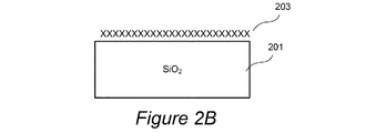
図2Aによると、酸化シリコン層を備える基板201が示されている。図2Bに示すように、水酸化および処理チャンバからの活性水素含有種のバルク量の除去の後は、基板201の上には表面層203のみが残る。表面層203は、例えばアルコールまたは他の水素含有種の化学吸着層であってよい。
According to FIG. 2A, a
次に、図1の工程105によると、基板は無水HFに接触する。無水HFは、活性水素含有種(例えば、アルコール、または水素プラズマで生成される種)の並流なしでチャンバに流入し、図2Cに示すように、酸化シリコンの改質層と反応することができる。いくつかの実施形態では、吸着した水素含有種によって反応が限定されるため、処理チャンバに導入されるHFの量は限定されない。他の実施形態では、目標の材料量だけをエッチングするように、HFは制御された限定量で供給されてよい。活性水素含有種の早期吸着が反応の停止を引き起こす可能性があるため、少なくともHF投与の前半部分では、活性水素含有種が基板の表面に結合したままになるように、処理条件は維持されるべきである。活性水素含有種の吸着は、所望のエッチング量が発生した後に開始されてよい。 Next, according to step 105 of FIG. 1, the substrate is contacted with anhydrous HF. Anhydrous HF may enter the chamber without co-current flow of active hydrogen-containing species (eg, alcohol, or hydrogen plasma generated species) and react with the modified layer of silicon oxide, as shown in FIG. 2C. it can. In some embodiments, the amount of HF introduced into the processing chamber is not limited because the reaction is limited by the adsorbed hydrogen-containing species. In other embodiments, HF may be provided in a controlled and limited amount so as to etch only the target amount of material. Since at least the first half of HF dosing, the process conditions are maintained such that the active hydrogen-containing species remain bound to the surface of the substrate, as premature adsorption of the active hydrogen-containing species can cause the reaction to stop. Should be. The adsorption of active hydrogen containing species may be initiated after the desired amount of etching has occurred.
動作107に示すように、エッチング反応で生成される水は、基板の表面から除去される。水を除去するために様々な方法が用いられうる。例えば、基板の表面からの水脱離は、十分に高い温度の基板を用いることによって達成されうる。温度は、水脱離を引き起こすように、または、水が反応の過程で生成されながら吸着しないように選択される。別の例では、除水は、十分に低い圧力を用いることによって達成され、適切な温度と組み合わせて、水が基板の表面上に吸着を継続しないようにする、または、水が生成されながら吸着しないように水を除去する。
As shown in
いくつかの実施形態では、除水は、水を除去するのに十分な温度に基板の温度を上昇させることによって達成される。いくつかの実施形態では、HF投与は、水を除去するのに十分な温度で実施される。いくつかの実施形態では、活性水素含有種を用いる処理およびHF投与を含む全てのエッチング処理は、水が生成されながら基板の表面から除去されるのに十分な温度で実施される。いくつかの実施形態では、除水は、水を除去するのに十分な圧力まで処理チャンバ内の圧力を下げることによって達成される。いくつかの実施形態では、HF投与は、水を除去するのに十分な圧力で実施される。いくつかの実施形態では、除水は、水を除去するための温度の上昇と圧力の低下の両方を含む。 In some embodiments, water removal is accomplished by raising the temperature of the substrate to a temperature sufficient to remove water. In some embodiments, HF administration is carried out at a temperature sufficient to remove water. In some embodiments, all etching processes, including treatment with active hydrogen-containing species and HF dosing, are performed at a temperature sufficient to remove water from the surface of the substrate as it is produced. In some embodiments, dewatering is accomplished by reducing the pressure in the processing chamber to a pressure sufficient to remove the water. In some embodiments, HF administration is performed at a pressure sufficient to remove water. In some embodiments, dewatering includes both increasing temperature and decreasing pressure to remove water.
いくつかの実施形態では、電磁照射(例えば、紫外線照射またはマイクロ波照射)、プラズマ処理(すなわち、電子、イオン、およびラジカル曝露)、および電子ビーム処理を用いて、水を表面から除去してよい。この照射、プラズマおよび電子ビーム処理のエネルギーは、基板の表面に損傷を及ぼさないように、またエッチングの等方性の妨げにならないように選択される。そのため、電子(プラズマまたは電子ビーム)処理のいくつかの実施形態では、約5〜10eVの間のエネルギーを有する電子など比較的低エネルギーの電子が用いられる。 In some embodiments, electromagnetic irradiation (eg, ultraviolet irradiation or microwave irradiation), plasma treatment (ie, electron, ion, and radical exposure), and electron beam treatment may be used to remove water from the surface. .. The energy of this irradiation, plasma and electron beam treatment is chosen so that it does not damage the surface of the substrate and does not interfere with the isotropy of the etching. As such, some embodiments of electron (plasma or electron beam) processing use relatively low energy electrons, such as electrons having energies between about 5-10 eV.
除水のタイミングは変えることが可能である。水の除去は、HF処理と同時に実施することができ、一部の時間帯にHF処理と重複してよい、またはHF処理の後に実施してよい。水の除去がHF処理の最初に実施される場合は、選択される除水方法は、酸化シリコンの表面をHFエッチングに対して完全には不活性化しないことに注意することが重要である。そのため、いくつかの実施形態では、水の除去は、酸化シリコンの表面からのアルコールまたはカルボン酸の脱離をもたらさないような条件下で実施される。エッチング反応時に生成される四フッ化ケイ素は、図2Dに示すように、一般に水とともに、または水が除去される前に基板の表面から除去される揮発性化合物である。酸化ゲルマニウムのエッチング時に形成される四フッ化ゲルマニウムも同様にして除去される。 The timing of removing water can be changed. The removal of water can be performed at the same time as the HF treatment, and may be overlapped with the HF treatment in some time periods or may be performed after the HF treatment. It is important to note that if water removal is performed at the beginning of the HF treatment, the water removal method chosen will not completely passivate the surface of the silicon oxide to HF etching. Therefore, in some embodiments, the removal of water is performed under conditions that do not result in the elimination of alcohol or carboxylic acid from the surface of the silicon oxide. Silicon tetrafluoride produced during the etching reaction is a volatile compound that is typically removed from the surface of the substrate either with water or before the water is removed, as shown in FIG. 2D. Germanium tetrafluoride formed during the etching of germanium oxide is also removed in the same manner.
図2Dに示す処理済みの基板では、制御された量の酸化シリコンが除去されているのがわかる。除去される酸化シリコンの量は、最初の水酸化工程における表面改質の量(例えば、吸着するアルコールの量)によって、および/または、基板上に投与されるHFの量によって決定される。重要なことには、活性水素含有種を過度の量にしないように、またHFを処理チャンバ内に同時に存在させないようにすることで制御が達成される。そのため、アルコールまたはカルボン酸が処理チャンバに投与されるときは、HFは処理チャンバに供給されない。同様に、HFが処理チャンバに供給されるときは、アルコールまたはカルボン酸は基板の表面上にのみ存在し、処理チャンバには供給されない。水の除去は、さらに、反応の原子スケールの制御に貢献する。一般に、1回のエッチングサイクルでは、約1〜5層の原子層など約0.5〜10層の酸化物原子層を除去する。ある実施形態では、約10Åの酸化シリコンが1回のエッチングサイクルで除去される。 It can be seen that the treated substrate shown in FIG. 2D has a controlled amount of silicon oxide removed. The amount of silicon oxide removed is determined by the amount of surface modification in the first hydroxylation step (eg, the amount of adsorbed alcohol) and/or the amount of HF dosed on the substrate. Importantly, control is achieved by not overdosing the active hydrogen containing species and by not allowing HF to be simultaneously present in the process chamber. Therefore, when alcohol or carboxylic acid is administered to the processing chamber, HF is not supplied to the processing chamber. Similarly, when HF is supplied to the processing chamber, the alcohol or carboxylic acid is only present on the surface of the substrate and not the processing chamber. The removal of water further contributes to the atomic scale control of the reaction. Generally, one etch cycle removes about 0.5-10 oxide atomic layers, such as about 1-5 atomic layers. In one embodiment, about 10ℓ of silicon oxide is removed in one etch cycle.
次に、動作109では、酸化シリコンの目標の厚さをエッチングするためにさらなるエッチングが必要であるかが決定される。最初のサイクルのエッチングで除去された量が十分であれば、エッチングは終了する。反応生成物またはHFがチャンバ内に残っているときは、処理チャンバはパージおよび/または排気される。必要に応じて、基板をアルコールに接触させて表面結合フッ化物を除去することによって、エッチング工程は111において終了する。
Next, in
動作109において、酸化シリコンの目標の厚さをエッチングするためにさらなるエッチングが必要であると決定された場合は、一連の動作が繰り返される。一般に、処理チャンバは、反応副生成物および余剰のHF(存在する場合)を除去するためにパージまたは排気され、基板の表面は再び活性水素含有種に接触する。次に、非表面結合活性水素含有種が除去され、次いでHF処理および除水が行われる。この処理は、必要な回数のサイクルで実施されうる。いくつかの実施形態では、約2〜10サイクルの間など、少なくとも2サイクルが実施される。繰り返しのサイクルで用いられる活性水素含有種は同じ、または異なるサイクルでは異なることに注意する。例えば、いくつかの実施形態では、最初のサイクルでは水が活性水素含有種として用いられ、その後のサイクルではアルコールが採用されてよい。
If in
いくつかの実施形態では、水がエッチング反応で生成されながら反応時に除去されることが好ましい。この実施形態は、図3に示すプロセス図によって示される。動作301では、基板は活性水素含有種(例えば、アルコール、カルボン酸、プラズマで生成される水素含有種)と接触し、酸化シリコンの表面を改質する。改質(例えば、アルコールの化学吸着)の後、非表面結合活性水素含有種は、例えば動作303におけるパージングまたは排気によって処理チャンバから除去され、次に動作305で基板に接触させるためにHFが供給され、水がエッチング反応で生成されながら除去されるために条件が維持される。例えば、HF処理時の基板の温度は、酸化シリコンの表面への水の吸着が不可能なように、または、水の急速な脱離をもたらすほどに十分高くてよい。他の実施形態では、圧力および温度は、水を表面から除去するのに十分なほど水脱離率が高くなるように維持される。さらに別の実施形態では、基板は、例えば紫外線放射、マイクロ波放射によって照射される、または、水を脱離するもしくは吸着することを防ぐのに十分なプラズマもしくは電子ビームによって処理されるが、基板はHFによって処理される。水がエッチング反応で生成されながらその場(in situ)で除去される利点は、水はエッチング反応にさらなる触媒作用を及ぼさないであろうことである。そのため、この実施形態では、追加されるHFの量に対してより少ない制御が求められる。いくつかの実施形態では、水が反応時に効率的かつ適時に除去される場合は、大量に過剰のHFを追加して、それでもなおエッチングされる酸化シリコンの量に対して原子スケールの制御を達成することも可能である。次に、反応が終了すると、処理チャンバは一般に、余剰のHF(存在する場合)および反応生成物を除去するためにパージまたは排気される。動作307においてさらなるエッチングが必要と判断された場合は、このサイクルが繰り返される。さらなるエッチングが必要ないときは、基板は、表面結合フッ素を除去するために必要に応じてアルコールによって処理されてよい。
In some embodiments, it is preferred that water is generated during the etching reaction and removed during the reaction. This embodiment is illustrated by the process diagram shown in FIG. In
図1および図3に示す処理は、基板の表面を整えるために様々な前処理および後処理によって修正されうる。いくつかの実施形態では、動作101の前に、基板はドライHFによって処理され、酸化シリコンの表面上のシラノール結合を除去する。処理チャンバは、次にパージまたは排気されてHFを除去する。他の前処理は、炭化水素またはハイドロフルオロカーボンなどの表面吸着汚染物質を除去するためのプラズマ処理またはウェット洗浄処理を含む。
The process shown in FIGS. 1 and 3 can be modified by various pre- and post-treatments to prepare the surface of the substrate. In some embodiments, prior to
図4は、図1および図3に示す処理のための試薬の投与を示すタイミング図である。第1期間P1では、活性水素含有種は、HFのない処理チャンバに供給される。いくつかの実施形態では、アルコールまたはカルボン酸は、P1時に反応チャンバに流入し、基板の表面上に化学吸着できる。他の実施形態では、水素含有プラズマから形成される活性水素含有種は、期間P1時に基板に接触する。次に、期間P2では、活性水素含有種およびHFのいずれもチャンバに入ることは許されない。この期間に、基板の表面に結合していない活性水素含有種は、処理チャンバから除去される。これは、例えば、不活性ガス(例えば、N2、Ar、He、Ne、およびその組み合わせ)による処理チャンバのパージングおよび/排気によって達成されうる。次に、期間P3では、無水HFは、活性水素含有種(アルコールなど)のない処理チャンバに流入し、基板の改質された表面と反応することができる。次に、期間P4では、HFおよび活性水素含有種のいずれも処理チャンバに流入せず、処理チャンバはパージまたは排気されて、処理チャンバ内の非表面結合HFおよび/または反応生成物を除去する。様々な実施形態において、除水は、HF投与と同時に(HF投与の全工程中に)、HF投与の後半に、HF投与の終了後に、およびこれらの組み合わせを用いて実施できる。記載した順序は、1サイクルのエッチングで終了し、基板の表面上の酸化シリコンの約0.5〜10層の原子層を制御可能にまた等方的にエッチングできる。次に、さらなるエッチングが必要な場合は、期間P5で活性水素含有種を投与することなどによって処理を繰り返す。いくつかの実施形態では、前のサイクルで生成された水の除去は、少なくとも一部は、処理期間の第1期間中または全期間中に、次のサイクルの活性水素種によって実施される。例えば、いくつかの実施形態では、第1のエッチングサイクルで生成された表面結合水は、期間P4で、または期間P5の前半に除去される。 FIG. 4 is a timing diagram showing administration of reagents for the processes shown in FIGS. 1 and 3. In the first period P1, the active hydrogen-containing species is supplied to the HF-free processing chamber. In some embodiments, the alcohol or carboxylic acid can enter the reaction chamber at P1 and chemisorb on the surface of the substrate. In another embodiment, the active hydrogen-containing species formed from the hydrogen-containing plasma contacts the substrate during period P1. Next, during the period P2, neither active hydrogen-containing species nor HF is allowed to enter the chamber. During this time, active hydrogen containing species that are not bound to the surface of the substrate are removed from the processing chamber. This can be accomplished, for example, by purging and/or evacuating the processing chamber with an inert gas (eg, N 2 , Ar, He, Ne, and combinations thereof). Then, in period P3, anhydrous HF can flow into the processing chamber free of active hydrogen-containing species (such as alcohol) and react with the modified surface of the substrate. Then, during period P4, neither HF nor active hydrogen containing species flow into the process chamber and the process chamber is purged or evacuated to remove non-surface bound HF and/or reaction products in the process chamber. In various embodiments, dewatering can be performed concurrently with HF administration (during all steps of HF administration), later in HF administration, after HF administration is complete, and with combinations thereof. The sequence described ends with one cycle of etching, and controllably and isotropically etches about 0.5-10 atomic layers of silicon oxide on the surface of the substrate. Then, if further etching is required, the process is repeated, such as by administering active hydrogen containing species in period P5. In some embodiments, the removal of water produced in the previous cycle is performed, at least in part, by the active hydrogen species of the next cycle, during the first or all of the treatment periods. For example, in some embodiments, the surface bound water produced in the first etch cycle is removed at time period P4 or in the first half of time period P5.
エッチングサイクルの各工程の温度および圧力などの処理条件は、活性水素含有種の性質、除水方法の種類、および除水のタイミングに依存し、本明細書で述べる指標の範囲内で変更できる。ほとんどの例では、温度は約20から約300℃の範囲、圧力は約100mTorrから約760torrの範囲である。以下に示す例は、本明細書中に記載されるエッチング方法のいくつかの異なる実施形態である。 The processing conditions such as the temperature and pressure of each step of the etching cycle depend on the nature of the active hydrogen-containing species, the type of water removal method, and the timing of water removal, and can be changed within the range of the index described herein. In most instances, the temperature will range from about 20 to about 300° C. and the pressure will range from about 100 mTorr to about 760 torr. The following examples are several different embodiments of the etching method described herein.
例1. この実施形態では、全てのエッチングサイクルは、水がエッチング反応で生成されながら吸着しないほどの十分な高温で実施される。いくつかの実施形態では、エッチング処理は、約80℃〜300℃の間など(例えば、100℃〜300℃の間)、約80℃以上の温度で実施される。この方法の利点は、全エッチングサイクル時の温度が実質的に一定に保たれうることである。さらに、水がエッチング反応時に生成されながら除去されるため、この実施形態ではHFを過剰に加えることができる。第1の水酸化工程の後は、酸化物の改質された表面上の活性水素含有種の量によって反応は制限されるからである。しかし、この実施形態は、過剰な量のHFを用いることに限定されず、いくつかの実施形態では、制御された限定量のHFが投与される。 Example 1. In this embodiment, all etching cycles are performed at a temperature high enough that water is generated in the etching reaction but does not adsorb. In some embodiments, the etching process is performed at a temperature of about 80° C. or higher, such as between about 80° C. and 300° C. (eg, between 100° C. and 300° C.). The advantage of this method is that the temperature during the entire etching cycle can be kept substantially constant. Furthermore, since water is removed as it is generated during the etching reaction, excess HF can be added in this embodiment. After the first hydroxylation step, the reaction is limited by the amount of active hydrogen-containing species on the modified surface of the oxide. However, this embodiment is not limited to using an excess amount of HF, and in some embodiments a controlled, limited amount of HF is administered.
この例のある特定の実施形態では、水の蒸気圧より低いまたは実質的に高くない(すなわち、200%より高くない)蒸気圧を有するアルコールまたはカルボン酸を処理で用いる。これらの化合物は、水が脱離している間に基板に吸着するまたは吸着を継続することができる。これらの化合物の例は、n−ブタノール、tert−ブタノール、エチレングリコール、プロピレングリコール、およびn−プロパノールを含む。第1期間P1では、かかる化合物またはかかる化合物の混合物は、基板の温度が水脱離点より高い間は、処理チャンバに流入して基板の表面上に吸着できる。次に、化合物の流入が止まり、期間P2では、実質的に温度を変えることなく処理チャンバはパージまたは排気される。次に、P3では、温度が十分に高いために、水が反応で生成されながら反応で生成した水を表面から除去する間に、無水HFは再び温度を変えることなく処理チャンバに流入し、酸化物の改質された表面と反応できる。次に、反応が終了すると、期間P4では、処理チャンバはパージおよび/または排気される。必要があれば、このサイクルは繰り返されうる。ある例では、n−ブタノールまたはtert−ブタノールが、約100℃の温度および約100Torrの圧力でN2とともに処理チャンバに導入され、基板上に化学吸着できる。次に、ブタノールの流れが止まり、処理チャンバはN2でパージされる。次に、温度の変化なく無水HFが処理チャンバに導入され、改質された酸化シリコンの表面層と反応できる。処理チャンバは次にN2でパージされ、処理は必要に応じて1〜3回繰り返される。 In certain embodiments of this example, an alcohol or carboxylic acid having a vapor pressure below or not substantially above water vapor pressure (ie, not above 200%) is used in the treatment. These compounds can adsorb or continue to adsorb to the substrate while water is desorbed. Examples of these compounds include n-butanol, tert-butanol, ethylene glycol, propylene glycol, and n-propanol. In the first period P1, such a compound or a mixture of such compounds can flow into the processing chamber and be adsorbed on the surface of the substrate while the temperature of the substrate is higher than the water desorption point. The compound inflow is then stopped and during period P2 the process chamber is purged or evacuated with substantially no change in temperature. Then, at P3, the temperature is sufficiently high so that anhydrous HF flows into the process chamber again without changing the temperature while water is being produced in the reaction while removing the water produced in the reaction from the surface. It can react with the modified surface of the object. Next, when the reaction is completed, in the period P4, the processing chamber is purged and/or evacuated. This cycle can be repeated if necessary. In one example, n-butanol or tert-butanol can be introduced into the process chamber with N 2 at a temperature of about 100° C. and a pressure of about 100 Torr and chemisorbed on the substrate. Then the butanol flow is stopped and the process chamber is purged with N 2 . Anhydrous HF is then introduced into the processing chamber without any change in temperature and can react with the surface layer of the modified silicon oxide. Processing chamber is then purged with N 2, the process is repeated 1-3 times if necessary.
例1の別の特定の実施形態では、酸化物の表面は、水素含有プラズマから形成される水素含有種と接触することによって改質される。期間P1では、基板は直接プラズマ(基板を収納する同じ処理チャンバで生成されるプラズマ)、または、活性水素含有種を含む遠隔プラズマ(異なるチャンバで生成されるプラズマ)と接触し、基板上の酸化シリコンの表面上にOH結合を形成する。様々なプラズマが用いられうる。一般に、プラズマは、必要に応じて存在する第2のガス(例えば、酸素、一酸化二窒素、一酸化窒素、二酸化炭素、一酸化炭素、水蒸気、およびその組み合わせ)とともに、水素含有ガス(例えば、H2、アンモニア、ヒドラジン、水、フッ化水素、塩化水素、シラン、ジシラン、メタン、エタン、ブタン、およびその組み合わせ)を含むガスから生成される。このガスは、水素含有ガスに加えて、He、Ar、Ne、およびその組み合わせなどの不活性ガスも含んでよい。プラズマ処理後は、P2においてプラズマの生成またはプラズマ生成種のチャンバへの流入が停止し、プラズマ生成種はチャンバ内で急速に腐敗する。次に、無水HFは、酸化物の活性表面との反応時に水が生成されると、基板の表面から水を除去するのに十分な気温と圧力で処理チャンバに流入する。 In another particular embodiment of Example 1, the surface of the oxide is modified by contacting with hydrogen-containing species formed from a hydrogen-containing plasma. During time period P1, the substrate is in direct contact with plasma (produced in the same processing chamber housing the substrate) or remote plasma containing active hydrogen-containing species (produced in a different chamber), and the substrate is oxidized. OH bonds are formed on the surface of silicon. Various plasmas can be used. In general, the plasma may include a hydrogen-containing gas (eg, oxygen, dinitrogen monoxide, nitric oxide, carbon dioxide, carbon monoxide, water vapor, and combinations thereof) optionally present with a second gas (eg, H2, ammonia, hydrazine, water, hydrogen fluoride, hydrogen chloride, silane, disilane, methane, ethane, butane, and combinations thereof). In addition to the hydrogen containing gas, this gas may also include an inert gas such as He, Ar, Ne, and combinations thereof. After the plasma treatment, the generation of plasma or the inflow of plasma-generated species into the chamber is stopped at P2, and the plasma-generated species is rapidly decomposed in the chamber. The anhydrous HF then flows into the processing chamber at a temperature and pressure sufficient to remove water from the surface of the substrate as water is produced during the reaction of the oxide with the active surface.
例2. この実施形態では、水は、電磁波照射(例えば、紫外線照射)によって、プラズマ処理(例えば、プラズマで形成された電子、ラジカル、イオン)によって、または電子ビーム処理によって基板の表面から除去される。水は、反応で生成されながら基板表面から除去される。この実施形態の利点は、基板の放射線に依存しない加熱が必要ないことである。さらに、この実施形態では、酸化物の表面を改質できる活性水素含有種の選択が、例1よりも広範囲にわたる。例1と同様に、反応時に水が除去されるため、HFは過剰に流入でき、除去酸化物の量は第1の工程における改質された酸化物の量によって決定される。この実施形態では、活性水素含有種(水、アルコール、カルボン酸、または水素プラズマで生成される種)は、期間P1で基板と接触し、酸化物の表面を改質する。この工程での温度および圧力は、吸着または他の改質が起こりうるように選択される。この実施形態は除水のための加熱に依存しないため、より低いアルコール(メタノールおよびエタノールなど)が用いられ、比較的低温(約10℃〜80℃の間など)で吸着されうる。次に、期間P2では、処理チャンバはパージおよび/もしくは排気され、または、プラズマで生成された水素含有種を減衰可能にする。期間P3では、水がウエハから同時に除去されている間に、照射、プラズマ処理、または電子ビーム処理によって、無水HFが導入される。 Example 2. In this embodiment, water is removed from the surface of the substrate by electromagnetic wave irradiation (eg, UV irradiation), plasma treatment (eg, plasma-generated electrons, radicals, ions), or electron beam treatment. Water is removed from the substrate surface as it is produced in the reaction. The advantage of this embodiment is that no radiation independent heating of the substrate is required. Furthermore, in this embodiment, the selection of active hydrogen containing species capable of modifying the surface of the oxide is more extensive than in Example 1. As in Example 1, since water is removed during the reaction, HF can flow in in excess and the amount of oxide removed is determined by the amount of modified oxide in the first step. In this embodiment, active hydrogen-containing species (water, alcohol, carboxylic acid, or species generated by hydrogen plasma) contact the substrate for a period P1 to modify the surface of the oxide. The temperature and pressure in this step are chosen so that adsorption or other reforming can occur. Since this embodiment does not rely on heating to remove water, lower alcohols (such as methanol and ethanol) are used and can be adsorbed at relatively low temperatures (such as between about 10°C and 80°C). Then, in period P2, the process chamber is purged and/or evacuated or allowed to decay hydrogen-containing species produced in the plasma. In period P3, anhydrous HF is introduced by irradiation, plasma treatment, or electron beam treatment while water is simultaneously removed from the wafer.
例3. この実施形態では、水を脱離するのに十分な温度に上昇させることによって、および/または、基板表面から水を脱離する条件を達成するために減圧することによって、基板の表面から水を除去する。 Example 3. In this embodiment, water is removed from the surface of the substrate by raising the temperature to a temperature sufficient to desorb the water and/or depressurizing to achieve conditions that desorb the water from the substrate surface. Remove.
例えば、基板は、第1の温度で活性水素含有種によって処理されてよい。活性水素含有種による処理後のある時点で、温度は基板の表面から水を脱離するのに十分な第2の温度に上昇される。例えば、活性種が水素含有プラズマから生成される種の場合、または、活性種が水の蒸気圧より低いもしくはそれほど高くない蒸気圧を有するアルコールもしくはカルボン酸であって、第2の温度が基板の表面の脱水酸化を引き起こさない場合は、温度は、非表面結合活性水素種の除去中もしくはHF導入と同時に、活性水素含有種による処理の後すぐにでも上昇させてよい。メタノールなど、水よりも著しく高い蒸気圧のアルコールが用いられる場合は(そのために第2の温度でメタノールは脱離する)、HFが導入されて反応が始まるまで温度の上昇を遅らせる方がより有利である。例えば、温度はHF導入期間の後半で上昇させてよい。いくつかの実施形態では、HFの流れが停止した後に温度が上昇する。いくつかの実施形態では、期間P5の前半(例えば、エッチングの第2サイクルにおけるメタノール導入時)に温度が上昇する、または高温が維持される。次に、期間P5の残りで温度が下がる。 For example, the substrate may be treated with the active hydrogen-containing species at the first temperature. At some point after treatment with the active hydrogen-containing species, the temperature is raised to a second temperature sufficient to desorb water from the surface of the substrate. For example, if the active species is a species generated from a hydrogen-containing plasma, or if the active species is an alcohol or carboxylic acid having a vapor pressure below or not much higher than the vapor pressure of water and the second temperature is the substrate temperature. If it does not cause surface dehydroxylation, the temperature may be raised during the removal of non-surface bound active hydrogen species or at the same time as the introduction of HF, shortly after treatment with active hydrogen containing species. If alcohol with a vapor pressure significantly higher than water is used, such as methanol (which causes the elimination of methanol at the second temperature), it is more advantageous to delay the temperature rise until HF is introduced and the reaction begins. Is. For example, the temperature may be raised in the latter half of the HF introduction period. In some embodiments, the temperature increases after the HF flow has stopped. In some embodiments, the temperature is raised or maintained at an elevated temperature during the first half of period P5 (eg, during the introduction of methanol in the second cycle of etching). Next, the temperature falls in the remainder of the period P5.
ある例では、メタノールは、期間P1で処理チャンバに流入し、第1の温度(例えば、約30℃)で化学吸着できる。次に、処理チャンバは非表面結合メタノールを除去するために期間P2でパージされ、HFは期間P3で処理チャンバに流入する。この実施形態では、制御された限定量のHFを導入することが好ましい。HFの量は、所望の酸化シリコンの制御された薄い層(約0.5〜10原子層など)をエッチングするのに必要な量に限定される。反応はしばらく進行してよく、その後温度は水の脱離を引き起こす温度(約100℃など)まで上昇する。いくつかの実施形態では、HFが処理チャンバに流入しながら、温度は期間P2で上昇する。他の実施形態では、温度は、HFの流れが止まってから(例えば、期間P5の前半で)上昇する。 In one example, methanol can enter the processing chamber for a period P1 and chemisorb at a first temperature (eg, about 30° C.). The process chamber is then purged during period P2 to remove non-surface bound methanol and HF flows into the process chamber during period P3. In this embodiment, it is preferred to introduce a controlled and limited amount of HF. The amount of HF is limited to the amount required to etch the desired controlled thin layer of silicon oxide (such as about 0.5-10 atomic layers). The reaction may proceed for some time, after which the temperature rises to a temperature that causes the elimination of water (such as about 100° C.). In some embodiments, the temperature rises during period P2 as HF flows into the processing chamber. In another embodiment, the temperature rises after the HF flow has stopped (eg, in the first half of period P5).
例4. この実施形態では、基板の表面からの水の除去を促進するために、メタノールおよび/またはケトン(例えば、アセトン)が用いられる。この例では、処理においてあらゆる活性水素含有種が用いられうるが、水の除去はメタノールおよび/またはケトン(例えば、アセトン)の存在下で促進されるため、エッチングの順序は、水をそれらと同時に除去するように構成される。メタノールおよび/またはケトンは、除水の前またはその最中のあらゆる適した段階で導入されうる。例えば、ある特定の例では、基板の表面は活性水素含有種によって水酸化され、次に処理チャンバがパージまたは排気され、続いて制御された量のHFが導入される。HFの導入時または反応が終了した後に、メタノールおよび/またはケトンは処理チャンバに流入し、条件は除水用に調整される(例えば、温度の上昇および/または減圧)。いくつかの実施形態では、処理を通して温度に変化がなくてよく、水の脱離を引き起こさないように、しかし水/メタノール混合物および/または水/ケトン混合物の脱離を引き起こすように選択される。 Example 4. In this embodiment, methanol and/or ketones (eg, acetone) are used to facilitate removal of water from the surface of the substrate. In this example, any active hydrogen-containing species can be used in the process, but the removal of water is facilitated in the presence of methanol and/or ketones (eg, acetone), so the etching sequence is such that Configured to remove. Methanol and/or ketone can be introduced at any suitable stage prior to or during dewatering. For example, in one particular example, the surface of the substrate is hydroxylated with an active hydrogen-containing species, then the process chamber is purged or evacuated, followed by the introduction of a controlled amount of HF. During the introduction of HF or after the reaction is complete, the methanol and/or ketone flows into the process chamber and the conditions are adjusted for water removal (e.g. elevated temperature and/or reduced pressure). In some embodiments, there may be no change in temperature throughout the treatment and it is selected so as not to cause the elimination of water, but to cause the elimination of water/methanol and/or water/ketone mixtures.
例5(代替実施形態). 上述の実施形態では、処理が基板上の酸化シリコン表面の水酸化で開始したのに対し、代替の実施形態では、処理は基板の表面への無水HFの吸着で開始してよい。次に、HFが吸着した後に、非表面結合HFは(例えば、パージングおよび/または排気によって)処理チャンバから除去され、基板は活性水素含有種と接触する。本明細書で述べるあらゆる活性水素含有種が用いられてよい。吸着したHFは、活性水素含有種の存在下で酸化シリコン表面と反応し、エッチングされた材料の量は、基板上に吸着したHFの量によって制限されるだろう。水は、先の実施形態で述べたように処理チャンバから除去される。水は、エッチング反応時(活性水素含有種の導入時)に生成されながら、または反応が終了した後に除去されてよい。 Example 5 (alternative embodiment). In the embodiments described above, the treatment started with the hydroxylation of the silicon oxide surface on the substrate, while in alternative embodiments the treatment may start with the adsorption of anhydrous HF on the surface of the substrate. Then, after the HF has been adsorbed, the non-surface bound HF is removed from the processing chamber (eg, by purging and/or evacuation) and the substrate is contacted with the active hydrogen containing species. Any active hydrogen-containing species described herein may be used. The adsorbed HF will react with the silicon oxide surface in the presence of active hydrogen containing species and the amount of material etched will be limited by the amount of HF adsorbed on the substrate. Water is removed from the processing chamber as described in previous embodiments. Water may be removed during the etching reaction (when introducing the active hydrogen-containing species) or after the reaction is completed.
装置
本明細書で述べる方法は、気体試薬の連続的な供給のために構成されている供給ラインおよび制御機構を備える様々な装置で実施できる。適した処理チャンバの例は、プラズマエッチング、等方性エッチング、化学気相堆積処理チャンバ、およびレジスト剥離チャンバを含む。腐食性HFの使用からの損傷を防ぐため、この装置は、少なくともHFと直接接触する部分には耐HF材料を備えてよい。例えば、いくつかの実施形態では、処理チャンバは、Halar(登録商標)として知られるエチレンとクロロトリフルオロエチレンとの共重合体などの耐HFポリマが塗布されている。いくつかの実施形態では、チャンバは陽極酸化またはニッケルめっきされている。HFを供給する供給ラインは、いくつかの実施形態ではニッケル製である。
Devices The methods described herein can be practiced on a variety of devices with supply lines and control mechanisms configured for continuous supply of gaseous reagents. Examples of suitable processing chambers include plasma etching, isotropic etching, chemical vapor deposition processing chambers, and resist strip chambers. To prevent damage from the use of corrosive HF, the device may be provided with an HF resistant material at least in direct contact with HF. For example, in some embodiments, the processing chamber is coated with an HF resistant polymer, such as a copolymer of ethylene and chlorotrifluoroethylene known as Halar®. In some embodiments, the chamber is anodized or nickel plated. The supply line that supplies HF is made of nickel in some embodiments.
適した装置は、エッチング時に基板を定位置に保持する基板支持体を有する処理チャンバと、試薬導入用の導入口と、一般に処理チャンバを排気するポンプと接続する流出口と、記載する方法のいずれかの工程を実施するためのプログラム命令を有するコントローラとを備える。いくつかの実施形態では、この装置は、所望通りに基板を加熱もしくは冷却するように構成されている加熱器および/または冷却器を備える。加熱器および/または冷却器は、基板支持体に統合されてよい。いくつかの実施形態では、基板の加熱は、基板上に熱を放散する、基板の上方に位置するランプを用いて実施してよい。このランプは、加熱の主要な方法として、または基板保持体の加熱に加えて用いられてよい。いくつかの実施形態では、基板保持体はモータを備え、処理時に基板を回転するように構成されている。処理チャンバで直接プラズマが(水素含有プラズマからの活性水素含有種の生成用または除水時の基板処理用のいずれかで)用いられる実施形態では、この装置はRFまたはマイクロ波プラズマ発生装置を備える。遠隔プラズマが(水素含有プラズマからの活性水素含有種の生成用または除水時の基板処理用のいずれかで)用いられる実施形態では、この装置は、RFまたはマイクロ波プラズマ発生装置を用いて遠隔プラズマが生成される別のチャンバを備える。この遠隔プラズマチャンバは、供給導管を通じて基板を収納する処理チャンバに接続し、遠隔プラズマで生成される種を基板の表面に供給するように構成されている。基板の表面から水を除去するために紫外線照射および/またはマイクロ波照射などの電磁波放射が用いられる実施形態では、この装置は、紫外線ランプまたはマイクロ波発生装置などの電磁波放射源も備える。これらの発生源は、一般に、用いられている特定の種類の電磁波放射を送る窓によって基板から隔離される。例えば、処理チャンバの天井を、サファイヤ被覆石英またはバルク石英の窓など耐HFの紫外線通過用窓で置き換えて、窓の上方に位置する紫外線ランプからの紫外線放射の通過を可能にしてもよい。 Suitable apparatus includes any of the methods described, a processing chamber having a substrate support that holds the substrate in place during etching, an inlet for introducing a reagent, and an outlet that generally connects with a pump to evacuate the processing chamber. And a controller having program instructions for performing the steps. In some embodiments, the apparatus comprises a heater and/or cooler configured to heat or cool the substrate as desired. The heater and/or cooler may be integrated into the substrate support. In some embodiments, heating the substrate may be performed with a lamp located above the substrate that dissipates the heat on the substrate. The lamp may be used as the primary method of heating or in addition to heating the substrate holder. In some embodiments, the substrate holder comprises a motor and is configured to rotate the substrate during processing. In embodiments where plasma is used directly in the processing chamber (either for generation of active hydrogen-containing species from hydrogen-containing plasma or for substrate processing during dewatering), the apparatus comprises an RF or microwave plasma generator. .. In embodiments where a remote plasma is used (either for the production of active hydrogen containing species from a hydrogen containing plasma or for treating the substrate during dewatering), the device is remote using an RF or microwave plasma generator. It comprises a separate chamber in which plasma is generated. The remote plasma chamber is connected through a supply conduit to a processing chamber containing the substrate and is configured to supply remote plasma generated species to the surface of the substrate. In embodiments where electromagnetic radiation such as ultraviolet radiation and/or microwave radiation is used to remove water from the surface of the substrate, the apparatus also comprises an electromagnetic radiation source such as an ultraviolet lamp or a microwave generator. These sources are generally separated from the substrate by windows that carry the particular type of electromagnetic radiation used. For example, the ceiling of the processing chamber may be replaced with an HF-resistant UV-transparent window, such as a sapphire-coated quartz or bulk quartz window, to allow passage of UV radiation from a UV lamp located above the window.
本明細書に記載するエッチング方法を実施するのに適した処理チャンバの例の略図が図5に示されている。処理チャンバ500は、遮断弁または流量制御弁と結合する気体試薬導入用の導入口502を備える。供給ライン504は、試薬源506を導入口502に接続する。いくつかの実施形態では、供給ライン504は、複数の個別のライン(例えば、無水HFラインやアルコール供給ライン)を含んでよい。いくつかの実施形態では、供給ラインは加熱源と接続し、ライン内の試薬の凝結を防ぐために試薬の供給時に加熱される。試薬源は無水HF源を含み、アルコールまたはカルボン酸が用いられる場合は、アルコール源またはカルボン酸源を含む。試薬源はまた、処理チャンバをパージするための不活性ガス源、および、水素含有プラズマ形成のための水素含有ガス源も備えてよい。供給ラインを備える供給システムは、一般に、処理チャンバに流入する試薬量の正確な計測に用いられる1つ以上の流量計も備える。処理チャンバはまた、排出弁およびポンプ510と接続する排出口508も有する。余剰の試薬、反応生成物、およびパージ用ガスは、排出弁が開いているときは排出口を通ってチャンバから排出する。処理チャンバ内の圧力は、試薬の流量を制御することによって、また処理チャンバから余剰のガスを排出することによって、正確に制御できる。
A schematic diagram of an example of a processing chamber suitable for carrying out the etching methods described herein is shown in FIG. The
基板512は、基板を加熱するように構成されている熱電チャック514をさらに備える基板保持台座516の上に固定される。図示された実施形態では、処理チャンバの天井は、必要に応じて透明または半透明の窓518であり、基板を紫外線で照射し、基板の表面から水を除去するのに用いられる紫外線ランプ520から処理チャンバを隔離する。他の実施形態では、放射熱を放出できる赤外線ランプは、処理チャンバの天井の上方に位置し、基板の表面を加熱するのに用いられる。いくつかの実施形態では、この装置は、基板上方に紫外線ランプおよび赤外線ランプまたは他の熱源の両方を備えてよい。コントローラ522は、この装置に電気的に接続され、エッチング処理の全ての段階を制御するのに用いられる。コントローラ522は、プログラム命令または内蔵ロジックを含み、本明細書で述べる実施形態のいずれかに従ってエッチング方法を実施する。例えば、コントローラは、試薬供給のタイミング、エッチングサイクルの各段階での温度および圧力、基板照射に関連するパラメータを特定するコードを含んでよい。
The
いくつかの実施形態では、コントローラは、上述の例の一部でありうるシステムの一部である。かかるシステムは、処理ツール、チャンバ、処理用のプラットフォーム、および/または特定の処理部品(ウエハ台座、ガス流システムなど)を含む半導体処理装置を備えうる。これらのシステムは、半導体ウエハまたは基板の処理前、処理中、および処理後にそれらの動作を制御する電子部品と統合されてよい。電子部品は「コントローラ」と呼ばれ、システムの様々な構成部品または補助部品を制御してよい。コントローラは、処理要件および/またはシステムの種類によって、処理ガス供給、温度設定(例えば、加熱および/または冷却)、圧力設定、真空設定、電力設定、周波数(RF)発生器の設定、RF整合回路の設定、周波数設定、流量設定、液体供給設定、位置および操作の設定、ツールおよび他の搬送ツールならびに/または特定のシステムと接続もしくはインターフェースするロードロックに対するウエハの搬出入を含む、本明細書に開示される処理のいずれかを制御するようにプログラムされてよい。 In some embodiments, the controller is part of a system that may be part of the above example. Such systems may include semiconductor processing equipment including processing tools, chambers, processing platforms, and/or specific processing components (wafer pedestals, gas flow systems, etc.). These systems may be integrated with electronic components that control their operation before, during, and after the processing of semiconductor wafers or substrates. The electronic components are called "controllers" and may control various components or auxiliary components of the system. The controller can process gas supply, temperature settings (eg, heating and/or cooling), pressure settings, vacuum settings, power settings, frequency (RF) generator settings, RF matching circuits, depending on process requirements and/or system type. Setting, frequency setting, flow rate setting, liquid supply setting, position and operating setting, loading and unloading wafers to and from tools and other transfer tools, and/or load locks that interface or interface with a particular system. It may be programmed to control any of the disclosed processes.
概して、コントローラは、命令を受け取り、命令を発行し、動作を制御し、洗浄動作を可能にし、エンドポイント測定を可能にするなどの様々な集積回路、ロジック、メモリ、および/またはソフトウェアを有する電子装置として定義されてよい。集積回路は、プログラム命令を格納するファームウェア形式のチップ、デジタル信号プロセッサ(DSP)、特定用途向け集積回路(ASIC)として定義されるチップ、および/または1つ以上のマイクロプロセッサ、もしくはプログラム命令(例えば、ソフトウェア)を実行するマイクロコントローラを含んでよい。プログラム命令は、様々な個別設定(またはプログラムファイル)の形式でコントローラに伝達される命令であって、特定の処理を半導体ウエハ上でもしくは半導体ウエハ用に、またはシステムに対して実行する動作パラメータを定義してよい。いくつかの実施形態では、動作パラメータは、プロセスエンジニアによって定義されるレシピの一部であって、1つ以上の層および/またはウエハダイの製作時における1つ以上の処理工程を実現してよい。 Generally, a controller is an electronic device having various integrated circuits, logic, memory, and/or software that receives, issues commands, controls operations, enables cleaning operations, enables endpoint measurements, and the like. It may be defined as a device. An integrated circuit may be a firmware-type chip that stores program instructions, a digital signal processor (DSP), a chip defined as an application specific integrated circuit (ASIC), and/or one or more microprocessors, or program instructions (eg, , Software). The program command is a command transmitted to the controller in the form of various individual settings (or program files), and an operation parameter for executing a specific process on or for a semiconductor wafer or for a system. May be defined. In some embodiments, the operating parameters may be part of a recipe defined by a process engineer to implement one or more layers and/or one or more process steps during wafer die fabrication.
いくつかの実施形態では、コントローラは、システムと統合または結合された、そうでなければシステムにネットワーク接続された、もしくはこれらが組み合わされたコンピュータの一部であってよく、またはそのコンピュータに結合されてよい。例えば、コンピュータは、「クラウド」内にある、または、ウエハ処理のリモートアクセスを可能にする全てもしくは一部のファブホストコンピュータシステムであってよい。コンピュータは、システムへのリモートアクセスを可能にして、製作動作の進捗状況を監視し、過去の製作動作の経歴を調査し、複数の製作動作から傾向または実施の基準を調査し、現在の処理のパラメータを変更し、現在の処理に続く処理工程を設定し、または新しい処理を開始してよい。いくつかの例では、リモートコンピュータ(例えば、サーバ)は、ネットワークを通じてプロセスレシピをシステムに提供でき、ネットワークにはローカルネットワークまたはインターネットを含んでよい。リモートコンピュータは、次にリモートコンピュータからシステムに連通されるパラメータおよび/もしくは設定のエントリまたはプログラミングを可能にするユーザインターフェースを含んでよい。いくつかの例では、コントローラは、1つ以上の動作時に実施される各処理工程のためのパラメータを特定するデータ形式の命令を受け取る。パラメータは、実施される処理の種類および、コントローラが接続または制御するように構成されているツールの種類に特有であってよいことを理解されたい。そのため、上述のように、コントローラは、例えば、互いにネットワーク接続されている1つ以上の離散コントローラを含み、本明細書で述べる処理や制御など共通の目的に向かって取り組むことにより配置されてよい。かかる目的で配置されたコントローラの例は、遠隔に(例えば、プラットフォームレベルまたは遠隔コンピュータの一部として)位置し、組み合わせてチャンバ上の処理を制御する1つ以上の集積回路と連通しているチャンバ上の1つ以上の集積回路である。 In some embodiments, the controller may be part of, or coupled to, the computer that is integrated with or coupled to the system, otherwise networked to the system, or a combination thereof. You may For example, the computer may be in the "cloud" or may be any or all fab host computer systems that allow remote access for wafer processing. The computer enables remote access to the system, monitors the progress of manufacturing operations, examines the history of past manufacturing operations, examines trends or implementation criteria from multiple manufacturing operations, and monitors the current process. The parameters may be changed, a process step that follows the current process may be set, or a new process may be started. In some examples, a remote computer (eg, server) can provide process recipes to the system over a network, which may include a local network or the Internet. The remote computer may include a user interface that enables entry or programming of parameters and/or settings that are then communicated to the system from the remote computer. In some examples, the controller receives instructions in a data format that specifies parameters for each process step performed during one or more operations. It should be appreciated that the parameters may be specific to the type of process performed and the type of tool the controller is configured to connect to or control. As such, the controllers may be arranged by addressing a common purpose, such as the processing and control described herein, including, for example, one or more discrete controllers networked together, as described above. An example of a controller arranged for such purpose is a chamber that is remotely located (eg, as part of a platform level or remote computer) and in combination with one or more integrated circuits that control processing on the chamber. One or more integrated circuits above.
制限するのではなく、例示のシステムは、プラズマエッチングチャンバまたはモジュール、堆積チャンバまたはモジュール、スピンリンスチャンバまたはモジュール、金属めっきチャンバまたはモジュール、クリーンチャンバまたはモジュール、ベベルエッジエッチングチャンバまたはモジュール、物理気相堆積(PVD)チャンバまたはモジュール、化学気相堆積(CVD)チャンバまたはモジュール、原子層堆積(ALD)チャンバまたはモジュール、原子層エッチング(ALE)チャンバまたはモジュール、イオン注入チャンバまたはモジュール、トラックチャンバまたはモジュール、ならびに半導体ウエハの製作および/もしくは製造において関連してよいもしくは用いられてよいその他の半導体処理システムを含んでよい。上述のALEチャンバまたはモジュールを備える1つの製作設備において、様々なシステムが用いられてよい。 By way of example and not limitation, exemplary systems include plasma etching chambers or modules, deposition chambers or modules, spin rinse chambers or modules, metal plating chambers or modules, clean chambers or modules, bevel edge etching chambers or modules, physical vapor deposition. (PVD) chambers or modules, chemical vapor deposition (CVD) chambers or modules, atomic layer deposition (ALD) chambers or modules, atomic layer etching (ALE) chambers or modules, ion implantation chambers or modules, track chambers or modules, and Other semiconductor processing systems that may be associated or used in the fabrication and/or manufacture of semiconductor wafers may be included. Various systems may be used in one fabrication facility with the ALE chambers or modules described above.
上述のように、ツールによって実施される処理工程に応じて、コントローラは、1つ以上の他のツール回路もしくはモジュール、他のツール部品、クラスタツール、他のツールインターフェース、隣接するツール、近接するツール、工場全体に設置されたツール、メインコンピュータ、別のコントローラ、または半導体製造工場においてウエハ容器をツール位置および/もしくはロードポートに搬入出する材料搬送において用いられるツールと連通してよい。 As mentioned above, depending on the processing steps performed by the tool, the controller may include one or more other tool circuits or modules, other tool components, cluster tools, other tool interfaces, adjacent tools, adjacent tools. , A factory-wide tool, a main computer, another controller, or a tool used in material transfer to and from a wafer container at a tool location and/or load port in a semiconductor fab.
本明細書で上述した装置/処理は、例えば、半導体装置、ディスプレイ、LED、太陽電池パネルなどの製作もしくは製造向けのリソグラフィパターニングツールまたは処理とともに用いられてよい。必ずしも一般的ではないが、かかるツール/処理は、共に同一の製作設備で使用または実施されるだろう。膜のリソグラフィパターニングは、一般に、それぞれ多数の可能なツールによって可能になる以下の工程のいくつかまたは全てを含む:(1)スピンオンまたはスプレー塗布ツールを用いてワークピース(すなわち、基板)にフォトレジストを塗布する工程、(2)ホットプレート、炉、または紫外線硬化ツールを用いてフォトレジストを硬化する工程、(3)ウエハステッパなどのツールを用いてフォトレジストを可視線、紫外線、またはX線に曝露する工程、(4)選択的にレジストを除去し、それによりウェットベンチなどのツールを用いてパターニングできるようにレジストを現像する工程、(5)ドライまたはプラズマ支援エッチングツールを用いることによって、レジストパターンを下地膜またはワークピースに搬送する工程、および(6)RFまたはマイクロ波プラズマレジストストリッパなどのツールを用いてレジストを除去する工程。 The devices/processes described herein above may be used with lithographic patterning tools or processes for the fabrication or manufacture of, for example, semiconductor devices, displays, LEDs, solar panels, and the like. Although not necessarily common, both such tools/processes will be used or implemented in the same fabrication facility. Lithographic patterning of films generally involves some or all of the following steps, each enabled by a number of possible tools: (1) photoresist on a workpiece (ie substrate) using a spin-on or spray application tool. Coating step, (2) curing the photoresist using a hot plate, a furnace, or an ultraviolet curing tool, (3) using a tool such as a wafer stepper to turn the photoresist into visible, ultraviolet, or X-ray Exposing, (4) selectively removing the resist, thereby developing the resist so that it can be patterned using a tool such as a wet bench, (5) using a dry or plasma assisted etching tool Transferring the pattern to the underlying film or workpiece, and (6) removing the resist using a tool such as RF or microwave plasma resist stripper.
本明細書で述べる例および実施形態は図解のみを目的としており、これを踏まえた様々な修正または変更が当業者に示唆されることを理解されたい。明晰性のために様々な詳細が省略されているが、様々な設計代替案が実施されてよい。そのため、本明細書の例は限定的ではなく実施形態とみなし、本発明は本明細書で述べる詳細に限定されず、特許請求の範囲内で修正されてよい。
本発明は、以下の適用例としても実現可能である。
<適用例1>
基板上の酸化物層を制御可能にエッチングする方法であって、
(a)前記基板上の前記酸化物の表面を改質するために、処理チャンバに収納されている前記基板を活性水素含有種と接触させることであって、前記活性水素含有種は、1つ以上のOH基を含む化合物または水素プラズマで生成される水素含有種であり、前記酸化物は、酸化シリコン、酸化ゲルマニウム、およびこれらの組み合わせからなる群より選択された酸化物であることと、
(b)前記酸化物の前記表面が改質された後に、非表面結合活性水素種を前記処理チャンバから除去することと、
(c)(b)の後に、前記酸化物の前記改質された表面と反応する無水HFを前記処理チャンバに流すことであって、前記反応は水を生成することと、
(d)(c)で生成された前記水を、前記基板の前記表面から除去することと、
を含む方法。
<適用例2>
適用例1に記載の方法であって、
(c)および(d)は同時であり、水が前記反応で生成されながら前記基板の表面に吸着しない温度および圧力で実施される、方法。
<適用例3>
適用例1に記載の方法であって、
前記活性水素含有種は、水が酸化物の表面から脱離する条件下で前記酸化物の前記表面に吸着するまたは吸着を継続することができるアルコールである、方法。
<適用例4>
適用例1に記載の方法であって、
前記活性水素含有種は、水素含有プラズマから形成され、水が前記酸化物の前記表面から脱離する条件下で水素含有プラズマを印加することによって前記酸化物の前記表面上にヒドロキシル(OH)結合が形成される、方法。
<適用例5>
適用例4に記載の方法であって、
前記水素含有プラズマは、H 2 、アンモニア、ヒドラジン、水、フッ化水素、塩化水素、シラン、ジシラン、メタン、エタン、ブタン、およびこれらの組み合わせからなる群より選択される水素含有ガスを含むガスから形成される、方法。
<適用例6>
適用例5に記載の方法であって、
前記水素含有プラズマは、前記水素含有ガスを含むガス、並びに、水蒸気、酸素、一酸化二窒素、一酸化窒素、二酸化炭素、一酸化炭素、およびこれらの組み合わせからなる群より選択される第2のガス、から形成される、方法。
<適用例7>
適用例1に記載の方法であって、
前記活性水素含有種は、プロパノール、ブタノール、ブトキシエタノール、ブタンジオール、エチレングリコール、メチレングリコール、プロピレングリコール、アミルアルコール、カルボン酸、およびこれらの組み合わせからなる群より選択される、方法。
<適用例8>
適用例1に記載の方法であって、
前記活性水素含有種はブタノールである、方法。
<適用例9>
適用例8に記載の方法であって、
(c)および(d)は同時に実施され、水は前記反応で生成されながら除去される、方法。
<適用例10>
適用例1に記載の方法であって、
前記活性水素含有種は、メタノール、エタノール、プロパノール、ブタノール、ブトキシエタノール、エチレングリコール、メチレングリコール、プロピレングリコール、アミルアルコール、およびこれらの組み合わせからなる群より選択され、
前記動作(a)−(d)は同じ温度で実施され、
水は前記反応で生成されながら酸化物の表面から除去される、方法。
<適用例11>
適用例1に記載の方法であって、
前記活性水素含有種は、選択された条件における水の飽和蒸気圧より低い、または水の飽和蒸気圧と実質的に同じ飽和蒸気圧を特徴とし、
前記動作(a)−(d)は同じ温度で実施され、
水は前記反応で生成されながら酸化物の表面から除去される、方法。
<適用例12>
適用例1に記載の方法であって、
前記活性水素含有種は、メタノール、エタノール、水、および(a)で酸化物の表面に吸着する水−アルコール共沸混合物からなる群より選択され、
前記無水HFは、(c)において制御された限定量で供給される、方法。
<適用例13>
適用例1に記載の方法であって、
前記活性水素含有種は、(a)において第1の温度で酸化物の表面に吸着するメタノールまたはエタノールであって、
前記水は、(d)において前記基板の温度を前記第1の温度より高い第2の温度に上げることによって除去される、方法。
<適用例14>
適用例11に記載の方法であって、
前記処理チャンバへの前記無水HFの前記流れは、(d)の前に止まる、方法。
<適用例15>
適用例1に記載の方法であって、
(d)は、
(i)前記基板の温度を上げることと、
(ii)前記処理チャンバの圧力を下げることと、
(iii)前記基板をプラズマで処理することと、
(iv)前記基板を電子ビームで処理することと、
(v)前記基板を電磁放射で照射することと、
これらの組み合わせ
からなる群より選択される方法によって水を除去することを含む、方法。
<適用例16>
適用例1に記載の方法であって、
動作(a)−(d)は、前記基板から酸化物の0.5〜10原子層を除去する、方法。
<適用例17>
適用例1に記載の方法であって、
動作(a)−(d)を含むサイクルを少なくとも2サイクル実施することを含む、方法。
<適用例18>
適用例1に記載の方法であって、
動作(a)−(d)は、約80℃以上の単一温度で実施される、方法。
<適用例19>
適用例1に記載の方法であって、さらに、
前記基板にフォトレジストを塗布することと、
前記フォトレジストを露光することと、
前記フォトレジストをパターニングして、前記パターンを前記基板に搬送することと、
前記フォトレジストを前記基板から選択的に除去することと、
を含む、方法。
<適用例20>
基板上の酸化物を制御可能にエッチングするためのエッチング装置であって、
(a)処理ガスの導入用の導入口を有する処理チャンバと、
(b)前記基板上の前記酸化物のエッチング時に、前記基板を定位置に保持するように構成されている前記処理チャンバ内の基板支持体と、
(d)コントローラであって、
(i)前記基板上の前記酸化物の表面を改質するために、前記処理チャンバに収納されている前記基板を活性水素含有種と接触させるためのプログラム命令であって、前記活性水素含有種は、1つ以上のOH基を含む化合物または水素含有プラズマで生成される水素含有種であって、前記酸化物は、酸化シリコン、酸化ゲルマニウム、およびこれらの組み合わせからなる群より選択されるプログラム命令と、
(ii)酸化物の表面が改質された後に、非表面結合活性水素種を前記処理チャンバから除去するためのプログラム命令と、
(iii)(b)の後に、酸化物の前記改質された表面と反応する無水HFを前記処理チャンバに流すためのプログラム命令であって、前記反応は水を生成するプログラム命令と、
(iv)(iii)で生成された前記水を、前記基板の前記表面から除去するためのプログラム命令と、を含むコントローラと、
を備える、装置。
<適用例21>
基板上の酸化物層を制御可能にエッチングする方法であって、前記方法は、
(a)前記基板上の前記酸化物層上にHF層を吸着させるために、処理チャンバに収納されている前記基板を無水HFと接触させることであって、前記酸化物は、酸化シリコン、酸化ゲルマニウム、およびこれらの組み合わせからなる群より選択されることと、
(b)前記HFが吸着した後に、非表面結合HFを前記処理チャンバから除去することと、
(c)前記基板上の前記HFと反応させるために前記基板を活性水素含有種と接触させることであって、前記活性水素含有種は、1つ以上のOH基を含む化合物または水素プラズマで生成される水素含有種であって、前記反応は水を生成することと、
(d)(c)で生成された前記水を前記基板の表面から除去することと、
を含む方法。
It is to be understood that the examples and embodiments described herein are for illustration purposes only, and various modifications or changes in light of this will be suggested to those skilled in the art. Although various details have been omitted for clarity, various design alternatives may be implemented. As such, the examples herein are considered to be non-limiting embodiments and the invention is not limited to the details described herein, but may be modified within the scope of the claims.
The present invention can also be implemented as the following application examples.
<Application example 1>
A method for controllably etching an oxide layer on a substrate, comprising:
(A) contacting the substrate contained in a processing chamber with an active hydrogen-containing species to modify the surface of the oxide on the substrate, wherein the active hydrogen-containing species is one A compound containing an OH group or a hydrogen-containing species generated by hydrogen plasma, wherein the oxide is an oxide selected from the group consisting of silicon oxide, germanium oxide, and a combination thereof.
(B) removing non-surface bound active hydrogen species from the processing chamber after the surface of the oxide has been modified;
(C) after (b), flowing anhydrous HF that reacts with the modified surface of the oxide into the processing chamber, the reaction producing water;
(D) removing the water generated in (c) from the surface of the substrate;
Including the method.
<Application example 2>
The method described in Application Example 1,
(C) and (d) are simultaneous and are carried out at a temperature and pressure at which water is produced in the reaction but does not adsorb on the surface of the substrate.
<Application example 3>
The method described in Application Example 1,
The method wherein the active hydrogen-containing species is an alcohol capable of adsorbing or continuing adsorption on the surface of the oxide under conditions where water desorbs from the surface of the oxide.
<Application example 4>
The method described in Application Example 1,
The active hydrogen-containing species are formed from a hydrogen-containing plasma and hydroxyl (OH) bonds on the surface of the oxide by applying a hydrogen-containing plasma under conditions where water desorbs from the surface of the oxide. The method of forming a.
<Application example 5>
The method according to Application Example 4,
The hydrogen-containing plasma is from a gas containing a hydrogen-containing gas selected from the group consisting of H 2 , ammonia, hydrazine, water, hydrogen fluoride, hydrogen chloride, silane, disilane, methane, ethane, butane, and combinations thereof. Formed, method.
<Application example 6>
The method according to Application Example 5, wherein
The hydrogen-containing plasma is a gas containing the hydrogen-containing gas and a second gas selected from the group consisting of water vapor, oxygen, nitrous oxide, nitric oxide, carbon dioxide, carbon monoxide, and combinations thereof. A method formed from a gas.
<Application example 7>
The method described in Application Example 1,
The method wherein the active hydrogen-containing species is selected from the group consisting of propanol, butanol, butoxyethanol, butanediol, ethylene glycol, methylene glycol, propylene glycol, amyl alcohol, carboxylic acids, and combinations thereof.
<Application example 8>
The method described in Application Example 1,
The method wherein the active hydrogen-containing species is butanol.
<Application example 9>
The method according to Application Example 8, wherein
A method wherein (c) and (d) are carried out simultaneously and water is removed as it is produced in the reaction.
<Application example 10>
The method described in Application Example 1,
The active hydrogen-containing species is selected from the group consisting of methanol, ethanol, propanol, butanol, butoxyethanol, ethylene glycol, methylene glycol, propylene glycol, amyl alcohol, and combinations thereof,
The operations (a)-(d) are performed at the same temperature,
A method wherein water is removed from the surface of the oxide as it is produced in the reaction.
<Application example 11>
The method described in Application Example 1,
The active hydrogen-containing species is characterized by a saturated vapor pressure that is lower than or substantially the same as the saturated vapor pressure of water in the selected conditions,
The operations (a)-(d) are performed at the same temperature,
A method wherein water is removed from the surface of the oxide as it is produced in the reaction.
<Application Example 12>
The method described in Application Example 1,
The active hydrogen-containing species is selected from the group consisting of methanol, ethanol, water, and a water-alcohol azeotrope adsorbed on the surface of the oxide with (a),
The method wherein the anhydrous HF is supplied in a controlled limited amount in (c).
<Application example 13>
The method described in Application Example 1,
The active hydrogen-containing species is methanol or ethanol adsorbed on the surface of the oxide at the first temperature in (a),
The method wherein the water is removed in (d) by raising the temperature of the substrate to a second temperature that is higher than the first temperature.
<Application Example 14>
The method according to Application Example 11, wherein
The method, wherein the flow of the anhydrous HF to the processing chamber stops before (d).
<Application example 15>
The method described in Application Example 1,
(D) is
(I) increasing the temperature of the substrate,
(Ii) lowering the pressure in the processing chamber;
(Iii) treating the substrate with plasma;
(Iv) treating the substrate with an electron beam,
(V) irradiating the substrate with electromagnetic radiation;
A combination of these
Removing the water by a method selected from the group consisting of:
<Application Example 16>
The method described in Application Example 1,
Acts (a)-(d) are methods of removing 0.5-10 atomic layers of oxide from the substrate.
<Application Example 17>
The method described in Application Example 1,
A method comprising performing at least two cycles including operations (a)-(d).
<Application Example 18>
The method described in Application Example 1,
The operations (a)-(d) are performed at a single temperature of about 80° C. or higher.
<Application example 19>
The method according to Application Example 1, further comprising:
Applying a photoresist to the substrate,
Exposing the photoresist,
Patterning the photoresist and delivering the pattern to the substrate;
Selectively removing the photoresist from the substrate;
Including the method.
<Application example 20>
An etching apparatus for controllably etching oxide on a substrate, comprising:
(A) a processing chamber having an inlet for introducing a processing gas;
(B) a substrate support in the processing chamber configured to hold the substrate in place during etching of the oxide on the substrate;
(D) a controller,
(I) Program instructions for contacting the substrate contained in the processing chamber with an active hydrogen-containing species to modify the surface of the oxide on the substrate, the active hydrogen-containing species. Is a compound containing one or more OH groups or a hydrogen-containing species produced in a hydrogen-containing plasma, the oxide being a program instruction selected from the group consisting of silicon oxide, germanium oxide, and combinations thereof. When,
(Ii) program instructions for removing non-surface bound active hydrogen species from the processing chamber after the oxide surface has been modified;
(Iii) after (b), a program command for flowing anhydrous HF into the processing chamber that reacts with the modified surface of the oxide, the reaction generating water.
(Iv) a controller comprising program instructions for removing the water generated in (iii) from the surface of the substrate;
A device.
<Application example 21>
A method of controllably etching an oxide layer on a substrate, the method comprising:
(A) contacting the substrate contained in the processing chamber with anhydrous HF to adsorb an HF layer on the oxide layer on the substrate, wherein the oxide is silicon oxide, oxide Being selected from the group consisting of germanium and combinations thereof;
(B) removing non-surface bound HF from the processing chamber after the HF has been adsorbed;
(C) contacting the substrate with an active hydrogen-containing species to react with the HF on the substrate, the active hydrogen-containing species being produced by a compound containing one or more OH groups or a hydrogen plasma. A hydrogen-containing species, wherein the reaction produces water;
(D) removing the water generated in (c) from the surface of the substrate;
Including the method.
Claims (15)
(a)前記基板上の前記酸化物の表面を改質するために、処理チャンバに収納されている前記基板を活性水素含有種と接触させることであって、前記活性水素含有種は、1つ以上のOH基を含む化合物であり、前記酸化物は、酸化シリコン、酸化ゲルマニウム、およびこれらの組み合わせからなる群より選択された酸化物であることと、
(b)前記酸化物の前記表面が改質された後に、非表面結合活性水素種を前記処理チャンバから除去することと、
(c)(b)の後に、前記酸化物の前記改質された表面と反応する無水HFを前記処理チャンバに流すことであって、前記反応は水を生成することと、
(d)(c)で生成された前記水を、前記基板の前記表面から除去することであって、前記活性水素含有種は、(d)において水が前記酸化物の表面から脱離する条件下で前記酸化物の前記表面に吸着するまたは吸着を継続することができるアルコールであることと、
を含み、
(a)−(d)は、前記アルコールが前記酸化物の表面から脱離しないようにする温度および圧力で実施される、方法。 A method for controllably etching a layer of oxide on a substrate, comprising:
(A) contacting the substrate contained in a processing chamber with an active hydrogen-containing species to modify the surface of the oxide on the substrate, wherein the active hydrogen-containing species is one A compound containing the above OH group, wherein the oxide is an oxide selected from the group consisting of silicon oxide, germanium oxide, and a combination thereof,
(B) removing non-surface bound active hydrogen species from the processing chamber after the surface of the oxide has been modified;
(C) after (b), flowing anhydrous HF that reacts with the modified surface of the oxide into the processing chamber, the reaction producing water;
(D) removing the water generated in (c) from the surface of the substrate, wherein the active hydrogen-containing species is the condition under which water is desorbed from the surface of the oxide in (d). An alcohol that can be adsorbed or continued to adsorb on the surface of the oxide below,
Only including,
(A)-(d) is carried out at a temperature and pressure that prevent the alcohol from desorbing from the surface of the oxide .
(c)および(d)は同時であり、水が前記反応で生成されながら前記基板の表面に吸着しない温度および圧力で実施される、方法。 The method of claim 1, wherein
(C) and (d) are simultaneous and are carried out at a temperature and pressure at which water is produced in the reaction but does not adsorb on the surface of the substrate.
前記活性水素含有種は、ブタノール、ブトキシエタノール、ブタンジオール、エチレングリコール、メチレングリコール、プロピレングリコール、アミルアルコール、およびこれらの組み合わせからなる群より選択される、方法。 The method of claim 1, wherein
The method wherein the active hydrogen-containing species is selected from the group consisting of butanol, butoxyethanol, butanediol, ethylene glycol, methylene glycol, propylene glycol, amyl alcohol, and combinations thereof.
前記活性水素含有種はブタノールである、方法。 The method of claim 1, wherein
The method wherein the active hydrogen-containing species is butanol.
(c)および(d)は同時に実施され、水は前記反応で生成されながら除去される、方法。 The method according to claim 4, wherein
A method wherein (c) and (d) are carried out simultaneously and water is removed as it is produced in the reaction.
前記活性水素含有種は、ブタノール、ブトキシエタノール、エチレングリコール、メチレングリコール、プロピレングリコール、アミルアルコール、およびこれらの組み合わせからなる群より選択され、
前記動作(a)−(d)は同じ温度で実施され、
水は前記反応で生成されながら前記酸化物の表面から除去される、方法。 The method of claim 1, wherein
The active hydrogen-containing species is selected from the group consisting of butanol, butoxyethanol, ethylene glycol, methylene glycol, propylene glycol, amyl alcohol, and combinations thereof,
The operations (a)-(d) are performed at the same temperature,
A method wherein water is removed from the surface of the oxide as it is produced in the reaction.
前記動作(a)−(d)は同じ温度で実施され、
水は前記反応で生成されながら前記酸化物の表面から除去される、方法。 The method of claim 1, wherein
The operations (a)-(d) are performed at the same temperature,
A method wherein water is removed from the surface of the oxide as it is produced in the reaction.
前記処理チャンバへの前記無水HFの前記流れは、(d)の前に止まる、方法。 The method of claim 7, wherein
The method, wherein the flow of the anhydrous HF to the processing chamber stops before (d).
(d)は、
(i)前記基板の温度を上げることと、
(ii)前記処理チャンバの圧力を下げることと、
(iii)前記基板をプラズマで処理することと、
(iv)前記基板を電子ビームで処理することと、
(v)前記基板を電磁放射で照射することと、
これらの組み合わせ
からなる群より選択される方法によって水を除去することを含む、方法。 The method of claim 1, wherein
(D) is
(I) increasing the temperature of the substrate,
(Ii) lowering the pressure in the processing chamber;
(Iii) treating the substrate with plasma;
(Iv) treating the substrate with an electron beam,
(V) irradiating the substrate with electromagnetic radiation;
Removing the water by a method selected from the group consisting of these combinations.
動作(a)−(d)は、前記基板から前記酸化物の0.5〜10原子層を除去する、方法。 The method of claim 1, wherein
Acts (a)-(d) are methods of removing 0.5-10 atomic layers of the oxide from the substrate.
動作(a)−(d)を含むサイクルを少なくとも2サイクル実施することを含む、方法。 The method of claim 1, wherein
A method comprising performing at least two cycles including operations (a)-(d).
動作(a)−(d)は、80℃以上の単一温度で実施される、方法。 The method of claim 1, wherein
The operations (a)-(d) are performed at a single temperature of 80° C. or higher.
前記基板にフォトレジストを塗布することと、
前記フォトレジストを露光することと、
前記フォトレジストをパターニングして、パターンを前記基板に転写することと、
前記フォトレジストを前記基板から選択的に除去することと、
を含む、方法。 The method of claim 1, further comprising:
Applying a photoresist to the substrate,
Exposing the photoresist,
Patterning the photoresist and transferring the pattern to the substrate;
Selectively removing the photoresist from the substrate;
Including the method.
(a)処理ガスの導入用の導入口を有する処理チャンバと、
(b)前記基板上の前記酸化物のエッチング時に、前記基板を定位置に保持するように構成されている前記処理チャンバ内の基板支持体と、
(c)コントローラであって、
(i)前記基板上の前記酸化物の表面を改質するために、前記処理チャンバに収納されている前記基板を活性水素含有種と接触させる工程を実行するプログラム命令であって、前記活性水素含有種は、1つ以上のOH基を含む化合物であって、前記酸化物は、酸化シリコン、酸化ゲルマニウム、およびこれらの組み合わせからなる群より選択されるプログラム命令と、
(ii)前記酸化物の表面が改質された後に、非表面結合活性水素種を前記処理チャンバから除去するためのプログラム命令と、
(iii)(ii)の後に、前記酸化物の前記改質された表面と反応する無水HFを前記処理チャンバに流す工程を実行するプログラム命令であって、前記反応は水を生成するプログラム命令と、
(iv)(iii)で生成された前記水を、前記基板の前記表面から除去する工程を実行するプログラム命令であって、前記活性水素含有種は、(iv)において水が前記酸化物の表面から脱離する条件下で前記酸化物の前記表面に吸着するまたは吸着を継続することができるアルコールであるプログラム命令と、を含み、
(v)(i)−(iv)は、前記アルコールが前記酸化物の表面から脱離しないようにする温度および圧力で実施される、コントローラと、
を備える、エッチング装置。 An etching apparatus for controllably etching oxide on a substrate, comprising:
(A) a processing chamber having an inlet for introducing a processing gas;
(B) a substrate support in the processing chamber configured to hold the substrate in place during etching of the oxide on the substrate;
(C) a controller,
(I) Program instructions for performing a step of contacting the substrate contained in the processing chamber with an active hydrogen-containing species to modify the surface of the oxide on the substrate, the active hydrogen The containing species is a compound containing one or more OH groups, wherein the oxide is a program instruction selected from the group consisting of silicon oxide, germanium oxide, and combinations thereof;
(Ii) program instructions for removing non-surface bound active hydrogen species from the processing chamber after the surface of the oxide has been modified;
(Iii) after (ii) a program command for performing a step of flowing anhydrous HF that reacts with the modified surface of the oxide into the processing chamber, the reaction being a program command for generating water. ,
(Iv) A program command for performing the step of removing the water generated in (iii) from the surface of the substrate, wherein the active hydrogen-containing species is (iv) in which water is the surface of the oxide. viewed including the program instructions is an alcohol can continue adsorb or adsorb to the surface of the oxide under conditions capable of leaving, and
(V)(i)-(iv) is a controller implemented at a temperature and pressure that prevents the alcohol from desorbing from the surface of the oxide ;
An etching apparatus comprising:
(a)前記基板上の前記酸化物の層上にHF層を吸着させるために、処理チャンバに収納されている前記基板を無水HFと接触させることであって、前記酸化物は、酸化シリコン、酸化ゲルマニウム、およびこれらの組み合わせからなる群より選択されることと、
(b)前記HFが吸着した後に、非表面結合HFを前記処理チャンバから除去することと、
(c)前記基板上の前記HFと反応させるために前記基板を活性水素含有種と接触させることであって、前記活性水素含有種は、1つ以上のOH基を含む化合物であって、前記反応は水を生成することと、
(d)(c)で生成された前記水を前記基板の表面から除去することであって、前記活性水素含有種は、(d)において水が前記酸化物の表面から脱離する条件下で前記酸化物の前記表面に吸着するまたは吸着を継続することができるアルコールであることと、
を含み、
(a)−(d)は、前記アルコールが前記酸化物の表面から脱離しないようにする温度および圧力で実施される、方法。 A method for controllably etching a layer of oxide on a substrate, the method comprising:
(A) contacting the substrate contained in the processing chamber with anhydrous HF to adsorb an HF layer on the layer of oxide on the substrate, the oxide being silicon oxide; Being selected from the group consisting of germanium oxide and combinations thereof;
(B) removing non-surface bound HF from the processing chamber after the HF has been adsorbed;
(C) contacting the substrate with an active hydrogen-containing species to react with the HF on the substrate, the active hydrogen-containing species being a compound containing one or more OH groups; The reaction produces water,
(D) removing the water produced in (c) from the surface of the substrate, wherein the active hydrogen-containing species is (d) under conditions where water desorbs from the surface of the oxide. An alcohol that can be adsorbed on the surface of the oxide or can continue adsorbing,
Only including,
(A)-(d) is carried out at a temperature and pressure that prevent the alcohol from desorbing from the surface of the oxide .
Applications Claiming Priority (2)
| Application Number | Priority Date | Filing Date | Title |
|---|---|---|---|
| US14/589,610 US9431268B2 (en) | 2015-01-05 | 2015-01-05 | Isotropic atomic layer etch for silicon and germanium oxides |
| US14/589,610 | 2015-01-05 |
Publications (3)
| Publication Number | Publication Date |
|---|---|
| JP2016129227A JP2016129227A (en) | 2016-07-14 |
| JP2016129227A5 JP2016129227A5 (en) | 2019-02-14 |
| JP6742720B2 true JP6742720B2 (en) | 2020-08-19 |
Family
ID=55452978
Family Applications (1)
| Application Number | Title | Priority Date | Filing Date |
|---|---|---|---|
| JP2015250922A Active JP6742720B2 (en) | 2015-01-05 | 2015-12-24 | Oxide layer etching method and etching apparatus |
Country Status (7)
| Country | Link |
|---|---|
| US (1) | US9431268B2 (en) |
| EP (1) | EP3041034A1 (en) |
| JP (1) | JP6742720B2 (en) |
| KR (1) | KR102598662B1 (en) |
| CN (1) | CN105762060B (en) |
| SG (1) | SG10201600021UA (en) |
| TW (1) | TWI683925B (en) |
Families Citing this family (118)
| Publication number | Priority date | Publication date | Assignee | Title |
|---|---|---|---|---|
| US10283321B2 (en) | 2011-01-18 | 2019-05-07 | Applied Materials, Inc. | Semiconductor processing system and methods using capacitively coupled plasma |
| US9064815B2 (en) | 2011-03-14 | 2015-06-23 | Applied Materials, Inc. | Methods for etch of metal and metal-oxide films |
| US9267739B2 (en) | 2012-07-18 | 2016-02-23 | Applied Materials, Inc. | Pedestal with multi-zone temperature control and multiple purge capabilities |
| US9373517B2 (en) | 2012-08-02 | 2016-06-21 | Applied Materials, Inc. | Semiconductor processing with DC assisted RF power for improved control |
| US9132436B2 (en) | 2012-09-21 | 2015-09-15 | Applied Materials, Inc. | Chemical control features in wafer process equipment |
| US10256079B2 (en) | 2013-02-08 | 2019-04-09 | Applied Materials, Inc. | Semiconductor processing systems having multiple plasma configurations |
| US9362130B2 (en) | 2013-03-01 | 2016-06-07 | Applied Materials, Inc. | Enhanced etching processes using remote plasma sources |
| US9309598B2 (en) | 2014-05-28 | 2016-04-12 | Applied Materials, Inc. | Oxide and metal removal |
| US9966240B2 (en) | 2014-10-14 | 2018-05-08 | Applied Materials, Inc. | Systems and methods for internal surface conditioning assessment in plasma processing equipment |
| US9355922B2 (en) | 2014-10-14 | 2016-05-31 | Applied Materials, Inc. | Systems and methods for internal surface conditioning in plasma processing equipment |
| US11637002B2 (en) | 2014-11-26 | 2023-04-25 | Applied Materials, Inc. | Methods and systems to enhance process uniformity |
| US10573496B2 (en) | 2014-12-09 | 2020-02-25 | Applied Materials, Inc. | Direct outlet toroidal plasma source |
| US10224210B2 (en) | 2014-12-09 | 2019-03-05 | Applied Materials, Inc. | Plasma processing system with direct outlet toroidal plasma source |
| US9425041B2 (en) | 2015-01-06 | 2016-08-23 | Lam Research Corporation | Isotropic atomic layer etch for silicon oxides using no activation |
| US11257693B2 (en) | 2015-01-09 | 2022-02-22 | Applied Materials, Inc. | Methods and systems to improve pedestal temperature control |
| US20160225652A1 (en) | 2015-02-03 | 2016-08-04 | Applied Materials, Inc. | Low temperature chuck for plasma processing systems |
| US9728437B2 (en) | 2015-02-03 | 2017-08-08 | Applied Materials, Inc. | High temperature chuck for plasma processing systems |
| US9881805B2 (en) | 2015-03-02 | 2018-01-30 | Applied Materials, Inc. | Silicon selective removal |
| US9691645B2 (en) | 2015-08-06 | 2017-06-27 | Applied Materials, Inc. | Bolted wafer chuck thermal management systems and methods for wafer processing systems |
| US9741593B2 (en) | 2015-08-06 | 2017-08-22 | Applied Materials, Inc. | Thermal management systems and methods for wafer processing systems |
| US9349605B1 (en) | 2015-08-07 | 2016-05-24 | Applied Materials, Inc. | Oxide etch selectivity systems and methods |
| US10504700B2 (en) | 2015-08-27 | 2019-12-10 | Applied Materials, Inc. | Plasma etching systems and methods with secondary plasma injection |
| US9831097B2 (en) | 2015-12-18 | 2017-11-28 | Applied Materials, Inc. | Methods for selective etching of a silicon material using HF gas without nitrogen etchants |
| US10229837B2 (en) * | 2016-02-04 | 2019-03-12 | Lam Research Corporation | Control of directionality in atomic layer etching |
| JP6601257B2 (en) | 2016-02-19 | 2019-11-06 | 東京エレクトロン株式会社 | Substrate processing method |
| KR20170122910A (en) * | 2016-04-27 | 2017-11-07 | 성균관대학교산학협력단 | Atomic layer ething method |
| US10504754B2 (en) | 2016-05-19 | 2019-12-10 | Applied Materials, Inc. | Systems and methods for improved semiconductor etching and component protection |
| US10522371B2 (en) | 2016-05-19 | 2019-12-31 | Applied Materials, Inc. | Systems and methods for improved semiconductor etching and component protection |
| JP6742165B2 (en) * | 2016-06-14 | 2020-08-19 | 東京エレクトロン株式会社 | Method for treating silicon nitride film and method for forming silicon nitride film |
| US9865484B1 (en) | 2016-06-29 | 2018-01-09 | Applied Materials, Inc. | Selective etch using material modification and RF pulsing |
| US10629473B2 (en) | 2016-09-09 | 2020-04-21 | Applied Materials, Inc. | Footing removal for nitride spacer |
| US10062575B2 (en) | 2016-09-09 | 2018-08-28 | Applied Materials, Inc. | Poly directional etch by oxidation |
| US10546729B2 (en) | 2016-10-04 | 2020-01-28 | Applied Materials, Inc. | Dual-channel showerhead with improved profile |
| US10062585B2 (en) | 2016-10-04 | 2018-08-28 | Applied Materials, Inc. | Oxygen compatible plasma source |
| US9934942B1 (en) | 2016-10-04 | 2018-04-03 | Applied Materials, Inc. | Chamber with flow-through source |
| US10062579B2 (en) | 2016-10-07 | 2018-08-28 | Applied Materials, Inc. | Selective SiN lateral recess |
| CN113506731A (en) * | 2016-10-08 | 2021-10-15 | 北京北方华创微电子装备有限公司 | Manufacturing process of integrated circuit |
| US9947549B1 (en) | 2016-10-10 | 2018-04-17 | Applied Materials, Inc. | Cobalt-containing material removal |
| TWI728197B (en) | 2016-10-24 | 2021-05-21 | 美商克萊譚克公司 | Process module(s) integrated into a metrology and/or inspection tool |
| US9768034B1 (en) | 2016-11-11 | 2017-09-19 | Applied Materials, Inc. | Removal methods for high aspect ratio structures |
| US10163696B2 (en) | 2016-11-11 | 2018-12-25 | Applied Materials, Inc. | Selective cobalt removal for bottom up gapfill |
| US10026621B2 (en) | 2016-11-14 | 2018-07-17 | Applied Materials, Inc. | SiN spacer profile patterning |
| US10242908B2 (en) | 2016-11-14 | 2019-03-26 | Applied Materials, Inc. | Airgap formation with damage-free copper |
| US10580661B2 (en) * | 2016-12-14 | 2020-03-03 | Mattson Technology, Inc. | Atomic layer etch process using plasma in conjunction with a rapid thermal activation process |
| US10566206B2 (en) * | 2016-12-27 | 2020-02-18 | Applied Materials, Inc. | Systems and methods for anisotropic material breakthrough |
| US10224212B2 (en) | 2017-01-27 | 2019-03-05 | Lam Research Corporation | Isotropic etching of film with atomic layer control |
| US10431429B2 (en) | 2017-02-03 | 2019-10-01 | Applied Materials, Inc. | Systems and methods for radial and azimuthal control of plasma uniformity |
| US10403507B2 (en) * | 2017-02-03 | 2019-09-03 | Applied Materials, Inc. | Shaped etch profile with oxidation |
| US10134600B2 (en) | 2017-02-06 | 2018-11-20 | Lam Research Corporation | Dielectric contact etch |
| US10043684B1 (en) | 2017-02-06 | 2018-08-07 | Applied Materials, Inc. | Self-limiting atomic thermal etching systems and methods |
| US9779956B1 (en) * | 2017-02-06 | 2017-10-03 | Lam Research Corporation | Hydrogen activated atomic layer etching |
| US10319739B2 (en) | 2017-02-08 | 2019-06-11 | Applied Materials, Inc. | Accommodating imperfectly aligned memory holes |
| US10943834B2 (en) | 2017-03-13 | 2021-03-09 | Applied Materials, Inc. | Replacement contact process |
| US10079154B1 (en) * | 2017-03-20 | 2018-09-18 | Lam Research Corporation | Atomic layer etching of silicon nitride |
| US10319649B2 (en) | 2017-04-11 | 2019-06-11 | Applied Materials, Inc. | Optical emission spectroscopy (OES) for remote plasma monitoring |
| US11276559B2 (en) | 2017-05-17 | 2022-03-15 | Applied Materials, Inc. | Semiconductor processing chamber for multiple precursor flow |
| US11276590B2 (en) | 2017-05-17 | 2022-03-15 | Applied Materials, Inc. | Multi-zone semiconductor substrate supports |
| US10497579B2 (en) * | 2017-05-31 | 2019-12-03 | Applied Materials, Inc. | Water-free etching methods |
| US10049891B1 (en) | 2017-05-31 | 2018-08-14 | Applied Materials, Inc. | Selective in situ cobalt residue removal |
| US11289355B2 (en) | 2017-06-02 | 2022-03-29 | Lam Research Corporation | Electrostatic chuck for use in semiconductor processing |
| US10920320B2 (en) | 2017-06-16 | 2021-02-16 | Applied Materials, Inc. | Plasma health determination in semiconductor substrate processing reactors |
| US10541246B2 (en) | 2017-06-26 | 2020-01-21 | Applied Materials, Inc. | 3D flash memory cells which discourage cross-cell electrical tunneling |
| JP6796559B2 (en) * | 2017-07-06 | 2020-12-09 | 東京エレクトロン株式会社 | Etching method and residue removal method |
| US10727080B2 (en) | 2017-07-07 | 2020-07-28 | Applied Materials, Inc. | Tantalum-containing material removal |
| US10541184B2 (en) | 2017-07-11 | 2020-01-21 | Applied Materials, Inc. | Optical emission spectroscopic techniques for monitoring etching |
| US10354889B2 (en) | 2017-07-17 | 2019-07-16 | Applied Materials, Inc. | Non-halogen etching of silicon-containing materials |
| US10170336B1 (en) | 2017-08-04 | 2019-01-01 | Applied Materials, Inc. | Methods for anisotropic control of selective silicon removal |
| US10043674B1 (en) | 2017-08-04 | 2018-08-07 | Applied Materials, Inc. | Germanium etching systems and methods |
| US10297458B2 (en) | 2017-08-07 | 2019-05-21 | Applied Materials, Inc. | Process window widening using coated parts in plasma etch processes |
| JP6772117B2 (en) * | 2017-08-23 | 2020-10-21 | 株式会社日立ハイテク | Etching method and etching equipment |
| TWI757545B (en) | 2017-09-15 | 2022-03-11 | 日商關東電化工業股份有限公司 | Atomic Layer Etching Using Acid Halides |
| US10283324B1 (en) | 2017-10-24 | 2019-05-07 | Applied Materials, Inc. | Oxygen treatment for nitride etching |
| US10128086B1 (en) | 2017-10-24 | 2018-11-13 | Applied Materials, Inc. | Silicon pretreatment for nitride removal |
| US11056358B2 (en) * | 2017-11-14 | 2021-07-06 | Taiwan Semiconductor Manufacturing Co., Ltd. | Wafer cleaning apparatus and method |
| US10256112B1 (en) | 2017-12-08 | 2019-04-09 | Applied Materials, Inc. | Selective tungsten removal |
| US10903054B2 (en) | 2017-12-19 | 2021-01-26 | Applied Materials, Inc. | Multi-zone gas distribution systems and methods |
| US11328909B2 (en) | 2017-12-22 | 2022-05-10 | Applied Materials, Inc. | Chamber conditioning and removal processes |
| US10854426B2 (en) | 2018-01-08 | 2020-12-01 | Applied Materials, Inc. | Metal recess for semiconductor structures |
| US10964512B2 (en) | 2018-02-15 | 2021-03-30 | Applied Materials, Inc. | Semiconductor processing chamber multistage mixing apparatus and methods |
| US10679870B2 (en) | 2018-02-15 | 2020-06-09 | Applied Materials, Inc. | Semiconductor processing chamber multistage mixing apparatus |
| TWI716818B (en) | 2018-02-28 | 2021-01-21 | 美商應用材料股份有限公司 | Systems and methods to form airgaps |
| US10593560B2 (en) | 2018-03-01 | 2020-03-17 | Applied Materials, Inc. | Magnetic induction plasma source for semiconductor processes and equipment |
| US10319600B1 (en) | 2018-03-12 | 2019-06-11 | Applied Materials, Inc. | Thermal silicon etch |
| US10497573B2 (en) | 2018-03-13 | 2019-12-03 | Applied Materials, Inc. | Selective atomic layer etching of semiconductor materials |
| US11086233B2 (en) * | 2018-03-20 | 2021-08-10 | Lam Research Corporation | Protective coating for electrostatic chucks |
| US10573527B2 (en) | 2018-04-06 | 2020-02-25 | Applied Materials, Inc. | Gas-phase selective etching systems and methods |
| US10490406B2 (en) | 2018-04-10 | 2019-11-26 | Appled Materials, Inc. | Systems and methods for material breakthrough |
| US10699879B2 (en) | 2018-04-17 | 2020-06-30 | Applied Materials, Inc. | Two piece electrode assembly with gap for plasma control |
| US10886137B2 (en) | 2018-04-30 | 2021-01-05 | Applied Materials, Inc. | Selective nitride removal |
| WO2019226341A1 (en) | 2018-05-25 | 2019-11-28 | Lam Research Corporation | Thermal atomic layer etch with rapid temperature cycling |
| JP7204348B2 (en) * | 2018-06-08 | 2023-01-16 | 東京エレクトロン株式会社 | Etching method and etching apparatus |
| US10755941B2 (en) | 2018-07-06 | 2020-08-25 | Applied Materials, Inc. | Self-limiting selective etching systems and methods |
| US10872778B2 (en) | 2018-07-06 | 2020-12-22 | Applied Materials, Inc. | Systems and methods utilizing solid-phase etchants |
| CN112424914A (en) | 2018-07-09 | 2021-02-26 | 朗姆研究公司 | Electronically stimulated atomic layer etching |
| US10720337B2 (en) * | 2018-07-20 | 2020-07-21 | Asm Ip Holding B.V. | Pre-cleaning for etching of dielectric materials |
| US10672642B2 (en) | 2018-07-24 | 2020-06-02 | Applied Materials, Inc. | Systems and methods for pedestal configuration |
| US11049755B2 (en) | 2018-09-14 | 2021-06-29 | Applied Materials, Inc. | Semiconductor substrate supports with embedded RF shield |
| US10892198B2 (en) | 2018-09-14 | 2021-01-12 | Applied Materials, Inc. | Systems and methods for improved performance in semiconductor processing |
| US11062887B2 (en) | 2018-09-17 | 2021-07-13 | Applied Materials, Inc. | High temperature RF heater pedestals |
| US11417534B2 (en) | 2018-09-21 | 2022-08-16 | Applied Materials, Inc. | Selective material removal |
| US11682560B2 (en) | 2018-10-11 | 2023-06-20 | Applied Materials, Inc. | Systems and methods for hafnium-containing film removal |
| US11121002B2 (en) | 2018-10-24 | 2021-09-14 | Applied Materials, Inc. | Systems and methods for etching metals and metal derivatives |
| US11437242B2 (en) | 2018-11-27 | 2022-09-06 | Applied Materials, Inc. | Selective removal of silicon-containing materials |
| US11721527B2 (en) | 2019-01-07 | 2023-08-08 | Applied Materials, Inc. | Processing chamber mixing systems |
| US10920319B2 (en) | 2019-01-11 | 2021-02-16 | Applied Materials, Inc. | Ceramic showerheads with conductive electrodes |
| JP6963097B2 (en) | 2019-04-22 | 2021-11-05 | 株式会社日立ハイテク | Plasma processing method |
| GB2588926B (en) * | 2019-11-14 | 2022-01-26 | Memsstar Ltd | Method of manufacturing a microstructure |
| US11024512B1 (en) | 2020-03-06 | 2021-06-01 | International Business Machines Corporation | Selective etch formulation for silicon oxide |
| KR102590870B1 (en) * | 2020-04-10 | 2023-10-19 | 주식회사 히타치하이테크 | Etching method |
| WO2021255812A1 (en) | 2020-06-16 | 2021-12-23 | 株式会社日立ハイテク | Plasma processing device and plasma processing method |
| JP7174016B2 (en) * | 2020-07-16 | 2022-11-17 | 株式会社Kokusai Electric | Substrate processing method, semiconductor device manufacturing method, substrate processing apparatus, and program |
| CN111994868B (en) | 2020-08-12 | 2022-05-17 | 天津大学 | Extreme ultraviolet light and plasma composite atomic scale processing method |
| JPWO2022050099A1 (en) * | 2020-09-01 | 2022-03-10 | ||
| US11295960B1 (en) | 2021-03-09 | 2022-04-05 | Hitachi High-Tech Corporation | Etching method |
| US20230030436A1 (en) * | 2021-07-30 | 2023-02-02 | Applied Materials, Inc. | Plasma treatment process to densify oxide layers |
| KR20230087076A (en) * | 2021-12-09 | 2023-06-16 | 서울과학기술대학교 산학협력단 | Apparatus and deposition method for depositing atomic layer |
| WO2023152941A1 (en) | 2022-02-14 | 2023-08-17 | 株式会社日立ハイテク | Etching processing method |
| JP2023184336A (en) * | 2022-06-17 | 2023-12-28 | 株式会社Kokusai Electric | Substrate processing method, method of manufacturing semiconductor device, substrate processing device, and program |
Family Cites Families (99)
| Publication number | Priority date | Publication date | Assignee | Title |
|---|---|---|---|---|
| FI119941B (en) | 1999-10-15 | 2009-05-15 | Asm Int | A process for preparing nanolaminates |
| BE757746A (en) | 1969-12-22 | 1971-04-01 | Ibm | ELECTRICAL POWER SUPPLY DEVICE WITHOUT TRANSFORMER |
| US4313782A (en) | 1979-11-14 | 1982-02-02 | Rca Corporation | Method of manufacturing submicron channel transistors |
| US4414069A (en) | 1982-06-30 | 1983-11-08 | International Business Machines Corporation | Negative ion beam selective etching process |
| US4695327A (en) | 1985-06-13 | 1987-09-22 | Purusar Corporation | Surface treatment to remove impurities in microrecesses |
| FR2617333B1 (en) | 1987-06-25 | 1990-01-05 | Straboni Alain | METHOD FOR ELIMINATING ZONES OF NITRIDE OR SILICON OXYNITRIDE |
| US4756794A (en) | 1987-08-31 | 1988-07-12 | The United States Of America As Represented By The Secretary Of The Navy | Atomic layer etching |
| US5030319A (en) | 1988-12-27 | 1991-07-09 | Kabushiki Kaisha Toshiba | Method of oxide etching with condensed plasma reaction product |
| JPH069195B2 (en) * | 1989-05-06 | 1994-02-02 | 大日本スクリーン製造株式会社 | Substrate surface treatment method |
| US5268069A (en) | 1991-10-28 | 1993-12-07 | International Business Machines Corporation | Safe method for etching silicon dioxide |
| US5234540A (en) | 1992-04-30 | 1993-08-10 | Submicron Systems, Inc. | Process for etching oxide films in a sealed photochemical reactor |
| JP3005373B2 (en) | 1992-10-23 | 2000-01-31 | 東京エレクトロン株式会社 | Processing equipment |
| US5282925A (en) | 1992-11-09 | 1994-02-01 | International Business Machines Corporation | Device and method for accurate etching and removal of thin film |
| US5922624A (en) * | 1993-05-13 | 1999-07-13 | Imec Vzw | Method for semiconductor processing using mixtures of HF and carboxylic acid |
| US5505816A (en) | 1993-12-16 | 1996-04-09 | International Business Machines Corporation | Etching of silicon dioxide selectively to silicon nitride and polysilicon |
| JP3328416B2 (en) * | 1994-03-18 | 2002-09-24 | 富士通株式会社 | Semiconductor device manufacturing method and manufacturing apparatus |
| US5439553A (en) | 1994-03-30 | 1995-08-08 | Penn State Research Foundation | Controlled etching of oxides via gas phase reactions |
| JPH07335602A (en) * | 1994-06-06 | 1995-12-22 | Dainippon Screen Mfg Co Ltd | Method and device for surface treatment of substrate |
| US5635102A (en) * | 1994-09-28 | 1997-06-03 | Fsi International | Highly selective silicon oxide etching method |
| US5636320A (en) | 1995-05-26 | 1997-06-03 | International Business Machines Corporation | Sealed chamber with heating lamps provided within transparent tubes |
| US5792275A (en) | 1995-06-06 | 1998-08-11 | International Business Machines Corporation | Film removal by chemical transformation and aerosol clean |
| JPH09102490A (en) * | 1995-07-31 | 1997-04-15 | Toshiba Corp | Manufacture of semiconductor device and semiconductor manufacturing apparatus |
| US5880032A (en) * | 1995-07-31 | 1999-03-09 | Kabushiki Kaisha Toshiba | Method and apparatus for manufacturing a semiconductor device |
| US5685951A (en) | 1996-02-15 | 1997-11-11 | Micron Technology, Inc. | Methods and etchants for etching oxides of silicon with low selectivity in a vapor phase system |
| US5963833A (en) | 1996-07-03 | 1999-10-05 | Micron Technology, Inc. | Method for cleaning semiconductor wafers and |
| US7052941B2 (en) | 2003-06-24 | 2006-05-30 | Sang-Yun Lee | Method for making a three-dimensional integrated circuit structure |
| JPH10154712A (en) | 1996-11-25 | 1998-06-09 | Fujitsu Ltd | Manufacturing method of semiconductor device |
| US5766971A (en) | 1996-12-13 | 1998-06-16 | International Business Machines Corporation | Oxide strip that improves planarity |
| US5913140A (en) | 1996-12-23 | 1999-06-15 | Lam Research Corporation | Method for reduction of plasma charging damage during chemical vapor deposition |
| US5876879A (en) | 1997-05-29 | 1999-03-02 | International Business Machines Corporation | Oxide layer patterned by vapor phase etching |
| US5838055A (en) | 1997-05-29 | 1998-11-17 | International Business Machines Corporation | Trench sidewall patterned by vapor phase etching |
| US6074951A (en) | 1997-05-29 | 2000-06-13 | International Business Machines Corporation | Vapor phase etching of oxide masked by resist or masking material |
| US6706334B1 (en) | 1997-06-04 | 2004-03-16 | Tokyo Electron Limited | Processing method and apparatus for removing oxide film |
| US5858830A (en) | 1997-06-12 | 1999-01-12 | Taiwan Semiconductor Manufacturing Company, Ltd. | Method of making dual isolation regions for logic and embedded memory devices |
| US5968279A (en) | 1997-06-13 | 1999-10-19 | Mattson Technology, Inc. | Method of cleaning wafer substrates |
| US7393561B2 (en) | 1997-08-11 | 2008-07-01 | Applied Materials, Inc. | Method and apparatus for layer by layer deposition of thin films |
| JP3283477B2 (en) | 1997-10-27 | 2002-05-20 | 松下電器産業株式会社 | Dry etching method and semiconductor device manufacturing method |
| US6107192A (en) | 1997-12-30 | 2000-08-22 | Applied Materials, Inc. | Reactive preclean prior to metallization for sub-quarter micron application |
| US6030881A (en) | 1998-05-05 | 2000-02-29 | Novellus Systems, Inc. | High throughput chemical vapor deposition process capable of filling high aspect ratio structures |
| US6146970A (en) | 1998-05-26 | 2000-11-14 | Motorola Inc. | Capped shallow trench isolation and method of formation |
| US6204198B1 (en) | 1998-11-24 | 2001-03-20 | Texas Instruments Incorporated | Rapid thermal annealing of doped polycrystalline silicon structures formed in a single-wafer cluster tool |
| US6740247B1 (en) * | 1999-02-05 | 2004-05-25 | Massachusetts Institute Of Technology | HF vapor phase wafer cleaning and oxide etching |
| US6265302B1 (en) | 1999-07-12 | 2001-07-24 | Chartered Semiconductor Manufacturing Ltd. | Partially recessed shallow trench isolation method for fabricating borderless contacts |
| US6346489B1 (en) | 1999-09-02 | 2002-02-12 | Applied Materials, Inc. | Precleaning process for metal plug that minimizes damage to low-κ dielectric |
| US20010016226A1 (en) | 1999-12-15 | 2001-08-23 | International Business Machines Corporation | Method for preparing the surface of a dielectric |
| US6335261B1 (en) | 2000-05-31 | 2002-01-01 | International Business Machines Corporation | Directional CVD process with optimized etchback |
| US6483154B1 (en) | 2000-10-05 | 2002-11-19 | Advanced Micro Devices, Inc. | Nitrogen oxide plasma treatment for reduced nickel silicide bridging |
| US6573181B1 (en) | 2000-10-26 | 2003-06-03 | Applied Materials, Inc. | Method of forming contact structures using nitrogen trifluoride preclean etch process and a titanium chemical vapor deposition step |
| US6926843B2 (en) | 2000-11-30 | 2005-08-09 | International Business Machines Corporation | Etching of hard masks |
| US6652713B2 (en) | 2001-08-09 | 2003-11-25 | Applied Materials, Inc. | Pedestal with integral shield |
| US7513971B2 (en) | 2002-03-18 | 2009-04-07 | Applied Materials, Inc. | Flat style coil for improved precision etch uniformity |
| TWI278532B (en) | 2002-06-23 | 2007-04-11 | Asml Us Inc | Method for energy-assisted atomic layer deposition and removal |
| WO2004001808A2 (en) * | 2002-06-23 | 2003-12-31 | Aviza Technology, Inc. | Method and system for atomic layer removal and atomic layer exchange |
| US6803309B2 (en) | 2002-07-03 | 2004-10-12 | Taiwan Semiconductor Manufacturing Co., Ltd | Method for depositing an adhesion/barrier layer to improve adhesion and contact resistance |
| US6817776B2 (en) | 2002-11-19 | 2004-11-16 | International Business Machines Corporation | Method of bonding optical fibers and optical fiber assembly |
| US6774000B2 (en) | 2002-11-20 | 2004-08-10 | International Business Machines Corporation | Method of manufacture of MOSFET device with in-situ doped, raised source and drain structures |
| US6858532B2 (en) | 2002-12-10 | 2005-02-22 | International Business Machines Corporation | Low defect pre-emitter and pre-base oxide etch for bipolar transistors and related tooling |
| US6992011B2 (en) | 2003-01-15 | 2006-01-31 | Tokyo Electron Limited | Method and apparatus for removing material from chamber and wafer surfaces by high temperature hydrogen-containing plasma |
| WO2004073850A1 (en) | 2003-02-14 | 2004-09-02 | Tokyo Electron Limited | Gas feeding apparatus |
| US7214274B2 (en) | 2003-03-17 | 2007-05-08 | Tokyo Electron Limited | Method and apparatus for thermally insulating adjacent temperature controlled processing chambers |
| US7029536B2 (en) | 2003-03-17 | 2006-04-18 | Tokyo Electron Limited | Processing system and method for treating a substrate |
| US7079760B2 (en) | 2003-03-17 | 2006-07-18 | Tokyo Electron Limited | Processing system and method for thermally treating a substrate |
| US6951821B2 (en) | 2003-03-17 | 2005-10-04 | Tokyo Electron Limited | Processing system and method for chemically treating a substrate |
| US6790733B1 (en) | 2003-03-28 | 2004-09-14 | International Business Machines Corporation | Preserving TEOS hard mask using COR for raised source-drain including removable/disposable spacer |
| KR100498494B1 (en) | 2003-04-08 | 2005-07-01 | 삼성전자주식회사 | Remote plasma enhanced cleaning apparatus of rotary transfer type |
| US6882025B2 (en) | 2003-04-25 | 2005-04-19 | Taiwan Semiconductor Manufacturing Company, Ltd. | Strained-channel transistor and methods of manufacture |
| US6693050B1 (en) | 2003-05-06 | 2004-02-17 | Applied Materials Inc. | Gapfill process using a combination of spin-on-glass deposition and chemical vapor deposition techniques |
| US6716691B1 (en) | 2003-06-25 | 2004-04-06 | Sharp Laboratories Of America, Inc. | Self-aligned shallow trench isolation process having improved polysilicon gate thickness control |
| KR100512939B1 (en) | 2003-07-10 | 2005-09-07 | 삼성전자주식회사 | trench isolation method |
| KR100583637B1 (en) | 2003-08-19 | 2006-05-26 | 삼성전자주식회사 | Method of forming a tungsten contact in a semiconductor device and equipment of forming a tungsten contact |
| US20050070120A1 (en) | 2003-08-28 | 2005-03-31 | International Sematech | Methods and devices for an insulated dielectric interface between high-k material and silicon |
| US6967167B2 (en) | 2003-09-30 | 2005-11-22 | International Business Machines Corporation | Silicon dioxide removing method |
| US7205233B2 (en) | 2003-11-07 | 2007-04-17 | Applied Materials, Inc. | Method for forming CoWRe alloys by electroless deposition |
| US20050218113A1 (en) | 2004-03-30 | 2005-10-06 | Tokyo Electron Limited | Method and system for adjusting a chemical oxide removal process using partial pressure |
| JP2005166700A (en) | 2003-11-28 | 2005-06-23 | Toshiba Corp | Semiconductor device and manufacturing method therefor |
| US6949481B1 (en) | 2003-12-09 | 2005-09-27 | Fasl, Llc | Process for fabrication of spacer layer with reduced hydrogen content in semiconductor device |
| US7098116B2 (en) | 2004-01-08 | 2006-08-29 | Taiwan Semiconductor Manufacturing Company, Ltd. | Shallow trench isolation method for reducing oxide thickness variations at different pattern densities |
| US6852584B1 (en) | 2004-01-14 | 2005-02-08 | Tokyo Electron Limited | Method of trimming a gate electrode structure |
| US20050230350A1 (en) | 2004-02-26 | 2005-10-20 | Applied Materials, Inc. | In-situ dry clean chamber for front end of line fabrication |
| US20060051966A1 (en) | 2004-02-26 | 2006-03-09 | Applied Materials, Inc. | In-situ chamber clean process to remove by-product deposits from chemical vapor etch chamber |
| KR20050110751A (en) | 2004-05-19 | 2005-11-23 | 주식회사 하이닉스반도체 | Method for forming isolation film of semiconductor device |
| KR100599437B1 (en) | 2004-06-30 | 2006-07-12 | 주식회사 하이닉스반도체 | Method for isolation in semiconductor device |
| US7521378B2 (en) | 2004-07-01 | 2009-04-21 | Micron Technology, Inc. | Low temperature process for polysilazane oxidation/densification |
| US7148155B1 (en) | 2004-10-26 | 2006-12-12 | Novellus Systems, Inc. | Sequential deposition/anneal film densification method |
| WO2008088300A2 (en) * | 2005-03-08 | 2008-07-24 | Primaxx, Inc. | Selective etching of oxides from substrates |
| JP2006261451A (en) * | 2005-03-17 | 2006-09-28 | Sony Corp | Etching method |
| JP4550113B2 (en) | 2005-04-28 | 2010-09-22 | キヤノンアネルバ株式会社 | Etching method, low dielectric constant dielectric film manufacturing method, porous member manufacturing method, etching apparatus and thin film manufacturing apparatus |
| KR100746223B1 (en) | 2005-09-09 | 2007-08-03 | 삼성전자주식회사 | Trench isolation methods of semiconductor device |
| US20070063277A1 (en) | 2005-09-22 | 2007-03-22 | International Business Machines Corporation | Multiple low and high k gate oxides on single gate for lower miller capacitance and improved drive current |
| US7435661B2 (en) | 2006-01-27 | 2008-10-14 | Atmel Corporation | Polish stop and sealing layer for manufacture of semiconductor devices with deep trench isolation |
| JP2007258266A (en) | 2006-03-20 | 2007-10-04 | Fujitsu Ltd | Method of manufacturing semiconductor device |
| US7416989B1 (en) | 2006-06-30 | 2008-08-26 | Novellus Systems, Inc. | Adsorption based material removal process |
| JP2008210909A (en) | 2007-02-26 | 2008-09-11 | Toshiba Corp | Manufacturing method for semiconductor device |
| US7977249B1 (en) | 2007-03-07 | 2011-07-12 | Novellus Systems, Inc. | Methods for removing silicon nitride and other materials during fabrication of contacts |
| US20080233709A1 (en) | 2007-03-22 | 2008-09-25 | Infineon Technologies North America Corp. | Method for removing material from a semiconductor |
| US8187486B1 (en) | 2007-12-13 | 2012-05-29 | Novellus Systems, Inc. | Modulating etch selectivity and etch rate of silicon nitride thin films |
| US7981763B1 (en) | 2008-08-15 | 2011-07-19 | Novellus Systems, Inc. | Atomic layer removal for high aspect ratio gapfill |
| US8058179B1 (en) | 2008-12-23 | 2011-11-15 | Novellus Systems, Inc. | Atomic layer removal process with higher etch amount |
| CN103117216B (en) * | 2011-11-17 | 2015-08-05 | 中芯国际集成电路制造(上海)有限公司 | Fleet plough groove isolation structure is avoided to produce the manufacture method of the semiconductor device of unfilled corner |
-
2015
- 2015-01-05 US US14/589,610 patent/US9431268B2/en active Active
- 2015-12-17 EP EP15200663.1A patent/EP3041034A1/en not_active Withdrawn
- 2015-12-22 TW TW104143047A patent/TWI683925B/en active
- 2015-12-24 JP JP2015250922A patent/JP6742720B2/en active Active
- 2015-12-31 CN CN201511027151.7A patent/CN105762060B/en active Active
-
2016
- 2016-01-04 KR KR1020160000420A patent/KR102598662B1/en active IP Right Grant
- 2016-01-04 SG SG10201600021UA patent/SG10201600021UA/en unknown
Also Published As
| Publication number | Publication date |
|---|---|
| CN105762060A (en) | 2016-07-13 |
| KR20160084313A (en) | 2016-07-13 |
| KR102598662B1 (en) | 2023-11-03 |
| US20160196984A1 (en) | 2016-07-07 |
| TW201700778A (en) | 2017-01-01 |
| EP3041034A1 (en) | 2016-07-06 |
| CN105762060B (en) | 2020-05-01 |
| TWI683925B (en) | 2020-02-01 |
| US9431268B2 (en) | 2016-08-30 |
| JP2016129227A (en) | 2016-07-14 |
| SG10201600021UA (en) | 2016-08-30 |
Similar Documents
| Publication | Publication Date | Title |
|---|---|---|
| JP6742720B2 (en) | Oxide layer etching method and etching apparatus | |
| US10679868B2 (en) | Isotropic atomic layer etch for silicon oxides using no activation | |
| TWI699831B (en) | Method and apparatus for anisotropic tungsten etching | |
| US11257674B2 (en) | Eliminating yield impact of stochastics in lithography | |
| TWI587391B (en) | Conformal film deposition for gapfill | |
| TWI618135B (en) | Processing systems and methods for halide scavenging | |
| KR101101785B1 (en) | Patterning method | |
| TWI665760B (en) | Liner and barrier applications for subtractive metal integration | |
| TW201635381A (en) | Selective nitride etch | |
| JP6735408B2 (en) | Atomic layer etching with acid halides | |
| US10446394B2 (en) | Spacer profile control using atomic layer deposition in a multiple patterning process | |
| KR20070096956A (en) | Method for recovering damage of insulating film with low dielectric constant, semiconductor manufacturing apparatus, and storage medium | |
| TW202217457A (en) | Surface modification for metal-containing photoresist deposition | |
| JP2023540034A (en) | Atomic layer etching of semiconductors, metals, or metal oxides with selectivity to dielectrics |
Legal Events
| Date | Code | Title | Description |
|---|---|---|---|
| A521 | Request for written amendment filed |
Free format text: JAPANESE INTERMEDIATE CODE: A523 Effective date: 20160525 |
|
| A521 | Request for written amendment filed |
Free format text: JAPANESE INTERMEDIATE CODE: A523 Effective date: 20181221 |
|
| A621 | Written request for application examination |
Free format text: JAPANESE INTERMEDIATE CODE: A621 Effective date: 20181221 |
|
| A977 | Report on retrieval |
Free format text: JAPANESE INTERMEDIATE CODE: A971007 Effective date: 20200117 |
|
| A131 | Notification of reasons for refusal |
Free format text: JAPANESE INTERMEDIATE CODE: A131 Effective date: 20200128 |
|
| A521 | Request for written amendment filed |
Free format text: JAPANESE INTERMEDIATE CODE: A523 Effective date: 20200427 |
|
| TRDD | Decision of grant or rejection written | ||
| A01 | Written decision to grant a patent or to grant a registration (utility model) |
Free format text: JAPANESE INTERMEDIATE CODE: A01 Effective date: 20200630 |
|
| A61 | First payment of annual fees (during grant procedure) |
Free format text: JAPANESE INTERMEDIATE CODE: A61 Effective date: 20200729 |
|
| R150 | Certificate of patent or registration of utility model |
Ref document number: 6742720 Country of ref document: JP Free format text: JAPANESE INTERMEDIATE CODE: R150 |
|
| R250 | Receipt of annual fees |
Free format text: JAPANESE INTERMEDIATE CODE: R250 |