JP6728958B2 - Image forming device - Google Patents
Image forming device Download PDFInfo
- Publication number
- JP6728958B2 JP6728958B2 JP2016098007A JP2016098007A JP6728958B2 JP 6728958 B2 JP6728958 B2 JP 6728958B2 JP 2016098007 A JP2016098007 A JP 2016098007A JP 2016098007 A JP2016098007 A JP 2016098007A JP 6728958 B2 JP6728958 B2 JP 6728958B2
- Authority
- JP
- Japan
- Prior art keywords
- image
- bias
- adjustment pattern
- forming apparatus
- image forming
- Prior art date
- Legal status (The legal status is an assumption and is not a legal conclusion. Google has not performed a legal analysis and makes no representation as to the accuracy of the status listed.)
- Active
Links
Images


Classifications
-
- G—PHYSICS
- G03—PHOTOGRAPHY; CINEMATOGRAPHY; ANALOGOUS TECHNIQUES USING WAVES OTHER THAN OPTICAL WAVES; ELECTROGRAPHY; HOLOGRAPHY
- G03G—ELECTROGRAPHY; ELECTROPHOTOGRAPHY; MAGNETOGRAPHY
- G03G15/00—Apparatus for electrographic processes using a charge pattern
- G03G15/14—Apparatus for electrographic processes using a charge pattern for transferring a pattern to a second base
- G03G15/16—Apparatus for electrographic processes using a charge pattern for transferring a pattern to a second base of a toner pattern, e.g. a powder pattern, e.g. magnetic transfer
- G03G15/1665—Apparatus for electrographic processes using a charge pattern for transferring a pattern to a second base of a toner pattern, e.g. a powder pattern, e.g. magnetic transfer by introducing the second base in the nip formed by the recording member and at least one transfer member, e.g. in combination with bias or heat
-
- G—PHYSICS
- G03—PHOTOGRAPHY; CINEMATOGRAPHY; ANALOGOUS TECHNIQUES USING WAVES OTHER THAN OPTICAL WAVES; ELECTROGRAPHY; HOLOGRAPHY
- G03G—ELECTROGRAPHY; ELECTROPHOTOGRAPHY; MAGNETOGRAPHY
- G03G15/00—Apparatus for electrographic processes using a charge pattern
- G03G15/01—Apparatus for electrographic processes using a charge pattern for producing multicoloured copies
- G03G15/0142—Structure of complete machines
- G03G15/0178—Structure of complete machines using more than one reusable electrographic recording member, e.g. one for every monocolour image
- G03G15/0189—Structure of complete machines using more than one reusable electrographic recording member, e.g. one for every monocolour image primary transfer to an intermediate transfer belt
-
- G—PHYSICS
- G03—PHOTOGRAPHY; CINEMATOGRAPHY; ANALOGOUS TECHNIQUES USING WAVES OTHER THAN OPTICAL WAVES; ELECTROGRAPHY; HOLOGRAPHY
- G03G—ELECTROGRAPHY; ELECTROPHOTOGRAPHY; MAGNETOGRAPHY
- G03G15/00—Apparatus for electrographic processes using a charge pattern
- G03G15/14—Apparatus for electrographic processes using a charge pattern for transferring a pattern to a second base
- G03G15/16—Apparatus for electrographic processes using a charge pattern for transferring a pattern to a second base of a toner pattern, e.g. a powder pattern, e.g. magnetic transfer
- G03G15/1605—Apparatus for electrographic processes using a charge pattern for transferring a pattern to a second base of a toner pattern, e.g. a powder pattern, e.g. magnetic transfer using at least one intermediate support
-
- G—PHYSICS
- G03—PHOTOGRAPHY; CINEMATOGRAPHY; ANALOGOUS TECHNIQUES USING WAVES OTHER THAN OPTICAL WAVES; ELECTROGRAPHY; HOLOGRAPHY
- G03G—ELECTROGRAPHY; ELECTROPHOTOGRAPHY; MAGNETOGRAPHY
- G03G15/00—Apparatus for electrographic processes using a charge pattern
- G03G15/14—Apparatus for electrographic processes using a charge pattern for transferring a pattern to a second base
- G03G15/16—Apparatus for electrographic processes using a charge pattern for transferring a pattern to a second base of a toner pattern, e.g. a powder pattern, e.g. magnetic transfer
- G03G15/1665—Apparatus for electrographic processes using a charge pattern for transferring a pattern to a second base of a toner pattern, e.g. a powder pattern, e.g. magnetic transfer by introducing the second base in the nip formed by the recording member and at least one transfer member, e.g. in combination with bias or heat
- G03G15/167—Apparatus for electrographic processes using a charge pattern for transferring a pattern to a second base of a toner pattern, e.g. a powder pattern, e.g. magnetic transfer by introducing the second base in the nip formed by the recording member and at least one transfer member, e.g. in combination with bias or heat at least one of the recording member or the transfer member being rotatable during the transfer
- G03G15/1675—Apparatus for electrographic processes using a charge pattern for transferring a pattern to a second base of a toner pattern, e.g. a powder pattern, e.g. magnetic transfer by introducing the second base in the nip formed by the recording member and at least one transfer member, e.g. in combination with bias or heat at least one of the recording member or the transfer member being rotatable during the transfer with means for controlling the bias applied in the transfer nip
-
- G—PHYSICS
- G03—PHOTOGRAPHY; CINEMATOGRAPHY; ANALOGOUS TECHNIQUES USING WAVES OTHER THAN OPTICAL WAVES; ELECTROGRAPHY; HOLOGRAPHY
- G03G—ELECTROGRAPHY; ELECTROPHOTOGRAPHY; MAGNETOGRAPHY
- G03G15/00—Apparatus for electrographic processes using a charge pattern
- G03G15/50—Machine control of apparatus for electrographic processes using a charge pattern, e.g. regulating differents parts of the machine, multimode copiers, microprocessor control
- G03G15/5054—Machine control of apparatus for electrographic processes using a charge pattern, e.g. regulating differents parts of the machine, multimode copiers, microprocessor control by measuring the characteristics of an intermediate image carrying member or the characteristics of an image on an intermediate image carrying member, e.g. intermediate transfer belt or drum, conveyor belt
- G03G15/5058—Machine control of apparatus for electrographic processes using a charge pattern, e.g. regulating differents parts of the machine, multimode copiers, microprocessor control by measuring the characteristics of an intermediate image carrying member or the characteristics of an image on an intermediate image carrying member, e.g. intermediate transfer belt or drum, conveyor belt using a test patch
Landscapes
- Physics & Mathematics (AREA)
- General Physics & Mathematics (AREA)
- Electrostatic Charge, Transfer And Separation In Electrography (AREA)
- Control Or Security For Electrophotography (AREA)
Description
本発明は、像担持体上のトナー像を記録媒体に転写する画像形成装置に関する。 The present invention relates to an image forming apparatus that transfers a toner image on an image carrier onto a recording medium.
像担持体上に担持したトナー像を、転写部にて記録媒体に転写する画像形成装置は周知である。トナー像を記録媒体に転写する方式としては、特許文献1(特開2014−123004号公報)に記載のもののように感光体ドラム等から直接記録媒体に転写する方式や、感光体ドラム等から像担持体としての中間転写体を介して記録媒体に転写する方式がある。上記中間転写体としてはベルト状の中間転写ベルトが広く用いられている。この中間転写ベルトとして、複数層が積層された中間転写ベルトも公知である。 An image forming apparatus that transfers a toner image carried on an image carrier to a recording medium at a transfer section is well known. As a method of transferring the toner image to the recording medium, a method of directly transferring the toner image from the photosensitive drum or the like to the recording medium as described in JP-A-2014-123004 or an image from the photosensitive drum or the like is used. There is a method of transferring to a recording medium via an intermediate transfer member as a carrier. A belt-shaped intermediate transfer belt is widely used as the intermediate transfer member. As this intermediate transfer belt, an intermediate transfer belt having a plurality of laminated layers is also known.
また、電子写真プロセスを用いる画像形成装置において、画像濃度や階調を調整するためのプロセスコントロールや色ズレ補正制御などの調整制御は周知である。たとえば、プロセスコントロールでは通常、感光体に形成したテストパターンであるトナーパッチ(以下、「調整パターン」と記す)を中間転写ベルトや転写搬送ベルト等に転写し、これをセンサで検知してトナー付着量を求める。色ズレ補正制御においては、色ズレ検知用画像(調整パターン)を中間転写ベルトや転写搬送ベルト等に転写し、これをセンサで検知して色ズレ量を求める。 Further, in image forming apparatuses using an electrophotographic process, adjustment control such as process control for adjusting image density and gradation and color misregistration correction control is well known. For example, in process control, a toner patch (hereinafter referred to as an “adjustment pattern”), which is a test pattern formed on a photoconductor, is usually transferred to an intermediate transfer belt, a transfer conveyance belt, or the like, which is detected by a sensor to attach toner. Find the amount. In color misregistration correction control, a color misregistration detection image (adjustment pattern) is transferred to an intermediate transfer belt, a transfer conveyance belt, or the like, and a sensor detects this to obtain the color misregistration amount.
このようなプロセスコントロール等の調整制御に際し、調整パターンの転写不良が発生した場合には、適正なプロセスコントロール等の調整制御が実施されず、良質な出力画像を得ることができなくなってしまう。 When a transfer failure of the adjustment pattern occurs during the adjustment control such as the process control, the appropriate adjustment control such as the process control is not performed, and a good output image cannot be obtained.
ところで、上記プロセスコントロール等の調整制御が連続プリント中に実施される場合には、連続プリントの出力画像と出力画像の間にある調整パターンを、紙間という短時間で転写して検知しなければならない。 By the way, when the adjustment control such as the process control is carried out during continuous printing, the adjustment pattern between the output images of the continuous printing must be transferred and detected in a short time such as a sheet interval. It doesn't happen.
調整パターンを短時間で確実に転写するためには、転写バイアスを、出力画像を転写する画像部バイアスから、調整パターンを転写する非画像部バイアスへと短時間で素早く切り替える必要がある。 In order to reliably transfer the adjustment pattern in a short time, it is necessary to quickly switch the transfer bias from the image part bias that transfers the output image to the non-image part bias that transfers the adjustment pattern.
しかしながら、従来の画像形成装置では、転写バイアスを短時間で素早く切り替えることが難しいという問題があった。特に、転写バイアスを出力する電源としてDC電源にAC電源を接続しているような構成の場合、DC電源の応答性が低く、転写バイアスを短時間で狙いの非画像部バイアス(調整パターンを転写するバイアス)へ切り替えることができない。 However, the conventional image forming apparatus has a problem that it is difficult to quickly switch the transfer bias in a short time. In particular, in the case where the AC power source is connected to the DC power source as the power source for outputting the transfer bias, the response of the DC power source is low, and the non-image portion bias (adjustment pattern transfer targeting the transfer bias in a short time) Bias).
上記特許文献1には、転写ニップ部における像担持体への転写電流の急激な流れ込みによる画像不具合を防止することを目的として、高圧電源部の制御を定電流制御から定電圧制御に切り換えることが記載されている。しかし、特許文献1においては、調整パターンの転写については何ら触れられておらず、特許文献1に記載の発明では調整パターン転写時に転写バイアスを短時間で素早く狙いの値とすることは実現できない。
In
本発明は、従来の画像形成装置における上述の問題を解決し、調整パターンの転写時に転写バイアスを短時間で調整パターンの転写に適正なバイアスに切り替えることのできる画像形成装置を提供することを課題とする。 An object of the present invention is to solve the above-mentioned problems in the conventional image forming apparatus, and to provide an image forming apparatus capable of switching the transfer bias to an appropriate bias for transferring the adjustment pattern in a short time at the time of transferring the adjustment pattern. And
前記の課題を解決するため本発明は、トナー像が担持される像担持体と、前記像担持体との間に転写ニップを形成する転写部材と、前記転写ニップで前記トナー像を記録媒体へ転写するための転写バイアスを出力可能な電源と、前記電源を制御する制御手段と、を備える画像形成装置において、前記像担持体上で出力画像と出力画像の間に調整パターンがある場合、前記バイアスとして、前記出力画像が担持されている画像部に対応して印加される画像部バイアスと、前記画像部と前記画像部の間の非画像部に対応して印加される非画像部バイアスとで異なるバイアスを印加するとともに、前記画像部バイアスは定電流制御を行い、前記画像部バイアスから前記非画像部バイアスへの切り替え時に定電圧制御を行うこと、及び、前記画像部バイアスから前記調整パターンに対応する前記非画像部バイアスへの切り替えに際し、バイアスを前記非画像部バイアスに近づく方向の補正バイアスを介して切り替えることを特徴とする。 In order to solve the above problems, the present invention provides an image carrier on which a toner image is carried, a transfer member that forms a transfer nip between the image carrier, and the toner image on a recording medium at the transfer nip. In an image forming apparatus provided with a power source capable of outputting a transfer bias for transferring and a control means for controlling the power source, when there is an adjustment pattern between the output images on the image carrier, As the bias, an image portion bias applied corresponding to the image portion carrying the output image, and a non-image portion bias applied corresponding to the non-image portion between the image portion and the image portion. Different biases are applied at the same time, the image part bias performs constant current control, and constant voltage control is performed at the time of switching from the image part bias to the non-image part bias , and the adjustment bias is applied from the image part bias. When switching to the non-image portion bias corresponding to, the bias is switched via a correction bias in a direction approaching the non-image portion bias .
また、前記の課題を解決するため本発明は、トナー像が担持される像担持体と、前記像担持体との間に転写ニップを形成する転写部材と、前記転写ニップで前記トナー像を記録媒体へ転写するための転写バイアスを出力可能な電源と、前記電源を制御する制御手段と、を備える画像形成装置において、連続印刷時の紙間で調整パターンを転写する場合、前記像担持体上の出力画像を転写する画像部バイアスと、前記紙間で前記調整パターンを転写する非画像部バイアスとで異なるバイアスを印加するとともに、前記画像部バイアスは定電流制御を行い、前記画像部バイアスから前記非画像部バイアスへの切り替え時に定電圧制御を行うこと、及び、前記画像部バイアスから前記調整パターンに対応する前記非画像部バイアスへの切り替えに際し、バイアスを前記非画像部バイアスに近づく方向の補正バイアスを介して切り替えることを特徴とする。 In order to solve the above problems, the present invention is directed to an image carrier on which a toner image is carried, a transfer member forming a transfer nip between the image carrier and the toner image recorded at the transfer nip. In an image forming apparatus provided with a power source capable of outputting a transfer bias for transferring to a medium and a control means for controlling the power source, when the adjustment pattern is transferred between the sheets at the time of continuous printing, on the image carrier. Different biases are applied between the image part bias for transferring the output image and the non-image part bias for transferring the adjustment pattern between the sheets, and the image part bias performs constant current control. Performing constant voltage control at the time of switching to the non-image area bias, and switching the bias from the image area bias to the non-image area bias corresponding to the adjustment pattern, the bias in the direction approaching the non-image area bias. It is characterized by switching through a correction bias .
本発明の画像形成装置によれば、転写バイアスを画像部バイアスから狙いの非画像部バイアスに素早く切り替えることができる。そのため調整パターンを確実に転写することが可能となり、正確な調整制御を実施して、良好な出力画像を得ることができる。 According to the image forming apparatus of the present invention, the transfer bias can be quickly switched from the image portion bias to the target non-image portion bias. Therefore, the adjustment pattern can be reliably transferred, and accurate adjustment control can be performed to obtain a good output image.
以下、本発明の実施形態を図面を参照して詳細に説明する。
図1は、本発明の実施形態に係る画像形成装置の一例である電子写真方式のカラープリンタ(以下、単に「プリンタ」という)の概略構成を示す図である。
Hereinafter, embodiments of the present invention will be described in detail with reference to the drawings.
FIG. 1 is a diagram showing a schematic configuration of an electrophotographic color printer (hereinafter simply referred to as “printer”) which is an example of an image forming apparatus according to an embodiment of the present invention.
図1において、プリンタ500は、イエロー(Y),マゼンダ(M),シアン(C),ブラック(K)のトナー像を形成するための4つの画像形成ユニット1(Y,M,C,K)と、転写装置としての転写ユニット30と、光書込ユニット80と、定着装置90と、給紙カセット100と、レジストローラ対105等を備えている。
In FIG. 1, the
4つの画像形成ユニット1(Y,M,C,K)は、粉体である現像剤として、互いに異なる色のY,M,C,Kトナーを用いるが、それ以外は同様の構成になっており、寿命到達時に交換される。つまり、四つの画像形成ユニット1(Y,M,C,K)は、画像形成装置本体としてのプリンタ本体500に対して着脱自在に設けられていて、交換可能とされている。
The four image forming units 1 (Y, M, C, K) use Y, M, C, K toners of different colors as the powdery developer, but otherwise have the same configuration. And is replaced at the end of its life. That is, the four image forming units 1 (Y, M, C, K) are detachably attached to the printer
図2は、四つの画像形成ユニット1(Y,M,C,K)のうちの一つを拡大して示す概略構成図である。四つの画像形成ユニット1(Y,M,C,K)は、使用するトナーの色が異なる点以外は、同様の構成を備えているため、使用するトナーの色を示す添え字(Y,M,C,K)は省略している。 FIG. 2 is a schematic configuration diagram showing one of the four image forming units 1 (Y, M, C, K) in an enlarged manner. The four image forming units 1 (Y, M, C, K) have the same configuration except that the colors of the toners used are different. Therefore, the subscripts (Y, M) indicating the colors of the toners used are shown. , C, K) are omitted.
画像形成ユニット1は、像担持体たるドラム状の感光体2、ドラムクリーニング装置3、除電装置、帯電装置6、現像装置8等を備えている。画像形成ユニット1は、これらの複数の装置が共通の保持体に保持されてプリンタ本体500に対して一体的に脱着可能なプロセスカートリッジユニットを構成していて、ユニット単位で交換可能とされている。
The
感光体2は、ドラム基体の表面上に有機感光層が形成されたドラム形状のものであって、駆動手段によって図中時計回り方向に回転駆動される。帯電装置6は、帯電バイアスが印加される帯電部材となる帯電ローラ7を感光体2に接触あるいは近接させながら、帯電ローラ7と感光体2との間に放電を発生させることで、感光体2の表面を一様帯電させている。帯電ローラ等の帯電部材を感光体2に接触あるいは近接させる方式に代えて、帯電チャージャーによる方式を採用してもよい。
The
帯電ローラ7で一様帯電された感光体2の表面は、光書込ユニット80から発せられるレーザー光などの露光光Lによって光走査されて各色用の静電潜像を担持する。この静電潜像は、図示しない各色トナーを用いる現像装置8によって現像されて各色のトナー像になる。感光体2のトナー像は、後述する無端状のベルト部材からなる中間転写ベルト31上に一次転写される。
The surface of the
ドラムクリーニング装置3は、一次転写工程(後述する一次転写ニップ)を経た後の感光体2表面に付着している転写残トナーを除去するもので、回転駆動されるクリーニングブラシローラ4、片持ち支持された状態で自由端を感光体2に当接させるクリーニングブレード5などを有している。ドラムクリーニング装置3は、回転するクリーニングブラシローラ4で転写残トナーを感光体2の表面から掻き取ったり、クリーニングブレードで転写残トナーを感光体2表面から掻き落としてクリーニングする。
The drum cleaning device 3 removes transfer residual toner adhering to the surface of the
除電装置は、ドラムクリーニング装置3によってクリーニングされた後の感光体2の残留電荷を除電する。この除電により、感光体2の表面が初期化されて次の画像形成に備えられる。
The static eliminator removes the residual charge on the
現像装置8は、現像剤担持体となる現像ローラ9を内包する現像部12と、図示しない現像剤を撹拌搬送する現像剤搬送部13とを有している。現像剤搬送部13は、第一スクリュー部材10を収容する第一搬送室と、第二スクリュー部材11を収容する第二搬送室とを有している。第一スクリュー部材10及び第二スクリュー部材11は、現像装置8のケースなどに回転自在に支持されていて、回転駆動されることで、現像剤を循環させながら搬送して現像ローラ9に現像剤を供給している。
The developing
図1に示すように、画像形成ユニット1(Y,M,C,K)の上方には、潜像書込手段たる光書込ユニット80が配設されている。この光書込ユニット80は、パーソナルコンピュータ等の外部機器から送られてくる画像情報に基づいてレーザーダイオードから発したレーザー光Lにより、感光体2(Y,M,C,K)を光走査する。この光走査により、感光体2(Y,M,C,K)上にY,M,C,K用の静電潜像が形成される。
As shown in FIG. 1, an
画像形成ユニット1(Y,M,C,K)の下方には、無端状の中間転写ベルト31を張架しながら図中反時計回り方向に無端移動せしめるベルトユニットであり転写装置である転写ユニット30が配設されている。転写ユニット30は、像担持体たる中間転写ベルト31の他に、複数の回転体としての駆動ローラ32、二次転写裏面ローラ33、クリーニングバックアップローラ34と、四つの一次転写ローラ35(Y,M,C,K)を有していて、プリンタ本体500に対してユニットごと着脱自在(交換可能)とされている。中間転写ベルト31のループ外側の周囲は、像担持体であり、二次転写部材としての二次転写ベルト36を備えた二次転写ユニット41と、ベルトクリーニング装置37と、検知手段としての電位センサ38などが配置されている。
Below the image forming unit 1 (Y, M, C, K), a transfer unit which is a transfer unit which is a belt unit and a transfer device for endlessly moving the endless
中間転写ベルト31は、そのループ内側に配設された駆動ローラ32、二次転写裏面ローラ33、クリーニングバックアップローラ34、及び四つの一次転写ローラ35(Y,M,C,K)に巻き掛けられて支持され張架されている。そして、駆動手段によって図中反時計回り方向に回転駆動される駆動ローラ32の回転力により、同方向に無端移動して搬送される。すなわち、転写ユニット30は、複数の回転体でベルト部材を巻き掛けて支持して搬送するものである。
The
四つの一次転写ローラ35(Y,M,C,K)は、無端移動される中間転写ベルト31を感光体2(Y,M,C,K)との間に挟み込んでいて、中間転写ベルト31のおもて面と、感光体2(Y,M,C,K)とが当接するY,M,C,K用の転写部となる一次転写ニップを形成している。一次転写ローラ35(Y,M,C,K)には、図示しない転写バイアス電源によってそれぞれ一次転写バイアスが印加されている。これにより、感光体2(Y,M,C,K)上のY,M,C,Kのトナー像と、一次転写ローラ35(Y,M,C,K)との間に転写電界が形成される。
The four primary transfer rollers 35 (Y, M, C, K) sandwich the
イエロー用の感光体2Yの表面に形成されたYトナー像は、イエロー用の感光体2Yの回転に伴ってイエロー用の一次転写ニップに進入する。そして、転写電界やニップ圧の作用により、イエロー用感光体2Y上から中間転写ベルト31上に一次転写される。このようにしてYトナー像が一次転写された中間転写ベルト31は、その後、M,C,K用の一次転写ニップを順次通過する。そして、感光体2(M,C,K)上のM,C,Kトナー像が、Yトナー像上に順次重ね合わせて一次転写される。この重ね合わせの一次転写により、中間転写ベルト31上には四色重ね合わせトナー像が形成される。一次転写部材として、一次転写ローラ35(Y,M,C,K)に代えて、転写チャージャーや転写ブラシなどを採用してもよい。
The Y toner image formed on the surface of the
中間転写ベルト31のループ外側に配設された二次転写ユニット41は、ループ内側の二次転写裏面ローラ33との間に中間転写ベルト31を挟み込み、中間転写ベルト31のおもて面と、二次転写ベルト36とが当接する転写部となる二次転写ニップNを形成している。二次転写裏面ローラ33には、二次転写バイアス電源39によって二次転写バイアスが印加され、二次転写ベルト36は接地されている。これにより、二次転写裏面ローラ33と二次転写ベルト36との間に、マイナス極性のトナーを二次転写裏面ローラ33側から二次転写ベルト36側に向けて静電移動させる二次転写電界が形成される。
The
装置本体の下部には、用紙や樹脂シートなどの記録媒体Pを複数枚重ねた束の状態で収容している収容部となるカセット100が配設されている。このカセット100は、束の一番上の記録媒体Pにローラ100aを当接させており、これを所定のタイミングで回転駆動させることで、その記録媒体Pを搬送路に向けて送り出す。搬送路の末端付近には、レジストローラ対105が配設されている。このレジストローラ対105は、カセット100から送り出された記録媒体Pをローラ間に挟み込むとすぐに両ローラの回転を停止させる。そして、挟み込んだ記録媒体Pを二次転写ニップN内で中間転写ベルト31上の四色重ね合わせトナー像に同期させ得るタイミングで回転駆動を再開して、記録媒体Pを二次転写ニップに向けて送り出す。
At the lower part of the apparatus main body, there is provided a
すなわち、転写ユニット30は、像担持体が、画像となるトナー像が転写される無端状のベルト部材としての中間転写ベルト31であって、複数の回転体としての駆動ローラ32、二次転写裏面ローラ33、クリーニングバックアップローラ34で中間転写ベルト31を巻き掛けて支持し、中間転写ベルト31に転写されたトナー像を記録媒体Pとの転写部となる二次転写ニップNまで搬送するベルトユニットである。
That is, in the
二次転写ニップNで記録媒体Pに密着せしめられた中間転写ベルト31上の四色重ね合わせトナー像は、二次転写電界やニップ圧の作用によって記録媒体P上に一括二次転写され、記録媒体Pの白色と相まってフルカラートナー像となる。
The four-color superposed toner images on the
二次転写ニップNを通過した後の中間転写ベルト31には、記録媒体Pに転写されなかった転写残トナーが付着している。これは、中間転写ベルト31のおもて面に当接しているベルトクリーニング装置37によってベルト表面からクリーニングされる。中間転写ベルト31のループ内側に配設されたクリーニングバックアップローラ34は、ベルトクリーニング装置37によるベルトのクリーニングをループ内側からバックアップする。
The transfer residual toner that has not been transferred to the recording medium P adheres to the
電位センサ38は、中間転写ベルト31のループ外側に配設されている。電位センサ38は、中間転写ベルト31の周方向における全域のうち、駆動ローラ32に対する掛け回し箇所に対して、間隙を介して対向配置されている。そして、中間転写ベルト31上に一次転写されたトナー像が自らとの対向位置に進入した際に、そのトナー像の表面電位を測定する。
The
二次転写ニップの図中右側方には、周知の定着装置90が配設されている。定着装置90には、フルカラートナー像が転写された記録媒体Pが送り込まれる。送り込まれた記録媒体Pは、熱源を内部に備えた定着ローラ91と加圧ローラ92とが接触する定着ニップに挟まれ、加熱と加圧よって、フルカラートナー像中のトナーが軟化して定着される。定着後の記録媒体Pは、定着装置90内から排出され、定着後搬送路を経由した後、機外へと排出される。
A well-known
実施形態のプリンタ500は、モノクロ画像を形成する場合に、転写ユニット30におけるY,M,C用の一次転写ローラ35(Y,M,C)を支持している転写ユニット30の支持板を移動して、一次転写ローラ35(Y,M,C)を、感光体2(Y,M,C)から離間する方向に遠ざける。これにより、中間転写ベルト31のおもて面を感光体2(Y,M,C)から引き離して、中間転写ベルト31をブラック用感光体2Kだけに当接させる。この状態で、四つの画像形成ユニット1(Y,M,C,K)のうち、ブラック用画像形成ユニット1Kだけを駆動して、Kトナー像をブラック用感光体2K上に形成する。
The
なお、中間転写ベルト31との間に二次転写ニップを形成する転写部材として、ローラ形状の二次転写ローラを用いてもよい。二次転写バイアスの印加位置は、中間転写ベルト31内側の二次転写裏面ローラ33ではなく、転写部材側(たとえば二次転写ローラ)であってもよい。また、カラー画像形成装置にかぎらず、モノクロの画像形成装置に本発明を適用してもよい。
A roller-shaped secondary transfer roller may be used as a transfer member that forms a secondary transfer nip with the
図3は、中間転写ベルト31の層構成を示す模式図である。なお、ここでは、本発明に係る画像形成装置に好適に用いることのできる中間転写ベルトについて説明するが、この構成に限定されるものではない。
FIG. 3 is a schematic diagram showing the layer structure of the
中間転写ベルト31の構成としては、比較的屈曲性が得られる剛性な基層101の上に柔軟な弾性層102が積層されており、この弾性層102の最表面には粒子103が弾性層上に面方向に独立して配列(埋没)され、一様な凹凸形状を形成している。
As the structure of the
まず、基層101について説明する。
この構成材料としては、樹脂中に電気抵抗を調整する充填材(又は、添加材)、いわゆる電気抵抗調整材を含有してなるものが挙げられる。このような樹脂としては、難燃性の観点から、例えば、PVDF(ポリフッ化ビニリデン)、ETFE(エチレン・四フッ化エチレン共重合体)などのフッ素系樹脂や、ポリイミド樹脂またはポリアミドイミド樹脂等が好ましく、機械強度(高弾性)や耐熱性の点から、特にポリイミド樹脂又はポリアミドイミド樹脂が好適である。
First, the
Examples of this constituent material include a resin containing a filler (or an additive) for adjusting electric resistance, that is, a so-called electric resistance adjusting material. As such a resin, from the viewpoint of flame retardancy, for example, a fluorine-based resin such as PVDF (polyvinylidene fluoride), ETFE (ethylene/tetrafluoroethylene copolymer), a polyimide resin or a polyamide-imide resin, etc. From the viewpoint of mechanical strength (high elasticity) and heat resistance, a polyimide resin or a polyamide-imide resin is particularly preferable.
電気抵抗調整材としては、金属酸化物やカーボンブラック、イオン導電剤、導電性高分子材料などがある。
金属酸化物としては、例えば、酸化亜鉛、酸化スズ、酸化チタン、酸化ジルコニウム、酸化アルミニウム、酸化珪素等が挙げられる。また、分散性を良くするため、前記金属酸化物に予め表面処理を施したものも挙げられる。
Examples of the electric resistance adjusting material include metal oxide, carbon black, ionic conductive agent, and conductive polymer material.
Examples of the metal oxide include zinc oxide, tin oxide, titanium oxide, zirconium oxide, aluminum oxide, silicon oxide and the like. Moreover, in order to improve the dispersibility, the metal oxide may be subjected to a surface treatment in advance.
カーボンブラックとしては、例えば、ケッチェンブラック、ファーネスブラック、アセチレンブラック、サーマルブラック、ガスブラック等が挙げられる。
イオン導電剤としては、例えば、テトラアルキルアンモニウム塩、トリアルキルベンジルアンモニウム塩、アルキルスルホン酸塩、アルキルベンゼンスルホン酸塩、アルキルサルフェート、グルセリン脂肪酸エステル、ソルビタン脂肪酸エステル、ポリオキシエチレンアルキルアミン、ポリオキシエチレン脂肪酸アルコールエステル、アルキルベタイン、過塩素酸リチウム等が挙げられ、これらを併用して用いてもよい。
なお、本発明における電気抵抗調整材は、上記例示化合物に限定されるものではない。
Examples of carbon black include Ketjen black, furnace black, acetylene black, thermal black, gas black and the like.
Examples of the ion conductive agent include tetraalkylammonium salt, trialkylbenzylammonium salt, alkylsulfonate, alkylbenzenesulfonate, alkyl sulfate, glycerin fatty acid ester, sorbitan fatty acid ester, polyoxyethylene alkylamine, polyoxyethylene fatty acid. Examples thereof include alcohol ester, alkyl betaine, lithium perchlorate and the like, and these may be used in combination.
The electric resistance adjusting material in the present invention is not limited to the above exemplified compounds.
また、中間転写ベルトの製造方法においては、塗工液には樹脂成分を含み、必要に応じて、さらに分散助剤、補強材、潤滑材、熱伝導材、酸化防止剤などを含有してもよい。
前記中間転写ベルトとして好適に装備されるシームレスベルトに含有される電気抵抗調整材は、好ましくは表面抵抗で1×10^8〜1×10^13Ω/□、体積抵抗で1×10^6〜1×10^12Ω・cmとなる量とされるが、機械強度の面から成形膜が脆く割れやすくならない範囲の量を選択して添加することが必要である。
Further, in the method of manufacturing the intermediate transfer belt, the coating liquid contains a resin component, and if necessary, further contains a dispersion aid, a reinforcing material, a lubricant, a heat conductive material, an antioxidant, and the like. Good.
The electric resistance adjusting material contained in the seamless belt suitably equipped as the intermediate transfer belt is preferably 1×10̂8 to 1×10̂13Ω/□ in surface resistance and 1×10̂6 in volume resistance. The amount is set to 1×10 12 Ω·cm, but it is necessary to select and add the amount in the range that the molded film is not brittle and easily cracked from the viewpoint of mechanical strength.
つまり、中間転写ベルトとする場合には、前記樹脂成分(例えば、ポリイミド樹脂前駆体又はポリアミドイミド樹脂前駆体)と電気抵抗調整材の配合を適正に調整した塗工液を用いて、電気特性(表面抵抗及び体積抵抗)と機械強度のバランスが取れたシームレスベルトを製造して用いることが好ましい。 In other words, when the intermediate transfer belt is used, the electrical characteristics of the resin component (for example, a polyimide resin precursor or a polyamide-imide resin precursor) and an electrical resistance adjusting material are appropriately adjusted by using a coating liquid prepared by appropriately adjusting the blending ratio. It is preferable to manufacture and use a seamless belt in which surface resistance and volume resistance) and mechanical strength are balanced.
電気抵抗調整材の含有量としては、カーボンブラックの場合には、塗工液中の全固形分の10〜25wt%、好ましくは15〜20wt%である。
また、金属酸化物の場合の含有量としては、塗工液中の全固形分の1〜50wt%、好ましくは10〜30wt%である。
In the case of carbon black, the content of the electrical resistance adjusting material is 10 to 25 wt%, preferably 15 to 20 wt% of the total solid content in the coating liquid.
The content of the metal oxide is 1 to 50 wt% of the total solid content in the coating liquid, preferably 10 to 30 wt %.
含有量が前記それぞれの電気抵抗調整材の範囲よりも少ないと効果が十分に得られず、また含有量が前記それぞれの範囲よりも多いと前記中間転写ベルト(シームレスベルト)の機械強度が低下し、実使用上好ましくない。 If the content is less than the respective range of the electric resistance adjusting material, the effect is not sufficiently obtained, and if the content is more than the respective range, the mechanical strength of the intermediate transfer belt (seamless belt) decreases. It is not preferable for practical use.
前記基層の厚みとしては、特に制限はなく、目的に応じて適宜選択することができるが、30μm〜150μmが好ましく、40μm〜120μmがより好ましく、50μm〜80μmが特に好ましい。 The thickness of the base layer is appropriately selected depending on the intended purpose without any limitation, but it is preferably 30 μm to 150 μm, more preferably 40 μm to 120 μm, and particularly preferably 50 μm to 80 μm.
前記基材層の厚みが、30μm未満であると、亀裂によりベルトが裂けやすくなり、150μmを超えると、曲げによってベルトが割れることがあることがある。
一方、前記基層の厚みが前記特に好ましい範囲であると耐久性の点で、有利である。基層に関しては、走行安定性を高めるために、膜厚ムラはなるべく無くすことが好ましい。
If the thickness of the base material layer is less than 30 μm, the belt is likely to tear due to cracks, and if it exceeds 150 μm, the belt may be broken by bending.
On the other hand, it is advantageous in terms of durability that the thickness of the base layer is within the particularly preferable range. Regarding the base layer, in order to improve running stability, it is preferable to eliminate unevenness in film thickness as much as possible.
前記基層の厚みを調整する方法としては、特に制限はなく、目的に応じて適宜選択することができ、例えば、接触式や渦電流式の膜厚計での計測や膜の断面を走査型電子顕微鏡(SEM)で測定する方法が挙げられる。 The method for adjusting the thickness of the base layer is not particularly limited and can be appropriately selected depending on the purpose.For example, measurement with a contact type or eddy current type film thickness meter or a scanning electron cross-section of the film is performed. The method of measuring with a microscope (SEM) is mentioned.
次に、上記基層101上に積層する弾性層102について説明する。
弾性層102は、基層101上に積層されてなり、弾性体と後述する粒子103とを含有し、表面に凹凸形状が形成されてなる。より詳しくは、弾性層102は、弾性体が基層101上に積層され、さらに、当該弾性層102の表面における面方向に粒子103が配列されてなる。
Next, the
The
弾性体を構成する材料としては、汎用の樹脂・エラストマー・ゴムなどの材料を使用することが可能だが、本発明の効果を十分に発現するに十分な柔軟性(弾性)を有する材料を用いることが好ましく、エラストマー材料やゴム材料を用いるのが良い。 As a material for forming the elastic body, a general-purpose resin, elastomer, rubber or the like can be used, but a material having sufficient flexibility (elasticity) to sufficiently exert the effects of the present invention should be used. However, it is preferable to use an elastomer material or a rubber material.
エラストマー材料としては、熱可塑性エラストマーとして、ポリエステル系、ポリアミド系、ポリエーテル系、ポリウレタン系、ポリオレフィン系、ポリスチレン系、ポリアクリル系、ポリジエン系、シリコーン変性ポリカーボネート系、フッ素系共重合体系等が挙げられる。 Examples of the elastomer material include thermoplastic elastomers such as polyester-based, polyamide-based, polyether-based, polyurethane-based, polyolefin-based, polystyrene-based, polyacrylic-based, polydiene-based, silicone-modified polycarbonate-based, and fluorine-based copolymer-based systems. ..
また、熱硬化性として、ポリウレタン系、シリコーン変性エポキシ系、シリコーン変性アクリル系等が挙げられる。
また、ゴム材料としては、イソプレンゴム、スチレンゴム、ブタジエンゴム、ニトリルゴム、エチレンプロピレンゴム、ブチルゴム、シリコーンゴム、クロロプレンゴム、アクリルゴム、クロロスルホン化ポリエチレン、フッ素ゴム、ウレタンゴム、ヒドリンゴム等が挙げられる。
Further, examples of thermosetting agents include polyurethane-based, silicone-modified epoxy-based, and silicone-modified acrylic-based.
Examples of the rubber material include isoprene rubber, styrene rubber, butadiene rubber, nitrile rubber, ethylene propylene rubber, butyl rubber, silicone rubber, chloroprene rubber, acrylic rubber, chlorosulfonated polyethylene, fluororubber, urethane rubber and hydrin rubber. ..
上記各種エラストマー、ゴムの中から、性能が得られる材料を適宜選択する。特に、転写媒体(転写材)である紙の表面性状に凹凸のあるレザック紙のような紙の表面状態に追従させるためにはできるだけ柔らかいものを選択する方が好ましい。 From the above-mentioned various elastomers and rubbers, a material capable of obtaining performance is appropriately selected. In particular, it is preferable to select as soft as possible in order to follow the surface condition of a paper such as a Resac paper which has unevenness in the surface properties of the paper which is the transfer medium (transfer material).
この材料の表面に粒子層を形成する上で、熱可塑性のものよりも熱硬化性のものの方が好ましい。熱硬化性のものの方が、その硬化反応に寄与する官能基の効果により樹脂粒子との密着性に優れ確実に固定化することが可能である。加硫ゴムも同様に好ましい。 In forming a particle layer on the surface of this material, a thermosetting material is preferable to a thermoplastic material. The thermosetting one has a better adhesiveness with the resin particles and can be reliably fixed because of the effect of the functional group contributing to the curing reaction. Vulcanized rubbers are likewise preferred.
また、耐オゾン性、柔軟性、粒子との接着性、難燃性付与、耐環境安定性の面からアクリルゴムが最も好ましい。
以下、アクリルゴムについて説明する。
Acrylic rubber is most preferable from the viewpoints of ozone resistance, flexibility, adhesiveness with particles, imparting flame retardancy, and environmental stability.
The acrylic rubber will be described below.
ゴム弾性層であるアクリルゴムは現在上市されているもので良く、特に限定されるものではない。しかし、アクリルゴムの各種架橋系(エポキシ基、活性塩素基、カルボキシル基)の中ではカルボキシル基架橋系がゴム物性(特に圧縮永久歪み)及び加工性が優れているので、カルボキシル基架橋系を選択することが好ましい。 Acrylic rubber, which is the rubber elastic layer, may be one currently on the market and is not particularly limited. However, among various acrylic rubber cross-linking systems (epoxy group, active chlorine group, carboxyl group), the carboxyl group cross-linking system is superior in rubber physical properties (particularly compression set) and processability, so the carboxyl group cross-linking system is selected. Preferably.
カルボキシル基架橋系のアクリルゴムに用いる架橋剤は、アミン化合物が好ましく、多価アミン化合物が最も好ましい。このようなアミン化合物として、具体的には脂肪族多価アミン架橋剤、芳香族多価アミン架橋剤などが挙げられる。 The cross-linking agent used for the carboxyl group cross-linking acrylic rubber is preferably an amine compound, and most preferably a polyvalent amine compound. Specific examples of such an amine compound include an aliphatic polyvalent amine crosslinking agent and an aromatic polyvalent amine crosslinking agent.
脂肪族多価アミン架橋剤としては、ヘキサメチレンジアミン、ヘキサメチレンジアミンカーバメイト、N,N’−ジシンナミリデン−1,6−ヘキサンジアミンなどが挙げられる。 Examples of the aliphatic polyvalent amine crosslinking agent include hexamethylenediamine, hexamethylenediaminecarbamate, N,N'-dicinnamylidene-1,6-hexanediamine and the like.
芳香族多価アミン架橋剤としては、4,4’−メチレンジアニリン、m−フェニレンジアミン、4,4’−ジアミノジフェニルエーテル、3,4’−ジアミノジフェニルエーテル、4,4’−(m−フェニレンジイソプロピリデン)ジアニリン、4,4’−(p−フェニレンジイソプロピリデン)ジアニリン、2,2’−ビス〔4−(4−アミノフェノキシ)フェニル〕プロパン、4,4’−ジアミノベンズアニリド、4,4’−ビス(4−アミノフェノキシ)ビフェニル、m−キシリレンジアミン、p−キシリレンジアミン、1,3,5−ベンゼントリアミン、1,3,5−ベンゼントリアミノメチルなどが挙げられる。 As the aromatic polyvalent amine cross-linking agent, 4,4'-methylenedianiline, m-phenylenediamine, 4,4'-diaminodiphenyl ether, 3,4'-diaminodiphenyl ether, 4,4'-(m-phenylene diamine Isopropylidene)dianiline, 4,4'-(p-phenylenediisopropylidene)dianiline, 2,2'-bis[4-(4-aminophenoxy)phenyl]propane, 4,4'-diaminobenzanilide, 4, 4′-bis(4-aminophenoxy)biphenyl, m-xylylenediamine, p-xylylenediamine, 1,3,5-benzenetriamine, 1,3,5-benzenetriaminomethyl and the like can be mentioned.
上記架橋剤の配合量は、アクリルゴム100重量部に対し、好ましくは0.05〜20重量部、より好ましくは0.1〜5重量部である。架橋剤の配合量が少なすぎると、架橋が十分に行われないため、架橋物の形状維持が困難になる。一方、含有量が多すぎると、架橋物が硬くなりすぎ、架橋ゴムとしての弾性などが損なわれる。 The amount of the cross-linking agent to be blended is preferably 0.05 to 20 parts by weight, more preferably 0.1 to 5 parts by weight, based on 100 parts by weight of the acrylic rubber. If the blending amount of the cross-linking agent is too small, the cross-linking will not be carried out sufficiently and it will be difficult to maintain the shape of the cross-linked product. On the other hand, if the content is too large, the crosslinked product becomes too hard and the elasticity as a crosslinked rubber is impaired.
アクリルゴム弾性層においては、さらに架橋促進剤を配合して上記架橋剤に組み合わせて用いてもよい。架橋促進剤も限定はないが、前記多価アミン架橋剤と組み合わせて用いることができる架橋促進剤であることが好ましい。このような架橋促進剤としては、例えば、グアニジン化合物、イミダゾール化合物、第四級オニウム塩、第三級ホスフィン化合物、弱酸のアルカリ金属塩などが挙げられる。 In the acrylic rubber elastic layer, a crosslinking accelerator may be further blended and used in combination with the above crosslinking agent. The crosslinking accelerator is also not limited, but is preferably a crosslinking accelerator that can be used in combination with the polyvalent amine crosslinking agent. Examples of such a crosslinking accelerator include a guanidine compound, an imidazole compound, a quaternary onium salt, a tertiary phosphine compound, and an alkali metal salt of a weak acid.
グアニジン化合物としては、1,3−ジフェニルグアニジン、1,3−ジオルトトリルグアニジンなどが挙げられる。
イミダゾール化合物としては、2−メチルイミダゾール、2−フェニルイミダゾールなどが挙げられる。
Examples of the guanidine compound include 1,3-diphenylguanidine, 1,3-dioltotolylguanidine and the like.
Examples of the imidazole compound include 2-methylimidazole and 2-phenylimidazole.
第四級オニウム塩としては、テトラn−ブチルアンモニウムブロマイド、オクタデシルトリ−n−ブチルアンモニウムブロマイドなどが挙げられる。
多価第三級アミン化合物としては、トリエチレンジアミン、1,8−ジアザ‐ビシクロ[5.4.0]ウンデセン−7(DBU)などが挙げられる。
Examples of the quaternary onium salt include tetra-n-butylammonium bromide and octadecyltri-n-butylammonium bromide.
Examples of the polyvalent tertiary amine compound include triethylenediamine and 1,8-diaza-bicyclo[5.4.0]undecene-7 (DBU).
第三級ホスフィン化合物としては、トリフェニルホスフィン、トリ−p−トリルホスフィンなどが挙げられる。
弱酸のアルカリ金属塩としては、ナトリウムまたはカリウムのリン酸塩、炭酸塩などの無機弱酸塩あるいはステアリン酸塩、ラウリル酸塩などの有機弱酸塩が挙げられる。
Examples of the tertiary phosphine compound include triphenylphosphine and tri-p-tolylphosphine.
Examples of alkali metal salts of weak acids include inorganic weak acid salts such as sodium or potassium phosphates and carbonates, and organic weak acid salts such as stearates and laurates.
架橋促進剤の使用量は、アクリルゴム100重量部あたり、好ましくは0.1〜20重量部、より好ましくは0.3〜10重量部である。架橋促進剤が多すぎると、架橋時に架橋速度が早くなりすぎたり、架橋物表面ヘの架橋促進剤のブルームが生じたり、架橋物が硬くなりすぎたりする場合がある。架橋促進剤が少なすぎると、架橋物の引張強さが著しく低下したり、熱負荷後の伸び変化または引張強さ変化が大きすぎたりする場合がある。 The amount of the crosslinking accelerator used is preferably 0.1 to 20 parts by weight, more preferably 0.3 to 10 parts by weight, based on 100 parts by weight of the acrylic rubber. If the amount of the crosslinking accelerator is too large, the crosslinking speed may be too high during crosslinking, blooming of the crosslinking accelerator may occur on the surface of the crosslinked product, or the crosslinked product may be too hard. If the amount of the crosslinking accelerator is too small, the tensile strength of the crosslinked product may be significantly reduced, or the change in elongation after heat loading or the change in tensile strength may be too large.
アクリルゴムの調製にあたっては、ロール混合、バンバリー混合、スクリュー混合、溶液混合などの適宜の混合方法が採用できる。配合順序は特に限定されないが、熱で反応や分解しにくい成分を充分に混合した後、熱で反応しやすい成分あるいは分解しやすい成分として、例えば架橋剤などを、反応や分解が起こらない温度で短時間に混合すればよい。 In preparing the acrylic rubber, an appropriate mixing method such as roll mixing, Banbury mixing, screw mixing, and solution mixing can be adopted. The mixing order is not particularly limited, but after sufficiently mixing components that are difficult to react or decompose with heat, as a component that easily reacts with heat or a component that easily decomposes, for example, a crosslinking agent, at a temperature at which reaction or decomposition does not occur. Mix in a short time.
アクリルゴムは、加熱することにより架橋物とすることができる。加熱温度は、好ましくは130〜220℃、より好ましくは140℃〜200℃であり、架橋時間は好ましくは30秒〜5時間である。 The acrylic rubber can be made into a crosslinked product by heating. The heating temperature is preferably 130 to 220°C, more preferably 140°C to 200°C, and the crosslinking time is preferably 30 seconds to 5 hours.
加熱方法としては、プレス加熱、蒸気加熱、オーブン加熱、熱風加熱などのゴムの架橋に用いられる方法を適宜選択すればよい。また、一度架橋した後に、架橋物の内部まで確実に架橋させるために、後架橋を行ってもよい。後架橋は、加熱方法、架橋温度、形状などにより異なるが、好ましくは1〜48時間行う。後架橋を行う際の加熱方法、加熱温度は適宜選択すればよい。 As a heating method, a method used for crosslinking rubber such as press heating, steam heating, oven heating, and hot air heating may be appropriately selected. In addition, after crosslinking once, post-crosslinking may be performed in order to reliably crosslink the inside of the crosslinked product. The post-crosslinking is preferably carried out for 1 to 48 hours, although it depends on the heating method, the crosslinking temperature, the shape and the like. The heating method and heating temperature for the post-crosslinking may be appropriately selected.
上記選択した材料に、電気特性を調整するための電気抵抗調整剤、難燃性を得るための難燃剤、必要に応じて、酸化防止剤、補強剤、充填剤、架橋促進剤などの材料を適宜含有させた配合を行う。 In the selected material, an electric resistance adjusting agent for adjusting electric characteristics, a flame retardant for obtaining flame retardancy, and if necessary, a material such as an antioxidant, a reinforcing agent, a filler, and a crosslinking accelerator. The compounding is made appropriately contained.
さらに、電気特性を調整するための電気抵抗調整剤としては、すでに前述した各種材料が適用できるが、カーボンブラックや金属酸化物などは柔軟性を損なうため、使用量を抑えることが好ましく、イオン導電剤や導電性高分子を用いることも有効である。また、これらの併用でも構わない。 Further, as the electric resistance adjusting agent for adjusting the electric characteristics, the various materials described above can be applied, but carbon black, metal oxides, etc. impair the flexibility, so it is preferable to suppress the amount used, It is also effective to use an agent or a conductive polymer. Also, a combination of these may be used.
具体的には種々の過塩素酸塩やイオン性液体をゴム100部に対して0.01部〜3部添加するのが好ましい。イオン導電剤の添加量が0.01部以下では抵抗率を下げる効果が得られず、3部以上の添加量ではベルト表面へ導電剤がブルーム又はブリードする可能性が高くなってしまう。当弾性層の抵抗値としては、表面抵抗で1×10^8〜1×10^13Ω/□、体積抵抗で1×10^6〜1×10^12Ω・cmとなる様に調整されることが好ましい。 Specifically, it is preferable to add 0.01 to 3 parts of various perchlorates and ionic liquids to 100 parts of rubber. If the added amount of the ionic conductive agent is 0.01 part or less, the effect of lowering the resistivity cannot be obtained, and if the added amount of 3 parts or more, the conductive agent is likely to bloom or bleed on the belt surface. The resistance value of the elastic layer should be adjusted so that the surface resistance is 1×10^8 to 1×10^13Ω/□ and the volume resistance is 1×10^6 to 1×10^12Ω·cm. Is preferred.
また、昨今の電子写真装置で求められるような高い凹凸紙転写性を得るためには、弾性層102の柔軟性は23℃50%RH環境下でのマイクロゴム硬度値が35以下であることが好ましい。
Further, in order to obtain the high transferability of the uneven paper which is required in the recent electrophotographic apparatus, the flexibility of the
マルテンス硬度、ビッカース硬度など、いわゆる微小硬度での計測は、測定部位のバルク方向の浅い領域、すなわちごく表面近傍の硬度しか測定していなのでベルト全体としての変形性能は評価できない。 In the measurement with so-called minute hardness such as Martens hardness and Vickers hardness, the deformation performance of the entire belt cannot be evaluated because the hardness is measured only in the shallow region in the bulk direction of the measurement site, that is, in the vicinity of the surface.
そのため、例えば中間転写ベルト全体としての変形性能が低い構成のものに、最表面に柔軟な材料を持ってきた場合、微小硬度値は低くなってしまう。このようなベルトは変形性能が低い、すなわち凹凸紙への追従性が悪いので、結果として昨今求められる凹凸紙への転写性能が不十分なものとなってしまう。そのため、ベルト全体の変形性能が評価できるマイクロゴム硬度を測定することが好ましい。 Therefore, for example, when a soft material is provided on the outermost surface of a structure having a low deformability as the entire intermediate transfer belt, the micro hardness value becomes low. Since such a belt has a low deformability, that is, it has a poor ability to follow uneven paper, and as a result, the transfer performance onto uneven paper which has been recently demanded becomes insufficient. Therefore, it is preferable to measure the micro rubber hardness that can evaluate the deformation performance of the entire belt.
弾性層102の膜厚としては、200μm〜2mm程度が好ましく、400μm〜1000μmがより好ましい。膜厚が薄いと、転写媒体の表面性状への追従性や転写圧力低減効果が低く好ましくない。厚すぎると、膜の重さが重くなりたわみやすくなり走行性が不安定になったり、ベルトを張架させるためのローラ曲率部での屈曲により亀裂が発生しやすくなるため好ましくない。なお、前記厚みの測定方法としては、断面を走査型顕微鏡(SEM)で観察することにより測定することができる。
The thickness of the
次に、この弾性体の表面に形成する粒子103について説明する。
前記粒子とは、平均粒子径が100μm以下で真球状の形状をしており、有機溶剤に不溶で3%熱分解温度が200℃以上である樹脂粒子のことをいう。
Next, the
The particles mean resin particles having an average particle diameter of 100 μm or less and a spherical shape, insoluble in an organic solvent and having a 3% thermal decomposition temperature of 200° C. or more.
材料としては特に問わないが、アクリル樹脂、メラミン樹脂、ポリアミド樹脂、ポリエステル樹脂、シリコーン樹脂、フッ素樹脂、などの樹脂を主成分としてなる粒子が挙げられる。 The material is not particularly limited, and examples thereof include particles containing a resin such as an acrylic resin, a melamine resin, a polyamide resin, a polyester resin, a silicone resin, or a fluororesin as a main component.
また、これらの樹脂材料からなる粒子の表面を異種材料で表面処理を施したものでも良い。ここで言う樹脂粒子の中には、ゴム材料も含む。ゴム材料で作製された球状粒子の表面に硬い樹脂をコートしたような構成のものも適用可能である。また、中空であったり、多孔質であったりしても良い。 Further, the surface of the particles made of these resin materials may be surface-treated with a different material. A rubber material is also included in the resin particles referred to herein. A structure in which spherical resin particles made of a rubber material are coated with a hard resin is also applicable. Further, it may be hollow or porous.
これらの樹脂中で、滑性を有し、トナーに対しての離型性、耐磨耗性を付与できる機能の高いものとして、シリコーン樹脂粒子が最も好ましい。これら樹脂を用い、重合法などにより球状の形状に作製された粒子であることが好ましく、真球に近いものほど好ましい。 Among these resins, silicone resin particles are most preferable because they have lubricity and have a high function of imparting releasability to the toner and abrasion resistance. Particles formed from these resins into a spherical shape by a polymerization method or the like are preferable, and particles closer to a true sphere are preferable.
粒子103は、体積平均粒径が1.0μm〜5.0μmであり、単分散粒子であることが望ましい。ここで言う単分散粒子とは、単一粒子径の粒子という意味ではなく、粒度分布が極めてシャープなもののことを指す。
The
具体的には、±(平均粒径×0.5)μm以下の分布幅のもので良い。
粒径が1.0μm未満の場合、粒子による転写性能の効果が十分に得られない。一方、5.0μmより大きいと、表面粗さが大きくなり、粒子間の隙間が大きくなるため、トナーがうまく転写できなくなったりクリーニング不良となったりする不具合が生じる。さらには、粒子は絶縁性が高いものが多いため、粒径が大きすぎると粒子による帯電電位の残留により、連続画像出力時にこの電位の蓄積による画像乱れが発生する。
Specifically, a distribution width of ±(average particle size×0.5) μm or less may be used.
When the particle size is less than 1.0 μm, the effect of transfer performance due to the particles cannot be sufficiently obtained. On the other hand, if it is larger than 5.0 μm, the surface roughness becomes large and the gaps between the particles become large, so that there arises a problem that the toner cannot be transferred properly or the cleaning becomes defective. Furthermore, since many particles have high insulating properties, if the particle size is too large, the charged potential remains due to the particles, and image disturbance occurs due to the accumulation of this potential during continuous image output.
粒子103としては、特に制限はなく、適宜合成したものを使用してもよいし、市販品を使用してもよい。このような粒子103は、弾性体の上に粉体をそのまま直接塗布して、ならすことにより容易に均一に整列させることができる。なお、粒子を弾性層表面に塗布するタイミングは特に限定されず、ゴムの架橋前、架橋後何れでも可能である。
The
図4は、中間転写ベルト31の表面の構成を示す模式図であり、ベルトの表面を真上から観察した様子を示している。図に示すように、実施形態の中間転写ベルト31は均一な粒径の粒子103が独立して整然と配列する形態を採る。樹脂粒子同士の重なり合いは殆ど観測されない。この表面を構成する各粒子の樹脂層面における断面の径も均一なほうが好ましく、具体的には、±(平均粒径×0.5)μm以下の分布幅となることが好ましい。
FIG. 4 is a schematic view showing the structure of the surface of the
これを形成するためにできるだけ粒径の揃った粒子を用いることが好ましいが、これを用いなくてもある粒径のものが選択的に表面に形成できる方法により表面を形成して前記粒径分布幅となる構成としても良い。 In order to form this, it is preferable to use particles having a uniform particle size as much as possible, but even if it is not used, particles having a certain particle size can be selectively formed on the surface to form the surface, and the particle size distribution The width may be configured.
弾性体102の露出部分と粒子103の露出部分の投影面積比については、粒子の露出部分の投影面積率が60%以上とすることが好ましい。60%に満たない場合、粒子で覆われずに弾性体が露出する領域が大きくなり、トナーと弾性体が接触し良好なトナー転写性が得られないほか、残トナークリーニング性や耐フィルミング性が著しく低下する。なお、表面の粒子がないベルト(すなわち基層と弾性層のみからなる中間転写ベルト)であってもよい。
Regarding the projected area ratio between the exposed portion of the
図5は、二次転写電源と電源制御部の構成例を示すブロック図である。図では、本実施形態における交流電源140が接続されている場合の電気的構成の一例を示している。図5に示すように、直流電源110と、着脱可能な交流電源140と、電源制御部200とを、備える。
FIG. 5 is a block diagram showing a configuration example of the secondary transfer power supply and the power supply control unit. In the figure, an example of an electrical configuration when the
直流電源110は、トナー転写用の電源であり、直流出力制御部111と、直流駆動部112と、直流電圧用トランス113と、直流出力検知部114と、出力異常検知部115と、電気接続部221(第1電気接続部の一例)とを、有する。
The DC power supply 110 is a power supply for toner transfer, and includes a DC
交流電源140は、トナー振動用の電源であり、交流出力制御部141と、交流駆動部142と、交流電圧用トランス143と、交流出力検知部144と、除去部145と、出力異常検知部146と、電気接続部242(第2電気接続部の一例)と、電気接続部243(第3電気接続部の一例)とを、有する。本実施形態では、交流電圧用トランス143は、トランス1及びトランス2の2つのトランスを有するものを用いている。
The
電源制御部200は、直流電源110及び交流電源140を制御するものであり、例えば、CPU(Central Processing Unit)、ROM(Read Only Memory)、及びRAM(Random Access Memory)などを有する制御装置により実現できる。
The power
直流出力制御部111には、電源制御部200から、直流電圧の出力の大きさを制御するDC_PWM信号が入力され、また、直流出力検知部114から、直流出力検知部114により検知された直流電圧用トランス113の出力値が入力される。
The DC_PWM signal for controlling the output level of the DC voltage is input from the power
そして直流出力制御部111は、入力されたDC_PWM信号のデューティ比及び直流電圧用トランス113の出力値に基づき、直流電圧用トランス113の出力値がDC_PWM信号で指示された出力値となるように、直流駆動部112を介して直流電圧用トランス113の駆動を制御する。直流駆動部112は、直流出力制御部111からの制御に従って、直流電圧用トランス113を駆動する。
Then, the DC
直流電圧用トランス113は、直流駆動部112により駆動され、負極性の直流の高電圧出力を行う。
なお、交流電源140が接続されていない場合、電気接続部221と斥力ローラ24(二次転写裏面ローラ33に相当)とがハーネス301で電気的に接続されるので、直流電圧用トランス113は、ハーネス301を介して斥力ローラ24に直流電圧を出力(印加)する。
The
When the
一方、交流電源140が接続されている場合、電気接続部221と電気接続部242とがハーネス302で電気的に接続されるので、直流電圧用トランス113は、ハーネス302を介して交流電源140に直流電圧を出力する。
On the other hand, when the
直流出力検知部114は、直流電圧用トランス113の直流の高電圧出力の出力値を検知し、直流出力制御部111に出力する。また、直流出力検知部114は、検知した出力値をFB_DC信号(フィードバック信号)として電源制御部200に出力する。これは、環境や負荷によって転写性が落ちないように、電源制御部200においてDC_PWM信号のデューティを制御させるためである。
The DC
ここで本実施形態では、交流電源140が着脱可能であるため、交流電源140が接続されている場合と接続されていない場合とで、高電圧出力の出力経路のインピーダンスが変化する。このため、直流電源110が定電圧制御を行って直流電圧を出力した場合、交流電源140の有無に応じて出力経路中のインピーダンスが変化することにより分圧比が変化し、更に斥力ローラ24に印加される高電圧が変化してしまうので、交流電源140の有無に応じて転写性が変化してしまう。
Here, in this embodiment, since the
そこで本実施形態では、直流電源110が定電流制御を行って直流電圧を出力し、交流電源140の有無に応じて出力電圧を変化させる。これにより、出力経路中のインピーダンスが変化しても、斥力ローラ24に印加される高電圧を一定に保つことができ、交流電源140の有無によらず転写性を一定に保つことができる。更に、DC_PWM信号の値を変更せずに交流電源140の着脱が可能となる。
Therefore, in the present embodiment, the DC power supply 110 performs constant current control to output a DC voltage, and the output voltage is changed according to the presence/absence of the
このように本実施形態では、直流電源110を定電流制御するが、交流電源140の着脱時にDC_PWM信号の値を変更するなどを行い、斥力ローラ24に印加される高電圧を一定に保つことができれば、直流電源110を定電圧制御してもよい。
As described above, in the present embodiment, the DC power supply 110 is controlled with a constant current. However, when the
出力異常検知部115は、直流電源110の出力ライン上に配置されており、電線の地絡等によって出力異常が発生した際には、リークなどの出力異常を示すSC(サービスマンコール)信号を電源制御部200に出力する。これにより、電源制御部200による直流電源110からの高圧出力を停止するための制御が可能となる。
The output
交流出力制御部141には、電源制御部200から、交流電圧の出力の大きさを制御するAC_PWM信号、また、交流出力検知部144から、交流出力検知部144により検知された交流電圧用トランス143の出力値が入力される。
The AC output control unit 141 includes an AC_PWM signal for controlling the output level of the AC voltage from the power
そして交流出力制御部141は、入力されたAC_PWM信号のデューティ比、及び交流電圧用トランス143の出力値に基づき、交流電圧用トランス143の出力値がAC_PWM信号で指示された出力値となるように、交流駆動部142を介して交流電圧用トランス143の駆動を制御する。
Then, the AC output control unit 141 sets the output value of the
交流駆動部142には、交流電圧の出力周波数を制御するAC_CLK信号が入力される。そして交流駆動部142は、交流出力制御部141からの制御及びAC_CLK信号に基づき、交流電圧用トランス143を駆動する。交流駆動部142は、AC_CLK信号に基づき交流電圧用トランス143を駆動することで、交流電圧用トランス143によって生成される出力波形を、AC_CLK信号で指示された任意の周波数に制御することができる。
An AC_CLK signal that controls the output frequency of the AC voltage is input to the
交流電圧用トランス143は、交流駆動部142により駆動されて交流電圧を生成し、生成した交流電圧と直流電圧用トランス113から出力された直流の高電圧とを重畳して重畳電圧を生成する。
The
そして、交流電源140が接続されている場合、電気接続部243と斥力ローラ24とがハーネス301で電気的に接続されるので、交流電圧用トランス143は、生成した重畳電圧を、ハーネス301を介して斥力ローラ24に出力(印加)する。
Then, when the
なお交流電圧用トランス143は、交流電圧を生成しない場合には、直流電圧用トランス113から出力された直流の高電圧を、ハーネス301を介して斥力ローラ24に出力(印加)する。
When the
斥力ローラ24に出力された電圧(重畳電圧又は直流電圧)は、その後、二次転写ローラ25(二次転写ローラ400に相当)を介して直流電源110内に帰還する。
交流出力検知部144は、交流電圧用トランス143の交流電圧の出力値を検出し、交流出力制御部141に出力する。また、交流出力検知部144は、検出した出力値をFB_AC信号(フィードバック信号)として電源制御部200に出力する。これは、環境や負荷によって転写性が落ちないように、電源制御部200においてAC_PWM信号のデューティを制御させるためである。
The voltage (superposed voltage or DC voltage) output to the
The AC
なお本実施形態では、交流電源140は、定電圧制御を行っているものとするが、これに限定されるものではなく、定電流制御を行うようにしてもよい。直流成分も同様。二次転写バイアスの直流成分がゼロのものを用いてもよい。
In the present embodiment, the
また、交流電圧用トランス143(交流電源140)が生成する交流電圧は、正弦波及び矩形波のいずれであってもよいが、本実施形態では、短パルス状矩形波であるものとする。これは、交流電圧の波形を短パルス状矩形波にすることで、より画像品質の向上に寄与できるためである。 The AC voltage generated by the AC voltage transformer 143 (AC power supply 140) may be either a sine wave or a rectangular wave, but in the present embodiment, it is assumed to be a short pulse rectangular wave. This is because the waveform of the AC voltage is a short pulse rectangular wave, which can contribute to further improvement in image quality.
図6は、二次転写ニップにおける電流の流れ方を説明するための模式図である。
図3で示したように、中間転写ベルト31は、基層101の上に柔軟な弾性層102が積層されている。このような複数層で構成されている中間転写ベルトでは、トナー像が記録媒体に二次転写される時、図6(a)のように、二次転写裏面ローラ33から印加される二次転写バイアスによって、二次転写電流が、二次転写裏面ローラ33からベルトの基層101、弾性層102、トナー像、記録媒体、二次転写ベルト36、二次転写ローラ400の順に流れる。この時、電流がベルトの基層101と弾性層102の界面をつたって、中間転写ベルトの周方向に流れ込む(図に横方向の矢印で示す)ことで、ニップ中でトナー像に電流が流れる時間が長くなり、過充電を起こすことでトナーが逆帯電し、転写不良が生じてしまう場合がある。中間転写ベルトの層構成は3層以上であってもよい。
FIG. 6 is a schematic diagram for explaining how the current flows in the secondary transfer nip.
As shown in FIG. 3, the
一方、単層で構成されている中間転写ベルトでは、図6(b)のように、二次転写裏面ローラ33から印加される二次転写バイアスによって、二次転写電流が、二次転写裏面ローラ33から二次転写ローラ400に直線的に流れるため、複数層の中間ベルトに比べて、ニップ中でトナー像に電流が流れる時間が短く、過充電を起こしにくい。
On the other hand, in the intermediate transfer belt composed of a single layer, as shown in FIG. 6B, the secondary transfer current is changed by the secondary transfer bias applied from the secondary transfer back
トナー像を記録媒体に転写させるには、ある一定の大きさの電圧を印加する必要がある。しかし、電圧を印加し続けると、図6で説明したように、トナーが過充電を起こし、転写不良が生じてしまう。 In order to transfer the toner image onto the recording medium, it is necessary to apply a voltage of a certain fixed magnitude. However, if the voltage is continuously applied, the toner is overcharged and a transfer failure occurs as described with reference to FIG.
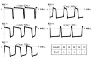
図7は、二次転写バイアスについて説明する波形図である。
図7(a)は転写に必要な大きさの電圧は印加するが、Dutyを50%より高く設定することで印加時間を短くし、トナーの過充電を防ぐことで、ハーフトーンを良好に転写できる理想波形である。図7(a)中の記号は、Vr:正の電圧のピーク値、Vt::負の電圧のピーク値、Voff:(Vr+Vt)/2、Vpp:Vr−Vt、Vave:Vr×Duty/100+Vt×(1−Duty)/100、A:Vtの持続時間、B:波形1周期の時間、Duty:(B−A)/B×100(%)をそれぞれ示す。
FIG. 7 is a waveform diagram illustrating the secondary transfer bias.
In FIG. 7A, a voltage of a magnitude necessary for transfer is applied, but by setting the duty higher than 50%, the application time is shortened, and overcharging of the toner is prevented, so that the halftone is transferred well. This is an ideal waveform. Symbols in FIG. 7A are Vr: peak value of positive voltage, Vt:: peak value of negative voltage, Voff: (Vr+Vt)/2, Vpp: Vr−Vt, Vave: Vr×Duty/100+Vt. X(1-Duty)/100, A: Vt duration, B: time of one waveform period, Duty: (B-A)/B x 100(%) are shown.
図7(b)は図7(a)の理想波形を狙って実際に出力された波形である。Vt:−4.8kV、Vr:1.2kV、Voff:−1.8kV、Vave:0.08kV、Vpp:6.0kV、Vtピークの持続時間A:0.10ms、波形の周期B:0.66ms、Duty:85%の波形の交流電圧を印加した。 FIG. 7B is a waveform actually output aiming at the ideal waveform of FIG. 7A. Vt: -4.8 kV, Vr: 1.2 kV, Voff: -1.8 kV, Vave: 0.08 kV, Vpp: 6.0 kV, Vt peak duration A: 0.10 ms, waveform period B: 0. An AC voltage having a waveform of 66 ms and Duty: 85% was applied.
実施形態の装置構成の実機を用いてトナー像の転写実験を実施した。実験条件は、環境:27℃/80%、用紙:コート紙=Mohawk Color Copy Gloss(商品名)270gsm(457mm×305mm)、プロセス線速:630mm/s、出力画像:Bkハーフトーン、二次転写ニップ幅:4mmである。なお、コート紙の転写時に限らず、普通紙や再生紙の転写時に実施形態で説明した二次転写バイアスを用いても良い。 A toner image transfer experiment was conducted using an actual machine having the apparatus configuration of the embodiment. Experimental conditions are: environment: 27°C/80%, paper: coated paper = Mohawk Color Copy Gloss (trade name) 270 gsm (457 mm x 305 mm), process linear velocity: 630 mm/s, output image: Bk halftone, secondary transfer Nip width: 4 mm. The secondary transfer bias described in the embodiment may be used not only when transferring the coated paper but also when transferring the plain paper or the recycled paper.
図8は、図7の波形の条件でDutyを10%から90%まで振った時の出力波形を示すものである。これらの波形でハーフトーン画像を出力し、官能評価のランク付けを行うと、Dutyが90%と70%ではランク5であり、50%でランク3、30%と10%でランク1であった。
FIG. 8 shows an output waveform when the duty is varied from 10% to 90% under the waveform condition of FIG. When halftone images were output with these waveforms and sensory evaluation was performed, the duty was 90% and 70%,
ランクは次のようにして評価した。十分なハーフトーンの濃度を得られている場合をランク5と評価した。ランク5に比べてやや薄いが、問題のない濃さが得られている場合を、ランク4として評価した。ランク4に比べてさらに薄く、ユーザーに提供する画質としては問題となる場合をランク3として評価した。ランク3に比べてさらに薄い場合をランク2とし、全体的に白っぽい場合やそれよりも薄い場合をランク1として評価した。ユーザーに提供できる画質の許容レベルとしては、ランク4以上である。
The rank was evaluated as follows.
図7で説明したように低Dutyの10%、30%では、(トナーを記録媒体に転写させる側=ここではマイナス側の)電圧を印加する時間が長く、トナー像が過充電され、転写性が悪くなった。一方、高Dutyの70%、90%では、上記電圧を印加する時間が短く、過充電が防げ、転写性が良くなった。 As described with reference to FIG. 7, at low duty of 10% and 30%, the time for applying the voltage (on the side where the toner is transferred to the recording medium=here, the negative side) is long, the toner image is overcharged, and the transferability is reduced. Became worse. On the other hand, at high duty of 70% and 90%, the time for applying the voltage was short, overcharge was prevented, and transferability was improved.
また、波形において、VrとVtで極性を反転させると、過充電をより確実に防げる。その理由は、紙が帯電している場合でも、0をまたぐことで充電を防ぐ向きに電界をつくるからである。 Further, in the waveform, if the polarities are inverted between Vr and Vt, overcharge can be prevented more reliably. The reason is that even when the paper is charged, it crosses over 0 to create an electric field in a direction to prevent charging.
図3、図4で説明したように、ベルト表面に粒子を分散させると、トナーの離型性が向上する。しかし、従来のようなACバイアス(Duty50%以下やDC定電流)を用いると、ハーフトーン画像について転写不良が起きる。その原因は、粒子の隙間から電流がもれてトナーが過充電されたためである。そこで、ベルト表面に粒子を分散させたベルトを用いる場合に、高Dutyの転写バイアスを用いることで上の問題が解決できる。これにより、離型性の向上と転写不良の防止ができる。
As described with reference to FIGS. 3 and 4, when the particles are dispersed on the surface of the belt, the releasability of the toner is improved. However, when an AC bias (
さらに、粒子に正帯電の粒子(メラミン)を用いると、マイナス要素の大きい転写バイアスと打ち消しあい、隙間から電流がもれるのを防止できる。これと高Duty波形を組み合わせることで、より確実にトナー過充電による画像不良を防止できる。粒子に負帯電の粒子(トスパール)を用いると、トナーの過充電が起きやすくなるが、高Duty波形を用いることで、転写不良を防止できる。 Furthermore, if positively charged particles (melamine) are used as the particles, it is possible to cancel the transfer bias having a large negative factor and to prevent current leakage from the gap. By combining this with a high duty waveform, it is possible to more reliably prevent image defects due to toner overcharge. When negatively charged particles (Tospearl) are used as the particles, overcharge of the toner easily occurs, but by using a high duty waveform, transfer failure can be prevented.
ベルト表面にウレタンやテフロン(登録商標)などをコートした、コート層を有するベルトに対しても、高Duty波形を用いることで、転写不良を防止できる。ポリイミドやポリアミドイミドなどの樹脂を複数積層したベルトに対しても、高Duty波形を用いることで、転写不良を防止できる。 Even for a belt having a coat layer in which the surface of the belt is coated with urethane or Teflon (registered trademark), the transfer failure can be prevented by using the high duty waveform. Even for a belt in which a plurality of resins such as polyimide and polyamideimide are laminated, it is possible to prevent transfer failure by using a high duty waveform.
なお、凹凸紙の溝部の転写性を確保するためには低DutyのAC転写(直流成分に交流成分を重畳した重畳転写)が効果的である。例えば、図8の低Duty波形(Duty=30%、10%)でVpp=12kV程度の波形を用いることで、レザック紙(商品名)等における溝部の転写性を確保する効果が得られる。 In order to secure the transferability of the groove portion of the concavo-convex paper, low-duty AC transfer (superposition transfer in which AC component is superposed on DC component) is effective. For example, by using a waveform having a low Duty waveform (Duty=30%, 10%) and Vpp=12 kV in FIG. 8, it is possible to obtain the effect of ensuring the transferability of the groove portion in the Resac paper (trade name) or the like.
さて、本実施形態のプリンタ500は、画像濃度を調整する画像調整モードを備えている。この画像調整モードにおいては、画像形成情報である信号を発するとともに、中間転写ベルト31上に画像濃度調整用のトナーパターン(以下、調整パターンと称する)を形成し、二次転写ニップNにおいて記録媒体ではなく、二次転写ベルト36上に調整パターンを転写する。画像調整モードでは、二次転写ベルト36上に転写された調整パターンを、二次転写ユニット41に設けたパターン検知センサ45によってその濃度を検知し、制御部によってパターン検知センサ45が検知した画像濃度情報に応じて、調整パターンの画像濃度が所定の値となるようにフィードバック制御する(いわゆるプロセスコントロール)。検知手段で検知する像担持体の状態とは、調整パターンの濃度の状態である。
Now, the
プロセスコントロールは、所定時間経過毎や所定枚数のプリント毎などの所定のタイミングで実施する。図9は、連続プリント(連続印刷)時の紙間における調整パターンの転写を説明するための模式図である。 The process control is performed at a predetermined timing such as a predetermined time elapses or a predetermined number of prints. FIG. 9 is a schematic diagram for explaining transfer of an adjustment pattern between sheets during continuous printing (continuous printing).
図9において、中間転写ベルト31には、順次用紙に転写される出力画像が担持されている。図では左から2番目の出力画像と3番目の出力画像の間にプロセスコントロール用の調整パターン910が担持されている。二次転写裏面ローラ33(図1)には、出力画像を用紙上に転写させるバイアス(画像部バイアス)が印加されるが、図に示すように、調整パターン910のところで(調整パターン910がある紙間で)バイアスが非画像部バイアスに切り替えられる。この非画像部バイアスの作用で、調整パターン910が中間転写ベルト31から二次転写ベルト36(図1)に転写される。本実施形態では、二次転写ベルト36に転写された調整パターン910をパターン検知センサ45(図1)で検知してプロセスコントロールを実施する。
In FIG. 9, an
このときのバイアス切り替えは、紙間の僅かな時間で、切り替えなければならない。紙間に相当する時間は、本実施形態のような高速機の場合、約20msec程度の短時間である。この短時間で狙いの非画像部バイアスに切り替わらなかった場合には、調整パターン910の転写不良が発生する恐れがあり、その場合には正確なプロセスコントロールが実施できず、良好な出力画像を得ることができない。
The bias switching at this time must be switched in a short time between sheets. The time corresponding to the paper interval is a short time of about 20 msec in the case of the high speed machine as in this embodiment. If the target non-image portion bias is not switched in this short time, transfer failure of the
従来制御では、短時間でバイアスを狙いの非画像部バイアス911に切り替えることが困難であり、調整パターンの転写不良が発生する恐れがある。短時間でのバイアス切替が難しい理由は、(1):バイアスを出力する電源の特性上、出力の立ち上がり時よりも立下り時のほうが時間がかかる(狙いの出力となるまでの時間が長くなる)。図示例では、画像部バイアス913から非画像部バイアス911への切り替え(図の下方から上方への切り替え)が立下りとなる。(2):転写ニップを構成するローラやベルトなどの部材がコンデンサとして機能し電荷を溜める、ためである。
In the conventional control, it is difficult to switch the bias to the target
上述したように、本実施形態では、調整パターン910を中間転写ベルト31から二次転写ベルト36に転写して、二次転写ベルト36上でパターン検知センサ45により検知している。したがって、転写バイアスを紙間で狙いの非画像部バイアスの値に素早く切り替えることで、調整パターン910を確実に転写することが可能となり、正確なプロセスコントロールを実施して、良好な出力画像を得ることができる。
As described above, in the present embodiment, the
図10は、実施形態におけるバイアス切替の制御例を説明する模式図である。図に示すように、画像部バイアス913から非画像部バイアス911へのバイアス切替に際し、画像部902の後端で補正バイアス(後端補正部バイアス914)を入れ、画像部バイアス913から後端補正部バイアス914を介して非画像部バイアス911へ切り替えている。補正バイアス(後端補正部バイアス914)は、バイアスを画像部バイアス913から非画像部バイアス911へ近づく方向に補正するものとする。また、後述するように、画像部バイアス913における定電流制御を、切替部915では定電圧制御に切り替える。
FIG. 10 is a schematic diagram illustrating a bias switching control example in the embodiment. As shown in the drawing, when the bias is switched from the
図11は、後端補正部バイアスを用いない場合の制御例を説明する模式図である。この場合、画像部902の後端で、画像部バイアス913から非画像部バイアス911へバイアスを切り替えている。この場合も画像部バイアス913における定電流制御を、切替部915では定電圧制御に切り替える。
FIG. 11 is a schematic diagram illustrating a control example when the rear end correction unit bias is not used. In this case, the bias is switched from the
図12は、図10のバイアス切替における電源制御の一例を示す模式図である。連続印刷を行った場合、画像部902の前後に非画像部901がある。非画像部901で調整パターンを中間転写ベルト31から二次転写ベルト36に転写させる。このとき、バイアスは非画像部バイアス911を印加する。
FIG. 12 is a schematic diagram showing an example of power supply control in the bias switching of FIG. When continuous printing is performed, there is a
本実施形態では、二次転写バイアスを印加する電源を、定電流制御1101と定電圧制御1102とに、定電圧切替信号1103で切替えることができるようになっている。この切替信号1103がONのとき、バイアス制御は定電圧制御1102になる。
In this embodiment, the power supply for applying the secondary transfer bias can be switched between the constant
図12の切替部915における制御は、定電流制御を0μAとして、定電圧切替信号1103を切替時間だけONにし、定電圧制御1102を−2.8kVとする。その後、定電圧切替信号1103をOFFにし、定電流制御1101を非画像部バイアスの−60μAとする。なお、画像部バイアス913は定電流制御とし、その値は−120μAである(定電圧制御1102は0kV)。また、後端補正部バイアス914も定電流制御とし、その値は−100μAである(定電圧制御1102は0kV)。
In the control in the
調整パターンが複数ある場合は、調整パターンごとに非画像部バイアスの値を変えても良い。
このような画像部から非画像部へのバイアス切替制御を行うことで、電源の応答遅れがなく所定の時間内に切替を行うことができ、非画像部で狙いのバイアスを印加することができる。その結果、調整パターンを確実に転写して正確なプロセスコントロールを実施することが可能となる。
When there are a plurality of adjustment patterns, the non-image part bias value may be changed for each adjustment pattern.
By performing such bias switching control from the image portion to the non-image portion, it is possible to perform switching within a predetermined time without a power supply response delay, and the target bias can be applied in the non-image portion. .. As a result, it becomes possible to reliably transfer the adjustment pattern and perform accurate process control.
なお、図示例では、非画像部バイアス911も画像部バイアス913と同様に定電流制御を行っている。その理由は、画像部と同じく中間転写ベルト31・二次転写裏面ローラ33、二次転写ベルト36、二次転写ローラ400の抵抗変動があっても、抵抗変動を吸収し転写ニップNに一定の電界を形成できるためである。
In the illustrated example, the
また、非画像部901に調整パターンがない場合は、画像部と同じバイアスをそのまま印加すればよい。これにより、次の出力画像先端でのバイアス不足を防ぐことができる。そして、調整パターンがない非画像部で画像部と異なるバイアスを印加する場合、画像部から非画像部へのバイアス切替は、図11の制御を行わず、画像部の定電流制御から非画像部の定電流制御に切り替えればよい。この場合には、制御が複雑とならず、制御負荷の増大を抑制できる。
If the
図13は、実施形態におけるバイアス切替制御を用いた場合と、従来の制御を用いた場合を比較する転写出力波形を示す図である。図13の(a)が実施形態の出力波形、(b)が従来例の出力波形である。図13(a)の波形図には、図12に示されている切替部915の実際の波形が示されている。
FIG. 13 is a diagram showing a transfer output waveform comparing the case where the bias switching control in the embodiment is used and the case where the conventional control is used. 13A shows the output waveform of the embodiment, and FIG. 13B shows the output waveform of the conventional example. The waveform diagram of FIG. 13A shows an actual waveform of the
図13(a)の実施形態では、画像部バイアス(−6.0kV)から非画像部バイアス(−2.8kV)への切替時間は22msecである。一方、図13(b)の従来例では、画像部バイアスから非画像部バイアスへの切替時間は140msecである。両者の比較から、切替部915の時間が実施形態では大幅に短縮されていることが分かる。
In the embodiment of FIG. 13A, the switching time from the image part bias (−6.0 kV) to the non-image part bias (−2.8 kV) is 22 msec. On the other hand, in the conventional example of FIG. 13B, the switching time from the image portion bias to the non-image portion bias is 140 msec. From the comparison between the two, it can be seen that the time of the
図14は、本発明によるバイアス切替制御を用いた場合と、従来の制御を用いた場合における、二次転写ベルト36上での調整パターン910の検知結果を示すグラフである。この図に示すように、本発明の制御を用いた場合、目標とする出力で検知できたが、従来の制御では目標出力よりも低い値しか検知することができなかった。すなわち、従来の制御では調整パターンの安定した転写が行われなかったため、不完全なトナーパッチ(調整パターン)をセンサで検知したためである。これに対し、実施形態の制御は、センサ出力が目標出力に一致している。よって、本願の制御を用いることで、転写バイアスの切替制御を狙い通り制御可能なことがわかる。
FIG. 14 is a graph showing the detection results of the
図15は、バイアス切替における電源制御の別例を示す模式図である。図12との違いは、切替部915で定電流制御1101を0μAにしないで、非画像部バイアス911と同じ−60μAにしている。その他は図12の制御例と同じである。
FIG. 15 is a schematic diagram showing another example of power supply control in bias switching. The difference from FIG. 12 is that the constant
本制御例では、切り替えの回数を図12の制御例より減らすことで、制御負荷の低減が可能となる。なお、定電圧切替信号1103がONのときは定電圧制御1102が出力され、定電流制御1101は出力されないので、制御上の矛盾は発生しない。
In this control example, the control load can be reduced by reducing the number of times of switching as compared with the control example of FIG. When the constant
図16は、バイアス切替における電源制御の更に別の例を示す模式図である。図12との違いは、定電圧切替信号1103がONになる以前から定電圧制御1102の出力をONにして、定電圧切替信号1103がOFFになった後に定電圧制御1102の出力をOFFにしている点である。その他は図12の制御例と同じである。
FIG. 16 is a schematic diagram showing still another example of power supply control in bias switching. The difference from FIG. 12 is that the output of the
定電圧制御1102にソフト遅延(制御ソフトの処理遅延)が生じたとしても、定電圧切替信号1103がONする前に定電圧制御1102をONすることで確実に定電圧電源を出力できる。さらに、定電圧制御1102の電源の応答遅れを無視した制御設計ができるので制御の仕組みが単純にできる。なお、定電圧切替信号1103がOFFのときは定電圧制御1102が出力されないので、制御上の矛盾は発生しない。
Even if a soft delay (processing delay of control software) occurs in the
図17は、図11のバイアス切替に対応する電源制御の一例を示す模式図である。
この場合、画像部後端での補正バイアス(後端補正部バイアス914)が無く、定電流制御1101を120μAから0μAに変更して、画像部バイアス913から非画像部バイアス911へ切り替えている。
FIG. 17 is a schematic diagram showing an example of power supply control corresponding to the bias switching of FIG.
In this case, there is no correction bias at the rear end of the image portion (rear end correction portion bias 914), the constant
図18は、調整パターンのある紙間部でのバイアス切替を画像基準及び用紙基準で詳しく説明する模式図である。
図18において、図の上段は、画像基準で領域を区分けして示すものである。また、図の中段は、用紙基準で領域を区分けして示すものである。また、図の下段は、転写バイアスを示すものである。この図において、非画像部901に調整パターン910が担持されている。
FIG. 18 is a schematic diagram for explaining in detail the bias switching in the sheet interval portion having the adjustment pattern on the image reference and the sheet reference.
In FIG. 18, the upper part of the figure shows the areas divided based on the image. In the middle of the figure, the areas are divided according to the paper. The lower part of the figure shows the transfer bias. In this figure, the
画像基準で説明すると、中間転写ベルト31(図1)上の画像部902には出力画像(プリント画像)が担持されている。また、先行する(図で左側の)画像部902と次の(図で右側の)画像部902との間の非画像部901(非画像領域)には調整パターン910が担持されている。そして、図の下段に示すように、画像部902には画像部バイアス913が印加される。また、調整パターン910部には非画像部バイアス911が印加される。つまり、転写バイアスが画像部バイアス913→非画像部バイアス911→画像部バイアス913と切り替えられる。画像部バイアス913から非画像部バイアス911への切替部が立下げ部Aであり、非画像部バイアス911から画像部バイアス913への切替部が立ち上げ部Bである。
Explaining on an image basis, an output image (print image) is carried on the
用紙基準で説明すると、画像領域は通常、用紙先端部に余白を設けることから、用紙先端よりも画像領域(画像部)の先端の方が後ろになる。用紙後端部では、後端部にも余白を設ける場合と、後端余白を設けずに用紙後端と画像部後端が一致する場合とがある。ここでは後端部にも余白を設ける場合である。図18において、先行の用紙902’と後続の用紙902’との間が紙間(紙間領域)901’となる。図示例では用紙先端部と用紙後端部の双方に余白を設けていることから、用紙の先端と後端が画像基準における非画像部901(非画像領域)にはみ出している。この場合も、転写バイアスが非画像部バイアス911と画像部バイアス913とに切り替えられる点は同じである。ここではバイアスは画像基準で切り替えているので、立下げ部Aの始まりは先行用紙の後端よりも早く、立ち上げ部Bの終わりは後続紙の先端よりも遅れたタイミングとなっている。
Explaining with reference to the paper, the image area is usually provided with a margin at the front end of the paper, so that the front end of the image area (image portion) is behind the front end of the paper. At the trailing edge of the sheet, there may be a case where a margin is provided also at the trailing edge, or there is a case where the trailing edge of the sheet and the trailing edge of the image portion are aligned without providing the trailing edge margin. Here is a case where a margin is also provided at the rear end portion. In FIG. 18, a space between the preceding paper 902' and the following paper 902' is a paper interval (paper interval region) 901'. In the illustrated example, since margins are provided at both the leading edge and the trailing edge of the sheet, the leading edge and the trailing edge of the sheet extend beyond the non-image portion 901 (non-image area) in the image reference. Also in this case, the transfer bias can be switched to the
先に説明したように、転写バイアスの切り替えに際し、電源特性及び転写ニップ構成の点から、バイアス出力の立ち上がり時よりも立下り時のほうが時間がかかる。図18の下段において、画像部バイアス913から非画像部バイアス911への切り替え(図の下方から上方への切り替え)が立下りとなる。つまり、立下げ部Aのほうが、立ち上げ部Bよりも狙いの出力となるまでの時間が長くなる。
As described above, when the transfer bias is switched, it takes more time at the time of falling of the bias output than at the time of rising of the bias output from the viewpoints of the power source characteristics and the transfer nip structure. In the lower part of FIG. 18, the switching from the
そこで、本実施形態では、調整パターン910を非画像領域(画像基準の場合)および紙間(用紙基準の場合)の中央ではなく、中央よりも後ろ寄り(図では右側)に位置するように設ける。具体的には感光体ドラム2(図1)上に調整パターン910を書き込むタイミングを制御することで、上記中央よりも後ろ寄りに調整パターン910を位置させる。すなわち、画像基準の場合ではL1>L2、用紙基準の場合にはL1’>L2’とする。このように調整パターン910を位置させることにより、バイアスを画像部バイアス913から非画像部バイアス911へ切り替える際の時間的な余裕度を増すことができる。それにより、図10〜図17で説明した上述のバイアス制御に加えて、時間的な余裕度も増大し、非画像部バイアス911をより確実に狙いの値へと切り替えることができる。
Therefore, in the present embodiment, the
なお、図18における立下げ部Aは図10〜図17における切替部915に相当するものであり、先に説明したように、切替部915では定電圧制御に切り替えている。それに加えて、調整パターン910がある場合には、調整パターン後のバイアス立ち上げ部B、すなわち非画像部バイアス911から画像部バイアス913への切替時も定電圧制御すると好適である。これにより、次画像先端部での転写不良(次画像先端部の濃度不足)を防止することができる。
Note that the falling unit A in FIG. 18 corresponds to the
ところで、本実施形態のプリンタは、電源投入時あるいは所定枚数のプリントを行う度に、色ずれ量補正処理も実施するようになっている。そして、この色ずれ量補正処理において、二次転写ベルト36の幅方向の一端部と他端部とにそれぞれ、図19に示すようなシェブロンパッチPVと呼ばれるY,M,C,Kの各色トナー像からなる色ずれ検知用画像を転写する。
By the way, the printer according to the present exemplary embodiment is configured to perform the color misregistration amount correction process each time the power is turned on or a predetermined number of prints are performed. Then, in this color misregistration correction process, Y, M, C, and K color toners called chevron patches PV as shown in FIG. 19 are respectively provided at one end and the other end in the width direction of the
シェブロンパッチPVは、図19に示すように、Y,M,C,Kの各色のトナー像を主走査方向から約45度傾けた姿勢で、副走査方向であるベルト移動方向に所定ピッチで並べたラインパターン群である。このシェブロンパッチPVの付着量は、0.3[mg/cm2]程度である。 As shown in FIG. 19, the chevron patch PV is arranged such that the toner images of Y, M, C, and K colors are inclined by about 45 degrees from the main scanning direction and arranged at a predetermined pitch in the belt moving direction, which is the sub-scanning direction. It is a group of line patterns. The attached amount of the chevron patch PV is about 0.3 [mg/cm 2 ].
そして、シェブロンパッチPV内の各色トナー像を検知することで、各色トナー像における主走査方向(感光体軸線方向)の位置、副走査方向(ベルト移動方向)の位置、主走査方向の倍率誤差、主走査方向からのスキューをそれぞれ検出する。ここで言う主走査方向とは、ポリゴンミラーでの反射に伴ってレーザー光が感光体表面上で位相する方向を示している。 Then, by detecting each color toner image in the chevron patch PV, a position in the main scanning direction (photoconductor axis direction), a position in the sub-scanning direction (belt moving direction), a magnification error in the main scanning direction, in each color toner image, Each skew from the main scanning direction is detected. The main scanning direction referred to here is the direction in which the laser light is in phase on the surface of the photoconductor as it is reflected by the polygon mirror.
このようなシェブロンパッチPV内のY,M,Cトナー像について、Kトナー像との検知時間差をパターン検知センサ45(図1)で読み取っていく。図19では、紙面上下方向が主走査方向に相当し、左から順に、Y,M,C,Kトナー像が並んだ後、これらとは姿勢が90度異なっているK,C,M,Yトナー像が更に並んでいる。 With respect to the Y, M, and C toner images in the chevron patch PV, the detection time difference from the K toner image is read by the pattern detection sensor 45 (FIG. 1). In FIG. 19, the vertical direction of the paper surface corresponds to the main scanning direction, and Y, M, C, and K toner images are arranged in order from the left, and K, C, M, and Y whose postures are different from these by 90 degrees. Further toner images are lined up.
基準色となるKとの検出時間差tyk、tmk、tckについての実測値と理論値との差に基づいて、各色トナー像の副走査方向のズレ量、即ちレジストズレ量を求める。そして、そのレジストズレ量に基づいて、光書込ユニット80のポリゴンミラー1面おき、即ち、1走査ラインピッチを1単位として、感光体2に対する光書込開始タイミングを補正して、各色トナー像のレジストズレを低減する。また、ベルト両端部間での副走査方向ズレ量の差に基づいて、各色トナー像の主走査方向からの傾き(スキュー)を求める。そして、その結果に基づいて、光学系反射ミラーの面倒れ補正を実施して、各色トナー像のスキューズレを低減する。
A deviation amount in the sub-scanning direction of each color toner image, that is, a registration deviation amount is obtained based on the difference between the measured value and the theoretical value of the detection time differences tyk, tmk, and tck from the reference color K. Then, based on the registration deviation amount, every other surface of the polygon mirror of the
以上のように、シェブロンパッチPV内における各トナー像を検知したタイミングに基づいて光書込開始タイミングや面倒れを補正してレジストズレやスキューズレを低減する処理が、色ずれ補正処理である。このような色ずれ補正処理により、温度変化などで各色トナー像の形成位置が経時的にずれていくことに起因する画像の色ずれの発生を抑えることができる。 As described above, the color misregistration correction process is a process for correcting the optical writing start timing and the surface misalignment to reduce the registration shift and the skew shift based on the timing of detecting each toner image in the chevron patch PV. By such a color misregistration correction process, it is possible to suppress the occurrence of color misregistration of an image due to the formation position of each color toner image being deviated with time due to temperature change or the like.
このような色ずれ検知用画像(調整パターン)が像担持体上で出力画像と出力画像の間にある場合、バイアスとして、出力画像が担持されている画像部に対応して印加される画像部バイアスと、画像部と前記画像部の間の非画像部に対応して印加される非画像部バイアスとで異なるバイアスを印加するとともに、画像部バイアスは定電流制御を行い、画像部バイアスから非画像部バイアスへの切り替え時に定電圧制御を行う。 When such an image for color shift detection (adjustment pattern) is present between the output images on the image carrier, an image part applied as a bias corresponding to the image part carrying the output image. A different bias is applied between the bias and the non-image part bias applied corresponding to the non-image part between the image part and the image part, and the image part bias performs constant current control so that the image part bias is not changed. Constant voltage control is performed when switching to the image part bias.
連続印刷時の紙間で色ずれ検知用画像を転写する場合、像担持体上の出力画像を転写する画像部バイアスと、紙間で色ずれ検知用画像を転写する非画像部バイアスとで異なるバイアスを印加するとともに、画像部バイアスは定電流制御を行い、画像部バイアスから非画像部バイアスへの切り替え時に定電圧制御を行う。
これにより、調整パターンを確実に転写することが可能となり、正確な調整制御を実施して、良好な出力画像を得ることができる。
When a color misregistration detection image is transferred between papers during continuous printing, the image part bias that transfers the output image on the image carrier differs from the non-image part bias that transfers the color misregistration detection image between papers. While applying the bias, the image portion bias performs constant current control, and performs constant voltage control when switching from the image portion bias to the non-image portion bias.
This makes it possible to reliably transfer the adjustment pattern, perform accurate adjustment control, and obtain a good output image.
ここまで説明したように、本発明の画像形成装置によれば、転写バイアスを画像部バイアスから狙いの非画像部バイアスに素早く切り替えることができる。そのため調整パターンを確実に転写することが可能となり、正確な調整制御を実施して、良好な出力画像を得ることができる。 As described above, according to the image forming apparatus of the present invention, the transfer bias can be quickly switched from the image portion bias to the target non-image portion bias. Therefore, the adjustment pattern can be reliably transferred, and accurate adjustment control can be performed to obtain a good output image.
なお、図5に示した電源構成では着脱可能な交流電源を備えるものであったが、電源構成は図示例に限定されるものではない。着脱式ではない交流電源を備えるものや、交流電源を備えていないもの(直流電源のみ備えるもの)であっても、本発明の効果は得られる。 The power supply configuration shown in FIG. 5 includes a removable AC power supply, but the power supply configuration is not limited to the illustrated example. The effect of the present invention can be obtained even if the AC power supply is not detachable, or if the AC power supply is not provided (only the DC power supply is provided).
また、本発明の画像形成装置において、調整パターンに対応する非画像部バイアスから後続の出力画像に対応する画像部バイアスへの切り替え時に定電圧制御を行うことで、調整パターン後の出力画像先端部の濃度不足を防止することができる。 Further, in the image forming apparatus of the present invention, constant voltage control is performed at the time of switching from the non-image portion bias corresponding to the adjustment pattern to the image portion bias corresponding to the subsequent output image, so that the output image front end portion after the adjustment pattern is It is possible to prevent the lack of concentration.
また、直流成分を出力する直流電源と交流成分を出力する交流電源を含む電源構成において、画像部バイアスから非画像部バイアスへの切り替え時に転写バイアスの直流成分について定電圧制御を行うことで、交流電源の影響による直流電源の応答性低下を抑制し、直流電源の出力を狙いの非画像部バイアスへと素早く切り替えることができる。 Further, in a power supply configuration including a DC power source that outputs a DC component and an AC power source that outputs an AC component, constant voltage control is performed on the DC component of the transfer bias at the time of switching from the image portion bias to the non-image portion bias. The responsiveness of the DC power supply due to the influence of the power supply can be suppressed, and the output of the DC power supply can be quickly switched to the target non-image area bias.
また、調整パターンと先行出力画像間の距離をL1とし、調整パターンと後続出力画像間の距離をL2とするとき、L1>L2であることにより、バイアスを画像部バイアスから非画像部バイアスへ切り替える際の時間的な余裕度を増すことができる。それにより、より確実に非画像部バイアスを狙いの値へと切り替えることができる。 When the distance between the adjustment pattern and the preceding output image is L1 and the distance between the adjustment pattern and the subsequent output image is L2, the bias is switched from the image portion bias to the non-image portion bias because L1>L2. The time margin can be increased. Thereby, the non-image portion bias can be more surely switched to the target value.
また、調整パターンと先行記録媒体間の距離をL1’とし、調整パターンと後続記録媒体間の距離をL2’とするとき、L1’>L2’であることにより、バイアスを画像部バイアスから非画像部バイアスへ切り替える際の時間的な余裕度を増すことができる。それにより、より確実に非画像部バイアスを狙いの値へと切り替えることができる。 Further, when the distance between the adjustment pattern and the preceding recording medium is L1′ and the distance between the adjustment pattern and the subsequent recording medium is L2′, L1′>L2′, so that the bias is changed from the image portion bias to the non-image. It is possible to increase the time margin when switching to the partial bias. Thereby, the non-image portion bias can be more surely switched to the target value.
また、像担持体上で出力画像と出力画像の間に調整パターンが無い場合は、画像部バイアスと非画像部バイアスを同一とすることにより、次画像先端部での転写不良(次画像先端部の濃度不足)を防止することができる。 Further, when there is no adjustment pattern between the output images on the image carrier, the image portion bias and the non-image portion bias are made to be the same, so that the transfer failure at the leading edge of the next image (leading edge of the next image) (Insufficient concentration) can be prevented.
また、像担持体としての中間転写部材と、該中間転写部材との間に転写ニップを形成する二次転写部材とを有し、調整パターンを中間転写部材から二次転写部材に転写し、二次転写部材上で調整パターンを検知して調整制御を行う構成において、調整パターンが確実に二次転写部材に転写され、正確な調整制御を行うことが可能となる。 Further, it has an intermediate transfer member as an image carrier and a secondary transfer member which forms a transfer nip between the intermediate transfer member and the intermediate transfer member, and transfers the adjustment pattern from the intermediate transfer member to the secondary transfer member. In the configuration in which the adjustment pattern is detected on the next transfer member and the adjustment control is performed, the adjustment pattern is reliably transferred to the secondary transfer member, and accurate adjustment control can be performed.
また、画像部バイアスから調整パターンに対応する非画像部バイアスへの切り替えに際し、バイアスを非画像部バイアスに近づく方向の補正バイアスを介して切り替えることで、より確実に非画像部バイアスを狙いの値へと切り替えることができる。 Further, when switching from the image part bias to the non-image part bias corresponding to the adjustment pattern, the bias is switched via the correction bias in the direction approaching the non-image part bias, so that the non-image part bias is more reliably targeted. You can switch to.
また、像担持体に界面があるため切替時間が単層のベルトよりも長くなる多層構造の像担持体を用いる場合であっても、転写バイアスを画像部バイアスから狙いの非画像部バイアスに素早く切り替えることができる。 Further, even when using a multi-layered image carrier in which the switching time is longer than that of a single-layer belt due to the interface of the image carrier, the transfer bias can be quickly changed from the image portion bias to the target non-image portion bias. You can switch.
また、像担持体の弾性層の表面に複数の粒子が分散されている構成を用いる場合、粒子がコンデンサとなるため切替時間が単層のベルトよりも長くなるが、その場合であっても、転写バイアスを画像部バイアスから狙いの非画像部バイアスに素早く切り替えることができる。 Further, when using a configuration in which a plurality of particles are dispersed on the surface of the elastic layer of the image carrier, the switching time becomes longer than the single-layer belt because the particles serve as a capacitor, but even in that case, The transfer bias can be quickly switched from the image portion bias to the target non-image portion bias.
また、弾性層の表面に分散された粒子の帯電特性が正である場合であっても、転写バイアスを画像部バイアスから狙いの非画像部バイアスに素早く切り替えることができる。
また、弾性層の表面に分散された粒子の帯電特性が負である場合であっても、転写バイアスを画像部バイアスから狙いの非画像部バイアスに素早く切り替えることができる。
In addition, even when the charging characteristics of the particles dispersed on the surface of the elastic layer are positive, the transfer bias can be quickly switched from the image portion bias to the target non-image portion bias.
Further, even when the charging characteristics of the particles dispersed on the surface of the elastic layer are negative, the transfer bias can be quickly switched from the image portion bias to the target non-image portion bias.
また、弾性層の上にコート層が形成されている場合であっても、転写バイアスを画像部バイアスから狙いの非画像部バイアスに素早く切り替えることができる。
また、像担持体の複数層が複数の樹脂層を含む場合であっても、転写バイアスを画像部バイアスから狙いの非画像部バイアスに素早く切り替えることができる。
Further, even when the coat layer is formed on the elastic layer, the transfer bias can be quickly switched from the image portion bias to the target non-image portion bias.
Further, even when the plurality of layers of the image carrier include a plurality of resin layers, the transfer bias can be quickly switched from the image portion bias to the target non-image portion bias.
以上、本発明を図示例により説明したが、本発明はこれに限定されるものではない。転写部の構成は適宜な構成を採用可能であり、また、適宜な構成の電源を使用可能である。
画像形成装置各部の構成も任意であり、タンデム式における各色作像ユニットの並び順などは任意である。また、4色機に限らず、3色のトナーを用いるフルカラー機や、2色のトナーによる多色機にも本発明を適用することができる。もちろん、画像形成装置としてはプリンタに限らず、複写機やファクシミリ、あるいは複数の機能を備える複合機であっても良い。
Although the present invention has been described above with reference to the illustrated example, the present invention is not limited to this. The transfer unit may have an appropriate structure, and a power source having an appropriate structure may be used.
The configuration of each unit of the image forming apparatus is also arbitrary, and the arrangement order of the color image forming units in the tandem system is arbitrary. Further, the present invention can be applied not only to a four-color machine but also to a full-color machine using three-color toner and a multi-color machine using two-color toner. Of course, the image forming apparatus is not limited to the printer, but may be a copying machine, a facsimile, or a multi-function peripheral having a plurality of functions.
1 画像形成ユニット
30 転写ユニット
31 中間転写ベルト(像担持体)
41 二次転写ユニット
36 二次転写ベルト
39 バイアス電源
45 パターン検知センサ
80 光書込ユニット
110 直流電源
140 交流電源
200 電源制御部
500 プリンタ
P 用紙(記録媒体)
N 二次転写ニップ
1
41
N Secondary transfer nip
Claims (14)
前記像担持体との間に転写ニップを形成する転写部材と、
前記転写ニップで前記トナー像を記録媒体へ転写するための転写バイアスを出力可能な電源と、
前記電源を制御する制御手段と、を備える画像形成装置において、
前記像担持体上で出力画像と出力画像の間に調整パターンがある場合、前記バイアスとして、前記出力画像が担持されている画像部に対応して印加される画像部バイアスと、前記画像部と前記画像部の間の非画像部に対応して印加される非画像部バイアスとで異なるバイアスを印加するとともに、
前記画像部バイアスは定電流制御を行い、前記画像部バイアスから前記非画像部バイアスへの切り替え時に定電圧制御を行うこと、及び、
前記画像部バイアスから前記調整パターンに対応する前記非画像部バイアスへの切り替えに際し、バイアスを前記非画像部バイアスに近づく方向の補正バイアスを介して切り替えることを特徴とする画像形成装置。 An image carrier on which a toner image is carried,
A transfer member that forms a transfer nip with the image carrier,
A power supply capable of outputting a transfer bias for transferring the toner image onto a recording medium at the transfer nip;
An image forming apparatus comprising: a control unit that controls the power source,
When there is an adjustment pattern between output images on the image carrier, as the bias, an image part bias applied corresponding to the image part on which the output image is carried, and the image part. While applying a different bias from the non-image portion bias applied corresponding to the non-image portion between the image portion,
The image section bias performs constant current control, and performs constant voltage control when switching from the image section bias to the non-image section bias , and
An image forming apparatus characterized in that , when switching from the image part bias to the non-image part bias corresponding to the adjustment pattern, the bias is switched via a correction bias in a direction approaching the non-image part bias .
前記像担持体との間に転写ニップを形成する転写部材と、
前記転写ニップで前記トナー像を記録媒体へ転写するための転写バイアスを出力可能な電源と、
前記電源を制御する制御手段と、を備える画像形成装置において、
連続印刷時の紙間で調整パターンを転写する場合、前記像担持体上の出力画像を転写する画像部バイアスと、前記紙間で前記調整パターンを転写する非画像部バイアスとで異なるバイアスを印加するとともに、
前記画像部バイアスは定電流制御を行い、前記画像部バイアスから前記非画像部バイアスへの切り替え時に定電圧制御を行うこと、及び、
前記画像部バイアスから前記調整パターンに対応する前記非画像部バイアスへの切り替えに際し、バイアスを前記非画像部バイアスに近づく方向の補正バイアスを介して切り替えることを特徴とする画像形成装置。 An image carrier on which a toner image is carried,
A transfer member that forms a transfer nip with the image carrier,
A power supply capable of outputting a transfer bias for transferring the toner image onto a recording medium at the transfer nip;
An image forming apparatus comprising: a control unit that controls the power source,
When the adjustment pattern is transferred between the sheets during continuous printing, different biases are applied between the image portion bias that transfers the output image on the image carrier and the non-image portion bias that transfers the adjustment pattern between the sheets. Along with
The image section bias performs constant current control, and performs constant voltage control when switching from the image section bias to the non-image section bias , and
An image forming apparatus characterized in that , when switching from the image part bias to the non-image part bias corresponding to the adjustment pattern, the bias is switched via a correction bias in a direction approaching the non-image part bias .
前記転写バイアスの直流成分について前記定電圧制御を行うことを特徴とする、請求項1〜3のいずれか1項に記載の画像形成装置。 The power source includes a direct current power source for outputting a direct current component and an alternating current power source for outputting an alternating current component,
The image forming apparatus according to claim 1, wherein the constant voltage control is performed on the DC component of the transfer bias.
Priority Applications (2)
| Application Number | Priority Date | Filing Date | Title |
|---|---|---|---|
| JP2016098007A JP6728958B2 (en) | 2016-05-16 | 2016-05-16 | Image forming device |
| US15/596,365 US10101690B2 (en) | 2016-05-16 | 2017-05-16 | Image forming apparatus |
Applications Claiming Priority (1)
| Application Number | Priority Date | Filing Date | Title |
|---|---|---|---|
| JP2016098007A JP6728958B2 (en) | 2016-05-16 | 2016-05-16 | Image forming device |
Publications (2)
| Publication Number | Publication Date |
|---|---|
| JP2017207547A JP2017207547A (en) | 2017-11-24 |
| JP6728958B2 true JP6728958B2 (en) | 2020-07-22 |
Family
ID=60297600
Family Applications (1)
| Application Number | Title | Priority Date | Filing Date |
|---|---|---|---|
| JP2016098007A Active JP6728958B2 (en) | 2016-05-16 | 2016-05-16 | Image forming device |
Country Status (2)
| Country | Link |
|---|---|
| US (1) | US10101690B2 (en) |
| JP (1) | JP6728958B2 (en) |
Families Citing this family (9)
| Publication number | Priority date | Publication date | Assignee | Title |
|---|---|---|---|---|
| US10642203B2 (en) * | 2017-04-10 | 2020-05-05 | Canon Kabushiki Kaisha | Image forming apparatus |
| JP2019159208A (en) | 2018-03-15 | 2019-09-19 | 株式会社リコー | Image forming apparatus and control method |
| US10816919B2 (en) * | 2018-03-16 | 2020-10-27 | Ricoh Company, Ltd. | Power source device, power source control method, and image forming apparatus |
| JP7206667B2 (en) * | 2018-07-20 | 2023-01-18 | 富士フイルムビジネスイノベーション株式会社 | image forming device |
| JP2020042086A (en) * | 2018-09-07 | 2020-03-19 | 富士ゼロックス株式会社 | Transfer device and image forming device |
| JP7143779B2 (en) * | 2019-02-15 | 2022-09-29 | コニカミノルタ株式会社 | image forming device |
| US11494602B2 (en) | 2020-09-15 | 2022-11-08 | Ricoh Company, Ltd. | Image forming apparatus |
| US11592774B2 (en) * | 2020-12-14 | 2023-02-28 | Ricoh Company, Ltd. | Image forming apparatus and image forming method |
| JP7823449B2 (en) | 2022-03-18 | 2026-03-04 | 株式会社リコー | Image forming device |
Family Cites Families (49)
| Publication number | Priority date | Publication date | Assignee | Title |
|---|---|---|---|---|
| JP2614317B2 (en) * | 1989-06-20 | 1997-05-28 | キヤノン株式会社 | Image forming device |
| JPH08328401A (en) * | 1995-05-26 | 1996-12-13 | Ricoh Co Ltd | Image forming device |
| US6014158A (en) * | 1997-04-29 | 2000-01-11 | Eastman Kodak Company | Transfer roller electrical bias control |
| JP3191727B2 (en) * | 1997-05-21 | 2001-07-23 | 富士ゼロックス株式会社 | Image forming apparatus and image forming method |
| JP2002072713A (en) * | 2000-08-28 | 2002-03-12 | Konica Corp | Image forming device |
| JP4027287B2 (en) * | 2002-09-30 | 2007-12-26 | キヤノン株式会社 | Image forming apparatus |
| US7398032B2 (en) * | 2004-12-13 | 2008-07-08 | Canon Kabushiki Kaisha | Image forming apparatus featuring first and second cleaners operable on the basis of an interval of an image forming process during a continuous image forming process |
| JP2006349967A (en) * | 2005-06-15 | 2006-12-28 | Ricoh Co Ltd | Image forming apparatus |
| JP2007171600A (en) * | 2005-12-22 | 2007-07-05 | Seiko Epson Corp | Image forming method |
| JP2008058585A (en) * | 2006-08-31 | 2008-03-13 | Matsushita Electric Ind Co Ltd | Image forming apparatus |
| JP5058723B2 (en) * | 2007-09-04 | 2012-10-24 | キヤノン株式会社 | Image forming apparatus |
| JP2010072074A (en) * | 2008-09-16 | 2010-04-02 | Canon Inc | Image forming apparatus |
| JP5393284B2 (en) * | 2009-06-18 | 2014-01-22 | キヤノン株式会社 | Image forming apparatus |
| JP5464487B2 (en) | 2010-03-18 | 2014-04-09 | 株式会社リコー | Cleaning device and image forming apparatus |
| JP5707787B2 (en) * | 2010-06-10 | 2015-04-30 | 株式会社リコー | Transfer device and image forming apparatus using the same |
| US8532518B2 (en) * | 2010-07-29 | 2013-09-10 | Canon Kabushiki Kaisha | Image forming apparatus |
| US20120027432A1 (en) * | 2010-07-30 | 2012-02-02 | Brown Kenneth J | Electrophotographic developer flow rate measurement |
| JP5623175B2 (en) * | 2010-07-30 | 2014-11-12 | キヤノン株式会社 | High voltage generator, image forming apparatus, and voltage control method for high voltage generator |
| JP5585870B2 (en) | 2010-08-20 | 2014-09-10 | 株式会社リコー | Image forming apparatus |
| JP5492025B2 (en) * | 2010-08-31 | 2014-05-14 | 株式会社沖データ | Image forming apparatus |
| JP5790986B2 (en) | 2011-03-04 | 2015-10-07 | 株式会社リコー | Image forming apparatus |
| JP5888587B2 (en) * | 2011-03-07 | 2016-03-22 | 株式会社リコー | Image forming apparatus |
| JP5954939B2 (en) * | 2011-05-30 | 2016-07-20 | キヤノン株式会社 | Image forming apparatus |
| JP5678841B2 (en) | 2011-06-02 | 2015-03-04 | 株式会社リコー | Image forming apparatus |
| JP5900056B2 (en) | 2011-06-08 | 2016-04-06 | 株式会社リコー | Image forming apparatus |
| JP6003206B2 (en) | 2011-06-24 | 2016-10-05 | 株式会社リコー | Image forming apparatus, power supply control apparatus, image forming system, transfer method, and transfer program |
| JP5932281B2 (en) * | 2011-10-07 | 2016-06-08 | キヤノン株式会社 | Image forming apparatus |
| JP5936345B2 (en) * | 2011-12-19 | 2016-06-22 | キヤノン株式会社 | Image forming apparatus |
| JP5721005B2 (en) * | 2011-12-26 | 2015-05-20 | 株式会社リコー | Image forming apparatus |
| JP6168815B2 (en) * | 2012-04-03 | 2017-07-26 | キヤノン株式会社 | Image forming apparatus |
| JP6168817B2 (en) * | 2012-04-03 | 2017-07-26 | キヤノン株式会社 | Image forming apparatus |
| JP2014016479A (en) * | 2012-07-09 | 2014-01-30 | Fuji Xerox Co Ltd | Image forming apparatus and bias power supply device |
| JP2014123004A (en) | 2012-12-21 | 2014-07-03 | Kyocera Document Solutions Inc | Image forming apparatus |
| JP6082611B2 (en) * | 2013-02-05 | 2017-02-15 | シャープ株式会社 | Transfer device and image forming apparatus |
| JP6149512B2 (en) | 2013-05-01 | 2017-06-21 | 株式会社リコー | Image forming apparatus |
| EP2821858B1 (en) | 2013-05-01 | 2020-06-03 | Ricoh Company, Ltd. | Image forming apparatus |
| JP6286868B2 (en) | 2013-05-01 | 2018-03-07 | 株式会社リコー | Image forming apparatus |
| JP6270125B2 (en) * | 2013-08-02 | 2018-01-31 | 株式会社リコー | Image forming apparatus |
| JP2015194663A (en) * | 2013-10-11 | 2015-11-05 | 株式会社リコー | Transfer device and image forming apparatus |
| JP2016006471A (en) * | 2014-05-30 | 2016-01-14 | 株式会社リコー | Image forming apparatus |
| JP2016033639A (en) | 2014-07-30 | 2016-03-10 | 株式会社リコー | Image forming apparatus |
| JP2016038568A (en) | 2014-08-08 | 2016-03-22 | 株式会社リコー | Image forming apparatus |
| JP6489409B2 (en) | 2014-10-15 | 2019-03-27 | 株式会社リコー | Image forming apparatus |
| JP2016109969A (en) | 2014-12-09 | 2016-06-20 | 株式会社リコー | Image formation device |
| US9395658B2 (en) | 2014-12-09 | 2016-07-19 | Ricoh Company, Ltd. | Image forming apparatus |
| US9817341B2 (en) | 2015-03-18 | 2017-11-14 | Ricoh Company, Ltd. | Image forming apparatus |
| US9740156B2 (en) | 2015-03-19 | 2017-08-22 | Ricoh Company, Ltd. | Image forming apparatus that adjusts a transfer bias according to surface properties of a transfer target |
| JP2016177044A (en) | 2015-03-19 | 2016-10-06 | 株式会社リコー | Image forming apparatus |
| JP6492956B2 (en) | 2015-05-15 | 2019-04-03 | 株式会社リコー | Image forming apparatus |
-
2016
- 2016-05-16 JP JP2016098007A patent/JP6728958B2/en active Active
-
2017
- 2017-05-16 US US15/596,365 patent/US10101690B2/en active Active
Also Published As
| Publication number | Publication date |
|---|---|
| JP2017207547A (en) | 2017-11-24 |
| US20170329263A1 (en) | 2017-11-16 |
| US10101690B2 (en) | 2018-10-16 |
Similar Documents
| Publication | Publication Date | Title |
|---|---|---|
| JP6728958B2 (en) | Image forming device | |
| US9720355B2 (en) | Image forming apparatus | |
| JP6492956B2 (en) | Image forming apparatus | |
| JP2016109969A (en) | Image formation device | |
| US9766575B2 (en) | Image forming apparatus | |
| JP2014010383A (en) | Transfer device and image forming device | |
| US9535376B2 (en) | Image forming apparatus that switches transfer bias based on detected environment condition | |
| JP2016177044A (en) | Image forming apparatus | |
| US10067454B2 (en) | Image forming apparatus | |
| JP6452041B2 (en) | Image forming apparatus | |
| US9817341B2 (en) | Image forming apparatus | |
| JP6555571B2 (en) | Image forming apparatus | |
| JP7066981B2 (en) | Image forming device | |
| JP6593699B2 (en) | Image forming apparatus | |
| JP2016110013A (en) | Image formation device | |
| JP2017194667A (en) | Image forming apparatus | |
| JP6641617B2 (en) | Image forming device | |
| JP2016114913A (en) | Image formation device | |
| JP2016177062A (en) | Image forming apparatus | |
| JP2017016060A (en) | Image forming apparatus | |
| JP2016188991A (en) | Image forming apparatus | |
| JP6653074B2 (en) | Image forming device | |
| JP6784187B2 (en) | Image forming device | |
| JP2017191248A (en) | Image forming apparatus | |
| JP6459039B2 (en) | Image forming apparatus |
Legal Events
| Date | Code | Title | Description |
|---|---|---|---|
| A621 | Written request for application examination |
Free format text: JAPANESE INTERMEDIATE CODE: A621 Effective date: 20190208 |
|
| RD02 | Notification of acceptance of power of attorney |
Free format text: JAPANESE INTERMEDIATE CODE: A7422 Effective date: 20191025 |
|
| A977 | Report on retrieval |
Free format text: JAPANESE INTERMEDIATE CODE: A971007 Effective date: 20191127 |
|
| A131 | Notification of reasons for refusal |
Free format text: JAPANESE INTERMEDIATE CODE: A131 Effective date: 20191203 |
|
| A521 | Request for written amendment filed |
Free format text: JAPANESE INTERMEDIATE CODE: A523 Effective date: 20200123 |
|
| TRDD | Decision of grant or rejection written | ||
| A01 | Written decision to grant a patent or to grant a registration (utility model) |
Free format text: JAPANESE INTERMEDIATE CODE: A01 Effective date: 20200602 |
|
| A61 | First payment of annual fees (during grant procedure) |
Free format text: JAPANESE INTERMEDIATE CODE: A61 Effective date: 20200615 |
|
| R151 | Written notification of patent or utility model registration |
Ref document number: 6728958 Country of ref document: JP Free format text: JAPANESE INTERMEDIATE CODE: R151 |