JP6726362B2 - Analog-digital converter and solid-state image sensor - Google Patents
Analog-digital converter and solid-state image sensor Download PDFInfo
- Publication number
- JP6726362B2 JP6726362B2 JP2019525394A JP2019525394A JP6726362B2 JP 6726362 B2 JP6726362 B2 JP 6726362B2 JP 2019525394 A JP2019525394 A JP 2019525394A JP 2019525394 A JP2019525394 A JP 2019525394A JP 6726362 B2 JP6726362 B2 JP 6726362B2
- Authority
- JP
- Japan
- Prior art keywords
- data
- signal
- analog
- bit
- unit
- Prior art date
- Legal status (The legal status is an assumption and is not a legal conclusion. Google has not performed a legal analysis and makes no representation as to the accuracy of the status listed.)
- Active
Links
Images


Classifications
-
- H—ELECTRICITY
- H04—ELECTRIC COMMUNICATION TECHNIQUE
- H04N—PICTORIAL COMMUNICATION, e.g. TELEVISION
- H04N25/00—Circuitry of solid-state image sensors [SSIS]; Control thereof
- H04N25/60—Noise processing, e.g. detecting, correcting, reducing or removing noise
-
- H—ELECTRICITY
- H03—ELECTRONIC CIRCUITRY
- H03M—CODING; DECODING; CODE CONVERSION IN GENERAL
- H03M1/00—Analogue/digital conversion; Digital/analogue conversion
- H03M1/06—Continuously compensating for, or preventing, undesired influence of physical parameters
- H03M1/08—Continuously compensating for, or preventing, undesired influence of physical parameters of noise
- H03M1/0863—Continuously compensating for, or preventing, undesired influence of physical parameters of noise of switching transients, e.g. glitches
- H03M1/0872—Continuously compensating for, or preventing, undesired influence of physical parameters of noise of switching transients, e.g. glitches by disabling changes in the output during the transitions, e.g. by holding or latching
-
- H—ELECTRICITY
- H04—ELECTRIC COMMUNICATION TECHNIQUE
- H04N—PICTORIAL COMMUNICATION, e.g. TELEVISION
- H04N25/00—Circuitry of solid-state image sensors [SSIS]; Control thereof
- H04N25/70—SSIS architectures; Circuits associated therewith
- H04N25/71—Charge-coupled device [CCD] sensors; Charge-transfer registers specially adapted for CCD sensors
- H04N25/75—Circuitry for providing, modifying or processing image signals from the pixel array
-
- H—ELECTRICITY
- H04—ELECTRIC COMMUNICATION TECHNIQUE
- H04N—PICTORIAL COMMUNICATION, e.g. TELEVISION
- H04N25/00—Circuitry of solid-state image sensors [SSIS]; Control thereof
- H04N25/70—SSIS architectures; Circuits associated therewith
- H04N25/76—Addressed sensors, e.g. MOS or CMOS sensors
- H04N25/77—Pixel circuitry, e.g. memories, A/D converters, pixel amplifiers, shared circuits or shared components
- H04N25/772—Pixel circuitry, e.g. memories, A/D converters, pixel amplifiers, shared circuits or shared components comprising A/D, V/T, V/F, I/T or I/F converters
-
- H—ELECTRICITY
- H03—ELECTRONIC CIRCUITRY
- H03M—CODING; DECODING; CODE CONVERSION IN GENERAL
- H03M1/00—Analogue/digital conversion; Digital/analogue conversion
- H03M1/12—Analogue/digital converters
- H03M1/1205—Multiplexed conversion systems
- H03M1/123—Simultaneous, i.e. using one converter per channel but with common control or reference circuits for multiple converters
-
- H—ELECTRICITY
- H03—ELECTRONIC CIRCUITRY
- H03M—CODING; DECODING; CODE CONVERSION IN GENERAL
- H03M1/00—Analogue/digital conversion; Digital/analogue conversion
- H03M1/12—Analogue/digital converters
- H03M1/50—Analogue/digital converters with intermediate conversion to time interval
- H03M1/56—Input signal compared with linear ramp
-
- H—ELECTRICITY
- H03—ELECTRONIC CIRCUITRY
- H03M—CODING; DECODING; CODE CONVERSION IN GENERAL
- H03M7/00—Conversion of a code where information is represented by a given sequence or number of digits to a code where the same, similar or subset of information is represented by a different sequence or number of digits
- H03M7/14—Conversion to or from non-weighted codes
- H03M7/16—Conversion to or from unit-distance codes, e.g. Gray code, reflected binary code
Description
本発明は、CMOSイメージセンサなどの固体撮像素子に搭載され得るアナログデジタル変換器、およびそれを備えた固体撮像素子に関する。 The present invention relates to an analog-digital converter that can be mounted on a solid-state image sensor such as a CMOS image sensor, and a solid-state image sensor including the analog-digital converter.
従来のCMOSイメージセンサは、行列状に配置された画素ごとに、浮遊拡散層およびアンプを有する。CMOSイメージセンサの出力は、画素配列の中のある一行を選択し、それらを同時に列方向へと読み出すような列並列出力型が主流である。列方向に読み出された出力は、列ごとにアナログデジタル変換器にてデジタル信号に変換される。 A conventional CMOS image sensor has a floating diffusion layer and an amplifier for each pixel arranged in a matrix. The output of the CMOS image sensor is mainly of a column parallel output type in which one row in the pixel array is selected and read out in the column direction at the same time. The output read in the column direction is converted into a digital signal by an analog-digital converter for each column.
列並列出力型のCMOSイメージセンサに搭載されるアナログデジタル変換器について、従来、さまざまな構成ものが提案されている。中でも、初期状態と信号蓄積後の2つのデータをそれぞれアナログデジタル変換し、それぞれを減算処理(デジタルCDS)することによって、低ノイズ特性を実現した構成のアナログデジタル変換器が主流である。たとえば特許文献1には、上位ビットと下位ビットとで回路構成を変えることによって、消費電流および回路面積の最適化をはかる手法が開示されている。
Conventionally, various configurations of analog-digital converters mounted on a column parallel output type CMOS image sensor have been proposed. Among them, the mainstream is an analog-to-digital converter having a configuration that realizes low noise characteristics by performing analog-digital conversion on each of two data in the initial state and after signal accumulation and performing subtraction processing (digital CDS) on each. For example,
図7は、特許文献1に開示される従来のアナログデジタル変換器が搭載された固体撮像素子101の構成例を示すブロック図である。この図に示すように、固体撮像素子101は、画素部102、行選択回路103、参照電圧生成部104、カウンタ生成部105、アナログデジタル変換部(ADC部)106、列選択回路107、および信号処理部108を備えている。画素部102は、複数の単位画素121を備えている。ADC部106は、複数のアナログデジタル変換器(ADC)161を備えている。それぞれのADC161は、比較器162、下位ビットラッチ部163、および上位ビットカウンタ部164を備えている。
FIG. 7 is a block diagram showing a configuration example of a solid-state imaging device 101 equipped with a conventional analog-digital converter disclosed in
行選択回路103は、画素部102内の複数の行のうちいずれか1行分の単位画素121を選択する。選択された1行分の単位画素121は、入射光をアナログ信号に変換し、対応する垂直信号線122を通じて、対応するADC部106にアナログ信号を転送する。
The
参照電圧生成部104は、基準クロックに基づいて変動する参照電圧を生成する。比較器162は、入力されたアナログ信号電圧と、参照電圧と比較し、参照電圧がアナログ信号電圧を上回った時点で、出力信号を反転させる。カウンタ生成部105は、カウンタデータ151を生成する。下位ビットラッチ部163は、比較器162の出力信号が反転する時点をトリガとして、カウンタデータ151をラッチする。下位ビットラッチ部163は、キャリー信号165を生成する。上位ビットカウンタ部164は、キャリー信号165に応答して上位ビットをカウントする。
The
このように、図7に示す従来の固体撮像素子101は、データ遷移の多い下位ビットをカウントせず、カウント生成部105によって生成されたカウントデータ151をラッチする。これにより低消費電流化を実現することができる。さらに、上位ビットをバイナリカウンタとすることによって、即時に減算処理を実施できるので、固体撮像素子101の回路規模を縮小することができる。
As described above, the conventional solid-state imaging device 101 shown in FIG. 7 does not count the lower bits with many data transitions and latches the count data 151 generated by the
図7に示す従来の固体撮像素子101では、カウントデータ151をラッチしたデータと、キャリー信号165との間で、ビットの不整合を起こす可能性がある。このため、カウント生成部105によって生成されたマスク信号152を使用して、キャリー信号165を取り込む時点を制御する必要がる。また、マスク信号152をカウントデータ151から生成しなければならない場合もある。これらのことから、ADC161の回路構成および設計を簡素化できない問題が生ずる。
In the conventional solid-state imaging device 101 shown in FIG. 7, a bit mismatch may occur between the data in which the count data 151 is latched and the carry signal 165. Therefore, it is necessary to use the mask signal 152 generated by the
本発明は前記の課題を解決するためになされたものであり、その目的は、アナログデジタル変換器の回路構成および設計を簡素化することにある。 The present invention has been made to solve the above problems, and an object thereof is to simplify the circuit configuration and design of an analog-digital converter.
本発明の一態様に係るアナログデジタル変換器は、前記の課題を解決するために、少なくとも1つの列または少なくとも1つの単位画素ごとに配置され、入力されたアナログ信号をデジタル信号に変換するアナログデジタル変換器であって、前記アナログ信号の電圧と、基準クロックに対応して電圧値が変化する参照電圧とを比較する比較器と、前記比較器の出力が反転したことをトリガとして、前記基準クロックに対応したグレイコードデータを下位ビットとしてラッチする下位ビットラッチ部と、前記基準クロックに対応した制御信号の片方または両方のエッジをカウントし、かつ、前記比較器の出力が反転したことをトリガとして、上位ビットのカウントを停止する上位ビットカウンタ部とを備えていることを特徴としている。 In order to solve the above-mentioned problems, an analog-digital converter according to one aspect of the present invention is arranged in at least one column or at least one unit pixel and converts an input analog signal into a digital signal. A converter for comparing the voltage of the analog signal with a reference voltage whose voltage value changes corresponding to a reference clock, and the reference clock using the inversion of the output of the comparator as a trigger. Lower bit latch unit that latches gray code data corresponding to the lower bit, and counts one or both edges of the control signal corresponding to the reference clock, and triggers that the output of the comparator is inverted. , A high-order bit counter unit that stops counting high-order bits.
本発明の一態様によれば、アナログデジタル変換器の回路構成および設計を簡素化することができるという効果を奏する。 According to one aspect of the present invention, it is possible to simplify the circuit configuration and design of the analog-digital converter.
図1〜図6を参照して、本発明に係る一実施形態について以下に説明する。 An embodiment according to the present invention will be described below with reference to FIGS.
(固体撮像素子1の構成)
図1は、本発明の一実施形態に係るアナログデジタル変換器が搭載された固体撮像素子1の構成例を示すブロック図である。この図に示すように、固体撮像素子1は、画素部2、行選択回路3、参照電圧生成部4、カウンタ生成部5、アナログデジタル変換部(ADC部)6、列選択回路7、および信号処理部8を備えている。画素部2は、マトリックス状に配置される複数の単位画素21を備えている。ADC部6は、複数のアナログデジタル変換器(ADC)61を備えている。それぞれのADC61は、比較器62、下位ビットラッチ部63、および上位ビットカウンタ部64を備えている。(Structure of solid-state image sensor 1)
FIG. 1 is a block diagram showing a configuration example of a solid-
行選択回路3は、いずれか1行分の単位画素21を選択するための選択信号を画素部2に出力する。選択信号が入力されたそれぞれの単位画素21は、入射光をアナログ信号に変換し、対応する垂直信号線22を通じて、対応するADC部6にアナログ信号を転送する。
The
参照電圧生成部4は、一種のデジタルアナログ変換器(DAC)であり、基準クロックに基づいて電圧値が変化する電圧を生成する。比較器62は、入力されたアナログ信号の電圧と参照電圧とを比較し、参照電圧がアナログ信号電圧を上回った時点で出力信号を反転させる。
The
カウンタ生成部5は、ADC61に対応して配置される。カウンタ生成部5は、いずれもが基準クロックに対応したグレイコードデータ51、CNT信号53、および反転制御信号54を生成し、それらを下位ビットラッチ部63に出力する。グレイコードデータ51は、一種のカウントデータである。
The
下位ビットラッチ部63は、比較器62の出力が反転する時点をトリガとして、グレイコードデータ51を下位ビットとしてラッチする。上位ビットカウンタ部64は、CNT信号53の片方または両方のエッジをカウントし、かつ、比較器62の出力が反転したことをトリガとして、上位ビットのカウントを停止する。
The low-order bit latch unit 63 latches the gray code data 51 as a low-order bit by using a time point when the output of the
それぞれのADC61は、入力されたアナログ信号をデジタル信号に変換し、水平信号線71を通じて信号処理部8に出力する。図1に示す固体撮像素子1では、それぞれのADC61が画素部2の1つの列ごとに配置されている。しかしADC61の配置はこれに限られない。ADC61は、少なくとも1つの列ごとまたは少なくとも1つの単位画素21ごとに配置されることもできる。言い換えれば、ADC61は、1つの単位画素21ごと、または複数の単位画素21ごとに、配置されることができ、個々のADC61に対応する複数の単位画素21は、すべての単位画素21から選択される任意の数の単位画素21の組み合わせでもよい。
Each
列選択回路7は、複数の列のうちいずれかの一列に含まれるいずれかの単位画素21を選択する。信号処理部8は、水平信号線71を通じて信号処理部8に転送されたデータを信号処理する。図1に示す例では、列選択回路7は、少なくとも1つのADC61を選択する回路である。仮にADC61を1つの単位画素21ごとに配置した場合、1つの単位画素21を個別に選択する画素選択回路が、列選択回路7の代わりに設けられる。
The
(ADC部6の詳細)
図2は、本発明の一実施形態に係るADC部6の具体的な構成例を示す図である。この図に示すADC部6では、デジタル信号の上位ビットを8ビットとし、かつデジタル信号の下位ビットを5ビットとしている。それぞれの比較器62は、比較器621〜629として実装される。それぞれの下位ビットラッチ部63は、下位5ビットグレイコードラッチ631〜639として実装される。それぞれの上位ビットカウンタ部64は、上位8ビットバイナリU/Dカウンタ641〜649として実装される。(Details of ADC unit 6)
FIG. 2 is a diagram showing a specific configuration example of the
比較器621〜629のそれぞれは、出力信号を、対応する下位5ビットグレイコードラッチ631〜639および対応する上位8ビットバイナリU/Dカウンタ641〜649に出力する。
Each of the
カウンタ生成部5は、5ビットのグレイコードデータGC[0]〜GC[4]を生成し、下位5ビットグレイコードラッチ631〜639に出力する。カウンタ生成部5は、CNT信号を、下位5ビットグレイコードラッチ631〜639に出力する。下位5ビットグレイコードラッチ631〜639には、反転制御信号54も入力される。
The
(ADC61の詳細)
図3は、本発明の一実施形態に係るADC61の詳細な構成を示すブロック図である。この図に示すように、下位ビットラッチ部63は、ラッチ回路311〜315および341〜345を備えている。ラッチ回路311〜315は、ラッチ回路341〜345に一対一の関係で接続されている。(Details of ADC61)
FIG. 3 is a block diagram showing a detailed configuration of the
下位ビットラッチ部63は、ラッチ回路311〜315を使用することによって、入力されたグレイコードデータGC[0]〜GC[4]を、ビットごとにラッチする。詳細には、ラッチ回路311〜315は、入力された1ビットのグレイコードデータGC[0]〜GC[4]のいずれかを、比較器62の出力信号(VCO信号)が反転したことをトリガとしてラッチする。ラッチ回路311〜315は、ラッチされたグレイコードデータGC[0]〜GC[4]を、対応するラッチ回路341〜345に退避させる。
The lower bit latch unit 63 latches the input Gray code data GC[0] to GC[4] bit by bit by using the
図3に示すように、上位ビットカウンタ部64は、2進8段の縦続接続されるリップルカウンタ321〜328、制御回路331、およびラッチ回路351を備えている。制御回路331は、カウンタ生成部5から出力されたCNT信号53と、比較器62から出力された出力信号とを受信する。制御回路331は、CNT信号53およびVCO信号に基づいて信号FF_IN[5]を生成し、最下位ビットのリップルカウンタ321に出力する。最下位ビットのリップルカウンタ321は、ラッチ回路351にデータをラッチする。
As shown in FIG. 3, the high-order bit counter unit 64 includes binary 8-stage cascade-connected ripple counters 321 to 328, a
(上位ビットカウンタ部64の詳細)
図4は、本発明の一実施形態に係る上位ビットカウンタ部64に備えられる制御回路331およびリップルカウンタ321〜329の構成例を示す図である。図4の(a)に、制御回路331の構成例を示す。図4の(b)に、初段のリップルカウンタ321の構成例を示す。図4の(c)に、2段目〜8段目のリップルカウンタ322〜329の構成例を示す。(Details of high-order bit counter section 64)
FIG. 4 is a diagram showing a configuration example of the
図4の(a)に示すように、制御回路331は、NAND401を備えている。制御回路331は、CNT信号53に基づいてビット反転する。
As shown in FIG. 4A, the
図4の(b)に示すように、リップルカウンタ321は、インバータ402およびフリップフロップ403を備えている。リップルカウンタ321は、制御回路331の出力を入力(FF_IN[5])とし、1つの後段のリップルカウンタ322に出力(FF_OUT[5])を出力する。
As shown in FIG. 4B, the
図4の(c)に示すように、リップルカウンタ322〜328は、NOR403nおよびフリップフロップ404nを備えている。ここで、n=6〜12のいずれかである。リップルカウンタ322〜327は、1つ前段のリップルカウンタ321〜326の出力(FF_OUT[n−1])を入力(FF_IN[n])とし、1つ後段のリップルカウンタ323〜328に出力(FF_OUT[n])を出力する。ここで、n=6〜11のいずれかである。リップルカウンタ328は、1つ前段のリップルカウンタ327の出力(FF_OUT[11])を入力(FF_IN[12])とする。
As shown in (c) of FIG. 4, the ripple counters 322 to 328 each include a NOR 403n and a flip-
アナログ信号は、初期状態の第1データと、信号蓄積(状態変化)後の第2データとを含む。リップルカウンタ321〜328は、反転制御信号54およびCNT信号53に基づいて、初期状態の第1データのカウントが終了された後から信号蓄積後の第2データのカウントが開始される前の任意の時点でビット反転する。
The analog signal includes first data in the initial state and second data after signal accumulation (state change). The ripple counters 321 to 328 are based on the inversion control signal 54 and the
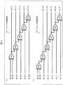
(動作の流れ例)
図5は、本発明の一実施形態に係るADC61の動作の流れの一例を示す図である。この図に示すように、ADC61は、入力されたグレイコードデータGC[1]〜GC[4]のいずれかとCNT信号53とのうち、基準クロックに対していずれか1つのみを遷移させる。言い換えると、上位ビットカウンタ部64は、CNT信号53の片方または両方のエッジを、基準クロックに対応して生成されるグレイコードデータ51に対応する複数の下位ビットと同時に遷移させない。これにより、グレイコードデータ51に対応する複数の下位ビットと、複数の上位ビットのうち最下位ビットとが、同じ基準クロックタイミングにおいて同時に遷移することを防ぐことができる。下位ビットラッチ部63は、比較器62の出力信号(VCO)が反転する時点で、グレイコードデータGC[1]〜GC[4]をラッチする。(Example of operation flow)
FIG. 5 is a diagram showing an example of an operation flow of the
ADC61は、CNT信号53と、比較器62の出力信号(VCO)に基づいて生成される信号FF_IN[5]とを、VCOが反転する時点でLow電位に固定させる。これにより、上位ビットカウンタ部64による上位ビットのカウントが停止する。
The
すべてのADC61によるデータが確定した後、ADC61は、下位ビットラッチ部63によってラッチされたグレイコードデータの各下位ビットをデータラッチ回路341〜345にラッチし、かつ、上位ビットカウンタ部64によってカウントされた最下位ビットを、ラッチ回路351にラッチする。
After the data of all the
反転制御信号54は、図5に示すビット第1反転タイミングでHigh電位からLow電位に遷移する。このタイミングでカウントされた上位ビットは、1の補数よりも1だけ少ないデータとなる。さらに、CNT信号53を、図5に示すビット第2反転タイミングでHigh電位からLow電位に遷移することによって、カウントされた上位ビットは1の補数(ビット反転データ)となる。本実施形態では、ビット第2反転タイミングにおけるCNT信号53の遷移を1回としており、かつ、ビット反転データは1の補数となっている。しかし、CNT信号53の遷移回数を変えることにより、ビット反転信号を1の補数+X(Xは−1以上の整数)とすることが可能である。また、ビット第2反転タイミングを、第2データのカウント終了後としてもよい。
The inversion control signal 54 transits from the High potential to the Low potential at the bit first inversion timing shown in FIG. The high-order bits counted at this timing are data that is one less than the one's complement. Further, by transitioning the
本実施形態では、ビット反転データを1の補数としており、ビットの反転後では、信号蓄積(状態変化)後の第2データをカウントした結果は、第1データよりも1だけ小さいものとなる。第2データにおける第1データからの絶対的な増加量を求めたい場合、CNT信号53の遷移回数を2回とすることによって、ビット反転データを2の補数とすればよい。また、ある単位画素21の第2データにおける他の単位画素21の第2データと比べた相対的なデータ変化量を求めるだけであれば、CNT信号53をHigh電位からLow電位に遷移させる動作は必要ない。この場合の演算結果は、絶対的な増加量よりも2小さいものとなる。
In the present embodiment, the bit inversion data is a 1's complement, and after the bit inversion, the result of counting the second data after signal accumulation (state change) is smaller than the first data by one. When it is desired to obtain the absolute increase amount of the second data from the first data, the bit inversion data can be set to the two's complement by setting the number of transitions of the
固体撮像素子1は、信号蓄積後の第2データを処理する前に、カウンタ生成部5を初期化する。初期状態と同様に、比較器62の出力(VCO)が反転する時点で、下位ビットラッチ部63はグレイコードデータをラッチし、上位ビットカウンタ部64は上位ビットのカウントを停止する。
The solid-
その後、ADC61は、ラッチ回路311〜315によってラッチされたグレイコードデータを、GD_S[0]〜GD_S[4]として、水平信号線71およびセンサアンプ72を通して信号処理部8に転送する。ADC61は、さらに、ラッチ回路341〜345によってラッチされたグレイコードデータを、グレイコードデータGD_R[0]〜GD_R[4]として、水平信号線71およびセンサアンプ72を通して信号処理部8に転送する。ADC61は、さらに、ラッチ回路351によってラッチされたデータを、バイナリデータBD_R[5]として信号処理部8に送信する。ADC61は、さらに、リップルカウンタ321〜328によって生成されたデータを、バイナリデータBD_S[5]〜BD_S[12]として、信号処理部8に送信する。信号処理部8は、入力された各データを使用してバイナリデータを復元する。
Then, the
(グレイバイナリ変換回路の構成例)
図6は、信号処理部8に送信されたグレイコードデータをバイナリデータに復元するためのグレイバイナリ変換回路701および702の構成例を示す図である。図6の(a)は、初期状態の第1データを処理するためのグレイバイナリ変換回路701の構成例を示す。図6の(b)は、信号蓄積後の第2データを処理するためのグレイバイナリ変換回路702の構成例を示す。グレイバイナリ変換回路701および702は、信号処理部8に備えられる。(Structure example of gray binary conversion circuit)
FIG. 6 is a diagram showing a configuration example of gray-binary conversion circuits 701 and 702 for restoring the gray code data transmitted to the
図6の(a)に示すように、グレイバイナリ変換回路701は、入力されたバイナリデータBD_R[5]およびグレイコードデータGD_R[0]〜GD_R[4]に変換処理を施すことによって初期状態の第1データの下位ビットのバイナリデータBD_R[0]〜BD_R[4]を生成する。図6の(b)に示すように、グレイバイナリ変換回路701は、入力されたバイナリデータBD_R[5]、バイナリデータBD_S[5]、およびグレイコードデータGD_R[0]〜GD_R[4]に変換処理を施すことによって、信号蓄積後の第2データの下位ビットのバイナリデータBD_S[0]〜BD_S[4]を生成する。 As shown in (a) of FIG. 6, the gray binary conversion circuit 701 converts the input binary data BD_R[5] and the gray code data GD_R[0] to GD_R[4] into the initial state. Binary data BD_R[0] to BD_R[4] of the lower bits of the first data are generated. As shown in FIG. 6B, the gray binary conversion circuit 701 converts the input binary data BD_R[5], the binary data BD_S[5], and the gray code data GD_R[0] to GD_R[4]. By performing the process, the binary data BD_S[0] to BD_S[4] of the lower bits of the second data after the signal accumulation is generated.
信号処理部8は、生成された下位ビットのバイナリデータBD_S[0]〜BD_S[4]と、初期状態の第1データを信号蓄積後の第2データから減算処理した上位バイナリデータBD[5]_S〜BD[12]_Sとをビット結合することによって、結合データを生成する。さらに、信号処理部8は、減算処理されていない初期状態の第1データの下位ビットのバイナリデータBD_R[0]〜BD_R[4]を結合データから減算することによって、信号蓄積後の第2データから初期状態の第1データを減算した値に上位ビットの最下位ビットが1だけ少ない値を得ることができる。信号処理部8において絶対値の補正処理が行われることが多く、他の単位画素21との相対的な差を求められれば十分なことが多い。なお、減算値の上位ビットの最下位ビットに1を加算すれば、絶対的な増加量を算出することができる。U/DカウンタにおいてCNT信号53をHigh電位からLow電位に遷移させることによって1を加算した場合、信号処理部8において上位ビットの最下位ビットに1を加算する必要はない。
The
本実施形態に係るADC61は、下位ビットラッチ部63によってキャリー信号を生成するのではなく、下位ビットラッチ部63に送信されるデータとは別に、上位ビットカウンタ部64による上位ビットのカウントに必要な制御信号(CNT信号53)を、上位ビットカウンタ部64に送信する。これによりADC61は、下位ビットの複数のビットと上位ビットの最下位ビットの変化時点とを、ビットの不整合が起こらない時点に制御することができる。そのため、ADC61の回路構成および設計を簡素化することができる。
The
〔まとめ〕
本発明の態様1に係るアナログデジタル変換器は、少なくとも1つの列または少なくとも1つの単位画素ごとに配置され、入力されたアナログ信号をデジタル信号に変換するアナログデジタル変換器であって、前記アナログ信号の電圧と、基準クロックに対応して電圧値が変化する参照電圧とを比較する比較器と、前記比較器の出力が反転したことをトリガとして、前記基準クロックに対応したグレイコードデータを下位ビットとしてラッチする下位ビットラッチ部と、前記基準クロックに対応した制御信号の片方または両方のエッジをカウントし、かつ、前記比較器の出力が反転したことをトリガとして、上位ビットのカウントを停止する上位ビットカウンタ部とを備えていることを特徴としている。[Summary]
An analog-digital converter according to a first aspect of the present invention is an analog-digital converter that is arranged for at least one column or at least one unit pixel and converts an input analog signal into a digital signal. Of the gray code data corresponding to the reference clock is triggered by the inversion of the output of the comparator and a comparator that compares the voltage of the reference voltage with a reference voltage whose voltage value changes corresponding to the reference clock. And a lower bit latch unit that counts one or both edges of the control signal corresponding to the reference clock and stops the counting of the upper bit triggered by the inversion of the output of the comparator. It is characterized by including a bit counter section.
前記の構成によれば、マスク信号を生成することなくビットの非整合性を防止することができるので、アナログデジタル変換器の回路構成および設計を簡素化することができる。 According to the above configuration, it is possible to prevent bit inconsistency without generating a mask signal, and therefore it is possible to simplify the circuit configuration and design of the analog-digital converter.
本発明の態様2に係るアナログデジタル変換器は、前記態様1において、前記上位ビットカウンタ部は、前記制御信号の片方または両方のエッジを、前記基準クロックに対応して生成される前記グレイコードデータに対応する複数の前記下位ビットと同時に遷移させないことを特徴としている。
In the analog-digital converter according to
前記の構成によれば、グレイコードデータに対応する複数の下位ビットと、複数の上位ビットのうち最下位ビットとが、同じ基準クロックタイミングにおいて同時に遷移することを防ぐことができる。 According to the above configuration, it is possible to prevent the plurality of lower bits corresponding to the gray code data and the least significant bit of the plurality of upper bits from simultaneously transiting at the same reference clock timing.
本発明の態様3に係るアナログデジタル変換器は、前記態様1において、前記上位ビットカウンタ部は、縦続接続された複数のリップルカウンタを有し、前記アナログ信号は、初期状態の第1データと、信号蓄積後の第2データとを含み、それぞれの前記リップルカウンタは、前記制御信号に基づいて、前記第1データのカウントが終了された後から前記第2データのカウントが開始される前の任意の時点で反転制御信号およびCNT信号によって1の補数+X(Xは−1以上の整数)にビット反転し、かつ、前記第1データに対応する複数の前記上位ビットのうち最下位ビットを前記制御信号に基づいて任意の時点でラッチすることを特徴としている。CNT信号は、下位ビットのラッチ部と独立しているため、CNT信号を独立で遷移させることが可能となる。さらに、アナログデジタル変換器の回路構成を変更することなく、反転データを1の補数+X(Xは−1以上の整数)としたデータとすることが可能である。 An analog-digital converter according to a third aspect of the present invention is the analog-digital converter according to the first aspect, wherein the higher-order bit counter section has a plurality of cascade-connected ripple counters, and the analog signal is first data in an initial state, 2nd data after signal accumulation, and each of the ripple counters is optional based on the control signal after the count of the first data is ended and before the count of the second data is started. Bit inversion to 1's complement +X (X is an integer greater than or equal to -1) by the inversion control signal and the CNT signal, and controlling the least significant bit of the plurality of upper bits corresponding to the first data. It is characterized in that it is latched at any time based on a signal. Since the CNT signal is independent of the lower bit latch unit, the CNT signal can be independently transitioned. Furthermore, it is possible to make the inverted data into data of 1's complement +X (X is an integer of -1 or more) without changing the circuit configuration of the analog-digital converter.
前記の構成によれば、アップダウンにより不明となる上位ビットの最下位ビットの値を保存可能となり、かつ、下位ビットの情報と合わせて、正確にバイナリデータに復元することが可能である。また、反転データは、アナログデジタル変換器の回路構成を変更することなく1の補数+X(Xは−1以上の整数)の範囲で可変であり、用途に応じてアナログデジタル変換器の仕様を容易に変更可能である。 According to the above configuration, it is possible to store the value of the least significant bit of the upper bits that becomes unknown due to up/down, and it is possible to accurately restore binary data together with the information of the lower bits. In addition, the inverted data can be changed within the range of 1's complement + X (X is an integer greater than -1) without changing the circuit configuration of the analog-digital converter, and the specifications of the analog-digital converter can be easily adjusted according to the application. Can be changed to.
本発明の態様4に係るアナログデジタル変換器は、前記態様3において、水平信号線と、転送されたデータを信号処理する信号処理部とをさらに備えており、前記下位ビットラッチ部は、前記第1データに対応する下位ビットを、前記水平信号線を通じて前記信号処理部に転送し、前記上位ビットカウンタ部は、ラッチされた前記第1データのカウントが終了する時点における前記第1データに対応する複数の前記上位ビットのうち最下位ビットを、前記水平信号線を通じて前記信号処理部に転送し、前記信号処理部は、前記第1データに対応する前記下位ビットのバイナリデータを復元することを特徴としている。 An analog-digital converter according to a fourth aspect of the present invention is the analog-to-digital converter according to the third aspect, further comprising a horizontal signal line and a signal processing unit that processes the transferred data. The lower bit corresponding to one data is transferred to the signal processing unit through the horizontal signal line, and the upper bit counter unit corresponds to the first data at the time when the counting of the latched first data ends. The least significant bit of the plurality of upper bits is transferred to the signal processing unit through the horizontal signal line, and the signal processing unit restores the binary data of the lower bit corresponding to the first data. I am trying.
前記の構成によれば、下位ビットのバイナリデータを復元することができる。 According to the above configuration, the lower-order bit binary data can be restored.
本発明の態様5に係るアナログデジタル変換器は、前記態様3において、水平信号線と、転送したデータを信号処理する信号処理部とをさらに備えており、前記下位ビットラッチ部は、前記第2データに対応する前記下位ビットを前記水平信号線を通じて前記信号処理部に転送し、前記上位ビットカウンタ部は、ラッチされた前記第1データのカウントが終了する時点における前記第1データに対応する複数の前記上位ビットのうち最下位ビットと、前記第2データのカウントが終了する時点における前記第1データに対応する複数の前記上位ビットのうち最下位ビットとを、前記水平信号線を通じて前記信号処理部に転送し、前記信号処理部は、前記第2データに対応する前記下位ビットのバイナリデータを復元することを特徴としている。 An analog-digital converter according to a fifth aspect of the present invention is the analog-digital converter according to the third aspect, further including a horizontal signal line and a signal processing unit that performs signal processing on the transferred data. The lower bit corresponding to the data is transferred to the signal processing unit through the horizontal signal line, and the upper bit counter unit corresponds to the first data at the time when the counting of the latched first data ends. The least significant bit of the upper bits and the least significant bit of the plurality of upper bits corresponding to the first data at the time when the counting of the second data ends, through the horizontal signal line. And the signal processing unit restores the binary data of the lower bit corresponding to the second data.
前記の構成によれば、下位ビットのバイナリデータを正確に復元することができる。 According to the above configuration, the lower-order bit binary data can be accurately restored.
本発明の態様6に係るアナログデジタル変換器は、前記態様4または5において、前記信号処理部は、前記バイナリデータに復元された前記第2データに対応する前記下位ビットと、前記第2データのカウントが終了された後の前記上位ビットとをビット結合した結合データから、前記バイナリデータに復元された前記第1データに対応する前記下位ビットを減算し、前記第2データにおける前記第1データからのデータの増加量を算出することを特徴としている。
An analog-digital converter according to
前記の構成によれば、データの増加量を正確に算出することができる。 According to the above configuration, it is possible to accurately calculate the increase amount of data.
本発明の態様7に係る固体撮像素子 は、入射光をアナログ信号に変換する画素部と、前記アナログ信号をデジタル信号に変換する態様1〜6のいずれかのアナログデジタル変換器と、前記アナログ信号を前記画素部から前記アナログデジタル変換器に転送するための垂直信号線とを備えていることを特徴としている。
A solid-state imaging device according to
前記の構成によれば、マスク信号を生成することなくビットの非整合性を防止することができる固体撮像素子を提供することができる。 According to the above configuration, it is possible to provide a solid-state image sensor capable of preventing bit inconsistency without generating a mask signal.
本発明は前述した各実施形態に限定されるものではなく、請求項に示した範囲で種々の変更が可能である。異なる実施形態にそれぞれ開示された技術的手段を適宜組み合わせて得られる実施形態も、本発明の技術的範囲に含まれる。各実施形態にそれぞれ開示された技術的手段を組み合わせることによって、新しい技術的特徴を形成することもできる。 The present invention is not limited to the embodiments described above, and various modifications can be made within the scope of the claims. Embodiments obtained by appropriately combining the technical means disclosed in the different embodiments are also included in the technical scope of the present invention. A new technical feature can be formed by combining the technical means disclosed in each embodiment.
1 固体撮像素子、2 画素部、3 行選択回路、4 参照電圧生成部、5 カウンタ生成部、6 ADC部、7 列選択回路、8 信号処理部、21 単位画素、22 垂直信号線、51 グレイコードデータ、53 CNT信号、54 反転制御信号、61 ADC(アナログデジタル変換器)、62 比較器、63 下位ビットラッチ部、64 上位ビットカウンタ部、71 水平信号線、72 センサアンプ 1 solid-state imaging device, 2 pixel unit, 3 row selection circuit, 4 reference voltage generation unit, 5 counter generation unit, 6 ADC unit, 7 column selection circuit, 8 signal processing unit, 21 unit pixel, 22 vertical signal line, 51 gray Code data, 53 CNT signal, 54 inversion control signal, 61 ADC (analog-digital converter), 62 comparator, 63 lower bit latch section, 64 upper bit counter section, 71 horizontal signal line, 72 sensor amplifier
Claims (7)
前記アナログ信号の電圧と、基準クロックに対応して電圧値が変化する参照電圧とを比較する比較器と、
前記比較器の出力が反転したことをトリガとして、前記基準クロックに対応したグレイコードデータを下位ビットとしてラッチする下位ビットラッチ部と、
前記基準クロックに対応した制御信号の片方または両方のエッジをカウントし、かつ、前記比較器の出力が反転したことをトリガとして、上位ビットのカウントを停止する上位ビットカウンタ部とを備えていることを特徴とするアナログデジタル変換器。An analog-digital converter which is arranged for at least one column or at least one unit pixel and which converts an input analog signal into a digital signal,
A comparator for comparing the voltage of the analog signal with a reference voltage whose voltage value changes corresponding to a reference clock;
A lower bit latch unit that latches the gray code data corresponding to the reference clock as a lower bit, triggered by the inversion of the output of the comparator,
An upper bit counter unit that counts one or both edges of the control signal corresponding to the reference clock and that stops the counting of the upper bits by using the inversion of the output of the comparator as a trigger. An analog-digital converter characterized by.
前記アナログ信号は、初期状態の第1データと、信号蓄積後の第2データとを含み、
それぞれの前記リップルカウンタは、前記制御信号に基づいて、前記第1データのカウントが終了された後から前記第2データのカウントが開始される前の任意の時点で反転制御信号およびCNT信号によって1の補数+X(Xは−1以上の整数)にビット反転し、かつ、前記第1データに対応する複数の前記上位ビットのうち最下位ビットを前記制御信号に基づいて任意の時点でラッチすることを特徴とする請求項1に記載のアナログデジタル変換器。The high-order bit counter unit has a plurality of ripple counters that are cascaded,
The analog signal includes first data in an initial state and second data after signal accumulation,
Each of the ripple counters is set to 1 by an inversion control signal and a CNT signal based on the control signal at an arbitrary time point after the counting of the first data is ended and before the counting of the second data is started. Complement +X (X is an integer equal to or greater than -1) and latch the least significant bit of the plurality of upper bits corresponding to the first data at any time based on the control signal. The analog-digital converter according to claim 1, characterized in that.
前記下位ビットラッチ部は、前記第1データに対応する下位ビットを、前記水平信号線を通じて前記信号処理部に転送し、
前記上位ビットカウンタ部は、ラッチされた前記第1データのカウントが終了する時点における前記第1データに対応する複数の前記上位ビットのうち最下位ビットを、前記水平信号線を通じて前記信号処理部に転送し、
前記信号処理部は、前記第1データに対応する前記下位ビットのバイナリデータを復元することを特徴とする請求項3に記載のアナログデジタル変換器。Further comprising a horizontal signal line and a signal processing unit that processes the transferred data,
The lower bit latch unit transfers a lower bit corresponding to the first data to the signal processing unit through the horizontal signal line,
The upper bit counter unit transfers the least significant bit of the plurality of upper bits corresponding to the first data to the signal processing unit through the horizontal signal line when the counting of the latched first data ends. Transfer,
The analog-digital converter according to claim 3, wherein the signal processing unit restores the lower-order binary data corresponding to the first data.
前記下位ビットラッチ部は、前記第2データに対応する前記下位ビットを前記水平信号線を通じて前記信号処理部に転送し、
前記上位ビットカウンタ部は、ラッチされた前記第1データのカウントが終了する時点における前記第1データに対応する複数の前記上位ビットのうち最下位ビットと、前記第2データのカウントが終了する時点における前記第1データに対応する複数の前記上位ビットのうち最下位ビットとを、前記水平信号線を通じて前記信号処理部に転送し、
前記信号処理部は、前記第2データに対応する前記下位ビットのバイナリデータを復元することを特徴とする請求項3に記載のアナログデジタル変換器。It further comprises a horizontal signal line and a signal processing unit for processing the transferred data,
The lower bit latch unit transfers the lower bit corresponding to the second data to the signal processing unit through the horizontal signal line,
The high-order bit counter unit is configured to count the least significant bit of the plurality of high-order bits corresponding to the first data at the time when the counting of the latched first data ends and the time when the counting of the second data ends. Transferring the least significant bit of the plurality of upper bits corresponding to the first data to the signal processing unit through the horizontal signal line,
The analog-digital converter according to claim 3, wherein the signal processing unit restores the lower-order binary data corresponding to the second data.
前記アナログ信号をデジタル信号に変換する請求項1〜6のいずれか1項に記載のアナログデジタル変換器と、
前記アナログ信号を前記画素部から前記アナログデジタル変換器に転送するための垂直信号線とを備えていることを特徴とする固体撮像素子。A pixel unit that converts incident light into an analog signal,
The analog-digital converter according to any one of claims 1 to 6, which converts the analog signal into a digital signal,
And a vertical signal line for transferring the analog signal from the pixel unit to the analog-digital converter.
Applications Claiming Priority (3)
| Application Number | Priority Date | Filing Date | Title |
|---|---|---|---|
| JP2017120418 | 2017-06-20 | ||
| JP2017120418 | 2017-06-20 | ||
| PCT/JP2018/022106 WO2018235638A1 (en) | 2017-06-20 | 2018-06-08 | Analog-digital converter and solid-state imaging device |
Publications (2)
| Publication Number | Publication Date |
|---|---|
| JPWO2018235638A1 JPWO2018235638A1 (en) | 2020-03-19 |
| JP6726362B2 true JP6726362B2 (en) | 2020-07-22 |
Family
ID=64735949
Family Applications (1)
| Application Number | Title | Priority Date | Filing Date |
|---|---|---|---|
| JP2019525394A Active JP6726362B2 (en) | 2017-06-20 | 2018-06-08 | Analog-digital converter and solid-state image sensor |
Country Status (3)
| Country | Link |
|---|---|
| US (1) | US11133822B2 (en) |
| JP (1) | JP6726362B2 (en) |
| WO (1) | WO2018235638A1 (en) |
Family Cites Families (13)
| Publication number | Priority date | Publication date | Assignee | Title |
|---|---|---|---|---|
| US7671317B2 (en) * | 2007-07-25 | 2010-03-02 | Panasonic Corporation | Physical quantity detecting apparatus and method for driving the same |
| JP5347341B2 (en) * | 2008-06-06 | 2013-11-20 | ソニー株式会社 | Solid-state imaging device, imaging device, electronic device, AD conversion device, AD conversion method |
| JP5375277B2 (en) * | 2009-04-02 | 2013-12-25 | ソニー株式会社 | Solid-state imaging device, imaging device, electronic device, AD conversion device, AD conversion method |
| JP5728826B2 (en) | 2010-04-30 | 2015-06-03 | ソニー株式会社 | Column A / D converter, column A / D conversion method, solid-state imaging device, and camera system |
| JP5799531B2 (en) * | 2010-04-30 | 2015-10-28 | ソニー株式会社 | A / D converter, A / D conversion method, solid-state imaging device, and camera system |
| JP5528204B2 (en) * | 2010-05-14 | 2014-06-25 | パナソニック株式会社 | Solid-state imaging device, imaging system, and driving method of solid-state imaging device |
| US9357147B2 (en) * | 2012-02-29 | 2016-05-31 | Sony Corporation | Column A/D converter, column A/D conversion method, solid imaging device, and camera system |
| KR102135684B1 (en) * | 2013-07-24 | 2020-07-20 | 삼성전자주식회사 | Counter circuit, ADC and Image sensor incluing the same and method of correlated double sampling |
| JP2015037206A (en) * | 2013-08-12 | 2015-02-23 | キヤノン株式会社 | Imaging apparatus |
| KR102292644B1 (en) * | 2013-12-24 | 2021-08-23 | 삼성전자주식회사 | Image sensor for operating with high speed |
| JP6314477B2 (en) * | 2013-12-26 | 2018-04-25 | ソニー株式会社 | Electronic devices |
| JP2016213549A (en) * | 2015-04-30 | 2016-12-15 | 国立大学法人北海道大学 | Digital circuit and analog/digital (a/d) conversion circuit and digital signal processing method |
| JP6753985B2 (en) * | 2018-08-10 | 2020-09-09 | シャープ株式会社 | Analog-to-digital converter and solid-state image sensor |
-
2018
- 2018-06-08 US US16/625,669 patent/US11133822B2/en active Active
- 2018-06-08 WO PCT/JP2018/022106 patent/WO2018235638A1/en active Application Filing
- 2018-06-08 JP JP2019525394A patent/JP6726362B2/en active Active
Also Published As
| Publication number | Publication date |
|---|---|
| US20210135682A1 (en) | 2021-05-06 |
| WO2018235638A1 (en) | 2018-12-27 |
| US11133822B2 (en) | 2021-09-28 |
| JPWO2018235638A1 (en) | 2020-03-19 |
Similar Documents
| Publication | Publication Date | Title |
|---|---|---|
| US8749420B2 (en) | A/D converter, A/D conversion method, and program | |
| JP4744343B2 (en) | Solid-state imaging device and driving method of solid-state imaging device | |
| US10340936B2 (en) | Analog-to-digital conversion and method of analog-to-digital conversion | |
| US10348323B2 (en) | Analog-to-digital conversion and method of analog-to-digital conversion | |
| JP4661891B2 (en) | AD converter, solid-state imaging device, and camera system | |
| JP5799531B2 (en) | A / D converter, A / D conversion method, solid-state imaging device, and camera system | |
| JP6674224B2 (en) | Solid-state imaging device | |
| JP6019793B2 (en) | COUNTER, COUNTING METHOD, AD CONVERTER, SOLID-STATE IMAGING ELEMENT, AND ELECTRONIC DEVICE | |
| JP2011234326A (en) | Column a/d converter, column a/d conversion method, solid state imaging device and camera system | |
| JP2009225324A (en) | A/d converter, a/d conversion method, solid-state image pickup element, and camera system | |
| JP6124016B2 (en) | AD conversion apparatus and AD conversion method | |
| JP6753985B2 (en) | Analog-to-digital converter and solid-state image sensor | |
| JPWO2009131018A1 (en) | A / D converter for image sensor | |
| JP5507309B2 (en) | Signal processing method and solid-state imaging device | |
| JP6726362B2 (en) | Analog-digital converter and solid-state image sensor | |
| JP2016184893A (en) | Binary value conversion circuit and method, ad converter and solid state image sensor | |
| JP2017005332A (en) | Cyclic ad converter, digital corrector for cyclic ad converter, and method thereof | |
| JP2016213531A (en) | AD converter and AD conversion method | |
| CN113225085A (en) | High-speed one-step multi-bit successive approximation-pipeline hybrid analog-digital converter | |
| Baek et al. | Design of a 10-bit CMOS image sensor based on an 8-bit configurable hold-and-go counter | |
| JP2011259219A (en) | Pipeline ad converter circuit | |
| JP5129298B2 (en) | DWA (Data-Weighted-Averaging) circuit and delta-sigma modulator using the same | |
| KR102170958B1 (en) | Analog to Digital Converter Using Logical Shift Counter | |
| KR20230099899A (en) | Count using milti clock and method performing thereof | |
| JP2011071966A (en) | Pipelined analog/digital conversion apparatus |
Legal Events
| Date | Code | Title | Description |
|---|---|---|---|
| A621 | Written request for application examination |
Free format text: JAPANESE INTERMEDIATE CODE: A621 Effective date: 20191118 |
|
| TRDD | Decision of grant or rejection written | ||
| A01 | Written decision to grant a patent or to grant a registration (utility model) |
Free format text: JAPANESE INTERMEDIATE CODE: A01 Effective date: 20200602 |
|
| A61 | First payment of annual fees (during grant procedure) |
Free format text: JAPANESE INTERMEDIATE CODE: A61 Effective date: 20200626 |
|
| R150 | Certificate of patent or registration of utility model |
Ref document number: 6726362 Country of ref document: JP Free format text: JAPANESE INTERMEDIATE CODE: R150 |