JP6723736B2 - Imaging device, imaging system, and method of driving imaging device - Google Patents
Imaging device, imaging system, and method of driving imaging device Download PDFInfo
- Publication number
- JP6723736B2 JP6723736B2 JP2015241382A JP2015241382A JP6723736B2 JP 6723736 B2 JP6723736 B2 JP 6723736B2 JP 2015241382 A JP2015241382 A JP 2015241382A JP 2015241382 A JP2015241382 A JP 2015241382A JP 6723736 B2 JP6723736 B2 JP 6723736B2
- Authority
- JP
- Japan
- Prior art keywords
- signal
- pixel
- capacitive element
- holding unit
- image pickup
- Prior art date
- Legal status (The legal status is an assumption and is not a legal conclusion. Google has not performed a legal analysis and makes no representation as to the accuracy of the status listed.)
- Active
Links
Images


Classifications
-
- H—ELECTRICITY
- H04—ELECTRIC COMMUNICATION TECHNIQUE
- H04N—PICTORIAL COMMUNICATION, e.g. TELEVISION
- H04N25/00—Circuitry of solid-state image sensors [SSIS]; Control thereof
- H04N25/70—SSIS architectures; Circuits associated therewith
- H04N25/76—Addressed sensors, e.g. MOS or CMOS sensors
- H04N25/77—Pixel circuitry, e.g. memories, A/D converters, pixel amplifiers, shared circuits or shared components
- H04N25/772—Pixel circuitry, e.g. memories, A/D converters, pixel amplifiers, shared circuits or shared components comprising A/D, V/T, V/F, I/T or I/F converters
-
- H—ELECTRICITY
- H04—ELECTRIC COMMUNICATION TECHNIQUE
- H04N—PICTORIAL COMMUNICATION, e.g. TELEVISION
- H04N25/00—Circuitry of solid-state image sensors [SSIS]; Control thereof
- H04N25/70—SSIS architectures; Circuits associated therewith
- H04N25/71—Charge-coupled device [CCD] sensors; Charge-transfer registers specially adapted for CCD sensors
- H04N25/75—Circuitry for providing, modifying or processing image signals from the pixel array
Description
本発明は、撮像装置、撮像システム、撮像装置の駆動方法に関する。 The present invention relates to an imaging device, an imaging system, and a driving method of the imaging device.
複数行、複数列に渡って複数の画素が配された撮像装置が知られている。 There is known an imaging device in which a plurality of pixels are arranged in a plurality of rows and a plurality of columns.
さらに特許文献1のように、画素が出力する信号を保持する信号保持部と、信号保持部に保持された信号をデジタル信号に変換するAD変換部とを有する撮像装置がある。信号保持部と画素との間の電気的経路にはスイッチが設けられている。このスイッチが導通した後、非導通となることによって、信号保持部は、画素の出力する信号を保持する。
Further, there is an imaging device having a signal holding unit that holds a signal output from a pixel and an AD conversion unit that converts the signal held in the signal holding unit into a digital signal, as in
特許文献1の撮像装置では、スイッチが導通、非導通の動作を行うことによって生じるノイズが、画素が出力する信号に重畳される。このため、信号保持部が保持する信号に含まれるノイズが増加する課題があった。
In the image pickup device of
本発明は上記の課題を鑑みて為されたものであり、一の態様は、画素信号を各々が出力する複数の画素と、前記複数の画素の各々から前記画素信号が出力される信号線と、容量素子と、信号保持部と、一方のノードが前記信号線に接続され、他方のノードが前記容量素子と前記信号保持部に接続されたスイッチとを有し、前記容量素子は、前記スイッチがオンしている場合には、前記信号線に出力されている前記画素信号をサンプリングし、前記スイッチがオンからオフした場合には前記信号線に出力されている前記画素信号を保持する素子であって、前記複数の画素のうちの第1の画素の前記画素信号が前記信号線に出力され、前記スイッチをオンすることによって前記容量素子がサンプリングしている前記第1の画素の画素信号に基づく信号が、前記スイッチをオンしたまま、前記信号保持部に保持されることを特徴とする撮像装置である。 The present invention has been made in view of the above problems, and one aspect is a plurality of pixels each outputting a pixel signal, and a signal line from which the pixel signal is output from each of the plurality of pixels. A capacitive element, a signal holding unit, and a switch having one node connected to the signal line and the other node connected to the capacitive element and the signal holding unit , wherein the capacitive element is the switch When the switch is on, the pixel signal output to the signal line is sampled, and when the switch is turned off, the pixel signal output to the signal line is held by the element. Then, the pixel signal of the first pixel of the plurality of pixels is output to the signal line, and when the switch is turned on, the pixel signal of the first pixel is sampled by the capacitive element. In the image pickup apparatus, a signal based on the signal is held in the signal holding unit while the switch is turned on.
また、別の一の態様は、画素信号を各々が出力する複数の画素と、前記複数の画素の各々から前記画素信号が出力される信号線と、容量素子と、前記画素信号に基づく信号を保持する信号保持部とを有し、前記容量素子が、前記画素信号のサンプリングと、前記画素信号の保持とが可能な素子である撮像装置の駆動方法であって、前記複数の画素のうちの第1の画素が前記画素信号を前記信号線に出力し、前記容量素子が前記第1の画素の画素信号をサンプリングしている期間に、前記第1の画素の画素信号に基づく信号を、前記信号保持部が保持することを特徴とする撮像装置の駆動方法である。 Another aspect is to provide a plurality of pixels each outputting a pixel signal, a signal line from which the pixel signal is output from each of the plurality of pixels, a capacitive element, and a signal based on the pixel signal. A driving method of an image pickup apparatus, comprising: a signal holding unit for holding, wherein the capacitive element is an element capable of sampling the pixel signal and holding the pixel signal, A signal based on the pixel signal of the first pixel is output during a period in which the first pixel outputs the pixel signal to the signal line and the capacitive element is sampling the pixel signal of the first pixel. A method of driving an image pickup apparatus, characterized in that the signal holding unit holds the signal.
本発明により、信号保持部が保持する信号のノイズを低減させることができる。 According to the present invention, the noise of the signal held by the signal holding unit can be reduced.
以下、図面を参照しながら、各実施例を説明する。 Hereinafter, each embodiment will be described with reference to the drawings.
(実施例1)
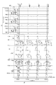
図1は、本実施例の撮像装置の構成を示した図である。撮像装置は、画素アレイ1000、増幅回路1100、サンプルホールド部1200、AD変換部1300を有する。さらに撮像装置は、電流源160、垂直走査回路170、カウンタ320、水平走査回路360を有する。
(Example 1)
FIG. 1 is a diagram showing the configuration of the image pickup apparatus of this embodiment. The imaging device has a
画素アレイ1000は、複数行および複数列に渡って配された画素150を有する。画素150は、フォトダイオード10p、リセットトランジスタ11p、選択トランジスタ12p、増幅トランジスタ13p、転送トランジスタ14pを有する。なお、pには、画素が位置する行の番号から1を引いた数が入る。フォトダイオード10pは、光に基づく電荷を生成する光電変換部である。転送トランジスタ14p、フォトダイオード10pと、増幅トランジスタ13pの入力ノードに接続されている。また、転送トランジスタ14pのゲートには、垂直走査回路170から信号READ(n)が入力される。なお、(n)は、垂直走査回路170が出力する信号について、n行目の画素150に入力されることを示す。リセットトランジスタ11pは、一方のノードは増幅トランジスタ13pの入力ノードに接続され、他方のノードは、電源電圧が入力される。リセットトランジスタ11pのゲートには、垂直走査回路170から、信号RES(n)が入力される。増幅トランジスタ13pの一方のノードは、選択トランジスタ12pに接続され、他方のノードには電源電圧が入力される。選択トランジスタ12pの一方のノードは増幅トランジスタ13pに接続され、他方のノードは垂直信号線165に接続される。選択トランジスタ12pのゲートには、垂直走査回路170から信号SEL(n)が入力される。垂直信号線165は、電流源160と、増幅回路1100が有するスイッチ175に接続される。信号PSEL(n)がHighとなると、選択トランジスタ12pがオンする。これにより、電流源160が供給する電流が、選択トランジスタ12pを介して、増幅トランジスタ13pに入力される。増幅トランジスタ13pは、入力ノードの電位に基づく信号である画素信号を、選択トランジスタ12pを介して垂直信号線165に出力する。増幅トランジスタ13pは、電源電圧、電流源160によってソースフォロワ動作を行う。別の言い方をすれば、電源電圧、電流源160、増幅トランジスタ13pは、ソースフォロワ回路を構成する。
The
増幅回路1100は、スイッチ175、容量素子190、アンプ180、容量素子200、スイッチ210を有する。スイッチ175は、不図示のタイミングジェネレータから入力される信号VLONによって制御される。また、スイッチ210は、不図示のタイミングジェネレータから入力される信号ARESによって制御される。アンプ180は、入力される信号を、容量素子190の容量値/容量素子200の容量値で表されるゲインで増幅した信号を、サンプルホールド部1200が有するスイッチ220に出力する。
The amplifier circuit 1100 includes a
サンプルホールド部1200は、スイッチ220、容量素子230、バッファ240、スイッチ250を有する。スイッチ220は、不図示のタイミングジェネレータから入力される信号SHによって制御される。スイッチ250は、不図示のタイミングジェネレータから入力される信号THによって制御される。容量素子230は、スイッチ220が導通した後、非導通となることによって、画素150が出力する信号に基づく信号を保持する容量素子である。容量素子230は、一方のノードがスイッチ220に接続されている。また、容量素子230の一方のノードは、バッファ240、容量素子260、比較器280、ラッチ310を介して、信号保持部である第1メモリ330に接続されている。容量素子230の他方のノードには、基準電圧である、接地電圧が入力される。バッファ240は、入力された信号をバッファリングして、AD変換部1300が有する容量素子260に出力する。増幅回路1100の出力は、出力V_AOUT(m)と表す。(m)は、m列目の増幅回路1100であることを示している。
The
AD変換部1300は、容量素子260、容量素子270、比較器280、スイッチ290、スイッチ300、ラッチ310、第1メモリ330、スイッチ340、第2メモリ350を有する。
The
比較器280の一方の入力ノードは、容量素子260に接続されている。比較器280の他方の入力ノードは、容量素子270を有する。容量素子270には、不図示のランプ信号供給部から、ランプ信号RAMPが入力される。スイッチ290、スイッチ300は、それぞれ、不図示のタイミングジェネレータから出力される信号CRESによって制御される。ラッチ310には、比較器280の出力V_COUNT(m)が入力される。(m)は、m列目の比較器280が出力する信号であることを示している。ラッチ310は、比較器280の出力V_COUT(m)を受けて、LAT(m)を第1メモリ330に出力する。
One input node of the
カウンタ320は、クロック信号を計数することによってカウント信号を生成する。第1メモリ330には、カウンタ320が出力するカウント信号が入力される。
The
スイッチ340は不図示のタイミングジェネレータから入力される信号MREADによって制御される。スイッチ340がオンすると、第2メモリ350は、第1メモリが保持した信号を保持する。
The
水平走査回路360は、各列の第2メモリ350を順次走査することによって、各列の第2メモリ350から、当該第2メモリ350が保持した信号を出力部370に読み出す。
The
出力部370は、第2メモリ350から出力された信号を、撮像装置の外部に出力する。
The
次に、図1の撮像装置の構成を用いた、比較例の動作を説明する。 Next, the operation of the comparative example using the configuration of the image pickup apparatus in FIG. 1 will be described.
図2(a)は、比較例の動作を示した図である。図2(a)に示した動作では、NAD期間とS読み期間とが重なっている。また、SAD期間と次行の画素150のN読み期間とが重なっている。
FIG. 2A is a diagram showing the operation of the comparative example. In the operation shown in FIG. 2A, the NAD period and the S reading period overlap. In addition, the SAD period and the N reading period of the
図2(a)に示した動作の詳細の動作を図3に示す。 The detailed operation of the operation shown in FIG. 2A is shown in FIG.
図3に示す時刻t0から時刻t8までの期間が、図2(a)に示したN読み期間である。 The period from time t0 to time t8 shown in FIG. 3 is the N reading period shown in FIG.
図3の時刻t0に、垂直走査回路170は、信号SEL(1)をHighにする。これにより、1行目の画素150から信号が垂直信号線165に出力される。
At time t0 in FIG. 3, the
図3の時刻t1に、垂直走査回路170は、信号RES(1)をHighからLowにする。これにより、増幅トランジスタ13pの入力ノードは、リセット後の電位となっている。これにより、1行目の画素150の増幅トランジスタ130は、リセットされた入力ノードの電位に基づく信号を、垂直信号線165に出力する。この信号をN信号と表記する。N信号は、画素150が出力する画素信号の1つであり、画素150が出力するノイズ信号である。
At time t1 in FIG. 3, the
画素150がN信号を出力している期間である時刻t2に、不図示のタイミングジェネレータは、信号ARESをHighからLowに遷移させる。これにより、容量素子190には、N信号がクランプされる。
At time t2, which is the period during which the
時刻t2から、増幅回路1100は、オフセットレベルの信号であるOFFSET信号を出力する。この信号をオフセット信号と表記する。このOFFSET信号は、画素信号の一つであるノイズ信号に基づく信号である。不図示のタイミングジェネレータが、信号SHをHighとしているので、容量素子230はOFFSET信号をサンプリングする。
From time t2, the amplifier circuit 1100 outputs the OFFSET signal which is the signal of the offset level. This signal is referred to as an offset signal. The OFFSET signal is a signal based on a noise signal which is one of pixel signals. Since the timing generator (not shown) sets the signal SH to High, the
その後、時刻t3に、不図示のタイミングジェネレータは、信号SHをLowにする。これにより、容量素子230は、OFFSET信号を保持する。
After that, at time t3, the timing generator (not shown) sets the signal SH to Low. As a result, the
バッファ240には、容量素子230が保持したOFFSET信号が入力される。バッファ240は、このOFFSET信号をバッファリングした信号を、容量素子260を介して比較器280に出力する。
The OFFSET signal held by the
この時、ランプ信号RAMPの電位は、ランプ開始電位に設定されている。 At this time, the potential of the ramp signal RAMP is set to the ramp start potential.
その後、時刻t3から時刻t4に、ランプ信号供給部はランプ信号RAMPの電位をオフセットさせる。 Then, from time t3 to time t4, the ramp signal supply unit offsets the potential of the ramp signal RAMP.
時刻t6に、不図示のタイミングジェネレータは、信号CRESをHighからLowに変化させる。容量素子260は、OFFSET信号をクランプする。また、容量素子270は、ランプ信号RAMPのオフセットされた電位をクランプする。
At time t6, a timing generator (not shown) changes the signal CRES from High to Low. The
N読み期間は、画素150がN信号の出力を開始してから、後述する、ランプ信号RAMPが電位の変化を開始するまでの期間である。
The N reading period is a period from when the
次に、NAD期間を説明する。 Next, the NAD period will be described.
時刻t8では、不図示のランプ信号供給部は、ランプ信号RAMPの電位を、ランプ開始電位に設定している。そして、時刻t8に、ランプ信号供給部は、ランプ信号RAMPの電位の変化を開始する。 At time t8, the ramp signal supply unit (not shown) sets the potential of the ramp signal RAMP to the ramp start potential. Then, at time t8, the ramp signal supply unit starts changing the potential of the ramp signal RAMP.
また、カウンタ320は、ランプ信号RAMPの電位の変化の開始に対応して、クロック信号の係数を開始する。これにより、カウント信号のカウントアップが開始される。
Further, the
比較器280は、反転入力ノードと非反転入力ノードとの電位を比較した結果を示す信号V_COUT(m)を出力する。
The
時刻t9に、比較器280の反転入力ノードと非反転入力ノードとの電位の大小関係が逆転すると、信号V_COUT(m)の信号値が変化する。
At time t9, when the magnitude relation of the potentials of the inverting input node and the non-inverting input node of the
ラッチ310は、信号V_COUT(m)の信号値が変化すると、信号LAT(m)をHighにした後、Lowとする。
When the signal value of the signal V_COUT(m) changes, the
第1メモリ330は、信号LAT(m)がHighからLowとなったタイミングのカウント信号を保持する。このカウント信号は、比較器280のノイズ成分に基づくデジタル信号である。このデジタル信号をデジタルN信号と表記する。このデジタルN信号は、比較器280の列ごとのばらつきの成分を主に含む信号である。
The
その後、時刻11に、不図示のランプ信号供給部は、ランプ信号RAMPの電位の変化を終了する。また、カウンタ320は、クロック信号の係数を終了する。これにより、カウント信号のカウントアップが終了する。
After that, at
NAD期間は、ランプ信号RAMPの電位の変化が開始してから、ランプ信号RAMPの電位の変化が終了するまでの期間である。 The NAD period is a period from the start of the change in the potential of the ramp signal RAMP to the end of the change in the potential of the ramp signal RAMP.
その後、タイミングジェネレータは、信号MREADをHighにする。これにより、第1メモリ330が保持したデジタルN信号を、第2メモリ350が保持する。これにより、第1メモリ330の、次のカウント信号の取り込みが可能となる。
After that, the timing generator sets the signal MREAD to High. As a result, the
図2(a)の比較例の動作では、NAD期間の少なくとも一部の期間が、S読み期間の一部の期間と重なっている。説明する例では、NAD期間の全ての期間が、S読み期間の一部の期間と重なっている。 In the operation of the comparative example of FIG. 2A, at least a part of the NAD period overlaps with a part of the S reading period. In the example described, all the NAD periods overlap with some of the S reading periods.
S読み期間を説明する。 The S reading period will be described.
時刻t7に、垂直走査回路170が、信号PTX(1)をHighとする。これにより、フォトダイオード100が蓄積した電荷が、増幅トランジスタ130に転送される。増幅トランジスタ130は、フォトダイオード100が蓄積した電荷に基づく信号を垂直信号線165に出力する。この信号にはN信号が含まれている。この信号を、S+N信号と表記する。S+N信号は、画素150が出力する画素信号の1つである。また、S+N信号は、画素150が出力する、電荷に基づく光信号である。
At time t7, the
時刻t13に、不図示のタイミングジェネレータは、信号VLONをHighとする。容量素子190は、N信号をクランプしたままとなっている。よって、アンプ180の入力ノードには、S+N信号からN信号を差し引いたS信号が入力される。
At time t13, the timing generator (not shown) sets the signal VLON to High. The
アンプ180は、S信号に基づく信号を出力する。この信号にはS信号を増幅した信号と、アンプ180のOFFSET信号とが含まれる。このS信号に基づく信号を、増幅S+OFFSET信号と表記する。
The
時刻t13に、不図示のタイミングジェネレータは、信号SHをHighにする。これにより、容量素子230は、増幅S+OFFSET信号をサンプリングする。その後、時刻t15に、不図示のタイミングジェネレータは、信号SHをLowにする。これにより、容量素子230は、増幅S+OFFSET信号を保持する。
At time t13, the timing generator (not shown) sets the signal SH to High. As a result, the
S読み期間は、画素150がS+N信号の出力を開始してから、後述する、ランプ信号RAMPが電位の変化を開始するまでの期間である。
The S reading period is a period from when the
次に、SAD期間について説明する。この期間は、AD変換部1300が、S信号に基づく信号である増幅S信号をデジタル信号に変換する期間である。
Next, the SAD period will be described. This period is a period in which the
時刻t15において、容量素子230は、増幅S+OFFSET信号を保持している。
At time t15, the
バッファ240には、容量素子230が保持した増幅S+OFFSET信号が入力される。バッファ240は、この増幅S+OFFSET信号をバッファリングした信号を、容量素子260を介して比較器280に出力する。
The amplified S+OFFSET signal held by the
容量素子260は、先のNAD期間でクランプしたOFFSET信号を引き続きクランプしている。これにより、比較器280の反転入力ノードには、増幅S+OFFSET信号からOFFSET信号を差し引いた増幅S信号が入力される。
The
また、容量素子270は、先のNAD期間でクランプしたランプ信号RAMPの初期電位をクランプしている。
Further, the
時刻t15に、ランプ信号供給部は、ランプ信号RAMPの電位の変化を開始する。 At time t15, the ramp signal supply unit starts changing the potential of the ramp signal RAMP.
また、カウンタ320は、ランプ信号RAMPの電位の変化の開始に対応して、クロック信号の係数を開始する。これにより、カウント信号のカウントアップが開始される。
Further, the
比較器280は、反転入力ノードと非反転入力ノードとの電位を比較した結果を示す信号V_COUT(m)を出力する。
The
時刻t16に比較器280の反転入力ノードと非反転入力ノードとの電位の大小関係が逆転すると、信号V_COUT(m)の信号値が変化する。
When the magnitude relationship between the potentials of the inverting input node and the non-inverting input node of the
ラッチ310は、信号V_COUT(m)の信号値が変化すると、信号LAT(m)をHighにした後、時刻t17にLowとする。
When the signal value of the signal V_COUT(m) changes, the
第1メモリ330は、信号LAT(m)がHighからLowとなったタイミングのカウント信号を保持する。このカウント信号は、増幅S信号に基づくデジタル信号である。このデジタル信号をデジタルS信号と表記する。
The
時刻t19に、不図示のランプ信号供給部は、ランプ信号RAMPの電位の変化を終了する。 At time t19, the lamp signal supply unit (not shown) finishes changing the potential of the ramp signal RAMP.
SAD期間は、ランプ信号RAMPの電位の変化が開始してから、ランプ信号RAMPの電位の変化が終了するまでの期間である。 The SAD period is a period from the start of the change in the potential of the ramp signal RAMP to the end of the change in the potential of the ramp signal RAMP.
その後、時刻t21に、不図示のタイミングジェネレータは、信号MREADをHighにする。これにより、第1メモリ330が保持したデジタルS信号を、第2メモリ350が保持する。これにより、第1メモリ330の、次のカウント信号の取り込みが可能となる。
After that, at time t21, the timing generator (not shown) sets the signal MREAD to High. As a result, the
その後、水平走査回路360は、各列の第2メモリ350を順次走査することによって、各列の第2メモリ350から、デジタルS信号とデジタルN信号をそれぞれ、出力部370に読み出す。
After that, the
図2(a)の比較例の動作では、SAD期間の一部の期間が、次行の画素150のN読み期間の一部の期間と重なっている。
In the operation of the comparative example of FIG. 2A, a part of the SAD period overlaps with a part of the N reading period of the
比較例の動作では、容量素子230が増幅S+OFFSET信号を保持するために、スイッチ220をオフする駆動を行っていた。この駆動により、スイッチ220がオンからオフすることによるスイッチングノイズが増幅S+OFFSET信号に重畳される課題があった。
In the operation of the comparative example, in order for the
図2(b)は、本実施例の駆動を示した図である。 FIG. 2B is a diagram showing driving in this embodiment.
図2(a)の比較例と異なる点は、NAD期間とS読み期間とを重ねていない点である。さらに、異なる点として、SAD期間とN読み期間とを重ねていない点もある。 The difference from the comparative example of FIG. 2A is that the NAD period and the S reading period are not overlapped. Further, another difference is that the SAD period and the N reading period are not overlapped.
本実施例のN読み期間について、比較例のN読み期間とは異なる駆動を説明する。 In the N reading period of the present embodiment, driving different from the N reading period of the comparative example will be described.
図4は、図2(b)に示した本実施例の駆動の詳細を示した図である。 FIG. 4 is a diagram showing details of driving in the present embodiment shown in FIG.
比較例のN読み期間では、不図示のタイミングジェネレータが、信号SHをHighからLowにすることによって、容量素子230がOFFSET信号を保持していた。本実施例では、不図示のタイミングジェネレータは、信号SHを、時刻t0からHighのままとする。これにより、アンプ180がオフセット信号の出力を開始してからNAD期間の終了まで、アンプ180からバッファ240を介して比較器280にOFFSET信号が入力され続ける。この期間、容量素子230は、OFFSET信号をサンプリングしたままとなる。この容量素子230がオフセット信号をサンプリングしている期間に、第1メモリ330は、OFFSET信号に基づくデジタル信号を保持する。その他の動作については、比較例で述べたN読み期間の動作と同じである。
In the N reading period of the comparative example, the timing generator (not shown) changes the signal SH from High to Low, so that the
本実施例のNAD期間の動作は、比較例のNAD期間の動作と同じである。 The operation during the NAD period of this embodiment is the same as the operation during the NAD period of the comparative example.
本実施例では、NAD期間が終了してから、S読み期間が開始される。 In the present embodiment, the S reading period starts after the NAD period ends.
本実施例のS読み期間について、比較例のS読み期間と異なる動作を説明する。比較例のS読み期間では、不図示のタイミングジェネレータが、信号SHをHighからLowにすることによって、容量素子230が増幅S+OFFSET信号を保持していた。本実施例では信号SHは、時刻t0から引き続きHighのままとする。これにより、アンプ180が増幅S+OFFSET信号の出力を開始してからSAD期間の終了まで、アンプ180からバッファ240を介して比較器280に増幅S+OFFSET信号が入力され続ける。この期間、容量素子230は、増幅S+OFFSET信号をサンプリングしたままとなる。この容量素子230が増幅S+OFFSET信号をサンプリングしている期間に、第1メモリ330は、増幅S+OFFSET信号に基づくデジタル信号を保持する。その他の動作については、比較例で述べたS読み期間の動作と同じである。
The operation of the S reading period of the present embodiment, which is different from the S reading period of the comparative example, will be described. In the S reading period of the comparative example, the timing generator (not shown) changes the signal SH from High to Low, so that the
SAD期間の動作は、比較例のSAD期間の動作と同じである。 The operation during the SAD period is the same as the operation during the SAD period of the comparative example.
本実施例では、SAD期間が終了してから、次行の画素150のN読み期間が開始される。
In this embodiment, after the SAD period ends, the N reading period of the
本実施例の動作では、増幅S+OFFSET信号の出力を開始してから、SAD期間が終了するまでの期間、信号保持容量である容量素子230に信号を保持させるためのスイッチ220をオンのままとする。よって、容量素子230は、増幅S+OFFSET信号をサンプリングしたままとなる。容量素子230が第1の画素のS信号に基づく増幅S+OFFSET信号をサンプリングしている期間、第1メモリ330は、第1の画素のS信号に基づく増幅S信号に対応するデジタル信号を保持する。これにより、スイッチ220のスイッチングによって生じるノイズが、増幅S+OFFSET信号には含まれにくくなる。
In the operation of this embodiment, the
よって、本実施例の撮像装置では、画素150が出力するS信号に基づく信号のS/N(Signal/Noise)比を向上させることができる。
Therefore, the image pickup apparatus of the present embodiment can improve the S/N (Signal/Noise) ratio of the signal based on the S signal output from the
また、オフセット信号の出力を開始してから、NAD期間が終了するまでの期間、信号保持容量である容量素子230に信号を保持させるためのスイッチ220をオンのままとする。よって、容量素子230は、OFFSET信号をサンプリングしたままとなる。容量素子230が第1の画素のN信号に基づくOFFSET信号をサンプリングしている期間、第1メモリ330は、第1の画素のN信号に基づくOFFSET信号に対応するデジタル信号を保持する。これにより、スイッチ220のスイッチングによって生じるノイズが、OFFSET信号に含まれにくくなる。
In addition, the
よって、本実施例の撮像装置では、画素150が出力するN信号に基づく信号に含まれるノイズを低減することができる。
Therefore, in the image pickup apparatus according to the present embodiment, noise included in the signal based on the N signal output from the
なお、本実施例では、NAD期間に先立って、容量素子260、容量素子270がクランプ動作を行う例を説明したが、この動作は必須ではない。本実施例のAD変換部1300は、容量素子260、容量素子270を有しないようにすることもできる。この場合には、デジタルN信号およびデジタルS信号は、増幅回路1100のOFFSET信号の成分も含むこととなる。この場合であっても、デジタルS信号からデジタルN信号を差し引くことにより、増幅回路1100のオフセット信号の成分を差し引くことができる。
In the present embodiment, an example has been described in which the
なお、本実施例では、ランプ信号の電位の変化の開始から、ランプ信号とアナログ信号との大小関係が逆転するまでの時間を計測することによるAD変換を説明した。本実施例は、このAD変換形式に限定されるものではなく、逐次比較型、デルタシグマ型、パイプライン型など、他のAD変換形式においても適用することができる。 In the present embodiment, the AD conversion by measuring the time from the start of the change in the potential of the ramp signal to the time when the magnitude relationship between the ramp signal and the analog signal is reversed has been described. The present embodiment is not limited to this AD conversion format, but can be applied to other AD conversion formats such as successive approximation type, delta sigma type, and pipeline type.
なお、本実施例では、各列に増幅回路1100が備えられた例を説明した。他の例を、図5を参照しながら説明する。 In this embodiment, the example in which the amplifier circuit 1100 is provided in each column has been described. Another example will be described with reference to FIG.
図5に示した各信号は、図4のタイミング図に示した信号に対応する。つまり、図5の撮像装置においても、N読み期間、NAD期間、S読み期間、SAD期間に渡って、信号SHはHighのままである。 The signals shown in FIG. 5 correspond to the signals shown in the timing chart of FIG. That is, also in the imaging device of FIG. 5, the signal SH remains High over the N reading period, the NAD period, the S reading period, and the SAD period.
図5の撮像装置は、図1に示した撮像装置に対して増幅回路1100を省いた構成を備える。画素150が出力するN信号、S+N信号のそれぞれは、サンプルホールド部1200に出力される。バッファ240は、画素150から出力されたN信号、S+N信号をそれぞれバッファリングした信号を、AD変換部1300に出力する。容量素子260は、N信号をクランプする。これにより、比較器280の反転入力ノードには、S+N信号からN信号を差し引いた信号が入力される。デジタルN信号は、比較器280の列ごとの特性ばらつきを主とする成分を有する。デジタルS信号は、S信号に基づく信号である。
The image pickup apparatus of FIG. 5 has a configuration in which the amplifier circuit 1100 is omitted from the image pickup apparatus shown in FIG. The N signal and the S+N signal output from the
この図5の例においても、他のAD変換形式を適用することができる。また、容量素子260、容量素子270を省略することができる。
Other AD conversion formats can also be applied to the example of FIG. Further, the
なお、本実施例では、撮像装置がAD変換部1300を備える例を説明した。この例に限定されるものではない。図7は、他の形態の撮像装置を示した図である。図7の撮像装置は、サンプルホールド部1200の出力ノードに接続された、信号読み出し部1500を有する。信号読み出し部1500は、スイッチ500、スイッチ501、容量素子505、容量素子506、スイッチ510、スイッチ511を有する。スイッチ500、スイッチ501は、不図示のタイミングジェネレータから出力される信号PTS,信号PTNによって制御される。スイッチ510、スイッチ511は、水平走査回路360から出力される信号CSEL(m)によって制御される。容量素子505は、バッファ240が出力するOFFSET信号を保持する。容量素子506は、バッファ240が出力する増幅S+OFFSET信号を保持する。
In addition, in the present embodiment, the example in which the imaging device includes the
出力部380は、各列の信号読み出し部1500から出力される増幅S+OFFSET信号とOFFSET信号とを差し引いた増幅S信号を、出力OUTとして出力する。
The output unit 380 outputs, as the output OUT, the amplified S signal obtained by subtracting the amplified S+OFFSET signal and the OFFSET signal output from the
このような構成においても、本実施例の駆動を適用することができる。つまり、容量素子230が信号をサンプリングしている期間に、信号保持部である、容量素子505あるいは容量素子506が信号を保持するようにすれば良い。
The drive of this embodiment can be applied to such a configuration as well. That is, the signal may be held by the
(実施例2)
実施例1では、比較例として図2(a)の駆動を説明した。本実施例の撮像装置は、図2(a)の駆動と、図2(b)の駆動とを切り替えて行う。
(Example 2)
In Example 1, the driving of FIG. 2A was described as a comparative example. The image pickup apparatus of this embodiment switches between the driving shown in FIG. 2A and the driving shown in FIG. 2B.
図6は、本実施例の駆動を示した図である。 FIG. 6 is a diagram showing the driving of this embodiment.
撮像装置は、Live View用の読み出しと、PDの電荷の全行一括リセットと、電荷蓄積と、静止画用の読み出しとを行う。Live Viewでは、1秒あたり数十フレームの画像が生成される。Live Viewの1フレームは、撮像装置の1回の垂直走査に対応する。この1回の垂直走査とは、1行目の画素150から、最終行の画素150までの信号の読み出しに対応する。
The image pickup device performs reading for Live View, batch resetting of all PD charges, charge accumulation, and reading for still images. In Live View, several tens of frames of images are generated per second. One frame of Live View corresponds to one vertical scan of the image pickup apparatus. This one vertical scan corresponds to the reading of signals from the
Live View用の読み出しでは、静止画用の読み出しに比べて、高フレームレートでの信号の読み出しを行う。Live View用の読み出しでは、図2(a)に示した駆動を行う。 In reading for Live View, signals are read at a high frame rate as compared with reading for still images. In the reading for Live View, the driving shown in FIG. 2A is performed.
一方、静止画用の読み出しでは、高いS/N比の信号の読み出しを行う。よって、静止画用の読み出しでは、図2(b)に示した駆動を行う。 On the other hand, in the still image reading, a signal having a high S/N ratio is read. Therefore, in the reading for the still image, the driving shown in FIG. 2B is performed.
このように、撮像装置の高速読み出しを行う場合には、図2(a)に示した駆動を行う。一方、撮像装置の高S/N比の信号の読み出しを行う場合には、図2(b)に示した駆動を行う。このように、本実施例の撮像装置は、高速読み出しと、高S/N比の信号の読み出しとを両立することができる効果を有する。 In this way, when performing high-speed reading of the image pickup device, the drive shown in FIG. 2A is performed. On the other hand, when the signal of the high S/N ratio of the image pickup device is read, the driving shown in FIG. 2B is performed. As described above, the image pickup apparatus of the present embodiment has an effect that both high-speed reading and reading of a signal with a high S/N ratio can be compatible.
(実施例3)
本実施例は、上述した各実施例の撮像装置を有する撮像システムに関する。
(Example 3)
The present embodiment relates to an image pickup system including the image pickup apparatus of each of the above-described embodiments.
撮像システムとして、デジタルスチルカメラやデジタルカムコーダーや監視カメラなどがあげられる。図8に、撮像システムの例としてデジタルスチルカメラに撮像装置を適用した場合の模式図を示す。 Imaging systems include digital still cameras, digital camcorders, surveillance cameras, and the like. FIG. 8 shows a schematic diagram when an image pickup apparatus is applied to a digital still camera as an example of the image pickup system.
図8に例示した撮像システムは、レンズの保護のためのバリア1501、被写体の光学像を撮像装置1504に結像させるレンズ1502、レンズ1502を通過する光量を可変にするための絞り1503を有する。レンズ1502、絞り1503は撮像装置1504に光を集光する光学系である。また、図8に例示した撮像システムは撮像装置1504より出力される出力信号の処理を行う出力信号処理部1505を有する。出力信号処理部1505は必要に応じて各種の補正、圧縮を行って信号を出力する動作を行う。
The imaging system illustrated in FIG. 8 includes a
図8に例示した撮像システムはさらに、画像データを一時的に記憶する為のバッファメモリ部1506、外部コンピュータ等と通信する為の外部インターフェース部1507を有する。さらに撮像システムは、撮像データの記録または読み出しを行う為の半導体メモリ等の着脱可能な記録媒体1509、記録媒体1509に記録または読み出しを行うための記録媒体制御インターフェース部1508を有する。さらに撮像システムは、各種演算とデジタルスチルカメラ全体を制御する全体制御・演算部1510、撮像装置1504と出力信号処理部1505に各種タイミング信号を出力するタイミング供給部1511を有する。ここで、タイミング信号などは外部から入力されてもよく、撮像システムは少なくとも撮像装置1504と、撮像装置1504から出力された出力信号を処理する出力信号処理部1505とを有すればよい。
The imaging system illustrated in FIG. 8 further includes a
以上のように、本実施例の撮像システムは、撮像装置1504を適用して撮像動作を行うことが可能である。
As described above, the image pickup system of this embodiment can perform the image pickup operation by applying the
なお、上記実施例は、何れも本発明を実施するにあたっての具体化の例を示したものに過ぎず、これらによって本発明の技術的範囲が限定的に解釈されてはならないものである。すなわち、本発明はその技術思想、又はその主要な特徴から逸脱することなく、様々な形で実施することができる。また、これまで述べた各実施例を種々組み合わせて実施することができる。 It should be noted that each of the above-described embodiments is merely an example of an embodiment for carrying out the present invention, and the technical scope of the present invention should not be limitedly interpreted by these. That is, the present invention can be implemented in various forms without departing from the technical idea or the main features thereof. Further, various embodiments described so far can be implemented in various combinations.
100 フォトダイオード
110 リセットトランジスタ
120 選択トランジスタ
130 増幅トランジスタ
140 転送トランジスタ
150 画素
160 電流源
165 垂直信号線
170 垂直走査回路
1000 画素アレイ
1100 増幅回路
1200 サンプルホールド部
1300 AD変換部
100
Claims (13)
前記複数の画素の各々から前記画素信号が出力される信号線と、
容量素子と、
信号保持部と、
一方のノードが前記信号線に接続され、他方のノードが前記容量素子と前記信号保持部に接続されたスイッチとを有し、
前記容量素子は、前記スイッチがオンしている場合には、前記信号線に出力されている前記画素信号をサンプリングし、前記スイッチがオンからオフした場合には前記信号線に出力されている前記画素信号を保持する素子であって、
前記複数の画素のうちの第1の画素の前記画素信号が前記信号線に出力され、
前記スイッチをオンすることによって前記容量素子がサンプリングしている前記第1の画素の画素信号に基づく信号が、前記スイッチをオンしたまま、前記信号保持部に保持されることを特徴とする撮像装置。 A plurality of pixels, each of which outputs a pixel signal,
A signal line through which the pixel signal is output from each of the plurality of pixels;
A capacitive element,
A signal holding unit,
One node is connected to the signal line, the other node has the capacitance element and a switch connected to the signal holding unit ,
The capacitive element samples the pixel signal output to the signal line when the switch is on, and outputs the pixel signal to the signal line when the switch is turned off. An element that holds a pixel signal,
The pixel signal of the first pixel of the plurality of pixels is output to the signal line,
An image pickup device, wherein a signal based on a pixel signal of the first pixel sampled by the capacitive element by turning on the switch is held in the signal holding unit while the switch is turned on. ..
前記第1の動作は、前記スイッチをオンしたまま、前記容量素子がサンプリングしている前記第1の画素の画素信号に基づく信号が、前記信号保持部に保持される動作であり、
前記第2の動作は、
前記スイッチがオンからオフすることによって、前記容量素子が前記第1の画素の画素信号を保持し、前記容量素子が保持した前記第1の画素の画素信号に基づく信号を前記信号保持部が保持する動作であることを特徴とする請求項1に記載の撮像装置。 The imaging device operates in a first operation and a second operation,
The first operation is an operation in which a signal based on a pixel signal of the first pixel sampled by the capacitive element is held in the signal holding unit while the switch is on.
The second operation is
When the switch is turned on, the capacitive element holds the pixel signal of the first pixel, and the signal holding unit holds the signal based on the pixel signal of the first pixel held by the capacitive element. The image pickup apparatus according to claim 1, wherein the image pickup apparatus is an operation to perform.
前記容量素子が保持した前記第1の画素の画素信号に基づく信号を前記信号保持部が保持する期間であり、前記スイッチがオフしている期間に、前記複数の画素のうちの、前記第1の画素とは別の画素である第2の画素の前記画素信号が前記信号線に出力されることを特徴とする請求項2に記載の撮像装置。 In the second operation,
In the period in which the signal holding unit holds the signal based on the pixel signal of the first pixel held by the capacitive element, the first of the plurality of pixels is in the period in which the switch is off. The image pickup apparatus according to claim 2, wherein the pixel signal of the second pixel, which is a pixel different from the pixel of, is output to the signal line.
前記画素信号は、リセットされた前記入力ノードの電位に基づくノイズ信号と、前記電荷が転送された前記入力ノードの電位に基づく光信号とを含み、
前記第2の動作において、
前記容量素子が保持した前記第1の画素の前記ノイズ信号に基づく信号を前記信号保持部が保持する期間であり、前記スイッチがオフしている期間に、前記第1の画素の前記光信号が前記信号線に出力されることを特徴とする請求項2に記載の撮像装置。 Each of the plurality of pixels includes a photoelectric conversion unit that accumulates charges, and an amplification transistor that includes an input node to which the charges are transferred,
The pixel signal includes a noise signal based on a reset potential of the input node and an optical signal based on a potential of the input node to which the charges are transferred,
In the second operation,
During the period when the signal holding unit holds the signal based on the noise signal of the first pixel held by the capacitive element, and the optical signal of the first pixel is held during the period when the switch is off. The image pickup device according to claim 2, wherein the image pickup device outputs the signal to the signal line.
前記画素信号に基づく信号が、前記増幅回路によって出力される信号であることを特徴とする請求項1〜4のいずれか1項に記載の撮像装置。 The imaging device further includes an amplifier circuit having an input node connected to the capacitive element and an output node connected to the signal holding unit,
The image pickup apparatus according to any one of claims 1 to 4, wherein the signal based on the pixel signal is a signal output by the amplifier circuit.
前記AD変換部は、前記画素信号に基づく信号をデジタル信号に変換し、
前記信号保持部は前記デジタル信号を保持することを特徴とする請求項1〜5のいずれか1項に記載の撮像装置。 The imaging device includes an AD conversion unit including the signal holding unit,
The AD conversion unit converts a signal based on the pixel signal into a digital signal,
The image pickup apparatus according to claim 1, wherein the signal holding unit holds the digital signal.
前記AD変換部は、前記画素信号に基づく信号をデジタル信号に変換し、
前記信号保持部は前記デジタル信号を保持し、
前記第2の動作において、
前記容量素子が保持した前記第1の画素の画素信号に基づく信号を前記AD変換部がデジタル信号に変換している期間であり、前記スイッチがオフしている期間に、前記複数の画素のうちの、前記第1の画素とは別の画素である第2の画素の前記画素信号が前記信号線に出力されることを特徴とする請求項2に記載の撮像装置。 The imaging device includes an AD conversion unit including the signal holding unit,
The AD conversion unit converts a signal based on the pixel signal into a digital signal,
The signal holding unit holds the digital signal,
In the second operation,
In the period in which the AD conversion unit is converting a signal based on the pixel signal of the first pixel held by the capacitive element into a digital signal, and the switch is off, among the plurality of pixels 3. The image pickup apparatus according to claim 2, wherein the pixel signal of the second pixel, which is a pixel different from the first pixel, is output to the signal line.
前記撮像装置が出力する信号によって、画像を生成する信号処理部とを有することを特徴とする撮像システム。 An image pickup apparatus according to claim 1,
An image pickup system, comprising: a signal processing unit that generates an image based on a signal output from the image pickup apparatus.
前記複数の画素の各々から前記画素信号が出力される信号線と、
容量素子と、
前記画素信号に基づく信号を保持する信号保持部とを有し、
前記容量素子が、前記画素信号のサンプリングと、前記画素信号の保持とが可能な素子である撮像装置の駆動方法であって、
前記複数の画素のうちの第1の画素が前記画素信号を前記信号線に出力し、
前記容量素子が前記第1の画素の画素信号をサンプリングしている期間に、前記第1の画素の画素信号に基づく信号を、前記信号保持部が保持することを特徴とする撮像装置の駆動方法。 A plurality of pixels, each of which outputs a pixel signal,
A signal line through which the pixel signal is output from each of the plurality of pixels;
A capacitive element,
A signal holding unit that holds a signal based on the pixel signal,
A method for driving an imaging device, wherein the capacitive element is an element capable of sampling the pixel signal and holding the pixel signal,
A first pixel of the plurality of pixels outputs the pixel signal to the signal line,
A method of driving an image pickup apparatus, wherein the signal holding unit holds a signal based on the pixel signal of the first pixel while the capacitive element is sampling the pixel signal of the first pixel. ..
前記第1の動作は、前記容量素子が前記第1の画素の画素信号をサンプリングしている期間に、前記第1の画素の画素信号に基づく信号を、前記信号保持部が保持する動作であり、
前記第2の動作は、前記容量素子が前記第1の画素の画素信号を保持し、前記容量素子が保持した前記第1の画素の画素信号に基づく信号を前記信号保持部が保持する動作であることを特徴とする請求項10に記載の撮像装置の駆動方法。 The imaging device performs a first operation and a second operation,
The first operation is an operation in which the signal holding unit holds a signal based on the pixel signal of the first pixel while the capacitive element is sampling the pixel signal of the first pixel. ,
The second operation is an operation in which the capacitive element holds the pixel signal of the first pixel, and the signal holding unit holds a signal based on the pixel signal of the first pixel held by the capacitive element. The method for driving an image pickup apparatus according to claim 10, wherein there is.
前記容量素子が保持した前記第1の画素の画素信号に基づく信号を前記信号保持部が保持する期間であり、前記容量素子が前記第1の画素の画素信号を保持している期間に、前記複数の画素のうちの、前記第1の画素とは別の画素である第2の画素の前記画素信号が前記信号線に出力されることを特徴とする請求項11に記載の撮像装置の駆動方法。 In the second operation,
In a period in which the signal holding unit holds a signal based on a pixel signal of the first pixel held by the capacitive element, and during a period in which the capacitive element holds the pixel signal of the first pixel, The driving of the image pickup apparatus according to claim 11, wherein the pixel signal of a second pixel, which is a pixel different from the first pixel among the plurality of pixels, is output to the signal line. Method.
前記画素信号は、リセットされた前記入力ノードの電位に基づくノイズ信号と、前記電荷が転送された前記入力ノードの電位に基づく光信号とを含み、
前記第2の動作において、
前記容量素子が保持した前記第1の画素の前記ノイズ信号に基づく信号を前記信号保持部が保持する期間であり、前記容量素子が前記第1の画素の前記ノイズ信号を保持している期間に、前記第1の画素の前記光信号が前記信号線に出力されることを特徴とする請求項11に記載の撮像装置の駆動方法。 Each of the plurality of pixels includes a photoelectric conversion unit that accumulates charges, and an amplification transistor that includes an input node to which the charges are transferred,
The pixel signal includes a noise signal based on a reset potential of the input node and an optical signal based on a potential of the input node to which the charges are transferred,
In the second operation,
In a period in which the signal holding unit holds a signal based on the noise signal of the first pixel held by the capacitive element, and during a period in which the capacitive element holds the noise signal of the first pixel. The method according to claim 11, wherein the optical signal of the first pixel is output to the signal line.
Priority Applications (2)
| Application Number | Priority Date | Filing Date | Title |
|---|---|---|---|
| JP2015241382A JP6723736B2 (en) | 2015-12-10 | 2015-12-10 | Imaging device, imaging system, and method of driving imaging device |
| US15/372,090 US9900534B2 (en) | 2015-12-10 | 2016-12-07 | Image pickup apparatus, image pickup system and method for driving image pickup apparatus |
Applications Claiming Priority (1)
| Application Number | Priority Date | Filing Date | Title |
|---|---|---|---|
| JP2015241382A JP6723736B2 (en) | 2015-12-10 | 2015-12-10 | Imaging device, imaging system, and method of driving imaging device |
Publications (3)
| Publication Number | Publication Date |
|---|---|
| JP2017108317A JP2017108317A (en) | 2017-06-15 |
| JP2017108317A5 JP2017108317A5 (en) | 2019-01-24 |
| JP6723736B2 true JP6723736B2 (en) | 2020-07-15 |
Family
ID=59020379
Family Applications (1)
| Application Number | Title | Priority Date | Filing Date |
|---|---|---|---|
| JP2015241382A Active JP6723736B2 (en) | 2015-12-10 | 2015-12-10 | Imaging device, imaging system, and method of driving imaging device |
Country Status (2)
| Country | Link |
|---|---|
| US (1) | US9900534B2 (en) |
| JP (1) | JP6723736B2 (en) |
Families Citing this family (1)
| Publication number | Priority date | Publication date | Assignee | Title |
|---|---|---|---|---|
| US11647311B2 (en) * | 2021-01-14 | 2023-05-09 | Semiconductor Components Industries, Llc | Image sensor with delta sigma modulators and shared filters |
Family Cites Families (10)
| Publication number | Priority date | Publication date | Assignee | Title |
|---|---|---|---|---|
| JP4082056B2 (en) * | 2002-03-28 | 2008-04-30 | コニカミノルタホールディングス株式会社 | Solid-state imaging device |
| KR100826509B1 (en) | 2006-09-05 | 2008-05-02 | 삼성전자주식회사 | Apparatus and method for parallel processing correlated double sampling and analog-to-digital converting |
| TWI559763B (en) * | 2009-10-01 | 2016-11-21 | 索尼半導體解決方案公司 | Image taking device and camera system |
| JP5620693B2 (en) * | 2010-02-26 | 2014-11-05 | パナソニック株式会社 | Solid-state imaging device, driving method thereof, and camera |
| CN104137421B (en) * | 2012-03-01 | 2016-09-28 | 株式会社尼康 | A/D change-over circuit and solid-state imaging device |
| JP6019714B2 (en) * | 2012-04-27 | 2016-11-02 | ソニー株式会社 | Signal processing apparatus and method, imaging apparatus, and solid-state imaging device |
| JP6057602B2 (en) * | 2012-08-10 | 2017-01-11 | キヤノン株式会社 | Solid-state imaging device |
| JP6369696B2 (en) * | 2013-03-29 | 2018-08-08 | パナソニックIpマネジメント株式会社 | Solid-state imaging device and imaging device |
| JP6245882B2 (en) * | 2013-08-01 | 2017-12-13 | キヤノン株式会社 | Photoelectric conversion device and imaging system |
| JP6245997B2 (en) * | 2014-01-16 | 2017-12-13 | キヤノン株式会社 | Solid-state imaging device and imaging system |
-
2015
- 2015-12-10 JP JP2015241382A patent/JP6723736B2/en active Active
-
2016
- 2016-12-07 US US15/372,090 patent/US9900534B2/en active Active
Also Published As
| Publication number | Publication date |
|---|---|
| US9900534B2 (en) | 2018-02-20 |
| US20170171489A1 (en) | 2017-06-15 |
| JP2017108317A (en) | 2017-06-15 |
Similar Documents
| Publication | Publication Date | Title |
|---|---|---|
| US9232165B2 (en) | Solid-state imaging apparatus and method for driving solid-state imaging apparatus | |
| US9185313B2 (en) | Solid-state imaging device, method of driving the same, signal processing method for the same, and imaging apparatus | |
| US20150092097A1 (en) | Imaging apparatus | |
| US9596424B2 (en) | Image capturing apparatus and method of controlling the same | |
| US10033956B2 (en) | Image sensor | |
| US8319850B2 (en) | Imaging element with signal holding section, drive method for imaging element with signal holding period, and camera with imaging element and signal holding section | |
| JP6650779B2 (en) | Imaging device, imaging system, and driving method of imaging device | |
| JP6120495B2 (en) | Imaging device, driving method of imaging device, imaging system, and driving method of imaging system | |
| JP6525747B2 (en) | Imaging device, imaging system | |
| JP6415041B2 (en) | Imaging device, imaging system, driving method of imaging device, and driving method of imaging system | |
| JP6053398B2 (en) | Imaging device driving method, imaging system driving method, imaging device, and imaging system | |
| US9667893B2 (en) | Noise removing device and imaging device | |
| JP2015142351A (en) | Imaging apparatus and imaging system | |
| JP2015115736A (en) | Imaging device, imaging element, and driving method for imaging device | |
| JP6723736B2 (en) | Imaging device, imaging system, and method of driving imaging device | |
| JP2014096669A (en) | Driving method of photoelectric conversion device, photoelectric conversion device, photoelectric conversion system | |
| JP6245856B2 (en) | Photoelectric conversion device, photoelectric conversion system | |
| US9307174B2 (en) | Solid-state imaging apparatus using counter to count a clock signal at start of change in level of a reference signal | |
| JP6632357B2 (en) | Driving method of imaging apparatus, imaging apparatus, imaging system | |
| US10009561B2 (en) | Driving method of imaging apparatus, imaging apparatus, and imaging system | |
| JP2015126367A (en) | Image processing apparatus, control method thereof, and control program, and imaging apparatus | |
| JP6399793B2 (en) | Imaging device and driving method of imaging device | |
| JP2005347956A (en) | Imaging apparatus and imaging method | |
| JP2015231227A (en) | Imaging apparatus and method of controlling the same |
Legal Events
| Date | Code | Title | Description |
|---|---|---|---|
| A521 | Request for written amendment filed |
Free format text: JAPANESE INTERMEDIATE CODE: A523 Effective date: 20181207 |
|
| A621 | Written request for application examination |
Free format text: JAPANESE INTERMEDIATE CODE: A621 Effective date: 20181207 |
|
| A977 | Report on retrieval |
Free format text: JAPANESE INTERMEDIATE CODE: A971007 Effective date: 20191028 |
|
| A131 | Notification of reasons for refusal |
Free format text: JAPANESE INTERMEDIATE CODE: A131 Effective date: 20191112 |
|
| A521 | Request for written amendment filed |
Free format text: JAPANESE INTERMEDIATE CODE: A523 Effective date: 20200110 |
|
| TRDD | Decision of grant or rejection written | ||
| A01 | Written decision to grant a patent or to grant a registration (utility model) |
Free format text: JAPANESE INTERMEDIATE CODE: A01 Effective date: 20200526 |
|
| A61 | First payment of annual fees (during grant procedure) |
Free format text: JAPANESE INTERMEDIATE CODE: A61 Effective date: 20200624 |
|
| R151 | Written notification of patent or utility model registration |
Ref document number: 6723736 Country of ref document: JP Free format text: JAPANESE INTERMEDIATE CODE: R151 |