JP6719692B1 - Power converter - Google Patents
Power converter Download PDFInfo
- Publication number
- JP6719692B1 JP6719692B1 JP2020512896A JP2020512896A JP6719692B1 JP 6719692 B1 JP6719692 B1 JP 6719692B1 JP 2020512896 A JP2020512896 A JP 2020512896A JP 2020512896 A JP2020512896 A JP 2020512896A JP 6719692 B1 JP6719692 B1 JP 6719692B1
- Authority
- JP
- Japan
- Prior art keywords
- circuit
- sub
- module
- semiconductor
- series
- Prior art date
- Legal status (The legal status is an assumption and is not a legal conclusion. Google has not performed a legal analysis and makes no representation as to the accuracy of the status listed.)
- Active
Links
Images


Classifications
-
- H—ELECTRICITY
- H02—GENERATION; CONVERSION OR DISTRIBUTION OF ELECTRIC POWER
- H02M—APPARATUS FOR CONVERSION BETWEEN AC AND AC, BETWEEN AC AND DC, OR BETWEEN DC AND DC, AND FOR USE WITH MAINS OR SIMILAR POWER SUPPLY SYSTEMS; CONVERSION OF DC OR AC INPUT POWER INTO SURGE OUTPUT POWER; CONTROL OR REGULATION THEREOF
- H02M7/00—Conversion of ac power input into dc power output; Conversion of dc power input into ac power output
- H02M7/42—Conversion of dc power input into ac power output without possibility of reversal
- H02M7/44—Conversion of dc power input into ac power output without possibility of reversal by static converters
- H02M7/48—Conversion of dc power input into ac power output without possibility of reversal by static converters using discharge tubes with control electrode or semiconductor devices with control electrode
- H02M7/483—Converters with outputs that each can have more than two voltages levels
- H02M7/4835—Converters with outputs that each can have more than two voltages levels comprising two or more cells, each including a switchable capacitor, the capacitors having a nominal charge voltage which corresponds to a given fraction of the input voltage, and the capacitors being selectively connected in series to determine the instantaneous output voltage
-
- H—ELECTRICITY
- H02—GENERATION; CONVERSION OR DISTRIBUTION OF ELECTRIC POWER
- H02M—APPARATUS FOR CONVERSION BETWEEN AC AND AC, BETWEEN AC AND DC, OR BETWEEN DC AND DC, AND FOR USE WITH MAINS OR SIMILAR POWER SUPPLY SYSTEMS; CONVERSION OF DC OR AC INPUT POWER INTO SURGE OUTPUT POWER; CONTROL OR REGULATION THEREOF
- H02M7/00—Conversion of ac power input into dc power output; Conversion of dc power input into ac power output
- H02M7/42—Conversion of dc power input into ac power output without possibility of reversal
- H02M7/44—Conversion of dc power input into ac power output without possibility of reversal by static converters
- H02M7/48—Conversion of dc power input into ac power output without possibility of reversal by static converters using discharge tubes with control electrode or semiconductor devices with control electrode
- H02M7/53—Conversion of dc power input into ac power output without possibility of reversal by static converters using discharge tubes with control electrode or semiconductor devices with control electrode using devices of a triode or transistor type requiring continuous application of a control signal
- H02M7/537—Conversion of dc power input into ac power output without possibility of reversal by static converters using discharge tubes with control electrode or semiconductor devices with control electrode using devices of a triode or transistor type requiring continuous application of a control signal using semiconductor devices only, e.g. single switched pulse inverters
-
- H—ELECTRICITY
- H02—GENERATION; CONVERSION OR DISTRIBUTION OF ELECTRIC POWER
- H02M—APPARATUS FOR CONVERSION BETWEEN AC AND AC, BETWEEN AC AND DC, OR BETWEEN DC AND DC, AND FOR USE WITH MAINS OR SIMILAR POWER SUPPLY SYSTEMS; CONVERSION OF DC OR AC INPUT POWER INTO SURGE OUTPUT POWER; CONTROL OR REGULATION THEREOF
- H02M1/00—Details of apparatus for conversion
- H02M1/32—Means for protecting converters other than automatic disconnection
Abstract
直流回路(14)と交流回路(12)との間で電力変換を行なう電力変換装置(1)は、直列接続された複数のサブモジュール(7)を含むレグ回路(4)を備える。複数のサブモジュールのうちの第1サブモジュールは、第1エネルギー蓄積要素(Chb)と、直列接続された2つのスイッチング素子(22A,22B)を有する第1半導体回路(31)と、第2半導体回路(32)とを含む。第2半導体回路(32)は、直列接続されたスイッチング素子(22D)と半導体素子(23C)とを含む直列回路(41)と、直列回路(41)に並列接続された第2エネルギー蓄積要素(Csu)と、直列回路(41)および第2エネルギー蓄積要素(Csu)を含む並列回路(45)に直列接続された抵抗成分を有する素子(51)とを含む。A power converter (1) for converting power between a DC circuit (14) and an AC circuit (12) includes a leg circuit (4) including a plurality of submodules (7) connected in series. The first submodule of the plurality of submodules includes a first energy storage element (Chb), a first semiconductor circuit (31) having two switching elements (22A, 22B) connected in series, and a second semiconductor. Circuit (32). The second semiconductor circuit (32) includes a series circuit (41) including a switching element (22D) and a semiconductor element (23C) connected in series, and a second energy storage element (parallel) connected to the series circuit (41). Csu) and an element (51) having a resistance component connected in series with a parallel circuit (45) including a series circuit (41) and a second energy storage element (Csu).
Description
本発明は、電力変換装置に関する。 The present invention relates to a power conversion device.
直流送電システムにおいて用いられる自励式の電力変換装置としてモジュラーマルチレベル変換器(MMC:Modular Multilevel Converter)が知られている。モジュラーマルチレベル変換器は、交流の各相について、正極直流端子に接続された上アームと低電位側直流端子に接続された下アームとを有する。各アームは、複数のサブモジュールがカスケードに接続されることによって構成されている。なお、「サブモジュール」は、「変換器セル」とも称される。 2. Description of the Related Art A modular multilevel converter (MMC) is known as a self-excited power converter used in a DC power transmission system. The modular multilevel converter has an upper arm connected to the positive electrode DC terminal and a lower arm connected to the low potential side DC terminal for each phase of AC. Each arm is configured by connecting a plurality of sub-modules in a cascade. The "sub-module" is also referred to as "transducer cell".
米国特許9716425号明細書(特許文献1)には、サブモジュールを半導体スイッチング素子のフルブリッジ構成とすることなく、直流短絡事故時の短絡電流を抑制するための電力変換装置が開示されている。 U.S. Pat. No. 9,716,425 (Patent Document 1) discloses a power converter for suppressing a short-circuit current at the time of a DC short-circuit accident without using a sub-module as a full-bridge structure of semiconductor switching elements.
特許文献1では、2つのスイッチング素子を直列接続した第1ユニットと、エネルギー蓄積要素と、ダイオードと1つのスイッチング素子とを直列接続した第2ユニットとから構成されるサブモジュールを開示している。このサブモジュールでは、第2ユニットにダイオードを用いることで、フルブリッジ型のサブモジュールよりも部品を削減しつつ直流短絡事故時の短絡電流を抑制し、サブモジュールの素子を保護することを検討している。
しかしながら、特許文献1では、電力変換用のエネルギー蓄積要素が短絡電流の抑制の役割も兼ねている。そのため、電力変換および短絡電流抑制の両方を充足するエネルギー蓄積要素を選定する必要があり、エネルギー蓄積要素の設計自由度が制限されるという問題がある。
However, in
本開示のある局面における目的は、直流回路の短絡時において、サブモジュールに含まれる素子の破損をより容易に防止することが可能な電力変換装置を提供することである。 An object of an aspect of the present disclosure is to provide a power conversion device that can more easily prevent damage to elements included in a sub-module when a DC circuit is short-circuited.
ある実施の形態に従う電力変換装置は、直流回路と交流回路との間で電力変換を行なう。電力変換装置は、直列接続された複数のサブモジュールを含むレグ回路を備える。複数のサブモジュールのうちの少なくとも1つは第1サブモジュールである。第1サブモジュールは、第1エネルギー蓄積要素と、直列接続された2つのスイッチング素子を有する第1半導体回路と、第2半導体回路とを含む。第1エネルギー蓄積要素、第1半導体回路、および第2半導体回路は、互いに並列接続されている。第2半導体回路は、直列接続されたスイッチング素子と半導体素子とを含む直列回路と、直列回路に並列接続された第2エネルギー蓄積要素と、直列回路および第2エネルギー蓄積要素を含む並列回路に直列接続された抵抗成分を有する素子とを含む。 A power converter according to one embodiment performs power conversion between a DC circuit and an AC circuit. The power conversion device includes a leg circuit including a plurality of sub-modules connected in series. At least one of the plurality of sub-modules is the first sub-module. The first sub-module includes a first energy storage element, a first semiconductor circuit having two switching elements connected in series, and a second semiconductor circuit. The first energy storage element, the first semiconductor circuit, and the second semiconductor circuit are connected in parallel with each other. The second semiconductor circuit includes a series circuit including a switching element and a semiconductor element connected in series, a second energy storage element connected in parallel with the series circuit, and a series circuit including a series circuit and a parallel circuit including the second energy storage element. An element having a connected resistance component.
本開示によると、直流回路の短絡時において、サブモジュールに含まれる素子の破損をより容易に防止することができる。 According to the present disclosure, it is possible to more easily prevent damage to the elements included in the sub-module when the DC circuit is short-circuited.
以下、図面を参照しつつ、本発明の実施の形態について説明する。以下の説明では、同一の部品には同一の符号を付してある。それらの名称および機能も同じである。したがって、それらについての詳細な説明は繰り返さない。 Hereinafter, embodiments of the present invention will be described with reference to the drawings. In the following description, the same parts are designated by the same reference numerals. Their names and functions are also the same. Therefore, detailed description thereof will not be repeated.
実施の形態1.
<電力変換装置の全体構成>
図1は、電力変換装置1の概略構成図である。図1を参照して、電力変換装置1は、互いに直列接続された複数のサブモジュール(図1中の「SM」に対応)7を含むモジュラーマルチレベル変換器によって構成されている。電力変換装置1は、直流回路14と交流回路12との間で電力変換を行なう。電力変換装置1は、電力変換器2と、制御装置3とを含む。
<Overall structure of power converter>
FIG. 1 is a schematic configuration diagram of the
電力変換器2は、正極直流端子(すなわち、高電位側直流端子)Npと、負極直流端子(すなわち、低電位側直流端子)Nnとの間に互いに並列に接続された複数のレグ回路4u,4v,4w(以下、総称する場合または任意のものを示す場合、「レグ回路4」と記載する)を含む。
The
レグ回路4は、交流を構成する複数相の各々に設けられる。レグ回路4は、交流回路12と直流回路14との間に接続され、両回路間で電力変換を行なう。図1には、交流回路12が3相交流系統の場合が示され、U相、V相、W相にそれぞれ対応して3個のレグ回路4u,4v,4wが設けられている。
The leg circuit 4 is provided for each of the plurality of phases that form the alternating current. The leg circuit 4 is connected between the
レグ回路4u,4v,4wにそれぞれ設けられた交流端子Nu,Nv,Nwは、変圧器13を介して交流回路12に接続される。交流回路12は、例えば、交流電源などを含む交流系統である。図1では、図解を容易にするために、交流端子Nv,Nwと変圧器13との接続は図示していない。
The AC terminals Nu, Nv, Nw provided in the
各レグ回路4に共通に接続された正極直流端子Npおよび負極直流端子Nnは、直流回路14に接続される。直流回路14は、例えば、直流送電網などを含む直流電力系統または他の電力変換装置の直流端子である。
The positive electrode DC terminal Np and the negative electrode DC terminal Nn commonly connected to each leg circuit 4 are connected to the
図1の変圧器13を用いる代わりに、連系リアクトルを介して交流回路12に接続する構成としてもよい。さらに、交流端子Nu,Nv,Nwに代えてレグ回路4u,4v,4wにそれぞれ一次巻線を設け、この一次巻線と磁気結合する二次巻線を介してレグ回路4u,4v,4wが変圧器13または連系リアクトルに交流的に接続するようにしてもよい。この場合、一次巻線を下記のリアクトル8A,8Bとしてもよい。すなわち、レグ回路4は、交流端子Nu,Nv,Nwまたは上記の一次巻線など、各レグ回路4u,4v,4wに設けられた交流接続部を介して電気的に(すなわち、直流的または交流的に)交流回路12と接続される。
Instead of using the
レグ回路4uは、交流回路12に接続された交流接続部(例えば、交流端子Nu)と直流回路14に接続された正極直流端子Npとの間に設けられる上アーム5と、交流接続部と直流回路14に接続された負極直流端子Nnとの間に設けられた下アーム6とを含む。上アーム5と下アーム6との接続点である交流端子Nuが変圧器13と接続される。正極直流端子Npおよび負極直流端子Nnが直流回路14に接続される。レグ回路4v,4wについても同様の構成を有するので、以下、レグ回路4uを代表として説明する。また、上アーム5と下アーム6とを区別しない場合には、単に「アーム」とも称する。
The
上アーム5は、カスケード接続された複数のサブモジュール7と、リアクトル8Aとを含む。上アーム5において、複数のサブモジュール7およびリアクトル8Aは直列に接続されている。同様に、下アーム6は、カスケード接続された複数のサブモジュール7と、リアクトル8Bとを含む。下アーム6において、複数のサブモジュール7およびリアクトル8Bは直列に接続されている。
The
リアクトル8Aが挿入される位置は、レグ回路4uの上アーム5のいずれの位置であってもよく、リアクトル8Bが挿入される位置は、レグ回路4uの下アーム6のいずれの位置であってもよい。リアクトル8A,8Bはそれぞれ複数個あってもよい。各リアクトルのインダクタンス値は互いに異なっていてもよい。上アーム5のリアクトル8Aのみ、もしくは、下アーム6のリアクトル8Bのみを設けてもよい。リアクトル8A,8Bは、循環電流を抑制するため、および交流回路12または直流回路14などの事故時に事故電流が急激に増大しないようにするために設けられている。
The position where the
電力変換装置1は、制御に使用される電気量(例えば、電流、電圧など)を計測する各検出器として、交流電圧検出器10と、交流電流検出器16と、直流電圧検出器11A,11Bと、各レグ回路4に設けられたアーム電流検出器9A,9Bとを含む。これらの検出器によって検出された信号は、制御装置3に入力される。
The
制御装置3は、これらの検出信号に基づいて各サブモジュール7の運転状態を制御するための運転指令を出力する。運転指令は、U相上アーム、U相下アーム、V相上アーム、V相下アーム、W相上アーム、およびW相下アームにそれぞれ対応して生成される。また、制御装置3は、各サブモジュール7から各種情報を受信する。各種情報は、サブモジュール7の内部情報であり、サブモジュール7のキャパシタの電圧値、サブモジュール7の状態を示す状態情報等を含む。
The
制御装置3は、典型的には、ハードウェア構成として、補助変成器、AD(Analog to Digital)変換部、演算部等を含む。演算部は、CPU(Central Processing Unit)、RAM(Random Access Memory)およびROM(Read Only Memory)を含む。AD変換部は、アナログフィルタ、サンプルホールド回路、マルチプレクサ等を含む。制御装置3は、例えば、ディジタル保護制御装置で構成されていてもよい。
The
図1では図解を容易にするために、各検出器から制御装置3に入力される信号の信号線と、制御装置3および各サブモジュール7間で入出力される信号の信号線とは、一部まとめて記載されているが、実際には検出器ごとおよびサブモジュール7ごとに設けられている。各サブモジュール7と制御装置3との間の信号線は、送信用と受信用とが別個に設けられていてもよい。信号線は、たとえば光ファイバによって構成される。
In FIG. 1, for ease of illustration, the signal lines of the signals input from each detector to the
以下、各検出器について具体的に説明する。
交流電圧検出器10は、交流回路12のU相の交流電圧Vacu、V相の交流電圧Vacv、およびW相の交流電圧Vacwを検出する。交流電流検出器16は、交流回路12のU相の交流電流Iacu、V相の交流電流Iacv、およびW相の交流電流Iacwを検出する。直流電圧検出器11Aは、直流回路14に接続された正極直流端子Npの直流電圧Vdcpを検出する。直流電圧検出器11Bは、直流回路14に接続された負極直流端子Nnの直流電圧Vdcnを検出する。Hereinafter, each detector will be specifically described.
The
U相用のレグ回路4uに設けられたアーム電流検出器9Aおよび9Bは、上アーム5に流れる上アーム電流Ipu、および下アーム6に流れる下アーム電流Inuをそれぞれ検出する。V相用のレグ回路4vに設けられたアーム電流検出器9Aおよび9Bは、上アーム電流Ipvおよび下アーム電流Invをそれぞれ検出する。W相用のレグ回路4wに設けられたアーム電流検出器9Aおよび9Bは、上アーム電流Ipwおよび下アーム電流Inwをそれぞれ検出する。以下の説明では、上アーム電流Ipu、Ipv、Ipwを総称して上アーム電流Iarmpと記載し、下アーム電流Inu、Inv、Inwを総称して下アーム電流Iarmnと記載し、上アーム電流Iarmpと下アーム電流Iarmnとを総称してアーム電流Iarmと記載する。
The arm
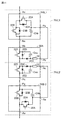
<サブモジュールの構成>
図2は、図1の各レグ回路を構成するサブモジュールの一例を示す回路図である。具体的には、図2(a)に示すサブモジュール7は、ハーフブリッジ構成と呼ばれる回路構成を有する。以下では、図2(a)の回路構成を有する「サブモジュール7」を「サブモジュール7HB」とも称する。<Sub-module configuration>
FIG. 2 is a circuit diagram showing an example of a sub-module constituting each leg circuit of FIG. Specifically, the sub-module 7 shown in FIG. 2A has a circuit configuration called a half bridge configuration. Hereinafter, the “sub-module 7” having the circuit configuration of FIG. 2A will also be referred to as “sub-module 7HB”.
サブモジュール7HBは、半導体回路35と、エネルギー蓄積要素であるキャパシタChbとを含む。半導体回路35は、直列接続された2つのスイッチング素子22A,22Bと、ダイオード23A,23Bとを含む。ダイオード23A,23Bは、スイッチング素子22A,22Bとそれぞれ逆並列(すなわち、並列かつ逆バイアス方向)に接続されるダイオードである。キャパシタChbは、半導体回路35と並列に接続され、直流電圧を保持する。
Sub-module 7HB includes a
スイッチング素子22Bの両端子を入出力端子26P,26Nとする。具体的には、スイッチング素子22A,22Bの接続ノードは高電位側の入出力端子26Pと接続される。スイッチング素子22BとキャパシタChbとの接続ノードは低電位側の入出力端子26Nと接続される。典型的には、入出力端子26Pは、正極側に隣接するサブモジュール7の入出力端子26Nと接続される。入出力端子26Nは、負極側に隣接するサブモジュール7の入出力端子26Pと接続される。
Both terminals of the
スイッチング素子22A、22Bのスイッチング動作により、サブモジュール7HBの入出力端子間にはキャパシタChbの両端電圧、および零電圧が出力される。例えば、スイッチング素子22Aがオン、かつスイッチング素子22Bがオフとなったときに、キャパシタChbの両端電圧が出力される。スイッチング素子22Aがオフ、かつスイッチング素子22Bがオンとなったときに、零電圧が出力される。
By the switching operation of the
図2(b)に示すサブモジュール7は、図2(a)に示す回路にさらに他の回路を追加した回路構成を有する。以下では、図2(b)に示す回路構成を有する「サブモジュール7」を「サブモジュール7SU」とも称する。
The
サブモジュール7SUは、半導体回路31と、キャパシタChbと、半導体回路32とを含む。半導体回路31、キャパシタChb、および半導体回路32は、互いに並列接続されている。半導体回路31は、図2(a)の半導体回路35と同一である。そのため、サブモジュール7SUは、概ねサブモジュール7HBに半導体回路32を追加した回路構成を有する。
Sub-module 7SU includes
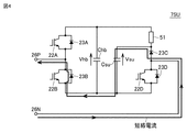
半導体回路32は、直列回路41と、キャパシタCsuと、抵抗素子51とを含む。直列回路41は、直列接続された、スイッチング素子22Dと、直流回路14の短絡事故時における短絡電流を流す半導体素子であるダイオード23Cとを含む。キャパシタCsuは、直列回路41に並列接続されたエネルギー蓄積要素である。抵抗素子51は、直列回路41とキャパシタCsuとを有する並列回路45に直列接続されている。また、ダイオード23Dは、スイッチング素子22Dと逆並列に接続されるダイオードである。詳細は後述するが、半導体回路32は、直流回路14での短絡事故発生時に流れる事故電流を抑制する機能を有する。
The
スイッチング素子22Aおよび22Bの接続ノードは高電位側の入出力端子26Pと接続され、スイッチング素子22Dとダイオード23Cとの接続ノードは低電位側の入出力端子26Nと接続される。
The connection node of the
正常な電力変換運転時は、スイッチング素子22Dは常時オンであり、スイッチング素子22A、22Bのスイッチング動作により、サブモジュール7SUの入出力端子間にはキャパシタChbの両端電圧、および零電圧が出力される。例えば、スイッチング素子22Aがオン、かつスイッチング素子22Bがオフとなったときに、キャパシタChbの両端電圧が出力される。スイッチング素子22Aがオフ、かつスイッチング素子22Bがオンとなったときに、零電圧が出力される。
During normal power conversion operation, the
図2(a)および図2(b)における各スイッチング素子22A,22B,22Dには、オン動作とオフ動作の両方を制御可能な自己消弧型のスイッチング素子が用いられる。スイッチング素子22A,22B,22Dは、例えば、IGBT(Insulated Gate Bipolar Transistor)またはGCT(Gate Commutated Turn-off)サイリスタ、MOSFET(Metal Oxide Semiconductor Field-Effect Transistor)などの自己消弧型の半導体スイッチング素子である。
For each of the
図2(a)および図2(b)において、キャパシタChb,Csuには、金属蒸着フィルムコンデンサなどのキャパシタが主に用いられる。以下の説明では、キャパシタChbの両端電圧は電圧Vhbとも称され、キャパシタCsuの両端電圧は電圧Vsuとも称される。 2A and 2B, capacitors such as metal vapor deposition film capacitors are mainly used as the capacitors Chb and Csu. In the following description, the voltage across the capacitor Chb is also referred to as the voltage Vhb, and the voltage across the capacitor Csu is also referred to as the voltage Vsu.
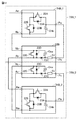
<直流回路の短絡事故時の電流経路>
実施の形態1では、複数のサブモジュール7のうちの規定数のサブモジュール7を、短絡事故電流を抑制する機能を有するサブモジュール7SUとして構成し、残りのサブモジュール7をサブモジュール7HBとして構成する。これにより、直流回路14の短絡事故時における短絡電流を抑制する。実施の形態1との比較のため、まず、複数のサブモジュール7のすべてがサブモジュール7HBで構成される比較例における短絡電流経路について説明する。<Current path in case of DC circuit short circuit accident>
In the first embodiment, a prescribed number of
図3は、比較例における短絡電流経路を示す図である。図3を参照して、直流回路14の内部を高電位側から低電位側に流れる短絡電流は、電力変換装置の内部を負極直流端子Nnから正極直流端子Npの方向に流れる。ここで、各レグ回路4u,4v,4wにおける上アーム5および下アーム6のうちどのアームを短絡電流が流れるかは、交流回路12と電力変換装置との間を流れる交流電流の位相によって異なる。図3の場合には、負極直流端子NnからV相の下アーム6を通って交流回路12に短絡電流が流れるとともに、交流回路12からU相の上アーム5を通って正極直流端子Npの方向に短絡電流が流れる。
FIG. 3 is a diagram showing a short-circuit current path in the comparative example. Referring to FIG. 3, a short-circuit current flowing from the high potential side to the low potential side inside
電力変換装置の制御装置は、各スイッチング素子に流れる電流を直接、あるいは間接的に検出する。典型的には、制御装置は、検出したアーム電流に基づいて、短絡が発生したと判定した場合、電力変換装置内の各スイッチング素子をオフにする。しかし、サブモジュール7HBのようなハーフブリッジ構成である場合、図2(a)に示すように、各スイッチング素子をオフにしても逆並列接続ダイオード(すなわち、ダイオード23B)が存在するため、入出力端子26Nから入出力端子26Pへの方向の短絡電流経路が維持され、過大な短絡電流が流れてしまう。
The control device of the power conversion device directly or indirectly detects the current flowing through each switching element. Typically, the control device turns off each switching element in the power conversion device when it is determined that a short circuit has occurred based on the detected arm current. However, in the case of a half-bridge configuration like the sub-module 7HB, as shown in FIG. 2A, even if each switching element is turned off, the anti-parallel connection diode (that is, the
次に、サブモジュール7SUを用いる構成について説明する。
図4は、実施の形態1に従うサブモジュール7SU内の短絡電流経路を示す図である。ここでは、キャパシタChbの電圧Vhbと、キャパシタCsuの電圧Vsuとはほぼ同一となっているものとする。Next, a configuration using the sub module 7SU will be described.
FIG. 4 is a diagram showing a short-circuit current path in submodule 7SU according to the first embodiment. Here, it is assumed that the voltage Vhb of the capacitor Chb and the voltage Vsu of the capacitor Csu are substantially the same.
図4を参照して、例えば、制御装置3は、検出されたアーム電流Iarmに基づいて、直流回路14に短絡事故が発生したと判定した場合、各スイッチング素子22A,22B,22Dをオフにする。これにより、図4に示すように、短絡電流は、入出力端子26N、ダイオード23C、キャパシタCsu、ダイオード23B、入出力端子26Pの経路で流れる。
With reference to FIG. 4, for example, when the
この場合、サブモジュール7SUの入出力端子26P,26N間の電圧が電圧Vsuよりも大きくなければ、ダイオード23B,23Cは導通しないため、短絡電流は流れない。すなわち、入出力端子26P,26N間の電圧が電圧Vsu以下であれば、短絡電流を抑制できる。入出力端子26P,26Nは直列に接続されているため、全体で考えると、交流回路12の電圧(例えば、交流系統電圧)の方が短絡電流経路上に存在するキャパシタCsuの電圧Vsuの総和以下であれば短絡電流を抑制できる。仮に、一時的に短絡電流が流れたとしてもキャパシタCsuを充電して電圧Vsuがさらに上昇するので短絡電流を減少させるように働き、最終的には抑制できる。
In this case, unless the voltage between the input/
なお、上記において、ダイオード23Cは、通常制御時(すなわち、入出力端子26P,26N間に零電圧または電圧Vhbを出力する場合)に抵抗素子51を介して電流が流れるのを防止するとともに、図4に示す短絡電流をキャパシタCsu側に流す機能を有している。そのため、ダイオード23Cの代わりに、それと同様の機能を有する他の半導体素子を用いてもよい。
In the above description, the
また、抵抗素子51は、キャパシタChbの正極性側と、短い時間領域においてキャパシタCsuの正極性側とが同電位にならないようにして、キャパシタChbとキャパシタCsuとを分離する役割を有している。そのため、抵抗素子51の代わりに、それと同様の役割を担う、抵抗成分を有する他の素子を用いてもよい。例えば、抵抗素子51は、リアクトルまたはダイオードと代替することができる。この場合、ダイオードのアノードはキャパシタChbの正極側に設けられ、ダイオードのカソードはダイオード23C側に設けられる。
Further, the
図5は、実施の形態1に従うレグ回路の構成を示す図である。図5を参照して、各レグ回路4の上アーム5に含まれる各サブモジュール7をサブモジュール7SUとして構成し、下アーム6に含まれる各サブモジュール7をサブモジュール7HBとして構成する。
FIG. 5 is a diagram showing a configuration of the leg circuit according to the first embodiment. Referring to FIG. 5, each sub-module 7 included in the
上述したように、交流回路12の最大電圧が電圧Vsuの総和以下であれば入出力端子26Nから入出力端子26Pの方向に流れる短絡電流を抑制できる。なお、入出力端子26Pから入出力端子26Nの方向に短絡電流を流そうとする交流電圧は、電圧Vhbによりブロックされる。ここで、レグ回路4に含まれるすべてのサブモジュール7の台数をN台とすると、交流回路12の電圧の最大値は、概ねN/2台分のサブモジュール7の電圧Vhbの総和に対応する。ここで、電圧Vhbと電圧Vsuとは同一である。したがって、電圧Vsuを出力するサブモジュール7SUをN/2台以上用意すれば、交流回路12の電圧が電圧Vsuの総和以下となるため、短絡電流を抑制することができる。
As described above, if the maximum voltage of the
典型的には、上アーム5内のサブモジュール数と下アーム5内のサブモジュール数とは同数である。そのため、例えば、図5に示すように上アーム5内のすべてのサブモジュール7をサブモジュール7SUとすることで短絡電流を抑制できる。
Typically, the number of sub-modules in the
より具体的には、短絡電流を抑制するためには、交流回路12の電圧の最大値をキャパシタCsuの電圧Vsuで除算した数(すなわち、「交流回路の電圧の最大値」÷「電圧Vsu」で求められるサブモジュール数)よりも多くのサブモジュール7SUを短絡電流経路内に有していればよい。以下、この除算した数を「算出数K」とも称する。レグ回路4は、算出数Kのサブモジュール7SUを有していればよく、上アーム5および下アーム6に含まれるサブモジュール7SUの数の比率は任意である。
More specifically, in order to suppress the short-circuit current, the maximum value of the voltage of the
実施の形態1では、直流回路14の短絡事故の保護に必要な台数のサブモジュール7SUを使用し、これ以外はハーフブリッジ構成のサブモジュール7HBを使用する構成とすることで、直流回路14の短絡によって生じる過電流を抑制できる。また、サブモジュール7SUでは、電力変換用のキャパシタChbと、短絡電流の抑制用のキャパシタCsuとを独自に有している。そのため、電力変換に適したキャパシタChbと、短絡電流の抑制に適したキャパシタCsuとを個別に設計することができ、設計自由度が向上する。したがって、直流回路14の短絡電流をより容易に抑制できる。
In the first embodiment, the short circuit of the
また、実施の形態1では、算出数Kを求めることによって、サブモジュール7SUの台数を必要最小限に抑えることができるため、構成の簡素化を図ることもできる。また、より小容量(例えば、キャパシタChbよりも小容量)のキャパシタCsuを用いれば、電圧Vsuを大きくすることができる。そのため、この場合、直流回路14の短絡事故の保護に必要なサブモジュール7SUの台数を減らすことができる。ただし、短絡電流の抑制という観点では、例えば、レグ回路4内のすべてのサブモジュール7を、サブモジュール7SUで構成してもよい。
In addition, in the first embodiment, by obtaining the calculated number K, the number of sub-modules 7SU can be suppressed to the necessary minimum, so that the configuration can be simplified. Further, the voltage Vsu can be increased by using the capacitor Csu having a smaller capacity (for example, a capacity smaller than the capacitor Chb). Therefore, in this case, the number of sub-modules 7SU required to protect the
<処理手順>
図6は、実施の形態1に従う制御装置3の処理手順を示すフローチャートである。典型的には、以下の各ステップは、制御装置3の演算部によって実行される。<Processing procedure>
FIG. 6 is a flowchart showing a processing procedure of
制御装置3は、電力変換器2の初期充電(すなわち、各キャパシタChb,Csuの初期充電)が完了すると、運転開始指令を出力して通常制御を行なう(ステップS10)。具体的には、制御装置3は、各レグ回路4に含まれる各サブモジュール7の出力電圧を制御する。この場合、サブモジュール7SUにおいては、スイッチング素子22Dを常時オンとし、スイッチング素子22A,22Bをオンオフすることで出力電圧が制御される。
When the initial charging of power converter 2 (that is, the initial charging of capacitors Chb and Csu) is completed,
次に、制御装置3は、サブモジュール7に流れる電流に基づいて、直流回路14の短絡事故が発生したか否かを判定する(ステップS12)。例えば、制御装置3は、アーム電流検出器9A,9Bにより検出された各アーム電流Ipu,Ipv,Ipw,Inu,Inv,Inwの絶対値の少なくとも1つが閾値を超えている場合、あるいは、アーム電流の各相合計値が閾値を超えている場合に、直流回路14の短絡事故が発生したと判定する。なお、サブモジュール7に流れる電流を検出するために、直流回路14の正極端子側に電流検出器を設ける場合には、制御装置3は、当該電流検出器により検出された直流電流を用いて短絡事故の発生の有無を判定してもよい。例えば、制御装置3は、検出された直流電流が閾値を超えた場合に、短絡事故が発生したと判定する。
Next, the
短絡事故が発生していない場合(ステップS12においてNO)、制御装置3はステップS10の処理を実行する。短絡事故が発生した場合(ステップS12においてYES)、制御装置3は、電力変換器2の各レグ回路4に含まれるすべてのサブモジュール7のスイッチング素子(例えば、スイッチング素子22A,22B,22D)をオフにする(ステップS14)。この場合、上述したように、各レグ回路4は、算出数K以上のサブモジュール7SUを有しているため、直流回路14の短絡電流が抑制される。
When no short circuit accident has occurred (NO in step S12),
<利点>
実施の形態1によると、電力変換用のキャパシタと、短絡電流の抑制用のキャパシタとを独自に有している。したがって、電力変換に適したキャパシタと、短絡電流の抑制に適したキャパシタとを個別に設計できるため、直流回路の短絡事故によって生じる事故電流を容易に抑制できる。結果として、サブモジュール内の素子の破損を防ぐことができる。<Advantages>
According to the first embodiment, the power conversion capacitor and the short-circuit current suppressing capacitor are independently provided. Therefore, the capacitor suitable for power conversion and the capacitor suitable for suppressing the short-circuit current can be individually designed, so that the accident current caused by the short-circuit accident of the DC circuit can be easily suppressed. As a result, damage to the elements in the submodule can be prevented.
実施の形態2.
実施の形態1では、各サブモジュール7に流れる短絡電流を抑制することにより、サブモジュール内の素子の破損を防ぐ構成について説明した。実施の形態2では、サブモジュール7SUを用いて、バイパス回路に短絡電流を転流する構成について説明する。
In the first embodiment, the configuration in which the element in the submodule is prevented from being damaged by suppressing the short-circuit current flowing in each
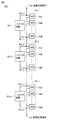
図7は、実施の形態2に従うレグ回路4の構成を示す図である。図7を参照して、各レグ回路4において、上アーム5に含まれる複数のサブモジュール7のうちの1つはサブモジュール7SUで構成されており、それ以外のサブモジュール7はサブモジュール7HBで構成されている。上アーム5は、バイパス回路80と電気的に並列に(すなわち、上アーム5の外部接続ノード40pと40nとの間に)接続されている。下アーム6においても、複数のサブモジュール7のうちの1つはサブモジュール7SUで構成されており、それ以外のサブモジュール7はサブモジュール7HBで構成されている。下アーム6は、バイパス回路80と電気的に並列に接続されている。
FIG. 7 is a diagram showing a configuration of the leg circuit 4 according to the second embodiment. Referring to FIG. 7, in each leg circuit 4, one of the plurality of
各バイパス回路80は、直流回路14の短絡事故時に、各アームを流れる短絡電流を転流するために設けられている。短絡電流は、各アームの低電位側端子から高電位側端子の方向(すなわち、各アームの低電位側の外部接続ノード40nから高電位側の外部接続ノード40pの方向)に流れるため、バイパス回路80はこの方向に直流電流を流すように構成される。
Each
直流回路14の正常時には、高電位側端子が低電位側端子よりも高電位となるように(すなわち、各アームの外部接続ノード40pが高電位側となり、外部接続ノード40nが低電位側となるように)直流電圧がかかる。したがって、各バイパス回路80は、高電位側端子から低電位側端子の方向の電流を阻止するように構成される。これによって、直流回路14の正常時の各アームの動作が妨げられないようにする。典型的には、バイパス回路80は、負極直流端子Nnから正極直流端子Npの方向が順方向となるように配置された少なくとも1つのダイオードを含む。
When the
実施の形態1で説明したように、直流回路14の短絡事故時には、各サブモジュール7のスイッチング素子22A,22B,22Dはオフにされる。また、サブモジュール7SUは、短絡電流を抑制する電圧を発生させるキャパシタCsuを有している。そのため、各アームに含まれる複数のサブモジュール7のうちの少なくとも1つをサブモジュール7SUで構成することにより、直流回路14の短絡事故時において当該アームの両端(すなわち、外部接続ノード40pと40nとの間)には短絡電流を抑制する電圧が発生する。したがって、図7に示すように短絡電流はアーム内のサブモジュール7を流れることなく、バイパス回路80側に転流される。したがって、各アームに短絡電流が流れることはない。この結果、各サブモジュール7を構成する素子が保護される。
As described in the first embodiment, the
図8は、実施の形態2に従うバイパス回路の構成例を示す回路図である。図8(a)を参照して、バイパス回路80は、互いに直列接続された複数のダイオード82を含む。各ダイオード82のカソードは高電位側に設けられ、各ダイオード82のアノードは低電位側に設けられる。すなわち、低電位側の外部接続ノード40nから高電位側の外部接続ノード40pの方向(すなわち、負極直流端子Nnから正極直流端子Npの方向)が、各ダイオード82の順方向となる。
FIG. 8 is a circuit diagram showing a configuration example of the bypass circuit according to the second embodiment. Referring to FIG. 8A,
直流回路14の短絡事故時には、低電位側の外部接続ノード40nから高電位側の外部接続ノード40pの方向に短絡電流が流れるので、短絡電流を各バイパス回路80の複数のダイオード82を介して流すことができる。これによって、各サブモジュール7を保護する。一方、直流回路14の正常時において、外部接続ノード40pが高電位側となり外部接続ノード40nが低電位側となるように直流電圧が印加される場合には、各ダイオード82に対して逆方向となるのでバイパス回路80に電流が流れることはない。
In the event of a short circuit in the
バイパス回路80を構成する各ダイオード82に特性のばらつきがある場合には、ダイオード82ごとの電圧の分担に違いが生じるために、他よりも大きな電圧がかかっているダイオード82が過電圧により破損する場合がある。この問題を回避するために、各ダイオード82としてアバランシェダイオードを用いるのが望ましい。アバランシェダイオードは、規定レベル以上の電圧がアノード−カソード間に印加されると破損する前に漏れ電流が増加する。これによって、自己の電圧上昇を抑え、他のダイオード82に電圧を分担させることができる。
When the
図8(b)には、図8(a)の変形例が示されている。図8(b)のバイパス回路80は、複数のダイオード82とそれぞれ並列に接続された抵抗素子83を含む点で、図8(a)のバイパス回路80と異なる。各抵抗素子83の抵抗値は互いにほぼ等しい値に設定される。さらに、抵抗素子83の抵抗値は、電力系統の正常時に高電位側の外部接続ノード40pから低電位側の外部接続ノード40nの方向に各抵抗素子83を介して電流がほとんど流れないように、比較的高い値に設定される。各抵抗素子83の抵抗値をほぼ等しい値にすることによって、ダイオード82ごとに分担される電圧をほぼ等しくすることができ、これによって、ダイオード82の破損を防止することができる。
FIG. 8(b) shows a modification of FIG. 8(a). The
上記の図7の例では、各アームに1つのバイパス回路80を並列接続する構成について説明したが、当該構成に限られない。各アーム内の一定数のサブモジュール7(以下、「サブモジュール群」とも称する。)に対して、バイパス回路80を並列接続する構成であってもよい。
In the example of FIG. 7 described above, the configuration in which one
図9は、実施の形態2の変形例に従うバイパス回路の構成例を示す図である。図9では、上アーム5および下アーム6にそれぞれ接続されるリアクトル8A,8Bは図示していない。上アーム5の場合、高電位側端子15pは図1の正極直流端子Npに対応し、低電位側端子15nは交流端子NuまたはNvまたはNwに対応する。下アーム6の場合、高電位側端子15pは図1の交流端子NuまたはNvまたはNwに対応し、低電位側端子15nは負極直流端子Nnに対応する。
FIG. 9 is a diagram showing a configuration example of a bypass circuit according to the modification of the second embodiment. In FIG. 9, the
図9を参照して、各アームは、高電位側のサブモジュール群20_1から低電位側のサブモジュール群20_mまでのカスケード接続されたm個(mは1以上の整数)のサブモジュール群20_1〜20_mを含む。サブモジュール群20_1〜20_mについて、総称する場合、サブモジュール群20と記載する。各アームを構成するサブモジュール群20が1個の場合の例が、図7の例に対応する。 Referring to FIG. 9, each arm includes m (m is an integer of 1 or more) sub-module groups 20_1 to cascade-connected from the high-potential side sub-module group 20_1 to the low-potential side sub-module group 20_m. Including 20_m. The sub-module groups 20_1 to 20_m are collectively referred to as the sub-module group 20. An example in which there is one sub-module group 20 forming each arm corresponds to the example in FIG. 7.
第i番目のサブモジュール群20_i(iは、1≦i≦mを満たす任意の整数)は、他のサブモジュール群20と接続するための高電位側の外部接続ノード40p_iおよび低電位側の外部接続ノード40n_iと、外部接続ノード40p_iと40n_iとの間にカスケード接続された複数個のサブモジュール7(7SU,7HB)とを含む。外部接続ノード40p_i,40n_iについて総称する場合、それぞれ外部接続ノード40p,40nと記載する。
The i-th sub-module group 20_i (i is an arbitrary integer satisfying 1≦i≦m) is a high-potential-side external connection node 40p_i and a low-potential-side external connection node for connecting to another sub-module group 20. It includes a connection node 40n_i and a plurality of sub-modules 7 (7SU, 7HB) cascade-connected between the external connection nodes 40p_i and 40n_i. The external connection nodes 40p_i and 40n_i are collectively referred to as
各サブモジュール群20は、サブモジュール7として、1以上のサブモジュール7SUと、1以上のサブモジュール7HBとを含む。図9では、1個のサブモジュール7SUおよび複数のサブモジュール7HBによって各サブモジュール群20が構成される例が示されている。各サブモジュール群20に含まれるサブモジュール7の数は、サブモジュール群20ごとに異なっていてもよい。各サブモジュール群20に含まれるサブモジュール7SUとサブモジュール7HBとの配列順は、サブモジュール群20ごとに異なっていてもよい。
Each submodule group 20 includes, as the
各アームは、さらに、m個のサブモジュール群20_1〜20_mにそれぞれ対応するm個のバイパス回路80_1〜80_mを含む(総称する場合、バイパス回路80と記載する)。m個のバイパス回路80_は、高電位側のバイパス回路80_1から低電位側のバイパス回路80_mまでによって構成される。各バイパス回路80は対応するサブモジュール群20と電気的に並列に(すなわち、対応するサブモジュール群20の外部接続ノード40pと40nとの間に)接続されている。
Each arm further includes m bypass circuits 80_1 to 80_m corresponding to the m sub-module groups 20_1 to 20_m (collectively referred to as bypass circuit 80). The m bypass circuits 80_ are composed of the bypass circuits 80_1 on the high potential side to the bypass circuits 80_m on the low potential side. Each
直流回路14の短絡事故時には、各サブモジュール7のスイッチング素子22A,22B,22Dはオフにされる。また、図9のサブモジュール群20には、少なくとも1つのサブモジュール7SUが含まれる。そのため、直流回路14の短絡事故時における短絡電流は、サブモジュール群20に流れることなく、バイパス回路80側に転流される。この結果、各サブモジュール7を構成する素子が保護される。
In the event of a short circuit in the
<利点>
実施の形態2によると、直流回路の短絡事故によって生じる事故電流をバイパス回路に転流することができる。結果として、サブモジュール内の半導体素子の破損を防ぐことができる。また、実施の形態1の構成例よりも、サブモジュール7SUの個数を全体として削減することができる。<Advantages>
According to the second embodiment, the fault current generated by the short circuit fault of the DC circuit can be commutated to the bypass circuit. As a result, it is possible to prevent the semiconductor element in the submodule from being damaged. Further, the number of submodules 7SU can be reduced as a whole as compared with the configuration example of the first embodiment.
その他の実施の形態.
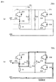
(1)上述した実施の形態において、サブモジュール7HBと半導体回路32とを組み合わせることで、サブモジュール7SUに相当する回路を設けてもよい。Other embodiments.
(1) In the embodiment described above, a circuit corresponding to the submodule 7SU may be provided by combining the submodule 7HB and the
図10は、その他の実施の形態に従うサブモジュール7の回路構成例(その1)を示す図である。図10を参照して、サブモジュール7HBに半導体回路32が接続されている。具体的には、サブモジュール7HBの正極端子Paと、半導体回路32の正極端子Pbとが接続され、サブモジュール7HBの負極端子Naと、半導体回路32の負極端子Nbとが接続される。サブモジュール7HBの端子Aaが図2のサブモジュール7SUの高電位側の入出力端子26Pに対応し、半導体回路32の端子Abが図2のサブモジュール7SUの低電位側の入出力端子26Nに対応する。このように、サブモジュール7HBと半導体回路32とを組み合わせることによりサブモジュール7SUを構成できる。この場合、既存のサブモジュール7HBに半導体回路32を追加接続するだけでサブモジュール7SUを構成することができる。
FIG. 10 is a diagram showing a circuit configuration example (No. 1) of the
図11は、その他の実施の形態に従うサブモジュール7の回路構成例(その2)を示す図である。図11を参照して、ハーフブリッジ構成の2つのサブモジュール7HB_1および7HB_2と、1つの半導体モジュール32Aとが接続されている。半導体モジュール32Aは、2つの半導体回路32を組み合わせた構成を有している。
FIG. 11 is a diagram showing a circuit configuration example (No. 2) of the
具体的には、サブモジュール7HB_1の正極端子Paと、半導体モジュール32Aの正極端子Pbとが接続され、サブモジュール7HB_1の負極端子Naと、半導体モジュール32Aの負極端子Nbとが接続される。サブモジュール7HB_2の正極端子Paと、半導体モジュール32Aの正極端子Pcとが接続され、サブモジュール7HB_2の負極端子Naと、半導体モジュール32Aの負極端子Ncとが接続される。
Specifically, the positive terminal Pa of the sub-module 7HB_1 is connected to the positive terminal Pb of the
図11の構成例では、サブモジュール7HB_1と、半導体モジュール32Aのうちの上側の半導体回路32とで構成される回路が、サブモジュール7SUの回路に対応する(図中のサブモジュール7SU_1に対応)。また、サブモジュール7HB_2と、半導体モジュール32Aのうちの下側の半導体回路32とで構成される回路が、サブモジュール7SUの回路に対応する(図中のサブモジュール7SU_2に対応)。サブモジュール7HB_1の端子Aaが高電位側の入出力端子に対応し、サブモジュール7HB_2の端子Aaが低電位側の入出力端子に対応する。
In the configuration example of FIG. 11, the circuit configured by the sub-module 7HB_1 and the
キャパシタCsuとして小容量のコンデンサを選択することにより、半導体回路32の体積を小さくできる。この場合、図11の構成例のように、半導体回路32がサブモジュール7HBに比べて体積を小さくできるという利点を利用し、2つの半導体回路32を1つのモジュール(すなわち、半導体モジュール32A)に収納できる。
The volume of the
図12は、その他の実施の形態に従うサブモジュール7の回路構成例(その3)を示す図である。図12の構成例は、図11の構成例と基本的には同様であり、上側のサブモジュール7HB_1の回路構成と、下側のサブモジュール7HB_2の回路構成を同一にしたものである。ハーフブリッジ構成の2つのサブモジュール7HB_1および7HB_2と、1つの半導体モジュール32Bとが接続されている。半導体モジュール32Bは、2つの半導体回路32を組み合わせた構成を有している。
FIG. 12 is a diagram showing a circuit configuration example (No. 3) of the
図12の構成例では、サブモジュール7HB_1と、半導体モジュール32Bのうちの上側の半導体回路32とで構成される回路が、サブモジュール7SUの回路に対応(図中のサブモジュール7SU_1に対応)する。また、サブモジュール7HB_2と、半導体モジュール32Bのうちの下側の半導体回路32とで構成される回路が、サブモジュール7SUの回路に対応(図中のサブモジュール7SU_2に対応)する。サブモジュール7HB_1の端子Aaが高電位側の入出力端子に対応し、半導体モジュール32Bの端子Acが低電位側の入出力端子に対応する。
In the configuration example of FIG. 12, the circuit configured by the sub-module 7HB_1 and the
(2)上述した実施の形態において、短絡電流の抑制用のサブモジュール7は、図2(b)のような回路構成である場合について説明したが、当該回路構成に限られず、例えば、図13に示すような回路構成であってもよい。 (2) In the above-described embodiment, the case where the short-circuit current suppressing sub-module 7 has a circuit configuration as shown in FIG. 2B has been described, but the present invention is not limited to this circuit configuration, and for example, FIG. The circuit configuration as shown in FIG.
図13は、短絡事故電流を抑制する機能を有するサブモジュールの回路構成の他の例を示す図である。ここでは、図13に示す回路構成を有する「サブモジュール7」を「サブモジュール7SUx」とも称する。 FIG. 13 is a diagram showing another example of the circuit configuration of the sub-module having the function of suppressing the short-circuit fault current. Here, the "sub-module 7" having the circuit configuration shown in FIG. 13 is also referred to as "sub-module 7SUx".
図13(a)を参照して、サブモジュール7SUxは、図2(b)に示すサブモジュール7SUと同様に、直流回路14の短絡事故時における短絡電流を抑制する機能を有する。具体的には、サブモジュール7SUxは、半導体回路31xと、キャパシタChbと、半導体回路32xとを含む。半導体回路31x、キャパシタChb、および半導体回路32xは、互いに並列接続されている。
With reference to FIG. 13A, the submodule 7SUx has a function of suppressing a short-circuit current at the time of a short circuit accident of the
半導体回路31xは、直列接続された2つのスイッチング素子22A,22Bと、ダイオード23A,23Bとを含む。ダイオード23A,23Bは、スイッチング素子22A,22Bとそれぞれ逆並列に接続される。
The
半導体回路32xは、直列回路41xと、キャパシタCsuと、抵抗素子51とを含む。直列回路41xは、直列接続された、スイッチング素子22Dと、短絡電流を流す半導体素子であるダイオード23Cとを含む。キャパシタCsuは、直列回路41xに並列接続されたエネルギー蓄積要素である。抵抗素子51は、直列回路41xとキャパシタCsuとを有する並列回路45xに直列接続されている。また、ダイオード23Dは、スイッチング素子22Dと逆並列に接続されるダイオードである。半導体回路32xは、図2(b)の半導体回路32と同様に、直流回路14での短絡事故発生時に流れる事故電流を抑制する機能を有する。
The
スイッチング素子22Aおよび22Bの接続ノードは低電位側の入出力端子26Nと接続され、スイッチング素子22Dとダイオード23Cとの接続ノードは高電位側の入出力端子26Pと接続される。正常な電力変換運転時は、スイッチング素子22Dは常時オンである。この場合、スイッチング素子22Aがオンかつスイッチング素子22BがオフとなったときにキャパシタChbの両端電圧が出力され、スイッチング素子22Aがオフかつスイッチング素子22Bがオンとなったときに零電圧が出力される。
The connection node of the
図13(b)は、サブモジュール7SUx内の短絡電流経路を示している。ここでは、キャパシタChbの電圧Vhbと、キャパシタCsuの電圧Vsuとはほぼ同一となっているものとする。例えば、制御装置3は、検出されたアーム電流Iarmに基づいて、直流回路14に短絡事故が発生したと判定した場合、各スイッチング素子22A,22B,22Dをオフにする。これにより、図13(b)に示すように、短絡電流は、入出力端子26N、ダイオード23B、キャパシタCsu、ダイオード23C、入出力端子26Pの経路で流れる。
FIG. 13B shows a short circuit current path in the sub module 7SUx. Here, it is assumed that the voltage Vhb of the capacitor Chb and the voltage Vsu of the capacitor Csu are substantially the same. For example, when the
サブモジュール7SUxの短絡電流抑制機能は、サブモジュール7SUのそれと同様である。具体的には、入出力端子26P,26N間の電圧が電圧Vsu以下であれば、短絡電流を抑制できる。入出力端子26P,26Nは直列に接続されているため、全体で考えると、交流回路12の電圧(例えば、交流系統電圧)の方が短絡電流経路上に存在するキャパシタCsuの電圧Vsuの総和以下であれば短絡電流を抑制できる。
The short-circuit current suppressing function of the sub-module 7SUx is similar to that of the sub-module 7SU. Specifically, if the voltage between the input/
(3)上述の実施の形態として例示した構成は、本発明の構成の一例であり、別の公知の技術と組み合わせることも可能であるし、本発明の要旨を逸脱しない範囲で、一部を省略する等、変更して構成することも可能である。また、上述した実施の形態において、他の実施の形態で説明した処理および構成を適宜採用して実施する場合であってもよい。 (3) The configuration illustrated as the above-described embodiment is an example of the configuration of the present invention, and can be combined with another known technique, and a part thereof is not deviated from the scope not departing from the gist of the present invention. It is also possible to change the configuration such as omitting it. Further, in the above-described embodiment, the processes and configurations described in the other embodiments may be appropriately adopted and implemented.
今回開示された実施の形態はすべての点で例示であって制限的なものではないと考えられるべきである。本発明の範囲は、上記した説明ではなく、請求の範囲によって示され、請求の範囲と均等の意味および範囲内でのすべての変更が含まれることが意図される。 The embodiments disclosed this time are to be considered as illustrative in all points and not restrictive. The scope of the present invention is shown not by the above description but by the claims, and is intended to include meanings equivalent to the claims and all modifications within the scope.
1 電力変換装置、2 電力変換器、3 制御装置、4u,4v,4w レグ回路、5 上アーム、6 下アーム、7,7HB,7SU,7SUx サブモジュール、8A,8B リアクトル、9A,9B アーム電流検出器、10 交流電圧検出器、11A,11B 直流電圧検出器、12 交流回路、13 変圧器、14 直流回路、15n 低電位側端子、15p 高電位側端子、16 交流電流検出器、20 サブモジュール群、22A,22B,22D スイッチング素子、23A,23B,23C,23D,82 ダイオード、26N,26P 入出力端子、31,31x,32,32x,35 半導体回路、32A,32B 半導体モジュール、40n,40p 外部接続ノード、41,41x 直列回路、45,45x 並列回路、51,83 抵抗素子、80 バイパス回路、Nn 負極直流端子、Np 正極直流端子、Nu,Nv,Nw 交流端子。 1 power converter, 2 power converter, 3 controller, 4u, 4v, 4w leg circuit, 5 upper arm, 6 lower arm, 7,7HB, 7SU, 7SUx submodule, 8A, 8B reactor, 9A, 9B arm current Detector, 10 AC voltage detector, 11A, 11B DC voltage detector, 12 AC circuit, 13 transformer, 14 DC circuit, 15n low potential side terminal, 15p high potential side terminal, 16 AC current detector, 20 sub-module Group, 22A, 22B, 22D switching element, 23A, 23B, 23C, 23D, 82 diode, 26N, 26P input/output terminal, 31, 31x, 32, 32x, 35 semiconductor circuit, 32A, 32B semiconductor module, 40n, 40p external Connection node, 41, 41x series circuit, 45, 45x parallel circuit, 51, 83 resistance element, 80 bypass circuit, Nn negative DC terminal, Np positive DC terminal, Nu, Nv, Nw AC terminal.
Claims (8)
直列接続された複数のサブモジュールを含むレグ回路を備え、
前記複数のサブモジュールのうちの少なくとも1つは第1サブモジュールであり、
前記第1サブモジュールは、第1エネルギー蓄積要素と、直列接続された2つのスイッチング素子を有する第1半導体回路と、第2半導体回路とを含み、
前記第1エネルギー蓄積要素、前記第1半導体回路、および前記第2半導体回路は、互いに並列接続されており、
前記第2半導体回路は、
直列接続されたスイッチング素子と半導体素子とを含む直列回路と、
前記直列回路に並列接続された第2エネルギー蓄積要素と、
前記直列回路および前記第2エネルギー蓄積要素を含む並列回路に直列接続された抵抗成分を有する素子とを含む、電力変換装置。A power conversion device for converting power between a DC circuit and an AC circuit,
A leg circuit including a plurality of sub-modules connected in series,
At least one of the plurality of sub-modules is a first sub-module,
The first sub-module includes a first energy storage element, a first semiconductor circuit having two switching elements connected in series, and a second semiconductor circuit,
The first energy storage element, the first semiconductor circuit, and the second semiconductor circuit are connected in parallel to each other,
The second semiconductor circuit is
A series circuit including a switching element and a semiconductor element connected in series,
A second energy storage element connected in parallel with the series circuit;
A power conversion device, comprising: an element having a resistance component connected in series to a parallel circuit including the series circuit and the second energy storage element.
前記第1アームおよび前記第2アームの各々は、1以上のサブモジュール群を含み、
前記1以上のサブモジュール群の各々は、バイパス回路と並列接続されており、
前記1以上のサブモジュール群の各々は、1以上の前記第1サブモジュールと、1以上の第2サブモジュールとを含み、
前記第2サブモジュールは、エネルギー蓄積要素と、2つの半導体スイッチング素子を直列接続した半導体回路とが並列接続されたハーフブリッジ構成を有する、請求項1〜請求項4のいずれか1項に記載の電力変換装置。The leg circuit is connected to the AC connection part and the DC circuit, and a first arm provided between an AC connection part connected to the AC circuit and a positive electrode DC terminal connected to the DC circuit. A second arm provided between the negative electrode and the DC terminal,
Each of the first arm and the second arm includes one or more sub-module groups,
Each of the one or more sub-module groups is connected in parallel with a bypass circuit,
Each of the one or more sub-module groups includes one or more first sub-modules and one or more second sub-modules,
The said 2nd submodule has the half bridge structure in which the energy storage element and the semiconductor circuit which connected two semiconductor switching elements in series were connected in parallel, The any one of Claims 1-4 characterized by the above-mentioned. Power converter.
前記複数のサブモジュールの各々を制御する制御装置とをさらに備え、
前記制御装置は、
前記電流検出器により検出された電流に基づいて、前記直流回路の短絡事故が発生したか否かを判定し、
前記直流回路の短絡事故が発生した場合に、前記レグ回路の前記複数のサブモジュールに含まれるすべてのスイッチング素子をオフにする、請求項1〜請求項7のいずれか1項に記載の電力変換装置。A current detector for detecting a current flowing through the sub-module,
Further comprising a control device for controlling each of the plurality of sub-modules,
The control device is
Based on the current detected by the current detector, to determine whether a short circuit accident of the DC circuit has occurred,
The power conversion according to any one of claims 1 to 7, wherein all the switching elements included in the plurality of sub-modules of the leg circuit are turned off when a short circuit accident of the DC circuit occurs. apparatus.
Applications Claiming Priority (1)
| Application Number | Priority Date | Filing Date | Title |
|---|---|---|---|
| PCT/JP2019/047263 WO2021111526A1 (en) | 2019-12-03 | 2019-12-03 | Power conversion device |
Publications (2)
| Publication Number | Publication Date |
|---|---|
| JP6719692B1 true JP6719692B1 (en) | 2020-07-08 |
| JPWO2021111526A1 JPWO2021111526A1 (en) | 2021-12-02 |
Family
ID=71402374
Family Applications (1)
| Application Number | Title | Priority Date | Filing Date |
|---|---|---|---|
| JP2020512896A Active JP6719692B1 (en) | 2019-12-03 | 2019-12-03 | Power converter |
Country Status (4)
| Country | Link |
|---|---|
| US (1) | US20220385209A1 (en) |
| EP (1) | EP4071996A4 (en) |
| JP (1) | JP6719692B1 (en) |
| WO (1) | WO2021111526A1 (en) |
Citations (5)
| Publication number | Priority date | Publication date | Assignee | Title |
|---|---|---|---|---|
| JP2013121223A (en) * | 2011-12-07 | 2013-06-17 | Hitachi Ltd | Power converter |
| WO2017168519A1 (en) * | 2016-03-28 | 2017-10-05 | 三菱電機株式会社 | Power conversion device |
| JP6345379B1 (en) * | 2017-08-09 | 2018-06-20 | 三菱電機株式会社 | Power converter |
| JP2019022313A (en) * | 2017-07-14 | 2019-02-07 | 株式会社東芝 | Power conversion device |
| WO2019064705A1 (en) * | 2017-09-26 | 2019-04-04 | 三菱電機株式会社 | Power conversion device |
Family Cites Families (14)
| Publication number | Priority date | Publication date | Assignee | Title |
|---|---|---|---|---|
| DE102009057288B4 (en) * | 2009-12-01 | 2018-02-15 | Siemens Aktiengesellschaft | Inverters for high voltages |
| BR112012023451A2 (en) * | 2010-03-18 | 2016-05-24 | Abb Research Ltd | converter cell for cascade converters and a control system and method for operating a converter cell |
| EP2747267B1 (en) * | 2012-12-18 | 2020-02-05 | General Electric Technology GmbH | Electrical apparatus including chain-link converter and protection circuit |
| EP2946464B1 (en) | 2013-01-21 | 2019-12-18 | ABB Schweiz AG | A multilevel converter with hybrid full-bridge cells |
| US20160036314A1 (en) * | 2013-03-18 | 2016-02-04 | Mitsubishi Electric Corporation | Power conversion apparatus |
| DE102013219466A1 (en) * | 2013-09-26 | 2015-03-26 | Siemens Aktiengesellschaft | Multilevelumrichter |
| CN105099242B (en) * | 2014-05-09 | 2018-09-11 | 南京南瑞继保电气有限公司 | Voltage-source type multilevel converter, DC transmission system, fault handling method and device |
| US9871437B2 (en) * | 2014-07-10 | 2018-01-16 | University-Industry Foundation(UIF) | Fault current reduction structure of multi-level converter and apparatus using the fault current reduction structure |
| DE102015105889A1 (en) * | 2015-04-17 | 2016-10-20 | Ge Energy Power Conversion Technology Limited | Switching module and converter with at least one switching module |
| US10326355B2 (en) * | 2015-07-14 | 2019-06-18 | Mitsubishi Electric Corporation | Power conversion device |
| EP3255773B1 (en) * | 2016-06-09 | 2021-01-13 | GE Energy Power Conversion Technology Ltd. | Low loss double submodule for a modular multi-level converter and modular multi-level converter having same |
| WO2018154783A1 (en) * | 2017-02-27 | 2018-08-30 | 三菱電機株式会社 | Electric power conversion apparatus and dc power transmission system |
| JP6440923B1 (en) * | 2017-09-26 | 2018-12-19 | 三菱電機株式会社 | Power converter |
| EP3780366A1 (en) * | 2019-08-13 | 2021-02-17 | Vestas Wind Systems A/S | Dc chopper for mmc cell with integrated chopper resistor |
-
2019
- 2019-12-03 WO PCT/JP2019/047263 patent/WO2021111526A1/en unknown
- 2019-12-03 EP EP19955250.6A patent/EP4071996A4/en active Pending
- 2019-12-03 US US17/772,686 patent/US20220385209A1/en active Pending
- 2019-12-03 JP JP2020512896A patent/JP6719692B1/en active Active
Patent Citations (5)
| Publication number | Priority date | Publication date | Assignee | Title |
|---|---|---|---|---|
| JP2013121223A (en) * | 2011-12-07 | 2013-06-17 | Hitachi Ltd | Power converter |
| WO2017168519A1 (en) * | 2016-03-28 | 2017-10-05 | 三菱電機株式会社 | Power conversion device |
| JP2019022313A (en) * | 2017-07-14 | 2019-02-07 | 株式会社東芝 | Power conversion device |
| JP6345379B1 (en) * | 2017-08-09 | 2018-06-20 | 三菱電機株式会社 | Power converter |
| WO2019064705A1 (en) * | 2017-09-26 | 2019-04-04 | 三菱電機株式会社 | Power conversion device |
Also Published As
| Publication number | Publication date |
|---|---|
| WO2021111526A1 (en) | 2021-06-10 |
| EP4071996A4 (en) | 2022-11-23 |
| JPWO2021111526A1 (en) | 2021-12-02 |
| US20220385209A1 (en) | 2022-12-01 |
| EP4071996A1 (en) | 2022-10-12 |
Similar Documents
| Publication | Publication Date | Title |
|---|---|---|
| EP2786479B1 (en) | Power converter | |
| US11159092B2 (en) | Power conversion device | |
| JP6180693B1 (en) | Power converter | |
| US10637371B2 (en) | Interface arrangement between an alternating current power system and a direct current power system with control of converter valve for fault protection | |
| JP6545425B1 (en) | Power converter | |
| RU2652690C2 (en) | Modular multi-point valve inverter for high voltages | |
| JPWO2019003290A1 (en) | Power converter | |
| US11139733B2 (en) | Modular multilevel converter sub-module having DC fault current blocking function and method of controlling the same | |
| JP6833151B1 (en) | Power conversion system | |
| JP6689472B1 (en) | Power converter | |
| JP6847322B1 (en) | Power conversion system | |
| US20230056080A1 (en) | Power Conversion Device | |
| WO2017080597A1 (en) | A modular multilevel converter for handling ac side faults | |
| US20230163694A1 (en) | Power conversion device | |
| JP6719692B1 (en) | Power converter | |
| JP6765588B1 (en) | Power conversion system | |
| JP6910579B1 (en) | Power conversion system and its control device | |
| JP7134306B2 (en) | Power conversion system and its controller | |
| JP7442749B1 (en) | power converter | |
| JP6873352B1 (en) | Power conversion system and its control device |
Legal Events
| Date | Code | Title | Description |
|---|---|---|---|
| A621 | Written request for application examination |
Free format text: JAPANESE INTERMEDIATE CODE: A621 Effective date: 20200303 |
|
| A871 | Explanation of circumstances concerning accelerated examination |
Free format text: JAPANESE INTERMEDIATE CODE: A871 Effective date: 20200303 |
|
| A975 | Report on accelerated examination |
Free format text: JAPANESE INTERMEDIATE CODE: A971005 Effective date: 20200323 |
|
| TRDD | Decision of grant or rejection written | ||
| A01 | Written decision to grant a patent or to grant a registration (utility model) |
Free format text: JAPANESE INTERMEDIATE CODE: A01 Effective date: 20200519 |
|
| A61 | First payment of annual fees (during grant procedure) |
Free format text: JAPANESE INTERMEDIATE CODE: A61 Effective date: 20200616 |
|
| R150 | Certificate of patent or registration of utility model |
Ref document number: 6719692 Country of ref document: JP Free format text: JAPANESE INTERMEDIATE CODE: R150 |
|
| R250 | Receipt of annual fees |
Free format text: JAPANESE INTERMEDIATE CODE: R250 |