JP6706508B2 - Touch panel device, touch controller, and touch detection method - Google Patents
Touch panel device, touch controller, and touch detection method Download PDFInfo
- Publication number
- JP6706508B2 JP6706508B2 JP2016025948A JP2016025948A JP6706508B2 JP 6706508 B2 JP6706508 B2 JP 6706508B2 JP 2016025948 A JP2016025948 A JP 2016025948A JP 2016025948 A JP2016025948 A JP 2016025948A JP 6706508 B2 JP6706508 B2 JP 6706508B2
- Authority
- JP
- Japan
- Prior art keywords
- detection
- detection electrodes
- touch
- touch panel
- sense
- Prior art date
- Legal status (The legal status is an assumption and is not a legal conclusion. Google has not performed a legal analysis and makes no representation as to the accuracy of the status listed.)
- Active
Links
- 238000001514 detection method Methods 0.000 title claims description 510
- 239000011159 matrix material Substances 0.000 claims description 22
- 230000001419 dependent effect Effects 0.000 claims description 2
- 238000000034 method Methods 0.000 description 38
- 238000010586 diagram Methods 0.000 description 30
- 239000000758 substrate Substances 0.000 description 24
- 239000004973 liquid crystal related substance Substances 0.000 description 13
- 230000035945 sensitivity Effects 0.000 description 11
- 239000004020 conductor Substances 0.000 description 8
- 230000009467 reduction Effects 0.000 description 4
- 230000008859 change Effects 0.000 description 3
- 230000012447 hatching Effects 0.000 description 3
- 241001422033 Thestylus Species 0.000 description 2
- 230000006872 improvement Effects 0.000 description 2
- 230000004044 response Effects 0.000 description 2
- 230000004048 modification Effects 0.000 description 1
- 238000012986 modification Methods 0.000 description 1
- 239000010409 thin film Substances 0.000 description 1
Images


Classifications
-
- G—PHYSICS
- G06—COMPUTING; CALCULATING OR COUNTING
- G06F—ELECTRIC DIGITAL DATA PROCESSING
- G06F3/00—Input arrangements for transferring data to be processed into a form capable of being handled by the computer; Output arrangements for transferring data from processing unit to output unit, e.g. interface arrangements
- G06F3/01—Input arrangements or combined input and output arrangements for interaction between user and computer
- G06F3/03—Arrangements for converting the position or the displacement of a member into a coded form
- G06F3/041—Digitisers, e.g. for touch screens or touch pads, characterised by the transducing means
- G06F3/044—Digitisers, e.g. for touch screens or touch pads, characterised by the transducing means by capacitive means
-
- G—PHYSICS
- G06—COMPUTING; CALCULATING OR COUNTING
- G06F—ELECTRIC DIGITAL DATA PROCESSING
- G06F3/00—Input arrangements for transferring data to be processed into a form capable of being handled by the computer; Output arrangements for transferring data from processing unit to output unit, e.g. interface arrangements
- G06F3/01—Input arrangements or combined input and output arrangements for interaction between user and computer
- G06F3/03—Arrangements for converting the position or the displacement of a member into a coded form
- G06F3/041—Digitisers, e.g. for touch screens or touch pads, characterised by the transducing means
- G06F3/0416—Control or interface arrangements specially adapted for digitisers
- G06F3/04164—Connections between sensors and controllers, e.g. routing lines between electrodes and connection pads
-
- G—PHYSICS
- G06—COMPUTING; CALCULATING OR COUNTING
- G06F—ELECTRIC DIGITAL DATA PROCESSING
- G06F3/00—Input arrangements for transferring data to be processed into a form capable of being handled by the computer; Output arrangements for transferring data from processing unit to output unit, e.g. interface arrangements
- G06F3/01—Input arrangements or combined input and output arrangements for interaction between user and computer
- G06F3/03—Arrangements for converting the position or the displacement of a member into a coded form
- G06F3/041—Digitisers, e.g. for touch screens or touch pads, characterised by the transducing means
- G06F3/0412—Digitisers structurally integrated in a display
-
- G—PHYSICS
- G06—COMPUTING; CALCULATING OR COUNTING
- G06F—ELECTRIC DIGITAL DATA PROCESSING
- G06F3/00—Input arrangements for transferring data to be processed into a form capable of being handled by the computer; Output arrangements for transferring data from processing unit to output unit, e.g. interface arrangements
- G06F3/01—Input arrangements or combined input and output arrangements for interaction between user and computer
- G06F3/03—Arrangements for converting the position or the displacement of a member into a coded form
- G06F3/041—Digitisers, e.g. for touch screens or touch pads, characterised by the transducing means
- G06F3/0416—Control or interface arrangements specially adapted for digitisers
- G06F3/04166—Details of scanning methods, e.g. sampling time, grouping of sub areas or time sharing with display driving
- G06F3/041661—Details of scanning methods, e.g. sampling time, grouping of sub areas or time sharing with display driving using detection at multiple resolutions, e.g. coarse and fine scanning; using detection within a limited area, e.g. object tracking window
-
- G—PHYSICS
- G06—COMPUTING; CALCULATING OR COUNTING
- G06F—ELECTRIC DIGITAL DATA PROCESSING
- G06F3/00—Input arrangements for transferring data to be processed into a form capable of being handled by the computer; Output arrangements for transferring data from processing unit to output unit, e.g. interface arrangements
- G06F3/01—Input arrangements or combined input and output arrangements for interaction between user and computer
- G06F3/03—Arrangements for converting the position or the displacement of a member into a coded form
- G06F3/041—Digitisers, e.g. for touch screens or touch pads, characterised by the transducing means
- G06F3/0416—Control or interface arrangements specially adapted for digitisers
- G06F3/0418—Control or interface arrangements specially adapted for digitisers for error correction or compensation, e.g. based on parallax, calibration or alignment
-
- G—PHYSICS
- G06—COMPUTING; CALCULATING OR COUNTING
- G06F—ELECTRIC DIGITAL DATA PROCESSING
- G06F3/00—Input arrangements for transferring data to be processed into a form capable of being handled by the computer; Output arrangements for transferring data from processing unit to output unit, e.g. interface arrangements
- G06F3/01—Input arrangements or combined input and output arrangements for interaction between user and computer
- G06F3/03—Arrangements for converting the position or the displacement of a member into a coded form
- G06F3/041—Digitisers, e.g. for touch screens or touch pads, characterised by the transducing means
- G06F3/044—Digitisers, e.g. for touch screens or touch pads, characterised by the transducing means by capacitive means
- G06F3/0443—Digitisers, e.g. for touch screens or touch pads, characterised by the transducing means by capacitive means using a single layer of sensing electrodes
-
- G—PHYSICS
- G06—COMPUTING; CALCULATING OR COUNTING
- G06F—ELECTRIC DIGITAL DATA PROCESSING
- G06F2203/00—Indexing scheme relating to G06F3/00 - G06F3/048
- G06F2203/041—Indexing scheme relating to G06F3/041 - G06F3/045
- G06F2203/04112—Electrode mesh in capacitive digitiser: electrode for touch sensing is formed of a mesh of very fine, normally metallic, interconnected lines that are almost invisible to see. This provides a quite large but transparent electrode surface, without need for ITO or similar transparent conductive material
Landscapes
- Engineering & Computer Science (AREA)
- General Engineering & Computer Science (AREA)
- Theoretical Computer Science (AREA)
- Human Computer Interaction (AREA)
- Physics & Mathematics (AREA)
- General Physics & Mathematics (AREA)
- Computer Networks & Wireless Communication (AREA)
- Position Input By Displaying (AREA)
Description
本発明は、タッチパネル装置、タッチコントローラ、及び、タッチ検出方法に関し、特に、自己容量方式によるタッチ検出に関する。 The present invention relates to a touch panel device, a touch controller, and a touch detection method, and more particularly to touch detection by a self-capacitance method.
人体その他の物体(例えば、スタイラス)のタッチパネルへの接触を検出するタッチ検出は、タッチパネル装置における重要な技術の一つである。 Touch detection, which detects contact of a human body or other object (for example, a stylus) with the touch panel, is one of important techniques in the touch panel device.
タッチ検出の公知の方法の一つは、タッチパネルに形成された検出電極の静電容量の変化を検出する静電容量方式である。静電容量方式には、相互容量方式と自己容量方式とがある。 One of the known methods of touch detection is a capacitance method that detects a change in capacitance of a detection electrode formed on a touch panel. The capacitance method includes a mutual capacitance method and a self-capacitance method.
相互容量方式とは、タッチパネルに設けられた駆動電極と検出電極の間に形成される相互容量を検出する方式である。相互容量方式については、例えば、特開2014−106866号公報(特許文献1)に開示されている。 The mutual capacitance method is a method of detecting a mutual capacitance formed between a drive electrode and a detection electrode provided on the touch panel. The mutual capacitance method is disclosed in, for example, Japanese Patent Laid-Open No. 2014-106866 (Patent Document 1).
一方、自己容量方式とは、検出電極の自己容量を検出する方式である。より具体的には、自己容量方式では、回路接地と検出電極との間に形成される容量と、検出電極に近接する導電体(例えば、人体)と検出電極との間に形成される容量との和が、自己容量として検出される。検出電極の自己容量が大きければ、検出電極に導電体が近接していると判断できるから、検出電極の自己容量を検出することでタッチ検出を行うことができる。 On the other hand, the self-capacitance method is a method of detecting the self-capacitance of the detection electrode. More specifically, in the self-capacitance method, a capacitance formed between the circuit ground and the detection electrode, and a capacitance formed between the detection electrode and a conductor (for example, a human body) close to the detection electrode. Is detected as the self capacity. If the self-capacitance of the detection electrode is large, it can be determined that the conductor is close to the detection electrode. Therefore, touch detection can be performed by detecting the self-capacitance of the detection electrode.
一般には、自己容量方式はマルチタッチ検出(タッチパネルの複数の位置における接触の検出)に適さないと考えられており、マルチタッチ検出が求められる用途、例えば、パネル表示装置に搭載されたタッチパネルへのタッチ検出には自己容量方式は向かないと考えられている。しかしながら、発明者の検討によれば、タッチパネルやタッチコントローラの構成を最適化することにより、自己容量方式においてもマルチタッチの検出は可能である。発明者の検討によれば、むしろ、自己容量方式は、タッチパネルと表示パネル(例えば、液晶表示パネル)との一体化が容易であり、表示パネルとタッチパネルとで構成されるユーザインターフェース機器の体積の低減に有利である。 It is generally considered that the self-capacitance method is not suitable for multi-touch detection (detection of contact at a plurality of positions on the touch panel), and for applications requiring multi-touch detection, for example, for a touch panel mounted on a panel display device. It is considered that the self-capacitance method is not suitable for touch detection. However, according to the study by the inventor, it is possible to detect multi-touch even in the self-capacitance method by optimizing the configurations of the touch panel and the touch controller. According to the study by the inventor, the self-capacitance method is rather easy to integrate a touch panel and a display panel (for example, a liquid crystal display panel), and the volume of a user interface device composed of the display panel and the touch panel is rather reduced. It is advantageous for reduction.
自己容量方式を採用するタッチパネル装置に対する要求の一つは、タッチ検出の感度の向上である。例えば、スタイラスやグローブを用いてタッチパネルを操作する場合には、特に高い感度が求められる。しかしながら、現状の技術では、自己容量方式によるタッチ検出においては、十分な感度が得られていない。 One of the requirements for a touch panel device that employs a self-capacitance method is to improve the sensitivity of touch detection. For example, when operating a touch panel using a stylus or gloves, a particularly high sensitivity is required. However, with the current technology, sufficient sensitivity has not been obtained in touch detection by the self-capacitance method.
自己容量方式を採用するタッチパネル装置に対する他の要求の一つは、消費電力の低減である。消費電力の低減は、電池を電源として用いる携帯端末にタッチパネル装置が搭載される場合に特に重要である。 One of other requirements for a touch panel device that employs a self-capacitance method is reduction in power consumption. Reducing power consumption is particularly important when a touch panel device is mounted on a mobile terminal that uses a battery as a power source.
なお、特開2014−211850号公報(特許文献2)は、相互容量方式によるタッチ検出を行うタッチパネル機器について、タッチ検出性能を向上する技術を開示している。しかしながら、相互容量方式と自己容量方式では、タッチ検出の原理や回路構成が全く異なるため、相互容量方式で用いられているタッチ検出性能の向上の技術を、自己容量方式に適用することはできない。 Japanese Unexamined Patent Publication No. 2014-212850 (Patent Document 2) discloses a technique for improving touch detection performance of a touch panel device that performs touch detection by a mutual capacitance method. However, since the principle of touch detection and the circuit configuration are completely different between the mutual capacitance method and the self-capacity method, the technique for improving the touch detection performance used in the mutual capacitance method cannot be applied to the self-capacity method.
したがって、本発明の目的は、タッチ検出の感度の向上と消費電力の低減の少なくとも一方を実現することにある。本発明の他の目的、新規な特徴は、以下の開示から当業者には理解されよう。 Therefore, it is an object of the present invention to realize at least one of improvement in touch detection sensitivity and reduction in power consumption. Other objects and novel features of the present invention will be understood by those skilled in the art from the following disclosure.
本発明の一の観点では、タッチパネル装置が、複数の検出電極を備えたタッチパネルと、セレクタ部と、複数の検出電極のうちの接続された検出電極の自己容量に依存する信号レベルを有する検出信号を生成するように構成されたセンス部と、検出信号に基づいてタッチパネルのタッチ検出を行うように構成された演算処理部とを具備する。タッチパネル装置が第1状態に設定されると、所定の時間長さを有する各動作サイクルにおいて、セレクタ部が、複数の検出電極のうちから選択された第1検出電極をセンス部に電気的に接続するように動作する。タッチパネル装置が第2状態に設定されると、各動作サイクルにおいて、セレクタ部が、複数の検出電極のうちから選択された第2検出電極をセンス部に電気的に接続するように動作する。タッチパネル装置が第2状態に設定されたときに各動作サイクルにおいてセンス部に接続される第2検出電極の数は、当該タッチパネル装置が第1状態に設定されたときに各動作サイクルにおいてセンス部に接続される第1検出電極の数よりも少ない。 In one aspect of the present invention, a touch panel device includes a touch panel including a plurality of detection electrodes, a selector unit, and a detection signal having a signal level that depends on the self-capacitance of a connected detection electrode among the plurality of detection electrodes. And a calculation processing unit configured to perform touch detection on the touch panel based on the detection signal. When the touch panel device is set to the first state, the selector section electrically connects the first detection electrode selected from the plurality of detection electrodes to the sense section in each operation cycle having a predetermined time length. To work. When the touch panel device is set to the second state, in each operation cycle, the selector section operates so as to electrically connect the second detection electrode selected from the plurality of detection electrodes to the sense section. When the touch panel device is set to the second state, the number of the second detection electrodes connected to the sense unit in each operation cycle depends on the sense unit in each operation cycle when the touch panel device is set to the first state. It is smaller than the number of first detection electrodes connected.
本発明の他の観点では、複数の検出電極を備えたタッチパネルについてタッチ検出を行うタッチコントローラが提供される。該タッチコントローラは、複数の検出電極のそれぞれに接続される外部接続端子と、セレクタ部と、複数の検出電極のうちの接続された検出電極の自己容量に依存する信号レベルを有する検出信号を生成するように構成されたセンス部と、検出信号に基づいてタッチパネルのタッチ検出を行うように構成された演算処理部とを具備する。タッチコントローラが第1状態に設定されると、所定の時間長さを有する各動作サイクルにおいて、セレクタ部が、複数の検出電極のうちから選択された第1検出電極をセンス部に電気的に接続するように動作する。当該タッチコントローラが第2状態に設定されると、各動作サイクルにおいて、セレクタ部が、複数の検出電極のうちから選択された第2検出電極をセンス部に電気的に接続するように動作する。タッチコントローラが第2状態に設定されたときに各動作サイクルにおいてセンス部に接続される第2検出電極の数は、当該タッチコントローラが第1状態に設定されたときに各動作サイクルにおいてセンス部に接続される第1検出電極の数よりも少ない。 In another aspect of the present invention, a touch controller that performs touch detection on a touch panel including a plurality of detection electrodes is provided. The touch controller generates a detection signal having a signal level that depends on an external connection terminal connected to each of the plurality of detection electrodes, a selector unit, and a self-capacitance of the connected detection electrode among the plurality of detection electrodes. And a calculation processing unit configured to perform touch detection on the touch panel based on the detection signal. When the touch controller is set to the first state, the selector section electrically connects the first detection electrode selected from the plurality of detection electrodes to the sense section in each operation cycle having a predetermined time length. To work. When the touch controller is set to the second state, in each operation cycle, the selector section operates so as to electrically connect the second detection electrode selected from the plurality of detection electrodes to the sense section. When the touch controller is set to the second state, the number of the second detection electrodes connected to the sense unit in each operation cycle depends on the number of the second detection electrodes connected to the sense unit in each operation cycle when the touch controller is set to the first state. It is smaller than the number of first detection electrodes connected.
本発明の更に他の観点では、複数の検出電極を備えたタッチパネルを備えるタッチパネル装置において、タッチパネルに対してタッチ検出を行うタッチ検出方法が提供される。当該タッチ検出方法は、所定の時間長さを有する各動作サイクルにおいて第1動作と第2動作のうちから選択された動作を行うステップを具備する。第1動作は、タッチパネル装置のセレクタ部により、複数の検出電極のうちから選択された第1検出電極をセンス部に電気的に接続するステップと、センス部により、センス部に電気的に接続された第1検出電極の自己容量に依存する信号レベルを有する第1検出信号を生成するステップと、生成された第1検出信号に基づいて第1検出電極についてタッチ検出を行うステップとを含む。第2動作は、タッチパネル装置のセレクタ部により、複数の検出電極のうちから選択された第2検出電極をセンス部に電気的に接続するステップと、センス部により、センス部に電気的に接続された第2検出電極の自己容量に依存する信号レベルを有する第2検出信号を生成するステップと、生成された第2検出信号に基づいて第2検出電極についてタッチ検出を行うステップとを含む。第2動作が実行される場合に各動作サイクルにおいてセンス部に接続される第2検出電極の数が、第1動作が実行されるときに各動作サイクルにおいてセンス部に接続される第1検出電極の数よりも少ない。 In still another aspect of the present invention, in a touch panel device including a touch panel having a plurality of detection electrodes, a touch detection method for performing touch detection on the touch panel is provided. The touch detection method includes a step of performing an operation selected from a first operation and a second operation in each operation cycle having a predetermined time length. The first operation is a step of electrically connecting the first detection electrode selected from the plurality of detection electrodes to the sense portion by the selector portion of the touch panel device, and electrically connected to the sense portion by the sense portion. And a step of generating a first detection signal having a signal level that depends on the self-capacitance of the first detection electrode, and a step of performing touch detection on the first detection electrode based on the generated first detection signal. The second operation is a step of electrically connecting the second detection electrode selected from the plurality of detection electrodes to the sense portion by the selector portion of the touch panel device, and electrically connected to the sense portion by the sense portion. And a step of generating a second detection signal having a signal level that depends on the self-capacitance of the second detection electrode, and a step of performing touch detection on the second detection electrode based on the generated second detection signal. The number of the second detection electrodes connected to the sense unit in each operation cycle when the second operation is performed is equal to the number of the second detection electrodes connected to the sense unit in each operation cycle when the first operation is performed. Less than the number.
本発明によれば、タッチ検出の感度の向上と消費電力の低減の少なくとも一方を実現することができる。 According to the present invention, at least one of improvement in touch detection sensitivity and reduction in power consumption can be realized.
以下、添付図面を参照しながら本発明の実施形態を説明する。なお、以下において、同一又は類似の構成要素は、同一又は対応する参照符号で参照することがある。また、実施形態の理解を容易にするために、添付図面における各構成要素の寸法の比率は、実際とは相違していることがある。 Hereinafter, embodiments of the present invention will be described with reference to the accompanying drawings. In the following, the same or similar components may be referred to by the same or corresponding reference numerals. In addition, in order to facilitate understanding of the embodiments, the dimensional ratio of each component in the accompanying drawings may be different from the actual ratio.
一実施形態では、タッチパネル装置が、複数の検出電極を備えるタッチパネルと、セレクタ部と、複数の検出電極のうちの接続された検出電極の自己容量に依存する信号レベルを有する検出信号を生成するように構成されたセンス部と、該検出信号に基づいてタッチパネルのタッチ検出を行うように構成された演算処理部とを具備する。当該タッチパネル装置が第1状態に設定されると、所定の時間長さを有する各動作サイクルにおいて、セレクタ部が、複数の検出電極のうちから選択された第1検出電極をセンス部に電気的に接続するように動作する。一方、当該タッチパネル装置が第2状態に設定されると、各動作サイクルにおいて、セレクタ部が、複数の検出電極のうちから選択された第2検出電極をセンス部に電気的に接続するように動作する。当該タッチパネル装置が第2状態に設定されたときに各動作サイクルにおいてセンス部に接続される第2検出電極の数が、当該タッチパネル装置が第1状態に設定されたときに各動作サイクルにおいてセンス部に接続される第1検出電極の数よりも少ない。 In one embodiment, the touch panel device is configured to generate a detection signal having a signal level that depends on a self-capacitance of a touch panel including a plurality of detection electrodes, a selector unit, and a connected detection electrode of the plurality of detection electrodes. And a calculation processing unit configured to perform touch detection on the touch panel based on the detection signal. When the touch panel device is set to the first state, the selector section electrically connects the first detection electrode selected from the plurality of detection electrodes to the sensing section in each operation cycle having a predetermined time length. Works to connect. On the other hand, when the touch panel device is set to the second state, the selector section operates so as to electrically connect the second detection electrode selected from the plurality of detection electrodes to the sense section in each operation cycle. To do. When the touch panel device is set to the second state, the number of the second detection electrodes connected to the sense unit in each operation cycle is equal to the number of the sense units in each operation cycle when the touch panel device is set to the first state. Less than the number of first detection electrodes connected to the.
このような構成のタッチパネル装置では、タッチパネル装置を第1状態に設定した場合に各動作サイクルにおいてセンス部に接続される第1検出電極の数は相対的に多いので、
タッチパネル装置を第1状態に設定することで、タッチパネルの広い領域のタッチ検出を実行することができる。
In the touch panel device having such a configuration, when the touch panel device is set to the first state, the number of the first detection electrodes connected to the sense unit in each operation cycle is relatively large.
By setting the touch panel device to the first state, it is possible to perform touch detection on a wide area of the touch panel.
その一方で、タッチパネル装置を第2状態に設定した場合に各動作サイクルにおいてセンス部に接続される第2検出電極の数は相対的に少ないので、各動作サイクルにおいて第2検出電極について行うタッチ検出の回数を増大することができ、これにより高感度のタッチ検出を行うことができる。一方で、各動作サイクルにおいて第2検出電極について行うタッチ検出の回数を低減すれば(例えば、各動作サイクルにおいて第2検出電極について行うタッチ検出の回数を1回にすれば)、各動作サイクルにおいてタッチ検出が行われる検出電極の延べ数を低減できるので、消費電力を低減することもできる。 On the other hand, when the touch panel device is set to the second state, the number of second detection electrodes connected to the sense unit in each operation cycle is relatively small, and thus touch detection performed on the second detection electrodes in each operation cycle. It is possible to increase the number of times, and thereby highly sensitive touch detection can be performed. On the other hand, if the number of touch detections performed on the second detection electrodes in each operation cycle is reduced (for example, the number of touch detections performed on the second detection electrodes in each operation cycle is set to 1), then each operation cycle is performed. Since the total number of detection electrodes for touch detection can be reduced, power consumption can also be reduced.
以下では、本発明の様々な実施形態を具体的に説明する。 Hereinafter, various embodiments of the present invention will be specifically described.
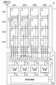
図1は、一実施形態のタッチパネル装置10の構成を概念的に示すブロック図である。タッチパネル装置10は、タッチパネル1とタッチコントローラ2とを備えている。タッチパネル1には、複数の検出電極3が設けられている。本実施形態では、複数の検出電極3は、行列に配置されている。図1の例では、検出電極3が4行4列に配置されているが、検出電極3の数は、様々に変更され得ることに留意されたい。特に、実際の実装では、検出電極3の行及び列の数はより多数(例えば、数十)であり得ることに留意されたい。
FIG. 1 is a block diagram conceptually showing the structure of a
また、本実施形態のタッチパネル装置10は、様々な形態で実装され得ることに留意されたい。実際の実装では、タッチパネル1は、液晶表示パネルと一体化されていてもよい。例えば、液晶表示パネルのアクティブマトリックス基板に画素(画素電極と薄膜トランジスタとを含む)と対向電極とが集積化される場合、当該対向電極が検出電極3として用いられてもよい。この場合、該アクティブマトリックス基板がタッチパネル1としても機能することになる。また、液晶表示パネルの対向基板に行列に配置された複数の対向電極(共通電極とも呼ばれる)が形成される場合には、該対向基板がタッチパネル1として用いられてもよい。この場合、対向基板に形成された該対向電極が、検出電極3として用いられ得る。また、タッチコントローラ2は、独立したIC(integrated circuit)として実装されてもよいし、表示パネル(例えば、液晶表示パネルやOLED(organic light emitting diode)パネル)を駆動する表示ドライバに集積化されてもよい。タッチパネル装置10の具体的な実装の例については後述する。
It should be noted that the
タッチコントローラ2は、タッチパネル1に対して自己容量方式によるタッチ検出を行うように構成されており、複数の外部接続端子4と、セレクタ部5と、センス部6と、演算処理部7とを備えている。
The
外部接続端子4は、検出電極3にそれぞれに接続されている。一の検出電極3に対して一の外部接続端子4が設けられており、各外部接続端子4は、対応する検出電極3にタッチパネル1に形成された配線を介して接続されている。
The
セレクタ部5は、演算処理部7から供給される制御信号SSELに応じて検出電極3とセンス部6との間の接続関係(即ち、外部接続端子4とセンス部6との間の接続関係)を切り換えるように構成されている。本実施形態では、セレクタ部5は、検出電極3の列と同数の、即ち、4つのセレクタ51〜54を備えている。各セレクタ5iは、検出電極3の列と対応しており、対応する列#iの検出電極3(即ち、対応する列の検出電極3に接続されている外部接続端子4)が接続されている。各セレクタ5iは、それに接続されている検出電極3のうちのいずれかを選択し、選択した検出電極3をセンス部6に電気的に接続できるように構成されている。例えば、セレクタ51は、列#1に位置する4つの検出電極3から選択した検出電極3をセンス部6に接続するように構成されており、セレクタ52は、列#2に位置する4つの検出電極3から選択した検出電極3をセンス部6に接続するように構成されている。
The selector unit 5 has a connection relation between the
ここで、本実施形態では、セレクタ51〜54のうちの一部のセレクタが、対応する列と異なる列に位置する検出電極3(即ち、対応する列と異なる列に位置する検出電極3に接続される外部接続端子4)にも接続されている。当該セレクタは、対応する列の検出電極3及び対応する列と異なる列に位置する該検出電極3とのうちのいずれかを選択し、選択した検出電極3をセンス部6に電気的に接続するように構成されている。図1の例では、セレクタ53は、列#3に位置する検出電極3に加えて行#3、列#2に位置する検出電極3に接続されており、列#3に位置する検出電極3と行#3、列#2に位置する検出電極3のうちから選択した検出電極3をセンス部6に接続するように構成されている。また、セレクタ54は、列#4に位置する検出電極3に加えて行#3、列#1に位置する検出電極3に接続されており、列#4に位置する検出電極3と行#3、列#1に位置する検出電極3のうちのいずれかをセンス部6に接続するように構成されている。
Here, in the present embodiment, some of the selectors 5 1 to 5 4 have their
センス部6は、複数のセンス回路61〜64を備えている。本実施形態では、センス回路61〜64の数は、検出電極3の列の数、即ち、セレクタ51〜54の数と同一である。センス回路61〜64は、それぞれ、セレクタ51〜54に接続されている。各センス回路6iに接続される検出電極3は、対応するセレクタ5iによって選択される。言い換えれば、各セレクタ5iは、それぞれに接続されている検出電極3のうちから選択した検出電極3を対応するセンス回路6iに電気的に接続する。各センス回路6iは、対応するセレクタ5iによって選択された検出電極3の自己容量に対応する(自己容量に依存する信号レベルを有する)検出信号を生成する。
The sense unit 6 includes a plurality of sense circuits 6 1 to 6 4 . In the present embodiment, the number of sense circuits 6 1 to 6 4 is the same as the number of columns of the
演算処理部7は、センス部6のセンス回路61〜64によって生成された検出信号に基づいてタッチ検出、即ち、タッチパネル1の人体の指その他の導電体が接触した位置の検出を行う。加えて、演算処理部7は、検出電極3とセンス部6との間の接続関係を制御する制御信号SSELを生成する。制御信号SSELは、タッチパネル装置10の設定及び/又はタッチ検出の結果に応じて生成されてもよい。
The arithmetic processing unit 7 performs touch detection based on the detection signals generated by the sense circuits 6 1 to 6 4 of the sense unit 6, that is, the position where the finger of the human body of the
続いて、本実施形態におけるタッチパネル装置10の動作について説明する。本実施形態のタッチパネル装置10は、表示パネルとタッチパネル1とを備えた表示システム(表示パネルとタッチパネル1とは一体化されていてもよい)に適用される。当該表示システムでは、所定の時間長さ(例えば、16ms)を有する各動作サイクルにおいて、画像を表示する表示動作と、タッチ検出とが行われる。
Next, the operation of the
本実施形態では、各動作サイクルにおけるタッチ検出において、下記の2つの動作:動作#1、#2のうちのいずれかが選択的に行われる。動作#1では、各動作サイクルにおいて、タッチパネル1全面について(即ち、全ての検出電極3について)タッチ検出が行われる。一方、動作#2では、各動作サイクルにおいて、タッチパネル1の一部の領域についてのみ(即ち、一部の検出電極3についてのみ)タッチ検出が行われる。動作#1ではタッチパネル1の全ての検出電極3についてタッチ検出が行われ、動作#2では一部の検出電極3についてのみタッチ検出が行われるのであるから、動作#2においてタッチ検出が行われる検出電極3の数は、動作#1においてタッチ検出が行われる検出電極3の数よりも少ないことに留意されたい。
In the present embodiment, in touch detection in each operation cycle, one of the following two operations:
図2は、タッチ検出において動作#1が行われる場合の表示システムの動作を示すタイミングチャートであり、図3A〜図3Dは、動作#1の各フェーズにおけるタッチパネル装置10の動作を概念的に示すブロック図である。
FIG. 2 is a timing chart showing the operation of the display system when the
図2に図示されるように、本実施形態では、各動作サイクルにおいて、画像を表示する表示動作と、タッチ検出とが交互に行われる。即ち、各動作サイクルは、複数の表示期間と複数のタッチ検出期間を有している。ここで、表示期間とは、表示動作が行われる期間であり、タッチ検出期間とはタッチ検出が行われる期間である。なお、図2の動作では、タッチ検出において動作#1が行われるので、図2においては、タッチ検出の動作が“動作#1”として示されている。
As shown in FIG. 2, in this embodiment, in each operation cycle, a display operation of displaying an image and a touch detection are alternately performed. That is, each operating cycle has a display period and a plurality of touch detection period of several. Here, the display period is a period in which the display operation is performed, and the touch detection period is a period in which the touch detection is performed. Note that in the operation of FIG. 2, the
動作#1は、検出電極3の行の数と同一の数のフェーズを含んでおり、各フェーズにおいては、選択された1行の検出電極3についてのタッチ検出が行われる。ここで、各フェーズにおいては、クロック信号CLKに同期して1行の検出電極3について3回のセンス動作が行われる。1センス動作では、センス回路61〜64により、選択された検出電極3の自己容量に対応する検出信号の取得が1回行われる。
The
タッチパネル装置10(又はタッチコントローラ2)が動作#1を実行する状態(第1状態)に設定されると、各動作サイクルにおいて、検出電極3の行の数と同一の回数の表示動作が行われ、各表示動作の後に動作#1の1フェーズが実施される。本実施形態では、検出電極3の行の数が4であり、動作#1は、4つのフェーズ:PH1〜PH4を含んでいる。フェーズPH1では、行#1に位置する検出電極3についてのタッチ検出が行われ、フェーズPH2では、行#2に位置する検出電極3についてのタッチ検出が行われる。また、フェーズPH3では、行#3に位置する検出電極3についてのタッチ検出が行われ、フェーズPH4では、行#4に位置する検出電極3についてのタッチ検出が行われる。このように、動作#1では、検出電極3の行が順次に選択され、選択された行の検出電極3についてタッチ検出が行われる。よって、タッチパネル1に含まれる全ての検出電極3についてタッチ検出が行われる。
When the touch panel device 10 (or the touch controller 2) is set to the state (first state) in which the
詳細には、図2の動作では、各動作サイクルが開始された後の最初の表示期間において1回目の表示動作が行われ、その後、最初のタッチ検出期間において動作#1のフェーズPH1が行われる。図3Aは、フェーズPH1におけるタッチパネル装置10の動作を示している。フェーズPH1では、制御信号SSELによる制御の下、行#1に位置する検出電極3がセレクタ51〜54によって選択され、それぞれセンス回路61〜64に接続される。図3Aにおいて、セレクタ51〜54によって選択される検出電極3が、ハッチングによって示されていることに留意されたい(図3B〜図3Dについても同様である)。センス回路61〜64は、それぞれに接続された検出電極3の自己容量に対応する検出信号を生成する。検出信号は、自己容量方式において周知である適宜の方法を用いて生成され得る。
Specifically, in the operation of FIG. 2, the first display operation is performed in the first display period after each operation cycle is started, and then the phase PH1 of the
続いて、2番目の表示期間において2回目の表示動作が行われ、その後、2番目のタッチ検出期間において動作#1のフェーズPH2が行われる。図3Bは、フェーズPH2におけるタッチパネル装置10の動作を示している。フェーズPH2では、行#2に位置する検出電極3がセレクタ51〜54によって選択され、それぞれセンス回路61〜64に接続される。センス回路61〜64は、それぞれに接続された検出電極3の自己容量に対応する検出信号を生成する。
Subsequently, the second display operation is performed in the second display period, and then the phase PH2 of the
更に、3番目の表示期間において3回目の表示動作が行われ、その後、3番目のタッチ検出期間において動作#1のフェーズPH3が行われる。図3Cは、フェーズPH3におけるタッチパネル装置10の動作を示している。フェーズPH3では、行#3に位置する検出電極3がセレクタ51〜54によって選択され、それぞれセンス回路61〜64に接続される。センス回路61〜64は、それぞれに接続された検出電極3の自己容量に対応する検出信号を生成する。
Further, the third display operation is performed in the third display period, and then the phase PH3 of the
続いて、4番目の表示期間において4回目の表示動作が行われ、その後、4番目のタッチ検出期間において動作#1のフェーズPH4が行われる。図3Dは、フェーズPH4におけるタッチパネル装置10の動作を示している。フェーズPH4では、行#4に位置する検出電極3がセレクタ51〜54によって選択され、それぞれセンス回路61〜64に接続される。センス回路61〜64は、それぞれに接続された検出電極3の自己容量に対応する検出信号を生成する。
Subsequently, the fourth display operation is performed in the fourth display period, and then the phase PH4 of the
演算処理部7は、検出電極3のそれぞれについて得られた検出信号に基づいてタッチ検出のための演算、即ち、タッチパネル1において導電体(例えば、人体やスタイラス)が接触した位置の検出のための演算を行う。以上の手順により、動作#1では、タッチパネル1の全ての検出電極3についてのタッチ検出、即ち、タッチパネル1の全面についてのタッチ検出が行われる。
The arithmetic processing unit 7 performs an operation for touch detection based on the detection signal obtained for each of the
図4は、タッチ検出において動作#2が行われる場合の表示システムの動作を示すタイミングチャートであり、図5は、動作#2におけるタッチパネル装置10の動作を概念的に示すブロック図である。
FIG. 4 is a timing chart showing the operation of the display system when the
動作#2においては、図5に図示されているように、各動作サイクルにおいて、タッチパネル1の一部の領域(以下、「選択領域8」という。)に位置する検出電極3についてのタッチ検出が行われる。図5の例では、行#3、#4に位置し、列#1、#2に位置する検出電極3についてのタッチ検出が行われる。ここで、図1及び図5から理解されるように、本実施形態では、選択領域8に位置する検出電極3がセレクタ51〜54を介してセンス回路61〜64に電気的に接続可能であることに留意されたい。
In
タッチパネル装置10(又はタッチコントローラ2)が動作#2を実行する状態(第2状態)に設定されると、図4に図示されているように、各動作サイクルにおいて、検出電極3の行の数と同一の回数の表示動作が行われ、更に、各表示動作の後に動作#2が実行される。言い換えれば、各動作サイクルの4つの表示期間のそれぞれにおいて表示動作が行われ、各動作サイクルの4つのタッチ検出期間のそれぞれにおいて選択領域8についてのタッチ検出が行われる。動作#2においては、各動作サイクルにおいて、選択領域8についてのタッチ検出が複数回行われることに留意されたい。これは、選択領域8についてのタッチ検出の感度を高めることができることを意味している。
When the touch panel device 10 (or the touch controller 2) is set to the state (second state) in which the
動作#2では、選択領域8に含まれる検出電極3がセンス回路61〜64に電気的に接続される。詳細には、行#4、列#1に位置する検出電極3がセレクタ51によって選択されてセンス回路61に電気的に接続され、また、行#4、列#2に位置する検出電極3がセレクタ52によって選択されてセンス回路62に電気的に接続される。更に、行#3、列#2に位置する検出電極3がセレクタ53によって選択されてセンス回路63に電気的に接続され、また、行#3、列#1に位置する検出電極3がセレクタ54によって選択されてセンス回路64に電気的に接続される。ここで、セレクタ53が、それが対応する列ではない列に位置する検出電極3をセンス回路63に電気的に接続しており、セレクタ54が、それが対応する列ではない列に位置する検出電極3をセンス回路64に電気的に接続していることに留意されたい。
In
動作#1においては、単一の行に位置する検出電極3が同時にセンス回路61〜64に接続されるが、動作#2においては、複数行に渡って位置する検出電極3が同時にセンス回路61〜64に接続されることに留意されたい。このような動作は、動作#2において列方向に広がった選択領域8を設定可能にする。
Operation In # 1 is detected
センス回路61〜64は、それぞれに接続された検出電極3の自己容量に対応する検出信号を生成する。演算処理部7は、検出電極3のそれぞれについて得られた検出信号に基づいてタッチ検出のための演算、即ち、選択領域8において導電体(例えば、人体やスタイラス)が接触した位置の検出のための演算を行う。以上の手順により、動作#2では、タッチパネル1の選択領域8についてのタッチ検出、即ち、選択領域8に位置する検出電極3についてのタッチ検出が行われる。
The sense circuits 6 1 to 6 4 generate detection signals corresponding to the self-capacitances of the
動作#2では、各動作サイクルにおいて、選択領域8についてのタッチ検出が複数回行われる(即ち、複数のタッチ検出期間のそれぞれについて選択領域8についてのタッチ検出が行われる)ので、選択領域8について高感度でのタッチ検出を行うことができる。この動作#2は、例えば、スタイラスを用いた入力が行われるような場合のように、タッチパネル1の特定の領域について高感度なタッチ検出が求められる場合に有用である。
In
なお、図6に図示されているように、動作#2において、各動作サイクルにおいて選択領域8の各検出電極3についてのタッチ検出が1回のみ行われてもよい。言い換えれば、各動作サイクルの複数のタッチ検出期間のうちの一つのみにおいて選択領域8のついてのタッチ検出が行われてもよい。図6の動作では、1回目の表示動作の後に選択領域8についてのタッチ検出が行われる一方、2回目〜4回目の表示動作の後には、タッチ検出は行われない。この場合には、高感度でのタッチ検出を行うことはできないが、各動作サイクルにおいてタッチ検出が行われる検出電極3の延べ数を少なくできるので、タッチパネル装置10の消費電力を低減することができる。
As shown in FIG. 6, in the
また、上記の動作では、選択領域8に位置する検出電極3の数がセンス回路61〜64の数と同一であり、動作#2においては選択領域8に位置する検出電極3が同時にセンス回路61〜64に接続されるが、選択領域8に位置する検出電極3の数がセンス回路61〜64の数よりも多くてもよい。この場合、動作#2において、選択領域8に位置する検出電極3は、時分割的にセンス回路61〜64に接続される。選択領域8に位置する検出電極3とセンス回路6 1 〜64との対応関係は、タッチコントローラ2の内部における配線(例えば、外部接続端子4とセレクタ51〜54とを接続する配線)を変更することにより、様々に変更可能である。
Further, in the above operation, the number of the
図7は、動作#2において選択領域8に位置する検出電極3が時分割的にセンス回路61〜64に接続されるように構成されたタッチパネル装置10の構成の例を示すブロック図である。図7に図示されているタッチパネル装置10の構成は、図1に図示されているタッチパネル装置10とほぼ同様である。ただし、図7に図示されているタッチパネル装置10では、選択領域8が、列#1、#2に位置する検出電極3を収容するように決定されており、検出電極3とセレクタ51〜54との間の接続関係が、図1に図示されているタッチパネル装置10と異なる。詳細には、図7の例では、セレクタ53は、列#3に位置する検出電極3に加えて行#1、列#2に位置する検出電極3及び行#3、列#2に位置する検出電極3に接続されており、接続されたこれらの検出電極3のうちから選択した検出電極3をセンス部6に電気的に接続するように構成されている。また、セレクタ54は、列#4に位置する検出電極3に加えて行#1、列#1に位置する検出電極3及び行#3、列#1に位置する検出電極3に接続されており、接続されたこれらの検出電極3のうちから選択した検出電極3をセンス部6に電気的に接続するように構成されている。
FIG. 7 is a block diagram showing an example of the configuration of the
図8は、図7に図示されている構成のタッチパネル装置10を含む表示システムにおいて、選択領域8についてタッチ検出を行う場合の動作(動作#2)を示すタイミングチャートであり、図9A、図9Bは、動作#2のフェーズPH1、PH2におけるタッチパネル装置10の動作を概念的に示すブロック図である。なお、図7に図示されている構成のタッチパネル装置10を含む表示システムにおける、タッチパネル1の全面についてタッチ検出を行う場合の動作(動作#1)は、図1に図示されている構成のタッチパネル装置10を含む表示システムと同一である。
Figure 8 is a display system including the
図8の動作では、動作#2は、2つのフェーズPH1、PH2を含んでいる。タッチパネル装置10が動作#2を実行する状態(第2状態)に設定されると、各動作サイクルにおいて、検出電極3の行の数と同一の回数の表示動作が行われ、各表示動作の後に動作#2の1フェーズが実施される。
In the operation of FIG. 8,
詳細には、図8の動作では、各動作サイクルが開始されると、最初の表示期間において1回目の表示動作が行われ、その後、最初のタッチ検出期間において動作#2のフェーズPH1が行われる。図9Aは、フェーズPH1におけるタッチパネル装置10の動作を示している。フェーズPH1では、制御信号SSELによる制御の下、行#2、列#1に位置する検出電極3がセレクタ51によって選択されてセンス回路61に電気的に接続され、また、行#2、列#2に位置する検出電極3がセレクタ52によって選択されてセンス回路62に電気的に接続される。更に、行#1、列#2に位置する検出電極3がセレクタ53によって選択されてセンス回路63に電気的に接続され、また、行#1、列#1に位置する検出電極3がセレクタ54によって選択されてセンス回路64に電気的に接続される。図9A(及び図9B)において、セレクタ51〜54によって選択される検出電極3が、ハッチングによって示されていることに留意されたい。センス回路61〜64は、それぞれに接続された検出電極3の自己容量に対応する検出信号を生成する。検出信号は、自己容量方式において周知である適宜の方法を用いて生成され得る。
Specifically, in the operation of FIG. 8, when each operation cycle is started, the first display operation is performed in the first display period, and then the phase PH1 of
続いて、2番目の表示期間において2回目の表示動作が行われ、その後、2番目のタッチ検出期間において動作#2のフェーズPH2が行われる。図9Bは、フェーズPH2におけるタッチパネル装置10の動作を示している。フェーズPH2では、制御信号SSELによる制御の下、行#4、列#1に位置する検出電極3がセレクタ51によって選択されてセンス回路61に電気的に接続され、また、行#4、列#2に位置する検出電極3がセレクタ52によって選択されてセンス回路62に電気的に接続される。更に、行#3、列#2に位置する検出電極3がセレクタ53によって選択されてセンス回路63に電気的に接続され、また、行#3、列#1に位置する検出電極3がセレクタ54によって選択されてセンス回路64に電気的に接続される。センス回路61〜64は、それぞれに接続された検出電極3の自己容量に対応する検出信号を生成する。
Subsequently, the second display operation is performed in the second display period, and then the phase PH2 of the
更に、3番目の表示期間において3回目の表示動作が行われ、その後、3番目のタッチ検出期間において動作#2のフェーズPH1が再度行われる。更に、4番目の表示期間において4回目の表示動作が行われ、その後、4番目のタッチ検出期間において動作#2のフェーズPH2が再度行われる。図8の動作では、動作#2のフェーズPH1、PH2のそれぞれが、各動作サイクルにおいて2回実行されることになる。
Further, the third display operation is performed in the third display period, and then the phase PH1 of the
演算処理部7は、検出電極3のそれぞれについて得られた検出信号に基づいてタッチ検出のための演算、即ち、選択領域8において導電体(例えば、人体やスタイラス)が接触した位置の検出のための演算を行う。以上の手順により、動作#2では、タッチパネル1の選択領域8についてのタッチ検出、即ち、選択領域8に位置する検出電極3についてのタッチ検出が行われる。
The calculation processing unit 7 performs calculation for touch detection based on the detection signals obtained for each of the
このような動作#2においても、各動作サイクルにおいて、選択領域8の各検出電極3についてのタッチ検出が複数回(図8の動作では、2回)行われるので、選択領域8について高感度でのタッチ検出を行うことができる。
In
また、上記の動作では、選択領域8についてのタッチ検出の動作(動作#2)においてセンス回路61〜64の全てが検出信号の生成に用いられるが、全てのセンス回路61〜64が用いられなくてもよい。選択領域8についてのタッチ検出の動作において、センス回路61〜64の一部のみが使用されてもよい。 In the above operation, all the sense circuit 61 through 4 are used to generate a detection signal in the operation of the touch detection for the selected region 8 (operation # 2), all the sense circuit 61 through 4 May not be used. In the touch detection operation for the selection area 8, only part of the sense circuits 6 1 to 6 4 may be used.
図10は、選択領域8についてのタッチ検出の動作(動作#2)においてセンス回路61〜64の一部のみが使用されるように構成されたタッチパネル装置10の構成の例を示すブロック図である。図10に図示されているタッチパネル装置10の構成は、図1、図7に図示されているタッチパネル装置10とほぼ同様である。ただし、図10に図示されているタッチパネル装置10では、選択領域8が、列#1、#2に位置する検出電極3を収容するように決定されており、検出電極3とセレクタ51〜54との間の接続関係が、図1、図7に図示されているタッチパネル装置10と異なる。
FIG. 10 is a block diagram showing an example of the configuration of the
詳細には、図10の例では、セレクタ53は、列#3に位置する検出電極3に加えて行#3、列#1及び行#3、列#2に位置する検出電極3に接続されており、接続されたこれらの検出電極3のうちから選択した検出電極3をセンス部6に電気的に接続するように構成されている。なお、セレクタ51、52、54は、それぞれ、対応する列#1、2、4に位置する検出電極3に接続されており、接続された検出電極3のうちから選択した検出電極3をセンス部6に電気的に接続するように構成されている。
In particular, in the example of FIG. 10, the selector 5 3,
図11A、図11Bは、選択領域8についてのみタッチ検出を行う場合の動作(動作#2)のフェーズPH1、PH2におけるタッチパネル装置10の動作を概念的に示すブロック図である。なお、図10に図示されている構成のタッチパネル装置10を含む表示システムにおける、タッチパネル1の全面についてのみタッチ検出を行う場合の動作(動作#1)は、図1に図示されている構成のタッチパネル装置10を含む表示システムと同一である。
11A and 11B are block diagrams conceptually showing the operation of the
図10に図示されているタッチパネル装置10の選択領域8についてのみタッチ検出を行う場合の動作(動作#2)は、フェーズPH1、PH2における検出電極3の選択を除けば、図8に図示された動作と同様である。
The operation (operation #2) in the case of performing the touch detection only on the selection area 8 of the
各動作サイクルが開始されると、最初の表示期間において1回目の表示動作が行われ、その後、最初のタッチ検出期間において動作#2のフェーズPH1が行われる。図11Aは、フェーズPH1におけるタッチパネル装置10の動作を示している。フェーズPH1では、制御信号SSELによる制御の下、行#2、列#1に位置する検出電極3がセレクタ51によって選択されてセンス回路61に電気的に接続され、また、行#2、列#2に位置する検出電極3がセレクタ52によって選択されてセンス回路62に電気的に接続される。更に、行#3、列#2に位置する検出電極3がセレクタ53によって選択されてセンス回路63に電気的に接続される。図11A(及び図11B)において、セレクタ51〜5 3 によって選択される検出電極3が、ハッチングによって示されていることに留意されたい。センス回路61〜6 3 は、それぞれに接続された検出電極3の自己容量に対応する検出信号を生成する。検出信号は、自己容量方式において周知である適宜の方法を用いて生成され得る。
When each operation cycle is started, the first display operation is performed in the first display period, and then the phase PH1 of
続いて、2番目の表示期間において2回目の表示動作が行われ、その後、2番目のタッチ検出期間において動作#2のフェーズPH2が行われる。図11Bは、フェーズPH2におけるタッチパネル装置10の動作を示している。フェーズPH2では、制御信号SSELによる制御の下、行#4、列#1に位置する検出電極3がセレクタ51によって選択されてセンス回路61に電気的に接続され、また、行#4、列#2に位置する検出電極3がセレクタ52によって選択されてセンス回路62に電気的に接続される。更に、行#3、列#1に位置する検出電極3がセレクタ53によって選択されてセンス回路63に電気的に接続される。センス回路61〜64は、それぞれに接続された検出電極3の自己容量に対応する検出信号を生成する。
Subsequently, the second display operation is performed in the second display period, and then the phase PH2 of the
更に、3番目の表示期間において3回目の表示動作が行われ、その後、3番目のタッチ検出期間において動作#2のフェーズPH1が再度行われる。更に、4番目の表示期間において4回目の表示動作が行われ、その後、4番目のタッチ検出期間において動作#2のフェーズPH2が再度行われる。上述の動作では、動作#2のフェーズPH1、PH2のそれぞれが、各動作サイクルにおいて2回実行されることになる。
Further, the third display operation is performed in the third display period, and then the phase PH1 of the
演算処理部7は、検出電極3のそれぞれについて得られた検出信号に基づいてタッチ検出のための演算、即ち、選択領域8において導電体(例えば、人体やスタイラス)が接触した位置の検出のための演算を行う。以上の手順により、動作#2では、タッチパネル1の選択領域8についてのタッチ検出、即ち、選択領域8に位置する検出電極3についてのタッチ検出が行われる。
The calculation processing unit 7 performs calculation for touch detection based on the detection signals obtained for each of the
このような動作#2においても、各動作サイクルにおいて、選択領域8の各検出電極3についてのタッチ検出が複数回行われるので、選択領域8について高感度でのタッチ検出を行うことができる。加えて、図11A、図11Bに図示されている動作では、タッチ検出においてセンス回路61〜64の一部しか用いられないため、消費電力を低減することができる。
In
図1、図7、図9のタッチパネル装置10の構成では、選択領域8が、検出電極3とセンス回路61〜64との間の接続関係(即ち、検出電極3(又は外部接続端子4)とセレクタ51〜54との間とを接続する配線のレイアウト)によって固定的に決定されることになる。言い換えれば、図1、図7、図10のタッチパネル装置10の構成では、選択領域8を適宜に変更することが困難である。
In the configuration of the
選択領域8を適宜に変更するためには、検出電極3とセンス部6の各入力との間の接続関係(即ち、検出電極3とセンス回路61〜64との間の接続関係)が、可変に切り替え可能であることが望ましい。図12は、このように構成されたタッチパネル装置10Aの構成を概念的に示すブロック図である。
In order to change the selection region 8 appropriately, the connection relationship between the
図12に図示されたタッチパネル装置10Aのタッチコントローラ2Aでは、図1、図7、図9に図示されているタッチコントローラ2のセレクタ部5とは異なる構成のセレクタ部5Aが用いられる。セレクタ部5Aは、制御信号SSELによる制御の下、タッチパネル1に設けられた任意の検出電極3をセンス部6の任意の入力に(即ち、センス回路61〜64のうちの任意のセンス回路の入力)に電気的に接続することができるように構成されている。
The
詳細には、セレクタ部5Aは、4つのセレクタ5A1〜5A4を備えている。セレクタ5A1〜5A4のそれぞれは、タッチパネル1に設けられた全ての検出電極3に接続されている。セレクタ5A1は、全ての検出電極3のうちから選択した検出電極3をセンス回路61の入力に接続するように構成され、セレクタ5A2は、全ての検出電極3のうちから選択した検出電極3をセンス回路62の入力に接続するように構成されている。同様に、セレクタ5A3は、全ての検出電極3のうちから選択した検出電極3をセンス回路63の入力に接続するように構成され、セレクタ5A4は、全ての検出電極3のうちから選択した検出電極3をセンス回路64の入力に接続するように構成されている。
In detail, the selector unit 5A is provided with four
図12に図示された構成のタッチコントローラ2Aは、任意の組み合わせの検出電極3をセンス回路61〜64に接続可能であり、選択領域8についてのみタッチ検出を行う動作#2において、任意の組み合わせの検出電極3を含む選択領域8を設定可能である。例えば、図5に示されている選択領域8は、動作#2において行#3、列#1に位置する検出電極3、行#3、列#2に位置する検出電極3、行#4、列#1に位置する検出電極3、及び、行#4、列#2に位置する検出電極3を、センス回路61〜64の入力に電気的に接続することで設定することができる。また、図9A、図9Bに示されている選択領域8は、動作#2のフェーズPH1において行#1、列#1に位置する検出電極3、行#1、列#2に位置する検出電極3、行#2、列#1に位置する検出電極3、及び、行#2、列#2に位置する検出電極3をセンス回路61〜64の入力に電気的に接続し、フェーズPH2において行#3、列#1に位置する検出電極3、行#3、列#2に位置する検出電極3、行#4、列#1に位置する検出電極3、及び、行#4、列#2に位置する検出電極3を、センス回路61〜64の入力に電気的に接続することで設定することができる。
続いて、本実施形態のタッチパネル装置(10、10A)の実装の例について説明する。本実施形態のタッチパネル装置は、液晶表示パネルとタッチパネルとが一体化された表示システムに適用され得る。図13は、このような構成の表示システム20の構成の例を示すブロック図である。表示システム20は、液晶表示パネル11と、タッチコントローラ内蔵表示ドライバ12とを備えている。
Next, an example of mounting the touch panel device (10, 10A) of the present embodiment will be described. The touch panel device of this embodiment can be applied to a display system in which a liquid crystal display panel and a touch panel are integrated. FIG. 13 is a block diagram showing an example of the configuration of the
液晶表示パネル11は、アクティブマトリックス基板11aと、対向基板11bとを備えている。アクティブマトリックス基板11aと対向基板11bとは、適宜の空間を挟んで対向しており、当該空間には、液晶が充填される。アクティブマトリックス基板11aには、ソース線と、ゲート線と、TFTで形成された選択トランジスタと、画素電極と、対向電極とが集積化されている。アクティブマトリックス基板11aには、更に、ゲート線を駆動するGIP(gate-in-panel)回路が集積化されていてもよい。
The liquid
図13の表示システム20では、アクティブマトリックス基板11aが、上述の実施形態におけるタッチパネル1としても用いられる。アクティブマトリックス基板11aに設けられた該対向電極が、検出電極3として用いられる。なお、対向基板に対向電極が設けられる場合には、該対向基板に設けられた対向電極が検出電極3として使用されてもよい。
In the
タッチコントローラ内蔵表示ドライバ12は、アクティブマトリックス基板11aに設けられたソース線を駆動して液晶表示パネル11に画像を表示する機能を有すると共に、アクティブマトリックス基板11aに設けられた対向電極を検出電極3として用いてタッチ検出を行う機能も有している。図14は、タッチコントローラ内蔵表示ドライバ12の構成の例を示すブロック図である。タッチコントローラ内蔵表示ドライバ12には、タッチパネル1に設けられた検出電極3(即ち、アクティブマトリックス基板11aに設けられた対向電極)が接続される外部接続端子4と、アクティブマトリックス基板11aに設けられたソース線に接続されるソース出力14とを備えており、更に、タッチコントローラ2とソースドライバ13とが、モノリシックに(monolithically)、即ち、一のチップに集積化されている。タッチコントローラ内蔵表示ドライバ12に集積化されるタッチコントローラ2の構成及び動作は、上述されているとおりである。ソースドライバ13は、アクティブマトリックス基板11aのソース線を駆動する駆動部として動作する。
The
タッチコントローラ内蔵表示ドライバ12は、アクティブマトリックス基板11aに設けられたゲート線を駆動する機能を有していてもよい。また、アクティブマトリックス基板11aにGIP回路が集積化されている場合にはゲート線の駆動を制御する制御信号をGIP回路に供給してもよい。
The
このような構成の表示システム20は、タッチパネル1が液晶表示パネル11に一体化されているため体積を小さくすることができ、加えて、部品数が少ないという利点を有している。このような特徴は、特に携帯端末に搭載される場合に好適である。
The
続いて、本実施形態のタッチパネル装置(10、10A)が、表示パネルとタッチパネルとを備える表示システム(例えば、図13、図14に図示されている表示システム20)に適用される場合の応用例について説明する。図15は、本実施形態のタッチパネル装置(10、10A)が表示システム30に適用された場合の好適な動作の一例を示す概念図である。
Subsequently, an application example in which the touch panel device (10, 10A) of the present embodiment is applied to a display system (for example, the
一実施形態では、図15に図示されているように、タッチパネル1の全面についてのタッチ検出(以下、「全面タッチ検出」ということがある。)と、タッチパネル1の一部分についてのタッチ検出(以下、「部分タッチ検出」ということがある。)とを所定の比率で行ってもよい。部分タッチ検出では、タッチパネル1のうちのタッチ入力領域31のみについてタッチ検出が行われる。タッチ入力領域31とは、ユーザによるタッチ操作を受け付けるための領域である。このような部分タッチ検出は、タッチ入力領域31を上記の選択領域8として選択する、即ち、タッチ入力領域31に設けられた検出電極3についてタッチ検出を行うことで実現できる。
In one embodiment, as illustrated in FIG. 15, touch detection on the entire surface of the touch panel 1 (hereinafter, also referred to as “entire surface touch detection”) and touch detection on a part of the touch panel 1 (hereinafter, referred to as “touch detection”). It may be referred to as “partial touch detection”) at a predetermined ratio. In the partial touch detection, touch detection is performed only on the
タッチ入力領域31について、例えば、スタイラス33によるタッチ操作を受け付けることが意図される場合、タッチ入力領域31についてのタッチ検出を高感度で行うことで、スタイラス33によるタッチ操作をより確実に検出することができる。タッチ入力領域31のタッチ検出を高感度で行う一方で、タッチパネル1のタッチ入力領域31以外の領域についてのタッチ操作を検知可能にするためには、全面タッチ検出を相対的に低頻度で、部分タッチ検出を相対的に高頻度で行うことが望ましい。例えば、N個(Nは、2以上の整数)の動作サイクルにおいてタッチ入力領域31を上記の選択領域8として選択しながら上述の動作#2を行い、更に、1個の動作サイクルにおいて上述の動作#1を行う動作シーケンスを繰り返して行えば、全面タッチ検出を相対的に低頻度で、部分タッチ検出を相対的に高頻度で行うことができる。
For the
このような動作が行われる場合において、タッチ入力領域31へのタッチ操作を反映した画像を表示する領域は、必ずしも、タッチ入力領域31ではなくてもよい。例えば、図16に図示されているように、タッチ入力領域31へのタッチ操作を反映した画像が、タッチパネル1にタッチ入力領域31とは別に定められた画像反映領域32に表示されてもよい。
When such an operation is performed, the area in which the image reflecting the touch operation on the
また、図17に図示されているように、タッチ操作に応じて画像反映領域32を移動させてもよい。例えば、全面タッチ検出によって画像反映領域32に指34による長押しがなされたことを認識した場合(画像反映領域32において長時間、広い面積で導電体が接触していることを検出した場合、このようなタッチ操作がなされたと認識可能である)、システムが、画像反映領域32を移動するモードに遷移する。その後、タッチパネル1に対して行われるタッチ操作が全面タッチ検出によって検出され、検出されたタッチ操作に応じて画像反映領域32が移動される。
Further, as shown in FIG. 17, the
また、図18に図示されているように、タッチ操作に応じてタッチ入力領域31を移動させてもよい。例えば、全面タッチ検出によってタッチ入力領域31に指34による長押しがなされたことを認識した場合、システムが、タッチ入力領域31を移動するモードに遷移する。その後、タッチパネル1に対して行われるタッチ操作が全面タッチ検出によって検出され、検出されたタッチ操作に応じてタッチ入力領域31が移動される。その後においては、移動後のタッチ入力領域31について部分タッチ検出が行われる。タッチパネル1の任意の位置に選択領域8を設定可能である図12のタッチパネル装置10Aの構成によれば、タッチ入力領域31の移動に容易に対応可能である。
Further, as shown in FIG. 18, the
以上には、本発明の実施形態が具体的に記述されているが、本発明は、上記の実施形態に限定されると解釈してはならない。本発明が様々な変更と共に実施され得ることは、当業者には自明的であろう。 Although the embodiments of the present invention have been specifically described above, the present invention should not be construed as being limited to the above embodiments. It will be apparent to those skilled in the art that the present invention can be implemented with various modifications.
1 :タッチパネル
2、2A :タッチコントローラ
3 :検出電極
4 :外部接続端子
5、5A :セレクタ部
51〜54、5A1〜5A4:セレクタ
6 :センス部
61〜64:センス回路
7 :演算処理部
8 :選択領域
10、10A:タッチパネル装置
11 :液晶表示パネル
11a :アクティブマトリックス基板
11b :対向基板
12 :タッチコントローラ内蔵表示ドライバ
13 :ソースドライバ
14 :ソース出力
20 :表示システム
30 :表示システム
31 :タッチ入力領域
32 :画像反映領域
33 :スタイラス
34 :指
1:
Claims (11)
セレクタ部と、
前記複数の検出電極のうちの接続された検出電極の自己容量に依存する信号レベルを有する検出信号を生成するように構成されたセンス部と、
前記検出信号に基づいて前記タッチパネルのタッチ検出を行うように構成された演算処理部
とを備えるタッチパネル装置であって、
前記セレクタ部は、
当該タッチパネル装置が第1状態に設定されると、前記複数の検出電極の行を順次に選択し、選択された行の検出電極を同時に前記センス部に電気的に接続し、
当該タッチパネル装置が第2状態に設定されると、前記複数の検出電極のうちから選択された前記複数の検出電極の数より少ない選択検出電極を前記センス部に電気的に接続するように構成され、
前記セレクタ部が、前記選択検出電極のうち前記複数の検出電極の複数行に渡って位置している検出電極を同時に前記センス部に電気的に接続可能に構成された
タッチパネル装置。 A touch panel having a plurality of detection electrodes arranged in a matrix ,
Selector part,
A sensing unit configured to generate a detection signal having a signal level that depends on the self-capacitance of a connected detection electrode of the plurality of detection electrodes;
A touch panel device and a configured operation processing unit to perform touch detection of the touch panel on the basis of the detection signal,
The selector unit is
When the touch panel device is set to the first state, and select a row of the previous SL plurality of detection electrodes sequentially, electrically connected to the sense portion of the detection electrode of the row selected at the same time,
When the touch panel device is set to the second state, constituting less selective detection electrodes than the number of the plurality of detection electrodes selected from among the previous SL plurality of detecting electrodes so as to be electrically connected to the sense portion Was
The touch panel device , wherein the selector unit is configured to be capable of electrically connecting, at the same time, the detection electrodes of the selected detection electrodes that are located over a plurality of rows of the plurality of detection electrodes to the sense unit .
請求項1に記載のタッチパネル装置。 When those the touch panel device is set to said second state, at each operating cycle, data pitch detection is performed a plurality of times for each of the selected detection electrodes
The touch panel device according to claim 1 .
請求項2に記載のタッチパネル装置。 When those the touch panel device is set to the first state, in each operating cycle, the touch detection is performed once for each of the plurality of detection electrodes
The touch panel device according to claim 2 .
前記複数の検出電極の列にそれぞれに対応する複数のセレクタを備えるセレクタ部と、
前記複数の検出電極のうちの接続された検出電極の自己容量に依存する信号レベルを有する検出信号を生成するように構成されたセンス部と、
前記検出信号に基づいて前記タッチパネルのタッチ検出を行うように構成された演算処理部
とを備えるタッチパネル装置であって、
前記セレクタ部は、
当該タッチパネル装置が第1状態に設定されると、所定の時間長さを有する各動作サイクルにおいて、前記複数の検出電極のうちから選択された第1検出電極を前記センス部に電気的に接続し、
当該タッチパネル装置が第2状態に設定されると、各動作サイクルにおいて、前記複数の検出電極のうちから選択された第2検出電極を前記センス部に電気的に接続するように構成され、
当該タッチパネル装置が前記第2状態に設定されたときに各動作サイクルにおいて前記センス部に接続される前記第2検出電極の数が、当該タッチパネル装置が前記第1状態に設定されたときに各動作サイクルにおいて前記センス部に接続される前記第1検出電極の数よりも少なく、
前記複数のセレクタのそれぞれは、前記複数の検出電極のうちの対応する列の検出電極を選択的に前記センス部に接続可能に構成されており、
前記複数のセレクタの少なくとも一は、前記複数の検出電極のうちの対応する列の検出電極に加え、対応する列以外の列に位置する検出電極を前記センス部に接続可能に構成されている
タッチパネル装置。 A touch panel comprising a plurality of detection electrodes arranged in a matrix,
A selector unit comprising a plurality of selectors corresponding to respective columns of the previous SL plurality of detection electrodes,
A sensing unit configured to generate a detection signal having a signal level that depends on the self-capacitance of a connected detection electrode of the plurality of detection electrodes;
An arithmetic processing unit configured to perform touch detection on the touch panel based on the detection signal.
A touch panel device Ru with bets,
The selector unit is
When the touch panel device is set to the first state, the first detection electrode selected from the plurality of detection electrodes is electrically connected to the sense unit in each operation cycle having a predetermined time length. ,
When the touch panel device is set to the second state, in each operation cycle, a second detection electrode selected from the plurality of detection electrodes is electrically connected to the sense unit,
When the touch panel device is set to the second state, the number of the second detection electrodes connected to the sense unit in each operation cycle is the same as when the touch panel device is set to the first state. Less than the number of the first detection electrodes connected to the sense unit in a cycle,
Each of the plurality of selectors is configured to be able to selectively connect the detection electrodes of a corresponding column of the plurality of detection electrodes to the sense unit,
At least one of the plurality of selectors is configured so that, in addition to the detection electrodes in the corresponding column of the plurality of detection electrodes, the detection electrodes located in columns other than the corresponding column can be connected to the sensing unit. apparatus.
それぞれに接続された検出電極の自己容量に依存する信号レベルを有する検出信号を生成するように構成された複数のセンス回路と、
前記複数の検出電極の全ての検出電極を前記複数のセンス回路のそれぞれに電気的に接続可能に構成されたセレクタ部と、
前記検出信号に基づいて前記タッチパネルのタッチ検出を行うように構成された演算処理部
とを備えるタッチパネル装置であって、
前記セレクタ部は、
当該タッチパネル装置が第1状態に設定されると、所定の時間長さを有する各動作サイクルにおいて、前記複数の検出電極のうちから選択された第1検出電極を前記複数のセンス回路に電気的に接続し、
当該タッチパネル装置が第2状態に設定されると、各動作サイクルにおいて、前記複数の検出電極のうちから選択された第2検出電極を前記複数のセンス回路に電気的に接続するように構成され、
当該タッチパネル装置が前記第2状態に設定されたときに各動作サイクルにおいて前記複数のセンス回路に接続される前記第2検出電極の数が、当該タッチパネル装置が前記第1状態に設定されたときに各動作サイクルにおいて前記複数のセンス回路に接続される前記第1検出電極の数よりも少ない
タッチパネル装置。 A touch panel having a plurality of detection electrodes,
A plurality of sense circuits configured to generate a detection signal having a signal level that depends on the self-capacitance of the detection electrodes connected to each ;
A selector unit which is electrically connectable to the each of the plurality of sense circuits all detection electrodes before Symbol plurality of detection electrodes,
An arithmetic processing unit configured to perform touch detection on the touch panel based on the detection signal.
A touch panel device comprising:
The selector unit is
When the touch panel device is set to the first state, a first detection electrode selected from the plurality of detection electrodes is electrically connected to the plurality of sense circuits in each operation cycle having a predetermined time length. connection,
When the touch panel device is set to the second state, a second detection electrode selected from the plurality of detection electrodes is electrically connected to the plurality of sense circuits in each operation cycle,
When the touch panel device is set to the second state, the number of the second detection electrodes connected to the plurality of sense circuits in each operation cycle is set to the value when the touch panel device is set to the first state. A touch panel device having a smaller number of the first detection electrodes connected to the plurality of sense circuits in each operation cycle .
前記複数のセレクタのそれぞれは、前記複数の検出電極の全てを対応するセンス回路に電気的に接続可能に構成された
請求項5に記載のタッチパネル装置。 Before Symbol selector unit comprises a plurality of selectors corresponding to each of the plurality of sense circuits,
Each of the plurality of selectors is configured to electrically connect all of the plurality of detection electrodes to a corresponding sense circuit.
The touch panel device according to claim 5 .
セレクタ部と、
前記複数の検出電極のうちの接続された検出電極の自己容量に依存する信号レベルを有する検出信号を生成するように構成されたセンス部と、
前記検出信号に基づいて前記タッチパネルのタッチ検出を行うように構成された演算処理部
とを備え、
前記セレクタ部が、
当該タッチコントローラが第1状態に設定されると、前記複数の検出電極の行を順次に選択し、選択された行の検出電極を同時に前記センス部に電気的に接続し、
当該タッチコントローラが第2状態に設定されると、前記複数の検出電極のうちから選択された前記複数の検出電極の数よりも少ない選択検出電極を前記センス部に電気的に接続するように構成され、
前記セレクタ部が、前記選択検出電極のうち前記複数の検出電極の複数行に渡って位置している検出電極を同時に前記センス部に電気的に接続可能に構成された
タッチコントローラ。 A touch controller for performing touch detection on a touch panel having a plurality of detection electrodes arranged in a matrix ,
And the selector section,
A sensing unit configured to generate a detection signal having a signal level that is dependent on the self-capacitance of a connected detection electrode of the plurality of detection electrodes;
An arithmetic processing unit configured to perform touch detection of the touch panel based on the detection signal ,
The selector section is
When the touch controller is set to the first state, before Symbol sequentially selects the rows of the detection electrodes, electrically connected to the sense unit sensing electrodes of rows simultaneously selected,
When the touch controller is set to the second state, the less selective detection electrodes than the number of the plurality of detection electrodes selected from among the previous SL plurality of detecting electrodes so as to be electrically connected to the sense portion Composed,
The touch controller , wherein the selector unit is configured to be capable of electrically connecting the detection electrodes of the selected detection electrodes, which are located over a plurality of rows of the plurality of detection electrodes, to the sense unit at the same time .
前記複数の検出電極の列にそれぞれに対応する複数のセレクタを備えるセレクタ部と、
前記複数の検出電極のうちの接続された検出電極の自己容量に依存する信号レベルを有する検出信号を生成するように構成されたセンス部と、
前記検出信号に基づいて前記タッチパネルのタッチ検出を行うように構成された演算処理部
とを備え、
前記セレクタ部は、
当該タッチコントローラが第1状態に設定されると、所定の時間長さを有する各動作サイクルにおいて、前記複数の検出電極のうちから選択された第1検出電極を前記センス部に電気的に接続し、
当該タッチコントローラが第2状態に設定されると、各動作サイクルにおいて、前記複数の検出電極のうちから選択された第2検出電極を前記センス部に電気的に接続するように構成され、
当該タッチコントローラが前記第2状態に設定されたときに各動作サイクルにおいて前記センス部に接続される前記第2検出電極の数が、当該タッチコントローラが前記第1状態に設定されたときに各動作サイクルにおいて前記センス部に接続される前記第1検出電極の数よりも少なく、
前記複数のセレクタのそれぞれは、前記複数の検出電極のうちの対応する列の検出電極を選択的に前記センス部に接続可能に構成されており、
前記複数のセレクタの少なくとも一は、前記複数の検出電極のうちの対応する列の検出電極に加え、対応する列以外の列に位置する検出電極を前記センス部に接続可能に構成されている
タッチコントローラ。 A touch controller for performing touch detection on a touch panel having a plurality of detection electrodes arranged in a matrix ,
A selector unit comprising a plurality of selectors corresponding to respective columns of the previous SL plurality of detection electrodes,
A sensing unit configured to generate a detection signal having a signal level that depends on the self-capacitance of a connected detection electrode of the plurality of detection electrodes;
An arithmetic processing unit configured to perform touch detection on the touch panel based on the detection signal.
With and
The selector unit is
When the touch controller is set to the first state, the first detection electrode selected from the plurality of detection electrodes is electrically connected to the sense unit in each operation cycle having a predetermined time length. ,
When the touch controller is set to the second state, it is configured to electrically connect the second detection electrode selected from the plurality of detection electrodes to the sense unit in each operation cycle,
When the touch controller is set to the second state, the number of the second detection electrodes connected to the sense unit in each operation cycle is equal to each operation when the touch controller is set to the first state. Less than the number of the first detection electrodes connected to the sense unit in a cycle,
Each of the plurality of selectors is configured to be able to selectively connect the detection electrodes of a corresponding column of the plurality of detection electrodes to the sense unit,
At least one of the plurality of selectors is configured so that, in addition to the detection electrodes in the corresponding column of the plurality of detection electrodes, the detection electrodes located in columns other than the corresponding column can be connected to the sense unit. controller.
それぞれに接続された検出電極の自己容量に依存する信号レベルを有する検出信号を生成するように構成された複数のセンス回路と、
前記複数の検出電極の全ての検出電極を前記複数のセンス回路のそれぞれに電気的に接続可能に構成されたセレクタ部と、
前記検出信号に基づいて前記タッチパネルのタッチ検出を行うように構成された演算処理部
とを備え、
前記セレクタ部は、
当該タッチコントローラが第1状態に設定されると、所定の時間長さを有する各動作サイクルにおいて、前記複数の検出電極のうちから選択された第1検出電極を前記複数のセンス回路に電気的に接続し、
当該タッチコントローラが第2状態に設定されると、各動作サイクルにおいて、前記複数の検出電極のうちから選択された第2検出電極を前記複数のセンス回路に電気的に接続するように構成され、
当該タッチコントローラが前記第2状態に設定されたときに各動作サイクルにおいて前記複数のセンス回路に接続される前記第2検出電極の数が、当該タッチコントローラが前記第1状態に設定されたときに各動作サイクルにおいて前記複数のセンス回路に接続される前記第1検出電極の数よりも少ない
タッチコントローラ。 A data pitch controller for touch detection on the touch panel having a plurality of detection electrodes,
A plurality of sense circuits configured to generate a detection signal having a signal level that depends on the self-capacitance of the detection electrodes connected to each ;
A selector unit which is electrically connectable to the each of the plurality of sense circuits all detection electrodes before Symbol plurality of detection electrodes,
An arithmetic processing unit configured to perform touch detection on the touch panel based on the detection signal.
With and
The selector unit is
When the touch controller is set to the first state, a first detection electrode selected from the plurality of detection electrodes is electrically connected to the plurality of sense circuits in each operation cycle having a predetermined time length. connection,
When the touch controller is set to the second state, in each operation cycle, a second detection electrode selected from the plurality of detection electrodes is electrically connected to the plurality of sense circuits,
When the touch controller is set to the second state, the number of the second detection electrodes connected to the plurality of sense circuits in each operation cycle is set when the touch controller is set to the first state. A touch controller having less than the number of the first detection electrodes connected to the plurality of sense circuits in each operation cycle .
所定の時間長さを有する各動作サイクルにおいて第1動作と第2動作のうちから選択された動作を行うステップを具備し、
前記第1動作は、
前記複数の検出電極のうちから選択された行を順次に選択し、選択された行の検出電極を同時にセンス部に電気的に接続することと、
前記センス部により、前記選択された行の前記検出電極の自己容量に依存する信号レベルを有する第1検出信号を生成することと、
生成された前記第1検出信号に基づいて前記複数の検出電極についてタッチ検出を行うこと
とを含み、
前記第2動作は、
前記複数の検出電極のうちから選択された前記複数の検出電極の数より少ない選択検出電極を前記センス部に電気的に接続することと、
前記センス部により、前記センス部に電気的に接続された前記選択検出電極の自己容量に依存する信号レベルを有する第2検出信号を生成することと、
生成された前記第2検出信号に基づいて前記選択検出電極についてタッチ検出を行うこと
とを含み、
前記選択検出電極を前記センス部に電気的に接続することは、前記選択検出電極のうち前記複数の検出電極の複数行に渡って位置している検出電極を同時に前記センス部に電気的に接続することを含む
タッチ検出方法。 In a touch panel device including a touch panel having a plurality of detection electrodes, a touch detection method for performing touch detection on the touch panel,
A step of performing an operation selected from a first operation and a second operation in each operation cycle having a predetermined time length,
The first operation is
And that the previous SL sequentially selects the selected row from among the plurality of detection electrodes, electrically connected to a sense unit sensing electrodes of rows simultaneously selected,
And said by the sense unit, to generate a first detection signal having a signal level that depends on the self-capacitance of the pre-Symbol detection electrode of the selected row,
Based on the generated first detecting signal and a <br/> to perform touch detection on the plurality of detection electrodes,
The second operation is
And be electrically connected to the sense unit less selective detection electrodes than the number of the plurality of detection electrodes selected from among the previous SL plurality of detection electrodes,
And that by the sense unit, generates a second detection signal having a signal level that depends on the self-capacitance of which is electrically connected to said selected detection electrodes to the sense unit,
And a <br/> to perform touch detection on the selected detection electrodes on the basis of the generated second detection signal,
Electrically connecting the selection detection electrode to the sense unit means electrically connecting the detection electrodes located in a plurality of rows of the plurality of detection electrodes among the selection detection electrodes to the sense unit at the same time. A touch detection method including :
請求項10に記載のタッチ検出方法。
Higher than the frequency of the frequency of pre-Symbol second operation is performed, the first operation is performed
The touch detection method according to claim 10 .
Priority Applications (3)
| Application Number | Priority Date | Filing Date | Title |
|---|---|---|---|
| JP2016025948A JP6706508B2 (en) | 2016-02-15 | 2016-02-15 | Touch panel device, touch controller, and touch detection method |
| US15/425,150 US10222916B2 (en) | 2016-02-15 | 2017-02-06 | Device and method for self-capacitance touch sensing |
| CN201710080932.5A CN107085486A (en) | 2016-02-15 | 2017-02-15 | Touch-panel device, touch controller and touch detecting method |
Applications Claiming Priority (1)
| Application Number | Priority Date | Filing Date | Title |
|---|---|---|---|
| JP2016025948A JP6706508B2 (en) | 2016-02-15 | 2016-02-15 | Touch panel device, touch controller, and touch detection method |
Publications (3)
| Publication Number | Publication Date |
|---|---|
| JP2017146660A JP2017146660A (en) | 2017-08-24 |
| JP2017146660A5 JP2017146660A5 (en) | 2019-03-28 |
| JP6706508B2 true JP6706508B2 (en) | 2020-06-10 |
Family
ID=59562072
Family Applications (1)
| Application Number | Title | Priority Date | Filing Date |
|---|---|---|---|
| JP2016025948A Active JP6706508B2 (en) | 2016-02-15 | 2016-02-15 | Touch panel device, touch controller, and touch detection method |
Country Status (3)
| Country | Link |
|---|---|
| US (1) | US10222916B2 (en) |
| JP (1) | JP6706508B2 (en) |
| CN (1) | CN107085486A (en) |
Families Citing this family (8)
| Publication number | Priority date | Publication date | Assignee | Title |
|---|---|---|---|---|
| KR102539856B1 (en) * | 2016-07-28 | 2023-06-08 | 엘지디스플레이 주식회사 | Display and gate driving circuit thereof |
| CN107908303B (en) * | 2016-10-04 | 2021-02-12 | 禾瑞亚科技股份有限公司 | Touch processing device, electronic system and touch processing method thereof |
| CN107562280B (en) * | 2017-09-15 | 2021-04-09 | 京东方科技集团股份有限公司 | Pressure touch display device and manufacturing and driving method |
| CN109871146B (en) * | 2019-02-21 | 2022-05-27 | 北京集创北方科技股份有限公司 | Touch device and information processing equipment |
| CN111752420B (en) * | 2019-03-27 | 2024-04-30 | 松下汽车电子系统株式会社 | Display system, control device, control method and display device |
| JP7373797B2 (en) * | 2019-03-27 | 2023-11-06 | パナソニックIpマネジメント株式会社 | Display system, control device, control method and display device |
| KR20220021326A (en) | 2020-08-13 | 2022-02-22 | 삼성전자주식회사 | Apparatus and method for sensing touch based on multi-channel |
| JP2023117040A (en) * | 2022-02-10 | 2023-08-23 | 株式会社ジャパンディスプレイ | Detection device, and driving method of detection device |
Family Cites Families (13)
| Publication number | Priority date | Publication date | Assignee | Title |
|---|---|---|---|---|
| JP3193811B2 (en) * | 1993-09-09 | 2001-07-30 | シャープ株式会社 | Display integrated tablet device |
| JP2007084723A (en) * | 2005-09-22 | 2007-04-05 | Kasei Optonix Co Ltd | Red light-emitting phosphor for low-velocity electron beam, red light-emitting composition and fluorescent display using the same |
| JP2011242908A (en) * | 2010-05-17 | 2011-12-01 | Panasonic Corp | Touch panel device and touch panel system comprising the same |
| CN102254458B (en) * | 2010-05-21 | 2013-01-09 | 汉王科技股份有限公司 | Method for strobing antenna array of electromagnetic type ebook reader |
| JP2012103797A (en) * | 2010-11-08 | 2012-05-31 | Sony Corp | Input device, coordinate detection method and program |
| TWI590133B (en) * | 2010-12-31 | 2017-07-01 | 樂金顯示科技股份有限公司 | Apparatus and method for driving touch sensor |
| JP6012437B2 (en) | 2012-11-29 | 2016-10-25 | シナプティクス・ジャパン合同会社 | Semiconductor device and electronic equipment |
| JP6045924B2 (en) * | 2013-01-28 | 2016-12-14 | シナプティクス・ジャパン合同会社 | Touch panel display device and touch panel controller |
| JP6216145B2 (en) | 2013-04-22 | 2017-10-18 | シナプティクス・ジャパン合同会社 | Touch panel controller and semiconductor device |
| US9298299B2 (en) * | 2013-10-02 | 2016-03-29 | Synaptics Incorporated | Multi-sensor touch integrated display driver configuration for capacitive sensing devices |
| US9817513B2 (en) * | 2015-01-27 | 2017-11-14 | Apple Inc. | Sense amplifier stabilization with switched series resistor |
| AU2016215616B2 (en) * | 2015-02-02 | 2018-12-06 | Apple Inc. | Flexible self-capacitance and mutual capacitance touch sensing system architecture |
| US10365773B2 (en) * | 2015-09-30 | 2019-07-30 | Apple Inc. | Flexible scan plan using coarse mutual capacitance and fully-guarded measurements |
-
2016
- 2016-02-15 JP JP2016025948A patent/JP6706508B2/en active Active
-
2017
- 2017-02-06 US US15/425,150 patent/US10222916B2/en active Active
- 2017-02-15 CN CN201710080932.5A patent/CN107085486A/en active Pending
Also Published As
| Publication number | Publication date |
|---|---|
| CN107085486A (en) | 2017-08-22 |
| US20170235392A1 (en) | 2017-08-17 |
| US10222916B2 (en) | 2019-03-05 |
| JP2017146660A (en) | 2017-08-24 |
Similar Documents
| Publication | Publication Date | Title |
|---|---|---|
| JP6706508B2 (en) | Touch panel device, touch controller, and touch detection method | |
| JP6045924B2 (en) | Touch panel display device and touch panel controller | |
| CN107967893B (en) | Intracellular touch organic light-emitting display device and driving circuit thereof | |
| JP6216145B2 (en) | Touch panel controller and semiconductor device | |
| US8970527B2 (en) | Capacitive touch panel having mutual capacitance and self capacitance sensing modes and sensing method thereof | |
| US9904407B2 (en) | Touch sensor, display apparatus including the same, and method of sensing touch panel | |
| WO2018192453A1 (en) | Touch control drive method and apparatus, switching method, touch control apparatus, and electronic device | |
| KR102133736B1 (en) | Display device with integrated touch screen and method for driving the same | |
| US10001877B2 (en) | Semiconductor device | |
| JP2007172028A (en) | Input device | |
| EP3719621B1 (en) | Touch panel, touch device, and method for manufacturing touch panel | |
| KR20140023567A (en) | Display device with integrated touch screen and method for driving the same | |
| US10824267B2 (en) | Input detection device, electronic device and display device | |
| JP2017146660A5 (en) | ||
| WO2016070524A1 (en) | Embedded touch screen, display apparatus and touch drive method | |
| JP2005352572A (en) | Coordinate input device | |
| US20140225844A1 (en) | Display device and touch panel | |
| KR102321247B1 (en) | Apparatus for improving signal-to-noise performance of projected capacitance touch screens and panels | |
| JP4633536B2 (en) | Display device | |
| KR20190048861A (en) | Display device and driving method thereof | |
| US10691247B2 (en) | Display panel having pressure detecting in gate driving circuit and electronic device thereof | |
| KR102171623B1 (en) | Touch screen having minmal touch sensor control signal and display apparatus and touch scan method of touch screen | |
| KR20220012664A (en) | Touch display device, touch circuit, and touch driving method thereof | |
| KR20160115644A (en) | Driver integrated circuit, driving method, and touch display system | |
| CN114385037B (en) | Touch display panel and touch display device |
Legal Events
| Date | Code | Title | Description |
|---|---|---|---|
| RD04 | Notification of resignation of power of attorney |
Free format text: JAPANESE INTERMEDIATE CODE: A7424 Effective date: 20160825 |
|
| A521 | Request for written amendment filed |
Free format text: JAPANESE INTERMEDIATE CODE: A523 Effective date: 20190208 |
|
| A621 | Written request for application examination |
Free format text: JAPANESE INTERMEDIATE CODE: A621 Effective date: 20190208 |
|
| RD03 | Notification of appointment of power of attorney |
Free format text: JAPANESE INTERMEDIATE CODE: A7423 Effective date: 20190208 |
|
| A977 | Report on retrieval |
Free format text: JAPANESE INTERMEDIATE CODE: A971007 Effective date: 20190911 |
|
| A131 | Notification of reasons for refusal |
Free format text: JAPANESE INTERMEDIATE CODE: A131 Effective date: 20191009 |
|
| RD04 | Notification of resignation of power of attorney |
Free format text: JAPANESE INTERMEDIATE CODE: A7424 Effective date: 20191122 |
|
| A521 | Request for written amendment filed |
Free format text: JAPANESE INTERMEDIATE CODE: A523 Effective date: 20191205 |
|
| TRDD | Decision of grant or rejection written | ||
| A01 | Written decision to grant a patent or to grant a registration (utility model) |
Free format text: JAPANESE INTERMEDIATE CODE: A01 Effective date: 20200428 |
|
| A61 | First payment of annual fees (during grant procedure) |
Free format text: JAPANESE INTERMEDIATE CODE: A61 Effective date: 20200518 |
|
| R150 | Certificate of patent or registration of utility model |
Ref document number: 6706508 Country of ref document: JP Free format text: JAPANESE INTERMEDIATE CODE: R150 |
|
| R250 | Receipt of annual fees |
Free format text: JAPANESE INTERMEDIATE CODE: R250 |
|
| R250 | Receipt of annual fees |
Free format text: JAPANESE INTERMEDIATE CODE: R250 |
|
| S111 | Request for change of ownership or part of ownership |
Free format text: JAPANESE INTERMEDIATE CODE: R313113 |
|
| R360 | Written notification for declining of transfer of rights |
Free format text: JAPANESE INTERMEDIATE CODE: R360 |
|
| R360 | Written notification for declining of transfer of rights |
Free format text: JAPANESE INTERMEDIATE CODE: R360 |
|
| R371 | Transfer withdrawn |
Free format text: JAPANESE INTERMEDIATE CODE: R371 |
|
| S111 | Request for change of ownership or part of ownership |
Free format text: JAPANESE INTERMEDIATE CODE: R313113 |