JP6697406B2 - Transparent electrode, electronic device, and method for manufacturing electronic device - Google Patents
Transparent electrode, electronic device, and method for manufacturing electronic device Download PDFInfo
- Publication number
- JP6697406B2 JP6697406B2 JP2017009700A JP2017009700A JP6697406B2 JP 6697406 B2 JP6697406 B2 JP 6697406B2 JP 2017009700 A JP2017009700 A JP 2017009700A JP 2017009700 A JP2017009700 A JP 2017009700A JP 6697406 B2 JP6697406 B2 JP 6697406B2
- Authority
- JP
- Japan
- Prior art keywords
- layer
- film
- graphene
- electronic device
- photoelectric conversion
- Prior art date
- Legal status (The legal status is an assumption and is not a legal conclusion. Google has not performed a legal analysis and makes no representation as to the accuracy of the status listed.)
- Active
Links
- 238000000034 method Methods 0.000 title claims description 31
- 238000004519 manufacturing process Methods 0.000 title claims description 12
- 229910021389 graphene Inorganic materials 0.000 claims description 151
- 238000006243 chemical reaction Methods 0.000 claims description 109
- OKTJSMMVPCPJKN-UHFFFAOYSA-N Carbon Chemical compound [C] OKTJSMMVPCPJKN-UHFFFAOYSA-N 0.000 claims description 68
- 229920001940 conductive polymer Polymers 0.000 claims description 36
- 239000007848 Bronsted acid Substances 0.000 claims description 33
- 150000001450 anions Chemical class 0.000 claims description 29
- 150000001768 cations Chemical class 0.000 claims description 28
- 229910001316 Ag alloy Inorganic materials 0.000 claims description 26
- 229910052751 metal Inorganic materials 0.000 claims description 25
- 239000002184 metal Substances 0.000 claims description 25
- 125000004433 nitrogen atom Chemical group N* 0.000 claims description 24
- 229910052809 inorganic oxide Inorganic materials 0.000 claims description 21
- -1 polyol compound Chemical class 0.000 claims description 20
- 239000000758 substrate Substances 0.000 claims description 19
- 125000004432 carbon atom Chemical group C* 0.000 claims description 12
- 229910052757 nitrogen Inorganic materials 0.000 claims description 12
- BQCADISMDOOEFD-UHFFFAOYSA-N Silver Chemical compound [Ag] BQCADISMDOOEFD-UHFFFAOYSA-N 0.000 claims description 9
- 229910052709 silver Inorganic materials 0.000 claims description 9
- 239000004332 silver Substances 0.000 claims description 9
- 229910052799 carbon Inorganic materials 0.000 claims description 7
- 239000013078 crystal Substances 0.000 claims description 6
- 229920005862 polyol Polymers 0.000 claims description 5
- 125000004429 atom Chemical group 0.000 claims description 3
- 125000005843 halogen group Chemical group 0.000 claims 2
- 239000010410 layer Substances 0.000 description 366
- 239000010408 film Substances 0.000 description 154
- 239000000872 buffer Substances 0.000 description 57
- 239000000243 solution Substances 0.000 description 34
- 229920000642 polymer Polymers 0.000 description 32
- 229920002799 BoPET Polymers 0.000 description 29
- 239000007864 aqueous solution Substances 0.000 description 29
- GWEVSGVZZGPLCZ-UHFFFAOYSA-N Titan oxide Chemical compound O=[Ti]=O GWEVSGVZZGPLCZ-UHFFFAOYSA-N 0.000 description 28
- XKRFYHLGVUSROY-UHFFFAOYSA-N Argon Chemical compound [Ar] XKRFYHLGVUSROY-UHFFFAOYSA-N 0.000 description 26
- 238000012546 transfer Methods 0.000 description 24
- 229920001609 Poly(3,4-ethylenedioxythiophene) Polymers 0.000 description 22
- 239000002356 single layer Substances 0.000 description 22
- OAKJQQAXSVQMHS-UHFFFAOYSA-N Hydrazine Chemical compound NN OAKJQQAXSVQMHS-UHFFFAOYSA-N 0.000 description 20
- 238000001035 drying Methods 0.000 description 20
- QGZKDVFQNNGYKY-UHFFFAOYSA-N Ammonia Chemical compound N QGZKDVFQNNGYKY-UHFFFAOYSA-N 0.000 description 19
- 230000006866 deterioration Effects 0.000 description 19
- KFZMGEQAYNKOFK-UHFFFAOYSA-N Isopropanol Chemical compound CC(C)O KFZMGEQAYNKOFK-UHFFFAOYSA-N 0.000 description 18
- ZMXDDKWLCZADIW-UHFFFAOYSA-N N,N-Dimethylformamide Chemical compound CN(C)C=O ZMXDDKWLCZADIW-UHFFFAOYSA-N 0.000 description 18
- 229920006254 polymer film Polymers 0.000 description 17
- 239000010409 thin film Substances 0.000 description 17
- OGIDPMRJRNCKJF-UHFFFAOYSA-N titanium oxide Inorganic materials [Ti]=O OGIDPMRJRNCKJF-UHFFFAOYSA-N 0.000 description 17
- IJGRMHOSHXDMSA-UHFFFAOYSA-N Atomic nitrogen Chemical compound N#N IJGRMHOSHXDMSA-UHFFFAOYSA-N 0.000 description 15
- YXFVVABEGXRONW-UHFFFAOYSA-N Toluene Chemical compound CC1=CC=CC=C1 YXFVVABEGXRONW-UHFFFAOYSA-N 0.000 description 15
- RYGMFSIKBFXOCR-UHFFFAOYSA-N Copper Chemical compound [Cu] RYGMFSIKBFXOCR-UHFFFAOYSA-N 0.000 description 14
- 230000008859 change Effects 0.000 description 14
- 239000004065 semiconductor Substances 0.000 description 14
- 229910052786 argon Inorganic materials 0.000 description 13
- VEXZGXHMUGYJMC-UHFFFAOYSA-N Hydrochloric acid Chemical compound Cl VEXZGXHMUGYJMC-UHFFFAOYSA-N 0.000 description 12
- BAVYZALUXZFZLV-UHFFFAOYSA-N Methylamine Chemical compound NC BAVYZALUXZFZLV-UHFFFAOYSA-N 0.000 description 12
- XLOMVQKBTHCTTD-UHFFFAOYSA-N Zinc monoxide Chemical compound [Zn]=O XLOMVQKBTHCTTD-UHFFFAOYSA-N 0.000 description 12
- VNWKTOKETHGBQD-UHFFFAOYSA-N methane Chemical compound C VNWKTOKETHGBQD-UHFFFAOYSA-N 0.000 description 12
- 239000002253 acid Substances 0.000 description 11
- 229910052736 halogen Inorganic materials 0.000 description 10
- 229910021529 ammonia Inorganic materials 0.000 description 9
- 239000010949 copper Substances 0.000 description 9
- 239000006185 dispersion Substances 0.000 description 9
- 229920000123 polythiophene Polymers 0.000 description 9
- 238000004544 sputter deposition Methods 0.000 description 9
- 238000000026 X-ray photoelectron spectrum Methods 0.000 description 8
- 238000010586 diagram Methods 0.000 description 8
- 238000009792 diffusion process Methods 0.000 description 8
- 230000000694 effects Effects 0.000 description 8
- 239000012298 atmosphere Substances 0.000 description 7
- 238000000576 coating method Methods 0.000 description 7
- CBENFWSGALASAD-UHFFFAOYSA-N Ozone Chemical compound [O-][O+]=O CBENFWSGALASAD-UHFFFAOYSA-N 0.000 description 6
- 239000002585 base Substances 0.000 description 6
- 239000011248 coating agent Substances 0.000 description 6
- 229910052802 copper Inorganic materials 0.000 description 6
- ORTQZVOHEJQUHG-UHFFFAOYSA-L copper(II) chloride Chemical compound Cl[Cu]Cl ORTQZVOHEJQUHG-UHFFFAOYSA-L 0.000 description 6
- 239000011888 foil Substances 0.000 description 6
- 238000010438 heat treatment Methods 0.000 description 6
- 239000001257 hydrogen Substances 0.000 description 6
- 229910052739 hydrogen Inorganic materials 0.000 description 6
- 239000007788 liquid Substances 0.000 description 6
- 239000000463 material Substances 0.000 description 6
- 239000002105 nanoparticle Substances 0.000 description 6
- 229910001220 stainless steel Inorganic materials 0.000 description 6
- 239000010935 stainless steel Substances 0.000 description 6
- XLYOFNOQVPJJNP-UHFFFAOYSA-N water Substances O XLYOFNOQVPJJNP-UHFFFAOYSA-N 0.000 description 6
- 239000011787 zinc oxide Substances 0.000 description 6
- LFQSCWFLJHTTHZ-UHFFFAOYSA-N Ethanol Chemical compound CCO LFQSCWFLJHTTHZ-UHFFFAOYSA-N 0.000 description 5
- ATJFFYVFTNAWJD-UHFFFAOYSA-N Tin Chemical compound [Sn] ATJFFYVFTNAWJD-UHFFFAOYSA-N 0.000 description 5
- 238000005229 chemical vapour deposition Methods 0.000 description 5
- 150000001875 compounds Chemical class 0.000 description 5
- 125000004435 hydrogen atom Chemical class [H]* 0.000 description 5
- 238000002347 injection Methods 0.000 description 5
- 239000007924 injection Substances 0.000 description 5
- 238000005304 joining Methods 0.000 description 5
- 238000010030 laminating Methods 0.000 description 5
- 150000003839 salts Chemical class 0.000 description 5
- 229910052718 tin Inorganic materials 0.000 description 5
- 125000000217 alkyl group Chemical group 0.000 description 4
- 239000003054 catalyst Substances 0.000 description 4
- 239000011889 copper foil Substances 0.000 description 4
- 230000007423 decrease Effects 0.000 description 4
- GNTDGMZSJNCJKK-UHFFFAOYSA-N divanadium pentaoxide Chemical compound O=[V](=O)O[V](=O)=O GNTDGMZSJNCJKK-UHFFFAOYSA-N 0.000 description 4
- 150000002367 halogens Chemical class 0.000 description 4
- 229910052738 indium Inorganic materials 0.000 description 4
- APFVFJFRJDLVQX-UHFFFAOYSA-N indium atom Chemical compound [In] APFVFJFRJDLVQX-UHFFFAOYSA-N 0.000 description 4
- JKQOBWVOAYFWKG-UHFFFAOYSA-N molybdenum trioxide Chemical compound O=[Mo](=O)=O JKQOBWVOAYFWKG-UHFFFAOYSA-N 0.000 description 4
- 230000003287 optical effect Effects 0.000 description 4
- 239000002245 particle Substances 0.000 description 4
- 229920000139 polyethylene terephthalate Polymers 0.000 description 4
- 239000005020 polyethylene terephthalate Substances 0.000 description 4
- RPAJSBKBKSSMLJ-DFWYDOINSA-N (2s)-2-aminopentanedioic acid;hydrochloride Chemical class Cl.OC(=O)[C@@H](N)CCC(O)=O RPAJSBKBKSSMLJ-DFWYDOINSA-N 0.000 description 3
- XDXWNHPWWKGTKO-UHFFFAOYSA-N 207739-72-8 Chemical compound C1=CC(OC)=CC=C1N(C=1C=C2C3(C4=CC(=CC=C4C2=CC=1)N(C=1C=CC(OC)=CC=1)C=1C=CC(OC)=CC=1)C1=CC(=CC=C1C1=CC=C(C=C13)N(C=1C=CC(OC)=CC=1)C=1C=CC(OC)=CC=1)N(C=1C=CC(OC)=CC=1)C=1C=CC(OC)=CC=1)C1=CC=C(OC)C=C1 XDXWNHPWWKGTKO-UHFFFAOYSA-N 0.000 description 3
- OKKJLVBELUTLKV-UHFFFAOYSA-N Methanol Chemical compound OC OKKJLVBELUTLKV-UHFFFAOYSA-N 0.000 description 3
- LRHPLDYGYMQRHN-UHFFFAOYSA-N N-Butanol Chemical compound CCCCO LRHPLDYGYMQRHN-UHFFFAOYSA-N 0.000 description 3
- PXHVJJICTQNCMI-UHFFFAOYSA-N Nickel Chemical compound [Ni] PXHVJJICTQNCMI-UHFFFAOYSA-N 0.000 description 3
- VYPSYNLAJGMNEJ-UHFFFAOYSA-N Silicium dioxide Chemical compound O=[Si]=O VYPSYNLAJGMNEJ-UHFFFAOYSA-N 0.000 description 3
- HEMHJVSKTPXQMS-UHFFFAOYSA-M Sodium hydroxide Chemical compound [OH-].[Na+] HEMHJVSKTPXQMS-UHFFFAOYSA-M 0.000 description 3
- 239000003575 carbonaceous material Substances 0.000 description 3
- 230000000052 comparative effect Effects 0.000 description 3
- 229960003280 cupric chloride Drugs 0.000 description 3
- 239000007789 gas Substances 0.000 description 3
- PQXKHYXIUOZZFA-UHFFFAOYSA-M lithium fluoride Chemical compound [Li+].[F-] PQXKHYXIUOZZFA-UHFFFAOYSA-M 0.000 description 3
- 229910021645 metal ion Inorganic materials 0.000 description 3
- 229910000480 nickel oxide Inorganic materials 0.000 description 3
- 125000004430 oxygen atom Chemical group O* 0.000 description 3
- 229920003207 poly(ethylene-2,6-naphthalate) Polymers 0.000 description 3
- 239000011112 polyethylene naphthalate Substances 0.000 description 3
- ZNOKGRXACCSDPY-UHFFFAOYSA-N tungsten trioxide Chemical compound O=[W](=O)=O ZNOKGRXACCSDPY-UHFFFAOYSA-N 0.000 description 3
- LSNNMFCWUKXFEE-UHFFFAOYSA-M Bisulfite Chemical compound OS([O-])=O LSNNMFCWUKXFEE-UHFFFAOYSA-M 0.000 description 2
- FBPFZTCFMRRESA-FSIIMWSLSA-N D-Glucitol Natural products OC[C@H](O)[C@H](O)[C@@H](O)[C@H](O)CO FBPFZTCFMRRESA-FSIIMWSLSA-N 0.000 description 2
- ZOKXTWBITQBERF-UHFFFAOYSA-N Molybdenum Chemical compound [Mo] ZOKXTWBITQBERF-UHFFFAOYSA-N 0.000 description 2
- NBIIXXVUZAFLBC-UHFFFAOYSA-N Phosphoric acid Chemical compound OP(O)(O)=O NBIIXXVUZAFLBC-UHFFFAOYSA-N 0.000 description 2
- JUJWROOIHBZHMG-UHFFFAOYSA-N Pyridine Chemical compound C1=CC=NC=C1 JUJWROOIHBZHMG-UHFFFAOYSA-N 0.000 description 2
- 241000519995 Stachys sylvatica Species 0.000 description 2
- XHCLAFWTIXFWPH-UHFFFAOYSA-N [O-2].[O-2].[O-2].[O-2].[O-2].[V+5].[V+5] Chemical compound [O-2].[O-2].[O-2].[O-2].[O-2].[V+5].[V+5] XHCLAFWTIXFWPH-UHFFFAOYSA-N 0.000 description 2
- 238000000137 annealing Methods 0.000 description 2
- FJDQFPXHSGXQBY-UHFFFAOYSA-L caesium carbonate Chemical compound [Cs+].[Cs+].[O-]C([O-])=O FJDQFPXHSGXQBY-UHFFFAOYSA-L 0.000 description 2
- 229910000024 caesium carbonate Inorganic materials 0.000 description 2
- 239000011575 calcium Substances 0.000 description 2
- MVPPADPHJFYWMZ-UHFFFAOYSA-N chlorobenzene Chemical compound ClC1=CC=CC=C1 MVPPADPHJFYWMZ-UHFFFAOYSA-N 0.000 description 2
- 238000000151 deposition Methods 0.000 description 2
- 238000007598 dipping method Methods 0.000 description 2
- 239000011521 glass Substances 0.000 description 2
- 238000007654 immersion Methods 0.000 description 2
- 229910010272 inorganic material Inorganic materials 0.000 description 2
- 238000009434 installation Methods 0.000 description 2
- SJCKRGFTWFGHGZ-UHFFFAOYSA-N magnesium silver Chemical compound [Mg].[Ag] SJCKRGFTWFGHGZ-UHFFFAOYSA-N 0.000 description 2
- 239000012528 membrane Substances 0.000 description 2
- 230000005012 migration Effects 0.000 description 2
- 238000013508 migration Methods 0.000 description 2
- 229910052750 molybdenum Inorganic materials 0.000 description 2
- 239000011733 molybdenum Substances 0.000 description 2
- 239000011368 organic material Substances 0.000 description 2
- GNRSAWUEBMWBQH-UHFFFAOYSA-N oxonickel Chemical compound [Ni]=O GNRSAWUEBMWBQH-UHFFFAOYSA-N 0.000 description 2
- 229920000301 poly(3-hexylthiophene-2,5-diyl) polymer Polymers 0.000 description 2
- 229920000767 polyaniline Polymers 0.000 description 2
- 229920000128 polypyrrole Polymers 0.000 description 2
- 238000007639 printing Methods 0.000 description 2
- 230000008569 process Effects 0.000 description 2
- KIDHWZJUCRJVML-UHFFFAOYSA-N putrescine Chemical compound NCCCCN KIDHWZJUCRJVML-UHFFFAOYSA-N 0.000 description 2
- 239000012495 reaction gas Substances 0.000 description 2
- 239000011347 resin Substances 0.000 description 2
- 229920005989 resin Polymers 0.000 description 2
- 239000002904 solvent Substances 0.000 description 2
- 239000000600 sorbitol Substances 0.000 description 2
- 238000004528 spin coating Methods 0.000 description 2
- 239000000126 substance Substances 0.000 description 2
- 125000000542 sulfonic acid group Chemical group 0.000 description 2
- WGTYBPLFGIVFAS-UHFFFAOYSA-M tetramethylammonium hydroxide Chemical compound [OH-].C[N+](C)(C)C WGTYBPLFGIVFAS-UHFFFAOYSA-M 0.000 description 2
- XOLBLPGZBRYERU-UHFFFAOYSA-N tin dioxide Chemical compound O=[Sn]=O XOLBLPGZBRYERU-UHFFFAOYSA-N 0.000 description 2
- 229910001887 tin oxide Inorganic materials 0.000 description 2
- 229910001935 vanadium oxide Inorganic materials 0.000 description 2
- STTGYIUESPWXOW-UHFFFAOYSA-N 2,9-dimethyl-4,7-diphenyl-1,10-phenanthroline Chemical compound C=12C=CC3=C(C=4C=CC=CC=4)C=C(C)N=C3C2=NC(C)=CC=1C1=CC=CC=C1 STTGYIUESPWXOW-UHFFFAOYSA-N 0.000 description 1
- DNISYQIZVIFCRA-UHFFFAOYSA-N 4-(1-aminoethyl)-2,6-ditert-butylphenol Chemical compound CC(N)C1=CC(C(C)(C)C)=C(O)C(C(C)(C)C)=C1 DNISYQIZVIFCRA-UHFFFAOYSA-N 0.000 description 1
- RXACYPFGPNTUNV-UHFFFAOYSA-N 9,9-dioctylfluorene Chemical compound C1=CC=C2C(CCCCCCCC)(CCCCCCCC)C3=CC=CC=C3C2=C1 RXACYPFGPNTUNV-UHFFFAOYSA-N 0.000 description 1
- QGZKDVFQNNGYKY-UHFFFAOYSA-O Ammonium Chemical compound [NH4+] QGZKDVFQNNGYKY-UHFFFAOYSA-O 0.000 description 1
- ZOXJGFHDIHLPTG-UHFFFAOYSA-N Boron Chemical group [B] ZOXJGFHDIHLPTG-UHFFFAOYSA-N 0.000 description 1
- OYPRJOBELJOOCE-UHFFFAOYSA-N Calcium Chemical compound [Ca] OYPRJOBELJOOCE-UHFFFAOYSA-N 0.000 description 1
- 229910004613 CdTe Inorganic materials 0.000 description 1
- VEXZGXHMUGYJMC-UHFFFAOYSA-M Chloride anion Chemical compound [Cl-] VEXZGXHMUGYJMC-UHFFFAOYSA-M 0.000 description 1
- VYZAMTAEIAYCRO-UHFFFAOYSA-N Chromium Chemical compound [Cr] VYZAMTAEIAYCRO-UHFFFAOYSA-N 0.000 description 1
- VGGSQFUCUMXWEO-UHFFFAOYSA-N Ethene Chemical compound C=C VGGSQFUCUMXWEO-UHFFFAOYSA-N 0.000 description 1
- 239000005977 Ethylene Substances 0.000 description 1
- PIICEJLVQHRZGT-UHFFFAOYSA-N Ethylenediamine Chemical compound NCCN PIICEJLVQHRZGT-UHFFFAOYSA-N 0.000 description 1
- 229910001218 Gallium arsenide Inorganic materials 0.000 description 1
- 229910000530 Gallium indium arsenide Inorganic materials 0.000 description 1
- UFHFLCQGNIYNRP-UHFFFAOYSA-N Hydrogen Chemical compound [H][H] UFHFLCQGNIYNRP-UHFFFAOYSA-N 0.000 description 1
- BAVYZALUXZFZLV-UHFFFAOYSA-O Methylammonium ion Chemical compound [NH3+]C BAVYZALUXZFZLV-UHFFFAOYSA-O 0.000 description 1
- GEIAQOFPUVMAGM-UHFFFAOYSA-N Oxozirconium Chemical compound [Zr]=O GEIAQOFPUVMAGM-UHFFFAOYSA-N 0.000 description 1
- 229920002873 Polyethylenimine Polymers 0.000 description 1
- 239000004642 Polyimide Substances 0.000 description 1
- 229920000265 Polyparaphenylene Polymers 0.000 description 1
- 239000005700 Putrescine Substances 0.000 description 1
- XUIMIQQOPSSXEZ-UHFFFAOYSA-N Silicon Chemical compound [Si] XUIMIQQOPSSXEZ-UHFFFAOYSA-N 0.000 description 1
- 229910000577 Silicon-germanium Inorganic materials 0.000 description 1
- 229910000831 Steel Inorganic materials 0.000 description 1
- RTAQQCXQSZGOHL-UHFFFAOYSA-N Titanium Chemical compound [Ti] RTAQQCXQSZGOHL-UHFFFAOYSA-N 0.000 description 1
- XSQUKJJJFZCRTK-UHFFFAOYSA-N Urea Chemical compound NC(N)=O XSQUKJJJFZCRTK-UHFFFAOYSA-N 0.000 description 1
- HCHKCACWOHOZIP-UHFFFAOYSA-N Zinc Chemical compound [Zn] HCHKCACWOHOZIP-UHFFFAOYSA-N 0.000 description 1
- QCEUXSAXTBNJGO-UHFFFAOYSA-N [Ag].[Sn] Chemical compound [Ag].[Sn] QCEUXSAXTBNJGO-UHFFFAOYSA-N 0.000 description 1
- 230000002378 acidificating effect Effects 0.000 description 1
- 239000000654 additive Substances 0.000 description 1
- 239000012790 adhesive layer Substances 0.000 description 1
- 229910001413 alkali metal ion Inorganic materials 0.000 description 1
- 229910045601 alloy Inorganic materials 0.000 description 1
- 239000000956 alloy Substances 0.000 description 1
- HSFWRNGVRCDJHI-UHFFFAOYSA-N alpha-acetylene Natural products C#C HSFWRNGVRCDJHI-UHFFFAOYSA-N 0.000 description 1
- 229910052782 aluminium Inorganic materials 0.000 description 1
- XAGFODPZIPBFFR-UHFFFAOYSA-N aluminium Chemical compound [Al] XAGFODPZIPBFFR-UHFFFAOYSA-N 0.000 description 1
- 229910000147 aluminium phosphate Inorganic materials 0.000 description 1
- 125000003118 aryl group Chemical group 0.000 description 1
- 230000015572 biosynthetic process Effects 0.000 description 1
- KGBXLFKZBHKPEV-UHFFFAOYSA-N boric acid Chemical compound OB(O)O KGBXLFKZBHKPEV-UHFFFAOYSA-N 0.000 description 1
- 239000004327 boric acid Substances 0.000 description 1
- 229910052796 boron Inorganic materials 0.000 description 1
- 239000007853 buffer solution Substances 0.000 description 1
- 229910052791 calcium Inorganic materials 0.000 description 1
- 239000004202 carbamide Substances 0.000 description 1
- 150000001732 carboxylic acid derivatives Chemical class 0.000 description 1
- DVRDHUBQLOKMHZ-UHFFFAOYSA-N chalcopyrite Chemical compound [S-2].[S-2].[Fe+2].[Cu+2] DVRDHUBQLOKMHZ-UHFFFAOYSA-N 0.000 description 1
- 229910052951 chalcopyrite Inorganic materials 0.000 description 1
- 229910052804 chromium Inorganic materials 0.000 description 1
- 239000011651 chromium Substances 0.000 description 1
- 239000002131 composite material Substances 0.000 description 1
- 229920000547 conjugated polymer Polymers 0.000 description 1
- 238000001816 cooling Methods 0.000 description 1
- 230000008021 deposition Effects 0.000 description 1
- 238000011161 development Methods 0.000 description 1
- 238000004090 dissolution Methods 0.000 description 1
- 238000009826 distribution Methods 0.000 description 1
- 238000005265 energy consumption Methods 0.000 description 1
- 150000002148 esters Chemical class 0.000 description 1
- RTZKZFJDLAIYFH-UHFFFAOYSA-N ether Substances CCOCC RTZKZFJDLAIYFH-UHFFFAOYSA-N 0.000 description 1
- 125000001033 ether group Chemical group 0.000 description 1
- 125000002534 ethynyl group Chemical group [H]C#C* 0.000 description 1
- 238000001914 filtration Methods 0.000 description 1
- PCHJSUWPFVWCPO-UHFFFAOYSA-N gold Chemical compound [Au] PCHJSUWPFVWCPO-UHFFFAOYSA-N 0.000 description 1
- 229910052737 gold Inorganic materials 0.000 description 1
- 239000010931 gold Substances 0.000 description 1
- PQTCMBYFWMFIGM-UHFFFAOYSA-N gold silver Chemical compound [Ag].[Au] PQTCMBYFWMFIGM-UHFFFAOYSA-N 0.000 description 1
- 150000002430 hydrocarbons Chemical group 0.000 description 1
- 230000001771 impaired effect Effects 0.000 description 1
- 230000006872 improvement Effects 0.000 description 1
- 239000012535 impurity Substances 0.000 description 1
- 230000002401 inhibitory effect Effects 0.000 description 1
- 150000002484 inorganic compounds Chemical class 0.000 description 1
- 239000011147 inorganic material Substances 0.000 description 1
- 150000002500 ions Chemical class 0.000 description 1
- 239000012046 mixed solvent Substances 0.000 description 1
- 229910021421 monocrystalline silicon Inorganic materials 0.000 description 1
- IBHBKWKFFTZAHE-UHFFFAOYSA-N n-[4-[4-(n-naphthalen-1-ylanilino)phenyl]phenyl]-n-phenylnaphthalen-1-amine Chemical compound C1=CC=CC=C1N(C=1C2=CC=CC=C2C=CC=1)C1=CC=C(C=2C=CC(=CC=2)N(C=2C=CC=CC=2)C=2C3=CC=CC=C3C=CC=2)C=C1 IBHBKWKFFTZAHE-UHFFFAOYSA-N 0.000 description 1
- 229910052759 nickel Inorganic materials 0.000 description 1
- 239000012299 nitrogen atmosphere Substances 0.000 description 1
- QJGQUHMNIGDVPM-UHFFFAOYSA-N nitrogen group Chemical group [N] QJGQUHMNIGDVPM-UHFFFAOYSA-N 0.000 description 1
- 238000010979 pH adjustment Methods 0.000 description 1
- SWELZOZIOHGSPA-UHFFFAOYSA-N palladium silver Chemical compound [Pd].[Ag] SWELZOZIOHGSPA-UHFFFAOYSA-N 0.000 description 1
- 239000002798 polar solvent Substances 0.000 description 1
- 229920003229 poly(methyl methacrylate) Polymers 0.000 description 1
- 229920000553 poly(phenylenevinylene) Polymers 0.000 description 1
- 229920000172 poly(styrenesulfonic acid) Polymers 0.000 description 1
- 229920002239 polyacrylonitrile Polymers 0.000 description 1
- 229920000515 polycarbonate Polymers 0.000 description 1
- 239000004417 polycarbonate Substances 0.000 description 1
- 229920001721 polyimide Polymers 0.000 description 1
- 238000006116 polymerization reaction Methods 0.000 description 1
- 239000004926 polymethyl methacrylate Substances 0.000 description 1
- 239000002243 precursor Substances 0.000 description 1
- 125000001436 propyl group Chemical group [H]C([*])([H])C([H])([H])C([H])([H])[H] 0.000 description 1
- UMJSCPRVCHMLSP-UHFFFAOYSA-N pyridine Natural products COC1=CC=CN=C1 UMJSCPRVCHMLSP-UHFFFAOYSA-N 0.000 description 1
- 239000002096 quantum dot Substances 0.000 description 1
- 125000001453 quaternary ammonium group Chemical group 0.000 description 1
- 239000002994 raw material Substances 0.000 description 1
- 238000011160 research Methods 0.000 description 1
- 238000007789 sealing Methods 0.000 description 1
- 230000035945 sensitivity Effects 0.000 description 1
- 229910052710 silicon Inorganic materials 0.000 description 1
- 239000010703 silicon Substances 0.000 description 1
- 238000005507 spraying Methods 0.000 description 1
- 239000010959 steel Substances 0.000 description 1
- 125000001424 substituent group Chemical group 0.000 description 1
- 150000003512 tertiary amines Chemical class 0.000 description 1
- 239000011135 tin Substances 0.000 description 1
- 229910052719 titanium Inorganic materials 0.000 description 1
- 239000010936 titanium Substances 0.000 description 1
- 238000002834 transmittance Methods 0.000 description 1
- TVIVIEFSHFOWTE-UHFFFAOYSA-K tri(quinolin-8-yloxy)alumane Chemical compound [Al+3].C1=CN=C2C([O-])=CC=CC2=C1.C1=CN=C2C([O-])=CC=CC2=C1.C1=CN=C2C([O-])=CC=CC2=C1 TVIVIEFSHFOWTE-UHFFFAOYSA-K 0.000 description 1
- WFKWXMTUELFFGS-UHFFFAOYSA-N tungsten Chemical compound [W] WFKWXMTUELFFGS-UHFFFAOYSA-N 0.000 description 1
- 229910052721 tungsten Inorganic materials 0.000 description 1
- 239000010937 tungsten Substances 0.000 description 1
- 238000007740 vapor deposition Methods 0.000 description 1
- 238000010792 warming Methods 0.000 description 1
- 229910052725 zinc Inorganic materials 0.000 description 1
- 239000011701 zinc Substances 0.000 description 1
Images


Classifications
-
- Y—GENERAL TAGGING OF NEW TECHNOLOGICAL DEVELOPMENTS; GENERAL TAGGING OF CROSS-SECTIONAL TECHNOLOGIES SPANNING OVER SEVERAL SECTIONS OF THE IPC; TECHNICAL SUBJECTS COVERED BY FORMER USPC CROSS-REFERENCE ART COLLECTIONS [XRACs] AND DIGESTS
- Y02—TECHNOLOGIES OR APPLICATIONS FOR MITIGATION OR ADAPTATION AGAINST CLIMATE CHANGE
- Y02E—REDUCTION OF GREENHOUSE GAS [GHG] EMISSIONS, RELATED TO ENERGY GENERATION, TRANSMISSION OR DISTRIBUTION
- Y02E10/00—Energy generation through renewable energy sources
- Y02E10/50—Photovoltaic [PV] energy
- Y02E10/541—CuInSe2 material PV cells
-
- Y—GENERAL TAGGING OF NEW TECHNOLOGICAL DEVELOPMENTS; GENERAL TAGGING OF CROSS-SECTIONAL TECHNOLOGIES SPANNING OVER SEVERAL SECTIONS OF THE IPC; TECHNICAL SUBJECTS COVERED BY FORMER USPC CROSS-REFERENCE ART COLLECTIONS [XRACs] AND DIGESTS
- Y02—TECHNOLOGIES OR APPLICATIONS FOR MITIGATION OR ADAPTATION AGAINST CLIMATE CHANGE
- Y02E—REDUCTION OF GREENHOUSE GAS [GHG] EMISSIONS, RELATED TO ENERGY GENERATION, TRANSMISSION OR DISTRIBUTION
- Y02E10/00—Energy generation through renewable energy sources
- Y02E10/50—Photovoltaic [PV] energy
- Y02E10/549—Organic PV cells
-
- Y—GENERAL TAGGING OF NEW TECHNOLOGICAL DEVELOPMENTS; GENERAL TAGGING OF CROSS-SECTIONAL TECHNOLOGIES SPANNING OVER SEVERAL SECTIONS OF THE IPC; TECHNICAL SUBJECTS COVERED BY FORMER USPC CROSS-REFERENCE ART COLLECTIONS [XRACs] AND DIGESTS
- Y02—TECHNOLOGIES OR APPLICATIONS FOR MITIGATION OR ADAPTATION AGAINST CLIMATE CHANGE
- Y02P—CLIMATE CHANGE MITIGATION TECHNOLOGIES IN THE PRODUCTION OR PROCESSING OF GOODS
- Y02P70/00—Climate change mitigation technologies in the production process for final industrial or consumer products
- Y02P70/50—Manufacturing or production processes characterised by the final manufactured product
Description
本発明の実施形態は、透明電極、電子デバイス、および電子デバイスの製造方法に関する。 Embodiments of the present invention relate to a transparent electrode, an electronic device, and a method for manufacturing an electronic device.
近年エネルギーの消費量が増加してきており、地球温暖化対策として従来の化石エネルギーに代わる代替エネルギーの需要が高まっている。このような代替エネルギーのソースとして太陽電池に着目が集まっており、その開発が進められている。太陽電池は、種々の用途への応用が検討されているが、多様な設置場所に対応するために太陽電池のフレキシブル化と耐久性が特に重要となっている。最も基本的な単結晶シリコン系太陽電池はコストが高くフレキシブル化が困難であり、昨今注目されているペロブスカイト太陽電池は耐久性の点で改良の余地がある。 In recent years, the amount of energy consumption has been increasing, and as a measure against global warming, demand for alternative energy replacing conventional fossil energy is increasing. As a source of such alternative energy, attention is being paid to solar cells, and their development is under way. The application of solar cells to various applications has been studied, but the flexibility and durability of solar cells have become particularly important in order to support various installation locations. The most basic single crystal silicon solar cells are high in cost and difficult to make flexible, and the perovskite solar cells, which have recently received attention, have room for improvement in terms of durability.
このような太陽電池の他、有機EL素子、光センサーといった光電変換素子について、フレキシブル化および耐久性改良を目的とした検討が行われている。このような素子には透明陽電極としては通常ITO膜が用いられている。しかしながら、これらの素子に関して、貼りあわせ接着層や陽極バッファとして一般的に用いられるPEDOT・PSSは、強酸であるPSSを放出する。放出されたPSSは拡散して、光電変換層やITOを劣化させることがある。また、透明電極として、低抵抗、かつ高透明性であるITO/Ag/ITOが用いられることがある。このような電極をPEDOT・PSS層を有する素子に用いた検討例はあるが(たとえば特許文献1)、アモルファスITO(以下、a−ITOということがある)や銀は酸やハロゲンによって劣化する傾向が強い。またpH安定性に優れた自己ドープ型透明導電性ポリマーは知られているが(たとえば特許文献2)帯電防止等に用いられる例が示されている。 In addition to such solar cells, photoelectric conversion elements such as organic EL elements and photosensors have been studied for the purpose of making them flexible and improving durability. In such an element, an ITO film is usually used as a transparent positive electrode. However, regarding these devices, PEDOT.PSS, which is generally used as a bonding adhesive layer or an anode buffer, releases PSS which is a strong acid. The released PSS may diffuse and deteriorate the photoelectric conversion layer and ITO. In addition, ITO / Ag / ITO having low resistance and high transparency may be used as the transparent electrode. There is a study example in which such an electrode is used in an element having a PEDOT / PSS layer (for example, Patent Document 1), but amorphous ITO (hereinafter sometimes referred to as a-ITO) and silver tend to be deteriorated by acid or halogen. Is strong. Although a self-doping type transparent conductive polymer having excellent pH stability is known (for example, Patent Document 2), an example used for antistatic and the like is shown.
本実施形態は、上記のような課題に鑑みて、化学的に安定で低抵抗かつ高透過率の透明電極および電子デバイスおよび電子デバイスの製造方法を提供しようとするものである。 In view of the above problems, the present embodiment is to provide a chemically stable transparent electrode with low resistance and high transmittance, an electronic device, and a method for manufacturing an electronic device.
実施形態による透明電極は、
アモルファス無機酸化物を含有する導電層と、
前記導電層の上に形成された、ブレンステッド酸のアニオンと局在化されたカチオンとを側鎖に有する自己ドープ型導電性ポリマーを含有する膜、窒素原子を含有するグラフェン膜、およびこれらの組み合わせからなる群から選択される遮蔽層と、
を具備することを特徴とするものである。
The transparent electrode according to the embodiment,
A conductive layer containing an amorphous inorganic oxide,
A film containing a self-doped conductive polymer having a Bronsted acid anion and a localized cation in a side chain formed on the conductive layer, a graphene film containing a nitrogen atom, and a film thereof. A shielding layer selected from the group consisting of combinations,
It is characterized by including.
また、実施形態による電子デバイスは、陽極と陰極と光電変換層とを具備し、前記陽極、前記陰極、または前記陽極および前記陰極の両方が、前記の透明電極であることを特徴とするものである。 The electronic device according to the embodiment includes an anode, a cathode, and a photoelectric conversion layer, and the anode, the cathode, or both the anode and the cathode are the transparent electrodes. is there.
さらに実施形態による電子デバイスの製造方法は、
アモルファス無機酸化物を含有する導電層を用意する工程と、
ブレンステッド酸のアニオンと局在化されたカチオンとを側鎖に有する自己ドープ型導電性ポリマーを含有する膜、窒素原子を含有するグラフェン膜、およびこれらの組み合わせからなる群から選択される遮蔽層を用意する工程と、
光電変換層を用意する工程と、
対向電極を用意する工程と、
前記の各層を接合させる工程と
を含むことを特徴とするものである。
Furthermore, the manufacturing method of the electronic device according to the embodiment,
A step of preparing a conductive layer containing an amorphous inorganic oxide,
A shielding layer selected from the group consisting of a film containing a self-doping conductive polymer having a Bronsted acid anion and a localized cation in a side chain, a graphene film containing a nitrogen atom, and a combination thereof. And the step of preparing
A step of preparing a photoelectric conversion layer,
A step of preparing a counter electrode,
And a step of joining the above layers.
以下実施形態を詳細に説明する。 The embodiments will be described in detail below.
[実施形態1]
まず、図1を用いて、第1の実施形態に係る透明電極の構成について説明する。図1は、本実施形態に係る透明電極10の構成概略図である。この透明電極は、導電層12上に遮蔽層13が設置されている。
[Embodiment 1]
First, the configuration of the transparent electrode according to the first embodiment will be described with reference to FIG. FIG. 1 is a schematic configuration diagram of a
実施形態にかかる透明電極は、導電層12と遮蔽層13とを具備しているものであるが、さらに透明基板11を具備していてもよい。透明基板を具備することで、透明基板上に導電層12および遮蔽層13を順次形成させることが容易になる。また、透明基板を用いることで、この透明電極を太陽電池などの電子デバイスに用いる場合に、この透明電極が設置されている側の面を受光面とすることができる。このような透明基板の材料としては、ポリエチレンテレフタレート(以下、PETという)、ポリエチレンナフタレート(以下、PENという)などの樹脂材料が挙げられる。
The transparent electrode according to the embodiment includes the
なお、太陽電池などの電子デバイスにおいて、陽極および陰極のいずれか一方に透明電極を用いる場合には、それに対向する対向電極には不透明な樹脂や金属を含む不透明基板を用いることもできる。このときの受光面は、透明基板が設置されている側の面が受光面となる。 When a transparent electrode is used for either one of the anode and the cathode in an electronic device such as a solar cell, an opaque substrate containing an opaque resin or metal can be used for the counter electrode facing the transparent electrode. At this time, the light receiving surface is the surface on the side where the transparent substrate is installed.
導電層12は、アモルファス無機酸化物を含有する導電層である。この層は、一般的に用いられている電極と同様に導電性の高いものである。
The
アモルファス無機酸化物としては、一般的に知られている任意のものから選択することができる。具体的には、インジウムドープスズ酸化物(Indium doped tin Oxide、ITO)、フッ素ドープ酸化スズ(Fluorine doped tin oxide、FTO)、ZnO等が挙げられる。これらのアモルファス無機酸化物は、膜としたときに透明性の高いものが好ましい。 The amorphous inorganic oxide can be selected from any generally known one. Specific examples thereof include indium-doped tin oxide (ITO), fluorine-doped tin oxide (FTO), and ZnO. These amorphous inorganic oxides preferably have high transparency when formed into a film.
導電層は、上記のアモルファス無機酸化物のみから構成されるものであってもよいが、必要に応じて、金属などの導電性の高い材料と組み合わせたものであってもよい。組み合わせる方法は特に限定されないが、例えばアモルファス無機酸化物を含有する膜に、金属の薄膜を積層する方法が好ましい。金属としては、銀または銀合金が好ましい。合金の具体例としては、銀−パラジウム、銀−金、銀−スズ等が挙げられる。アモルファス無機酸化物を含有する膜と金属薄膜との積層順序は特に限定されないが、金属薄膜が、無機酸化物膜に挟まれる構造であることが好ましい。具体的には、ITO/銀合金/ITO、FTO/銀合金/FTO、ZnO/銀合金/ZnO等の構造が好ましい。 The conductive layer may be composed only of the above-mentioned amorphous inorganic oxide, but may be combined with a material having high conductivity such as metal, if necessary. The combination method is not particularly limited, but for example, a method of laminating a metal thin film on a film containing an amorphous inorganic oxide is preferable. The metal is preferably silver or silver alloy. Specific examples of the alloy include silver-palladium, silver-gold, silver-tin and the like. The stacking order of the film containing the amorphous inorganic oxide and the metal thin film is not particularly limited, but it is preferable that the metal thin film is sandwiched between the inorganic oxide films. Specifically, a structure such as ITO / silver alloy / ITO, FTO / silver alloy / FTO, ZnO / silver alloy / ZnO is preferable.
遮蔽層13は、
(i)ブレンステッド酸のアニオンと局在化されたカチオンとを側鎖に含有する自己ドープ型導電性ポリマーを含有する膜(以下、ポリマー膜という)、
(ii)窒素原子を含有するグラフェン膜(以下、N−グラフェン膜という)、および
(iii)(i)および(ii)の組み合わせ
からなる群から選択される。この遮蔽層は、導電性および透明性を維持しながら、光電変換層やバッファ層から導電層への、酸やハロゲンなどの有害物質の移動を阻害する作用を有する。
The
(I) A film containing a self-doping type conductive polymer containing a Bronsted acid anion and a localized cation in its side chain (hereinafter referred to as a polymer film),
It is selected from the group consisting of (ii) a graphene film containing a nitrogen atom (hereinafter referred to as an N-graphene film), and (iii) a combination of (i) and (ii). The shielding layer has an effect of inhibiting the transfer of harmful substances such as acid and halogen from the photoelectric conversion layer or the buffer layer to the conductive layer while maintaining the conductivity and the transparency.
実施形態において、ポリマー膜に含まれる自己ドープ型導電性ポリマーとは、ブレンステッド酸基がπ電子共役系ポリマーに共役結合されており、そのポリマー自体が導電性を示すものである。実施形態においてはこのブレンステッド酸基が、ブレンステッド酸のアニオンと、それにイオン結合しているカチオンとの組み合わせである。このブレンステッド酸基はポリマーの側鎖に結合している。このような自己ドープ型導電性ポリマーの主鎖構造の例としては、ポリチオフェン、ポリアニリン、ポリピロール、ポリフェニレン、ポリフェニレンビニレンが挙げられる。そして、そのポリマーに組み合わされるブレンステッド酸の例としては、スルホン酸、カルボン酸、リン酸、ホウ酸等がある。 In the embodiment, the self-doping type conductive polymer contained in the polymer film is a polymer in which a Bronsted acid group is conjugated to a π-electron conjugated polymer, and the polymer itself exhibits conductivity. In the embodiment, the Bronsted acid group is a combination of an anion of Bronsted acid and a cation ionically bonded thereto. This Bronsted acid group is bonded to the side chain of the polymer. Examples of the main chain structure of such a self-doping type conductive polymer include polythiophene, polyaniline, polypyrrole, polyphenylene, and polyphenylene vinylene. Examples of Bronsted acids to be combined with the polymer include sulfonic acid, carboxylic acid, phosphoric acid and boric acid.
このような主鎖構造とブレンステッド酸との組み合わせは、目的に応じて任意に選択することができるが、例えば、下記式(I)で表されるポリチオフェン、下記式(II)で表されるポリアニリン、下記式(III)で表されるポリピロールが挙げられる。

好ましいポリマーの具体例として、以下の構造を有するものを挙げることができる。ここではすべて酸型の構造として示している。
これらの式中、n、n’、およびmは1以上の数である。 In these formulas, n, n ', and m are numbers of 1 or more.
これらの中では式(I)、特に、(Ia)〜(Id)で表されるポリチオフェンが低抵抗であり、また化学的に安定であることから好ましい。ブレンステッド酸としてはスルホン酸がドーピングの効果が最も高く好ましい。これらのポリマーには、実施形態の効果を損なわない限り、ブレンステッド酸基以外の任意の置換基が結合していてもよい。例えば、アルキル基やエーテル基はポリマーの溶解性を高めることから好ましい。ブレンステッド酸基はポリマーの側鎖であるアルキル基もしくはアリール基に結合してもよいが,アルキル基に結合しているのが安定性の観点から好ましい。 Among these, polythiophenes represented by formula (I), particularly (Ia) to (Id), are preferable because they have low resistance and are chemically stable. As the Bronsted acid, sulfonic acid is preferable because it has the highest doping effect. Any substituent other than a Bronsted acid group may be bonded to these polymers as long as the effects of the embodiment are not impaired. For example, an alkyl group or an ether group is preferable because it improves the solubility of the polymer. The Bronsted acid group may be bonded to the alkyl group or aryl group which is the side chain of the polymer, but it is preferably bonded to the alkyl group from the viewpoint of stability.
ブレンステッド酸アニオンと局在化されたカチオンを側鎖に含有する自己ドープ型導電性ポリマーの場合、フリーのブレンステッド酸が少ないため、導電層(アモルファス無機酸化物含有膜または金属薄膜)への酸の拡散が少なく、導電層の酸による劣化を防ぐことができる。また自己ドープ型導電性ポリマーのブレンステッド酸アニオンが陰イオンとして存在しており、光電変換層に含まれるハロゲンイオン等の陰イオンが導電層へ拡散することを防ぐことができる。これによって、導電層の劣化が防がれる。また、デバイスの導電層側から、光電変換層へ陰イオン等が進入することを防ぐことも可能となる。そのため有機太陽電池(以下、OPVという)やペロブスカイト太陽電池等の太陽電池、各種光センサーなどの電子デバイスの耐久性を向上することができる。 In the case of a self-doping type conductive polymer containing a Bronsted acid anion and a localized cation in the side chain, the amount of free Bronsted acid is small, so that the conductive layer (amorphous inorganic oxide-containing film or metal thin film) There is little diffusion of acid, and deterioration of the conductive layer due to acid can be prevented. In addition, the Bronsted acid anion of the self-doping type conductive polymer exists as an anion, and it is possible to prevent anions such as halogen ions contained in the photoelectric conversion layer from diffusing into the conductive layer. This prevents deterioration of the conductive layer. It is also possible to prevent anions and the like from entering the photoelectric conversion layer from the conductive layer side of the device. Therefore, the durability of an electronic device such as an organic solar cell (hereinafter referred to as OPV), a solar cell such as a perovskite solar cell, and various optical sensors can be improved.
局在化されたカチオンとしてはアルカリ金属イオン、アンモニウムイオン、ホスホニウムイオンが好ましい。アンモニウムイオン、ホスホニウムイオンとしては4級アンモニウムイオン、4級ホスホニウムイオンがさらに好ましい。 Alkali metal ions, ammonium ions, and phosphonium ions are preferable as the localized cations. As the ammonium ion and the phosphonium ion, a quaternary ammonium ion and a quaternary phosphonium ion are more preferable.
このポリマー層には、ポリオール化合物または酸化グラフェンをさらに含んでいることが好ましい。これらの化合物がポリマー層中に存在することで、隣接する層との接着性が改良されるためである。 It is preferable that the polymer layer further contains a polyol compound or graphene oxide. This is because the presence of these compounds in the polymer layer improves the adhesion with the adjacent layer.
N−グラフェン膜は、炭素のみからなるグラフェン膜を構成する炭素の一部が窒素原子で置換された、平面状の膜である。N−グラフェン膜は、単層構造であっても、多層構造であってもよい。 The N-graphene film is a planar film in which a part of carbon constituting the graphene film made of only carbon is replaced with nitrogen atoms. The N-graphene film may have a single-layer structure or a multi-layer structure.
実施形態によるN−グラフェン膜の窒素の含有量(N/C原子比)はX線光電子スペクトル(XPS)で測定することができ、0.1〜30atom%であることが好ましく、1〜10atom%であることがより好ましい。 The nitrogen content (N / C atomic ratio) of the N-graphene film according to the embodiment can be measured by X-ray photoelectron spectrum (XPS), and is preferably 0.1 to 30 atom%, and 1 to 10 atom%. Is more preferable.
このようなN−グラフェン膜は遮蔽効果が高く、酸やハロゲンイオンの拡散を防ぐことによりアモルファス酸化物や銀合金を含む電極の劣化を防ぎ、外部からの不純物の光電変換層への侵入をふせぐことができる。さらにN−グラフェン膜は窒素原子を含んでいることから酸に対するトラップ能も高いので、遮蔽効果はより高いものとなっている。 Such an N-graphene film has a high shielding effect, prevents deterioration of an electrode containing an amorphous oxide or a silver alloy by preventing diffusion of acid or halogen ions, and prevents impurities from entering the photoelectric conversion layer from the outside. be able to. Furthermore, since the N-graphene film contains nitrogen atoms, it has a high ability to trap an acid, and therefore has a higher shielding effect.
なお、遮蔽膜は、N−グラフェン膜とポリマー膜とを組み合わせた積層構造を有していてもよい。これらを積層することによりさらに電極の劣化を防ぐことができる。この場合にはN−グラフェン膜が透明導電膜12側にあることが好ましい。これは、N−グラフェン層が、ポリマー膜中に残存するフリーのブレンステッド酸が導電層へ拡散することを防ぐことができるからである。
The shielding film may have a laminated structure in which an N-graphene film and a polymer film are combined. By stacking these, deterioration of the electrode can be further prevented. In this case, the N-graphene film is preferably on the transparent
実施形態による透明電極が基板を具備する場合には、目的に応じて基板の種類が選択される。例えば、透明基板としては、ガラスなどの無機材料、PET、PEN、ポリカーボネート、PMMAなどの有機材料が用いられる。特に、柔軟性のある有機材料を用いると、実施形態による透明電極が柔軟性に富むものになるので好ましい。 When the transparent electrode according to the embodiment includes a substrate, the type of substrate is selected according to the purpose. For example, as the transparent substrate, an inorganic material such as glass or an organic material such as PET, PEN, polycarbonate or PMMA is used. In particular, it is preferable to use a flexible organic material because the transparent electrode according to the embodiment has a high flexibility.
また、実施形態による透明電極は、バッファ層やブルッカイト酸化チタン層(詳細後述)をさらに具備することもできる。これらの層は、実施形態による透明電極が電子デバイスに組み込まれた際に、光電変換層などから移動してくるハロゲンなどによって導電層が劣化することを防ぐ作用を奏する。 In addition, the transparent electrode according to the embodiment may further include a buffer layer and a brookite titanium oxide layer (described later in detail). These layers have an effect of preventing the conductive layer from being deteriorated by halogen or the like moving from the photoelectric conversion layer or the like when the transparent electrode according to the embodiment is incorporated in an electronic device.
[実施形態2]
図2を用いて、第2の実施形態に係る光電変換素子の構成について説明する。図2は、本実施形態に係る太陽電池セル20(光電変換素子)の構成概略図である。太陽電池セル20は、このセルに入射してきた太陽光等の光の光エネルギーを電力に変換する太陽電池としての機能を有する素子である。太陽電池セル20は、透明電極21の表面に設けられた光電変換層22と、光電変換層22の透明電極21の反対側面に設けられた対向電極23とを具備している。
[Embodiment 2]
The configuration of the photoelectric conversion element according to the second embodiment will be described with reference to FIG. FIG. 2 is a schematic configuration diagram of the solar cell 20 (photoelectric conversion element) according to the present embodiment. The
ここで透明電極21は実施形態1で示されたものと同様である。すなわち、アモルファス無機酸化物を含有する導電層と、ポリマー膜、N−グラフェン膜、およびそれらの組み合わせからなる群から選択される遮蔽層とを有している。
Here, the
光電変換層22は、入射してきた光の光エネルギーを電力に変換して電流を発生させる半導体層である。光電変換層22は、一般に、p型の半導体層とn型の半導体層とを具備している。光電変換層としてはp型ポリマーとn型材料との積層体、RNH3PbX3(Xはハロゲンイオン、Rはアルキル基等)、CIGSなどの化合物半導体等がある。
The
また光電変換層22として、シリコン半導体や、InGaAsやGaAsやカルコパイライト系やCdTe系やInP系やSiGe系などの無機化合物半導体、量子ドット含有型、さらには色素増感型の透明半導体を用いてもよい。いずれの場合も効率が高く、より出力の劣化を小さくできる。
As the
遮蔽層の材料として自己ドープ型導電性ポリマーを用い、かつ光電変換層に陽イオンが含まれる場合、ポリマー中に含まれる局在化されたカチオンは、光電変換層に含まれる陽イオンと同じ陽イオンであることが好ましい。例えばCH3NH3PbX3を含む光電変換層であれば局在化されたカチオンはメチルアンモニウムイオンが好ましい。 When a self-doping type conductive polymer is used as the material for the shielding layer and the photoelectric conversion layer contains cations, the localized cations contained in the polymer are the same as the cations contained in the photoelectric conversion layer. It is preferably an ion. For example, in the photoelectric conversion layer containing CH 3 NH 3 PbX 3 , the localized cation is preferably methylammonium ion.
光電変換層22と透明電極21の間には電荷注入を促進もしくはブロックするためにバッファ層24が挿入されていてもよい。
A
対向電極23は通常は金属電極であるが、実施形態による透明電極を用いてもよい。対向電極23と光電変換層22の間には電荷注入を促進もしくはブロックするためにバッファ層25が挿入されていてもよい。
The
遮蔽層として自己ドープ型導電性ポリマー層を用いる場合には、透明電極21が陽極となる構成が好ましい。
When the self-doping type conductive polymer layer is used as the shielding layer, the
遮蔽層としてN−グラフェン膜を用いる場合には、透明電極21は陽極および陰極にもすることができる。ただし、陽極となる透明電極に、遮蔽層としてN−グラフェン膜を用いる場合には、N−グラフェン膜と光電変換層22との間にイオン化ポテンシャルを大きくするバッファ層を設置することが好ましい。このようなバッファ層としては例えばバナジウム酸化物、PEDOT/PSS、p型ポリマー、五酸化バナジウム(V2O5)、2,2’,7,7’−Tetrakis[N,N−di(4−methoxyphenyl)amino]−9,9’− spirobifluorene(以下、Spiro−OMeTADという)、酸化ニッケル(NiO)、三酸化タングステン(WO3)、三酸化モリブデン(MoO3)等からなる層を用いることができる。
When an N-graphene film is used as the shielding layer, the
一方、陰極となる透明電極に、遮蔽層としてN−グラフェン膜を用いる場合には、N−グラフェン層と光電変換層22との間に仕事関数を小さくするバッファ層24を設置することが好ましい。このようなバッファ層としてはフッ化リチウム(LiF)、カルシウム(Ca)、6,6’−フェニル−C61−ブチル酸メチルエステル(6,6’−phenyl−C61−butyric acid methyl ester、C60−PCBM)、6,6’−フェニル−C71−ブチル酸メチルエステル(6,6’−phenyl−C71−butyric acid methyl ester、以下C70−PCBMという)、インデン−C60ビス付加体(Indene−C60 bisadduct、以下、ICBAという)、炭酸セシウム(Cs2CO3)、二酸化チタン(TiO2)、poly[(9,9−bis(3’−(N,N−dimethylamino)propyl)−2,7−fluorene)−alt−2,7−(9,9−dioctyl− fluorene)](以下、PFNという)、バソクプロイン(Bathocuproine、以下BCPという)、酸化ジルコニウム(ZrO)、酸化亜鉛(ZnO)、ポリエチンイミン等からなる層を用いることができる。
On the other hand, when an N-graphene film is used as the shielding layer for the transparent electrode serving as the cathode, it is preferable to dispose the
なお、遮蔽層に代えて、あるいは、遮蔽層と光電変換層との間に、ブルッカイト型酸化チタン層を設けることができる。酸化チタンには、ルチル型、アナターゼ型、およびブルッカイト型の3種類の結晶構造があることが知られている。実施形態においては、このうちブルッカイト型酸化チタンを含む層を用いることが好ましい。このブルッカイト型酸化チタン層は、光電変換層から導電層へのハロゲンの移動、および導電層から光電変換層への金属イオンの移動を抑制する効果を奏する。このため、電極や電子デバイスの長寿命化が可能となる。このようなブルッカイト型酸化チタン層は、ブルッカイト型酸化チタンのナノ粒子、具体的には平均粒子径が5〜30nmの粒子からなるものが好ましい。ここで、平均粒子径は粒度分布測定装置により測定した。このようなブルッカイト型ナノ粒子は、例えば高純度化学研究所などから市販されている。 Note that a brookite-type titanium oxide layer can be provided instead of the shielding layer or between the shielding layer and the photoelectric conversion layer. It is known that titanium oxide has three types of crystal structures of rutile type, anatase type, and brookite type. In the embodiment, it is preferable to use a layer containing brookite-type titanium oxide. The brookite-type titanium oxide layer has an effect of suppressing migration of halogen from the photoelectric conversion layer to the conductive layer and migration of metal ions from the conductive layer to the photoelectric conversion layer. Therefore, it is possible to extend the life of the electrodes and the electronic device. Such a brookite-type titanium oxide layer is preferably composed of nanoparticles of brookite-type titanium oxide, specifically, particles having an average particle diameter of 5 to 30 nm. Here, the average particle diameter was measured by a particle size distribution measuring device. Such brookite type nanoparticles are commercially available from, for example, High Purity Chemical Research Institute.
対向電極23して、透明電極21と同様の構造を有する電極を用いてもよい。また、対向電極23として、無置換の平面状の単層グラフェンを含有していてもよい。無置換の単層グラフェンは、メタン、水素、アルゴンを反応ガスとして銅箔を下地触媒層としたCVD法により作製することができる。たとえば熱転写フィルムと単層グラフェンを圧着した後、銅を溶解して、単層グラフェンを熱転写フィルム上に転写する。同様の操作を繰り返すことに複数の単層グラフェンを熱転写フィルム上に積層することができ、2〜4層のグラフェン層を作製する。この膜に銀ペースト等を用いて集電用の金属配線を印刷することで対向電極とすることができる。無置換のグラフェンの代わりに、一部の炭素がホウ素で置換されたグラフェンを用いてもよい。ホウ素置換グラフェンはBH3、メタン、水素、アルゴンを反応ガスとして同様に作製できる。これらのグラフェンは熱転写フィルムからPET等の適当な基板上に転写することもできる。
As the
またこれらの単層もしくは多層グラフェンに電子ドナー分子として3級アミンをドーピングしてもよい。このようなグラフェン膜からなる電極も透明電極として機能する。 Further, these single layer or multilayer graphene may be doped with a tertiary amine as an electron donor molecule. An electrode made of such a graphene film also functions as a transparent electrode.
対向電極23上に正孔注入層25として例えばポリ(3,4−エチレンジオキシチオフェン)・ポリ(スチレンスルホン酸)複合体(PEDOT・PSS)膜を形成してもよい。この膜は、例えば50nmの厚さとすることができる。
As the
実施形態による太陽電池セルは、両面を透明電極に挟まれた構造とすることができる。
このような構造を有する太陽電池は、両面からの光を効率よく利用することができる。エネルギー変換効率は一般に5%以上であり、長期間安定でフレキシブルであるという特徴を有する。
The solar battery cell according to the embodiment may have a structure in which both surfaces are sandwiched by transparent electrodes.
The solar cell having such a structure can efficiently use light from both sides. Energy conversion efficiency is generally 5% or more, and is characterized by being stable and flexible for a long period of time.
また、対向電極23としてグラフェン膜の代わりに、ITOガラス透明電極を用いることができる。この場合には、太陽電池のフレキシビリティは犠牲になるが高効率で光エネルギーを利用することができる。また、金属電極としてステンレスや銅、チタン、ニッケル、クロム、タングステン、金、銀、モリブデン、すず、亜鉛等を用いてもよい。この場合には、透明性が低下する傾向にある。
Further, as the
なお、本実施形態の太陽電池セルは光センサーとしても使用できる。グラフェン薄膜は可視光から赤外領域が透明であるので、赤外領域に感度を有する光電変化層を用いると赤外線センサーとしても利用できる。 The solar battery cell of this embodiment can also be used as an optical sensor. Since the graphene thin film is transparent in the infrared region from visible light, it can be used as an infrared sensor by using a photoelectric conversion layer having sensitivity in the infrared region.
[実施形態3]
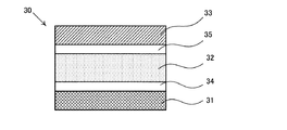
まず、図3を用いて、第3の実施形態に係る光電変換素子の構成について説明する。図3は、本実施形態に係る有機EL素子30(光電変換素子)の構成概略図である。有機EL素子30は、この素子に入力された電気エネルギーを光に変換する発光素子としての機能を有する素子である。有機EL素子30は、透明電極31の表面に設けられた光電変換層(発光層)32と、光電変換層32の透明電極31の反対側面に設けられた対向電極33とを具備している。
[Third Embodiment]
First, the configuration of the photoelectric conversion element according to the third embodiment will be described with reference to FIG. FIG. 3 is a schematic configuration diagram of the organic EL element 30 (photoelectric conversion element) according to the present embodiment. The
ここで透明電極21は実施形態1で示されたものと同様である。
Here, the
光電変換層32は、透明電極31から注入された電荷と対向電極33から注入された電荷を再結合させ電気エネルギーを光に変換させる有機薄膜層である。光電変換層32は通常p型の半導体層とn型の半導体層からなっている。光電変換層32と対向電極33の間には電荷注入を促進もしくはブロックするためバッファ層35が設けられ、光電変換層32と透明電極31の間にもバッファ層34が設けられていてもよい。
The photoelectric conversion layer 32 is an organic thin film layer that recombines the charges injected from the
対向電極33は、通常は金属電極であるが透明電極を用いてもよい。対向電極33と光電変換層(発光層)32の間には電荷注入を促進もしくはブロックするためにバッファ層35が挿入されていてもよい。
The counter electrode 33 is usually a metal electrode, but a transparent electrode may be used. A
遮蔽層として自己ドープ型導電性ポリマー層を用いる場合には、透明電極31が陽極となる構成が好ましい。
When the self-doping type conductive polymer layer is used as the shielding layer, the
遮蔽層としてN−グラフェン膜を用いる場合には、透明電極31は陽極および陰極にもすることができる。ただし、陽極となる透明電極に、遮蔽層としてN−グラフェン膜を用いる場合には、N−グラフェン膜と光電変換層32との間にイオン化ポテンシャルを大きくするバッファ層を設置することが好ましい。このようなバッファ層としては例えばバナジウム酸化物、PEDOT/PSS、p型ポリマー、五酸化バナジウム、Spiro−OMeTAD、酸化ニッケル、三酸化タングステン、三酸化モリブデン等からなる層を用いることができる。
When an N-graphene film is used as the shielding layer, the
一方、陰極となる透明電極に、遮蔽層としてN−グラフェン膜を用いる場合には、N−グラフェン層と光電変換層22との間に仕事関数を小さくするバッファ層24を設置することが好ましい。このようなバッファ層としては亜鉛酸化物、チタン酸化物、フッ化リチウム、炭酸セシウム、ポリエチレンイミン類、等がある。
On the other hand, when an N-graphene film is used as the shielding layer for the transparent electrode serving as the cathode, it is preferable to dispose the
なお、実施形態2と同様に、遮蔽層に代えて、あるいは、遮蔽層と光電変換層との間に、ブルッカイト型酸化チタン層を設けることができる。 Note that, as in Embodiment 2, a brookite-type titanium oxide layer can be provided instead of the shielding layer or between the shielding layer and the photoelectric conversion layer.
対向電極33として、透明電極31と同様の透明電極を用いてもよい。また透明電極として、実施形態2において説明したグラフェン膜を用いてもよい。
A transparent electrode similar to the
実施形態による有機EL素子は、両面を透明電極に挟まれた構造とすることができる。
このような構造を有する有機EL素子は、両面発光が可能であり、長期間安定でフレキシブルである。
The organic EL element according to the embodiment may have a structure in which both surfaces are sandwiched by transparent electrodes.
The organic EL element having such a structure can emit light from both sides, is stable and flexible for a long period of time.
[実施形態4]
第4の実施形態に係る電子デバイスの製造方法を、図4を参照しながら説明すると以下の通りである。
実施形態による電子デバイス40の製造方法は、導電層41、遮蔽層42、光電変換層43、対抗電極44を接合させることにより製造することができる。これらの各層および電極は、それぞれ独立に形成させてから接合しても、各層を順次積層形成させてもよい。
各層の形成方法について説明すると以下の通りである。
[Embodiment 4]
The method of manufacturing the electronic device according to the fourth embodiment will be described below with reference to FIG.
The method for manufacturing the
The method of forming each layer is as follows.
導電層41は基板を有しない単独の膜であってもよいが、基板の表面に形成されていてもよい。一般的には、製造を容易にするために、基板の表面に導電層を形成させることが好ましい。
The
実施形態において、導電層41はアモルファス無機酸化物を含有する層である。アモルファス無機酸化物としては、ITOやFTOが好ましく用いられる。これらのアモルファス無機酸化物の膜は、一般的にはスパッタリング法により形成される。また、印刷法により形成されてもよい。
In the embodiment, the
導電層41は、金属薄膜を有していてもよい。導電層が金属薄膜を有する場合には、無機酸化物を含む膜の上に直接形成させても、無機酸化物を含む膜に金属薄膜を貼り付けてもよい。
The
導電層41に接合する遮蔽層42は、(i)ポリマー膜、(ii)N−グラフェン膜、および(iii)ポリマー膜とN−グラフェン膜との組み合わせのいずれかである。
遮蔽層としてポリマー膜を用いる場合には、前記した自己ドープ型導電性ポリマーを含む水溶液を調製し、その水溶液を塗布乾燥することによって形成させることができる。ポリマー水溶液のpHは、3以上とすることが好ましい。このようなpHとすることで、自己ドープ型導電性ポリマーのブレンステッド酸の共役塩基が陰イオンとして存在することが可能となり、光電変換層に含まれるハロゲンイオン等の陰イオンの電極への拡散を防ぐことができる。この結果、電極の劣化を防いだり、デバイス外部から光電変換層への陰イオン等の拡散を防ぐことが可能となり、電子デバイスの耐久性を向上することができる。
なお、ポリマー水溶液のpHは11以下であることが好ましい。ポリマーとして非自己ドープ型導電性ポリマーを用いた場合には、強酸性であるpH2以下であることが必要となり、実施形態の効果を達成することが困難となる。なお、ポリマー水溶液には、ポリオール化合物もしくは酸化グラフェンを添加することができる。これらの添加物を用いることで、隣接層との接着性を高めることから好ましい。なお、ポリマー膜は、導電層の上に直接形成させても、ほかの基板上に形成させたポリマー膜を、前記した導電層の上に転写などにより設置することもできる。
The
When a polymer film is used as the shielding layer, it can be formed by preparing an aqueous solution containing the above-mentioned self-doping type conductive polymer, and applying and drying the aqueous solution. The pH of the aqueous polymer solution is preferably 3 or more. By setting such a pH, the conjugate base of Bronsted acid of the self-doping type conductive polymer can exist as an anion, and diffusion of anions such as halogen ions contained in the photoelectric conversion layer to the electrode. Can be prevented. As a result, it is possible to prevent the deterioration of the electrodes and prevent the diffusion of anions and the like from the outside of the device to the photoelectric conversion layer, and it is possible to improve the durability of the electronic device.
The pH of the polymer aqueous solution is preferably 11 or less. When a non-self-doping type conductive polymer is used as the polymer, it is necessary that the pH is 2 or less, which is strongly acidic, and it becomes difficult to achieve the effects of the embodiment. A polyol compound or graphene oxide can be added to the polymer aqueous solution. The use of these additives is preferable because it enhances the adhesiveness with the adjacent layer. The polymer film may be directly formed on the conductive layer, or the polymer film formed on another substrate may be placed on the conductive layer by transfer or the like.
遮蔽層としてN−グラフェン膜用いる場合には、N−グラフェン膜を例えば以下の方法によって形成させる。 When the N-graphene film is used as the shielding layer, the N-graphene film is formed by the following method, for example.
まず、下地触媒として銅箔を準備し、その表面をレーザー照射によってアニール処理し、結晶粒を大きくする。次いで、その銅箔の表面に、アンモニア、メタン、水素、およびアルゴン(15:60:65:200ccm)を反応ガスとして、1000℃/5分の条件下、化学気相蒸着法(以下、CVDという)により膜を作製する。得られた膜を、アンモニア、アルゴン気流下1000℃で5分間、さらに処理した後、アルゴン下で冷却することによって、単層のN−グラフェン膜を得ることができる。 First, a copper foil is prepared as a base catalyst, and its surface is annealed by laser irradiation to enlarge crystal grains. Then, on the surface of the copper foil, ammonia, methane, hydrogen, and argon (15: 60: 65: 200 ccm) were used as reaction gases, under the condition of 1000 ° C./5 minutes, a chemical vapor deposition method (hereinafter referred to as CVD). To produce a film. A single-layer N-graphene film can be obtained by further treating the obtained film under an atmosphere of ammonia and argon at 1000 ° C. for 5 minutes and then cooling under argon.
単層N−グラフェン膜の表面に熱転写フィルムを圧着した後、アンモニアアルカリ性の塩化第二銅エッチャントに漬けて、銅箔を溶解し、単層グラフェンを熱転写フィルム上に転写する。同様の操作を繰り返すことにより、熱転写フィルム上に単層グラフェンが2〜4層積層された多層N−グラフェン膜を得ることができる。 After the thermal transfer film is pressure-bonded to the surface of the single-layer N-graphene film, it is immersed in an ammoniacal cupric chloride etchant to dissolve the copper foil, and the single-layer graphene is transferred onto the thermal transfer film. By repeating the same operation, a multilayer N-graphene film in which 2 to 4 single-layer graphene layers are laminated on the thermal transfer film can be obtained.
上記したN−グラフェン膜の製造法において、CVD法の原料としてアンモニアガスの代わりにピリジンやメチルアミン、エチレンジアミン、尿素などの低分子窒素化合物やメタンの代わりにエチレンやアセチレン、メタノール、エタノール等を用いてもよい。 In the above-mentioned method for producing the N-graphene film, low molecular nitrogen compounds such as pyridine, methylamine, ethylenediamine, and urea instead of ammonia gas and ethylene, acetylene, methanol, ethanol, etc. are used as raw materials for the CVD method instead of methane. May be.
N−グラフェン膜はその他の方法でも形成することができる。例えば、酸化グラフェンの水分散液を石英ガラス上や金属上(例えばCu)にスピンコートして薄膜状にした後、アンモニア、水素、アルゴンの混合雰囲気下で熱処理して窒素置換して製造することができる。または酸化グラフェン薄膜をヒドラジンで加熱処理して乾燥させて製造することができる。または、無置換グラフェン薄膜を窒素プラズマ中で処理して製造することもできる。
さらには、ポリアクリロニトリル、ポリイミドなどの含窒素ポリマー化合物を石英ガラス上や金属上に塗布して薄膜を形成し、それを真空中やアルゴン下で加熱することによりグラファイト化することによっても製造できる。また窒素置換グラフェンの分散液を作製し、その分散液を石英ガラスなどに塗布する方法や、グラフェン分散液をフィルターでろ過してフィルター上にN−グラフェンを堆積させることにより膜を作製し、フィルターから剥離して膜を作製できる。
The N-graphene film can also be formed by other methods. For example, it is manufactured by spin-coating an aqueous dispersion of graphene oxide on quartz glass or metal (for example, Cu) to form a thin film, and then heat-treating in a mixed atmosphere of ammonia, hydrogen, and argon to replace nitrogen. You can Alternatively, the graphene oxide thin film can be manufactured by heat treatment with hydrazine and drying. Alternatively, the unsubstituted graphene thin film can be manufactured by treating it in nitrogen plasma.
Further, it can be also produced by coating a nitrogen-containing polymer compound such as polyacrylonitrile or polyimide on quartz glass or metal to form a thin film, and heating it in vacuum or under argon to graphitize it. In addition, a method of preparing a dispersion liquid of nitrogen-substituted graphene and applying the dispersion liquid to quartz glass, or a method of filtering the graphene dispersion liquid with a filter and depositing N-graphene on the filter to form a film, The film can be produced by peeling from
実施形態による透明電極において、このように形成されたN−グラフェン層は、導電層の上に直接、または前記したポリマー膜を介して導電層の上に間接的に、設置されている。この設置は後述するように、熱転写フィルムから転写されることによって行われるのが一般的である。このとき、あらかじめ導電層に集電用の金属配線を形成させておいてもよい。 In the transparent electrode according to the embodiment, the N-graphene layer thus formed is provided directly on the conductive layer or indirectly on the conductive layer via the polymer film described above. This installation is generally performed by transferring from a thermal transfer film, as described later. At this time, a metal wiring for collecting current may be formed on the conductive layer in advance.
遮蔽膜として、ポリマー膜とN−グラフェン膜との組み合わせを用いる場合には、導電層の直上にN−グラフェン膜を設置し、その上にポリマー膜を形成または設置することが好ましい。 When the combination of the polymer film and the N-graphene film is used as the shielding film, it is preferable that the N-graphene film is provided directly on the conductive layer and the polymer film is formed or provided thereon.
光電変換層43の形成方法は、用いられる材料に応じて適切に選択され、特に限定されない。たとえばペロブスカイト太陽電池ではペロブスカイト化合物前駆体溶液を塗布し、乾燥することにより光電変換層を形成することができる。また、半導体結晶からなる半導体膜を張り付けることにより光電変換層とすることもできる。
The method for forming the
対抗電極44は、その構成に応じて任意の方法で製造することができる。金属薄膜を光電変換層に接合することや、光電変換層の表面にスパッタ法などにより金属層を積層することもできる。また、実施形態による透明電極を接合したり、単層または多層グラフェン膜を電極として接合することもできる。
The
これら、導電層41、遮蔽層42、光電変換層43、および対抗電極44を接合することで電子デバイス40を形成させる。これらの接合の順序は特に限定されず、任意の順序で、または同時に行うことができる。
The
必要に応じて、導電層または対抗電極に基板を接合したり、遮蔽層42と光電変換層43との間、および/または光電変換層43と対抗電極44との間にバッファ層を挿入して接合することもできる。
If necessary, a substrate may be bonded to the conductive layer or the counter electrode, or a buffer layer may be inserted between the shielding
さらには、バッファ層と光電変換層の間にブルッカイト型酸化チタン層を設けたり、バッファ層に代えてブルッカイト型酸化チタン層を設けたりしてから接合することもできる。このブルッカイト型酸化チタン層は、グラフェン膜を含む遮蔽層と組み合わせることが特に好ましい。ブルッカイト型酸化チタン層は、ブルッカイト型酸化チタンのナノ粒子を極性溶媒中に分散させた分散液を、遮蔽層、バッファ層、または光電変換層の表面に塗布し、乾燥させることで形成させることができる。分散液の濃度は、目的とする層の厚さや電子デバイスの性能などに応じて調整される。ナノ粒子の分散安定性を維持するために、分散液のpHは1〜3であることが好ましい。塗布方法は、スピンコート、バーコート、スプレーコートなど、任意の方法を採用することができる。塗布後、高温、例えば100〜150℃に加熱することで乾燥が好ましい。なお、分散液の濃度が低い場合、塗布後に直ちに加熱を行うと、ナノ粒子の凝集が起こる場合がある。このため、加熱に先立って、溶媒の大部分を一般に35℃以下、例えば室温において除去した後、加熱して高温に付することが好ましい。 Further, a brookite type titanium oxide layer may be provided between the buffer layer and the photoelectric conversion layer, or a brookite type titanium oxide layer may be provided instead of the buffer layer before joining. This brookite-type titanium oxide layer is particularly preferably combined with a shielding layer containing a graphene film. The brookite-type titanium oxide layer can be formed by applying a dispersion liquid in which nanoparticles of brookite-type titanium oxide are dispersed in a polar solvent to the surface of the shielding layer, the buffer layer, or the photoelectric conversion layer and drying. it can. The concentration of the dispersion liquid is adjusted according to the thickness of the target layer and the performance of the electronic device. The pH of the dispersion is preferably 1 to 3 in order to maintain the dispersion stability of the nanoparticles. As a coating method, any method such as spin coating, bar coating, and spray coating can be adopted. After application, it is preferable to dry by heating at a high temperature, for example, 100 to 150 ° C. When the concentration of the dispersion liquid is low, the nanoparticles may aggregate if heated immediately after coating. For this reason, it is preferable to remove most of the solvent generally at 35 ° C. or lower, for example, at room temperature prior to heating, and then heat to high temperature.
接合は塗布等のウエットプロセス、貼り合わせや転写等のドライプロセス、スパッタや蒸着等の真空プロセス等で作製することができる。この中で貼り合わせや転写は溶媒等の制約がなく、また低温でできるため素子ダメージが少ないために好ましい。貼り合わせ面としては真空貼り合わせ等を用いればすべて面で接合が可能である。素子耐久性の面で接着性があるバッファ層面が好ましく、自己ドープ型導電性ポリマー面が特に好ましい。なお、ここで「接合」とは、いずれかの層の上に直接別の層を形成させることも包含するものとする。 The bonding can be made by a wet process such as coating, a dry process such as bonding and transfer, a vacuum process such as sputtering and vapor deposition. Of these, bonding and transfer are preferable because there is no restriction on the solvent and the like, and the element damage is small because they can be performed at low temperatures. If vacuum bonding or the like is used as the bonding surface, all surfaces can be bonded. In terms of device durability, a buffer layer surface having adhesiveness is preferable, and a self-doping type conductive polymer surface is particularly preferable. Note that, here, “bonding” also includes forming another layer directly on any layer.
(実施例1)
図1に示す構造の透明電極10を作成した。この電極は、a−ITO/銀合金/a−ITOの積層構造(厚さ100nm)を有する導電層が厚さ150μmのPETフィルム上に形成され、その上にブレンステッド酸アニオンと局在化されたカチオンを側鎖に含有する自己ドープ型導電性ポリマー膜である遮蔽層が積層されている。
(Example 1)
A
自己ドープ型導電性ポリマーとして下記式(Ia−x)で示されるスルホン酸基を有するポリチオフェンの10%水溶液に、テトラメチルアンモニウムヒドロキシド水溶液を添加してpH6に調整する。この水溶液をa−ITO/銀合金/a−ITOを有する導電層にバーコーターを用いて塗布した後90℃で1時間乾燥して透明電極を作製する。
この透明電極は15%塩水中での3日間浸漬では電極の導電性や形状に変化は見られない。 This transparent electrode shows no change in conductivity or shape of the electrode when immersed in 15% salt water for 3 days.
(実施例2)
図1に示す構造の透明電極10を作成した。この電極は、a−ITO/銀合金/a−ITOの積層構造(厚さ100nm)を有する導電層が厚さ150μmのPETフィルム上に形成され、その上に平面状の、炭素原子の一部が窒素原子に置換された、平均4層のN−グラフェン膜が積層された遮蔽層が形成されている。
(Example 2)
A
遮蔽層は以下の通り作成する。まず、Cu箔の表面をレーザー照射によって加熱処理し、アニールにより結晶粒を大きくする。このCu箔を下地触媒層とし、アンモニア、メタン、水素、アルゴン(15:60:65:200ccm)を混合反応ガスとして1000℃、5分間の条件下、CVD法により平面状の単層N−グラフェン膜を製造する。この時、ほとんどは単層のグラフェン膜が形成されるが、条件により一部に2層以上のN−グラフェン膜も生成する。さらにアンモニア、アルゴン混合気流下1000℃で5分処理した後、アルゴン気流下で冷却する。熱転写フィルム(150μm厚)と単層N−グラフェンを圧着した後、Cuを溶解するため、アンモニアアルカリ性の塩化第二銅エッチャントに漬けて、単層N−グラフェン膜を熱転写フィルム上に転写する。同様の操作を繰り返すことに単層グラフェン膜を熱転写フィルム上に4層積層して多層N−グラフェン膜を得る。
熱転写フィルムをa−ITO/銀合金/a−ITO/PETフィルムの上にラミネートした後、加熱してN−グラフェン膜をa−ITO/銀合金/a−ITO/PETフィルム上に転写して透明電極を作製する。
The shielding layer is created as follows. First, the surface of the Cu foil is heat-treated by laser irradiation, and crystal grains are enlarged by annealing. This Cu foil is used as a base catalyst layer, and ammonia, methane, hydrogen, and argon (15: 60: 65: 200 ccm) are used as a mixed reaction gas at 1000 ° C. for 5 minutes, and the planar single-layer N-graphene is formed by the CVD method. Produce a membrane. At this time, a single-layer graphene film is formed in most cases, but two or more layers of N-graphene film are also partially formed depending on the conditions. Further, after treatment at 1000 ° C. for 5 minutes in a mixed air stream of ammonia and argon, it is cooled in an argon air stream. After the thermal transfer film (150 μm thick) and the single-layer N-graphene are pressure-bonded, in order to dissolve Cu, the single-layer N-graphene film is transferred onto the thermal transfer film by dipping in an ammonia alkaline cupric chloride etchant. By repeating the same operation, four layers of the single-layer graphene film are laminated on the thermal transfer film to obtain a multilayer N-graphene film.
After the thermal transfer film is laminated on the a-ITO / silver alloy / a-ITO / PET film, it is heated and the N-graphene film is transferred onto the a-ITO / silver alloy / a-ITO / PET film to be transparent. Make the electrodes.
XPSで測定された窒素の含有量は、この条件では1〜2atm%である。XPSから測定したカーボン材料の炭素原子と酸素原子の比率は100〜200である。
この透明電極は15%塩水中での3日間浸漬では導電性や形状に変化は見られない。
The nitrogen content measured by XPS is 1-2 atm% under these conditions. The ratio of carbon atoms to oxygen atoms of the carbon material measured by XPS is 100 to 200.
This transparent electrode shows no change in conductivity or shape when immersed in 15% salt water for 3 days.
(実施例3)
図1に示す構造の透明電極10を作成した。この電極は、a−ITO/銀合金/a−ITOの積層構造(厚さ100nm)を有する導電層が厚さ150μmのPETフィルム上に形成され、その上に平面状の、炭素原子の一部が窒素原子に置換された、平均2層のN−グラフェン膜が積層された遮蔽層が形成されている。
(Example 3)
A
遮蔽層は以下の通り作成した。まず、a−ITO/銀合金/a−ITOの積層構造を有する導電層を準備する。この導電層のITO表面をUVオゾン処理して親水性にしておく。次いで、酸化グラフェンの水溶液をUVオゾン処理した導電層上にバーコーターで塗布する。グラフェン膜の膜厚は酸化グラフェンの濃度とバーコーターのバーと導電層との距離で調整することができる。塗布後、90℃で20分乾燥し、さらに110℃の水和ヒドラジン蒸気で1時間処理して、酸化グラフェン膜の炭素の一部が窒素原子に置換された2層グラフェン膜を具備した透明電極を作製する。 The shielding layer was prepared as follows. First, a conductive layer having a laminated structure of a-ITO / silver alloy / a-ITO is prepared. The ITO surface of this conductive layer is treated with UV ozone to make it hydrophilic. Next, an aqueous solution of graphene oxide is applied on the UV ozone-treated conductive layer with a bar coater. The thickness of the graphene film can be adjusted by the concentration of graphene oxide and the distance between the bar of the bar coater and the conductive layer. After coating, it was dried at 90 ° C. for 20 minutes, and further treated with hydrated hydrazine vapor at 110 ° C. for 1 hour to form a transparent electrode having a two-layer graphene film in which part of carbon in the graphene oxide film was replaced with nitrogen atoms. To make.
この透明電極は15%塩水中での3日間浸漬では導電性や形状に変化は見られない。 This transparent electrode shows no change in conductivity or shape when immersed in 15% salt water for 3 days.
(実施例4)
図1に示す構造の透明電極10を作成する。この電極は、a−ITO/銀合金/a−ITOの積層構造(厚さ100nm)を有する導電層が厚さ150μmのPETフィルム上に形成され、その上に平面状の、炭素原子の一部が窒素原子に置換され、平均2層のN−グラフェン膜と、ブレンステッド酸アニオンと局在化されたカチオンを側鎖に含有する自己ドープ型導電性ポリマー膜が積層された遮蔽層が形成されている。
(Example 4)
A
この透明電極は、実施例3で得られる透明電極上に、実施例1と同様の方法でポリマー積層することにより作製する。
この透明電極は20%塩水中での3日間浸漬では導電性や形状に変化は見られない。
This transparent electrode is produced by laminating a polymer on the transparent electrode obtained in Example 3 in the same manner as in Example 1.
This transparent electrode shows no change in conductivity or shape when immersed in 20% salt water for 3 days.
(実施例5)
図1に示す構造の透明電極10を作成する。この電極は、a−ITO(厚さ400nm)を有する導電層が厚さ150μmのPETフィルム上に形成され、その上に平面状の、炭素原子の一部が窒素原子に置換され、平均2層のN−グラフェン膜が積層された遮蔽層が形成されている。
(Example 5)
A
この透明電極は、導電層を変更し、実施例3と同様の方法で作成する。 This transparent electrode is prepared in the same manner as in Example 3 except that the conductive layer is changed.
この透明電極はpH1.5の塩酸中での2日間浸漬では導電性や形状に変化は見られない。また浸漬後の塩酸中には、溶解したインジウムやスズは検出されない。 This transparent electrode shows no change in conductivity or shape when immersed in hydrochloric acid having a pH of 1.5 for 2 days. Further, dissolved indium and tin are not detected in the hydrochloric acid after the immersion.
(実施例6)
図1に示す構造の透明電極10を作成する。この電極は、a−ITO(厚さ400nm)を有する導電層が厚さ150μmのPETフィルム上に形成され、その上に平面状の、炭素原子の一部が窒素原子に置換され、平均2層のN−グラフェン膜と、ブレンステッド酸アニオンと局在化されたカチオンを側鎖に含有する自己ドープ型導電性ポリマー膜が積層された遮蔽層が形成されている。
(Example 6)
A
この透明電極は、導電層を変更し、実施例4と同様の方法で作成する。 This transparent electrode is prepared in the same manner as in Example 4, except that the conductive layer is changed.
この透明電極にpH1.5のPEDOT・PSSの水溶液を塗布し110℃で15分乾燥する。この透明電極は大気中での1週間放置では導電性や形状に変化は見られない。また放置後の透明電極の断面を走査型電子顕微鏡での観察ではPEDOT・PSS層中に溶解したインジウムやスズは検出されない。 An aqueous solution of PEDOT / PSS having a pH of 1.5 is applied to this transparent electrode and dried at 110 ° C. for 15 minutes. This transparent electrode shows no change in conductivity or shape when left in the atmosphere for one week. Further, when the cross section of the transparent electrode after standing is observed with a scanning electron microscope, indium and tin dissolved in the PEDOT / PSS layer are not detected.
(実施例7)
図1に示す構造の透明電極10を作成する。この電極は、a−ZnO(厚さ400nm)を有する導電層が厚さ150μmのPETフィルム上に形成され、その上に平面状の、炭素原子の一部が窒素原子に置換された、平均2層のN−グラフェン膜と、ブレンステッド酸アニオンと局在化されたカチオンを側鎖に含有する自己ドープ型導電性ポリマー膜が積層された遮蔽層が形成されている。
(Example 7)
A
この透明電極は、導電層を変更し、実施例4と同様の方法で作成する。 This transparent electrode is prepared in the same manner as in Example 4, except that the conductive layer is changed.
この透明電極にpH1.5のPEDOT・PSSの水溶液を塗布し110℃で15分乾燥する。この透明電極は大気中での1週間放置では導電性や形状に変化は見られない。また放置後の透明電極の断面を走査型電子顕微鏡で観察ではPEDOT・PSS層中に溶解したインジウムやスズは検出されない。 An aqueous solution of PEDOT / PSS having a pH of 1.5 is applied to this transparent electrode and dried at 110 ° C. for 15 minutes. This transparent electrode shows no change in conductivity or shape when left in the atmosphere for one week. In addition, when the cross section of the transparent electrode after standing is observed with a scanning electron microscope, indium and tin dissolved in the PEDOT / PSS layer are not detected.
(比較例1)
厚さ150μmのPETフィルム上に、ITO/銀合金/ITOの積層構造(厚さ100nm)が形成された透明導電フィルムを、25%塩水中に3日間浸漬したところ、導電性が低下し、表面に白点が観察される。この白点は、銀合金と塩化物イオンの反応により形成されるものである。
(Comparative Example 1)
When a transparent conductive film in which a laminated structure of ITO / silver alloy / ITO (thickness 100 nm) was formed on a PET film having a thickness of 150 μm was immersed in 25% salt water for 3 days, the conductivity was lowered and the surface was reduced. White spots are observed. The white spots are formed by the reaction of silver alloy and chloride ions.
(比較例2)
厚さ150μmのPETフィルム上にa−ITO(厚さ400nm)からなる導電層が形成された透明導電フィルムを、pH1.5の塩酸中2日間浸漬すると、導電性が低下する。また、浸漬後の塩酸中に溶解したインジウムやスズが検出される。
(Comparative example 2)
When a transparent conductive film in which a conductive layer made of a-ITO (thickness 400 nm) is formed on a PET film having a thickness of 150 μm is immersed in hydrochloric acid having a pH of 1.5 for 2 days, the conductivity decreases. In addition, indium and tin dissolved in hydrochloric acid after immersion are detected.
(実施例8)
図2に示す太陽電池セルを作成する。この太陽電池セルは、
(a)厚さ150μmのPETフィルム、
(b)a−ITO/銀合金/a−ITOの積層構造(厚さ100nm)を有する導電層、(c)平面状の、2層N−グラフェン膜、
(d)ブレンステッド酸アニオンと局在化されたカチオンを側鎖に含有する自己ドープ型導電性ポリマー膜、
(e)ペロブスカイト型有機無機ハイブリッド型光電変換層、
(f)バッファ層、
(g)平面状の、4層N−グラフェン膜
(h)a−ITO/銀合金/a−ITOの積層構造(厚さ100nm)を有する導電層、および
(i)厚さ150μmのPETフィルム
がこの順序で積層される。ここで、(c)と(d)とが遮蔽層を構成し、(b)、(c)および(d)が実施形態による透明電極を構成し、(g)と(h)とが対向電極を構成する。なお、この対向電極も実施形態による透明電極であり、(g)も遮蔽層である。
(Example 8)
The solar battery cell shown in FIG. 2 is created. This solar cell is
(A) PET film having a thickness of 150 μm,
(B) a conductive layer having a laminated structure of a-ITO / silver alloy / a-ITO (thickness 100 nm), (c) a planar two-layer N-graphene film,
(D) a self-doped conductive polymer film containing a Bronsted acid anion and a localized cation in a side chain,
(E) Perovskite type organic-inorganic hybrid type photoelectric conversion layer,
(F) a buffer layer,
(G) a planar 4-layer N-graphene film (h) a conductive layer having a laminated structure of a-ITO / silver alloy / a-ITO (thickness 100 nm), and (i) a PET film having a thickness of 150 μm. The layers are stacked in this order. Here, (c) and (d) form a shielding layer, (b), (c) and (d) form a transparent electrode according to the embodiment, and (g) and (h) form a counter electrode. Make up. The counter electrode is also a transparent electrode according to the embodiment, and (g) is also a shielding layer.
この太陽電池を以下の方法で作成する。 This solar cell is prepared by the following method.
PETフィルム(a)の上に導電層(b)を形成させる。次いで導電層のITO表面をUVオゾン処理して親水性にする。ついで、そのITO表面上に酸化グラフェン水溶液をバーコーターで塗布する。90℃で20分乾燥した後、110℃で水和ヒドラジン蒸気で1時間処理して酸化グラフェンが一部窒素原子に置換された2層N−グラフェン膜(c)に変化させる。次に、式(Ia−x)で示されるポリチオフェンの10%水溶液に、メチルアミン水溶液を添加してpH6に調整し、ポリマーに対して5%のソルビト−ル(低分子ポリオール化合物)を混合して、自己ドープ型導電性ポリマー水溶液を調製する。この水溶液をN−グラフェン膜(c)上にバーコーターを用いて塗布した後90℃で1時間乾燥して、ポリマー膜(d)を形成させ、透明電極を作製する。 A conductive layer (b) is formed on the PET film (a). Next, the ITO surface of the conductive layer is treated with UV ozone to make it hydrophilic. Then, an aqueous graphene oxide solution is applied onto the ITO surface with a bar coater. After drying at 90 ° C. for 20 minutes, it is treated with hydrated hydrazine vapor at 110 ° C. for 1 hour to change into a bilayer N-graphene film (c) in which graphene oxide is partially replaced with nitrogen atoms. Next, an aqueous solution of methylamine was added to a 10% aqueous solution of polythiophene represented by the formula (Ia-x) to adjust the pH to 6, and 5% of sorbitol (low molecular weight polyol compound) was mixed with the polymer. Thus, a self-doping type conductive polymer aqueous solution is prepared. This aqueous solution is applied onto the N-graphene film (c) by using a bar coater, and then dried at 90 ° C. for 1 hour to form a polymer film (d) to produce a transparent electrode.
対向電極および光電変換層は以下の通り作成する。PETフィルム(i)の表面に導電層(h)を形成させる。この導電層の表面に、実施例2と同様の方法で4層N−グラフェン膜(g)を形成させる。このN−グラフェン膜上にC60−PCBMのトルエン溶液をバーコーターで塗布してバッファ層(f)を形成させる。その上にPbI2のジメチルホルムアミド溶液(20wt%)を、バーコーターで塗布し、次いで、CH3NH3Iのイソプロピルアルコール溶液(2wt%)を、バーコーターで塗布し、90℃で30分乾燥することにより光電変換層(e)を形成させる。 The counter electrode and the photoelectric conversion layer are formed as follows. A conductive layer (h) is formed on the surface of the PET film (i). A four-layer N-graphene film (g) is formed on the surface of this conductive layer by the same method as in Example 2. A buffer solution (f) is formed by coating a toluene solution of C60-PCBM on the N-graphene film with a bar coater. A dimethylformamide solution of PbI 2 (20 wt%) was applied thereon by a bar coater, and then an isopropyl alcohol solution of CH 3 NH 3 I (2 wt%) was applied by a bar coater and dried at 90 ° C. for 30 minutes. By doing so, the photoelectric conversion layer (e) is formed.
透明電極と、対向電極の上に形成した光電変換層とを、80℃、乾燥大気中で貼り合わせ、周りを封止することにより両面が透明な太陽電池セルを作製する。
得られる太陽電池セルは1SUNの太陽光に対して14%以上のエネルギー変換効率を示し、一か月放置しても効率の劣化は5%未満である。
A transparent electrode and a photoelectric conversion layer formed on the counter electrode are attached to each other in a dry atmosphere at 80 ° C., and the periphery is sealed to produce a solar cell having transparent both sides.
The obtained solar battery cell exhibits an energy conversion efficiency of 14% or more with respect to 1 SUN of sunlight, and the efficiency deterioration is less than 5% even if left for one month.
(実施例9)
図2に示す太陽電池セルを作成した。この太陽電池セルは、ポリマー水溶液のpH調整にメチルアミンに代えて1,4−ジアミノブタンを用い、光電変換層の形成にCH3NH3Iに代えて(CH3)2NH2Brを用いた他は、実施例8と同様の方法で作成する。
(Example 9)
The solar battery cell shown in FIG. 2 was created. In this solar cell, 1,4-diaminobutane was used in place of methylamine for pH adjustment of the polymer aqueous solution, and (CH 3 ) 2 NH 2 Br was used in place of CH 3 NH 3 I for formation of the photoelectric conversion layer. Except for the above, the method is similar to that of the eighth embodiment.
得られる太陽電池セルは1SUNの太陽光に対して14%以上のエネルギー変換効率を示し、一か月放置しても効率の劣化は3%未満である。 The obtained solar cell shows an energy conversion efficiency of 14% or more with respect to 1 SUN of sunlight, and the efficiency deterioration is less than 3% even if left for one month.
(実施例10)
図2に示す太陽電池セルを作成した。この太陽電池セルは、
(a)厚さ150μmのPETフィルム、
(b)a−ITO/銀合金/a−ITOの積層構造(厚さ100nm)を有する導電層、(c)平面状の、2層N−グラフェン膜、
(d)ブレンステッド酸アニオンと局在化されたカチオンを側鎖に含有する自己ドープ型導電性ポリマー膜、
(e)バッファ層、
(f)ペロブスカイト型有機無機ハイブリッド型光電変換層、
(g)バッファ層、
(h)銀電極層
がこの順序で積層される。ここで、(c)と(d)とが遮蔽層を構成し、(b)、(c)および(d)が実施形態による透明電極を構成する。
(Example 10)
The solar battery cell shown in FIG. 2 was created. This solar cell is
(A) PET film having a thickness of 150 μm,
(B) a conductive layer having a laminated structure of a-ITO / silver alloy / a-ITO (thickness 100 nm), (c) a planar two-layer N-graphene film,
(D) a self-doped conductive polymer film containing a Bronsted acid anion and a localized cation in a side chain,
(E) a buffer layer,
(F) Perovskite type organic-inorganic hybrid type photoelectric conversion layer,
(G) a buffer layer,
(H) The silver electrode layers are laminated in this order. Here, (c) and (d) form a shielding layer, and (b), (c) and (d) form a transparent electrode according to the embodiment.
この太陽電池を以下の方法で作成する。
PETフィルム(a)の上に導電層(b)を形成させる。次いで導電層のITO表面をUVオゾン処理して親水性にする。ついで、そのITO表面上に酸化グラフェン水溶液をバーコーターで塗布する。90℃で20分乾燥した後、110℃で水和ヒドラジン蒸気で1時間処理して酸化グラフェンが一部窒素原子に置換された2層N−グラフェン膜(c)に変化させる。次に、式(Ia−1)で示されるポリチオフェンの10%水溶液に、メチルアミン水溶液を添加してpH6に調整し、ポリマーに対して5%のソルビト−ル(低分子ポリオール化合物)を混合して、自己ドープ型導電性ポリマー水溶液を調製する。この水溶液をN−グラフェン膜(c)上にバーコーターを用いて塗布した後90℃で1時間乾燥して、ポリマー膜(d)を形成させ、透明電極を作製する。
This solar cell is prepared by the following method.
A conductive layer (b) is formed on the PET film (a). Next, the ITO surface of the conductive layer is treated with UV ozone to make it hydrophilic. Then, an aqueous graphene oxide solution is applied onto the ITO surface with a bar coater. After drying at 90 ° C. for 20 minutes, it is treated with hydrated hydrazine vapor at 110 ° C. for 1 hour to change into a bilayer N-graphene film (c) in which graphene oxide is partially replaced with nitrogen atoms. Next, an aqueous solution of methylamine was added to a 10% aqueous solution of polythiophene represented by the formula (Ia-1) to adjust the pH to 6, and 5% of sorbitol (low molecular weight polyol compound) was mixed with the polymer. Thus, a self-doping type conductive polymer aqueous solution is prepared. This aqueous solution is applied onto the N-graphene film (c) by using a bar coater, and then dried at 90 ° C. for 1 hour to form a polymer film (d) to produce a transparent electrode.
透明電極の上に、PEDOT・PSSの水溶液をバーコーターで塗布し、100℃で30分乾燥してPEDOT・PSSを含むバッファ層(e)(50nm厚)を形成させる。 An aqueous solution of PEDOT.PSS is applied onto the transparent electrode with a bar coater and dried at 100.degree. C. for 30 minutes to form a buffer layer (e) (50 nm thick) containing PEDOT.PSS.
バッファ層(e)上にPbI2のジメチルホルムアミド溶液(20wt%)を、バーコーターで塗布し、次いで、CH3NH3Brのイソプロピルアルコール溶液(2wt%)を、バーコーターで塗布してから、90℃で30分乾燥することによって光電変換層(f)を形成させる。 A dimethylformamide solution of PbI 2 (20 wt%) was applied on the buffer layer (e) by a bar coater, and then an isopropyl alcohol solution of CH 3 NH 3 Br (2 wt%) was applied by a bar coater, The photoelectric conversion layer (f) is formed by drying at 90 ° C. for 30 minutes.
光電変換層(f)の上にC60−PCBMのトルエン溶液をバーコーターで塗布して乾燥することにより、バッファ層(g)を形成させる。 A buffer layer (g) is formed by applying a toluene solution of C60-PCBM on the photoelectric conversion layer (f) with a bar coater and drying.
対向電極(h)としてバッファ層(g)の上に銀膜をスパッタで作製し、周りを封止することにより太陽電池セルを作製する。 A silver film is formed as a counter electrode (h) on the buffer layer (g) by sputtering, and the periphery is sealed to manufacture a solar battery cell.
得られる太陽電池セルは1SUNの太陽光に対して12%以上のエネルギー変換効率を示し、一か月放置しても効率の劣化は7%未満である。 The obtained solar cell has an energy conversion efficiency of 12% or more with respect to 1 SUN of sunlight, and the efficiency deterioration is less than 7% even if left for one month.
(実施例11)
図2に示す太陽電池セルを作成する。この太陽電池セルは、
(a)ステンレス箔からなる金属薄膜電極(対向電極)、
(b)平面状の、2層N−グラフェン膜
(c)バッファ層、
(d)ペロブスカイト型有機無機ハイブリッド型光電変換層、
(e)バッファ層、
(f)平面状の、2層N−グラフェン膜、
(g)a−ITO(厚さ400nm)からなる導電層
(h)銅からなる補助電極層
がこの順序で積層される。ここで、(f)が遮蔽層を構成し、(f)および(g)が実施形態による透明電極を構成する。
(Example 11)
The solar battery cell shown in FIG. 2 is created. This solar cell is
(A) Metal thin film electrode (counter electrode) made of stainless steel foil,
(B) a planar two-layer N-graphene film (c) buffer layer,
(D) Perovskite type organic-inorganic hybrid type photoelectric conversion layer,
(E) a buffer layer,
(F) a planar two-layer N-graphene film,
(G) A conductive layer made of a-ITO (thickness 400 nm) (h) An auxiliary electrode layer made of copper is laminated in this order. Here, (f) forms the shielding layer, and (f) and (g) form the transparent electrode according to the embodiment.
ステンレス箔(a)の表面を、希塩酸で処理して表面酸化膜を除去してから酸化グラフェンの水溶液をバーコーターで塗布して酸化グラフェン膜を形成させる。次いで、90℃で20分乾燥した後、110℃で水和ヒドラジン蒸気で1時間処理して酸化グラフェンの炭素原子の一部が窒素原子に置換された2層N−グラフェン膜(b)に変化させる。 The surface of the stainless steel foil (a) is treated with dilute hydrochloric acid to remove the surface oxide film, and then an aqueous graphene oxide solution is applied by a bar coater to form a graphene oxide film. Then, after drying at 90 ° C. for 20 minutes, it was treated with hydrated hydrazine vapor at 110 ° C. for 1 hour to change into a two-layer N-graphene film (b) in which some of the carbon atoms of graphene oxide were replaced with nitrogen atoms. Let
N−グラフェン膜(b)の上に、PEDOT・PSSの水溶液をバーコーターで塗布し、100℃で30分乾燥してPEDOT・PSSを含むバッファ層(c)(50nm厚)を形成させる。 An aqueous solution of PEDOT.PSS is applied on the N-graphene film (b) with a bar coater and dried at 100 ° C. for 30 minutes to form a buffer layer (c) (50 nm thick) containing PEDOT.PSS.
バッファ層(c)上にPbI2のジメチルホルムアミド溶液(20wt%)を、バーコーターで塗布し、次いで、CH3NH3Brのイソプロピルアルコール溶液(2wt%)を、バーコーターで塗布してから、90℃で30分乾燥することによって光電変換層(d)を形成させる。 A dimethylformamide solution of PbI 2 (20 wt%) was applied on the buffer layer (c) by a bar coater, and then an isopropyl alcohol solution of CH 3 NH 3 Br (2 wt%) was applied by a bar coater, The photoelectric conversion layer (d) is formed by drying at 90 ° C. for 30 minutes.
光電変換層(d)の上にバッファ層としてC60−PCBMのトルエン溶液をバーコーターで塗布して乾燥させ、バッファ層(e)を形成させる。 A buffer layer (e) is formed by applying a toluene solution of C60-PCBM as a buffer layer on the photoelectric conversion layer (d) using a bar coater and drying.
バッファ層(e)の上に酸化グラフェン水溶液をバーコーターで塗布する。90℃で20分乾燥した後、110℃で水和ヒドラジン蒸気で1時間処理して酸化グラフェンが一部窒素原子に置換された2層N−グラフェン膜(f)に変化させる。 An aqueous graphene oxide solution is applied onto the buffer layer (e) with a bar coater. After drying at 90 ° C. for 20 minutes, it is treated with hydrated hydrazine vapor at 110 ° C. for 1 hour to change into a bilayer N-graphene film (f) in which graphene oxide is partially replaced with nitrogen atoms.
N−グラフェン膜(f)の表面にa−ITOをスパッタで製膜し、さらに補助電極として銅をスパッタして補助配線を作製して透明電極を形成させる。さらに周りを封止することにより太陽電池セルを作製する。 On the surface of the N-graphene film (f), a-ITO is formed by sputtering, and further copper is sputtered as an auxiliary electrode to form an auxiliary wiring to form a transparent electrode. Further, the periphery is sealed to produce a solar cell.
得られる太陽電池セルは1SUNの太陽光に対して12%以上のエネルギー変換効率を示し、一か月放置しても効率の劣化は3%未満である。 The obtained solar battery cell exhibits an energy conversion efficiency of 12% or more with respect to 1 SUN of sunlight, and the efficiency deterioration is less than 3% even if left for one month.
(実施例12)
図2に示す太陽電池セルを作成した。この太陽電池セルは、
(a)ステンレス箔からなる金属薄膜電極(対向電極)、
(b)自己ドープ型導電性ポリマーを含むポリマー層
(c)バッファ層、
(d)ペロブスカイト型有機無機ハイブリッド型光電変換層、
(e)バッファ層、
(f)平面状の、2層N−グラフェン膜、
(g)a−ITO(厚さ400nm)からなる導電層
(h)銅からなる補助電極層
がこの順序で積層される。ここで、(f)が遮蔽層を構成し、(f)および(g)が実施形態による透明電極を構成する。
(Example 12)
The solar battery cell shown in FIG. 2 was created. This solar cell is
(A) Metal thin film electrode (counter electrode) made of stainless steel foil,
(B) a polymer layer containing a self-doping type conductive polymer (c) a buffer layer,
(D) Perovskite type organic-inorganic hybrid type photoelectric conversion layer,
(E) a buffer layer,
(F) a planar two-layer N-graphene film,
(G) A conductive layer made of a-ITO (thickness 400 nm) (h) An auxiliary electrode layer made of copper is laminated in this order. Here, (f) forms the shielding layer, and (f) and (g) form the transparent electrode according to the embodiment.
自己ドープ型導電性ポリマーとして下記式(Ia−y)で示されるスルホン酸基を有するポリチオフェンの10%水溶液に、メチルアミン水溶液を添加してpH7に調整し、ポリマーに対して1%の酸化グラフェンを混合して、ポリマー水溶液を調製した。ステンレス箔(a)の表面を、希塩酸で処理して表面酸化膜を除去してから、ポリマー水溶液をバーコーターで塗布し、90℃で20分乾燥させてポリマー膜(b)を形成させる。
ポリマー膜(b)の上に、PEDOT・PSSの水溶液をバーコーターで塗布し、100℃で30分乾燥してPEDOT・PSSを含むバッファ層(c)(50nm厚)を形成させる。 An aqueous solution of PEDOT.PSS is applied on the polymer film (b) by a bar coater and dried at 100 ° C. for 30 minutes to form a buffer layer (c) (50 nm thick) containing PEDOT.PSS.
次に、熱転写フィルム上に、PbI2のジメチルホルムアミド溶液(20wt%)を、バーコーターで塗布し、次いで、CH3NH3Iのイソプロピルアルコール溶液(2wt%)を、バーコーターで塗布した後、90℃で30分乾燥して光電変換層(d)を形成させる。 Next, a dimethylformamide solution of PbI 2 (20 wt%) was applied on the thermal transfer film with a bar coater, and then an isopropyl alcohol solution of CH 3 NH 3 I (2 wt%) was applied with a bar coater, It is dried at 90 ° C. for 30 minutes to form a photoelectric conversion layer (d).
熱転写フィルムをステンレス箔に貼り合わせた後、加熱して、光電変換層(d)をバッファ層(c)の上に転写して、熱転写フィルムを剥離する。 After the thermal transfer film is attached to the stainless steel foil, it is heated to transfer the photoelectric conversion layer (d) onto the buffer layer (c), and the thermal transfer film is peeled off.
転写された光電変換層(d)の上にバッファ層としてC60−PCBMのトルエン溶液をバーコーターで塗布して乾燥させ、バッファ層(e)を形成させる。 On the transferred photoelectric conversion layer (d), a toluene solution of C60-PCBM is applied as a buffer layer with a bar coater and dried to form a buffer layer (e).
バッファ層(e)の上に酸化グラフェン水溶液をバーコーターで塗布する。90℃で20分乾燥した後、110℃で水和ヒドラジン蒸気で1時間処理して酸化グラフェンが一部窒素原子に置換された2層N−グラフェン膜(f)に変化させる。 An aqueous graphene oxide solution is applied onto the buffer layer (e) with a bar coater. After drying at 90 ° C. for 20 minutes, it is treated with hydrated hydrazine vapor at 110 ° C. for 1 hour to change into a bilayer N-graphene film (f) in which graphene oxide is partially replaced with nitrogen atoms.
N−グラフェン膜(f)の表面にa−ITOをスパッタで製膜し、さらに補助電極として銅をスパッタして補助配線を作製して透明電極を形成させる。さらに周りを封止することにより太陽電池セルを作製する。 On the surface of the N-graphene film (f), a-ITO is formed by sputtering, and further copper is sputtered as an auxiliary electrode to form an auxiliary wiring to form a transparent electrode. Further, the periphery is sealed to produce a solar cell.
得られる太陽電池セルは1SUNの太陽光に対して10%以上のエネルギー変換効率を示し、一か月放置しても効率の劣化は5%未満である。 The obtained solar cell shows an energy conversion efficiency of 10% or more with respect to 1 SUN of sunlight, and the efficiency deterioration is less than 5% even if left for one month.
(実施例13)
図2に示す太陽電池セルを作成した。この太陽電池セルは、実施例8に示した太陽電池に対して、ペロブスカイト型光電変換層をバルクヘテロ接合型光電変換層に代えた構成を有するものであり、以下の構成を有している。
(a)厚さ150μmのPETフィルム、
(b)a−ITO/銀合金/a−ITOの積層構造(厚さ100nm)を有する導電層、(c)平面状の、2層N−グラフェン膜、
(d)ブレンステッド酸アニオンと局在化されたカチオンを側鎖に含有する自己ドープ型導電性ポリマー膜、
(e)バルクヘテロ接合型光電変換層、
(f)平面状の、4層N−グラフェン膜
(g)a−ITO/銀合金/a−ITOの積層構造(厚さ100nm)を有する導電層、および
(h)厚さ150μmのPETフィルム
がこの順序で積層される。ここで、(c)と(d)とが遮蔽層を構成し、(b)、(c)および(d)が実施形態による透明電極を構成し、(f)と(g)とが対向電極を構成する。なお、この対向電極も実施形態による透明電極である。
(Example 13)
The solar battery cell shown in FIG. 2 was created. This solar battery cell has a structure in which the perovskite type photoelectric conversion layer is replaced with a bulk heterojunction type photoelectric conversion layer in the solar battery shown in Example 8, and has the following structure.
(A) PET film having a thickness of 150 μm,
(B) a conductive layer having a laminated structure of a-ITO / silver alloy / a-ITO (thickness 100 nm), (c) a planar two-layer N-graphene film,
(D) a self-doped conductive polymer film containing a Bronsted acid anion and a localized cation in a side chain,
(E) Bulk heterojunction type photoelectric conversion layer,
(F) A planar 4-layer N-graphene film (g) a conductive layer having a laminated structure of a-ITO / silver alloy / a-ITO (thickness 100 nm), and (h) a PET film having a thickness of 150 μm. The layers are stacked in this order. Here, (c) and (d) form a shield layer, (b), (c) and (d) form a transparent electrode according to the embodiment, and (f) and (g) are counter electrodes. Make up. The counter electrode is also the transparent electrode according to the embodiment.
この太陽電池を以下の方法で作成する。 This solar cell is prepared by the following method.
透明電極は、ポリマー水溶液のpH調整にメチルアミンに代えて水酸化ナトリウムを用い、ポリマー水溶液のpHは7としたほかは、実施例8と同様の方法により作成する。 The transparent electrode is prepared by the same method as in Example 8 except that sodium hydroxide is used in place of methylamine to adjust the pH of the polymer aqueous solution, and the pH of the polymer aqueous solution is 7.
対向電極および光電変換層は以下の通り作成する。PETフィルム(h)の表面に導電層(g)を形成させる。この導電層の表面に、実施例2と同様の方法で4層N−グラフェン膜(f)を形成させる。このN−グラフェン膜上にポリ(3−ヘキシルチオフェン−2,5−ジイル)(以下、P3HTという)とC60−PCBMとを含むクロルベンゼン溶液をバーコーターで塗布し、100℃で20分乾燥することにより光電変換層(e)を形成させる。 The counter electrode and the photoelectric conversion layer are formed as follows. A conductive layer (g) is formed on the surface of the PET film (h). A four-layer N-graphene film (f) is formed on the surface of this conductive layer by the same method as in Example 2. A chlorobenzene solution containing poly (3-hexylthiophene-2,5-diyl) (hereinafter referred to as P3HT) and C60-PCBM was applied on this N-graphene film by a bar coater and dried at 100 ° C. for 20 minutes. Thus, the photoelectric conversion layer (e) is formed.
透明電極と、対向電極の上に形成した地光電変換層とを、80℃、乾燥大気中で貼り合わせ、周りを封止することにより両面が透明な太陽電池セルを作製する。 A transparent electrode and a geoelectrical photoelectric conversion layer formed on the counter electrode are attached to each other in a dry atmosphere at 80 ° C., and the periphery is sealed to produce a solar cell having transparent both sides.
得られる太陽電池セルは1SUNの太陽光に対して3%以上のエネルギー変換効率を示し、一か月放置しても効率の劣化は5%未満である。 The obtained solar battery cell exhibits an energy conversion efficiency of 3% or more with respect to 1 SUN of sunlight, and the efficiency deterioration is less than 5% even if left for one month.
(比較例3)
図2に示す太陽電池セルを作成した。この太陽電池セルは、
(a)厚さ150μmのPETフィルム
(b)a−ITO/銀合金/a−ITOの積層構造(厚さ100nm)を有する導電層
(c)バッファ層、
(d)ペロブスカイト型有機無機ハイブリッド型光電変換層、
(e)バッファ層、
(f)銀電極層
がこの順序で積層される。
(Comparative example 3)
The solar battery cell shown in FIG. 2 was created. This solar cell is
(A) PET film having a thickness of 150 μm (b) Conductive layer having a laminated structure of a-ITO / silver alloy / a-ITO (thickness 100 nm) (c) Buffer layer,
(D) Perovskite type organic-inorganic hybrid type photoelectric conversion layer,
(E) a buffer layer,
(F) Silver electrode layers are laminated in this order.
この太陽電池を以下の方法で作成する。 This solar cell is prepared by the following method.
PETフィルム(a)の上に導電層(b)を形成させる。次いで導電層の上に、PEDOT・PSSの水溶液をバーコーターで塗布し、100℃で30分乾燥してPEDOT・PSSを含むバッファ層(c)(50nm厚)を形成させる。
バッファ層(c)上にPbI2のジメチルホルムアミド溶液(20wt%)を、バーコーターで塗布し、次いで、CH3NH3Brのイソプロピルアルコール溶液(2wt%)を、バーコーターで塗布してから、90℃で30分乾燥することによって光電変換層(d)を形成させる。
A conductive layer (b) is formed on the PET film (a). Then, an aqueous solution of PEDOT.PSS is applied on the conductive layer with a bar coater and dried at 100.degree. C. for 30 minutes to form a buffer layer (c) (50 nm thick) containing PEDOT.PSS.
A dimethylformamide solution of PbI 2 (20 wt%) was applied on the buffer layer (c) by a bar coater, and then an isopropyl alcohol solution of CH 3 NH 3 Br (2 wt%) was applied by a bar coater, The photoelectric conversion layer (d) is formed by drying at 90 ° C. for 30 minutes.
光電変換層(d)の上にC60−PCBMのトルエン溶液をバーコーターで塗布して乾燥することにより、バッファ層(e)を形成させる。 A buffer layer (e) is formed by applying a toluene solution of C60-PCBM on the photoelectric conversion layer (d) with a bar coater and drying.
対向電極(f)としてバッファ層(e)の上に銀膜をスパッタで作製し、周りを封止することにより太陽電池セルを作製する。 A silver film is formed as a counter electrode (f) on the buffer layer (e) by sputtering, and the periphery is sealed to manufacture a solar battery cell.
得られる太陽電池セルは1SUNの太陽光に対して14%以上のエネルギー変換効率を示すが、一か月放置すると効率は50%以上低下する。 The obtained solar cell shows an energy conversion efficiency of 14% or more with respect to 1 SUN of sunlight, but the efficiency decreases by 50% or more when left for one month.
(実施例14)
図3に示す有機EL素子を作成する。この有機EL素子は、
(a)厚さ150μmのPETフィルム、
(b)a−ITO/銀合金/a−ITOの積層構造(厚さ100nm)を有する導電層、(c)平面状の、2層N−グラフェン膜、
(d)バッファ層、
(e)光電変換層(発光層)、
(f)銀−マグネシウム電極層
がこの順序で積層される。ここで、(c)が遮蔽層を構成し、(b)および(c)が実施形態による透明電極を構成する。
(Example 14)
The organic EL device shown in FIG. 3 is prepared. This organic EL device
(A) PET film having a thickness of 150 μm,
(B) a conductive layer having a laminated structure of a-ITO / silver alloy / a-ITO (thickness 100 nm), (c) a planar two-layer N-graphene film,
(D) a buffer layer,
(E) photoelectric conversion layer (light emitting layer),
(F) Silver-magnesium electrode layers are laminated in this order. Here, (c) constitutes a shielding layer, and (b) and (c) constitute a transparent electrode according to the embodiment.
この有機EL素子を以下の方法で作成する。 This organic EL device is prepared by the following method.
PETフィルム(a)の上に導電層(b)を形成させる。次いで導電層のITO表面をUVオゾン処理して親水性にする。ついで、そのITO表面上に酸化グラフェン水溶液をバーコーターで塗布する。90℃で20分乾燥した後、110℃で水和ヒドラジン蒸気で1時間処理して酸化グラフェンが一部窒素原子に置換された2層N−グラフェン膜(c)に変化させる。 A conductive layer (b) is formed on the PET film (a). Next, the ITO surface of the conductive layer is treated with UV ozone to make it hydrophilic. Then, an aqueous graphene oxide solution is applied onto the ITO surface with a bar coater. After drying at 90 ° C. for 20 minutes, it is treated with hydrated hydrazine vapor at 110 ° C. for 1 hour to change into a bilayer N-graphene film (c) in which graphene oxide is partially replaced with nitrogen atoms.
N−グラフェン膜(c)の上に、PEDOT・PSSの水溶液をバーコーターで塗布し、100℃で30分乾燥してPEDOT・PSSを含むバッファ層(d)(50nm厚)を形成させる。 An aqueous solution of PEDOT.PSS is applied on the N-graphene film (c) with a bar coater and dried at 100 [deg.] C. for 30 minutes to form a buffer layer (d) (50 nm thick) containing PEDOT.PSS.
バッファ層(d)の上にp型の有機半導体であるN,N’−ジ−1−ナフチル−N,N’−ジフェニル−1,1’−ビフェニル−4,4’−ジアミン(以下、NPDという)を30nmの厚さで蒸着し、その上にn型の半導体としても機能し、発光層でもあるトリス(8−ヒドロキシキノリン)アルミニウム(Alq3)(40nm)を蒸着する。さらに発光層(e)の上に銀−マグネシウム電極(f)をスパッタ法により製膜する。 N, N'-di-1-naphthyl-N, N'-diphenyl-1,1'-biphenyl-4,4'-diamine (hereinafter, NPD) which is a p-type organic semiconductor is formed on the buffer layer (d). Is deposited in a thickness of 30 nm, and tris (8-hydroxyquinoline) aluminum (Alq 3 ) (40 nm), which also functions as an n-type semiconductor and is also a light emitting layer, is deposited thereon. Further, a silver-magnesium electrode (f) is formed on the light emitting layer (e) by a sputtering method.
得られる有機EL素子は出力光の劣化が少なく、1000時間連続運転しても出力の低下は10%である。 The obtained organic EL element has little deterioration of output light, and the output decrease is 10% even after continuous operation for 1000 hours.
(実施例15)
光電変換素子として化合物薄膜太陽電池を作製する。ステンレス(SUS304)鋼箔上にモリブデンを蒸着する。その上に光電変換層としてCu−Ga膜を作製、In膜を作製、セレン化によるp型のCIGS膜を作製し、その上n型層としてCdS膜を作製する。その上に酸化グラフェンの水溶液をバーコーターで塗布して酸化グラフェン膜を形成させる。次いで、90℃で20分乾燥した後、110℃で水和ヒドラジン蒸気で1時間処理して酸化グラフェンの炭素原子の一部が窒素原子に置換された2層N−グラフェン膜に変化させ遮蔽層を作製する。さらにその上にアルファス成分を含有するZnO膜をスパッタで製膜する。その上に補助電極としてアルミニウムをスパッタ製膜する。
(Example 15)
A compound thin film solar cell is produced as a photoelectric conversion element. Deposition of molybdenum on stainless (SUS304) steel foil. Then, a Cu—Ga film is formed as a photoelectric conversion layer, an In film is formed, a p-type CIGS film is formed by selenization, and a CdS film is formed as an n-type layer. An aqueous graphene oxide solution is applied thereon by a bar coater to form a graphene oxide film. Then, after drying at 90 ° C. for 20 minutes, it is treated with hydrated hydrazine vapor at 110 ° C. for 1 hour to change into a two-layer N-graphene film in which some of the carbon atoms of graphene oxide are replaced by nitrogen atoms, and a shielding layer To make. Furthermore, a ZnO film containing an alphas component is formed thereon by sputtering. Aluminum is sputter-deposited thereon as an auxiliary electrode.
得られる太陽電池セルは1SUNの太陽光に対して16%以上のエネルギー変換効率を示し、一か月放置しても効率の劣化は5%未満である。 The obtained solar battery cell exhibits an energy conversion efficiency of 16% or more with respect to 1 SUN of sunlight, and the efficiency deterioration is less than 5% even if left for one month.
上記に述べるように、実施形態に係る透明電極はアモルファス無機酸化物含有膜を含有する導電層と、該導電層の上に形成された、ブレンステッド酸アニオンと局在化されたカチオンを側鎖に含有する自己ドープ型導電性ポリマー膜、及び/または、窒素原子を含有するグラフェン膜を含有する遮蔽層を有するものである。この透明電極によって、光電変換層に含まれるハロゲンイオン等の陰イオン等の電極への拡散や酸の電極への拡散を防ぐことにより電極劣化を防いだり、外部からの陰イオン等の光電変換層への拡散を防ぎ、ペロブスカイト型太陽電池や有機太陽電池等の太陽電池や光センサーやOLED等の電子デバイスの耐久性を向上できる。 As described above, the transparent electrode according to the embodiment has a conductive layer containing an amorphous inorganic oxide-containing film, and a Bronsted acid anion and a localized cation formed on the conductive layer as side chains. And a shielding layer containing a graphene film containing a nitrogen atom. This transparent electrode prevents electrode deterioration by preventing diffusion of anions such as halogen ions contained in the photoelectric conversion layer into the electrode and diffusion of acid into the electrode, and photoelectric conversion layer such as anions from the outside. To the solar cells such as perovskite solar cells and organic solar cells, and the durability of electronic devices such as optical sensors and OLEDs.
一般に、アモルファス無機酸化物が酸にさらされると含有する金属イオンが溶けだし光電変換層に拡散して素子劣化を起こしやすい。遮蔽膜として非自己ドープ型導電性ポリマーを含む膜を形成することができるが、その場合にはその膜を調製するためにポリマー溶液のpHは一般に2以下である。これに対して、自己ドープ型導電性ポリマーを用いると、ポリマー溶液のpHを3以上にすることができる。このようなポリマー溶液を用いると、自己ドープ型導電性ポリマーのブレンステッド酸の共役塩基が陰イオンとして存在するため、光電変換層に含まれるハロゲンイオン等の陰イオンの電極への拡散を防ぐことができる。この結果、電極劣化を防いだり、外部からの陰イオン等の光電変換層への拡散を防ぐことが可能となり、OPVやペロブスカイトPV等の太陽電池や光センサーや電子デバイスの耐久性を向上することができる。
なお透明電極側ではなく金属を用いた対向電極側に本実施形態による自己ドープ型導電性ポリマーやN−グラフェンやこれらの積層構造を形成しても金属イオンの溶解を防止することができるため素子寿命を長くすることができる。
Generally, when an amorphous inorganic oxide is exposed to an acid, the metal ions contained therein start to melt and diffuse into the photoelectric conversion layer to easily cause element deterioration. A film containing a non-self-doped conductive polymer can be formed as the shielding film, in which case the pH of the polymer solution is generally 2 or less for preparing the film. On the other hand, when the self-doping type conductive polymer is used, the pH of the polymer solution can be 3 or more. When such a polymer solution is used, the conjugate base of the Bronsted acid of the self-doping type conductive polymer exists as an anion, so that the diffusion of anions such as halogen ions contained in the photoelectric conversion layer to the electrode is prevented. You can As a result, it is possible to prevent electrode deterioration and prevent the diffusion of anions and the like from the outside into the photoelectric conversion layer, and improve the durability of solar cells such as OPV and perovskite PV, optical sensors and electronic devices. You can
Even if the self-doping type conductive polymer, N-graphene, or a laminated structure of these according to the present embodiment is formed on the counter electrode side using a metal, not on the transparent electrode side, it is possible to prevent dissolution of metal ions. The life can be extended.
(実施例16)
図5に示す構造の太陽電池50を作成する。
(Example 16)
A
PETフィルム51の上にITO/銀合金/ITOからなる導電層52を形成させる。次いで導電層52のITO表面をUVオゾン処理して親水性にする。ついで、そのITO表面上に酸化グラフェン水溶液をバーコーターで塗布する。90℃で20分乾燥した後、110℃で水和ヒドラジン蒸気で1時間処理して酸化グラフェンが一部窒素原子に置換された2層N−グラフェン層53に変化させる。XPSで測定された窒素の含有量は、この条件では4〜5atm%である。XPSから測定したカーボン材料の炭素原子と酸素原子の比率は5〜10である。次に、1−ブタノールにSnCl2を溶解させた溶液をバーコーターで塗布する。窒素雰囲気下室温で1時間乾燥させた後、130℃で10分加熱して第1のバッファ層54を作製する。
A conductive layer 52 made of ITO / silver alloy / ITO is formed on the
ブルッカイト酸化チタンナノ粒子を水/エタノール混合溶媒(塩酸でpH1.5に調整)に分散させ、バーコーターで塗布する。窒素下室温で1時間乾燥させた後130℃で10分加熱してブルッカイト酸化チタン層55を作製する。次にPbI2のジメチルホルムアミド溶液(20wt%)を、バーコーターで塗布し、次いで、CH3NH3Brのイソプロピルアルコール溶液(2wt%)を、バーコーターで塗布してから、90℃で30分乾燥することによって有機無機ハイブッリドペロブスカイト層(光電変換層)56を作製する。
The brookite titanium oxide nanoparticles are dispersed in a water / ethanol mixed solvent (adjusted to pH 1.5 with hydrochloric acid) and coated with a bar coater. It is dried at room temperature under nitrogen for 1 hour and then heated at 130 ° C. for 10 minutes to form a brookite
PETフィルム59上にNi層をメッキして第2の導電層58(対向電極)を作製した。その上に、5%のソルビトールを添加したPEDOT・PSSの水溶液をバーコーターで塗布し、100℃で30分乾燥してPEDOT・PSSを含む第2のバッファ層57(50nm厚)を形成させる。 A Ni layer was plated on the PET film 59 to form a second conductive layer 58 (counter electrode). A 5% sorbitol-added aqueous solution of PEDOT.PSS is applied thereon with a bar coater and dried at 100.degree. C. for 30 minutes to form a second buffer layer 57 (50 nm thick) containing PEDOT.PSS.
第2バッファ層57を80℃に加熱し、有機無機ハイブッリドペロブスカイト層56と大気中で湿度を30%以下にした条件で貼り合わせて周りを封止することにより太陽電池セル50を作製する。
The
得られる太陽電池セルは1SUNの太陽光に対して13%以上のエネルギー変換効率を示し、一か月放置しても効率の劣化は5%未満である。 The obtained solar battery cell exhibits an energy conversion efficiency of 13% or more with respect to 1 SUN of sunlight, and the efficiency deterioration is less than 5% even if left for one month.
(実施例17)
グラフェン層として以下の通り作成することを除いては実施例16と同様にして太陽電池セルを作製する。まず、Cu箔の表面をレーザー照射によって加熱処理し、アニールにより結晶粒を大きくする。このCu箔を下地触媒層とし、アンモニア、メタン、水素、アルゴン(15:60:65:200ccm)を混合反応ガスとして1000℃、5分間の条件下、CVD法により平面状の単層N−グラフェン膜を製造する。この時、ほとんどは単層のグラフェン膜が形成されるが、条件により一部に2層以上のN−グラフェン膜も生成する。さらにアンモニア、アルゴン混合気流下1000℃で5分処理した後、アルゴン気流下で冷却する。熱転写フィルム(150μm厚)と単層N−グラフェンを圧着した後、Cuを溶解するため、アンモニアアルカリ性の塩化第二銅エッチャントに漬けて、単層N−グラフェン膜を熱転写フィルム上に転写する。同様の操作を繰り返すことに単層グラフェン膜を熱転写フィルム上に4層積層して多層N−グラフェン膜を得る。熱転写フィルムをa−ITO/銀合金/a−ITO/PETフィルムの上にラミネートした後、加熱してN−グラフェン膜をa−ITO/銀合金/a−ITO/PETフィルム上に転写して透明電極を作製する。
(Example 17)
A solar cell is produced in the same manner as in Example 16 except that the graphene layer is produced as follows. First, the surface of the Cu foil is heat-treated by laser irradiation, and crystal grains are enlarged by annealing. This Cu foil is used as a base catalyst layer, and ammonia, methane, hydrogen, and argon (15: 60: 65: 200 ccm) are used as a mixed reaction gas at 1000 ° C. for 5 minutes, and the planar single-layer N-graphene is formed by the CVD method. Produce a membrane. At this time, a single-layer graphene film is formed in most cases, but two or more layers of N-graphene film are also partially formed depending on the conditions. Further, after treatment at 1000 ° C. for 5 minutes in a mixed air stream of ammonia and argon, it is cooled in an argon air stream. After the thermal transfer film (150 μm thick) and the single-layer N-graphene are pressure-bonded, in order to dissolve Cu, the single-layer N-graphene film is transferred onto the thermal transfer film by dipping in an ammonia alkaline cupric chloride etchant. By repeating the same operation, four layers of the single-layer graphene film are laminated on the thermal transfer film to obtain a multilayer N-graphene film. After the thermal transfer film is laminated on the a-ITO / silver alloy / a-ITO / PET film, it is heated and the N-graphene film is transferred onto the a-ITO / silver alloy / a-ITO / PET film to be transparent. Make the electrodes.
XPSで測定された窒素の含有量は、この条件では1〜2atm%である。XPSから測定したカーボン材料の炭素原子と酸素原子の比率は100〜200である。 The nitrogen content measured by XPS is 1-2 atm% under these conditions. The ratio of carbon atoms to oxygen atoms of the carbon material measured by XPS is 100 to 200.
得られる太陽電池セルは1SUNの太陽光に対して15%以上のエネルギー変換効率を示し、一か月放置しても効率の劣化は5%未満である。 The obtained solar battery cell exhibits an energy conversion efficiency of 15% or more with respect to 1 SUN of sunlight, and the efficiency deterioration is less than 5% even if left for one month.
10…透明電極
11…透明基板
12…導電膜
13…遮蔽層
20…太陽電池セル
21…透明電極
22…光電変換層
23…対向電極
24、25…バッファ層
30…有機EL素子
22…透明電極
23…光電変換層(発光層)
33…対向電極
34、35…バッファ層
40…透明基板
41…導電層
42…遮蔽層
43…光電変換層
44…対向電極
50…太陽電池セル
51、59…PETフィルム
52…導電層
53…2層N−グラフェン層
54、57…バッファ層
55…ブルッカイト型酸化チタン層
56…光電変換層
58…対向電極
DESCRIPTION OF
33 ...
Claims (12)
前記透明電極が、
アモルファス無機酸化物を含有する導電層と、
前記導電層の上に形成された、N−グラフェン膜からなる遮蔽層と、
を具備し、
前記N−グラフェン膜が、炭素のみからなるグラフェン膜を構成する炭素の一部が窒素原子で置換された膜であり、
前記光電変換層がハロゲン原子を含むペロブスカイトを含有する
ものであることを特徴とする電子デバイス。 An electronic device comprising an anode, a cathode and a photoelectric conversion layer, wherein the anode, the cathode, or both the anode and the cathode are transparent electrodes,
The transparent electrode is
A conductive layer containing an amorphous inorganic oxide,
A shielding layer made of an N-graphene film formed on the conductive layer;
Equipped with,
The N-graphene film is a film in which a part of carbon constituting the graphene film made of only carbon is replaced with nitrogen atoms,
An electronic device, wherein the photoelectric conversion layer contains a perovskite containing a halogen atom.
N−グラフェン膜からなる遮蔽層を用意する工程と、
ハロゲン原子を含むペロブスカイトを含有する光電変換層を用意する工程と、
対向電極を用意する工程と、
前記の各層を接合させる工程と
を含み、
前記N−グラフェン膜が、炭素のみからなるグラフェン膜を構成する炭素の一部が窒素原子で置換された膜であることを特徴とする、電子デバイスの製造方法。 A step of preparing a conductive layer containing an amorphous inorganic oxide,
A step of preparing a shielding layer made of an N-graphene film,
A step of preparing a photoelectric conversion layer containing a perovskite containing a halogen atom ,
A step of preparing a counter electrode,
Bonding the layers described above,
The method for manufacturing an electronic device, wherein the N-graphene film is a film in which a part of carbon constituting the graphene film made of only carbon is replaced with nitrogen atoms.
Applications Claiming Priority (2)
| Application Number | Priority Date | Filing Date | Title |
|---|---|---|---|
| JP2016009986 | 2016-01-21 | ||
| JP2016009986 | 2016-01-21 |
Publications (2)
| Publication Number | Publication Date |
|---|---|
| JP2017135379A JP2017135379A (en) | 2017-08-03 |
| JP6697406B2 true JP6697406B2 (en) | 2020-05-20 |
Family
ID=59503053
Family Applications (1)
| Application Number | Title | Priority Date | Filing Date |
|---|---|---|---|
| JP2017009700A Active JP6697406B2 (en) | 2016-01-21 | 2017-01-23 | Transparent electrode, electronic device, and method for manufacturing electronic device |
Country Status (1)
| Country | Link |
|---|---|
| JP (1) | JP6697406B2 (en) |
Families Citing this family (10)
| Publication number | Priority date | Publication date | Assignee | Title |
|---|---|---|---|---|
| KR101890595B1 (en) * | 2017-06-21 | 2018-08-22 | 울산과학기술원 | A solar cell having enhanced endurance and method for preparing the same |
| JP2019021599A (en) | 2017-07-21 | 2019-02-07 | 株式会社東芝 | Transparent electrode and method for producing the same, and electronic device using the transparent electrode |
| CN107732016A (en) * | 2017-11-20 | 2018-02-23 | 苏州黎元新能源科技有限公司 | A kind of high stability perovskite solar cell |
| CN111183357B (en) | 2018-09-13 | 2022-09-02 | 株式会社东芝 | Method for evaluating anion permeability of graphene-containing film, and photoelectric conversion element |
| EP3937267A4 (en) * | 2019-03-05 | 2023-01-18 | Kabushiki Kaisha Toshiba | Graphene-containing film, production method thereof, graphene-containing film laminate, and photoelectric conversion element |
| JP7249430B2 (en) * | 2020-03-02 | 2023-03-30 | 株式会社東芝 | Transparent electrode, method for producing transparent electrode, and photoelectric conversion element provided with transparent electrode |
| WO2022054150A1 (en) * | 2020-09-09 | 2022-03-17 | 株式会社 東芝 | Transparent electrode, method for manufacturing transparent electrode, and electronic device |
| EP4213221A1 (en) | 2020-09-09 | 2023-07-19 | Kabushiki Kaisha Toshiba | Trasparent electrode, mehod for producing trasparent electrode, and electronic device |
| WO2023048117A1 (en) * | 2021-09-22 | 2023-03-30 | 株式会社カネカ | Solar cell |
| CN117836872A (en) * | 2022-07-05 | 2024-04-05 | 株式会社东芝 | Transparent electrode, method for manufacturing same, and electronic device using transparent electrode |
Family Cites Families (14)
| Publication number | Priority date | Publication date | Assignee | Title |
|---|---|---|---|---|
| US6611096B1 (en) * | 1999-09-03 | 2003-08-26 | 3M Innovative Properties Company | Organic electronic devices having conducting self-doped polymer buffer layers |
| JP2002110365A (en) * | 2000-10-04 | 2002-04-12 | Idemitsu Kosan Co Ltd | Transparent electrode substrate for organic electroluminescent display element and organic electroluminescent display element |
| JP2003073860A (en) * | 2001-08-30 | 2003-03-12 | Ulvac Japan Ltd | Multilayer-type transparent electroconductive film, and method for patterning the film |
| JP2005197233A (en) * | 2003-12-09 | 2005-07-21 | Showa Denko Kk | Polymer for positive electrode buffer layer, solution for positive electrode buffer layer application and organic light emitting element |
| JP4225548B2 (en) * | 2004-01-06 | 2009-02-18 | 三菱瓦斯化学株式会社 | Etching solution composition and etching method |
| US7582707B2 (en) * | 2004-01-12 | 2009-09-01 | Air Products And Chemicals, Inc. | Aqueous blends and films comprising a first electrically conducting conjugated polymer and a second electrically conducting conjugated polymer |
| KR101271249B1 (en) * | 2010-12-22 | 2013-06-10 | 한국과학기술원 | N-doped Transparent Graphene Film and Method for Preparing the Same |
| KR101237351B1 (en) * | 2011-05-27 | 2013-03-04 | 포항공과대학교 산학협력단 | Electrode and electronic device comprising the same |
| JP5748606B2 (en) * | 2011-08-09 | 2015-07-15 | 三菱瓦斯化学株式会社 | Conductive paint |
| JP5839571B2 (en) * | 2012-02-27 | 2016-01-06 | 積水ナノコートテクノロジー株式会社 | Method for producing graphene film doped with nitrogen atoms |
| RU2672102C2 (en) * | 2012-06-19 | 2018-11-12 | Конинклейке Филипс Н.В. | Organic electroluminescent device |
| JP6585595B2 (en) * | 2013-12-12 | 2019-10-02 | アファンタマ アクチェンゲゼルシャフト | Electronic devices containing metal oxide buffer layers that can be treated with solutions |
| JP6215096B2 (en) * | 2014-03-14 | 2017-10-18 | 株式会社東芝 | Transparent conductor manufacturing method, transparent conductor and manufacturing apparatus thereof, and transparent conductor precursor manufacturing apparatus |
| GB201407606D0 (en) * | 2014-04-30 | 2014-06-11 | Cambridge Entpr Ltd | Electroluminescent device |
-
2017
- 2017-01-23 JP JP2017009700A patent/JP6697406B2/en active Active
Also Published As
| Publication number | Publication date |
|---|---|
| JP2017135379A (en) | 2017-08-03 |
Similar Documents
| Publication | Publication Date | Title |
|---|---|---|
| JP6697406B2 (en) | Transparent electrode, electronic device, and method for manufacturing electronic device | |
| AU2017204662B2 (en) | Method of formulating perovskite solar cell materials | |
| JP7048785B2 (en) | A transparent electrode, a manufacturing method thereof, and an electronic device using the transparent electrode. | |
| KR101963702B1 (en) | Perovskite material layer processing | |
| KR102644072B1 (en) | Perovskite and other solar cell materials | |
| KR101972919B1 (en) | Bi- and tri-layer interfacial layers in perovskite material devices | |
| KR20160052614A (en) | Amorphous material and the use thereof | |
| US20220181569A1 (en) | Transparent electrode, method of producing transparent electrode, and electronic device | |
| KR20180025853A (en) | The titanate interfacial layer in the perovskite material device | |
| JP6782211B2 (en) | Transparent electrodes, devices using them, and methods for manufacturing devices | |
| JP7022200B2 (en) | Anion permeability evaluation method for graphene-containing film and photoelectric conversion element | |
| US11942575B2 (en) | Transparent electrode, method of producing transparent electrode, and electronic device | |
| US20220416100A1 (en) | Transparent electrode, method for producing the same, and electronic device using transparent electrode | |
| JP5077408B2 (en) | Solar cell and solar cell module | |
| US20230025098A1 (en) | Transparent electrode, method for producing the same, and electronic device using transparent electrode |
Legal Events
| Date | Code | Title | Description |
|---|---|---|---|
| A621 | Written request for application examination |
Free format text: JAPANESE INTERMEDIATE CODE: A621 Effective date: 20180914 |
|
| A131 | Notification of reasons for refusal |
Free format text: JAPANESE INTERMEDIATE CODE: A131 Effective date: 20190628 |
|
| A977 | Report on retrieval |
Free format text: JAPANESE INTERMEDIATE CODE: A971007 Effective date: 20190626 |
|
| A521 | Request for written amendment filed |
Free format text: JAPANESE INTERMEDIATE CODE: A523 Effective date: 20190827 |
|
| A131 | Notification of reasons for refusal |
Free format text: JAPANESE INTERMEDIATE CODE: A131 Effective date: 20200107 |
|
| A521 | Request for written amendment filed |
Free format text: JAPANESE INTERMEDIATE CODE: A523 Effective date: 20200212 |
|
| TRDD | Decision of grant or rejection written | ||
| A01 | Written decision to grant a patent or to grant a registration (utility model) |
Free format text: JAPANESE INTERMEDIATE CODE: A01 Effective date: 20200327 |
|
| A61 | First payment of annual fees (during grant procedure) |
Free format text: JAPANESE INTERMEDIATE CODE: A61 Effective date: 20200424 |
|
| R150 | Certificate of patent or registration of utility model |
Ref document number: 6697406 Country of ref document: JP Free format text: JAPANESE INTERMEDIATE CODE: R150 |