JP6693484B2 - Power converter - Google Patents
Power converter Download PDFInfo
- Publication number
- JP6693484B2 JP6693484B2 JP2017156256A JP2017156256A JP6693484B2 JP 6693484 B2 JP6693484 B2 JP 6693484B2 JP 2017156256 A JP2017156256 A JP 2017156256A JP 2017156256 A JP2017156256 A JP 2017156256A JP 6693484 B2 JP6693484 B2 JP 6693484B2
- Authority
- JP
- Japan
- Prior art keywords
- semiconductor module
- terminal
- bus bar
- power
- arm switching
- Prior art date
- Legal status (The legal status is an assumption and is not a legal conclusion. Google has not performed a legal analysis and makes no representation as to the accuracy of the status listed.)
- Active
Links
Images


Classifications
-
- H—ELECTRICITY
- H01—ELECTRIC ELEMENTS
- H01L—SEMICONDUCTOR DEVICES NOT COVERED BY CLASS H10
- H01L25/00—Assemblies consisting of a plurality of individual semiconductor or other solid state devices ; Multistep manufacturing processes thereof
- H01L25/18—Assemblies consisting of a plurality of individual semiconductor or other solid state devices ; Multistep manufacturing processes thereof the devices being of types provided for in two or more different subgroups of the same main group of groups H01L27/00 - H01L33/00, or in a single subclass of H10K, H10N
-
- H—ELECTRICITY
- H02—GENERATION; CONVERSION OR DISTRIBUTION OF ELECTRIC POWER
- H02M—APPARATUS FOR CONVERSION BETWEEN AC AND AC, BETWEEN AC AND DC, OR BETWEEN DC AND DC, AND FOR USE WITH MAINS OR SIMILAR POWER SUPPLY SYSTEMS; CONVERSION OF DC OR AC INPUT POWER INTO SURGE OUTPUT POWER; CONTROL OR REGULATION THEREOF
- H02M7/00—Conversion of ac power input into dc power output; Conversion of dc power input into ac power output
- H02M7/003—Constructional details, e.g. physical layout, assembly, wiring or busbar connections
-
- H—ELECTRICITY
- H01—ELECTRIC ELEMENTS
- H01L—SEMICONDUCTOR DEVICES NOT COVERED BY CLASS H10
- H01L23/00—Details of semiconductor or other solid state devices
- H01L23/48—Arrangements for conducting electric current to or from the solid state body in operation, e.g. leads, terminal arrangements ; Selection of materials therefor
- H01L23/50—Arrangements for conducting electric current to or from the solid state body in operation, e.g. leads, terminal arrangements ; Selection of materials therefor for integrated circuit devices, e.g. power bus, number of leads
-
- H—ELECTRICITY
- H02—GENERATION; CONVERSION OR DISTRIBUTION OF ELECTRIC POWER
- H02P—CONTROL OR REGULATION OF ELECTRIC MOTORS, ELECTRIC GENERATORS OR DYNAMO-ELECTRIC CONVERTERS; CONTROLLING TRANSFORMERS, REACTORS OR CHOKE COILS
- H02P27/00—Arrangements or methods for the control of AC motors characterised by the kind of supply voltage
- H02P27/04—Arrangements or methods for the control of AC motors characterised by the kind of supply voltage using variable-frequency supply voltage, e.g. inverter or converter supply voltage
- H02P27/06—Arrangements or methods for the control of AC motors characterised by the kind of supply voltage using variable-frequency supply voltage, e.g. inverter or converter supply voltage using dc to ac converters or inverters
- H02P27/08—Arrangements or methods for the control of AC motors characterised by the kind of supply voltage using variable-frequency supply voltage, e.g. inverter or converter supply voltage using dc to ac converters or inverters with pulse width modulation
-
- H—ELECTRICITY
- H01—ELECTRIC ELEMENTS
- H01L—SEMICONDUCTOR DEVICES NOT COVERED BY CLASS H10
- H01L23/00—Details of semiconductor or other solid state devices
- H01L23/34—Arrangements for cooling, heating, ventilating or temperature compensation ; Temperature sensing arrangements
- H01L23/46—Arrangements for cooling, heating, ventilating or temperature compensation ; Temperature sensing arrangements involving the transfer of heat by flowing fluids
- H01L23/473—Arrangements for cooling, heating, ventilating or temperature compensation ; Temperature sensing arrangements involving the transfer of heat by flowing fluids by flowing liquids
-
- H—ELECTRICITY
- H02—GENERATION; CONVERSION OR DISTRIBUTION OF ELECTRIC POWER
- H02M—APPARATUS FOR CONVERSION BETWEEN AC AND AC, BETWEEN AC AND DC, OR BETWEEN DC AND DC, AND FOR USE WITH MAINS OR SIMILAR POWER SUPPLY SYSTEMS; CONVERSION OF DC OR AC INPUT POWER INTO SURGE OUTPUT POWER; CONTROL OR REGULATION THEREOF
- H02M1/00—Details of apparatus for conversion
- H02M1/0067—Converter structures employing plural converter units, other than for parallel operation of the units on a single load
- H02M1/007—Plural converter units in cascade
-
- H—ELECTRICITY
- H02—GENERATION; CONVERSION OR DISTRIBUTION OF ELECTRIC POWER
- H02M—APPARATUS FOR CONVERSION BETWEEN AC AND AC, BETWEEN AC AND DC, OR BETWEEN DC AND DC, AND FOR USE WITH MAINS OR SIMILAR POWER SUPPLY SYSTEMS; CONVERSION OF DC OR AC INPUT POWER INTO SURGE OUTPUT POWER; CONTROL OR REGULATION THEREOF
- H02M3/00—Conversion of dc power input into dc power output
- H02M3/02—Conversion of dc power input into dc power output without intermediate conversion into ac
- H02M3/04—Conversion of dc power input into dc power output without intermediate conversion into ac by static converters
- H02M3/10—Conversion of dc power input into dc power output without intermediate conversion into ac by static converters using discharge tubes with control electrode or semiconductor devices with control electrode
- H02M3/145—Conversion of dc power input into dc power output without intermediate conversion into ac by static converters using discharge tubes with control electrode or semiconductor devices with control electrode using devices of a triode or transistor type requiring continuous application of a control signal
- H02M3/155—Conversion of dc power input into dc power output without intermediate conversion into ac by static converters using discharge tubes with control electrode or semiconductor devices with control electrode using devices of a triode or transistor type requiring continuous application of a control signal using semiconductor devices only
- H02M3/156—Conversion of dc power input into dc power output without intermediate conversion into ac by static converters using discharge tubes with control electrode or semiconductor devices with control electrode using devices of a triode or transistor type requiring continuous application of a control signal using semiconductor devices only with automatic control of output voltage or current, e.g. switching regulators
- H02M3/158—Conversion of dc power input into dc power output without intermediate conversion into ac by static converters using discharge tubes with control electrode or semiconductor devices with control electrode using devices of a triode or transistor type requiring continuous application of a control signal using semiconductor devices only with automatic control of output voltage or current, e.g. switching regulators including plural semiconductor devices as final control devices for a single load
-
- H—ELECTRICITY
- H02—GENERATION; CONVERSION OR DISTRIBUTION OF ELECTRIC POWER
- H02M—APPARATUS FOR CONVERSION BETWEEN AC AND AC, BETWEEN AC AND DC, OR BETWEEN DC AND DC, AND FOR USE WITH MAINS OR SIMILAR POWER SUPPLY SYSTEMS; CONVERSION OF DC OR AC INPUT POWER INTO SURGE OUTPUT POWER; CONTROL OR REGULATION THEREOF
- H02M7/00—Conversion of ac power input into dc power output; Conversion of dc power input into ac power output
- H02M7/42—Conversion of dc power input into ac power output without possibility of reversal
- H02M7/44—Conversion of dc power input into ac power output without possibility of reversal by static converters
- H02M7/48—Conversion of dc power input into ac power output without possibility of reversal by static converters using discharge tubes with control electrode or semiconductor devices with control electrode
- H02M7/53—Conversion of dc power input into ac power output without possibility of reversal by static converters using discharge tubes with control electrode or semiconductor devices with control electrode using devices of a triode or transistor type requiring continuous application of a control signal
- H02M7/537—Conversion of dc power input into ac power output without possibility of reversal by static converters using discharge tubes with control electrode or semiconductor devices with control electrode using devices of a triode or transistor type requiring continuous application of a control signal using semiconductor devices only, e.g. single switched pulse inverters
- H02M7/5387—Conversion of dc power input into ac power output without possibility of reversal by static converters using discharge tubes with control electrode or semiconductor devices with control electrode using devices of a triode or transistor type requiring continuous application of a control signal using semiconductor devices only, e.g. single switched pulse inverters in a bridge configuration
-
- H—ELECTRICITY
- H02—GENERATION; CONVERSION OR DISTRIBUTION OF ELECTRIC POWER
- H02P—CONTROL OR REGULATION OF ELECTRIC MOTORS, ELECTRIC GENERATORS OR DYNAMO-ELECTRIC CONVERTERS; CONTROLLING TRANSFORMERS, REACTORS OR CHOKE COILS
- H02P2201/00—Indexing scheme relating to controlling arrangements characterised by the converter used
- H02P2201/07—DC-DC step-up or step-down converter inserted between the power supply and the inverter supplying the motor, e.g. to control voltage source fluctuations, to vary the motor speed
-
- H—ELECTRICITY
- H02—GENERATION; CONVERSION OR DISTRIBUTION OF ELECTRIC POWER
- H02P—CONTROL OR REGULATION OF ELECTRIC MOTORS, ELECTRIC GENERATORS OR DYNAMO-ELECTRIC CONVERTERS; CONTROLLING TRANSFORMERS, REACTORS OR CHOKE COILS
- H02P27/00—Arrangements or methods for the control of AC motors characterised by the kind of supply voltage
- H02P27/04—Arrangements or methods for the control of AC motors characterised by the kind of supply voltage using variable-frequency supply voltage, e.g. inverter or converter supply voltage
- H02P27/06—Arrangements or methods for the control of AC motors characterised by the kind of supply voltage using variable-frequency supply voltage, e.g. inverter or converter supply voltage using dc to ac converters or inverters
Description
本発明は、複数の半導体モジュールを備えた電力変換装置に関する。 The present invention relates to a power conversion device including a plurality of semiconductor modules.
複数の半導体モジュールを備えた電力変換装置として、特許文献1に開示されたものがある。この電力変換装置は、半導体モジュールとコンデンサとを接続する正極バスバー及び負極バスバーを備える。そして、正極バスバーと負極バスバーとは、その一部において重なり合っている。これにより、バスバーにおけるインダクタンスの低減を図っている。
また、各半導体モジュールは、互いに直列接続された上アームスイッチング素子と下アームスイッチング素子とを備えている。
As a power conversion device including a plurality of semiconductor modules, there is one disclosed in
In addition, each semiconductor module includes an upper arm switching element and a lower arm switching element that are connected in series with each other.
しかしながら、特許文献1に開示された電力変換装置においては、スイッチング回路における各相のレグを、一つの半導体モジュールにて構成している。そして、上述のように、各半導体モジュールは、一つの上アームスイッチング素子と一つの下アームスイッチング素子とを備えている。つまり、各相が、一つの上アームスイッチング素子と一つの下アームスイッチング素子とによって構成されている。それゆえ、電力変換装置の高出力化、大電流化に対応することが困難である。
However, in the power conversion device disclosed in
電力変換装置の高出力化、大電流化に対応すべく、各相における上アーム及び下アームを、それぞれ並列接続された複数のスイッチング素子にて構成することも考えられる。この場合、上記の互いに直列接続された上アームスイッチング素子と下アームスイッチング素子とを備えた半導体モジュールを、互いに並列接続して用いることが考えられる。 In order to cope with higher output and larger current of the power converter, it is possible to configure the upper arm and the lower arm in each phase with a plurality of switching elements connected in parallel. In this case, it is conceivable to use the semiconductor modules having the upper arm switching element and the lower arm switching element connected in series as described above in parallel with each other.
ところが、この場合には、複数の半導体モジュールの間の接続配線におけるインダクタンスが生じやすい。そして、並列接続された複数のスイッチング素子の特性公差に起因して、これらに流れる電流にバラツキが生じることもある。そうすると、この電流バラツキと接続配線におけるインダクタンスとに起因して、各スイッチング素子におけるゲート−エミッタ間電圧が高くなりすぎたり、低くなりすぎたりすることがある。これを防ぐためにスイッチング速度を遅くする必要が生じる。そうすると、スイッチング素子における損失が大きくなる。その結果、スイッチング素子の大型化や高コスト化を招くことになる。 However, in this case, inductance is likely to occur in the connection wiring between the plurality of semiconductor modules. Then, due to the characteristic tolerance of the plurality of switching elements connected in parallel, the current flowing through them may vary. Then, due to the current variation and the inductance in the connection wiring, the gate-emitter voltage in each switching element may become too high or too low. In order to prevent this, it becomes necessary to slow down the switching speed. Then, the loss in the switching element becomes large. As a result, the switching element becomes large in size and high in cost.
また、一つの電力変換装置において、流れる電流が比較的大きいアームと、流れる電流が比較的小さいアームとの双方を備える場合もある。かかる電力変換装置において、各アームにおける許容電流量を充分に確保しつつ、小型化、低コスト化を図るという課題もある。 In addition, one power conversion device may include both an arm having a relatively large flowing current and an arm having a relatively small flowing current. In such a power converter, there is also a problem of downsizing and cost reduction while sufficiently securing an allowable current amount in each arm.
本発明は、かかる課題に鑑みてなされたものであり、低損失、小型化、低コスト化を容易にすることができる電力変換装置を提供しようとするものである。 The present invention has been made in view of the above problems, and an object of the present invention is to provide a power conversion device that can facilitate low loss, downsizing, and cost reduction.
本発明の第1の態様は、正極配線に接続される複数の上アームスイッチング素子(20u)と、負極配線に接続される複数の下アームスイッチング素子(20d)とを有するスイッチング回路部を備えた電力変換装置(1)であって、
互いに並列接続された複数の上記上アームスイッチング素子を内蔵した第1半導体モジュール(2P)と、
互いに並列接続された複数の上記下アームスイッチング素子を内蔵した第2半導体モジュール(2N)と、
互いに直列接続された上記上アームスイッチング素子と上記下アームスイッチング素子とを内蔵した第3半導体モジュール(2S)と、
上記正極配線を構成する正極バスバー(4P)と、
上記負極配線を構成する負極バスバー(4N)と、を有し、
上記第1半導体モジュールと上記第2半導体モジュールと上記第3半導体モジュールとを含む複数の半導体モジュールは、互いに積層配置されて積層部(3)を構成しており、
上記複数の半導体モジュールのそれぞれは、上記積層部の積層方向(X)に直交する縦方向(Z)の一方に、複数のパワー端子(21)を突出してなり、
上記正極バスバー及び上記負極バスバーは、上記縦方向から見たとき、上記パワー端子との接続部に対して、上記積層方向及び上記縦方向の双方に直交する横方向(Y)の一方側に、互いに対向配置されたバスバー本体部(41)を配置しており、
上記複数のパワー端子のうち、出力配線に接続される出力端子(21O)が、上記横方向において最も上記バスバー本体部から遠い側に配置されており、
上記複数のパワー端子のうち、上記正極バスバーに接続される正極端子(21P)又は上記負極バスバーに接続される負極端子(21N)が、上記横方向において最も上記バスバー本体部に近い側に配置されており、
上記第3半導体モジュールにおける最も上記バスバー本体部に近い側に配された上記パワー端子を基準端子(21B)として、
上記第1半導体モジュールの上記正極端子と、上記第2半導体モジュールの上記負極端子とのうち、上記基準端子と電位の異なる上記パワー端子は、上記横方向において、上記基準端子と同じ位置、又はそれよりも上記バスバー本体部から遠い位置に配置されている、電力変換装置にある。
本発明の第2の態様は、正極配線に接続される複数の上アームスイッチング素子(20u)と、負極配線に接続される複数の下アームスイッチング素子(20d)とを有するスイッチング回路部を備えた電力変換装置(1)であって、
互いに並列接続された複数の上記上アームスイッチング素子を内蔵した第1半導体モジュール(2P)と、
互いに並列接続された複数の上記下アームスイッチング素子を内蔵した第2半導体モジュール(2N)と、
互いに直列接続された上記上アームスイッチング素子と上記下アームスイッチング素子とを内蔵した第3半導体モジュール(2S)と、
上記正極配線を構成する正極バスバー(4P)と、
上記負極配線を構成する負極バスバー(4N)と、を有し、
上記第1半導体モジュールと上記第2半導体モジュールと上記第3半導体モジュールとを含む複数の半導体モジュールは、互いに積層配置されて積層部(3)を構成しており、
上記複数の半導体モジュールのそれぞれは、上記積層部の積層方向(X)に直交する縦方向(Z)の一方に、複数のパワー端子(21)を突出してなり、
上記縦方向から見たとき、上記積層部に対して、上記積層方向及び上記縦方向の双方に直交する横方向(Y)の一方側に、上記正極バスバーと上記負極バスバーとが互いに対向配置されたバスバー本体部(41)が配置されており、
上記複数のパワー端子のうち、出力配線に接続される出力端子(21O)が、上記横方向において最も上記バスバー本体部から遠い側に配置されており、
上記複数のパワー端子のうち、上記正極バスバーに接続される正極端子(21P)又は上記負極バスバーに接続される負極端子(21N)が、上記横方向において最も上記バスバー本体部に近い側に配置されており、
上記横方向において、上記第1半導体モジュールにおける上記出力端子と、上記第2半導体モジュールにおける上記出力端子とは、上記第3半導体モジュールにおける上記出力端子と同じ位置、又はそれよりも上記バスバー本体部に近い位置に配置されている、電力変換装置にある。
本発明の第3の態様は、正極配線に接続される複数の上アームスイッチング素子(20u)と、負極配線に接続される複数の下アームスイッチング素子(20d)とを有するスイッチング回路部を備えた電力変換装置(1)であって、
互いに並列接続された複数の上記上アームスイッチング素子を内蔵した第1半導体モジュール(2P)と、
互いに並列接続された複数の上記下アームスイッチング素子を内蔵した第2半導体モジュール(2N)と、
互いに直列接続された上記上アームスイッチング素子と上記下アームスイッチング素子とを内蔵した第3半導体モジュール(2S)と、を有し、
上記第1半導体モジュールと上記第2半導体モジュールとは、互いに積層配置されており、上記第1半導体モジュール及び上記第2半導体モジュールのそれぞれは、モジュール本体部(20)と、該モジュール本体部から積層方向(X)に直交する縦方向(Z)の一方に突出した2本のパワー端子(21)とを有し、上記積層方向から見たとき、上記2本のパワー端子は、上記積層方向及び上記縦方向の双方に直交する横方向(Y)における中央を通る中心線(C)に対して、両側に分かれて配置されている、電力変換装置にある。
本発明の第4の態様は、正極配線に接続される複数の上アームスイッチング素子(20u)と、負極配線に接続される複数の下アームスイッチング素子(20d)とを有するスイッチング回路部を備えた電力変換装置(1)であって、
互いに並列接続された複数の上記上アームスイッチング素子を内蔵した第1半導体モジュール(2P)と、
互いに並列接続された複数の上記下アームスイッチング素子を内蔵した第2半導体モジュール(2N)と、
互いに直列接続された上記上アームスイッチング素子と上記下アームスイッチング素子とを内蔵した第3半導体モジュール(2S)と、を有し、
上記第1半導体モジュールと上記第2半導体モジュールと上記第3半導体モジュールとを含む複数の半導体モジュールは、互いに積層配置されて積層部(3)を構成しており、
上記複数の半導体モジュールのそれぞれは、上記積層部の積層方向(X)に直交する縦方向(Z)の一方に、複数のパワー端子(21)を突出してなり、
上記複数の半導体モジュールは、上記複数のパワー端子における上記積層方向及び上記縦方向の双方に直交する横方向の端縁(211、212、213、214、215、216)のうち、少なくとも、互いに反対側を向く2つの上記端縁が、上記積層方向に重なるように配置されている、電力変換装置にある。
本発明の第5の態様は、正極配線に接続される複数の上アームスイッチング素子(20u)と、負極配線に接続される複数の下アームスイッチング素子(20d)とを有するスイッチング回路部を備えた電力変換装置(1)であって、
互いに並列接続された複数の上記上アームスイッチング素子を内蔵した第1半導体モジュール(2P)と、
互いに並列接続された複数の上記下アームスイッチング素子を内蔵した第2半導体モジュール(2N)と、
互いに直列接続された上記上アームスイッチング素子と上記下アームスイッチング素子とを内蔵した第3半導体モジュール(2S)と、を有し、
上記スイッチング回路部を駆動する駆動回路を備えた回路基板(11)を有し、上記第1半導体モジュール、上記第2半導体モジュール、及び上記第3半導体モジュールは、それぞれ、上記回路基板と反対側にパワー端子(21)を突出してなる、電力変換装置にある。
A first aspect of the present invention includes a switching circuit unit having a plurality of upper arm switching elements (20u) connected to a positive wiring and a plurality of lower arm switching elements (20d) connected to a negative wiring. A power converter (1),
A first semiconductor module (2P) having a plurality of upper arm switching elements connected in parallel with each other;
A second semiconductor module (2N) having a plurality of lower arm switching elements connected in parallel with each other;
A third semiconductor module (2S) incorporating the upper arm switching element and the lower arm switching element connected in series with each other ;
A positive electrode bus bar (4P) that constitutes the positive electrode wiring,
A negative electrode bus bar (4N) forming the negative electrode wiring,
A plurality of semiconductor modules including the first semiconductor module, the second semiconductor module, and the third semiconductor module are laminated and arranged to form a laminated portion (3),
Each of the plurality of semiconductor modules has a plurality of power terminals (21) protruding in one of the vertical directions (Z) orthogonal to the stacking direction (X) of the stacking portion,
When viewed from the vertical direction, the positive electrode bus bar and the negative electrode bus bar are, on the one side in the horizontal direction (Y) orthogonal to both the stacking direction and the vertical direction, with respect to the connecting portion with the power terminal. The bus bar main body (41) arranged to face each other is arranged,
Of the plurality of power terminals, the output terminal (21O) connected to the output wiring is arranged on the side farthest from the bus bar body in the lateral direction,
Of the plurality of power terminals, the positive electrode terminal (21P) connected to the positive electrode bus bar or the negative electrode terminal (21N) connected to the negative electrode bus bar is arranged on the side closest to the bus bar body in the lateral direction. And
With the power terminal arranged on the side closest to the bus bar main body in the third semiconductor module as a reference terminal (21B),
Of the positive electrode terminal of the first semiconductor module and the negative electrode terminal of the second semiconductor module, the power terminal having a potential different from the reference terminal has the same position as the reference terminal in the lateral direction, or The power conversion device is located farther from the bus bar body than the above .
The second aspect of the present invention includes a switching circuit unit having a plurality of upper arm switching elements (20u) connected to the positive electrode wiring and a plurality of lower arm switching elements (20d) connected to the negative electrode wiring. A power converter (1),
A first semiconductor module (2P) having a plurality of upper arm switching elements connected in parallel with each other;
A second semiconductor module (2N) having a plurality of lower arm switching elements connected in parallel with each other;
A third semiconductor module (2S) incorporating the upper arm switching element and the lower arm switching element connected in series with each other;
A positive electrode bus bar (4P) that constitutes the positive electrode wiring,
A negative electrode bus bar (4N) forming the negative electrode wiring,
A plurality of semiconductor modules including the first semiconductor module, the second semiconductor module, and the third semiconductor module are laminated and arranged to form a laminated portion (3),
Each of the plurality of semiconductor modules has a plurality of power terminals (21) protruding in one of the vertical directions (Z) orthogonal to the stacking direction (X) of the stacking portion,
When viewed from the vertical direction, the positive electrode bus bar and the negative electrode bus bar are arranged to face each other on one side of the horizontal direction (Y) orthogonal to both the stacking direction and the vertical direction with respect to the stacked portion. The busbar body (41) is located,
Of the plurality of power terminals, the output terminal (21O) connected to the output wiring is arranged on the side farthest from the bus bar body in the lateral direction,
Of the plurality of power terminals, the positive electrode terminal (21P) connected to the positive electrode bus bar or the negative electrode terminal (21N) connected to the negative electrode bus bar is arranged on the side closest to the bus bar body in the lateral direction. And
In the lateral direction, the output terminal of the first semiconductor module and the output terminal of the second semiconductor module are located at the same position as the output terminal of the third semiconductor module, or at the bus bar main body portion more than that. It is in a power conversion device that is located in a close position.
A third aspect of the present invention includes a switching circuit unit having a plurality of upper arm switching elements (20u) connected to the positive electrode wiring and a plurality of lower arm switching elements (20d) connected to the negative electrode wiring. A power converter (1),
A first semiconductor module (2P) having a plurality of upper arm switching elements connected in parallel with each other;
A second semiconductor module (2N) having a plurality of lower arm switching elements connected in parallel with each other;
A third semiconductor module (2S) incorporating the upper arm switching element and the lower arm switching element connected in series with each other,
The first semiconductor module and the second semiconductor module are laminated and arranged, and each of the first semiconductor module and the second semiconductor module is laminated from a module body (20) and the module body. And two power terminals (21) protruding in one of the vertical directions (Z) orthogonal to the direction (X), and when viewed from the stacking direction, the two power terminals are The power conversion device is arranged separately on both sides with respect to the center line (C) passing through the center in the horizontal direction (Y) orthogonal to both the vertical directions.
A fourth aspect of the present invention includes a switching circuit unit having a plurality of upper arm switching elements (20u) connected to the positive electrode wiring and a plurality of lower arm switching elements (20d) connected to the negative electrode wiring. A power converter (1),
A first semiconductor module (2P) having a plurality of upper arm switching elements connected in parallel with each other;
A second semiconductor module (2N) having a plurality of lower arm switching elements connected in parallel with each other;
A third semiconductor module (2S) incorporating the upper arm switching element and the lower arm switching element connected in series with each other,
A plurality of semiconductor modules including the first semiconductor module, the second semiconductor module, and the third semiconductor module are laminated and arranged to form a laminated portion (3),
Each of the plurality of semiconductor modules has a plurality of power terminals (21) protruding in one of the vertical directions (Z) orthogonal to the stacking direction (X) of the stacking portion,
The plurality of semiconductor modules are at least opposite to each other among the lateral edges (211, 212, 213, 214, 215, 216) of the plurality of power terminals that are orthogonal to both the stacking direction and the vertical direction. In the power conversion device, the two side edges facing each other are arranged so as to overlap each other in the stacking direction.
A fifth aspect of the present invention includes a switching circuit unit having a plurality of upper arm switching elements (20u) connected to the positive electrode wiring and a plurality of lower arm switching elements (20d) connected to the negative electrode wiring. A power converter (1),
A first semiconductor module (2P) having a plurality of upper arm switching elements connected in parallel with each other;
A second semiconductor module (2N) having a plurality of lower arm switching elements connected in parallel with each other;
A third semiconductor module (2S) incorporating the upper arm switching element and the lower arm switching element connected in series with each other,
A circuit board (11) having a drive circuit for driving the switching circuit section is provided, and the first semiconductor module, the second semiconductor module, and the third semiconductor module are respectively provided on opposite sides of the circuit board. It is in a power converter having a power terminal (21) protruding.
上記電力変換装置は、上記第1半導体モジュールと、上記第2半導体モジュールと、上記第3半導体モジュールとを有する。これにより、電力変換装置における低損失、小型化、低コスト化を実現しやすい。 The power conversion device includes the first semiconductor module, the second semiconductor module, and the third semiconductor module. As a result, it is easy to realize low loss, downsizing, and cost reduction in the power conversion device.
まず、第1半導体モジュール、第2半導体モジュール、第3半導体モジュールは、それぞれ複数のスイッチング素子を集約して内蔵している。そのため、電力変換装置の小型化、低コスト化を実現しやすい。 First, each of the first semiconductor module, the second semiconductor module, and the third semiconductor module collectively incorporates a plurality of switching elements. Therefore, it is easy to realize downsizing and cost reduction of the power converter.
また、電力変換装置において、流れる電流量が比較的大きいアームには、第1半導体モジュール又は第2半導体モジュールを用いることで、大電流に備えることができる。それとともに、第1半導体モジュール及び第2半導体モジュールは、それぞれ、並列接続された複数のスイッチング素子を内蔵している。そのため、各半導体モジュール内において並列接続されたスイッチング素子の間の接続配線を短くすることができる。その結果、この接続配線におけるインダクタンスを低減することができる。これにより、スイッチング損失を低減することができる。 Further, in the power converter, a large current can be prepared by using the first semiconductor module or the second semiconductor module for the arm having a relatively large amount of flowing current. At the same time, the first semiconductor module and the second semiconductor module each include a plurality of switching elements connected in parallel. Therefore, the connection wiring between the switching elements connected in parallel in each semiconductor module can be shortened. As a result, the inductance in this connection wiring can be reduced. Thereby, switching loss can be reduced.
また、流れる電流量が比較的小さいアームには、第3半導体モジュールを用いることで、電力変換装置における半導体モジュールの数を少なくすることができる。その結果、電力変換装置の小型化、低コスト化を実現することができる。 Further, by using the third semiconductor module for the arm in which the amount of current flowing is relatively small, the number of semiconductor modules in the power conversion device can be reduced. As a result, downsizing and cost reduction of the power conversion device can be realized.
このように、電力変換装置は、第1半導体モジュールと第2半導体モジュールと第3半導体モジュールとを有することにより、低損失、小型化、低コスト化を実現しやすくなる。 As described above, the power conversion device having the first semiconductor module, the second semiconductor module, and the third semiconductor module facilitates realization of low loss, downsizing, and cost reduction.
以上のごとく、上記態様によれば、低損失、小型化、低コスト化を容易にすることができる電力変換装置を提供することができる。
なお、特許請求の範囲及び課題を解決する手段に記載した括弧内の符号は、後述する実施形態に記載の具体的手段との対応関係を示すものであり、本発明の技術的範囲を限定するものではない。
As described above, according to the above aspect, it is possible to provide a power conversion device that can facilitate low loss, downsizing, and cost reduction.
In addition, the reference numerals in parentheses described in the claims and the means for solving the problems indicate the correspondence with the specific means described in the embodiments described later, and limit the technical scope of the present invention. Not a thing.
(実施形態1)
電力変換装置に係る実施形態について、図1〜図13を参照して説明する。
本実施形態の電力変換装置1は、図1に示すごとく、正極配線に接続される複数の上アームスイッチング素子20uと、負極配線に接続される複数の下アームスイッチング素子20dとを有するスイッチング回路部を備えたものである。
(Embodiment 1)
An embodiment of a power conversion device will be described with reference to FIGS. 1 to 13.
As shown in FIG. 1, the
電力変換装置1は、第1半導体モジュール2Pと、第2半導体モジュール2Nと、第3半導体モジュール2Sと、を有する。第1半導体モジュール2Pは、互いに並列接続された複数の上アームスイッチング素子20uを内蔵した半導体モジュールである。第2半導体モジュール2Nは、互いに並列接続された複数の下アームスイッチング素子20dを内蔵した半導体モジュールである。第3半導体モジュール2Sは、互いに直列接続された上アームスイッチング素子20uと下アームスイッチング素子20dとを内蔵した半導体モジュールである。
The
すなわち、電力変換装置1は、これら3種類の半導体モジュールを備えている。また、電力変換装置1は、第1半導体モジュール2P、第2半導体モジュール2N、第3半導体モジュール2Sを、それぞれ複数個ずつ有する。なお、後述するように、第1半導体モジュール2Pと第2半導体モジュール2Nとは、構造としては同じものを用いることができる。
That is, the
図1に示すごとく、本実施形態の電力変換装置1は、スイッチング回路部として、昇圧回路部100と、第1のインバータ回路部101と、第2のインバータ回路部102とを有する。そして、直流電源51と2つの三相交流の回転電機521、522との間において、直流電力と交流電力との電力変換を行う。
As illustrated in FIG. 1, the
第1のインバータ回路部101が第1の回転電機521に接続され、第2のインバータ回路部102が第2の回転電機522に接続されている。第1の回転電機521よりも、第2の回転電機522の方が、出力が大きい。それゆえ、第2の回転電機522を駆動する第2のインバータ回路部102の方が、第1のインバータ回路部101よりも、流れる電流が大きい。
The first
第1のインバータ回路部101は、3相のレグを備える。すなわち、3相のレグは、直流電源51の正極に接続される正極配線と、直流電源51の負極に接続される負極配線との間に、互いに並列に接続されている。各レグは、互いに直列接続された上アームスイッチング素子20uと下アームスイッチング素子20dとによって形成されている。
The first
そして、各レグにおける、上アームスイッチング素子20uと下アームスイッチング素子20dとの接続点が、それぞれ出力配線を介して、回転電機521の3つの電極に接続されている。また、昇圧回路部100と第1のインバータ回路部101との間において、正極配線と負極配線とを懸架するように、平滑コンデンサ531が接続されている。また、各スイッチング素子には、フライホイールダイオードが逆並列接続されている。
The connection points of the upper
なお、スイッチング素子20u、20dは、IGBTにて構成することができる。ここで、IGBTは、Insulated Gate Bipolar Transistor、すなわち、絶縁ゲートバイポーラトランジスタの略である。また、スイッチング素子は、MOSFETとすることもできる。MOSFETは、Metal Oxide Semiconductor Field Effect Transistor、すなわち、金属酸化物電界効果トランジスタの略である。
The
そして、第1のインバータ回路部101は、複数の第3半導体モジュール2Sによって構成されている。つまり、第1のインバータ回路部101における3相のレグは、それぞれ一つの第3半導体モジュール2Sによって構成されている。
Then, the first
第2のインバータ回路部102も、3相のレグを備える。ただし、各レグにおける上アームと下アームとは、それぞれ複数のスイッチング素子を並列接続してなる。本実施形態においては、2個のスイッチング素子の並列接続体によって、各アームが構成されている。すなわち、各相のレグにおいて、上アームは、2個の上アームスイッチング素子20uの並列接続体にて構成され、下アームは、2個の下アームスイッチング素子20dの並列接続体にて構成されている。そして、これらの並列接続体同士が、直列接続されている。また、上アームの並列接続体が、第1半導体モジュール2Pにおいて一体化され、下アームの並列接続体が、第2半導体モジュール2Nにおいて一体化されている。
The second
第2のインバータ回路部102は、複数の第1半導体モジュール2Pと複数の第2半導体モジュール2Nとによって構成されている。つまり、第2のインバータ回路部102における3相のレグは、それぞれ一つの第1半導体モジュール2Pと一つの第2半導体モジュール2Nとが直列接続されることによって構成されている。
The second
昇圧回路部100は、フィルタコンデンサ532と、リアクトル54と、複数の上アームスイッチング素子20uと、複数の下アームスイッチング素子20dとを有する。フィルタコンデンサ532は、直流電源51に並列接続されている。直流電源51の正極に、リアクトル54の一方の端子が接続されている。リアクトル54の他方の端子が、上アームスイッチング素子20uと下アームスイッチング素子20dとの接続点に接続されている。また、本実施形態においては、昇圧回路部100は、互いに並列接続された複数の上アームスイッチング素子20uと、互いに並列接続された複数の下アームスイッチング素子20dとを有する。
The
そして、昇圧回路部100は、複数の第1半導体モジュール2Pと複数の第2半導体モジュール2Nとによって構成されている。昇圧回路部100における上アームは、2つの第1半導体モジュール2Pによって構成され、下アームは、2つの第2半導体モジュール2Nによって構成されている。
The
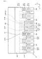
図2〜図4に示すごとく、電力変換装置1は、正極配線を構成する正極バスバー4Pと、負極配線を構成する負極バスバー4Nと、を有する。
図5に示すごとく、第1半導体モジュール2Pと第2半導体モジュール2Nと第3半導体モジュール2Sとを含む複数の半導体モジュールは、互いに積層配置されて積層部3を構成している。
As shown in FIGS. 2 to 4, the
As shown in FIG. 5, a plurality of semiconductor modules including the
図2〜図4に示すごとく、複数の半導体モジュール2P、2N、2Sのそれぞれは、積層部3の積層方向Xに直交する縦方向Zの一方に、複数のパワー端子21を突出してなる。
図2、図6に示すごとく、正極バスバー4P及び負極バスバー4Nは、縦方向Zから見たとき、パワー端子21との接続部に対して横方向Yの一方側に、互いに対向配置されたバスバー本体部41を配置している。ここで、横方向Yとは、積層方向X及び縦方向Zの双方に直交する方向をいう。なお、図6においては、負極バスバー4N及び後述する出力バスバー4O、リアクトルバスバー4Rを省略してある。
As shown in FIGS. 2 to 4, each of the plurality of
As shown in FIGS. 2 and 6, the positive
正極バスバー4P及び負極バスバー4Nは、半導体モジュール2P、2N、2Sとコンデンサ53とを接続する。コンデンサ53は、上述の平滑コンデンサ531及びフィルタコンデンサ532を備える。コンデンサ53は、積層部3に対して、横方向Yの一方側に配されている。正極バスバー4P及び負極バスバー4Nは、パワー端子21に接続される接続部よりも、横方向Yにおける一方側に、バスバー本体部41を有する。本実施形態においては、バスバー本体部41は、横方向Yにおける積層部3とコンデンサ53との間に配されている。
The positive
図5〜図7に示すごとく、複数のパワー端子21のうち、出力配線に接続される出力端子21Oが、横方向Yにおいて最もバスバー本体部41から遠い側に配置されている。
複数のパワー端子21のうち、正極バスバー4Pに接続される正極端子21P又は負極バスバー4Nに接続される負極端子21Nが、横方向Yにおいて最もバスバー本体部41に近い側に配置されている。本実施形態においては、正極端子21Pが、横方向Yにおいて最もバスバー本体部41に近い側に配置されている。
As shown in FIGS. 5 to 7, among the plurality of
Among the plurality of
ここで、第3半導体モジュール2Sにおける最もバスバー本体部41に近い側に配されたパワー端子21を基準端子21Bとする。本実施形態においては、この基準端子21Bとなるパワー端子21は、正極端子21Pである。
Here, the
第1半導体モジュール2Pの正極端子21Pと、第2半導体モジュール2Nの負極端子21Nとのうち、基準端子21Bと電位の異なるパワー端子21は、横方向Yにおいて、基準端子21Bと同じ位置、又はそれよりもバスバー本体部41から遠い位置に配置されている。
Of the
本実施形態においては、上述のように、基準端子21Bが正極端子21Pなので、これと電位が異なるパワー端子21、すなわち第2半導体モジュール2Nの負極端子21Nが、横方向Yにおいて、基準端子21Bと同じ位置、又はそれよりもバスバー本体部41から遠い位置に配置されている。
In the present embodiment, as described above, since the
ただし、本実施形態においては、第1半導体モジュール2Pの正極端子21Pも、横方向Yにおいて、第2半導体モジュール2Nの負極端子21Nと同じ位置に配されている。さらには、本実施形態においては、第2半導体モジュール2Nの負極端子21Nは、基準端子21Bよりも、バスバー本体部41から遠い位置に配されている。これに伴い、第1半導体モジュール2Pの正極端子21Pも、基準端子21Bよりもバスバー本体部41から遠い位置に配されている。
However, in the present embodiment, the
図5に示すごとく、積層部3は、複数の第1半導体モジュール2Pと複数の第2半導体モジュール2Nと複数の第3半導体モジュール2Sとを積層してなる。また、昇圧回路部100を構成する半導体モジュールも、第1のインバータ回路部101を構成する半導体モジュールも、第2のインバータ回路部102を構成する半導体モジュールも、一直線状に積層されている。なお、図示を省略したが、積層方向Xに隣り合う半導体モジュール同士の間には、冷却管が介在している。冷却管は、半導体モジュール2P、2N、2Sの両主面に配され、両主面から冷却するよう構成されている。
As shown in FIG. 5, the
積層部3において、第1のインバータ回路部101を構成する3個の第3半導体モジュール2Sは、互いに連続して積層されている。そして、これらの第3半導体モジュール2Sに対して、積層方向Xにおける一方に、第2のインバータ回路部102を構成する6個の半導体モジュール2P、2Nが積層されている。これら6個の半導体モジュールは、第1半導体モジュール2Pと第2半導体モジュール2Nとである。そして、第1半導体モジュール2Pと第2半導体モジュール2Nとが交互に積層されている。また、第3半導体モジュール2Sに対して積層方向Xの他方には、昇圧回路部100を構成する4個の半導体モジュール2P、2Nが配置されている。これら4個の半導体モジュールについても、第1半導体モジュール2Pと第2半導体モジュール2Nとが交互に積層されている。
In the stacking
昇圧回路部100を構成する半導体モジュール2P、2Nは、図7に示すごとく、リアクトル54との接続配線となるリアクトルバスバー4Rに接続される、中電位端子21Rを有する。つまり、昇圧回路部100における第1半導体モジュール2Pは、パワー端子21として、正極端子21Pと中電位端子21Rとを有する。また、昇圧回路部100における第2半導体モジュール2Nは、パワー端子21として、負極端子21Nと中電位端子21Rとを有する。
As shown in FIG. 7, the
また、横方向Yにおいて、第1半導体モジュール2Pにおける出力端子21Oと、第2半導体モジュール2Nにおける出力端子21Oとは、第3半導体モジュール2Sにおける出力端子21Oと同じ位置、又はそれよりもバスバー本体部41に近い位置に配置されている。本実施形態においては、第1半導体モジュール2Pにおける出力端子21Oと、第2半導体モジュール2Nにおける出力端子21Oとは、第3半導体モジュール2Sにおける出力端子21Oよりもバスバー本体部41に近い位置に配置されている。
In the lateral direction Y, the output terminal 21O in the
図7に示すごとく、出力端子21Oには、回転電機521、522への出力配線を構成する出力バスバー4Oが接続される。この出力バスバー4Oは、出力端子21Oに対して、横方向Yにおける、バスバー本体部41と反対側へ延びるように配されている。図8に示すごとく、出力バスバー4Oは、縦方向Zを向く主面を有する基板部451と、基板部451から縦方向Zに立ち上がる一対の立設部452とを有する。図7に示すごとく、基板部451が、横方向Yにおける、バスバー本体部41と反対側へ延びている。立設部452に、出力端子21Oが接続されている。
As shown in FIG. 7, the output terminal 21O is connected to the output bus bar 4O that constitutes the output wiring to the rotary
また、図7に示すごとく、昇圧回路部100を構成する半導体モジュール2P、2Nにおける中電位端子21Rには、リアクトルバスバー4Rが接続される。リアクトルバスバー4Rも、中電位端子21Rに対して、横方向Yにおける、バスバー本体部41と反対側へ延びるように配されている。また、リアクトルバスバー4Rも、出力バスバー4Oと略同様の形状を有する。すなわち、リアクトルバスバー4Rも、図8に示すごとく、基板部451と一対の立設部452とを有する。立設部452に、中電位端子21Rが接続されている。
Further, as shown in FIG. 7, the
また、複数の出力バスバー4Oとリアクトルバスバー4Rとは、樹脂部43によって互いに絶縁されつつ一体化されている。そして、樹脂部43には、図示を省略した電流センサが設けてある。電流センサとしては、出力バスバー4Oに流れる電流を検出するものと、リアクトルバスバー4Rに流れる電流を検出するものとがある。
Further, the plurality of output bus bars 4O and the
図9に示すごとく、第1半導体モジュール2P及び第2半導体モジュール2Nのそれぞれは、モジュール本体部20と、モジュール本体部20から縦方向Zの一方に突出した2本のパワー端子21とを有する。積層方向Xから見たとき、2本のパワー端子21は、横方向Yにおける中央を通る中心線Cに対して、両側に分かれて配置されている。
As shown in FIG. 9, each of the
第1半導体モジュール2Pと第2半導体モジュール2Nとは、互いに同じ構造を有する。そして、同じ構造の半導体モジュールを、互いに、中心線Cを軸に180°反転させた状態にて積層されている。第1半導体モジュール2Pと第2半導体モジュール2Nとは、内部構造についても、外観形状についても、同様の構造を有する。
The
つまり、いわゆる品番の同じ半導体モジュールを、第1半導体モジュール2P及び第2半導体モジュール2Nとして用いている。そして、積層部3において、第1半導体モジュール2Pと第2半導体モジュール2Nとを積層するにあたっては、両者を、互いに中心線Cを中心軸として反転させた状態で、積層する。こうすることにより、横方向Yにおいて、出力端子21Oとして利用されるパワー端子21が、同じ側に配されることとなる。
That is, semiconductor modules having the same so-called product number are used as the
つまり、第1半導体モジュール2P及び第2半導体モジュール2Nは、いずれも、スイッチング素子を並列接続したものである。そして、一方のパワー端子21が、スイッチング素子のコレクタにつながっており、他方のパワー端子21が、スイッチング素子のエミッタにつながっている。
That is, both the
それゆえ、同じ構造の2つの半導体モジュールを同じ向きで積層配置した場合、コレクタにつながるパワー端子21とエミッタにつながるパワー端子21とが、横方向Yにおける同じ側に配置される。一方、第1半導体モジュール2Pの出力端子21Oは、上アームスイッチング素子20uのエミッタにつながるパワー端子21とする必要がある。第2半導体モジュール2Nの出力端子21Oは、下アームスイッチング素子20dのコレクタにつながるパワー端子21とする必要がある。そのため、同じ構造の2つの半導体モジュールを同じ向きで積層配置して、第1半導体モジュール2P及び第2半導体モジュール2Nとすると、出力端子21Oとすべきパワー端子21が、横方向Yにおける同じ側に配置されない。
Therefore, when two semiconductor modules having the same structure are stacked in the same direction, the
そこで、同じ構造の2つの半導体モジュールについて、一方の半導体モジュールを、中心線Cを軸に反転させた姿勢にて他方の半導体モジュールに対向配置させる。これにより、エミッタに接続されたパワー端子21とコレクタに接続されたパワー端子21とを横方向Yにおける同じ側に配置される。つまり、第1半導体モジュール2Pの出力端子21Oと第2半導体モジュール2Nの出力端子21Oとが、横方向Yにおける同じ側に配置される。
Therefore, with respect to the two semiconductor modules having the same structure, one semiconductor module is arranged to face the other semiconductor module in a posture in which the center line C is inverted. As a result, the
このような配置は、昇圧回路部100においても、同様に行われている。つまり、中電位端子21Rが、横方向Yにおける同じ側に配されるように、第1半導体モジュール2Pと第2半導体モジュール2Nとが積層されている。すなわち、同じ構造の半導体モジュールにて、第1半導体モジュール2Pと第2半導体モジュール2Nとを構成するにあたり、一方を他方に対して、中心線Cを軸に反転させて、積層している。
Such an arrangement is similarly performed in the
上記の第2のインバータ回路部102を構成する半導体モジュールと同様に、第1半導体モジュール2Pにおけるエミッタにつながるパワー端子21と、第2半導体モジュール2Nにおけるコレクタにつながるパワー端子21とが、それぞれ中電位端子21Rとなる。それゆえ、上記のような反転させた積層の仕方をすることにより、中電位端子21Rを、横方向Yにおける同じ側に配置することができる。
Similar to the semiconductor module forming the second
また、第1半導体モジュール2P及び第2半導体モジュール2Nは、それぞれ中心線Cを対称軸として線対称となる位置に、2つのパワー端子21を設けている。また、第1半導体モジュール2P及び第2半導体モジュール2Nは、パワー端子21の突出側と反対側へ複数の制御端子22を突出形成してなる。本実施形態において、第1半導体モジュール2P及び第2半導体モジュール2Nは、それぞれ、制御端子22も含めて、中心線Cを対称軸とした線対称の形状を有する。
Further, the
図5に示すごとく、第1半導体モジュール2Pの正極端子21Pと、第2半導体モジュール2Nの負極端子21Nとは、互いに積層方向Xに対向配置されている。つまり、積層方向Xから見たとき、これらの正極端子21Pと負極端子21Nとが重なっている。特に、本実施形態においては、縦方向Zから見たとき、第1半導体モジュール2Pの正極端子21Pと第2半導体モジュール2Nの負極端子21Nとが、積層方向Xに沿って一直線状に配列されている。
As shown in FIG. 5, the
第1半導体モジュール2P及び第2半導体モジュール2Nの出力端子21Oは、互いに積層方向Xに対向配置されている。つまり、積層方向Xから見たとき、これらの出力端子21Oが重なっている。特に、本実施形態においては、縦方向Zから見たとき、第1半導体モジュール2P及び第2半導体モジュール2Nの出力端子21Oが、積層方向Xに沿って一直線状に配列されている。
The output terminals 21O of the
また、昇圧回路部100を構成する第1半導体モジュール2P及び第2半導体モジュール2Nの中電位端子21Rも、互いに積層方向Xに対向配置されている。また、本実施形態においては、第2のインバータ回路部102を構成する半導体モジュール2P、2Nにおける出力端子21Oと、昇圧回路部100を構成する半導体モジュール2P、2Nにおける中電位端子21Rとは、積層方向Xに沿って一直線状に配列されている。
In addition, the medium
また、昇圧回路部100を構成する半導体モジュール2P、2Nと、第2のインバータ回路部102を構成する半導体モジュール2P、2Nとの間において、これらの正極端子21Pと負極端子21Nとが、積層方向Xに沿って一直線状に配列されている。
なお、本実施形態においては、第1のインバータ回路部101を構成する第3半導体モジュール2Sのパワー端子21は、昇圧回路部100におけるパワー端子21に対しても、第2のインバータ回路部102におけるパワー端子21に対しても、横方向Yにおける位置が揃っていない。
Further, between the
In addition, in the present embodiment, the
図10、図11に示すごとく、電力変換装置1は、スイッチング回路部を駆動する駆動回路を備えた回路基板11を有する。第1半導体モジュール2P、第2半導体モジュール2N、及び第3半導体モジュール2Sは、それぞれ、回路基板11と反対側にパワー端子21を突出してなる。すなわち、回路基板11は、積層部3に対して、縦方向Zにおける、パワー端子21の突出側と反対側に配置されている。そして、回路基板11の主面が、積層部3に、縦方向Zから対向している。
As shown in FIGS. 10 and 11, the
図9〜図11に示すごとく、半導体モジュール2P、2N、2Sは、モジュール本体部20から、複数の制御端子22を突出してなる。制御端子22は、Z方向における、パワー端子21と反対側に突出している。これらの制御端子22が、回路基板11に接続されている。制御端子22のうちの一部は、半導体モジュールにおけるスイッチング素子20u、20dのゲートに電気的に接続されている。
As shown in FIGS. 9 to 11, each of the
次に、本実施形態の作用効果につき説明する。
上記電力変換装置1は、第1半導体モジュール2Pと、第2半導体モジュール2Nと、第3半導体モジュール2Sとを有する。これにより、電力変換装置1における低損失、小型化、低コスト化を実現しやすい。
Next, the function and effect of this embodiment will be described.
The
まず、第1半導体モジュール2P、第2半導体モジュール2N、第3半導体モジュール2Sは、それぞれ複数のスイッチング素子を集約して内蔵している。そのため、電力変換装置1の小型化、低コスト化を実現しやすい。
First, each of the
また、電力変換装置1において、流れる電流量が比較的大きいアームには、第1半導体モジュール2P又は第2半導体モジュール2Nを用いることで、大電流に備えることができる。それとともに、第1半導体モジュール2P及び第2半導体モジュール2Nは、それぞれ、並列接続された複数のスイッチング素子を内蔵している。そのため、各半導体モジュール2P、2N内において並列接続されたスイッチング素子の間の接続配線を短くすることができる。その結果、この接続配線におけるインダクタンスを低減することができる。これにより、スイッチング損失を低減することができる。なお、この点については、後述する比較形態を参照されたい。
Further, in the
また、流れる電流量が比較的小さいアームには、第3半導体モジュール2Sを用いることで、電力変換装置1における半導体モジュールの数を少なくすることができる。その結果、電力変換装置1の小型化、低コスト化を実現することができる。
In addition, the number of semiconductor modules in the
このように、電力変換装置1は、第1半導体モジュール2Pと第2半導体モジュール2Nと第3半導体モジュール2Sとを有することにより、低損失、小型化、低コスト化を実現しやすくなる。
As described above, the
第1半導体モジュール2Pの負極端子21Nは、基準端子21Bである第3半導体モジュール2Sの正極端子21Pよりも、バスバー本体部41から遠い位置に配置されている。すなわち、第1半導体モジュール2Pの正極端子21Pと、第2半導体モジュール2Nの負極端子21Nとのうち、基準端子21Bと電位の異なるパワー端子21は、横方向Yにおいて、基準端子21Bと同じ位置、又はそれよりもバスバー本体部41から遠い位置に配置されているということとなる。これにより、バスバー4を介した同電位の複数のパワー端子21の間の電流経路の距離を短くすることができる。
The
つまり、例えば、図12に示すごとく、基準端子21Bと電位の異なるパワー端子21(例えば負極端子21N)が、横方向Yにおいて、基準端子21Bよりもバスバー本体部41に近い場合を想定する。この場合、当該パワー端子21(ここでは負極端子21N)を避けるように基準端子21Bと同電位のバスバー(ここでは正極バスバー4P)を形成したとき、同電位のパワー端子21(ここでは正極端子21P)の間の電流経路が長くなりやすい。これに対して、図7に示す本実施形態のようなパワー端子21の配置とすることで、バスバー(本実施形態においては、正極バスバー4P)を介したパワー端子21(本実施形態においては、正極端子21P)間の電流経路の距離が長くなることを防ぐことができる。
That is, for example, as illustrated in FIG. 12, it is assumed that the power terminal 21 (for example, the
本実施形態においては、上述のように、第1半導体モジュール2Pの負極端子21Nが、基準端子21Bである第3半導体モジュール2Sの正極端子21Pよりも、バスバー本体部41から遠い位置に配置されている。これにより、正極バスバー4Pを介した正極端子21Pの間の電流経路の距離を、一層短くすることができる。
In the present embodiment, as described above, the negative terminal 21N of the
また、横方向Yにおいて、第1半導体モジュール2P及び第2半導体モジュール2Nにおける出力端子21Oは、第3半導体モジュール2Sにおける出力端子21Oと同じ位置、又はそれよりもバスバー本体部41に近い位置に配置されている。それゆえ、第1半導体モジュール2P及び第2半導体モジュール2Nに接続される出力バスバー4Oの全体を、積層部3における横方向Yの中央側に近付けやすくなる。その結果、横方向Yにおける電力変換装置1の小型化を実現しやすい。
Further, in the lateral direction Y, the output terminals 21O of the
すなわち、第1半導体モジュール2P及び第2半導体モジュール2Nにおける出力端子21Oが、第3半導体モジュール2Sにおける出力端子21Oよりもバスバー本体部41から遠い位置に配置されている場合を想定する。この場合、第1半導体モジュール2P及び第2半導体モジュール2Nに接続される出力バスバー4Oの全体が、第3半導体モジュール2Sに接続される出力バスバー4Oよりも、積層部3の中央から遠い位置に配されるおそれがある。そうすると、横方向Yにおける電力変換装置1の体格が大きくなるおそれがある。これに対して、第1半導体モジュール2P及び第2半導体モジュール2Nにおける出力端子21Oの配置を本実施形態のようにすることにより、電力変換装置1の小型化を図りやすい。
That is, it is assumed that the output terminals 21O of the
特に、本実施形態においては、第1半導体モジュール2P及び第2半導体モジュール2Nにおける出力端子21Oは、第3半導体モジュール2Sにおける出力端子21Oよりもバスバー本体部41に近い位置に配置されている。それゆえ、横方向Yにおける電力変換装置1の小型化を一層図りやすい。すなわち、この場合には、例えば、第1半導体モジュール2P及び第2半導体モジュール2Nにおける出力端子21Oの寸法公差等を考慮しても、これらに接続される出力バスバー4Oが横方向Yにおいて積層部3の中央から遠ざかりにくい。その結果、上記寸法公差等を考慮しても、電力変換装置1の小型化を図りやすい。
In particular, in the present embodiment, the output terminals 21O of the
第1半導体モジュール2P及び第2半導体モジュール2Nは、積層方向Xから見たとき、2本のパワー端子21が中心線Cに対して、両側に分かれて配置されている。これにより、第1半導体モジュール2P及び第2半導体モジュール2Nの質量バランスを、横方向Yにおいて取りやすい。それゆえ、積層部3の耐振動性を向上させやすい。
In the
第1半導体モジュール2Pと第2半導体モジュール2Nとは、互いに同じ構造を有する。そして、同じ構造の半導体モジュールを、互いに、中心線Cを軸に反転させた状態にて積層されている。これにより、電力変換装置1の低コスト化を図ることができる。すなわち、第1半導体モジュール2Pと第2半導体モジュール2Nとを、異なる構造の半導体モジュールにて構成する場合に比べ、コスト低減を図ることができる。また、同じ構造の半導体モジュールを互いに反転させて、第1半導体モジュール2Pと第2半導体モジュール2Nとすることで、上述のように、出力端子21O同士を近接配置することができる。同様に、正極端子21Pと負極端子21Nとを、横方向Yにおける同じ側に配することができる。その結果、正極バスバー4P、負極バスバー4N、及び出力バスバー4Oと、半導体モジュール2P、2N、2Sとの接続構造を簡素化することができる。
The
第1半導体モジュール2Pの正極端子21Pと、第2半導体モジュール2Nの負極端子21Nとは、互いに積層方向Xに対向配置されている。これにより、互いに対向配置された正極端子21Pと負極端子21Nとの間においてインダクタンスを低減することができる。その結果、スイッチング回路部のインダクタンスの低減を図ることができる。
The
第1半導体モジュール2P及び第2半導体モジュール2Nの出力端子21Oは、互いに積層方向Xに対向配置されている。これにより、互いに対向配置された一対の出力端子21Oの間においてインダクタンスを低減することができる。その結果、スイッチング回路部のインダクタンスの低減を図ることができる。
The output terminals 21O of the
第1半導体モジュール2P、第2半導体モジュール2N、及び第3半導体モジュール2Sは、それぞれ、回路基板11と反対側にパワー端子21を突出してなる。すなわち、回路基板11は、積層部3に対して、縦方向Zにおける、パワー端子21の突出側と反対側に配置されている。これにより、パワー端子21及びこれに接続されるバスバーに流れる電流によるノイズの影響が、回路基板11に影響することを抑制することができる。
Each of the
特に、第1半導体モジュール2P及び第2半導体モジュール2Nの出力端子21Oに接続される出力バスバー4Oに流れる電流iの経路は、図13に示すごとく、横方向Yに沿う向きのみならず、積層方向Xに沿う向きにも存在する。それゆえ、仮に、出力バスバー4Oと同じ側に、回路基板11が配されていると、回路基板11における配線の向きを工夫しても、ノイズの影響を防ぐことが困難である。それゆえ、回路基板11を、積層部3を挟んで、縦方向Zの反対側に配することで、回路基板11へのノイズの影響を効果的に抑制することができる。
In particular, the path of the current i flowing through the output bus bar 4O connected to the output terminals 21O of the
以上のごとく、本実施形態によれば、低損失、小型化、低コスト化を容易にすることができる電力変換装置を提供することができる。 As described above, according to the present embodiment, it is possible to provide a power conversion device that can facilitate low loss, downsizing, and cost reduction.
(実施形態2)
本実施形態は、図14に示すごとく、横方向Yにおける両端に配された2つのパワー端子21を、複数の半導体モジュール2P、2N、2Sにおいて、横方向Yにおける同じ位置に配置した、電力変換装置1の形態である。
(Embodiment 2)
According to the present embodiment, as shown in FIG. 14, two
すなわち、図14に示すごとく、第1半導体モジュール2Pの正極端子21Pと、第2半導体モジュール2Nの負極端子21Nとを、基準端子21Bである第3半導体モジュール2Sの正極端子21Pと、横方向Yにおける同じ位置に配置している。そして、これら第1半導体モジュール2Pの正極端子21Pと、第2半導体モジュール2Nの負極端子21Nと、第3半導体モジュール2Sの正極端子21Pとが、積層方向Xに沿って一直線状に並んでいる。
That is, as shown in FIG. 14, the positive terminal 21P of the
また、第1半導体モジュール2Pの出力端子21Oと、第2半導体モジュール2Nの出力端子21Oとを、第3半導体モジュール2Sの出力端子21Oと、横方向Yにおける同じ位置に配置している。そして、これら第1半導体モジュール2Pの出力端子21Oと、第2半導体モジュール2Nの出力端子21Oと、第3半導体モジュール2Sの出力端子21Oとが、積層方向Xに沿って一直線状に並んでいる。
Further, the
また、複数の半導体モジュールは、複数のパワー端子21における横方向Yの端縁のうち、少なくとも、互いに反対側を向く2つの端縁(211、212、215、216)が、積層方向Xに重なるように配置されている。
Further, in the plurality of semiconductor modules, at least two edges (211, 212, 215, 216) of the plurality of
特に、本実施形態においては、第1半導体モジュール2Pの正極端子21Pと、第2半導体モジュール2Nの負極端子21Nと、第3半導体モジュール2Sの正極端子21Pとが、それぞれの横方向Yにおける両側の端縁211、212において、積層方向Xに重なるように配置されている。さらに、第1半導体モジュール2Pの出力端子21Oと、第2半導体モジュール2Nの出力端子21Oと、第3半導体モジュール2Sの出力端子21Oとが、それぞれの横方向Yにおける両側の端縁215、216において、積層方向Xに重なるように配置されている。
Particularly, in the present embodiment, the
その他の構成は、実施形態1と同様である。なお、実施形態2以降において用いた符号のうち、既出の実施形態において用いた符号と同一のものは、特に示さない限り、既出の実施形態におけるものと同様の構成要素等を表す。 Other configurations are similar to those of the first embodiment. In addition, among the reference numerals used in the second and subsequent embodiments, the same reference numerals as those used in the already-described embodiments represent the same components and the like as those in the already-described embodiments, unless otherwise specified.
本実施形態においては、第1半導体モジュール2Pの正極端子21Pと第2半導体モジュール2Nの負極端子21Nとの双方が、横方向Yにおいて、基準端子21Bと同じ位置に配置されている。したがって、第1半導体モジュール2Pの正極端子21Pと、第2半導体モジュール2Nの負極端子21Nとのうち、基準端子21Bと電位の異なるパワー端子21は、横方向Yにおいて、基準端子21Bと同じ位置に配置されていることとなる。それゆえ、上記実施形態1にて説明したように、同電位のパワー端子21の間の電流経路の距離を短くしやすい。
In the present embodiment, both the
また、本実施形態においては、横方向Yにおいて、第1半導体モジュール2P及び第2半導体モジュール2Nにおける出力端子21Oが、第3半導体モジュール2Sにおける出力端子21Oと同じ位置に配置されている。それゆえ、上記実施形態1において説明したように、電力変換装置1の小型化を図りやすい。
Further, in the present embodiment, the output terminals 21O in the
また、複数の半導体モジュールは、複数のパワー端子21における横方向Yの端縁のうち、少なくとも、互いに反対側を向く2つの端縁211、212、215、216が、積層方向Xに重なるように配置されている。それゆえ、積層部3に複数の半導体モジュールを組み付ける際、横方向Yにおける位置決めを正確に行いやすい。すなわち、積層部3に半導体モジュールを組み付けるにあたっては、図15に示すごとく、位置決め治具6を用いる。
In addition, in the plurality of semiconductor modules, at least two
つまり、図15に示すごとく、位置決め治具6は、電力変換装置1のケースを縦方向Zにおいて支承するケース支承部61と、半導体モジュールを縦方向Zから支承するモジュール支承部62と、半導体モジュールを横方向Yに位置決めする位置決め部63とを有する。図15に示す位置決め治具6においては、一部のモジュール支承部62と一部の位置決め部63とが、共通している。位置決め部63は、図16に示すごとく、積層方向Xに延びるように直線状に形成されている。
That is, as shown in FIG. 15, the
この位置決め治具6に、ケース12と複数の半導体モジュール2P、2N、2Sとを、冷却器13等と共に配置する。このとき、複数の半導体モジュール2P、2N、2Sにおけるパワー端子21の端縁211、212を、位置決め部63に、横方向Yから当接させる。すなわち、一対の位置決め部63の間に、パワー端子21を挿入すると共に、その一対の端縁211、212を、横方向Yに当接させる。これにより、この端縁211、212を基準に、位置決め治具6に対して複数の半導体モジュール2P、2N、2Sが、横方向Yに位置決めされる。位置決め部63は、積層方向Xに一直線状に形成されているため、複数の半導体モジュール2P、2N、2Sのパワー端子21も、積層方向Xに一直線状に配列される。
The
なお、位置決め部63に当接させるパワー端子21の一対の端縁は、互いに横方向Yの反対側を向くものであればよい。すなわち、位置決め用の一対の端縁としては、出力端子21Oの一対の端縁215、216を用いてもよいし、横方向Yの両端のパワー端子21の外側の端縁211、216を用いてもよい。或いは、一対の端縁として、横方向Yの両端のパワー端子21の内側の端縁212、215を用いてもよい。もちろん、それに対応して、位置決め部63の位置を変えることとなる。
It should be noted that the pair of edges of the
上記のように、複数の半導体モジュール2P、2N、2Sの横方向Yにおける位置決めを容易に行うことができる。また、複数の半導体モジュールのパワー端子21が積層方向Xに一直線状に並ぶことで、パワー端子21とバスバーとの接続作業を容易に行うことができる。例えば、これらの接続を、溶接によって行う場合等において、その作業を容易に行うことができる。その結果、電力変換装置1の生産性を向上させることができる。
その他、実施形態1と同様の作用効果を有する。
As described above, the positioning of the plurality of
Other than that, the same effects as those of the first embodiment are obtained.
(実施形態3)
本実施形態においては、図17に示すごとく、横方向Yにおけるパワー端子21の配列及び幅のバリエーションを示す。
本実施形態においても、複数の半導体モジュール2P、2N、2Sが、複数のパワー端子21における横方向Yの端縁のうち、少なくとも、互いに反対側を向く2つの端縁が積層方向Xに重なるように、配置される。図17に示した一点鎖線は、当該一点鎖線に沿った端縁が、複数の半導体モジュール2P、2N、2Sの間において、積層方向Xに重なることを意味する。以降の同種の図面においても同様である。
(Embodiment 3)
In the present embodiment, as shown in FIG. 17, variations in the arrangement and width of the
Also in the present embodiment, in the plurality of
図17に示すごとく、第1半導体モジュール2P、第2半導体モジュール2N、第3半導体モジュール2Sのいずれもが、3つのパワー端子21を有する。そして、3つのパワー端子21の横方向Yの位置及び幅が、積層部3を構成する複数の半導体モジュール2P、2N、2Sの何れにおいても同じである。それゆえ、3つのパワー端子21における横方向Yの端縁は、すべて、複数の半導体モジュール2P、2N、2Sの間で重なる。したがって、これらの端縁のうち、互いに反対側を向く2つの端縁において、複数の半導体モジュールの横方向Yにおける位置決めを行うことができる。
As shown in FIG. 17, each of the
例えば、実施形態2の図15、図16にて示した位置決め治具6のように、各半導体モジュールにおける一つのパワー端子21の一対の端縁211、212において、位置決めを行うことができる。他の端縁213〜216を適宜用いて位置決めを行うこともできる。
For example, like the
なお、第1半導体モジュール2P及び第2半導体モジュール2Nにおける3本のパワー端子21は、いずれか1本又は2本がコレクタに接続されており、残りのパワー端子21がエミッタに接続されたものとすることができる。また、3本のパワー端子21のうち、横方向Yにおける両側に配されたパワー端子21が、同電位のパワー端子21となる。それゆえ、第1半導体モジュール2P及び第2半導体モジュール2Nにおける3本のパワー端子21のうち、出力端子21Oとなるパワー端子21は、横方向Yにおける両端の2本か、中央の1本かのいずれかとなる。
その他は、実施形態2と同様の構成および作用効果を有する。
It should be noted that one or two of the three
Others have the same configurations and effects as those of the second embodiment.
(実施形態4)
本実施形態は、図18、図19に示すごとく、横方向Yにおける両端の2つのパワー端子21における、外側の端縁211、216を、複数の半導体モジュール2P、2N、2Sの間で揃えた形態である。
(Embodiment 4)
In this embodiment, as shown in FIGS. 18 and 19, the
つまり、第1半導体モジュール2P及び第2半導体モジュール2Nについては、2つのパワー端子21における横方向Yの外側を向く一対の端縁211、216を、位置決め用の端縁とする。また、第3半導体モジュール2Sについては、3つのパワー端子21のうち、横方向Yにおける両端のパワー端子21における外側を向く一対の端縁211、216を、位置決め用の端縁とする。
That is, regarding the
これにより、図19に示すごとく、これらの端縁211、216を、位置決め治具6の一対の位置決め部63にそれぞれ当接させることで、複数の半導体モジュールの横方向Yにおける位置決めを行うことができる。
また、第1半導体モジュール2P及び第2半導体モジュール2Nにおけるパワー端子21は、横方向Yの幅が第3半導体モジュール2Sにおけるパワー端子21よりも大きい。これにより、第1半導体モジュール2P及び第2半導体モジュール2Nのパワー端子21におけるインダクタンスをより低減することができる。
その他は、実施形態2と同様の構成および作用効果を有する。
As a result, as shown in FIG. 19, the end edges 211 and 216 are brought into contact with the pair of
Further, the width of the
Others have the same configurations and effects as those of the second embodiment.
(実施形態5)
本実施形態は、図20に示すごとく、横方向Yにおける一端のパワー端子21における、2つの端縁211、212を、複数の半導体モジュール2P、2N、2Sの間で揃えた形態である。
すなわち、例えば、第1半導体モジュール2Pの正極端子21Pと、第2半導体モジュール2Nの負極端子21Nと、第3半導体モジュール2Sの正極端子21Pとを、横方向Yの同じ位置に設けると共に、その幅を同じにしている。
(Embodiment 5)
In the present embodiment, as shown in FIG. 20, the two
That is, for example, the
これにより、図21に示すごとく、各半導体モジュールの一つのパワー端子21の一対の端縁211、212を、一対の位置決め部63にて挟持するように、位置決めすることができる。
Thereby, as shown in FIG. 21, the pair of
また、第1半導体モジュール2P及び第2半導体モジュール2Nにおける出力端子21O又は中電位端子21Rとなるパワー端子21は、横方向Yの幅を大きくしてある。
Moreover, the width of the
また、図22に示すごとく、第1半導体モジュール2P及び第2半導体モジュール2Nにおける出力端子21O又は中電位端子21Rとなるパワー端子21を、横方向Yにおける同じ位置に、同じ幅にて形成した構成とすることもできる。この場合、出力端子21O又は中電位端子21Rの一対の端縁215、216を、位置決め用の端縁とすることができる。
In addition, as shown in FIG. 22, a configuration in which the
また、第1半導体モジュール2Pにおける正極端子21P及び第2半導体モジュール2Nにおける負極端子21Nについて、横方向Yの幅を大きくしてある。この図22に示す構成は、図20に示した構成と、横方向Yにおいて反転させた態様である。
その他は、実施形態2と同様の構成および作用効果を有する。
In addition, the width of the
Others have the same configurations and effects as those of the second embodiment.
(実施形態6)
本実施形態は、図23に示すごとく、第3半導体モジュール2Sにおける隣り合う2本のパワー端子21の、互いに反対側を向く端縁211、214を、位置決め用の端縁とした形態である。
これに伴い、第1半導体モジュール2P及び第2半導体モジュール2Nにおいては、2本のパワー端子21の互いに反対側を向く端縁211、214を、位置決め用の端縁とする。
(Embodiment 6)
In the present embodiment, as shown in FIG. 23, the
Along with this, in the
例えば、図23に示すごとく、第3半導体モジュール2Sの正極端子21Pと負極端子21Nとにおける、互いに反対側を向く端縁211、214を、位置決め用の端縁とする。また、第1半導体モジュール2Pについては、正極端子21Pと出力端子21Oとにおける、互いに横方向Yの外側を向く端縁211、214を、位置決め用の端縁とする。さらに、第2半導体モジュール2Nについては、負極端子21Nと出力端子21Oとにおける、互いに横方向Yの外側を向く端縁211、214を、位置決め用の端縁とする。
For example, as shown in FIG. 23, the
これにより、図24に示すごとく、2本のパワー端子21を、位置決め治具6の一対の位置決め部63によって、横方向Yから挟持させるような状態で、位置決めを行うことができる。
As a result, as shown in FIG. 24, the two
また、図25に示すごとく、第3半導体モジュール2Sにおける、負極端子21Nの一つの端縁213と出力端子21Oにおける一つの端縁216とを、位置決め用の端縁とすることもできる。すなわち、第1半導体モジュール2P及び第2半導体モジュール2Nにおける2本のパワー端子21を、横方向Yにおいて、それぞれ第3半導体モジュール2Sの負極端子21N及び出力端子21Oと同じ位置に、形成することもできる。
Further, as shown in FIG. 25, one
そして、第1半導体モジュール2P及び第2半導体モジュール2Nにおける2本のパワー端子21の互いに横方向Yの外側を向く端縁213、216を、第3半導体モジュール2Sの負極端子21Nの端縁213、及び出力端子21Oの端縁216と同じ位置に配置する。この場合、位置決め治具6は、図24に示すものに対して、左右対称の形とすることができる。
その他は、実施形態2と同様の構成および作用効果を有する。
Then, the
Others have the same configurations and effects as those of the second embodiment.
(実施形態7)
本実施形態は、図26に示すごとく、隣り合う2つのパワー端子21における互いに横方向Yに対向する端縁を、位置決め用の端縁とした形態である。
すなわち、第3半導体モジュール2Sの負極端子21Nの端縁214と、出力端子21Oの端縁215とを、位置決め用の端縁としている。また、第1半導体モジュール2P及び第2半導体モジュール2Nにおける2つのパワー端子21における互いに対向する端縁214、215を、位置決め用の端縁としている。
(Embodiment 7)
In the present embodiment, as shown in FIG. 26, the edges of two
That is, the
すなわち、第1半導体モジュール2Pにおいては、正極端子21Pの端縁214と、これに横方向Yに対向する出力端子21Oの端縁215とが、位置決め用の端縁となる。また、第2半導体モジュール2Nにおいては、負極端子21Nの端縁214と、これに横方向Yに対向する出力端子21Oの端縁215とが、位置決め用の端縁となる。また、第3半導体モジュール2Sにおいては、負極端子21Nの端縁214と、これに横方向Yに対向する出力端子21Oの端縁215とが、位置決め用の端縁となる。
That is, in the
第1半導体モジュール2P及び第2半導体モジュール2Nにおける2つのパワー端子21の間の間隙A2の横方向Yの幅及び位置を、第3半導体モジュール2Sの負極端子21Nと出力端子21Oとの間の間隙A1の横方向Y幅及び位置に、揃えている。
The width and position in the lateral direction Y of the gap A2 between the two
本形態の場合、図27に示すごとく、位置決め治具6の位置決め部63を、上記の2つのパワー端子21の間の間隙A1、A2に嵌入するようにして、複数の半導体モジュールを並べて、横方向Yの位置決めを行うこととなる。
なお、図26に示す形態においては、第1半導体モジュール2P及び第2半導体モジュール2Nにおける正極端子21P又は負極端子21Nの幅を大きくしている。
In the case of this embodiment, as shown in FIG. 27, the plurality of semiconductor modules are arranged side by side so that the
In addition, in the form shown in FIG. 26, the width of the
また、図28に示すごとく、第3半導体モジュール2Sの正極端子21Pと負極端子21Nとの間の間隙A1に面するパワー端子21の端縁212、213を、位置決め用の端縁とすることもできる。この場合、第1半導体モジュール2Pにおける正極端子21P及び第2半導体モジュール2Nの負極端子21Nを、横方向Yにおいて、第3半導体モジュール2Sの正極端子21Pと同じ位置に配置することとなる。そして、第1半導体モジュール2Pの正極端子21P又は第2半導体モジュール2Nの負極端子21Nと、出力端子21O又は中電位端子21Rとの間の間隙A2を、横方向Yにおいて、第3半導体モジュール2Sの正極端子21Pと負極端子21Nとの間の間隙A1と同じ位置に同じ幅にて形成することとなる。
Further, as shown in FIG. 28, the
この場合、位置決め治具6は、図27に示すものに対して、左右対称の形とすることができる。
その他は、実施形態2と同様の構成および作用効果を有する。
In this case, the
Others have the same configurations and effects as those of the second embodiment.
(実施形態8)
本実施形態は、図29、図30に示すごとく、第2半導体モジュール2Nにおける負極端子21Nのみを、基準端子21Bである第3半導体モジュール2Sの正極端子21Pよりも、バスバー本体部41から遠い位置に設けたものである。
なお、図29においては、バスバー本体部41の図示は省略してあるが、図30に示すごとく、積層部3における、出力端子21Oが配された側と反対側に、バスバー本体部41が配されている。
(Embodiment 8)
In the present embodiment, as shown in FIGS. 29 and 30, only the
Although illustration of the bus bar
本実施形態においては、第1半導体モジュール2Pにおける正極端子21Pの位置は、横方向Yにおいて、第3半導体モジュール2Sの正極端子21Pと同じ位置に設けてある。
In the present embodiment, the position of the
本実施形態においては、正極バスバー4Pを、図30に示すように、配置することができる。つまり、第1半導体モジュール2Pの正極端子21Pを、第3半導体モジュール2Sの正極端子21Pと同じ位置に設けてある分、正極バスバー4Pにおける積層部3の中央側の端縁の凹凸形状を小さくすることができる。これにより、正極バスバー4Pを介した正極端子21P同士の電流経路の距離を、より短くすることができる。
その他は、実施形態1と同様の構成および作用効果を有する。
In the present embodiment, the positive
Others have the same configurations and effects as those of the first embodiment.
(実施形態9)
本実施形態においては、図31に示すごとく、第1半導体モジュール2Pの正極端子21P及び第2半導体モジュール2Nの負極端子21Nを、基準端子21Bである第3半導体モジュール2Sの正極端子21Pと、横方向Yにおける同じ位置に設けた形態である。
(Embodiment 9)
In the present embodiment, as shown in FIG. 31, the positive terminal 21P of the
一方、第1半導体モジュール2P及び第2半導体モジュール2Nにおける出力端子21O及び中電位端子21Rは、第3半導体モジュール2Sの出力端子21Oよりも、バスバー本体部41側にある。それゆえ、第1半導体モジュール2P及び第2半導体モジュール2Nに接続される出力バスバー4Oが積層部3に対して、横方向Yの外側に広がりすぎることを抑制することができる。この点は、実施形態1と同様である。
その他、実施形態1と同様の構成および作用効果を有する。
On the other hand, the output terminal 21O and the intermediate
Besides, it has the same configuration and operation effects as those of the first embodiment.
(実施形態10)
本実施形態においては、図32に示すごとく、昇圧回路部100における中電位端子21Rを、横方向Yにおいて、第2のインバータ回路部102における出力端子21Oとは異なる位置に設けた形態である。
本実施形態においては、第1半導体モジュール2P及び第2半導体モジュール2Nの出力端子21Oを、横方向Yにおいて、第3半導体モジュール2Sの出力端子21Oよりも、バスバー本体部41に近い側に配置している。一方、昇圧回路部100における中電位端子21Rを、横方向Yにおいて、第3半導体モジュール2Sの出力端子21Oと略同等の位置に配している。
その他、実施形態1と同様の構成および作用効果を有する。
(Embodiment 10)
In the present embodiment, as shown in FIG. 32, the intermediate
In the present embodiment, the output terminals 21O of the
Besides, it has the same configuration and operation effects as those of the first embodiment.
(比較形態)
本比較形態は、図33に示すごとく、スイッチング回路部のすべてを、第3半導体モジュール2Sにて構成した電力変換装置9の形態である。
つまり、第1のインバータ回路部901のみならず、第2のインバータ回路部902及び昇圧回路部900も、それぞれ複数の第3半導体モジュール2Sにて構成してある。さらに、第2のインバータ回路部902及び昇圧回路部900においては、第3半導体モジュール2Sを並列接続して、一つのレグを構成している。
(Comparison form)
As shown in FIG. 33, the present comparative form is a form of the
That is, not only the first
この場合には、複数の第3半導体モジュール2Sの間の接続配線におけるインダクタンスが生じやすい。図34には、互いに並列接続された2つの第3半導体モジュール2Sの下アーム部分における、配線インダクタンスを記入した等価回路図を示す。同図に示すように、2つの第3半導体モジュール2Sにおける下アームスイッチング素子20dのエミッタ同士が、各第3半導体モジュール2Sの負極端子21Nにおいて互いに接続される。そして、この接続配線90におけるインダクタンスが大きくなりやすい。
In this case, inductance is likely to occur in the connection wiring between the plurality of
ここで、並列接続された2つのスイッチング素子20dの特性公差に起因して、これらに流れる電流にバラツキが生じることもある。そうすると、この電流バラツキと接続配線90におけるインダクタンスとに起因して、各スイッチング素子20dにおけるゲート−エミッタ間電圧が高くなりすぎたり、低くなりすぎたりすることがある。これを防ぐためにスイッチング速度を遅くする必要が生じる。そうすると、スイッチング素子20dにおける損失が大きくなる。その結果、スイッチング素子20dの大型化や高コスト化を招くことになる。なお、上記のような現象は、上アームにおいても生じる。
その結果、電力変換装置9の低損失、小型化、低コスト化を図ることが困難となる。
Here, due to the characteristic tolerance of the two
As a result, it becomes difficult to achieve low loss, downsizing, and cost reduction of the
これに対して、実施形態1等に示す電力変換装置1においては、第1半導体モジュール2P及び第2半導体モジュール2Nを適宜利用することで、上記の課題を解決している。つまり、互いに並列接続されるスイッチング素子を一体化した半導体モジュール2P、2Nを用いることで、並列接続されたスイッチング素子の間の配線インダクタンスを大幅に低減することができる。それゆえ、電力変換装置1の低損失、小型化、低コスト化を実現しやすい。
On the other hand, in the
本発明は上記各実施形態に限定されるものではなく、その要旨を逸脱しない範囲において種々の実施形態に適用することが可能である。 The present invention is not limited to the above-described embodiments, and can be applied to various embodiments without departing from the spirit of the invention.
上記各実施形態においては、昇圧回路部100を設けた形態を示したが、昇圧回路部100を持たない電力変換装置とすることもできる。また、昇圧回路部100を設ける場合において、昇圧回路部100を、第3半導体モジュール2Sにて構成することもできる。この場合、昇圧回路部100は、一つの第3半導体モジュール2Sにて構成してもよいし、複数の第3半導体モジュール2Sを並列接続して用いることもできる。
In each of the above-described embodiments, the mode in which the
また、第1半導体モジュール2P及び第2半導体モジュール2Nは、異なる種類の半導体素子を並列接続したものとすることもできる。例えば、一つの半導体モジュールに、SiC−MOSFETとSi−IGBTとを並列接続してもよい。SiC−MOSFETは、SiC(すなわち、炭化シリコン)によって形成されるMOSFETである。また、Si−IGBTは、Si(すなわち、シリコン)によって形成されるIGBTである。さらには、スイッチング素子として、Si−RCIGBTを用いることもできる。RCIGBTは、還流ダイオードをIGBTと一体化した半導体素子である。
Further, the
また、第1半導体モジュール2P及び第2半導体モジュール2Nは、2個のスイッチング素子を並列接続したものに限らず、3個以上のスイッチング素子を並列接続したものとしてもよい。
Further, the
また、例えば、第3半導体モジュールにおけるパワー端子の並びについては、特に限定されるものではない。例えば、正極端子を横方向における中央に配置することもできる。 Further, for example, the arrangement of the power terminals in the third semiconductor module is not particularly limited. For example, the positive electrode terminal can be arranged at the center in the lateral direction.
1 電力変換装置
2P 第1半導体モジュール
2N 第2半導体モジュール
2S 第3半導体モジュール
20u 上アームスイッチング素子
20d 下アームスイッチング素子
21 パワー端子
1
Claims (12)
互いに並列接続された複数の上記上アームスイッチング素子を内蔵した第1半導体モジュール(2P)と、
互いに並列接続された複数の上記下アームスイッチング素子を内蔵した第2半導体モジュール(2N)と、
互いに直列接続された上記上アームスイッチング素子と上記下アームスイッチング素子とを内蔵した第3半導体モジュール(2S)と、
上記正極配線を構成する正極バスバー(4P)と、
上記負極配線を構成する負極バスバー(4N)と、を有し、
上記第1半導体モジュールと上記第2半導体モジュールと上記第3半導体モジュールとを含む複数の半導体モジュールは、互いに積層配置されて積層部(3)を構成しており、
上記複数の半導体モジュールのそれぞれは、上記積層部の積層方向(X)に直交する縦方向(Z)の一方に、複数のパワー端子(21)を突出してなり、
上記正極バスバー及び上記負極バスバーは、上記縦方向から見たとき、上記パワー端子との接続部に対して、上記積層方向及び上記縦方向の双方に直交する横方向(Y)の一方側に、互いに対向配置されたバスバー本体部(41)を配置しており、
上記複数のパワー端子のうち、出力配線に接続される出力端子(21O)が、上記横方向において最も上記バスバー本体部から遠い側に配置されており、
上記複数のパワー端子のうち、上記正極バスバーに接続される正極端子(21P)又は上記負極バスバーに接続される負極端子(21N)が、上記横方向において最も上記バスバー本体部に近い側に配置されており、
上記第3半導体モジュールにおける最も上記バスバー本体部に近い側に配された上記パワー端子を基準端子(21B)として、
上記第1半導体モジュールの上記正極端子と、上記第2半導体モジュールの上記負極端子とのうち、上記基準端子と電位の異なる上記パワー端子は、上記横方向において、上記基準端子と同じ位置、又はそれよりも上記バスバー本体部から遠い位置に配置されている、電力変換装置。 A power converter (1) comprising a switching circuit unit having a plurality of upper arm switching elements (20u) connected to a positive electrode wiring and a plurality of lower arm switching elements (20d) connected to a negative electrode wiring. ,
A first semiconductor module (2P) having a plurality of upper arm switching elements connected in parallel with each other;
A second semiconductor module (2N) having a plurality of lower arm switching elements connected in parallel with each other;
A third semiconductor module (2S) incorporating the upper arm switching element and the lower arm switching element connected in series with each other ;
A positive electrode bus bar (4P) that constitutes the positive electrode wiring,
A negative electrode bus bar (4N) forming the negative electrode wiring,
A plurality of semiconductor modules including the first semiconductor module, the second semiconductor module, and the third semiconductor module are laminated and arranged to form a laminated portion (3),
Each of the plurality of semiconductor modules has a plurality of power terminals (21) protruding in one of the vertical directions (Z) orthogonal to the stacking direction (X) of the stacking portion,
When viewed from the vertical direction, the positive electrode bus bar and the negative electrode bus bar are, on the one side in the horizontal direction (Y) orthogonal to both the stacking direction and the vertical direction, with respect to the connecting portion with the power terminal. The bus bar main body (41) arranged to face each other is arranged,
Of the plurality of power terminals, the output terminal (21O) connected to the output wiring is arranged on the side farthest from the bus bar body in the lateral direction,
Of the plurality of power terminals, the positive electrode terminal (21P) connected to the positive electrode bus bar or the negative electrode terminal (21N) connected to the negative electrode bus bar is arranged on the side closest to the bus bar body in the lateral direction. And
With the power terminal arranged on the side closest to the bus bar main body in the third semiconductor module as a reference terminal (21B),
Of the positive electrode terminal of the first semiconductor module and the negative electrode terminal of the second semiconductor module, the power terminal having a potential different from the reference terminal has the same position as the reference terminal in the lateral direction, or The power conversion device is arranged at a position farther from the bus bar main body than the above .
互いに並列接続された複数の上記上アームスイッチング素子を内蔵した第1半導体モジュール(2P)と、
互いに並列接続された複数の上記下アームスイッチング素子を内蔵した第2半導体モジュール(2N)と、
互いに直列接続された上記上アームスイッチング素子と上記下アームスイッチング素子とを内蔵した第3半導体モジュール(2S)と、
上記正極配線を構成する正極バスバー(4P)と、
上記負極配線を構成する負極バスバー(4N)と、を有し、
上記第1半導体モジュールと上記第2半導体モジュールと上記第3半導体モジュールとを含む複数の半導体モジュールは、互いに積層配置されて積層部(3)を構成しており、
上記複数の半導体モジュールのそれぞれは、上記積層部の積層方向(X)に直交する縦方向(Z)の一方に、複数のパワー端子(21)を突出してなり、
上記縦方向から見たとき、上記積層部に対して、上記積層方向及び上記縦方向の双方に直交する横方向(Y)の一方側に、上記正極バスバーと上記負極バスバーとが互いに対向配置されたバスバー本体部(41)が配置されており、
上記複数のパワー端子のうち、出力配線に接続される出力端子(21O)が、上記横方向において最も上記バスバー本体部から遠い側に配置されており、
上記複数のパワー端子のうち、上記正極バスバーに接続される正極端子(21P)又は上記負極バスバーに接続される負極端子(21N)が、上記横方向において最も上記バスバー本体部に近い側に配置されており、
上記横方向において、上記第1半導体モジュールにおける上記出力端子と、上記第2半導体モジュールにおける上記出力端子とは、上記第3半導体モジュールにおける上記出力端子と同じ位置、又はそれよりも上記バスバー本体部に近い位置に配置されている、電力変換装置。 A power converter (1) comprising a switching circuit unit having a plurality of upper arm switching elements (20u) connected to a positive electrode wiring and a plurality of lower arm switching elements (20d) connected to a negative electrode wiring. ,
A first semiconductor module (2P) having a plurality of upper arm switching elements connected in parallel with each other;
A second semiconductor module (2N) having a plurality of lower arm switching elements connected in parallel with each other;
A third semiconductor module (2S) incorporating the upper arm switching element and the lower arm switching element connected in series with each other;
A positive electrode bus bar (4P) that constitutes the positive electrode wiring,
A negative electrode bus bar (4N) forming the negative electrode wiring,
A plurality of semiconductor modules including the first semiconductor module, the second semiconductor module, and the third semiconductor module are laminated and arranged to form a laminated portion (3),
Each of the plurality of semiconductor modules has a plurality of power terminals (21) protruding in one of the vertical directions (Z) orthogonal to the stacking direction (X) of the stacking portion,
When viewed from the vertical direction, the positive electrode bus bar and the negative electrode bus bar are arranged to face each other on one side of the horizontal direction (Y) orthogonal to both the stacking direction and the vertical direction with respect to the stacked portion. The busbar body (41) is located,
Of the plurality of power terminals, the output terminal (21O) connected to the output wiring is arranged on the side farthest from the bus bar body in the lateral direction,
Of the plurality of power terminals, the positive electrode terminal (21P) connected to the positive electrode bus bar or the negative electrode terminal (21N) connected to the negative electrode bus bar is arranged on the side closest to the bus bar body in the lateral direction. And
In the lateral direction, the output terminal of the first semiconductor module and the output terminal of the second semiconductor module are located at the same position as the output terminal of the third semiconductor module, or at the bus bar main body portion more than that. that it is located in close, power converter.
互いに並列接続された複数の上記上アームスイッチング素子を内蔵した第1半導体モジュール(2P)と、
互いに並列接続された複数の上記下アームスイッチング素子を内蔵した第2半導体モジュール(2N)と、
互いに直列接続された上記上アームスイッチング素子と上記下アームスイッチング素子とを内蔵した第3半導体モジュール(2S)と、を有し、
上記第1半導体モジュールと上記第2半導体モジュールとは、互いに積層配置されており、上記第1半導体モジュール及び上記第2半導体モジュールのそれぞれは、モジュール本体部(20)と、該モジュール本体部から積層方向(X)に直交する縦方向(Z)の一方に突出した2本のパワー端子(21)とを有し、上記積層方向から見たとき、上記2本のパワー端子は、上記積層方向及び上記縦方向の双方に直交する横方向(Y)における中央を通る中心線(C)に対して、両側に分かれて配置されている、電力変換装置。 A power converter (1) comprising a switching circuit unit having a plurality of upper arm switching elements (20u) connected to a positive electrode wiring and a plurality of lower arm switching elements (20d) connected to a negative electrode wiring. ,
A first semiconductor module (2P) having a plurality of upper arm switching elements connected in parallel with each other;
A second semiconductor module (2N) having a plurality of lower arm switching elements connected in parallel with each other;
A third semiconductor module (2S) incorporating the upper arm switching element and the lower arm switching element connected in series with each other,
The first semiconductor module and the second semiconductor module are laminated and arranged, and each of the first semiconductor module and the second semiconductor module is laminated from a module body (20) and the module body. And two power terminals (21) protruding in one of the vertical directions (Z) orthogonal to the direction (X), and when viewed from the stacking direction, the two power terminals are center line passing through the center in the transverse direction (Y) perpendicular to both the longitudinal direction with respect to (C), that are arranged separately on both sides, power converter.
上記複数の半導体モジュールのそれぞれは、上記積層部の積層方向(X)に直交する縦方向(Z)の一方に、複数のパワー端子(21)を突出してなり、
上記複数の半導体モジュールは、上記複数のパワー端子における上記積層方向及び上記縦方向の双方に直交する横方向の端縁(211、212、213、214、215、216)のうち、少なくとも、互いに反対側を向く2つの上記端縁が、上記積層方向に重なるように配置されている、請求項1〜8のいずれか一項に記載の電力変換装置。 A plurality of semiconductor modules including the first semiconductor module, the second semiconductor module, and the third semiconductor module are laminated and arranged to form a laminated portion (3),
Each of the plurality of semiconductor modules has a plurality of power terminals (21) protruding in one of the vertical directions (Z) orthogonal to the stacking direction (X) of the stacking portion,
The plurality of semiconductor modules are at least opposite to each other among the lateral edges (211, 212, 213, 214, 215, 216) of the plurality of power terminals that are orthogonal to both the stacking direction and the vertical direction. The power conversion device according to any one of claims 1 to 8 , wherein the two edge portions facing a side are arranged so as to overlap each other in the stacking direction.
互いに並列接続された複数の上記上アームスイッチング素子を内蔵した第1半導体モジュール(2P)と、
互いに並列接続された複数の上記下アームスイッチング素子を内蔵した第2半導体モジュール(2N)と、
互いに直列接続された上記上アームスイッチング素子と上記下アームスイッチング素子とを内蔵した第3半導体モジュール(2S)と、を有し、
上記第1半導体モジュールと上記第2半導体モジュールと上記第3半導体モジュールとを含む複数の半導体モジュールは、互いに積層配置されて積層部(3)を構成しており、
上記複数の半導体モジュールのそれぞれは、上記積層部の積層方向(X)に直交する縦方向(Z)の一方に、複数のパワー端子(21)を突出してなり、
上記複数の半導体モジュールは、上記複数のパワー端子における上記積層方向及び上記縦方向の双方に直交する横方向の端縁(211、212、213、214、215、216)のうち、少なくとも、互いに反対側を向く2つの上記端縁が、上記積層方向に重なるように配置されている、電力変換装置。 A power converter (1) comprising a switching circuit unit having a plurality of upper arm switching elements (20u) connected to a positive electrode wiring and a plurality of lower arm switching elements (20d) connected to a negative electrode wiring. ,
A first semiconductor module (2P) having a plurality of upper arm switching elements connected in parallel with each other;
A second semiconductor module (2N) having a plurality of lower arm switching elements connected in parallel with each other;
A third semiconductor module (2S) incorporating the upper arm switching element and the lower arm switching element connected in series with each other,
A plurality of semiconductor modules including the first semiconductor module, the second semiconductor module, and the third semiconductor module are laminated and arranged to form a laminated portion (3),
Each of the plurality of semiconductor modules has a plurality of power terminals (21) protruding in one of the vertical directions (Z) orthogonal to the stacking direction (X) of the stacking portion,
The plurality of semiconductor modules are at least opposite to each other among the lateral edges (211, 212, 213, 214, 215, 216) of the plurality of power terminals that are orthogonal to both the stacking direction and the vertical direction. two of the edges facing the side is, that are arranged so as to overlap in the lamination direction, power converter.
互いに並列接続された複数の上記上アームスイッチング素子を内蔵した第1半導体モジュール(2P)と、
互いに並列接続された複数の上記下アームスイッチング素子を内蔵した第2半導体モジュール(2N)と、
互いに直列接続された上記上アームスイッチング素子と上記下アームスイッチング素子とを内蔵した第3半導体モジュール(2S)と、を有し、
上記スイッチング回路部を駆動する駆動回路を備えた回路基板(11)を有し、上記第1半導体モジュール、上記第2半導体モジュール、及び上記第3半導体モジュールは、それぞれ、上記回路基板と反対側にパワー端子(21)を突出してなる、電力変換装置。 A power converter (1) comprising a switching circuit unit having a plurality of upper arm switching elements (20u) connected to a positive electrode wiring and a plurality of lower arm switching elements (20d) connected to a negative electrode wiring. ,
A first semiconductor module (2P) having a plurality of upper arm switching elements connected in parallel with each other;
A second semiconductor module (2N) having a plurality of lower arm switching elements connected in parallel with each other;
A third semiconductor module (2S) incorporating the upper arm switching element and the lower arm switching element connected in series with each other,
A circuit board (11) having a drive circuit for driving the switching circuit section is provided, and the first semiconductor module, the second semiconductor module, and the third semiconductor module are respectively provided on opposite sides of the circuit board. ing projecting power terminal (21), power converter.
Priority Applications (3)
| Application Number | Priority Date | Filing Date | Title |
|---|---|---|---|
| JP2017156256A JP6693484B2 (en) | 2017-08-11 | 2017-08-11 | Power converter |
| PCT/JP2018/029774 WO2019031546A1 (en) | 2017-08-11 | 2018-08-08 | Electric power conversion device |
| US16/785,913 US11239224B2 (en) | 2017-08-11 | 2020-02-10 | Power conversion device including a plurality of semiconductor modules |
Applications Claiming Priority (1)
| Application Number | Priority Date | Filing Date | Title |
|---|---|---|---|
| JP2017156256A JP6693484B2 (en) | 2017-08-11 | 2017-08-11 | Power converter |
Publications (3)
| Publication Number | Publication Date |
|---|---|
| JP2019037048A JP2019037048A (en) | 2019-03-07 |
| JP2019037048A5 JP2019037048A5 (en) | 2019-09-05 |
| JP6693484B2 true JP6693484B2 (en) | 2020-05-13 |
Family
ID=65271330
Family Applications (1)
| Application Number | Title | Priority Date | Filing Date |
|---|---|---|---|
| JP2017156256A Active JP6693484B2 (en) | 2017-08-11 | 2017-08-11 | Power converter |
Country Status (3)
| Country | Link |
|---|---|
| US (1) | US11239224B2 (en) |
| JP (1) | JP6693484B2 (en) |
| WO (1) | WO2019031546A1 (en) |
Families Citing this family (2)
| Publication number | Priority date | Publication date | Assignee | Title |
|---|---|---|---|---|
| JP7355707B2 (en) * | 2020-05-13 | 2023-10-03 | 日立Astemo株式会社 | Semiconductor equipment, busbars and power conversion equipment |
| JP7278441B1 (en) | 2022-02-15 | 2023-05-19 | 三菱電機株式会社 | Semiconductor modules and power converters |
Family Cites Families (8)
| Publication number | Priority date | Publication date | Assignee | Title |
|---|---|---|---|---|
| JPH02307357A (en) * | 1989-05-18 | 1990-12-20 | Mitsubishi Electric Corp | Chopper circuit |
| JP4284625B2 (en) * | 2005-06-22 | 2009-06-24 | 株式会社デンソー | Three-phase inverter device |
| JP5227532B2 (en) * | 2007-04-02 | 2013-07-03 | 日立オートモティブシステムズ株式会社 | Semiconductor module for inverter circuit |
| JP2009148077A (en) * | 2007-12-14 | 2009-07-02 | Toshiba Mitsubishi-Electric Industrial System Corp | Voltage-driven semiconductor module and power converter using same |
| JP4580997B2 (en) * | 2008-03-11 | 2010-11-17 | 日立オートモティブシステムズ株式会社 | Power converter |
| JP2015139299A (en) | 2014-01-23 | 2015-07-30 | トヨタ自動車株式会社 | power converter |
| JP6418071B2 (en) * | 2015-06-05 | 2018-11-07 | 株式会社デンソー | Power converter |
| JP6575362B2 (en) * | 2016-01-08 | 2019-09-18 | 株式会社デンソー | Power converter |
-
2017
- 2017-08-11 JP JP2017156256A patent/JP6693484B2/en active Active
-
2018
- 2018-08-08 WO PCT/JP2018/029774 patent/WO2019031546A1/en active Application Filing
-
2020
- 2020-02-10 US US16/785,913 patent/US11239224B2/en active Active
Also Published As
| Publication number | Publication date |
|---|---|
| US20200176435A1 (en) | 2020-06-04 |
| US11239224B2 (en) | 2022-02-01 |
| WO2019031546A1 (en) | 2019-02-14 |
| JP2019037048A (en) | 2019-03-07 |
Similar Documents
| Publication | Publication Date | Title |
|---|---|---|
| JP6753475B2 (en) | Semiconductor modules, electric vehicles, and power control units | |
| US11538794B2 (en) | Power converter with an upper arm and a lower arm and at least first and second semiconductor devices connected by a bridging member | |
| JP5323895B2 (en) | Semiconductor device | |
| JP2015139299A (en) | power converter | |
| JP2015139270A (en) | Power conversion device | |
| JP6690478B2 (en) | Power converter | |
| JP6693484B2 (en) | Power converter | |
| JP5150570B2 (en) | Three-phase power converter | |
| JP2019030043A (en) | Power conversion device | |
| JP5557891B2 (en) | Three-phase power converter | |
| JP2021185742A (en) | Power conversion device | |
| JP5835167B2 (en) | Power module structure | |
| JP2005237118A (en) | Bus bar structure and power converting apparatus utilizing the same | |
| JP2009148077A (en) | Voltage-driven semiconductor module and power converter using same | |
| JP6109630B2 (en) | Wiring structure of semiconductor element and power conversion device | |
| JP2013153010A (en) | Semiconductor module and semiconductor device | |
| JP2020145319A (en) | Semiconductor device | |
| JP2020009908A (en) | Switching element unit and switching element module | |
| JP5994462B2 (en) | Inverter device | |
| US10840818B2 (en) | Power conversion apparatus having semiconductor modules each including series-connected semiconductor switches and output terminal coupled to node connecting semiconductor switches, and output bar coupling output terminals of semiconductor modules | |
| JP2018093616A (en) | Semiconductor device | |
| WO2021044490A1 (en) | Electric power converter | |
| JP2020145320A (en) | Semiconductor device | |
| JP6493171B2 (en) | Power converter | |
| JP7056267B2 (en) | Power converter |
Legal Events
| Date | Code | Title | Description |
|---|---|---|---|
| A521 | Request for written amendment filed |
Free format text: JAPANESE INTERMEDIATE CODE: A523 Effective date: 20190722 |
|
| A621 | Written request for application examination |
Free format text: JAPANESE INTERMEDIATE CODE: A621 Effective date: 20190722 |
|
| TRDD | Decision of grant or rejection written | ||
| A01 | Written decision to grant a patent or to grant a registration (utility model) |
Free format text: JAPANESE INTERMEDIATE CODE: A01 Effective date: 20200317 |
|
| A61 | First payment of annual fees (during grant procedure) |
Free format text: JAPANESE INTERMEDIATE CODE: A61 Effective date: 20200330 |
|
| R151 | Written notification of patent or utility model registration |
Ref document number: 6693484 Country of ref document: JP Free format text: JAPANESE INTERMEDIATE CODE: R151 |
|
| R250 | Receipt of annual fees |
Free format text: JAPANESE INTERMEDIATE CODE: R250 |