JP6685196B2 - Voltage detection circuit - Google Patents
Voltage detection circuit Download PDFInfo
- Publication number
- JP6685196B2 JP6685196B2 JP2016143328A JP2016143328A JP6685196B2 JP 6685196 B2 JP6685196 B2 JP 6685196B2 JP 2016143328 A JP2016143328 A JP 2016143328A JP 2016143328 A JP2016143328 A JP 2016143328A JP 6685196 B2 JP6685196 B2 JP 6685196B2
- Authority
- JP
- Japan
- Prior art keywords
- voltage
- converter
- resistor
- microcomputer
- power supply
- Prior art date
- Legal status (The legal status is an assumption and is not a legal conclusion. Google has not performed a legal analysis and makes no representation as to the accuracy of the status listed.)
- Active
Links
Images
Landscapes
- Measurement Of Current Or Voltage (AREA)
Description
本発明は、電圧検出回路に関するものである。 The present invention relates to a voltage detection circuit.
電子機器は、電源電圧の変動による機器の動作を制御するため、電源電圧を検出する機能が備わっている。
電源電圧の検出方法としては、電圧検出用IC(Integrated Circuit)を利用したり、マイコン(マイクロコントローラ/microcontroller/マイクロコンピュータ/microcomputer)に具備されたAD(Analog/Digital)コンバータを利用して電源電圧を直接検出する方法などがある。
Electronic devices have a function of detecting a power supply voltage in order to control the operation of the device due to fluctuations in the power supply voltage.
The power supply voltage can be detected using an IC (Integrated Circuit) for voltage detection or by using an AD (Analog / Digital) converter provided in a microcomputer (microcontroller / microcontroller / microcomputer / microcomputer). There is a method of directly detecting.
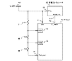
マイコンに具備されたADコンバータを利用する従来技術を図2を用いて説明する。
図2は従来のマイコンに具備されたADコンバータを利用した電源電圧検出回路を表す回路図である。
電圧検出回路は、電源(V_BAT)40を、マイコン50の電源端子(Vcc)11、定電圧レギュレータ20の電源端子(V_in)21にそれぞれ接続して電源供給を行っている。この電源40の電圧を検出するためには、抵抗(R1)34、抵抗(R3)35により電圧を分圧してADコンバータ端子(AD1)23に電圧を印加する。電源電圧検出のON、OFFはマイコン50の出力ポート(Port_out)14の出力設定により決定される。
A conventional technique using an AD converter included in a microcomputer will be described with reference to FIG.
FIG. 2 is a circuit diagram showing a power supply voltage detection circuit using an AD converter provided in a conventional microcomputer.
The voltage detection circuit supplies power by connecting the power supply (V_BAT) 40 to the power supply terminal (Vcc) 11 of the microcomputer 50 and the power supply terminal (V_in) 21 of the constant voltage regulator 20, respectively. In order to detect the voltage of the
電圧検出をONとする場合は、出力ポート14の出力レベルをLowレベルとする。電圧検出をONとした場合は、このとき出力ポート14の出力電圧が約0Vとなり、電源40(V_BAT)から抵抗(R1)34、抵抗(R3)35を介して一定の電流が流れ、既知の抵抗(R1)34、抵抗(R3)35により分圧された電圧がADコンバータ端子(AD1)23に入力される。
When turning on the voltage detection, the output level of the
定電圧レギュレータ20の出力(REG_out)22は、ADコンバータの基準電圧入力(V_refH)12に入力しているため、ADコンバータの読み値から電源電圧を計算できる。
電圧検出をOFFとする場合は、出力ポート(Port_out)14の出力レベルをHighレベルとする。このとき出力ポート(Port_out)14の出力電圧は、電源40(V_BAT)電圧と同一となるため、抵抗(R1)34、抵抗(R3)35には電流が流れず、低消費電流化を実現できる。
以上により、電圧検出回路は、電圧検出OFF時の低消費電流化を図りながら、電源電圧の検出を行っている。
Since the output (REG_out) 22 of the constant voltage regulator 20 is input to the reference voltage input (V_refH) 12 of the AD converter, the power supply voltage can be calculated from the reading value of the AD converter.
When turning off the voltage detection, the output level of the output port (Port_out) 14 is set to the High level. At this time, since the output voltage of the output port (Port_out) 14 becomes the same as the power supply 40 (V_BAT) voltage, no current flows through the resistor (R1) 34 and the resistor (R3) 35, and low current consumption can be realized. .
As described above, the voltage detection circuit detects the power supply voltage while reducing the current consumption when the voltage detection is OFF.
先行技術文献としては、例えば、特許文献1に、低電源電圧の検出レベルが低い場合でも、その低電源電圧を確実に検出して低電圧禁止を行わせることができるとともに、低電圧禁止時の消費電流を大幅に少なくする発明が開示されている。 As a prior art document, for example, in Patent Document 1, even when the detection level of a low power supply voltage is low, the low power supply voltage can be reliably detected and low voltage prohibition can be performed, and at the time of low voltage prohibition. An invention has been disclosed in which current consumption is significantly reduced.
従来の技術は、電源電圧の検出を行う際にマイコン50の出力ポート14のLowレベル電圧に起因する誤差が発生する。つまり、マイコン50毎にLowレベル電圧に誤差があるため、量産品の機器の場合、すべての機器で誤差なく正確に電源電圧を検出できないという課題がある。
本発明の目的は、マイコンの特性に起因する誤差なく正確に電源電圧を検出することである。
In the conventional technique, when the power supply voltage is detected, an error occurs due to the low level voltage of the
An object of the present invention is to accurately detect the power supply voltage without an error due to the characteristics of the microcomputer.
本発明の電圧検出回路は、少なくとも、2つのADコンバータと1つの出力ポートを有するマイコンと、3つの抵抗器を備え、前記3つの抵抗器は直列に接続され、電源に最も近い第1抵抗器は前記電源に接続された電圧線と第1ADコンバータとの間に接続され、第2抵抗器は前記第1ADコンバータと第2ADコンバータとの間に接続され、第3抵抗器は前記第2ADコンバータと前記出力ポートとの間に接続され、前記マイコンは、前記第1ADコンバータ及び前記第2ADコンバータから取得したデータと、前記第1抵抗器及び第2抵抗器の抵抗値から、前記電圧線の電圧を算出することを特徴とする。 The voltage detection circuit of the present invention includes at least a microcomputer having two AD converters and one output port, and three resistors, the three resistors being connected in series, and the first resistor closest to the power supply. Is connected between the voltage line connected to the power supply and the first AD converter, the second resistor is connected between the first AD converter and the second AD converter, and the third resistor is connected to the second AD converter. Connected between the output port and the microcomputer, the data obtained from the first AD converter and the second AD converter, and the resistance value of the first resistor and the second resistor, the voltage of the voltage line It is characterized by calculating.
なお、前記第1抵抗器の抵抗値をR1、前記第2抵抗器の抵抗値をR2、前記第1ADコンバータの電圧をV1、前記第2ADコンバータの電圧をV2とした場合、前記マイコンは、(R1/R2)×(V1−V2)+V1の計算式から前記電圧を算出することが好ましい。 When the resistance value of the first resistor is R1, the resistance value of the second resistor is R2, the voltage of the first AD converter is V1, and the voltage of the second AD converter is V2, the microcomputer It is preferable to calculate the voltage from the formula of (R1 / R2) * (V1-V2) + V1.
また、マイコンは、前記電圧線から電源供給を受けることが好ましい。 Further, it is preferable that the microcomputer be supplied with power from the voltage line.
さらに、定電圧レギュレータを有することが好ましい。 Further, it is preferable to have a constant voltage regulator.
本発明によれば、高精度な電源電圧の検出を行うことができる。 According to the present invention, it is possible to detect a power supply voltage with high accuracy.
以下、本発明の実施形態について図面を参照して詳細に説明する。
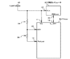
図1は本発明の一実施形態に係る電圧検出回路の回路図である。
図1において、電圧検出回路は、マイコン10と、定電圧レギュレータ20と、3つの抵抗器である抵抗(R1) 31、抵抗(R2) 32、抵抗(R3) 33で構成されている。
マイコン10は、少なくとも、2つのADコンバータ13、15と、1つの出力ポート14を内蔵している。
本発明の一実施形態に係る電圧検出回路は、従来の技術の図2に加えて抵抗(R2)32とADコンバータ(AD2)15が追加された構成となっている。
Hereinafter, embodiments of the present invention will be described in detail with reference to the drawings.
FIG. 1 is a circuit diagram of a voltage detection circuit according to an embodiment of the present invention.
In FIG. 1, the voltage detection circuit includes a microcomputer 10, a constant voltage regulator 20, and three resistors, a resistor (R1) 31, a resistor (R2) 32, and a resistor (R3) 33.
The microcomputer 10 contains at least two
The voltage detection circuit according to the embodiment of the present invention has a configuration in which a resistor (R2) 32 and an AD converter (AD2) 15 are added in addition to FIG.
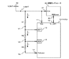
次に、本発明の電圧検出回路における詳細な動作について図3を用いて説明する。
図3は本発明の一実施形態に係る電圧検出回路の動作を説明するための図である。
図3は、各部の電圧、および電流、抵抗値を表した図である。
図3において、V1,V2,Vo,V_BATは各部の電圧を表し、Iは各部に流れる電流を表し、R1,R2,R3は各抵抗値を表している。なお、V1はADコンバータ13から得られる電圧値であり、V2はADコンバータ15から得られる電圧値である。
Next, detailed operation of the voltage detection circuit of the present invention will be described with reference to FIG.
FIG. 3 is a diagram for explaining the operation of the voltage detection circuit according to the embodiment of the present invention.
FIG. 3 is a diagram showing the voltage, current, and resistance value of each part.
In FIG. 3, V1, V2, Vo, V_BAT represent the voltage of each part, I represents the current flowing through each part, and R1, R2, R3 represent the respective resistance values. V1 is a voltage value obtained from the
図3において、電圧検出を行う際は、マイコン10の出力ポート(Port_out)14の出力をLowレベルに設定する。
この時、Voはマイコン10の出力ポート(Port_out)14のLowレベル電圧と一致する。しかし、マイコン10の出力ポート(Port_out)14のLowレベル電圧は、各マイコンの個別ばらつきにより一定値とならない。
In FIG. 3, when performing voltage detection, the output of the output port (Port_out) 14 of the microcomputer 10 is set to the Low level.
At this time, Vo matches the low level voltage of the output port (Port_out) 14 of the microcomputer 10. However, the low level voltage of the output port (Port_out) 14 of the microcomputer 10 does not become a constant value due to individual variation of each microcomputer.
図3におけるV_BAT,V1,V2は下式により算出できる。ただし、ADコンバータ端子は十分インピーダンスが高く、電流が流れないと仮定する。
V_BAT=I×(R1+R2+R3)+Vo ・・・ (式1)
V1=I×(R2+R3)+Vo ・・・ (式2)
V2=I×R3+Vo ・・・ (式3)
V_BAT, V1, and V2 in FIG. 3 can be calculated by the following formula. However, it is assumed that the AD converter terminal has sufficiently high impedance and no current flows.
V_BAT = I × (R1 + R2 + R3) + Vo (Equation 1)
V1 = I × (R2 + R3) + Vo (Equation 2)
V2 = I × R3 + Vo (Equation 3)
電流Iは、(式2)と(式3)から生成した(式4)で求まる。
I=(V1−V2)/R2 ・・・ (式4)
(式5)は(式1)と(式2)から求まる。
V_BAT=I×R1+V1 ・・・(式5)
The current I is obtained by (Equation 4) generated from (Equation 2) and (Equation 3).
I = (V1-V2) / R2 (Equation 4)
(Equation 5) is obtained from (Equation 1) and (Equation 2).
V_BAT = I × R1 + V1 (Equation 5)
さらに、(式6)は(式4)と(式5)から求まる。
V_BAT=(R1/R2)×(V1−V2)+V1 ・・・ (式6)
(式6)はVoによる誤差を含まないV_BATを算出できる。さらにR3が含まれなくなるため、抵抗の許容偏差の影響を低減することができる。
Furthermore, (Equation 6) is obtained from (Equation 4) and (Equation 5).
V_BAT = (R1 / R2) × (V1-V2) + V1 (Equation 6)
(Equation 6) can calculate V_BAT that does not include an error due to Vo. Furthermore, since R3 is not included, it is possible to reduce the influence of the allowable deviation of resistance.
(式7)は、従来の技術である図2でV_BATを求める式である。(式7)において、R1,R3は各抵抗値を表し、V1はADコンバータ23から得られる電圧値であり、Voはマイコン50の出力ポート(Port_out)14のLowレベル電圧であり、V_BATは電源(V_BAT)40の電圧である。
V_BAT=(R1/R3)× V1+Vo ・・・ (式7)
前記の通り、Voは各マイコンの個別のばらつきにより一定値とならず、最悪値で数百mVのオーダーとなる。この時、V_BATはVoで発生するLowレベル電圧がそのまま誤差として発生する。このため、従来の技術ではV_BATの偏差は最悪値で数百mVとなる。
(Equation 7) is an equation for obtaining V_BAT in FIG. 2 which is a conventional technique. In (Equation 7), R1 and R3 represent resistance values, V1 is a voltage value obtained from the
V_BAT = (R1 / R3) × V1 + Vo (Equation 7)
As described above, Vo does not have a constant value due to individual variation of each microcomputer, but has a worst value on the order of several hundred mV. At this time, as for V_BAT, the low level voltage generated at Vo is directly generated as an error. Therefore, in the conventional technique, the deviation of V_BAT is several hundred mV at the worst value.
一方、本発明による一実施形態に係る電圧検出回路は、(式6)より、抵抗の持つ許容偏差、およびV1,V2を測定する際のADコンバータの許容偏差のみとなる。
例えば、抵抗には許容偏差±0.5%の部品を使用し、AD変換器には12bitで絶対精度±8LSB品を使用し、定電圧レギュレータには±1%品を使用した場合、誤差は約1.7%となる。
本発明の電圧検出回路は、V_BATとして2.7Vを測定すると、V_BATの偏差は最大で46mVとなり、従来技術より高精度の電圧検出が可能となる。
On the other hand, the voltage detection circuit according to the embodiment of the present invention has only the allowable deviation of the resistor and the allowable deviation of the AD converter when measuring V1 and V2 from (Equation 6).
For example, if parts with a tolerance of ± 0.5% are used for resistors, 12-bit absolute accuracy is ± 8 LSB for the AD converter, and ± 1% for the constant voltage regulator, the error is about 1.7. %.
When the voltage detection circuit of the present invention measures 2.7 V as V_BAT, the maximum deviation of V_BAT is 46 mV, which makes it possible to detect voltage with higher accuracy than in the prior art.
本発明の実施形態である電圧検出回路は、高精度な電源電圧の検出を行うことができる。
ここで、本発明の実施形態には以下の発明が記載されている。つまり、少なくとも、2つのADコンバータと1つの出力ポートを有するマイコンと、3つの抵抗器を備え、前記3つの抵抗器は直列に接続され、電源に最も近い第1抵抗器は前記電源に接続された電圧線と第1ADコンバータとの間に接続され、第2抵抗器は前記第1ADコンバータと第2ADコンバータとの間に接続され、第3抵抗器は前記第2ADコンバータと前記出力ポートとの間に接続され、前記マイコンは、前記第1ADコンバータ及び前記第2ADコンバータから取得したデータと、前記第1抵抗器及び第2抵抗器の抵抗値から、前記電圧線の電圧を算出する電圧検出回路。
The voltage detection circuit according to the embodiment of the present invention can detect the power supply voltage with high accuracy.
Here, the following inventions are described in the embodiments of the present invention. That is, at least a microcomputer having two AD converters and one output port, and three resistors are provided, the three resistors are connected in series, and the first resistor closest to the power source is connected to the power source. Connected between the voltage line and the first AD converter, the second resistor is connected between the first AD converter and the second AD converter, and the third resistor is connected between the second AD converter and the output port. And a voltage detection circuit for calculating the voltage of the voltage line from the data obtained from the first AD converter and the second AD converter and the resistance values of the first resistor and the second resistor.
以上、本発明の一実施形態について詳細に説明したが、本発明は上述した実施形態に限定されるものではなく、本発明の趣旨を逸脱しない範囲で種々変更して実施することができる。 Although one embodiment of the present invention has been described in detail above, the present invention is not limited to the above-described embodiment, and various modifications can be made without departing from the spirit of the present invention.
マイコンに内蔵しているAD変換器のポートを2つ使用することによって、高精度な電源電圧の検出を行うことができるため、高精度な電源電圧の検出する用途に適用できる。 Since the power supply voltage can be detected with high accuracy by using two ports of the AD converter built in the microcomputer, it can be applied to the application for detecting the power supply voltage with high accuracy.
10,50:マイコン、20:定電圧レギュレータ、31:抵抗(R1)、32:抵抗(R2)、33:抵抗(R3)、34::抵抗(R1)、35:抵抗(R3)、40:電源(V_BAT)。 10, 50: Microcomputer, 20: Constant voltage regulator, 31: Resistor (R1), 32: Resistor (R2), 33: Resistor (R3), 34 :: Resistor (R1), 35: Resistor (R3), 40: Power supply (V_BAT).
Claims (2)
前記3つの抵抗器は直列に接続され、電源に最も近い第1抵抗器は前記電源に接続された電圧線と第1ADコンバータとの間に接続され、第2抵抗器は前記第1ADコンバータと第2ADコンバータとの間に接続され、第3抵抗器は前記第2ADコンバータと前記出力ポートとの間に接続され、
前記マイコンは、前記第1ADコンバータ及び前記第2ADコンバータから取得したデータと、前記第1抵抗器及び第2抵抗器の抵抗値から、前記電圧線の電圧を算出することを特徴とする電圧検出回路。 A voltage detection circuit including at least two AD converters, a microcomputer having one output port, and three resistors,
The three resistors are connected in series, the first resistor closest to the power supply is connected between the voltage line connected to the power supply and the first AD converter, and the second resistor is connected to the first AD converter and the first AD converter. A second resistor connected between the second AD converter and the second AD converter, and a third resistor connected between the second AD converter and the output port.
The microcomputer detects the voltage of the voltage line from the data acquired from the first AD converter and the second AD converter and the resistance values of the first resistor and the second resistor. .
前記第1抵抗器の抵抗値をR1、前記第2抵抗器の抵抗値をR2、前記第1ADコンバータの電圧をV1、前記第2ADコンバータの電圧をV2とした場合、
前記マイコンは、(R1/R2)×(V1−V2)+V1の計算式から前記電圧線の電圧を算出することを特徴とする電圧検出回路。 The voltage detection circuit according to claim 1, wherein
When the resistance value of the first resistor is R1, the resistance value of the second resistor is R2, the voltage of the first AD converter is V1, and the voltage of the second AD converter is V2,
The voltage detecting circuit, wherein the microcomputer calculates the voltage of the voltage line from a calculation formula of (R1 / R2) × (V1-V2) + V1.
Priority Applications (1)
| Application Number | Priority Date | Filing Date | Title |
|---|---|---|---|
| JP2016143328A JP6685196B2 (en) | 2016-07-21 | 2016-07-21 | Voltage detection circuit |
Applications Claiming Priority (1)
| Application Number | Priority Date | Filing Date | Title |
|---|---|---|---|
| JP2016143328A JP6685196B2 (en) | 2016-07-21 | 2016-07-21 | Voltage detection circuit |
Publications (2)
| Publication Number | Publication Date |
|---|---|
| JP2018013425A JP2018013425A (en) | 2018-01-25 |
| JP6685196B2 true JP6685196B2 (en) | 2020-04-22 |
Family
ID=61020608
Family Applications (1)
| Application Number | Title | Priority Date | Filing Date |
|---|---|---|---|
| JP2016143328A Active JP6685196B2 (en) | 2016-07-21 | 2016-07-21 | Voltage detection circuit |
Country Status (1)
| Country | Link |
|---|---|
| JP (1) | JP6685196B2 (en) |
Families Citing this family (1)
| Publication number | Priority date | Publication date | Assignee | Title |
|---|---|---|---|---|
| CN104698263A (en) * | 2013-12-09 | 2015-06-10 | 惠州市吉瑞科技有限公司 | System and method for detecting power supply voltages and power supply system |
Family Cites Families (10)
| Publication number | Priority date | Publication date | Assignee | Title |
|---|---|---|---|---|
| JPH10145208A (en) * | 1996-11-12 | 1998-05-29 | Hitachi Ltd | Electronic circuit device and voltage level detection circuit |
| JPH11339858A (en) * | 1998-05-28 | 1999-12-10 | Honda Motor Co Ltd | Battery state detection device and battery state detection unit |
| JP2000047307A (en) * | 1998-07-31 | 2000-02-18 | Olympus Optical Co Ltd | Battery driving equipment |
| JP2000131348A (en) * | 1998-10-28 | 2000-05-12 | New Japan Radio Co Ltd | Digital measuring device |
| JP4155978B2 (en) * | 2004-03-30 | 2008-09-24 | 三洋電機株式会社 | Power supply |
| JP5125289B2 (en) * | 2007-07-27 | 2013-01-23 | 株式会社ニコン | Power monitoring device, lens barrel and camera |
| JP4649489B2 (en) * | 2008-03-27 | 2011-03-09 | 株式会社日立製作所 | Total battery voltage detection circuit |
| JP5524729B2 (en) * | 2010-06-14 | 2014-06-18 | 本田技研工業株式会社 | Voltage detection circuit and power supply device |
| KR20130061814A (en) * | 2011-12-02 | 2013-06-12 | 삼성에스디아이 주식회사 | Circuit for measuring voltage of battery and power storage system using the same |
| JP2017096628A (en) * | 2014-03-28 | 2017-06-01 | 三洋電機株式会社 | Current detection device, power supply system |
-
2016
- 2016-07-21 JP JP2016143328A patent/JP6685196B2/en active Active
Also Published As
| Publication number | Publication date |
|---|---|
| JP2018013425A (en) | 2018-01-25 |
Similar Documents
| Publication | Publication Date | Title |
|---|---|---|
| TWI588641B (en) | Constant voltage circuit | |
| TWI720285B (en) | Voltage generating apparatus and calibration method thereof | |
| CN105659326B (en) | Current sensing circuit with offset calibration | |
| CN108693916B (en) | Overcurrent protection circuit and voltage regulator | |
| CN103455078B (en) | A kind of current-limiting circuit, device | |
| US20180006018A1 (en) | Power converter and semiconductor device | |
| CN105223411A (en) | Overcurrent detection circuit and power supply system | |
| CN101128742A (en) | Current measuring device, testing device, current measuring method, and testing method | |
| JP6685196B2 (en) | Voltage detection circuit | |
| CN107228967B (en) | Current detection circuit | |
| US20220350360A1 (en) | Piecewise Correction of Errors Over Temperature without Using On-Chip Temperature Sensor/Comparators | |
| US7928711B2 (en) | Linear voltage regulator with accurate open load detection | |
| CN115902369A (en) | Current sensor | |
| JP5729254B2 (en) | Hysteresis device | |
| CN110114638B (en) | Analog input unit and reference voltage stabilization circuit | |
| CN111367346A (en) | Voltage stabilizing circuit, power supply and electric equipment | |
| CN109564139B (en) | Sensor device | |
| CN115932377B (en) | Current sensor | |
| CN105548651B (en) | Measuring device | |
| JP4768704B2 (en) | Current detection circuit | |
| CN104682466A (en) | Calibration method and calibration circuit for charging control circuit | |
| JP6386970B2 (en) | Sensor abnormality detection device and sensor device | |
| JP2016090379A (en) | measuring device | |
| US20240097632A1 (en) | Integrated circuit and semiconductor device | |
| JP4301184B2 (en) | Linear regulator output voltage measuring apparatus and linear regulator output voltage measuring method |
Legal Events
| Date | Code | Title | Description |
|---|---|---|---|
| A621 | Written request for application examination |
Free format text: JAPANESE INTERMEDIATE CODE: A621 Effective date: 20190327 |
|
| A977 | Report on retrieval |
Free format text: JAPANESE INTERMEDIATE CODE: A971007 Effective date: 20200221 |
|
| A131 | Notification of reasons for refusal |
Free format text: JAPANESE INTERMEDIATE CODE: A131 Effective date: 20200227 |
|
| A521 | Request for written amendment filed |
Free format text: JAPANESE INTERMEDIATE CODE: A523 Effective date: 20200303 |
|
| TRDD | Decision of grant or rejection written | ||
| A01 | Written decision to grant a patent or to grant a registration (utility model) |
Free format text: JAPANESE INTERMEDIATE CODE: A01 Effective date: 20200319 |
|
| A61 | First payment of annual fees (during grant procedure) |
Free format text: JAPANESE INTERMEDIATE CODE: A61 Effective date: 20200331 |
|
| R150 | Certificate of patent or registration of utility model |
Ref document number: 6685196 Country of ref document: JP Free format text: JAPANESE INTERMEDIATE CODE: R150 |
|
| R250 | Receipt of annual fees |
Free format text: JAPANESE INTERMEDIATE CODE: R250 |
|
| R250 | Receipt of annual fees |
Free format text: JAPANESE INTERMEDIATE CODE: R250 |
|
| S533 | Written request for registration of change of name |
Free format text: JAPANESE INTERMEDIATE CODE: R313533 |
|
| R350 | Written notification of registration of transfer |
Free format text: JAPANESE INTERMEDIATE CODE: R350 |
|
| R250 | Receipt of annual fees |
Free format text: JAPANESE INTERMEDIATE CODE: R250 |