JP6680552B2 - Shape measuring device and method of manufacturing object to be coated - Google Patents
Shape measuring device and method of manufacturing object to be coated Download PDFInfo
- Publication number
- JP6680552B2 JP6680552B2 JP2016021831A JP2016021831A JP6680552B2 JP 6680552 B2 JP6680552 B2 JP 6680552B2 JP 2016021831 A JP2016021831 A JP 2016021831A JP 2016021831 A JP2016021831 A JP 2016021831A JP 6680552 B2 JP6680552 B2 JP 6680552B2
- Authority
- JP
- Japan
- Prior art keywords
- value
- light
- brightness
- objective lens
- images
- Prior art date
- Legal status (The legal status is an assumption and is not a legal conclusion. Google has not performed a legal analysis and makes no representation as to the accuracy of the status listed.)
- Expired - Fee Related
Links
Images


Classifications
-
- G—PHYSICS
- G01—MEASURING; TESTING
- G01B—MEASURING LENGTH, THICKNESS OR SIMILAR LINEAR DIMENSIONS; MEASURING ANGLES; MEASURING AREAS; MEASURING IRREGULARITIES OF SURFACES OR CONTOURS
- G01B11/00—Measuring arrangements characterised by the use of optical techniques
- G01B11/24—Measuring arrangements characterised by the use of optical techniques for measuring contours or curvatures
- G01B11/2441—Measuring arrangements characterised by the use of optical techniques for measuring contours or curvatures using interferometry
-
- G—PHYSICS
- G01—MEASURING; TESTING
- G01B—MEASURING LENGTH, THICKNESS OR SIMILAR LINEAR DIMENSIONS; MEASURING ANGLES; MEASURING AREAS; MEASURING IRREGULARITIES OF SURFACES OR CONTOURS
- G01B9/00—Measuring instruments characterised by the use of optical techniques
- G01B9/02—Interferometers
- G01B9/02015—Interferometers characterised by the beam path configuration
- G01B9/02029—Combination with non-interferometric systems, i.e. for measuring the object
- G01B9/0203—With imaging systems
-
- G—PHYSICS
- G01—MEASURING; TESTING
- G01B—MEASURING LENGTH, THICKNESS OR SIMILAR LINEAR DIMENSIONS; MEASURING ANGLES; MEASURING AREAS; MEASURING IRREGULARITIES OF SURFACES OR CONTOURS
- G01B9/00—Measuring instruments characterised by the use of optical techniques
- G01B9/02—Interferometers
- G01B9/0209—Low-coherence interferometers
-
- G—PHYSICS
- G02—OPTICS
- G02B—OPTICAL ELEMENTS, SYSTEMS OR APPARATUS
- G02B27/00—Optical systems or apparatus not provided for by any of the groups G02B1/00 - G02B26/00, G02B30/00
- G02B27/10—Beam splitting or combining systems
- G02B27/12—Beam splitting or combining systems operating by refraction only
- G02B27/123—The splitting element being a lens or a system of lenses, including arrays and surfaces with refractive power
-
- G—PHYSICS
- G02—OPTICS
- G02B—OPTICAL ELEMENTS, SYSTEMS OR APPARATUS
- G02B7/00—Mountings, adjusting means, or light-tight connections, for optical elements
- G02B7/28—Systems for automatic generation of focusing signals
- G02B7/36—Systems for automatic generation of focusing signals using image sharpness techniques, e.g. image processing techniques for generating autofocus signals
- G02B7/38—Systems for automatic generation of focusing signals using image sharpness techniques, e.g. image processing techniques for generating autofocus signals measured at different points on the optical axis, e.g. focussing on two or more planes and comparing image data
-
- G—PHYSICS
- G06—COMPUTING OR CALCULATING; COUNTING
- G06T—IMAGE DATA PROCESSING OR GENERATION, IN GENERAL
- G06T7/00—Image analysis
- G06T7/50—Depth or shape recovery
- G06T7/55—Depth or shape recovery from multiple images
- G06T7/571—Depth or shape recovery from multiple images from focus
-
- G—PHYSICS
- G06—COMPUTING OR CALCULATING; COUNTING
- G06T—IMAGE DATA PROCESSING OR GENERATION, IN GENERAL
- G06T7/00—Image analysis
- G06T7/70—Determining position or orientation of objects or cameras
- G06T7/73—Determining position or orientation of objects or cameras using feature-based methods
-
- G—PHYSICS
- G01—MEASURING; TESTING
- G01B—MEASURING LENGTH, THICKNESS OR SIMILAR LINEAR DIMENSIONS; MEASURING ANGLES; MEASURING AREAS; MEASURING IRREGULARITIES OF SURFACES OR CONTOURS
- G01B11/00—Measuring arrangements characterised by the use of optical techniques
- G01B11/02—Measuring arrangements characterised by the use of optical techniques for measuring length, width or thickness
- G01B11/026—Measuring arrangements characterised by the use of optical techniques for measuring length, width or thickness by measuring distance between sensor and object
-
- G—PHYSICS
- G06—COMPUTING OR CALCULATING; COUNTING
- G06T—IMAGE DATA PROCESSING OR GENERATION, IN GENERAL
- G06T2207/00—Indexing scheme for image analysis or image enhancement
- G06T2207/10—Image acquisition modality
- G06T2207/10056—Microscopic image
- G06T2207/10061—Microscopic image from scanning electron microscope
-
- G—PHYSICS
- G06—COMPUTING OR CALCULATING; COUNTING
- G06T—IMAGE DATA PROCESSING OR GENERATION, IN GENERAL
- G06T2207/00—Indexing scheme for image analysis or image enhancement
- G06T2207/30—Subject of image; Context of image processing
- G06T2207/30108—Industrial image inspection
- G06T2207/30148—Semiconductor; IC; Wafer
-
- G—PHYSICS
- G06—COMPUTING OR CALCULATING; COUNTING
- G06T—IMAGE DATA PROCESSING OR GENERATION, IN GENERAL
- G06T7/00—Image analysis
- G06T7/10—Segmentation; Edge detection
- G06T7/13—Edge detection
Landscapes
- Physics & Mathematics (AREA)
- General Physics & Mathematics (AREA)
- Engineering & Computer Science (AREA)
- Computer Vision & Pattern Recognition (AREA)
- Optics & Photonics (AREA)
- Theoretical Computer Science (AREA)
- Length Measuring Devices By Optical Means (AREA)
Description
この発明は形状測定装置および当該形状測定装置を用いた被塗布対象物の製造方法に関する。より特定的には、この発明は、金属、樹脂、およびそれらの加工品の表面形状を測定する形状測定装置、あるいは半導体基板、プリント基板、およびフラットパネルディスプレイなどの基板の表面の形状を測定するための形状測定装置、および当該形状測定装置を用いた被塗布対象物の製造方法に関する。 The present invention relates to a shape measuring apparatus and a method for manufacturing an object to be coated using the shape measuring apparatus. More specifically, the present invention measures the shape of a surface of a substrate such as a semiconductor substrate, a printed circuit board, and a flat panel display, or a shape measuring device for measuring the surface shape of a metal, a resin, and a processed product thereof. And a method for manufacturing an object to be coated using the shape measuring apparatus.
特開2015−7564(特許文献1)には、基板の表面に塗布されたインクからなるインク塗布部の上方に二光束干渉対物レンズを位置決めした後、Zステージを移動させながら干渉光の画像を取得し、当該画像を構成する複数の画素の各々についてコントラスト値がピークとなるZステージの位置を当該画素の合焦位置として、インク塗布部の高さを求める塗布装置が開示されている。 In JP-A-2015-7564 (Patent Document 1), after the two-beam interference objective lens is positioned above the ink application part made of ink applied to the surface of the substrate, the image of the interference light is displayed while moving the Z stage. There is disclosed an application device that obtains the height of an ink application unit by using the position of the Z stage at which the contrast value reaches a peak for each of a plurality of pixels forming the image, as the focus position of the pixel.
二光束干渉対物レンズは、対象物表面の反射光と参照光を干渉させることにより干渉光を得る。たとえば対象物が平面で、対象物が対物レンズの光軸に対して垂直に配置される場合、反射光は正反射光となり、干渉光のコントラストは大きい。しかしながら、対象物が傾斜した状態では、対物レンズの開口に戻る反射光が減少し、反射光の強度が低下する。これにより、干渉光のコントラストも低下する。 The two-beam interference objective lens obtains interference light by causing the reflected light on the surface of the object and the reference light to interfere with each other. For example, when the object is a plane and the object is arranged perpendicular to the optical axis of the objective lens, the reflected light becomes specularly reflected light, and the contrast of the interference light is large. However, when the object is tilted, the reflected light returning to the aperture of the objective lens is reduced and the intensity of the reflected light is reduced. This also reduces the contrast of the interference light.
干渉光のコントラストが低下すると、対象物と対物レンズとの距離を変化させた場合に、コントラストの明確なピークが生じにくくなり、ピークの検出が困難となる。ピークを検出できない場所の高さは不定となり、対象物の形状を正確に測定することは困難になる。 When the contrast of the interference light is reduced, when the distance between the object and the objective lens is changed, a clear contrast peak is less likely to occur, and it becomes difficult to detect the peak. The height of the place where the peak cannot be detected becomes indefinite, and it becomes difficult to accurately measure the shape of the object.
この発明の主たる目的は、対象物の形状を正確に測定することができる形状測定装置を提供することである。 A main object of the present invention is to provide a shape measuring device capable of accurately measuring the shape of an object.
この発明に係る形状測定装置は、対象物に白色光を照射して、対象物からの反射光を用いて対象物の形状を測定する。形状測定装置は、光源と、二光束干渉対物レンズと、撮像装置と、観察光学系と、位置決め装置と、制御装置とを備える。光源は、白色光を出力する。二光束干渉対物レンズは、光源から出力された白色光を二光束に分離し、一方の光束を対象物に照射するとともに他方の光束を参照面に照射し、対象物からの反射光と参照面からの反射光とを干渉させて干渉光を出力するように構成される。撮像装置は、二光束干渉対物レンズから出力される干渉光の画像を取得するように構成される。観察光学系は、光源から出力された白色光を、二光束干渉対物レンズを介して対象物の表面に導き、表面からの反射光を二光束干渉対物レンズを介して撮像装置に導く。位置決め装置は、二光束干渉対物レンズを対象物に対して相対的に移動させるように構成される。制御装置は、対象物と二光束干渉対物レンズとの距離を二光束干渉対物レンズの光軸方向に変化させながら複数の画像を取得し、複数の画像を用いて対象物の形状を測定するように構成される。制御装置は、複数の画像における各単位領域について、複数の画像にわたって輝度に基づく評価値が最大となる二光束干渉対物レンズの位置を当該単位領域の合焦位置として算出し、複数の画像における各単位領域の合焦位置に基づいて対象物の形状を測定するように構成される。制御装置は、評価値として、複数の画像における各単位領域の輝度、および当該単位領域の輝度と当該単位領域に近接する複数の単位領域の輝度との差に相関関係のある値を用いるように構成される。 A shape measuring device according to the present invention irradiates an object with white light and measures the shape of the object using reflected light from the object. The shape measuring device includes a light source, a two-beam interference objective lens, an imaging device, an observation optical system, a positioning device, and a control device. The light source outputs white light. The two-beam interference objective lens separates the white light output from the light source into two light beams, irradiates one of the light beams to the object and the other light beam to the reference surface, and the reflected light from the object and the reference surface. It is configured to interfere with the reflected light from and output the interference light. The imaging device is configured to acquire an image of the interference light output from the two-beam interference objective lens. The observation optical system guides the white light output from the light source to the surface of the object through the two-beam interference objective lens, and guides the reflected light from the surface to the imaging device through the two-beam interference objective lens. The positioning device is configured to move the two-beam interference objective lens relative to the object. The controller acquires a plurality of images while changing the distance between the object and the two-beam interference objective lens in the optical axis direction of the two-beam interference objective lens, and measures the shape of the object using the plurality of images. Is composed of. The control device calculates, for each unit area in the plurality of images, the position of the two-beam interference objective lens having the maximum evaluation value based on the luminance over the plurality of images as the focus position of the unit area, and in each of the plurality of images. It is configured to measure the shape of the object based on the focus position of the unit area. The control device uses, as the evaluation value, a value having a correlation with the brightness of each unit area in the plurality of images, and the difference between the brightness of the unit area and the brightness of the plurality of unit areas adjacent to the unit area. Composed.
この発明に係る形状測定装置によれば、評価値として、複数の画像における各単位領域の輝度に加えて、当該単位領域の輝度と当該単位領域に近接する複数の単位領域の輝度との差に相関関係のある値を用いることにより、各単位領域の合焦位置を精度よく算出することができる。その結果、対象物の形状を正確に測定することができる。 According to the shape measuring device of the present invention, as the evaluation value, in addition to the brightness of each unit area in the plurality of images, the difference between the brightness of the unit area and the brightness of the plurality of unit areas close to the unit area is evaluated. By using the values having the correlation, the in-focus position of each unit area can be accurately calculated. As a result, the shape of the object can be accurately measured.
[形状測定装置の構成]
図1は、この発明の一実施の形態による形状測定装置1の構成を示す図である。図1において、この形状測定装置1は、光源2、光源制御器3、二光束干渉対物レンズ4、観察光学系5、撮像装置6、Zステージ7、Zステージ制御器8、支持部材9、ベース板10、制御装置11、キーボード12、マウス13、およびモニタ14を備える。観察光学系5は、支持部材9を介してベース板10に取り付けられる。平板状の被測定部品15は、ベース板10の表面に置かれる。形状測定装置1は、被測定部品15表面の形状を測定する。
[Configuration of shape measuring device]
FIG. 1 is a diagram showing a configuration of a
光源2は、観察光学系5の側面に設けられ、白色光を出射する。光源制御器3は、光源2に接続され、制御装置11からの指示に従って白色光の明るさを制御する。光源制御器3は、たとえば光源2に供給される電力を制御することにより、白色光の明るさを制御することができる。光源2から出射された白色光は、観察光学系5を介して二光束干渉対物レンズ4に入射される。被測定部品15に照射される光が白色光である場合、レーザなどの単一波長の光と異なり、撮像装置6で取得される干渉光の画像における輝度は、一般的に二光束干渉対物レンズ4の合焦位置で最大になる。そのため、合焦位置に基づいて被測定部品15の形状を測定するには、白色光が適している。
The
二光束干渉対物レンズ4は、Zステージ7を介して観察光学系5の下端に設けられる。二光束干渉対物レンズ4は、光源2からの白色光を二光束に分離する。二光束干渉対物レンズ4は、一方の光束を被測定部品15の表面に照射するとともに他方の光束を参照面に照射する。二光束干渉対物レンズ4は、被測定部品15の表面からの反射光と参照面からの反射光とを干渉させて干渉光を生成する。実施の形態では、二光束干渉対物レンズ4としてミラウ型干渉対物レンズを用いる場合について説明する。二光束干渉対物レンズ4は、マイケルソン型やリニーク型の干渉対物レンズを用いてもよい。
The two-beam interference
観察光学系5は、二光束干渉対物レンズ4によって生成された干渉光を観察するために設けられている。
The observation
撮像装置6は、制御装置11によって制御され、観察光学系5を介して干渉光の画像を一定周期で取得する。撮像装置6は、取得した画像を制御装置11に出力する。
The
Zステージ7は、観察光学系5の下端に設けられ、二光束干渉対物レンズ4をその光軸方向に移動させる。
The Z stage 7 is provided at the lower end of the observation
Zステージ制御器8は、制御装置11からの指示に従ってZステージ7を二光束干渉対物レンズ4の光軸方向に移動させる。
The
Zステージ7によって二光束干渉対物レンズ4を移動させる代わりに、被測定部品15をテーブルで上下させてもよい。あるいは、二光束干渉対物レンズ4と観察光学系5の連結部にテーブルなどを取り付けて二光束干渉対物レンズ4の光軸方向の位置を調整してもよい。あるいは、これらのテーブルとして、位置決めを圧電素子で行うピエゾテーブルを用いてもよい。
Instead of moving the two-beam interference
制御装置11は、たとえばパーソナルコンピュータによって構成されている。制御装置11には、キーボード12、マウス13、およびモニタ14が接続されている。形状測定装置1の使用者は、キーボード12およびマウス13を用いて、形状測定の開始、終了などを制御装置11に指令し、測定された被測定部品15の形状をモニタ14で確認する。制御装置11は、キーボード12、マウス13などからの信号に従って、形状測定装置1全体を制御し、被測定部品15の形状を測定する。
The
[制御装置の構成]
図2は、図1に示した制御装置11の機能を説明するための機能ブロック図である。図2に示されるように、制御装置11は、演算処理部41、画像入力部42、データ記憶部43、位置制御値出力部44、および照明制御値出力部45を含む。
[Configuration of control device]
FIG. 2 is a functional block diagram for explaining the functions of the
演算処理部41は、キーボード12、マウス13などを用いて与えられた情報に基づいて、Zステージ7の高さに応じた電圧値に対応する値を格納する位置指令値配列、およびZステージ7の高さに応じた光源2の明るさに対応する値を格納する照明指令値配列を生成する。位置指令値配列は、Zステージ7の位置(被測定部品15からの高さ)を制御するために用いられる。照明指令値配列は、Zステージ7の位置に応じて光源2の明るさを制御するために用いられる。演算処理部41は、位置指令値配列および照明指令値配列をデータ記憶部43に書き込む。実施の形態においては、光源2の明るさをほぼ一定に保つため、照明指令値配列の値は一定である。
The
位置制御値出力部44は、データ記憶部43から位置指令値配列を読み出す。位置制御値出力部44は、位置指令値配列に従って制御電圧EZを出力する。
The position control
Zステージ制御器8は、位置制御値出力部44から出力される制御電圧EZに応じた位置にZステージ7を移動させる。
The
照明制御値出力部45は、データ記憶部43から照明指令値配列を読み出す。照明制御値出力部45は、照明指令値配列に従って制御電圧ELを出力する。実施の形態においては、照明指令値配列はほぼ一定であるため、制御電圧ELはほぼ一定である。
The illumination control
光源制御器3は、照明制御値出力部45から出力される制御電圧ELに応じて、光源2の明るさを変化させることができる。
The
画像入力部42は、位置制御値出力部44によるデータ記憶部43からの位置指令値配列の読込みに同期して動作する。画像入力部42は、撮像装置6によって撮影された画像を一定周期で取得する。画像入力部42は、取得した画像をデータ記憶部43に格納する。
The
[合焦位置検出の原理]
図3は、図1に示した二光束干渉対物レンズ4の構成を示す図である。図3に示されるように、二光束干渉対物レンズ4は、レンズ21、参照鏡22、およびビームスプリッタ23を含む。参照鏡22は、レンズ21の、被測定部品15を向いている側の中央部に設けられている。ビームスプリッタ23は、レンズ21と被測定部品15との間に設けられている。
[Principle of in-focus position detection]
FIG. 3 is a diagram showing the configuration of the two-beam interference
レンズ21に入射した光は、ビームスプリッタ23によって被測定部品15の方向に通過する光と参照鏡22の方向に反射する2つの光に分けられる。被測定部品15の表面で反射した光L1と参照鏡22の表面で反射した光L2は再びビームスプリッタ23で合流し、レンズ21によって集光される。
The light that has entered the
図4は、図1に示した観察光学系5の構成を示す図である。図4に示されるように、観察光学系5は、集光レンズ31、ハーフミラー32、および結像レンズ33を含む。二光束干渉対物レンズ4の光軸と、結像レンズ33の光軸とはほぼ一致しており、ともに撮像装置6の撮像面6Aの中心を通過している。光源2の光軸と集光レンズ31の光軸とはほぼ一致しており、ともに二光束干渉対物レンズ4の光軸とほぼ直交している。光源2と集光レンズ31との間には、不要な波長の光を除去するためのフィルタ34が設けられている。ハーフミラー32は、光源2の光軸と二光束干渉対物レンズ4の光軸との交点に設けられている。ハーフミラー32は、光源2の光軸および二光束干渉対物レンズ4の光軸の各々に対してほぼ45度の角度で配置されている。
FIG. 4 is a diagram showing the configuration of the observation
光源2から出射されてフィルタ34を通過した光は、ハーフミラー32によってレンズ21の方向に反射される。レンズ21に入射した光は、ビームスプリッタ23によって被測定部品15の方向に通過する光と参照鏡22の方向に反射する2つの光に分けられる。被測定部品15および参照鏡22の表面で反射した光は再びビームスプリッタ23で合流し、レンズ21によって集光される。レンズ21から出た光は、ハーフミラー32を通過して、結像レンズ33を経て撮像装置6の撮像面6Aに入射する。
The light emitted from the
撮像面6Aにおいて、被測定部品15の表面で反射した光L1と参照鏡22の表面で反射した光L2との干渉光の画像が取得される。干渉光の強度は、光L1の光路長および光L2の光路長の差に応じて変化する。
On the imaging surface 6A, an image of the interference light of the light L1 reflected on the surface of the
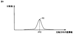
図5は、二光束干渉対物レンズ4を光軸方向に移動させた場合の干渉光の強度の変化を示す図である。図5の横軸は、光軸方向の座標(Zステージ7の位置)を示す。図5の縦軸は、撮像面6Aにおいて取得される画像における干渉光の強度を示している。
FIG. 5 is a diagram showing changes in the intensity of the interference light when the two-beam interference
二光束干渉対物レンズ4は、対象物表面の反射光と参照光を干渉させることにより干渉光を得る。干渉光の強度は、図5に示されるようにZステージ7の位置に応じて、ある値を中心にして一定周期で振動し、その振幅はコントラストに相当する。また、振幅が最大となるP1はレンズ21の合焦位置である。ここで、たとえば被測定部品15が平面で、被測定部品15が対物レンズの光軸に対して垂直に配置された場合、反射光は正反射光となり、干渉光のコントラストは大きい。しかしながら、被測定部品15が傾斜した状態では、対物レンズ21の開口に戻る光L1が減少し、反射光の強度が低下する。これにより、干渉光のコントラストも低下する。
The two-beam interference
干渉光のコントラストが低下すると、対象物と対物レンズとの距離を変化させた場合に、コントラストの明確なピークが生じにくくなり、ピークP1の検出が困難となる。ピークを検出できない場所の高さは不定となり、対象物の形状を正確に測定することは困難になる。 When the contrast of the interference light is lowered, when the distance between the object and the objective lens is changed, a clear contrast peak is less likely to occur, and it becomes difficult to detect the peak P1. The height of the place where the peak cannot be detected becomes indefinite, and it becomes difficult to accurately measure the shape of the object.
しかしながら、被測定部品15の表面の凹凸による反射光量の違いは、撮像装置6で取得される画像における画素間の明暗の差として確認することができる場合がある。
However, the difference in the amount of reflected light due to the unevenness of the surface of the
そこで実施の形態では、合焦位置を求めるために必要な評価値として、合焦位置を算出する対象である注目画素の輝度に加えて、注目画素の輝度と注目画素に近接する複数の単位領域の輝度との差に相関関係のある評価値として、注目画素の輝度と注目画素に近接する近接領域に含まれる画素の輝度との分散値を用いて、各画素の合焦位置を算出する。 Therefore, in the embodiment, as the evaluation value necessary for obtaining the focus position, in addition to the brightness of the target pixel whose focus position is to be calculated, the brightness of the target pixel and a plurality of unit areas close to the target pixel As the evaluation value having a correlation with the brightness of the target pixel, the focus position of each pixel is calculated by using the variance value of the brightness of the target pixel and the brightness of the pixel included in the proximity area close to the target pixel.
図6は、二光束干渉対物レンズ4を光軸方向に移動させた場合の干渉光の強度の分散値の変化を示す図である。図6の横軸は、光軸方向の座標(Zステージ7の位置)を示す。図6の縦軸は、干渉光の強度の分散値を示している。図6に示されるように、被測定部品15と二光束干渉対物レンズ4との距離を変化させた場合に、分散値に関して明確なピークP2が生じている。ピークP2に対応する位置FP2は、合焦位置にほぼ一致する。そのため、分散値を用いることにより注目画素の合焦位置を精度よく算出することができる。その結果、被測定部品15の形状を正確に測定することができる。
FIG. 6 is a diagram showing a change in the dispersion value of the intensity of the interference light when the two-beam interference
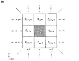
図7は、撮像装置6によって取得される画像を構成する複数の画素を模式的に示す図である。撮像装置6によって取得される画像を構成する各画素は、位置(x,y)によって特定される。画素の座標値xは、0からMxまでのいずれかの値をとる。画素の座標値yは、0からMyまでのいずれかの値をとる。実施の形態において、画像上の位置が(x,y)である画素Cxyにおける分散値V(x,y)は、画素Cxyを中心とするA×Bの近接領域RABに含まれる画素の輝度G(i,j)を用いて、以下の式(1)で表される。
FIG. 7 is a diagram schematically showing a plurality of pixels forming an image acquired by the

式(1)においては、Gaveは近接領域RABの輝度の平均値であり、以下の式(2)で表される。 In Expression (1), G ave is the average value of the brightness of the proximity area R AB and is expressed by Expression (2) below.
輝度に関する分散値以外に、注目画素を含む近接領域を構成する複数の画素の各々の輝度と注目画素の輝度との差に相関関係があり、合焦位置でピークを示す評価値として、たとえば、画像のエッジ検出に用いられる輝度に関する一次微分値、あるいは二次微分値を挙げることができる。輝度に関する一次微分値としては、以下の式(3)で表されるグラディエントD1aを挙げることができる。 In addition to the variance value related to the brightness, there is a correlation in the difference between the brightness of each of the plurality of pixels forming the proximity region including the target pixel and the brightness of the target pixel, and as an evaluation value indicating a peak at the focus position, for example, A primary differential value or a secondary differential value relating to luminance used for edge detection of an image can be mentioned. As the first-order differential value relating to luminance, a gradient D1a represented by the following formula (3) can be given.
D1a(x,y)=|G(x+1,y−1)−G(x−1,y−1)|+|G(x+1,y)−G(x−1,y)|+|G(x+1,y+1)−G(x−1,y+1)|+|G(x−1,y+1)−G(x−1,y−1)|+|G(x,y+1)−G(x,y−1)|+|G(x+1,y+1)−G(x+1,y−1)| …(3)
グラディエントD1aは、注目画素に隣接する画素のうち、画素の位置を規定する座標軸のx軸方向に向き合う画素間の輝度の傾きの絶対値、およびy軸方向に向き合う画素間の輝度の傾きの絶対値の和である。なお、画素間の輝度の傾きとは、画素間の輝度の差である。
D1a (x, y) = | G (x + 1, y-1) -G (x-1, y-1) | + | G (x + 1, y) -G (x-1, y) | + | G ( x + 1, y + 1) -G (x-1, y + 1) | + | G (x-1, y + 1) -G (x-1, y-1) | + | G (x, y + 1) -G (x, y) -1) | + | G (x + 1, y + 1) -G (x + 1, y-1) | ... (3)
The gradient D1a is the absolute value of the brightness gradient between pixels facing in the x-axis direction of the coordinate axes that define the pixel position among the pixels adjacent to the pixel of interest, and the absolute brightness gradient between pixels facing in the y-axis direction. It is the sum of the values. The inclination of the luminance between pixels is the difference in luminance between pixels.
図8は、注目画素Cxyに隣接する画素を示す図である。図8に示されるように、注目画素Cxyは、画素Cx−1,y,Cx,y+1,Cx+1,y+1,Cx+1,y,Cx+1,y−1,Cx,y−1,Cx−1,y−1,Cx−1,yに囲まれている。図8および式(3)を参照しながら、グラディエントD1aは、x軸方向に向き合う画素Cx+1,y−1およびCx−1,y−1の間の輝度の傾きの絶対値(|G(x+1,y−1)−G(x−1,y−1)|)、画素Cx+1,yおよびCx−1,yの間の輝度の傾きの絶対値(|G(x+1,y)−G(x−1,y)|)、画素Cx+1,y+1およびCx−1,y+1の間の輝度の傾きの絶対値(|G(x+1,y+1)−G(x−1,y+1)|)、y軸方向に向き合う画素Cx−1,y+1およびCx−1,y−1の間の輝度の傾きの絶対値(|G(x−1,y+1)−G(x−1,y−1)|)、画素Cx,y+1およびCx,y−1の間の輝度の傾きの絶対値(|G(x,y+1)−G(x,y−1)|)、並びに画素Cx+1,y+1およびCx+1,y−1の間の輝度の傾きの絶対値(|G(x+1,y+1)−G(x+1,y−1)|)の和である。 FIG. 8 is a diagram showing pixels adjacent to the target pixel C xy . As shown in FIG. 8, the pixel of interest C xy is the pixel C x-1, y , C x, y + 1 , C x + 1, y + 1 , C x + 1, y , C x + 1, y-1 , C x, y-1. , C x−1, y−1 , C x−1, y . With reference to FIG. 8 and Expression (3), the gradient D1 a is the absolute value (| G) of the slope of the luminance between the pixels C x + 1, y−1 and C x−1, y−1 facing in the x-axis direction. (X + 1, y−1) −G (x−1, y−1) |), the absolute value of the slope of the luminance between the pixels C x + 1, y and C x−1, y (| G (x + 1, y). -G (x-1, y) |), the absolute value of the slope of the luminance between the pixels Cx + 1, y + 1 and Cx-1, y + 1 (| G (x + 1, y + 1) -G (x-1, y + 1). |), The absolute value of the slope of the luminance between the pixels Cx-1, y + 1 and Cx-1, y-1 facing in the y-axis direction (| G (x-1, y + 1) -G (x-1, y-1) |), the pixel C x, y + 1 and C x, the absolute value of the luminance gradient between y-1 (| G (x , y + 1) -G (x, y-1) |), and The sum of the unit C x + 1, y + 1 and C x + 1, the luminance magnitude of the slope of between y-1 (| | G ( x + 1, y + 1) -G (x + 1, y-1)).
輝度に関する一次微分値としては、以下の式(4)で表されるグラディエントD1bを用いることもできる。 The gradient D1b represented by the following equation (4) can also be used as the first-order differential value relating to the luminance.
D1b(x,y)=D1a(x,y)+|G(x+1,y+1)−G(x−1,y−1)|+|G(x+1,y−1)−G(x−1,y+1)| …(4)
グラディエントD1bは、注目画素に隣接する画素のうち、画素の位置を規定する座標軸の対角線方向に向き合う画素間の輝度の傾きの絶対値を、グラディエントD1aに加えたものである。
D1b (x, y) = D1a (x, y) + | G (x + 1, y + 1) -G (x-1, y-1) | + | G (x + 1, y-1) -G (x-1, y + 1) | ... (4)
The gradient D1b is obtained by adding, to the gradient D1a, the absolute value of the inclination of the luminance between the pixels, which are adjacent to the pixel of interest and face each other in the diagonal direction of the coordinate axis that defines the position of the pixel.
図8および式(4)を参照しながら、グラディエントD1bは、グラディエントD1a、対角線方向に向き合う画素Cx+1,y+1およびCx−1,y−1の間の輝度の傾きの絶対値(|G(x+1,y+1)−G(x−1,y−1)|)、並びに対角線方向に向き合う画素Cx+1,y−1およびCx−1,y+1の間の輝度の傾きの絶対値(|G(x+1,y−1)−G(x−1,y+1)|)の和である。 With reference to FIG. 8 and Expression (4), the gradient D1b is the absolute value of the gradient of the luminance (| G (between the gradient D1a and the pixels C x + 1, y + 1 and C x−1, y−1 facing diagonally). x + 1, y + 1) -G (x-1, y-1) |), and the absolute value of the slope of the luminance between the pixels Cx + 1, y-1 and Cx-1, y + 1 facing diagonally (| G ( x + 1, y-1) -G (x-1, y + 1) |).
輝度に関する二次微分値としては、以下の式(5)で表されるラプラシアンD2aを用いることができる。 The Laplacian D2a represented by the following equation (5) can be used as the second-order differential value relating to the luminance.
D2a(x,y)=|{G(x,y)−G(x−1,y)}−{G(x+1,y)−G(x,y)}|+|{G(x,y)−G(x,y−1)}−{G(x,y+1)−G(x,y)}|=|2G(x,y)−G(x−1,y)−G(x+1,y)|+|2G(x,y)−G(x,y−1)−G(x,y+1)| …(5)
ラプラシアンD2aは、画素の位置を規定する座標軸のx軸方向に注目画素と隣接する画素と注目画素との間の輝度の傾きの差と、y軸方向に注目画素と隣接する画素間の輝度の傾きの差との和である。
D2a (x, y) = | {G (x, y) -G (x-1, y)}-{G (x + 1, y) -G (x, y)} | + | {G (x, y) ) -G (x, y-1)}-{G (x, y + 1) -G (x, y)} | = | 2G (x, y) -G (x-1, y) -G (x + 1, y) | + | 2G (x, y) -G (x, y-1) -G (x, y + 1) | ... (5)
The Laplacian D2a represents the difference in the luminance gradient between the pixel adjacent to the pixel of interest and the pixel of interest in the x-axis direction of the coordinate axis that defines the position of the pixel, and the luminance difference between the pixel adjacent to the pixel of interest in the y-axis direction. It is the sum of the difference in slope.
図8と式(5)を参照しながら、ラプラシアンD2aは、注目画素Cxyおよびx軸方向に注目画素Cxyに隣接する画素Cx−1,yの間の傾き(G(x,y)−G(x−1,y))と、注目画素Cxyおよびx軸方向に注目画素Cxyに隣接する画素Cx+1,yの間の傾き(G(x+1,y)−G(x,y))との差の絶対値、および注目画素Cxyおよびy軸方向に注目画素Cxyに隣接する画素Cx,y−1の間の傾き(G(x,y)−G(x,y−1))と、注目画素Cxyおよびy軸方向に注目画素Cxyに隣接する画素Cx,y+1の間の傾き(G(x,y+1)−G(x,y))との差の絶対値の和である。 With reference to FIG. 8 and Equation (5), the Laplacian D2a is the slope between the pixel C x-1, y adjacent to the target pixel C xy to the pixel of interest C xy and x-axis direction (G (x, y) -G (x-1, y)) and the gradient (G (x + 1, y) -G (x, y) between the pixel of interest Cxy and the pixel Cx + 1, y adjacent to the pixel of interest Cxy in the x-axis direction. absolute value of the difference between)), and the target pixel C xy and the y-axis direction in the pixel of interest C pixel C x adjacent to the xy, slope between y-1 (G (x, y) -G (x, y -1)), the pixel of interest C xy and the y-axis direction in the pixel of interest C pixel C x adjacent to the xy, slope between y + 1 (G (x, y + 1) -G (x, the difference between y)) It is the sum of absolute values.
輝度に関する二次微分値としては、以下の式(6)で表されるラプラシアンD2bを用いることもできる。 The Laplacian D2b represented by the following equation (6) can also be used as the second-order differential value relating to the luminance.
D2b(x,y)=D2a(x,y)+|{G(x,y)−G(x−1,y−1)}−{G(x+1,y+1)−G(x,y)}|+|{G(x,y)−G(x−1,y+1)}−{G(x+1,y−1)−G(x,y)}|=D2a(x,y)+|2G(x,y)−G(x−1,y−1)−G(x+1,y+1)|+|2G(x,y)−G(x−1,y+1)−G(x+1,y−1)| …(6)
ラプラシアンD2bは、ラプラシアンD2aに画素の位置を規定する座標軸の対角線方向に注目画素に隣接する画素と注目画素との間の輝度の傾きの差を加えたものである。
D2b (x, y) = D2a (x, y) + | {G (x, y) -G (x-1, y-1)}-{G (x + 1, y + 1) -G (x, y)} | + | {G (x, y) -G (x-1, y + 1)}-{G (x + 1, y-1) -G (x, y)} | = D2a (x, y) + | 2G ( x, y) -G (x-1, y-1) -G (x + 1, y + 1) | + | 2G (x, y) -G (x-1, y + 1) -G (x + 1, y-1) | … (6)
The Laplacian D2b is obtained by adding to the Laplacian D2a a difference in inclination of luminance between a pixel adjacent to the target pixel and the target pixel in a diagonal direction of a coordinate axis that defines the position of the pixel.
図8と式(6)を参照しながら、ラプラシアンD2bは、ラプラシアンD2a、注目画素Cxyおよび対角線方向に注目画素Cxyに隣接する画素Cx−1,y−1の間の傾き(G(x,y)−G(x−1,y−1))と、注目画素Cxyおよび対角線方向に注目画素Cxyに隣接する画素Cx+1,y+1の間の傾き(G(x+1,y+1)−G(x,y))との差の絶対値、および注目画素Cxyおよび対角線方向に注目画素Cxyに隣接する画素Cx−1,y+1の間の傾き(G(x,y)−G(x−1,y+1))と、注目画素Cxyおよび対角線方向に注目画素Cxyに隣接する画素Cx+1,y−1の間の傾き(G(x+1,y−1)−G(x,y))との差の絶対値の和である。 With reference to FIG. 8 and Equation (6), Laplacian D2b is Laplacian D2a, slope between pixels C x-1, y-1 adjacent to the target pixel C xy to the pixel of interest C xy and diagonal (G ( (x, y) -G (x-1, y-1)) and the gradient (G (x + 1, y + 1) -between the pixel of interest Cxy and the pixel Cx + 1, y + 1 adjacent to the pixel of interest Cxy in the diagonal direction. G (x, y) the absolute value of the difference between), and the target pixel C xy and pixel C x-1 adjacent to the target pixel C xy diagonally, y + 1 of the slope between (G (x, y) -G (X-1, y + 1)) and the gradient (G (x + 1, y-1) -G (x,) between the pixel of interest Cxy and the pixel Cx + 1, y-1 adjacent to the pixel of interest Cxy in the diagonal direction. y)) is the sum of the absolute values of the differences.
[形状測定処理]
図9は、制御装置11の演算処理部41によって行なわれる形状測定処理を示すフローチャートである。図9に示されるように、演算処理部41は、ステップS1(以下ではステップを単にSと表す。)において位置指令値配列および照明指令値配列を作成し、処理をS2に進める。
[Shape measurement processing]
FIG. 9 is a flowchart showing the shape measuring process performed by the
演算処理部41は、S2において、光源2の輝度を照明指令値配列によって決定される輝度に設定して被測定部品15に白色光を照射するとともに、位置指令値配列の各値によって決定される位置にZステージ7を移動させて、各位置において干渉光の画像を取得するとともに、取得した各画像のそれぞれについて、当該画像を構成する各画素の評価値を算出し、処理をS3に進める。
Processing
演算処理部41は、S3において、各画素の評価値が最大となるZステージ7の位置を当該画素の合焦位置として検出し、処理をS4に進める。
In S3, the
演算処理部41は、各画素の合焦位置に基づいて被測定部品15の形状をモニタ14に表示し、処理を終了する。
The
以下、S1〜S3の各々について詳細に説明する。
演算処理部41は、S1において、位置指令値配列および照明指令値配列を作成し、データ記憶部43にそれぞれ格納する。実施の形態では、照明指令値配列は一定値である。以下では位置指令値配列の作成方法について説明する。
Hereinafter, each of S1 to S3 will be described in detail.
In S1, the
位置指令値配列のi番目の値であるEZ[i]は、EZ[i]に対応するZステージ7の座標値Z[i]、Zステージ7の最大高さZmax、Zステージ7の最小高さZmin、最大高さZmaxに対応する制御電圧EZmax、および最小高さZminに対応する制御電圧EZminを用いて以下の式(7)で表される。 EZ [i] which is the i-th value of the position command value array is the coordinate value Z [i] of the Z stage 7 corresponding to EZ [i], the maximum height Z max of the Z stage 7 and the minimum of the Z stage 7. It is expressed by the following formula (7) using the control voltage EZ max corresponding to the height Z min , the maximum height Z max , and the control voltage EZ min corresponding to the minimum height Z min .
EZ[i]=Z[i](EZmax−EZmin)/(Zmax−Zmin) …(7)
Zステージ7は、画像を取得する間、一定の速度W(μm/秒)で移動し、途中で停止しない。位置指令値配列が先頭から順に一定の時間間隔ΔT1(秒)で参照されるとすると、座標値Z[i]は、以下の式(8)と表される。
EZ [i] = Z [i ] (EZ max -EZ min) / (Z max -Z min) ... (7)
The Z stage 7 moves at a constant speed W (μm / sec) while acquiring an image and does not stop midway. Assuming that the position command value array is sequentially referenced from the beginning at a constant time interval ΔT1 (seconds), the coordinate value Z [i] is expressed by the following equation (8).
Z[i]=i×ΔT1×W …(8)
式(8)を式(7)に代入すると、位置指令値EZ[i]は以下の式(9)で表される。
Z [i] = i × ΔT1 × W (8)
When the equation (8) is substituted into the equation (7), the position command value EZ [i] is represented by the following equation (9).
EZ[i]=(i×ΔT1×W)(EZ max −EZ min )/(Z max −Z min ) …(9)
実施の形態では、EZ max =10(V)、EZ min =0(V)、Z max =100(μm)、Z min =0(μm)である。i番目の位置指令値EZ[i]は以下の式(10)で表される。
EZ [i] = (i × ΔT1 × W) (EZ max -EZ min) / (Z max -Z min) ... (9)
In the embodiment, EZ max = 10 (V), EZ min = 0 (V), Z max = 100 (μm), and Z min = 0 (μm). The i-th position command value EZ [i] is expressed by the following equation (10).
EZ[i]=(i×ΔT1×W)/10 …(10)
なお、配列の要素の個数Nは、Zステージ7の移動距離をD(μm)とおくと、N=D/(ΔT1×W)である。
EZ [i] = (i × ΔT1 × W) / 10 (10)
The number N of elements of the array is N = D / (ΔT1 × W), where the moving distance of the Z stage 7 is D (μm).
図10は、位置指令値配列と、配列の順番を示す配列番号iとの関係を例示するグラフである。図10の横軸は配列番号iを示し、縦軸は位置指令値EZ[i]を示している。図10に示されるように、位置指令値EZ[i]は配列番号iに比例して増大する。 FIG. 10 is a graph illustrating the relationship between the position command value array and the array element number i indicating the order of the array. The horizontal axis of FIG. 10 represents the array element number i, and the vertical axis represents the position command value EZ [i]. As shown in FIG. 10, the position command value EZ [i] increases in proportion to the array element number i.
再び図9を参照してS2の説明を行なう。制御装置11は、S2において、S1で作成した位置指令値配列および照明指令値配列に基づいてZステージ7の位置および光源2の明るさを制御しながら、干渉光の画像を取得する。
Referring again to FIG. 9, S2 will be described. In S2, the
演算処理部41からの開始トリガに応答して、位置制御値出力部44および照明制御値出力部45は、それぞれ制御電圧EZおよびELの出力を開始する。位置制御値出力部44は、位置指令値配列を先頭から順次参照し、一定の時間間隔ΔT1(秒)で制御電圧EZを変更する。位置指令値配列の最後の番号に達したら、位置制御値出力部44は制御電圧EZの出力を終了する。
In response to the start trigger from the
画像入力部42は、演算処理部41からの開始トリガに応答して、撮像装置6からの画像の取り込みを開始する。画像入力部42は、一定の周期ΔT2で撮像装置6から出力された画像を取り込む。画像入力部42は、取り込んだ画像をDMA(Direct Memory Access)転送方式を用いてデータ記憶部43へ画像を転送する。DMA転送は、周期ΔT2と比較して短い時間で完了する。
The
以下の説明においては、(x,y)は、撮像装置6によって取得される画像上の画素の位置を表す。G[k](x,y)は、撮像装置6によって取得される複数の画像のうち、k番目に取得された画像の位置(x,y)の画素の輝度を表す。G max (x,y)は、位置(x,y)の画素の輝度の、撮影された複数の画像における最大値を表す。IDG max (x,y)は、位置(x,y)の画素の輝度が最大となる画像の番号を表す。
In the following description, (x, y) represents the position of the pixel on the image acquired by the
V[k](x,y)は、撮像装置6によって取得される複数の画像のうち、k番目に取得された画像の位置(x,y)の画素における分散値を表す。V max (x,y)は、位置(x,y)の画素における分散値の、撮像装置6によって取得された複数の画像における最大値を表す。IDV max (x,y)は、位置(x,y)における分散値が最大となる画像の番号を表す。
V [k] (x, y) represents the variance value in the pixel at the position (x, y) of the k-th image acquired from the plurality of images acquired by the
演算処理部41は、画像番号kを変化させながら、撮像装置6によってk番目に取得された画像を処理の対象とする。演算処理部41は、k番目に取得された画像について、xおよびyを変化させながら、当該画像を構成する各画素について、分散値V[k](x,y)を算出する。演算処理部41は、撮像装置6によって取得される画像上の各画素について、最大輝度Gmax(x,y)、最大分散値Vmax(x,y)、最大輝度番号IDGmax(x,y)、最大分散値番号IDVmax(x,y)を算出する。以下では、各値の導出過程について詳細に説明する。
The
図11は、演算処理部41が各画像の分散値、最大輝度、最大分散値、最大輝度番号、および最大分散値番号を算出する処理を説明するためのフローチャートである。図11に示されるように、演算処理部41は、S20において初期化処理を行なう。演算処理部41は、初期化処理において、最大輝度Gmax(x,y)および最大分散値Vmax(x,y)を0に初期化する。演算処理部41は、最大輝度番号IDGmax(x,y)および最大分散値番号IDVmax(x,y)を−1に初期化する。この初期化処理は、たとえば、演算処理部41が開始トリガを出す直前に行なわれる。
FIG. 11 is a flowchart for explaining a process in which the
演算処理部41は、撮像装置6によってk番目に取得された画像について、xを0からMxまで変化させるとともに、yを0からMyまで変化させながら、S21〜S28までの処理を行なう。
Processing
演算処理部41は、S21において、位置(x,y)の画素について、輝度の差G[k](x,y)−G[k−1](x,y)を算出し、処理をS22に進める。演算処理部41は、S22において、輝度の差の下限値TG以上であるか否か(以下の式(11)を満たすか否か)を判定する。ここで、輝度の差を図5の干渉光の振幅とみなし、下限値TGと比較することにより振幅の小さい画像番号kの画像を検出対象から除外する。
In S21, the
TG≦G[k](x,y)−G[k−1](x,y) …(11)
式(11)が満たされる場合(S22においてYES)、演算処理部41は、S23に処理を進め、輝度G[k](x,y)と最大輝度Gmax(x,y)とを比較する。輝度G[k](x,y)が最大輝度Gmax(x,y)よりも大きい場合(S23においてYES)、演算処理部41は、S24に処理を進める。演算処理部41は、S24において、最大輝度Gmax(x,y)を輝度G[k](x,y)に更新するとともに最大輝度番号IDGmax(x,y)を画像番号kに更新し、処理をS25へ進める。
TG≤G [k] (x, y) -G [k-1] (x, y) (11)
When the expression (11) is satisfied (YES in S22), the
式(11)が満たされない場合(S22においてNO)、あるいは輝度G[k](x,y)が最大輝度G max (x,y)以下である場合(S23においてNO)、演算処理部41は、処理をS25へ進める。
When the expression (11) is not satisfied (NO in S22), or when the brightness G [k] (x, y) is less than or equal to the maximum brightness G max (x, y) (NO in S23), the
演算処理部41は、S25において、位置(x,y)の画素について、式(1)を用いて分散値V[k](x,y)を算出し、処理をS26へ進める。演算処理部41は、S26において、分散値V[k](x,y)が下限値TV以上であるか否かを判定する。分散値V[k](x,y)が下限値TV以上である場合(S26においてYES)、演算処理部41は、処理をS27へ進め、分散値V(x,y)と最大分散値Vmax(x,y)とを比較する。分散値V[k](x,y)が最大分散値Vmax(x,y)より大きい場合(S27においてYES)、演算処理部41は、最大分散値Vmax(x,y)を分散値V[k](x,y)に更新するとともに、最大分散値番号IDVmax(x,y)を画像番号kに更新する。
In S25, the
分散値V[k](x,y)が下限値TV未満である場合(S26においてNO)、あるいは分散値V[k](x,y)が最大分散値Vmax(x,y)以下である場合(S27においてNO)、演算処理部41は、処理をS29へ進める。
When the variance value V [k] (x, y) is less than the lower limit value TV (NO in S26), or when the variance value V [k] (x, y) is less than or equal to the maximum variance value V max (x, y). If there is (NO in S27),
演算処理部41は、S29において、番号kの画像に含まれる全画素について処理を完了したか否かを判定する。番号kの画像に含まれる全画素について処理を完了していない場合(S29においてNO)、演算処理部41は、画素の位置(x,y)を次の画素の位置に更新して処理をS21へ戻す。番号kの画像に含まれる全画素について処理を完了した場合(S29においてYES)、演算処理部41は、処理をS30へ進める。
In S29, the
演算処理部41は、S30において撮像装置6によって取得された全画像について処理を完了したか否かを判定する。全画像について処理が完了していない場合(S30においてNO)、演算処理部41は、画像番号kを次の画像番号に更新して処理をS21へ戻す。全画像について処理が完了した場合(S30においてYES)、処理を終了する。
The
S2が終了したとき、撮像装置6によって取得された画像番号が0からkmaxの複数の画像について、最大輝度Gmax(x,y)には位置(x,y)における画素の輝度の最大値が格納されている。最大輝度番号IDGmax(x,y)には、位置(x,y)における画素の輝度G[k](x,y)が最大となる画像番号kが格納されている。最大分散値Vmax(x,y)には位置(x,y)における輝度の分散値V[k](x,y)の最大値が格納されている。最大分散値番号IDVmax(x,y)には、位置(x,y)における輝度の分散値V[k](x,y)が最大となる画像番号kが格納されている。
When S2 ends, the maximum brightness G max (x, y) is the maximum value of the brightness of the pixel at the position (x, y) for a plurality of images with
S3において、演算処理部41は、S2で求めた最大輝度番号IDGmax(x,y)および最大分散値番号IDVmax(x,y)に基づいて、各画素の合焦位置を検出する。
In S3, the
図12は、合焦位置を検出する処理(図9のS3)をより具体的に示すフローチャートである。以下では、記載を単純にするために最大輝度番号IDGmax(x,y)を最大輝度番号Mxyと表す。 FIG. 12 is a flowchart showing the process of detecting the in-focus position (S3 in FIG. 9) more specifically. Below, in order to simplify the description, the maximum luminance number IDG max (x, y) is represented as the maximum luminance number Mxy .
図12に示されるように、演算処理部41は、S31において最大輝度番号Mxyが−1以外の値に更新されているか否かを判定する。最大輝度番号Mxyが−1以外の値に更新されている場合(S31においてYES)、演算処理部41は、S32に処理を進めて干渉光の輝度が最大となるZステージ7の位置に基づいて合焦位置を検出する。最大輝度番号Mxyが−1以外の値に更新されていない場合(S31においてNO)、演算処理部41は、S33に処理を進めて干渉光の輝度の分散値が最大となるZステージ7の位置に基づいて合焦位置を検出する。以下では、S32およびS33の詳細について説明する。
As illustrated in FIG. 12, the
S32は、最大輝度番号Mxyが−1以外の値に更新されている場合(S31においてYES)に行なわれる。最大輝度番号Mxyが−1以外の値であるということは、S2において、位置(x,y)の画素の輝度に関する式(11)が満たされる場合があったということである。このような場合、位置(x,y)の画素の輝度について明確なピークが得られているとして、干渉光の輝度に基づいて合焦位置を検出する。具体的には、(Mxy−L)番目から(Mxy+L)番目の各画像について、以下の式(12)で表される包絡線の値M[k](x,y)を画像番号kの画像上の各画素(x,y)について計算する。整数Lは、正の整数であり、たとえば5である。 S32 is performed when the maximum brightness number Mxy is updated to a value other than -1 (YES in S31). The fact that the maximum luminance number Mxy is a value other than -1 means that the equation (11) regarding the luminance of the pixel at the position (x, y) may be satisfied in S2. In such a case, assuming that a clear peak is obtained for the luminance of the pixel at the position (x, y), the focus position is detected based on the luminance of the interference light. Specifically, for each of the ( Mxy- L) th to ( Mxy + L) th images, the envelope value M [k] (x, y) represented by the following equation (12) is used as the image number. Compute for each pixel (x, y) on the k images. The integer L is a positive integer and is 5, for example.
図13は、Zステージ7の光軸方向の座標値Zと干渉光の強度との関係を示す曲線Cと、曲線Cの曲線Eを示す図である。画像番号kに対応するZステージ7の光軸方向の座標値Zと包絡線の値M[k](x,y)との関係は、図13の曲線Eとして表される。 FIG. 13 is a diagram showing a curve C showing the relationship between the coordinate value Z of the Z stage 7 in the optical axis direction and the intensity of the interference light, and a curve E of the curve C. The relationship between the coordinate value Z in the optical axis direction of the Z stage 7 corresponding to the image number k and the envelope value M [k] (x, y) is represented as a curve E in FIG.
以下の式(13)により、式(12)によって算出された包絡線の値M[k](x,y)を用いて、各画素の合焦位置f(x,y)を算出する。 The focus position f (x, y) of each pixel is calculated by the following expression (13) using the envelope value M [k] (x, y) calculated by the expression (12).
式(13)は、図13に示される曲線Eの重心を求めるための計算式である。包絡線の値M[k](x,y)が図13に示されるような曲線Eの頂点を中心とした左右対称のデータの場合、重心はその中心位置となるピークP3を示す。合焦位置f(x,y)は、図13のピークP3に対応する位置FP3となる。 Expression (13) is a calculation expression for obtaining the center of gravity of the curve E shown in FIG. In the case where the envelope value M [k] (x, y) is symmetrical data centered on the apex of the curve E as shown in FIG. 13, the center of gravity indicates the peak P3 at the center position. Focus position f (x, y) is the position FP3 corresponding to the peak P3 of FIG 3.
再び図12を参照して、S33は、最大輝度番号Mxyが初期値である−1のままである場合(S31においてNO)に行なわれる。最大輝度番号Mxyが初期値のままであるということは、S2において位置(x,y)の画素の輝度に関する式(11)が満たされる場合がなかったということである。このような場合、位置(x,y)の画素の輝度についてピークが得られていないとして、実施の形態においては、式(1)によって算出される分散値を用いて合焦位置を検出する。具体的には、(Mxy−L)番目から(Mxy+L)番目の各画像について、式(1)に基づいて画像上の位置(x,y)にある画素について分散値V[k](x,y)を用いて、以下の式(14)により各画素の合焦位置f(x,y)を算出する。 Referring to FIG. 12 again, S33 is performed when maximum brightness number M xy remains -1, which is the initial value (NO in S31). The fact that the maximum luminance number Mxy remains the initial value means that the equation (11) regarding the luminance of the pixel at the position (x, y) was not satisfied in S2. In such a case, assuming that no peak is obtained for the luminance of the pixel at the position (x, y), the in-focus position is detected using the variance value calculated by the equation (1) in the embodiment. Specifically, for each of the ( Mxy- L) th to ( Mxy + L) th images, the variance value V [k] is calculated for the pixel at the position (x, y) on the image based on Expression (1). Using (x, y), the focus position f (x, y) of each pixel is calculated by the following equation (14).
撮像装置6によって画像が取得される周期ΔT2と、Zステージ7の速度W(μm/秒)とを用いると、合焦位置f(x,y)における合焦位置配列F(x,y)は、以下の式(15)で表される。
When the cycle ΔT2 in which the image is captured by the
F(x,y)=ΔT2×W×f(x,y) …(15)
制御装置11は、式(15)で表される合焦位置配列F(x,y)をモニタ14に3次元表示することにより、被測定部品15の立体形状を表示することができる。
F (x, y) = ΔT2 × W × f (x, y) (15)
The
実施の形態によれば、合焦位置を求めるために必要な評価値として、合焦位置を算出する対象である注目画素の輝度に加えて、注目画素の輝度と注目画素に近接する複数の単位領域の輝度との差に相関関係のある評価値として、注目画素の輝度と注目画素に近接する近接領域に含まれる画素の輝度との分散値を用いることにより、画像に含まれる複数の画素の合焦位置を精度よく算出することができる。その結果、被測定部品15の形状を正確に測定することができる。
According to the embodiment, as the evaluation value necessary for obtaining the focus position, in addition to the brightness of the target pixel for which the focus position is calculated, the brightness of the target pixel and a plurality of units close to the target pixel are used. By using the variance value of the luminance of the pixel of interest and the luminance of the pixels included in the adjacent region close to the pixel of interest as the evaluation value having a correlation with the luminance of the region, the plurality of pixels included in the image The focus position can be calculated accurately. As a result, the shape of the measured
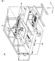
図14は、本発明の実施の形態に従う形状測定装置を備える塗布装置100の模式的な斜視図である。図14に示されるように、塗布装置100は、形状測定装置1Aと、塗布機構50とを備える。形状測定装置1Aは、被塗布対象物である基板15Aの形状を測定する。塗布機構50は、基板15Aに、塗布機構50に設けられた塗布針を用いて、基板15Aの被塗布対象面(上面側)に塗布材料を塗布し、回路パターンを描画する。
FIG. 14 is a schematic perspective view of
図15は、基板15Aの製造工程を示すフローチャートである。S51において塗布工程が行なわれる。塗布工程においては、基板15Aの被塗布面に回路パターンを描画する。S51に続いて、S52において形状測定工程が行なわれる。形状測定工程においては、形状測定装置1Aを用いて基板15Aの被塗布面の形状が測定される。S52に続いて、S53において検査工程が行なわれる。検査工程においては、S51において回路パターンが描画された被塗布面の形状を検査する。S53の終了により、基板15Aの製造工程が完了する。
FIG. 15 is a flowchart showing the manufacturing process of the
今回開示された実施の形態はすべての点で例示であって制限的なものではないと考えられるべきである。本発明の範囲は上記した説明ではなくて特許請求の範囲によって示され、特許請求の範囲と均等の意味および範囲内でのすべての変更が含まれることが意図される。 The embodiments disclosed this time are to be considered as illustrative in all points and not restrictive. The scope of the present invention is shown not by the above description but by the claims, and is intended to include meanings equivalent to the claims and all modifications within the scope.
1,1A 形状測定装置、2 光源、3 光源制御器、4 二光束干渉対物レンズ、5
観察光学系、6 撮像装置、6A 撮像面、7 Zステージ、8 Zステージ制御器、9 支持部材、10 ベース板、11 制御装置、12 キーボード、13 マウス、14 モニタ、15 被測定部品、15A 基板、21 レンズ、22 参照鏡、23 ビームスプリッタ、31 集光レンズ、32 ハーフミラー、33 結像レンズ、34 フィルタ、41 演算処理部、42 画像入力部、43 データ記憶部、44 位置制御値出力部、45 照明制御値出力部、50 塗布機構、100 塗布装置、Cxy 画素、D1a,D1b グラディエント、D2a,D2b ラプラシアン、E 曲線、EL,EZ 制御電圧、L1,L2 光、RAB 近接領域。
1, 1A shape measuring device, 2 light sources, 3 light source controller, 4 two-beam interference objective lens, 5
Observation optical system, 6 imaging device, 6A imaging surface, 7 Z stage, 8 Z stage controller, 9 support member, 10 base plate, 11 control device, 12 keyboard, 13 mouse, 14 monitor, 15 measured part, 15A substrate , 21 lens, 22 reference mirror, 23 beam splitter, 31 condensing lens, 32 half mirror, 33 imaging lens, 34 filter, 41 arithmetic processing unit, 42 image input unit, 43 data storage unit, 44 position control value output unit , 45 illumination control value output unit, 50 coating mechanism, 100 coating device, C xy pixel, D1a, D1b gradient, D2a, D2b Laplacian, E curve, EL, EZ control voltage, L1, L2 light, R AB proximity region.
Claims (5)
前記白色光を出力する光源と、
前記白色光を二光束に分離し、一方の光束を前記対象物に照射するとともに他方の光束を参照面に照射し、前記対象物からの反射光と前記参照面からの反射光とを干渉させて干渉光を出力するように構成される二光束干渉対物レンズと、
前記二光束干渉対物レンズから出力される干渉光の画像を取得するように構成される撮像装置と、
前記光源から出力された前記白色光を、前記二光束干渉対物レンズを介して前記対象物の表面に導き、前記表面からの反射光を前記二光束干渉対物レンズを介して前記撮像装置に導く観察光学系と、
前記二光束干渉対物レンズを前記対象物に対して相対的に移動させるように構成される位置決め装置と、
前記対象物と前記二光束干渉対物レンズとの距離を前記二光束干渉対物レンズの光軸方向に変化させながら複数の画像を取得し、前記複数の画像を用いて前記対象物の形状を測定するように構成される制御装置とを備え、
前記制御装置は、
前記複数の画像における各単位領域について、前記複数の画像にわたって輝度に基づく評価値が最大となる前記二光束干渉対物レンズの位置を当該単位領域の合焦位置として算出し、前記複数の画像における各単位領域の合焦位置に基づいて前記対象物の形状を測定し、
前記評価値として、前記複数の画像における各単位領域の輝度、および当該単位領域の輝度と当該単位領域に近接する複数の単位領域の輝度との差に相関関係のある値を用いるように構成され、
前記制御装置は、
前記複数の画像における各単位領域の輝度の最大値が閾値より大きい場合、前記輝度を前記評価値として用い、
前記最大値が前記閾値より小さい場合、前記差に相関関係のある値を前記評価値として用いる、形状測定装置。 A shape measuring device that irradiates an object with white light and measures the shape of the object using reflected light from the object,
A light source that outputs the white light,
The white light is separated into two light fluxes, one light flux is applied to the object and the other light flux is applied to the reference surface, and the reflected light from the object and the reflected light from the reference surface are caused to interfere with each other. And a two-beam interference objective lens configured to output interference light,
An imaging device configured to acquire an image of interference light output from the two-beam interference objective lens;
Observation in which the white light output from the light source is guided to the surface of the target object via the two-beam interference objective lens, and reflected light from the surface is guided to the imaging device via the two-beam interference objective lens. Optical system,
A positioning device configured to move the two-beam interference objective lens relative to the object;
A plurality of images are acquired while changing the distance between the object and the two-beam interference objective lens in the optical axis direction of the two-beam interference objective lens, and the shape of the object is measured using the plurality of images. And a control device configured as
The control device is
For each unit area in the plurality of images, the position of the two-beam interference objective lens having the largest evaluation value based on the luminance over the plurality of images is calculated as the focus position of the unit area, and each position in the plurality of images is calculated. Measuring the shape of the object based on the focus position of the unit area,
The evaluation value is configured to use a value having a correlation with the brightness of each unit area in the plurality of images, and the difference between the brightness of the unit area and the brightness of the plurality of unit areas adjacent to the unit area. ,
The control device is
When the maximum value of the brightness of each unit area in the plurality of images is larger than a threshold value, the brightness is used as the evaluation value,
Wherein when the maximum value is smaller than the threshold value, Ru with a value correlated to the difference as the evaluation value, the shape measuring device.
Priority Applications (5)
| Application Number | Priority Date | Filing Date | Title |
|---|---|---|---|
| JP2016021831A JP6680552B2 (en) | 2016-02-08 | 2016-02-08 | Shape measuring device and method of manufacturing object to be coated |
| US16/076,311 US10704898B2 (en) | 2016-02-08 | 2017-01-10 | Shape measuring apparatus and method for manufacturing target object to be coated |
| PCT/JP2017/000463 WO2017138281A1 (en) | 2016-02-08 | 2017-01-10 | Shape measuring device and method of manufacturing object to be coated |
| EP17750006.3A EP3415864B1 (en) | 2016-02-08 | 2017-01-10 | Shape measuring apparatus and method of manufacturing target object to be coated |
| CN201780010383.2A CN108603751B (en) | 2016-02-08 | 2017-01-10 | Shape measuring device and manufacturing method of target object to be coated |
Applications Claiming Priority (1)
| Application Number | Priority Date | Filing Date | Title |
|---|---|---|---|
| JP2016021831A JP6680552B2 (en) | 2016-02-08 | 2016-02-08 | Shape measuring device and method of manufacturing object to be coated |
Publications (2)
| Publication Number | Publication Date |
|---|---|
| JP2017142078A JP2017142078A (en) | 2017-08-17 |
| JP6680552B2 true JP6680552B2 (en) | 2020-04-15 |
Family
ID=59564061
Family Applications (1)
| Application Number | Title | Priority Date | Filing Date |
|---|---|---|---|
| JP2016021831A Expired - Fee Related JP6680552B2 (en) | 2016-02-08 | 2016-02-08 | Shape measuring device and method of manufacturing object to be coated |
Country Status (5)
| Country | Link |
|---|---|
| US (1) | US10704898B2 (en) |
| EP (1) | EP3415864B1 (en) |
| JP (1) | JP6680552B2 (en) |
| CN (1) | CN108603751B (en) |
| WO (1) | WO2017138281A1 (en) |
Families Citing this family (6)
| Publication number | Priority date | Publication date | Assignee | Title |
|---|---|---|---|---|
| JP2019152570A (en) * | 2018-03-05 | 2019-09-12 | 東芝メモリ株式会社 | measuring device |
| JP6867357B2 (en) * | 2018-11-09 | 2021-04-28 | 本田技研工業株式会社 | How to measure the amount of coating |
| DE102019114405A1 (en) * | 2019-05-29 | 2020-04-16 | Polytec Gmbh | Interferometric measuring device and interferometric method for determining the surface topography of a measurement object |
| CN110260783B (en) * | 2019-07-10 | 2020-11-10 | 中国工程物理研究院机械制造工艺研究所 | Automatic focusing device and method for interference microscope |
| CN115014210B (en) * | 2022-04-29 | 2025-02-18 | 深圳市中图仪器股份有限公司 | Compensation optical path structure for improving measurement accuracy |
| TW202509451A (en) * | 2022-10-14 | 2025-03-01 | 美商賽博光學股份有限公司 | Synchronous modulate, gate and integrate 3d sensor |
Family Cites Families (15)
| Publication number | Priority date | Publication date | Assignee | Title |
|---|---|---|---|---|
| JPH0399209A (en) * | 1989-09-12 | 1991-04-24 | Matsushita Electric Ind Co Ltd | Inspection apparatus for mounting board |
| JP3260425B2 (en) * | 1992-07-01 | 2002-02-25 | 日本アビオニクス株式会社 | Pattern edge line estimation method and pattern inspection device |
| JPH1062140A (en) * | 1996-08-14 | 1998-03-06 | Oki Electric Ind Co Ltd | Method and device for reconstruction of shape |
| US5784164A (en) * | 1997-03-20 | 1998-07-21 | Zygo Corporation | Method and apparatus for automatically and simultaneously determining best focus and orientation of objects to be measured by broad-band interferometric means |
| JP2000046651A (en) * | 1998-07-28 | 2000-02-18 | Sumitomo Electric Ind Ltd | Wire appearance inspection device |
| JP3610569B2 (en) * | 1999-03-23 | 2005-01-12 | 株式会社高岳製作所 | Active confocal imaging device and three-dimensional measurement method using the same |
| GB2395777B (en) * | 2002-11-27 | 2005-12-28 | Taylor Hobson Ltd | A surface profiling apparatus |
| JP4845607B2 (en) * | 2006-06-21 | 2011-12-28 | オリンパス株式会社 | Three-dimensional shape measuring method and apparatus |
| TWI336767B (en) * | 2007-07-05 | 2011-02-01 | Ind Tech Res Inst | Method for calibration of image and apparatus for acquiring image |
| JP5942847B2 (en) * | 2010-05-07 | 2016-06-29 | 株式会社ニコン | Height measuring method and height measuring apparatus |
| JP2013036848A (en) * | 2011-08-08 | 2013-02-21 | Nikon Corp | Height measuring device and method |
| JP5965167B2 (en) * | 2012-03-16 | 2016-08-03 | 株式会社ミツトヨ | White light interference measurement device |
| US8970850B2 (en) * | 2012-12-14 | 2015-03-03 | University Of New Brunswick | Method and apparatus for surface profilometry |
| JP6189102B2 (en) * | 2013-06-25 | 2017-08-30 | Ntn株式会社 | Coating apparatus and height detection method |
| JP6749814B2 (en) * | 2015-11-12 | 2020-09-02 | Ntn株式会社 | Height detection device and coating device equipped with the same |
-
2016
- 2016-02-08 JP JP2016021831A patent/JP6680552B2/en not_active Expired - Fee Related
-
2017
- 2017-01-10 WO PCT/JP2017/000463 patent/WO2017138281A1/en not_active Ceased
- 2017-01-10 CN CN201780010383.2A patent/CN108603751B/en not_active Expired - Fee Related
- 2017-01-10 US US16/076,311 patent/US10704898B2/en not_active Expired - Fee Related
- 2017-01-10 EP EP17750006.3A patent/EP3415864B1/en not_active Not-in-force
Also Published As
| Publication number | Publication date |
|---|---|
| CN108603751A (en) | 2018-09-28 |
| US20190049236A1 (en) | 2019-02-14 |
| CN108603751B (en) | 2020-09-01 |
| JP2017142078A (en) | 2017-08-17 |
| EP3415864A4 (en) | 2019-09-25 |
| EP3415864A1 (en) | 2018-12-19 |
| EP3415864B1 (en) | 2021-12-29 |
| US10704898B2 (en) | 2020-07-07 |
| WO2017138281A1 (en) | 2017-08-17 |
Similar Documents
| Publication | Publication Date | Title |
|---|---|---|
| JP6680552B2 (en) | Shape measuring device and method of manufacturing object to be coated | |
| JP6749814B2 (en) | Height detection device and coating device equipped with the same | |
| CN105301865B (en) | Automatic focusing system | |
| US20090216486A1 (en) | Method for measuring three-dimension shape | |
| CN106969704A (en) | Measuring system, measuring method, robot control method, robot, robot system and pick device | |
| JP6417645B2 (en) | Alignment method for surface profile measuring device | |
| JP2017096916A5 (en) | ||
| JP7093915B2 (en) | Surface shape measurement method | |
| JP2023176026A (en) | Method for determining scan range | |
| JP5096852B2 (en) | Line width measuring apparatus and inspection method of line width measuring apparatus | |
| JP5531883B2 (en) | Adjustment method | |
| US11326871B2 (en) | Height detection apparatus and coating apparatus equipped with the same | |
| CN107709923B (en) | Shape measuring device and coating device equipped with shape measuring device | |
| JP2017044473A (en) | measuring device | |
| JP4496149B2 (en) | Dimensional measuring device | |
| JP2007286284A (en) | Confocal scanning type microscopic system and observation method using the same | |
| GB2536604A (en) | Touch sensing systems | |
| JP2008046027A (en) | Method for measuring height and apparatus therefor |
Legal Events
| Date | Code | Title | Description |
|---|---|---|---|
| A621 | Written request for application examination |
Free format text: JAPANESE INTERMEDIATE CODE: A621 Effective date: 20190128 |
|
| A131 | Notification of reasons for refusal |
Free format text: JAPANESE INTERMEDIATE CODE: A131 Effective date: 20191105 |
|
| A521 | Request for written amendment filed |
Free format text: JAPANESE INTERMEDIATE CODE: A523 Effective date: 20191127 |
|
| TRDD | Decision of grant or rejection written | ||
| A01 | Written decision to grant a patent or to grant a registration (utility model) |
Free format text: JAPANESE INTERMEDIATE CODE: A01 Effective date: 20200225 |
|
| A61 | First payment of annual fees (during grant procedure) |
Free format text: JAPANESE INTERMEDIATE CODE: A61 Effective date: 20200319 |
|
| R150 | Certificate of patent or registration of utility model |
Ref document number: 6680552 Country of ref document: JP Free format text: JAPANESE INTERMEDIATE CODE: R150 |
|
| LAPS | Cancellation because of no payment of annual fees |