JP6668332B2 - Filter with improved linearity - Google Patents
Filter with improved linearity Download PDFInfo
- Publication number
- JP6668332B2 JP6668332B2 JP2017512698A JP2017512698A JP6668332B2 JP 6668332 B2 JP6668332 B2 JP 6668332B2 JP 2017512698 A JP2017512698 A JP 2017512698A JP 2017512698 A JP2017512698 A JP 2017512698A JP 6668332 B2 JP6668332 B2 JP 6668332B2
- Authority
- JP
- Japan
- Prior art keywords
- filter
- parallel
- series
- capacitor
- resonance
- Prior art date
- Legal status (The legal status is an assumption and is not a legal conclusion. Google has not performed a legal analysis and makes no representation as to the accuracy of the status listed.)
- Active
Links
- 239000003990 capacitor Substances 0.000 claims description 144
- 239000010410 layer Substances 0.000 claims description 24
- 230000005540 biological transmission Effects 0.000 claims description 18
- 239000000463 material Substances 0.000 claims description 11
- 230000001965 increasing effect Effects 0.000 claims description 8
- 239000004020 conductor Substances 0.000 claims description 5
- 239000002346 layers by function Substances 0.000 claims description 5
- 238000010897 surface acoustic wave method Methods 0.000 claims description 4
- 230000007423 decrease Effects 0.000 claims description 3
- 238000001465 metallisation Methods 0.000 claims description 3
- 238000009413 insulation Methods 0.000 claims description 2
- 230000008719 thickening Effects 0.000 claims description 2
- 239000000919 ceramic Substances 0.000 claims 1
- 238000011144 upstream manufacturing Methods 0.000 claims 1
- 230000000694 effects Effects 0.000 description 9
- 101150074474 VRP1 gene Proteins 0.000 description 8
- 238000000034 method Methods 0.000 description 6
- 230000008878 coupling Effects 0.000 description 5
- 238000010168 coupling process Methods 0.000 description 5
- 238000005859 coupling reaction Methods 0.000 description 5
- 101100098479 Caenorhabditis elegans glp-4 gene Proteins 0.000 description 4
- 230000008901 benefit Effects 0.000 description 4
- 230000001629 suppression Effects 0.000 description 4
- 239000011248 coating agent Substances 0.000 description 3
- 238000000576 coating method Methods 0.000 description 3
- 230000006866 deterioration Effects 0.000 description 3
- 238000004519 manufacturing process Methods 0.000 description 3
- 239000000758 substrate Substances 0.000 description 3
- 229910004298 SiO 2 Inorganic materials 0.000 description 2
- 230000008859 change Effects 0.000 description 2
- 238000013461 design Methods 0.000 description 2
- 230000001066 destructive effect Effects 0.000 description 2
- 239000000203 mixture Substances 0.000 description 2
- 238000013021 overheating Methods 0.000 description 2
- 230000009467 reduction Effects 0.000 description 2
- 230000004044 response Effects 0.000 description 2
- 230000035945 sensitivity Effects 0.000 description 2
- 101100165533 Arabidopsis thaliana BLH2 gene Proteins 0.000 description 1
- 101100476710 Saccharomyces cerevisiae (strain ATCC 204508 / S288c) SAW1 gene Proteins 0.000 description 1
- 230000002238 attenuated effect Effects 0.000 description 1
- UMIVXZPTRXBADB-UHFFFAOYSA-N benzocyclobutene Chemical compound C1=CC=C2CCC2=C1 UMIVXZPTRXBADB-UHFFFAOYSA-N 0.000 description 1
- 230000008033 biological extinction Effects 0.000 description 1
- 230000033228 biological regulation Effects 0.000 description 1
- 230000015556 catabolic process Effects 0.000 description 1
- 238000004891 communication Methods 0.000 description 1
- 230000000052 comparative effect Effects 0.000 description 1
- 238000012937 correction Methods 0.000 description 1
- 239000013078 crystal Substances 0.000 description 1
- 238000013016 damping Methods 0.000 description 1
- 238000006731 degradation reaction Methods 0.000 description 1
- 230000009977 dual effect Effects 0.000 description 1
- 238000005516 engineering process Methods 0.000 description 1
- 238000011156 evaluation Methods 0.000 description 1
- 230000002349 favourable effect Effects 0.000 description 1
- 230000006872 improvement Effects 0.000 description 1
- 238000010348 incorporation Methods 0.000 description 1
- 230000001939 inductive effect Effects 0.000 description 1
- 238000003780 insertion Methods 0.000 description 1
- 230000037431 insertion Effects 0.000 description 1
- 230000010354 integration Effects 0.000 description 1
- 230000002452 interceptive effect Effects 0.000 description 1
- 238000010030 laminating Methods 0.000 description 1
- 239000011159 matrix material Substances 0.000 description 1
- 238000005457 optimization Methods 0.000 description 1
- 229920000620 organic polymer Polymers 0.000 description 1
- 229920000642 polymer Polymers 0.000 description 1
- 229920006395 saturated elastomer Polymers 0.000 description 1
- 239000004065 semiconductor Substances 0.000 description 1
- 238000004088 simulation Methods 0.000 description 1
- 239000000126 substance Substances 0.000 description 1
- 230000002459 sustained effect Effects 0.000 description 1
- 239000010409 thin film Substances 0.000 description 1
- 238000012546 transfer Methods 0.000 description 1
Images


Classifications
-
- H—ELECTRICITY
- H03—ELECTRONIC CIRCUITRY
- H03H—IMPEDANCE NETWORKS, e.g. RESONANT CIRCUITS; RESONATORS
- H03H9/00—Networks comprising electromechanical or electro-acoustic devices; Electromechanical resonators
- H03H9/46—Filters
- H03H9/54—Filters comprising resonators of piezo-electric or electrostrictive material
- H03H9/542—Filters comprising resonators of piezo-electric or electrostrictive material including passive elements
-
- H—ELECTRICITY
- H03—ELECTRONIC CIRCUITRY
- H03H—IMPEDANCE NETWORKS, e.g. RESONANT CIRCUITS; RESONATORS
- H03H9/00—Networks comprising electromechanical or electro-acoustic devices; Electromechanical resonators
- H03H9/02—Details
- H03H9/02228—Guided bulk acoustic wave devices or Lamb wave devices having interdigital transducers situated in parallel planes on either side of a piezoelectric layer
-
- H—ELECTRICITY
- H03—ELECTRONIC CIRCUITRY
- H03H—IMPEDANCE NETWORKS, e.g. RESONANT CIRCUITS; RESONATORS
- H03H9/00—Networks comprising electromechanical or electro-acoustic devices; Electromechanical resonators
- H03H9/02—Details
- H03H9/02535—Details of surface acoustic wave devices
-
- H—ELECTRICITY
- H03—ELECTRONIC CIRCUITRY
- H03H—IMPEDANCE NETWORKS, e.g. RESONANT CIRCUITS; RESONATORS
- H03H9/00—Networks comprising electromechanical or electro-acoustic devices; Electromechanical resonators
- H03H9/46—Filters
- H03H9/54—Filters comprising resonators of piezo-electric or electrostrictive material
- H03H9/56—Monolithic crystal filters
- H03H9/566—Electric coupling means therefor
- H03H9/568—Electric coupling means therefor consisting of a ladder configuration
-
- H—ELECTRICITY
- H03—ELECTRONIC CIRCUITRY
- H03H—IMPEDANCE NETWORKS, e.g. RESONANT CIRCUITS; RESONATORS
- H03H9/00—Networks comprising electromechanical or electro-acoustic devices; Electromechanical resonators
- H03H9/46—Filters
- H03H9/54—Filters comprising resonators of piezo-electric or electrostrictive material
- H03H9/58—Multiple crystal filters
- H03H9/60—Electric coupling means therefor
- H03H9/605—Electric coupling means therefor consisting of a ladder configuration
-
- H—ELECTRICITY
- H03—ELECTRONIC CIRCUITRY
- H03H—IMPEDANCE NETWORKS, e.g. RESONANT CIRCUITS; RESONATORS
- H03H9/00—Networks comprising electromechanical or electro-acoustic devices; Electromechanical resonators
- H03H9/46—Filters
- H03H9/64—Filters using surface acoustic waves
- H03H9/6423—Means for obtaining a particular transfer characteristic
- H03H9/6433—Coupled resonator filters
- H03H9/6483—Ladder SAW filters
Description
通信工学及び電気音響学における相互変調(IM又はIMD)は、少なくとも2つの異なる周波数を処理しなくてはならない場合に、回路部品からの非線形伝達関数を介する不要な電波の発生を意味する。使用周波数範囲におけるこのような相互変調積は、不要な信号及び妨害を引き起こすことがあるため、混乱を生じる相互変調積の発生は常に回避するよう努められる。 Intermodulation (IM or IMD) in telecommunications and electroacoustics means the generation of unwanted radio waves via non-linear transfer functions from circuit components when at least two different frequencies have to be processed. Since such intermodulation products in the operating frequency range can cause unwanted signals and interference, it is always sought to avoid the occurrence of confusion intermodulation products.
HF信号発生時に、高調波も形成することがあり、またその周波数を合わせるのは、基本モードの偶数倍である必要がない。このような高調波は、基本モードから十分離れ得るが、それでも他の帯域を妨害する場合がある。通常、高調波も、f1及びf2が、f1=f2である特殊ケースの2つの周波数の相互変調積として現れることがある。 When the HF signal is generated, a harmonic may be formed, and the frequency need not be an even multiple of the fundamental mode. Such harmonics can be far enough away from the fundamental mode, but still disturb other bands. Normally, harmonics may also appear as intermodulation products of two special case frequencies where f1 and f2 are f1 = f2.
係数又は合計が異なり、混合積の基本周波数を含む、第二次、第三次及び高次の相互変調積又は高調波がある。 There are second, third and higher order intermodulation products or harmonics that differ in the coefficients or sums and contain the fundamental frequency of the mixing product.
相互変調積及び混乱を生じる高調波を回避するために、成分及び回路部品の直線性の向上が最初に求められる場合がある。これが達成しないと、回路素子が直線的に対応する範囲を広げるために、非直線性成分にかかる電圧を下げることとなる。 In order to avoid intermodulation products and harmonics that cause confusion, an increase in the linearity of the components and circuit components may be required first. If this is not achieved, the voltage on the non-linear component will be reduced in order to widen the range of circuit elements that correspond linearly.
フィルター技術の領域、特に直列及び並列共振回路のネットワークから構成される、リアクタンスフィルターにおいて、複数の共振部をカスケード接続することにより相互変調積を抑制することができるが、完全に除去することはできない。カスケード接続の欠点は、共振部の回路構成における、フィルターに必要な静電容量であり、つまり、共振部のカスケード接続は、各コンデンサー又は共振部の空き容量条件を増加することによってのみ持続及び適応することができる。結果として、カスケード接続を増加させた共振部フィルターの空き容量条件は過大であり、従ってカスケード接続は不経済となる。さらに、これは小型化への要求に逆らう。 In the field of filter technology, in particular, in a reactance filter composed of a network of series and parallel resonance circuits, intermodulation products can be suppressed by cascading a plurality of resonance units, but cannot be completely eliminated. . The disadvantage of cascading is the capacitance required for the filter in the circuit configuration of the resonator, i.e. the cascading of the resonators is only sustained and adapted by increasing the free space requirements of each capacitor or resonator. can do. As a result, the free space requirement of the resonator filter with increased cascading is excessive, thus making cascading uneconomical. Furthermore, this goes against the demand for miniaturization.
さらなる欠点は、カスケード接続の増加により飽和効果が生じ、そのため、カスケード接続への共振部の追加にかかわらずその効果が出ない、又は、達成し得る相互変調積及び高調波の抑制が、追加の共振部の使用で、より小さくなってしまうことである。 A further disadvantage is that the increased cascading results in a saturation effect, so that despite the addition of the resonating part to the cascading, the effect is not achieved, or the intermodulation products and harmonic suppression that can be achieved are at an additional level. The use of the resonating part results in a smaller size.
図9は、カスケード接続のn度に応じて、第二次高調波(IMD2)及び第三次高調波(IMD3)の相互変調積抑制がどのように現れるかを示し、このnは直列接続する共振部の数を示す。直線箇所の増加、曲線箇所の減少が、飽和状態を明確に表す。これは、カスケード接続が、特定の角度においてのみ技術的及び経済的に実現可能であることを示す。 FIG. 9 shows how the intermodulation product suppression of the second harmonic (IMD2) and the third harmonic (IMD3) appears depending on n degrees of cascade connection, where n is connected in series. Shows the number of resonance units. An increase in the number of straight lines and a decrease in the number of curves clearly indicate the saturated state. This shows that cascading is technically and economically feasible only at certain angles.
本発明の目的は、直線性を改善し、相互変調積及び高調波の抑制を行うフィルター回路を明示することである。さらに、フィルター回路は、共振部表面積の適度な増加を実現すべきである。 It is an object of the present invention to specify a filter circuit that improves linearity and suppresses intermodulation products and harmonics. Further, the filter circuit should achieve a modest increase in the surface area of the resonator.
本目的は、請求項1に記載の特徴を有するフィルター回路による本発明に従い達成する。本発明の有利な実施形態は、追加の請求項により明示される。
This object is achieved according to the invention by a filter circuit having the features of
フィルター回路は、リアクタンスフィルターとして形成される第一フィルターを含む。このようなフィルターは、第一フィルターポートと第二フィルターポートとの間に接続する、直列信号経路(直列枝)を含む。並列枝は、固定電位の回路ノードに接続する直列信号経路に配置される各回路ノードから分岐する。少なくとも1つの共振部又は1つの共振部の回路構成は、直列枝及び各並列枝に配置される。 The filter circuit includes a first filter formed as a reactance filter. Such filters include a serial signal path (series branch) connecting between the first filter port and the second filter port. The parallel branch branches from each circuit node arranged in a series signal path connected to the circuit node having the fixed potential. At least one resonating part or a circuit configuration of one resonating part is arranged on the series branch and each parallel branch.
リアクタンスフィルターは、直列枝の回路ノード又は共振部との接続ポートから開始することができる。 The reactance filter can be started from the connection node with the circuit node or the resonance unit of the series branch.
フィルターポートの1つに最も近く配置、又は、直列枝のフィルターポートに直接接続、あるいは、[missing]された、少なくとも第一並列枝において、複数の共振部は、直列又は並列で複数の共振部の直列回路構成と接続する第一コンデンサーと直列接続し、その結果、第一ケースでは電圧分割、第二ケースでは電流分割を生じる。 In at least the first parallel branch, arranged closest to one of the filter ports, or directly connected to, or missing from, the filter ports of the series branch, the plurality of resonators are connected in series or in parallel. As a result, voltage division occurs in the first case and current division occurs in the second case.
従って、本発明の根本概念は、少なくとも1つの線形要素を含む、電圧デバイダ又は電流デバイダ回路を提供することである。上記のコンデンサーは、好ましくは線形要素であるが、電圧分割に適する他の線形要素であってもよい。この方法によって最初に述べた飽和を低減することが可能であり、そうでなければ、カスケード率の増加に伴い、すなわち、直列接続の共振部の数が増加することで、相互変調積の回避効果が低減され続けることとなる。コンデンサーはさらに、比較的広帯域で作動し、故に広域周波数帯域に適応する電圧分割又は電力分割効果という利点を有する。電圧分割の場合、以下のケースとなる。線形要素になる電圧が大きくなるほど、相互変調積の低減への影響が大きくなる。直列又は並列枝の総静電容量に比べて、コンデンサーの容量がより小さくなれば、効果がより大きくなり、かつ、相互変調積及び高調波の発生をより強力に回避する。 Accordingly, the underlying concept of the present invention is to provide a voltage divider or a current divider circuit including at least one linear element. The capacitors described above are preferably linear elements, but may be other linear elements suitable for voltage division. This method makes it possible to reduce the first mentioned saturation, otherwise it is possible to avoid intermodulation products as the cascade ratio increases, i.e. by increasing the number of resonators connected in series. Will continue to be reduced. Capacitors also have the advantage of operating over a relatively wide band and, thus, a voltage or power dividing effect that adapts to a wide frequency band. In the case of voltage division, the following case occurs. The greater the voltage that becomes a linear element, the greater the effect on reducing the intermodulation products. The smaller the capacitance of the capacitor compared to the total capacitance of the series or parallel branches, the greater the effect and the stronger the avoidance of intermodulation products and the generation of harmonics.
共振部の回路構成に並列接続、つまり、共振部との直列カスケード接続するコンデンサーは電流デバイダの代わりになる。より大きな電流が線形要素を流れると、非線形要素には電流がわずかしか流れず、本発明に従う相互変調積又は高調波の発生がほとんどなくなるという場合もある。 A capacitor connected in parallel to the circuit configuration of the resonance unit, that is, in series cascade connection with the resonance unit, replaces the current divider. When a larger current flows through the linear element, only a small amount of current may flow through the non-linear element, and there may be little generation of intermodulation products or harmonics according to the present invention.
線形要素は通常フィルター回路内に配置され単独で機能する。しかし線形要素は、少なくとも1つの信号が信号経路へ発信又は接続するフィルターポートに最も近いこれらの共振部に並列接続又は直列接続することで最大の効果を有し、かつ、それ自身、又は、非線形要素での異なるシステム周波数にて相互変調積及び高調波を形成することができる。全体として、回路環境にカップリングが依存しないため、このフィルターポートはフィルター入力又はフィルター出力となる場合があり、従って、クライアント特有で、かつ、フィルター回路などに依存しない。本発明に従い、線形要素は、この「第一」共振部にどの場合も接続する。第一ノード及び「第一」並列アームが並列共振部のフィルターポートにより近い場合、「第一」共振部は、直列共振部などであってよい。 Linear elements are usually located in the filter circuit and function alone. However, a linear element has the greatest effect by being connected in parallel or in series to these resonators that are closest to the filter port where at least one signal originates or connects to the signal path, and is itself or non-linear. Intermodulation products and harmonics can be formed at different system frequencies at the element. As a whole, since the coupling does not depend on the circuit environment, this filter port may be a filter input or a filter output, and is therefore client-specific and independent of the filter circuit and the like. According to the invention, a linear element is in each case connected to this "first" resonator. If the first node and the "first" parallel arm are closer to the filter port of the parallel resonator, the "first" resonator may be a series resonator or the like.
線形コンデンサーは、平板コンデンサーとして共通回路基板上の共振部と共に容易に実現することができる。しかし、別々の外部要素として共振部にコンデンサーを接続することも可能である。しかしながら、これに関して、共通回路基板上の統合は、さらなる利点を有する。フィードバック要素として共振部に接続することもできるインダクタンスに比べて、コンデンサーはその使用時に、追加の共振部、及び、フィルターの伝播挙動における追加の混乱が起こらず、コンデンサーを利用して電圧分割又は電力分割の影響が広帯域にて達成することが可能であるという利点を有する。 A linear capacitor can be easily realized as a flat plate capacitor together with a resonance section on a common circuit board. However, it is also possible to connect a capacitor to the resonator as a separate external element. However, in this regard, integration on a common circuit board has further advantages. Compared to the inductance, which can also be connected to the resonator as a feedback element, the capacitor, when used, does not cause additional resonance and additional disruption in the propagation behavior of the filter, and uses the capacitor to divide voltage or power. It has the advantage that the effect of division can be achieved in a wide band.
提示されたフィルター回路の1つの欠点は、電圧分割又は電力分割にて共振部のゼロピッチが減少し、これがフィルターの帯域幅に直接影響することである。フィルターの最適化により、所望の帯域幅を定めることができ、同時に欠点も考慮しなければならないが、通過帯域、特にVSWRや阻止帯域付近では、フィルター挙動は容易に減衰することができる。 One drawback of the proposed filter circuit is that the voltage division or power division reduces the zero pitch of the resonator, which directly affects the bandwidth of the filter. By optimizing the filter, the desired bandwidth can be defined and at the same time disadvantages must be taken into account, but the filter behavior can be easily attenuated in the passband, especially near the VSWR and stopband.
本発明に従い最適化された第一フィルターにより提示されたフィルター挙動は、優れた透過挙動又はVSWR、及び、相互変調積又は高調波との間の相反関係を示す。混乱を生じる相互変調積又は高調波の混乱を回避するか、若しくは、最適化された透過挙動又はVSWRをさらに重視するかどうかについても評価すべきである。 The filter behavior exhibited by the first filter optimized according to the invention shows a good transmission behavior or VSWR, and a reciprocal relationship between the intermodulation products or harmonics. One should also evaluate whether to avoid disrupting intermodulation products or harmonics, or to place more emphasis on optimized transmission behavior or VSWR.
本発明に従う好ましい影響は既に達成されたが、これは、単一共振部が、第一直列枝又は並列枝のコンデンサーに直列又は並列に接続する場合である。共振部の静電容量及びコンデンサーの容量を合わせると、直列枝又は並列枝の総容量となる。両方とも、フィルター設計において考慮されなければならない。 The favorable effect according to the invention has already been achieved, when a single resonator is connected in series or in parallel to a capacitor in the first series or parallel branch. When the capacitance of the resonance unit and the capacitance of the capacitor are combined, the total capacitance of the series branch or the parallel branch is obtained. Both must be considered in filter design.
好ましい実施形態においては、共振部は音波と共に用いるよう設計される。従って、SAW、FBAR、又はBAW(弾性表面波(Surface Acoustic Wave)、薄膜バルク音響波(Thin Film Bulk Acoustic Wave)、又はバルク音響波(Bulk Acoustic Wave))は、フィルター回路又はフィルター回路の第一フィルターに適している。ガイドバルク波と共に発振するGBAW(ガイドバルク音響波(Guided Bulk Acoustic Wave))共振部も適応する。いかなる場合でも、共振部の容量は共振部表面積によって設定される。第一板状電極と第二板状電極との間の重複範囲に、特に圧電性物質がそれらとの間に配設される限りにおいては、BAW共振部の共振部表面が配置される。SAW共振部では、静電容量は、共振部の開口積及び共振部の電極指数の関数である。 In a preferred embodiment, the resonator is designed for use with sound waves. Therefore, SAW, FBAR, or BAW (Surface Acoustic Wave, Thin Film Bulk Acoustic Wave, or Bulk Acoustic Wave) is the first of a filter circuit or a filter circuit. Suitable for filters. A GBAW (Guided Bulk Acoustic Wave) resonator that oscillates with the guide bulk wave is also applicable. In any case, the capacitance of the resonator is set by the surface area of the resonator. The resonator surface of the BAW resonator is disposed in the overlapping range between the first plate electrode and the second plate electrode, particularly as long as the piezoelectric substance is disposed therebetween. In a SAW resonator, the capacitance is a function of the aperture area of the resonator and the electrode index of the resonator.
原則として、共振部はLC共振部として設計することができるが、並列枝内で、又はその並列枝に並列して、相互接続することにより、相互変調積又は高調波の低減もまた達成することが可能である。 In principle, the resonators can be designed as LC resonators, but also achieve a reduction of intermodulation products or harmonics by interconnecting in or parallel to the parallel branches. Is possible.
実施可能な実施形態の1つにおいて、第一並列枝の共振部の回路構成は、直列する4つから8つの回路構成を含む。相互変調積又は高調波の十分な減衰性を有する優れた透過挙動は、この数を適当な空き容量条件に使用することで達成される。他の実施形態は、回路構成により多くの又はより少ない共振部を含むことができる。 In one possible embodiment, the circuit configuration of the resonance unit of the first parallel branch includes four to eight circuit configurations in series. Excellent transmission behavior with sufficient damping of intermodulation products or harmonics is achieved by using this number for appropriate free space conditions. Other embodiments may include more or fewer resonators in the circuit configuration.
さらなる実施形態では、第二コンデンサーは、追加の直列又は並列共振部に、直列又は並列に接続される。この第二コンデンサーは任意であり、コンデンサー自身はほとんどが線形要素であるのに対して、さらなる個々の電圧降下を引き起こして非線形要素となる。相互変調積又は高調波もこのようにして低減される。 In a further embodiment, the second capacitor is connected in series or parallel to an additional series or parallel resonator. This second capacitor is optional and, while the capacitor itself is mostly a linear element, causes additional individual voltage drops to become a non-linear element. Intermodulation products or harmonics are also reduced in this way.
第二コンデンサーもまた、混乱又は相互変調積を生じる1つの信号を接続することにより、可能な限りフィルターポートに付近に配設される。 A second capacitor is also placed as close as possible to the filter port by connecting one signal that causes confusion or intermodulation products.
対応共振部が、直列共振部である場合、「並列接続」とは、第二コンデンサーを共振部の前後にある側枝の回路ノードに通じる並列経路内に配設することを意味する。 When the corresponding resonance unit is a series resonance unit, “parallel connection” means that the second capacitor is disposed in a parallel path leading to a circuit node on a side branch before and after the resonance unit.
対応共振部が並列共振部である場合、第二コンデンサーは、有利に共振部を含む並列枝に隣接し、かつ、共振部を有する並列枝としての直列信号経路にある同様の回路ノードに特に接続する並列枝に配設される。 If the corresponding resonating part is a parallel resonating part, the second capacitor is preferably connected to a similar circuit node which is advantageously adjacent to the parallel branch containing the resonating part and in the series signal path as a parallel branch having the resonating part. Arranged in parallel branches.
有利な実施形態では、第一フィルターは、フィルター入力又はフィルター出力に接続する複数の送信ブランチを含むフィルター回路の受信フィルターである。送信ブランチは、異なる伝送帯域にて送信するよう設計されているので、受信フィルターの通過帯域内に好ましくない通信がある場合に生じことがあり、また、このようなフィルター回路にて、相互変調積が理論上生じる場合がある。フィルター内で使用される信号外の異なる周波数の相互接続又は周波数のカップリングが容量性経路、誘導性経路、抵抗性経路又は電磁経路にて起こることがあり、これは完全には回避ができない。しかし、カップリングのさらなる結果である、非線形要素の結果としての相互変調積又は高調波は、本発明にむしろ低減することが可能である。 In an advantageous embodiment, the first filter is a receiving filter of a filter circuit comprising a plurality of transmitting branches connected to a filter input or a filter output. Since the transmission branch is designed to transmit in a different transmission band, it may occur when there is undesired communication in the pass band of the reception filter. May theoretically occur. Interconnection of different frequencies or frequency coupling outside the signals used in the filter can occur in capacitive, inductive, resistive or electromagnetic paths, which cannot be completely avoided. However, the intermodulation products or harmonics as a result of the non-linear element, which is a further consequence of the coupling, can be rather reduced in the present invention.
さらなる実施形態では、第一フィルターは受信フィルターとして設計される。これは、他の発信又は受信フィルターを含むフィルター回路の一部となることがある。 In a further embodiment, the first filter is designed as a receiving filter. This can be part of a filter circuit that includes other transmit or receive filters.
第一フィルターは複数の送信ブランチを含むフィルター回路の一部であるデュプレクサ又はマルチプレクサの一部になる場合があり、それらの信号は、フィルターの信号経路に接続することができる。 The first filter may be part of a duplexer or multiplexer that is part of a filter circuit that includes a plurality of transmission branches, and their signals may be connected to the signal path of the filter.
本発明のさらなる実施形態では、第一共振部の前、最後の共振部の後に設置され、かつ、信号経路内に配設される各共振部との間に追加的に、又は、2つの共振部毎の間に常に設置され、若しくは、信号経路内に配設される共振部の全回路構成との間に配置される。追加的なコンデンサーは、共振部又はカスケード接続された共振部の回路構成に接続されることがある。 According to a further embodiment of the invention, in addition to, or between, two resonances, each of which is arranged before the first resonance, after the last resonance and arranged in the signal path. It is always installed between each unit, or is installed between the entire circuit configuration of the resonance unit arranged in the signal path. The additional capacitor may be connected to the resonating part or the cascaded resonating part circuit configuration.
第一フィルターは、フィルター素子としての共振部だけを含み得る。しかし、信号経路内で、DMSフィルターと接続することが可能である。これは、直列信号経路内の回路ノードがDMSフィルターの入力に接続され、かつ、さらなる回路ノードはDMSフィルターの出力に接続されるという容易な方法により達成する。DMSフィルターは有利にフィルター入力に隣接しないが、2つの共振部の間、又は直列信号経路内の共振部の2つの回路構成の間に配置される。 The first filter may include only a resonance part as a filter element. However, it is possible to connect with a DMS filter in the signal path. This is achieved in an easy way, wherein circuit nodes in the series signal path are connected to the input of the DMS filter, and further circuit nodes are connected to the output of the DMS filter. The DMS filter is advantageously not adjacent to the filter input, but is located between the two resonators or between the two circuit configurations of the resonators in the series signal path.
既に述べたように、フィルター基板内に組み込まれるコンデンサーを搭載する実施形態は、特に有利であることを示している。共振部は、音波と共に用いるよう設計され、かつ、共通チップ上に配設される。第一コンデンサー及び/又は第二コンデンサー及び/又は追加の第一第二コンデンサーは、同じチップ上に平板コンデンサーとして導入される。このような平板コンデンサーは、2つの平状キャパシタ電極とそれらとの間に配設される誘電体層を有する。本明細書の平板デザインは、印刷導体より断面積が非常に大きいことを意味する。 As already mentioned, embodiments incorporating a capacitor integrated into the filter substrate have shown to be particularly advantageous. The resonator is designed for use with sound waves and is disposed on a common chip. The first condenser and / or the second condenser and / or the additional first second condenser are introduced as plate capacitors on the same chip. Such a flat capacitor has two flat capacitor electrodes and a dielectric layer disposed between them. The flat design herein means that the cross-sectional area is much larger than the printed conductor.
チップ素子の追加機能層と合わさる誘電体層が、単一工程にて製造される場合は、優れた組み込み性に利点となる。このようにして、コンデンサー又はコンデンサーの誘導体に積層、又はこれらを作成する公知のフィルターの製造に既に使用されている手段が使用できる。 If the dielectric layer to be combined with the additional functional layer of the chip element is manufactured in a single step, it is advantageous for excellent incorporation. In this way, the means already used for the production of known filters for laminating or for producing capacitors or capacitor derivatives can be used.
一般的に、機能層及び誘電体層の組み合わせ製造は、両方が同じ材料、及び、同じコーティング厚を有することを意味する。しかし、次の工程にて機能層又は誘電体層を厚くすること、又は、コーティングの厚みを薄くすることが可能である。いかなる場合でも、特に高い厚み制御性を特徴とする、できる限り高い直線性を有するコンデンサーを製造することが重要である。 In general, the combined production of a functional layer and a dielectric layer means that both have the same material and the same coating thickness. However, it is possible to increase the thickness of the functional layer or the dielectric layer or to reduce the thickness of the coating in the next step. In any case, it is important to produce capacitors with as high a linearity as possible, characterized in particular by a high thickness controllability.
1つの実施形態は、2つの伝導路の交差領域にて、伝導路を絶縁するために、第一フィルター又はフィルター回路内の他の場所で使用される誘電体として有機ポリマーを有する。ベンゾシクロブテンをベースにしたポリマー類及びその誘導体類は、実績があり、かつ有益な材料である。半導体回路に実績のある本材料は、低誘電率を有し、均一な多層厚を容易に製造することができる。 One embodiment has an organic polymer as a dielectric that is used elsewhere in the first filter or filter circuit to insulate the conductive path at the intersection of the two conductive paths. Benzocyclobutene-based polymers and their derivatives are proven and useful materials. This material, which has a proven track record in semiconductor circuits, has a low dielectric constant and can be easily manufactured with a uniform multilayer thickness.
さらなる実施形態では、中周波数の過昇温反応の補正、つまり、中周波数の過昇温の温度係数のために、材料は公知のフィルターに使用される誘電体層として使用される。通常、機械的特性の正特性を有する材料層、特にSiO2がこのために使用される。本発明に従い、このSiO2層は、誘電体層として使用することができ、そのコーティング厚は、コンデンサーの最適な静電容量値、又は温度係数の最適な補正値、若しくはこの2つのトレードオフのどれかを提供するよう最適化することができる。 In a further embodiment, the material is used as a dielectric layer to be used in known filters, to compensate for the medium frequency overheating response, ie the temperature coefficient of the medium frequency overheating. Usually, a layer of material having positive mechanical properties, in particular SiO 2, is used for this. According to the invention, this SiO 2 layer can be used as a dielectric layer, the coating thickness of which can be determined by the optimal capacitance value of the capacitor, or the optimal correction value of the temperature coefficient, or the trade-off between the two. It can be optimized to provide any.
一般的に、機械的特性の正特性を有する他の材料も、本目的のために使用することができる。誘導体層の作成後、コンデンサーの上部電極は、誘導体層上で印加されなければならない。 In general, other materials with positive mechanical properties can also be used for this purpose. After creation of the dielectric layer, the top electrode of the capacitor must be applied on the dielectric layer.
さらなる実施形態では、フィルターの別の場所や、別の方法に既に使用されている材料も、平板コンデンサーの電極に有利に使用される。 In a further embodiment, materials already used elsewhere in the filter or in other methods are also advantageously used for the electrodes of the plate capacitor.
例えば、コンデンサーの下部電極は、共振部として使用されるSAW1ポート共振部の金属化から形成することができるコンデンサーの上部電極は、例えばフィルターの端子パッド上に形成されるパッドの厚みと共に形成することができる。 For example, the lower electrode of the capacitor can be formed from the metallization of the SAW1 port resonator used as the resonator. The upper electrode of the capacitor can be formed with the thickness of the pad formed, for example, on the terminal pad of the filter. Can be.
線形化コンデンサーが電子音響共振部の通常の電極構造体を有することが可能である。コンデンサーはその共振周波数に離調する場合がある。疑似SAW共振部又は疑似GBAW共振部は、基板の結晶軸に対応して回転することができるため、電気音響結合係数k2は十分に低いという可能性もある。 It is possible that the linearizing capacitor has the usual electrode structure of the electroacoustic resonator. The capacitor may detune to its resonance frequency. Pseudo SAW resonator section or pseudo GBAW resonating portion, it is possible to rotate in response to the crystal axis of the substrate, the electro-acoustic coupling coefficient k 2 is fully possible that low.
本発明に従う1つのフィルター回路にて、相互変調積又は高調波が結合する結果となる少なくとも1つの信号によって明白な効果を示すコンデンサーは、フィルターポート近辺に配設される。共振部のカスケード接続についても同様であり、好ましくは、フィルター入力に直接又は近隣にあるそれらの共振部を特に実行する。 In one filter circuit according to the present invention, a capacitor which exhibits a pronounced effect by at least one signal resulting from the coupling of intermodulation products or harmonics is arranged near the filter port. The same is true for the cascading of the resonators, preferably implementing those resonators directly or adjacent to the filter input.
従って、有利なフィルター回路は、共振部及び複数の共振部の回路構成を有し、1つの実施形態では、回路構成は、カスケード接続した共振部の複数の共振部及び共振部のカスケード率を含み、フィルター入力から離れるに伴いこのフィルター回路が縮小する。このようにして、増加するカスケード率に並列する、増加するフィルター回路の空き容量条件に制限をすることは可能である。 Thus, an advantageous filter circuit has a circuit configuration of a resonating unit and a plurality of resonating units, and in one embodiment, the circuit configuration includes a plurality of resonating units of a cascaded resonating unit and a cascade ratio of the resonating units. , The filter circuit shrinks as one moves away from the filter input. In this way, it is possible to limit the free space requirements of the increasing filter circuit in parallel with the increasing cascade rate.
本発明に従うフィルターは、並列枝の最適化数値を含み得る。有利には、2〜7、具体的には2〜4の並列枝が提供される。本発明に従うフィルターは、並列枝の最適化数値を含み得る。直列要素は、直列共振部の回路構成として、あるいは、DMSフィルター又はDMS基板などの別の要素としての直接共振部である。第二コンデンサーは、直列要素の一部でもあり得る。直列要素は、回路ノードによって両側に接する。1つの直列要素は、都度、フィルター入力とフィルター回路ノードとの間に、又は、フィルター出力とフィルター出力との間に配設することができる。有利には、2〜6の直列要素が提供される。 A filter according to the invention may include optimized values for parallel branches. Advantageously, 2 to 7, in particular 2 to 4 parallel branches are provided. A filter according to the invention may include optimized values for parallel branches. The series element is a direct resonance section as a circuit configuration of the series resonance section or another element such as a DMS filter or a DMS substrate. The second capacitor can also be part of a series element. The series elements are flanked by circuit nodes. One series element can be arranged each time between the filter input and the filter circuit node or between the filter output and the filter output. Advantageously, two to six series elements are provided.
各共振部若しくは直列枝又は並列枝へ線形化要素を追加することは必要ではない。通常、要素を、効果が高い線形稼動のコンデンサーなどの定位置に接続することで十分である。基本信号及び/又は干渉信号が通過帯域に位置するかどうかに応じて、回路トポロジーにおける要素の理想的な位置は変更することがある。 It is not necessary to add a linearization element to each resonator or series branch or parallel branch. Usually, it is sufficient to connect the element to a fixed position, such as a highly efficient linearly operated condenser. Depending on whether the fundamental signal and / or the interfering signal is located in the passband, the ideal location of the elements in the circuit topology may change.
本発明はさらなる詳細を例示的実施形態及び添付図で参照し、以下で説明する。図がフィルター及びフィルター回路を表す限りにおいては、これらは単に概略的な説明を意味する。これは、提示される各フィルター回路は、フィルターのさらなる最適化のために、不可欠ではないがフィルター回路に使用することができる、それ自体公知の他の要素を含み得ることも意味する。本発明に無関係である要素は削除することができる。 The present invention is described below with reference to further details in exemplary embodiments and the accompanying drawings. To the extent that the figures depict filters and filter circuits, these merely mean a schematic description. This also means that each filter circuit presented can include other elements known per se, which can, but need not, be used in the filter circuit for further optimization of the filter. Elements that are not relevant to the present invention can be omitted.
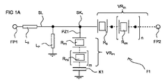
図1Aは、本発明の簡略的かつ典型的な実施形態を示している。図1Aに示すのは、直列信号線SLにより第一フィルターポートFP1と第二フィルターポートFP2とが接続されているフィルター回路のフィルターである。第一フィルターポートFP1及び第二フィルターポートFP2は、任意選択により、フィルター入力又はフィルター出力に割り当てることができる。信号線SLには、直列共振部RS1が配置されている。任意選択により、信号経路SL内の第一直列共振部RS1に、追加の共振部RSXを接続することができる。Nは、0〜約10の整数値を表し得る。直接直列接続された直列共振部により、共振部VRS1の第一回路構成が形成される。全ての共振部RSXは、それぞれ異なる特性(共振周波数又は静電容量等)を有する。 FIG. 1A shows a simplified and exemplary embodiment of the present invention. FIG. 1A shows a filter of a filter circuit in which a first filter port FP1 and a second filter port FP2 are connected by a serial signal line SL. The first filter port FP1 and the second filter port FP2 can be optionally assigned to a filter input or a filter output. The series resonance section RS1 is arranged on the signal line SL. Optionally, an additional resonator RSX can be connected to the first series resonator RS1 in the signal path SL. N may represent an integer value from 0 to about 10. The first circuit configuration of the resonance unit VRS1 is formed by the series resonance units directly connected in series. All the resonance units RSX have different characteristics (resonance frequency, capacitance, etc.).
直列共振部の前後に、回路ノードSKを備えることができる。回路ノードSKには、他の要素、フィルター分岐、又は信号経路を接続することができる。図1Aにおいて、第一並列分岐PZ1は、第一回路ノードSK1から分岐し、第一回路ノードSK1と固定電位とを接続する。ここでは、固定電位はフレーム電位である。第一並列分岐PZ1に、第一並列共振部RP1が配置されている。第一並列分岐PZ1は、任意選択により、直列接続されたm個の他の並列共振部RPXに直列接続されている。値mは、nとは独立して選択され、同様の値をとることができる。これらの並列共振部により、回路構成VRP1が形成される。第一コンデンサーK1は、並列共振部と固定電位との相互接続部に直列接続されている。共振部RPXの特性(共振周波数又は静電容量等)は互いに異なり、RSXの特性とも異なる。 A circuit node SK can be provided before and after the series resonance unit. Other elements, filter branches, or signal paths can be connected to the circuit node SK. In FIG. 1A, a first parallel branch PZ1 branches from a first circuit node SK1, and connects the first circuit node SK1 to a fixed potential. Here, the fixed potential is a frame potential. The first parallel resonance part RP1 is arranged in the first parallel branch PZ1. The first parallel branch PZ1 is optionally connected in series to m other parallel resonance units RPX connected in series. The value m is selected independently of n and can have similar values. A circuit configuration VRP1 is formed by these parallel resonance units. The first capacitor K1 is connected in series to an interconnect between the parallel resonance unit and the fixed potential. The characteristics (resonance frequency or capacitance, etc.) of the resonance unit RPX are different from each other, and also different from the characteristics of the RSX.
任意選択により、信号線SLに追加の受動素子を一体化又は接続することができる。例えば、フィルターポートFP1と第一回路ノードSK1との間に、直列インダクタンスLSを一体化させることができる。あるいは、第一フィルターポートFP1と第一共振部RS1との間の回路ノードから、並列コイルLPをグランドに接続することができる。 Optionally, additional passive elements can be integrated or connected to the signal line SL. For example, the series inductance LS can be integrated between the filter port FP1 and the first circuit node SK1. Alternatively, the parallel coil LP can be connected to the ground from a circuit node between the first filter port FP1 and the first resonance unit RS1.
追加の直列コイルLS及び/又は追加の並列コイルLPは、第二フィルターポートFP2側に備えることができる。 An additional series coil LS and / or an additional parallel coil LP can be provided on the second filter port FP2 side.
指標n及びmは回路のカスケード率を決定するものである。そのため、1〜約10の整数値をとる。原理上、指標n及びmは大きな値をとることができる。ただし、そのような高いカスケード率が、フィルター回路に必要な面という理由により経済的に又は技術的に意味を為さない場合は、n及びmは互いに異なるように選択することができる。図1Aには、信号線SL内の他の回路ノードによってグランドに接続され得る追加の並列分岐は、示されていない。また、直列共振部の追加の回路を、2つのそのような回路ノードSKの間に備えることができる。 The indices n and m determine the cascade rate of the circuit. Therefore, it takes an integer value of 1 to about 10. In principle, the indices n and m can take large values. However, if such a high cascade ratio does not make sense economically or technically because of the necessary aspects of the filter circuit, n and m can be chosen differently. FIG. 1A does not show additional parallel branches that may be connected to ground by other circuit nodes in signal line SL. Also, an additional circuit of the series resonator can be provided between two such circuit nodes SK.
第一コンデンサーK1のないフィルター回路と比較すると、図1Aのフィルター回路を使用することにより、特定の相互変調積を約10dB低減、又は、約10dB改善することができる。図1A及び後出の図では、フィルター回路内に存在し得る追加の要素(特に、追加の並列分岐、追加の共振部、又は直列共振部の追加の回路構成)が省略されている。直列及び/又は並列インダクタンスを、信号線に備える又は連結することができる。 By using the filter circuit of FIG. 1A, the specific intermodulation product can be reduced by about 10 dB or improved by about 10 dB when compared to a filter circuit without the first capacitor K1. In FIG. 1A and the following figures, additional elements that may be present in the filter circuit (especially additional parallel branches, additional resonators, or additional circuit configurations of series resonators) are omitted. Series and / or parallel inductances can be provided or coupled to the signal lines.
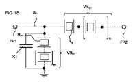
図1Bは、他の典型的な実施形態を示している。図1Aと比較すると、図1Bの実施形態では、第一コンデンサーK1は、並列共振部VRP1の回路に直列接続されておらず、第一並列分岐PZ1内でこの回路に並列接続されている。そのため、並列接続されたこの第一コンデンサーK1により、信号線内の回路ノードと固定電位とが接続されている。この実施形態においても、相互変調積を最大10dB低減することができる。 FIG. 1B shows another exemplary embodiment. Compared to FIG. 1A, in the embodiment of FIG. 1B, the first capacitor K1 is not connected in series to the circuit of the parallel resonance part VRP1, but is connected in parallel to this circuit in the first parallel branch PZ1. Therefore, the circuit node in the signal line and the fixed potential are connected by the first capacitor K1 connected in parallel. Also in this embodiment, the intermodulation product can be reduced by a maximum of 10 dB.
図1Cは、本発明の追加の実施形態を示している。図1Cは、図1Aに類似するように設計されている。ただし、この場合、第二コンデンサーK2は、第一並列分岐PZ1が分岐する第一回路ノードSK1と、直列共振部VRS1の第一回路構成との間で、直列分岐SL内で相互接続されている。このように第二コンデンサーK2が信号線において分圧部として機能している場合でも、同じ数の共振部RS、RPを有するがコンデンサーを有しない公知のフィルター回路と比べて、フィルター回路の線形性は向上する。また、図1A及び図1Bを参照して説明した拡張の可能性は、この構造にも当てはまる。 FIG. 1C shows an additional embodiment of the present invention. FIG. 1C is designed to be similar to FIG. 1A. However, in this case, the second capacitor K2 is interconnected in the series branch SL between the first circuit node SK1 from which the first parallel branch PZ1 branches and the first circuit configuration of the series resonance unit VRS1. . As described above, even when the second capacitor K2 functions as a voltage divider in the signal line, the linearity of the filter circuit is smaller than that of a known filter circuit having the same number of resonance units RS and RP but having no capacitor. Improves. The extension possibilities described with reference to FIGS. 1A and 1B also apply to this structure.
図1Dは、図1Cに類似の実施形態を示している。図1Dでは、信号線SL内の第一回路ノードSK1が第一共振部RS1又は直列共振部VRS1の第一回路構成の後方に配置され、第二コンデンサーK2が第一共振部RS1又は第一回路構成VRSと第一フィルターポートFP1との間に備えられている。第一回路ノードSK1と第二フィルターポートFP2との間には、直列共振部の追加の回路構成VRSを備えることができる。また、追加の並列分岐が接続された追加の回路ノードSKを備えることができる。更に、別の直列の第二コンデンサーK2を、各2つの回路ノードの間に備えることができる。固定電位と並列共振部の回路構成との間に配置されるように、追加の第一コンデンサーK1を各並列分岐に追加的に備えることができる。 FIG. 1D shows an embodiment similar to FIG. 1C. In FIG. 1D, the first circuit node SK1 in the signal line SL is arranged behind the first circuit configuration of the first resonance unit RS1 or the series resonance unit VRS1, and the second capacitor K2 is connected to the first resonance unit RS1 or the first circuit. The configuration is provided between the VRS and the first filter port FP1. An additional circuit configuration VRS of the series resonance unit may be provided between the first circuit node SK1 and the second filter port FP2. Further, an additional circuit node SK to which an additional parallel branch is connected can be provided. Furthermore, another series second capacitor K2 can be provided between each two circuit nodes. An additional first capacitor K1 can be additionally provided for each parallel branch, so as to be arranged between the fixed potential and the circuit configuration of the parallel resonance section.
図1Eは、図1Dに類似のフィルター回路を示している。ここで、第二コンデンサーK2は、第一回路構成VRS又は直列共振部VRSに並列に配置されている。第一回路ノードSK1に接続された第一並列分岐PZは、並列共振部の回路構成VRP1を有する。直列共振部VRS1の第一回路と第二フィルターポートFP2との間には、直列共振部VRSの追加の回路構成を少なくとも1つ備えることができる。直列共振部VRの回路構成の両側で、並列分岐が各回路ノードSKに接続し得る。 FIG. 1E shows a filter circuit similar to FIG. 1D. Here, the second capacitor K2 is arranged in parallel with the first circuit configuration VRS or the series resonance unit VRS. The first parallel branch PZ connected to the first circuit node SK1 has a circuit configuration VRP1 of a parallel resonance unit. At least one additional circuit configuration of the series resonance unit VRS can be provided between the first circuit of the series resonance unit VRS1 and the second filter port FP2. On both sides of the circuit configuration of the series resonance part VR, parallel branches can be connected to each circuit node SK.
第二コンデンサーK2が直列信号線において分圧を行う本実施形態においても、フィルター回路の線形性が向上し、相互変調積/高調波の出現が低減される。 Also in the present embodiment in which the second capacitor K2 performs voltage division in the serial signal line, the linearity of the filter circuit is improved, and the appearance of intermodulation products / harmonics is reduced.
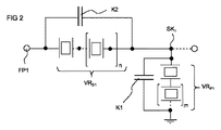
図2は、第一コンデンサーK1が並列共振部VRPの回路構成に並列接続され、かつ、第二コンデンサーK2が直列共振部VRSの回路構成に並列接続された、フィルター回路を示している。信号線VRS1内の直列共振部の回路構成及び第一並列分岐PZ1内の並列共振部SRPの回路構成は、それぞれコンデンサーK1、K2でブリッジされている。 FIG. 2 shows a filter circuit in which the first capacitor K1 is connected in parallel to the circuit configuration of the parallel resonance unit VRP, and the second capacitor K2 is connected in parallel to the circuit configuration of the series resonance unit VRS. The circuit configuration of the series resonance unit in the signal line VRS1 and the circuit configuration of the parallel resonance unit SRP in the first parallel branch PZ1 are bridged by capacitors K1 and K2, respectively.
図3は、信号線SLに備えられた第二コンデンサーK2及び第一並列分岐PZ1に並列接続された第一コンデンサーK1が相互接続されている実施形態を示している。フィルター回路は、追加の直列共振部又は直列共振部の追加の回路構成、及び追加の共振部又は並列共振部の追加の回路構成が配置されている追加の並列分岐を含み得る。 FIG. 3 shows an embodiment in which the second capacitor K2 provided on the signal line SL and the first capacitor K1 connected in parallel to the first parallel branch PZ1 are interconnected. The filter circuit may include an additional series resonator or an additional circuit configuration of the series resonator, and an additional parallel branch where an additional circuit configuration of the additional resonator or the parallel resonator is arranged.
図4は、図3に類似のフィルター回路を示している。ただし、第一コンデンサーK1は、並列共振部RP又は並列共振部VRPの回路構成に並列に配置されている。 FIG. 4 shows a filter circuit similar to FIG. However, the first capacitor K1 is arranged in parallel with the circuit configuration of the parallel resonance unit RP or the parallel resonance unit VRP.
図5は、図4に類似のフィルター回路を示している。ただし、第一コンデンサーK1は、並列共振部RP又は並列共振部VRPの回路構成に直列に配置されている。 FIG. 5 shows a filter circuit similar to FIG. However, the first capacitor K1 is arranged in series with the circuit configuration of the parallel resonance unit RP or the parallel resonance unit VRP.
図示されていない実施形態では、フィルター回路は並列分岐から始まる。一方、図1D〜図6では全て直列共振部又は直列共振部の回路構成から始まる。「から始まる」とは、入力として機能するフィルターポートの最も近くに配置されている共振部のことを意味する。 In an embodiment not shown, the filter circuit starts with a parallel branch. On the other hand, FIG. 1D to FIG. "Begins with" means the resonating portion located closest to the filter port functioning as an input.
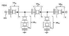
図6は、信号線SL内に直列共振部VRSの回路構成が3つ配置されたフィルター回路を示している。このような回路構成2つ毎に、回路ノードSKが備えられ、その間に配置されている。この各回路ノードSKから、いずれの場合にも、並列分岐PZには対応する並列共振部VRPの回路構成が備えられている。 FIG. 6 illustrates a filter circuit in which three circuit configurations of the series resonance unit VRS are arranged in the signal line SL. A circuit node SK is provided for every two such circuit configurations, and is disposed therebetween. From each of the circuit nodes SK, in any case, the parallel branch PZ is provided with a circuit configuration of the corresponding parallel resonance unit VRP.
第二コンデンサーK2が、各フィルター入力と直列共振部の第一回路構成との間と、直列共振部の第一回路構成と第二回路構成との間と、直列共振部の第二回路構成と第三回路構成との間とに備えられている。 The second capacitor K2 is connected between each filter input and the first circuit configuration of the series resonance unit, between the first circuit configuration of the series resonance unit and the second circuit configuration, and the second circuit configuration of the series resonance unit. A third circuit configuration is provided.
対応する並列共振部の回路構成を有する並列分岐PZは、共振部VRSの各2つの直列回路構成の間において、グランドに向かって延びている。 A parallel branch PZ having a corresponding parallel resonant circuit configuration extends towards ground between each two series circuit configurations of the resonant portion VRS.
直列共振部VRSの回路構成のカスケード率を示す指標n、o、pは個別に選択され、1〜10の値をとることができる。並列共振部VRPの回路構成のカスケード率を特定する指標m、kも、1〜10の値をとることができる。インターバルの下側領域における直列の回路構成及び並列の回路構成のカスケード率は、好ましくは適切な各指標が1〜7の値を有するように、より好ましくは1〜5の値を有するように選択される。 The indices n, o, and p indicating the cascade ratio of the circuit configuration of the series resonance unit VRS are individually selected and can take values of 1 to 10. The indices m and k for specifying the cascade ratio of the circuit configuration of the parallel resonance unit VRP can also take values of 1 to 10. The cascade ratio of the series circuit configuration and the parallel circuit configuration in the lower region of the interval is preferably selected such that each suitable index has a value of 1 to 7, more preferably 1 to 5. Is done.
図7は、特定の回路環境又はある実際のシステム要件に応じて設計され、かつ、相互変調積を最大限低減させるために設計された、実際のフィルター回路を図示している。ここで、直列信号線SLは、例えば、3つの回路ノードSK1、SK2、SK3を有している。この3つの回路ノードSK1、SK2、SK3からは、それぞれ、並列分岐PZがグランドに向かって分岐している。また、DMSフィルターDMSが、第三並列分岐の後方で信号線に直列接続されている。 FIG. 7 illustrates a real filter circuit designed for a particular circuit environment or certain real system requirements and designed to minimize intermodulation products. Here, the serial signal line SL has, for example, three circuit nodes SK1, SK2, and SK3. From each of the three circuit nodes SK1, SK2, and SK3, a parallel branch PZ branches toward the ground. Also, a DMS filter DMS is connected in series to the signal line behind the third parallel branch.
第二回路ノードSK2と第三回路ノードSK3との間には、直列共振部の第二直列回路構成VRS2が配置されている。DMSフィルターDMSと第二フィルターポートFP2との間には、非カスケード直列共振部RS1が備えられている。 A second series circuit configuration VRS2 of a series resonance unit is arranged between the second circuit node SK2 and the third circuit node SK3. A non-cascade series resonance unit RS1 is provided between the DMS filter DMS and the second filter port FP2.
このようなフィルター回路は、例えば、公称通過帯域2620MHz〜2630MHzに対応するように設計されている。フィルター回路の一部である本発明のこのフィルターと、既知の技術によって構成されているが本発明のフィルターに可能な限り類似させたフィルターとを比較するために、7個の相互接続された並列共振部を有する第一並列分岐と、直列共振部の二重カスケード回路構成と、2個の並列共振部を有する第二並列分岐と、直列共振部と、DMSフィルターと、追加の直列共振部と、2個の並列共振部の二重カスケード回路構成とを含む参照用フィルターが設計された。 Such a filter circuit is designed, for example, to correspond to a nominal pass band of 2620 MHz to 2630 MHz. To compare this filter of the present invention, which is part of a filter circuit, with a filter constructed according to known techniques but as similar as possible to the filter of the present invention, seven interconnected parallels are used. A first parallel branch having a resonance unit, a double cascade circuit configuration of a series resonance unit, a second parallel branch having two parallel resonance units, a series resonance unit, a DMS filter, and an additional series resonance unit. A reference filter was designed that included a dual cascade circuit configuration of two parallel resonators.
図7に示す本発明のフィルターと上述の参照用フィルターとを比較すると、通過帯域の位置と帯域幅が、両フィルターで同じであることが分かった。本発明のフィルターにおいては、通過帯域における挿入損失に関する劣化が最小限であり、阻止帯域付近における劣化減衰もわずかである。定在波比VSWRを示すマトリクスパラメータS11及びS22でさえも、劣化がわずかな値を示す。 Comparing the filter of the present invention shown in FIG. 7 with the above-mentioned reference filter, it was found that the position and the bandwidth of the pass band were the same for both filters. In the filter of the present invention, the deterioration related to the insertion loss in the pass band is minimized, and the deterioration attenuation near the stop band is also small. Even the matrix parameters S11 and S22 indicating the standing wave ratio VSWR show slight degradation.
参照用フィルターにおいて周波数2690MHzで発生する破壊的な三次相互変調積は、本発明のフィルターにおいては低減されており、その低減の程度は10dBを超える。フィルター特性の実質的な変更やわずかな劣化もなく、相互変調積の抑制による改善が顕著であったことから、本発明により得られるメリットが明らかとなった。本発明の成果は、次の点でも見られる。本発明のようにコンデンサーが接続されていない既知の技術のフィルターにおいて、相互変調積を同様に低減するためには、第一並列共振部のカスケード率は13とされる。このような高いカスケード率では、追加で必要となる面が大きすぎるため、問題外である。そのため、現実的な用途から除外される。本発明を利用することにより、非常に小さい面において同じ結果を得ることができる。 The destructive third-order intermodulation products occurring at a frequency of 2690 MHz in the reference filter are reduced in the filter of the present invention, and the degree of the reduction exceeds 10 dB. The improvement obtained by suppressing the intermodulation products was remarkable without any substantial change or slight deterioration of the filter characteristics, and the advantages obtained by the present invention became clear. The results of the present invention are also seen in the following points. In the filter of the known technique in which no capacitor is connected as in the present invention, the cascade ratio of the first parallel resonance section is set to 13 in order to similarly reduce the intermodulation products. Such a high cascade ratio is out of the question because the additional required surface is too large. Therefore, it is excluded from practical use. By utilizing the present invention, the same results can be obtained on very small surfaces.
図8は、図7に示すフィルターを使用して、破壊的な相互変調積の発生又は消滅をどのように実証することができるかを示す。このために、例えば、図7のフィルターの入力に、特定の周波数範囲f1及び10dBmの強さの第一干渉音が加えられる。第二干渉周波数は、2500MHz〜2570MHzの周波数範囲f2で変化して、フィルター入力に同様に加えられる。この第二干渉信号の強さは、5dBmである。 FIG. 8 shows how the use of the filter shown in FIG. 7 can be used to demonstrate the occurrence or extinction of destructive intermodulation products. For this purpose, for example, a first interference sound with a specific frequency range f1 and an intensity of 10 dBm is added to the input of the filter of FIG. The second interference frequency varies in the frequency range f2 from 2500 MHz to 2570 MHz and is similarly applied to the filter input. The strength of this second interference signal is 5 dBm.
典型的なシステム要件によると、三次相互変調積の評価は、一定の周波数fIMD=2690MHz=2*f2−f1で行わなければならない。図8に、この方法を使用して図7のフィルターで測定された第一グラフG1を示す。第二グラフG2は、同じ方法でテストされた比較用フィルターを示す。ただし、比較用フィルターは、第一並列分岐に第一コンデンサーがない状態で実施されている。図8では、周波数に対して、対応する三次相互変調積の減衰がプロットされている。 According to typical system requirements, the evaluation of the third-order intermodulation product must be made at a constant frequency f IMD = 2690 MHz = 2 * f2-f1. FIG. 8 shows a first graph G1 measured with the filter of FIG. 7 using this method. The second graph G2 shows a comparative filter tested in the same way. However, the comparison filter is implemented without the first condenser in the first parallel branch. In FIG. 8, the attenuation of the corresponding third-order intermodulation product is plotted against frequency.
図8を参照すると、第二グラフG2と比べて、本発明のフィルターのグラフG1では、特に相互変調積が最大となる臨界周波数2570MHzにおいて、発生する相互変調積に対する抑制が約10dB向上していることが分かる。第三グラフG3は、第一並列分岐に第一コンデンサーがない状態で実施されているフィルター構成の性能を示している。ただし、このフィルター構成においては、カスケード接続された並列共振部の数が、上述の周波数2570において相互変調積を同じように抑制できる数まで増加されている。これは、カスケード率が13のときにのみ可能であり、つまり、13個の並列共振部の回路構成であることを意味する。
Referring to FIG. 8, compared to the second graph G2, in the graph G1 of the filter of the present invention, the suppression of the generated intermodulation product is improved by about 10 dB especially at the
これは、第一並列分岐に4個のカスケード接続された並列共振部を有する本発明のフィルターと比較して、必要なフィルター面が大幅に減少することを意味する。上述した参照用フィルターの相対音響空間要件は、1.0である。本発明のフィルターの相対音響空間要件は、1.6である。一方、カスケード率13を有するフィルター(図8中のグラフG3に対応)の相対音響空間要件は、2.8である。これは、上述の本発明のフィルターと比較すると、1.8倍増加した相対音響空間要件に対応する。あるいは、言い換えると、本発明によれば、対象のfIMDにおいて同じ抑制を行うと、音響空間要件を1.8倍削減することができる。 This means that the required filter area is greatly reduced compared to a filter according to the invention having four cascaded parallel resonators in the first parallel branch. The relative acoustic space requirement of the above-mentioned reference filter is 1.0. The relative acoustic space requirement of the filter of the present invention is 1.6. On the other hand, the relative acoustic space requirement of the filter having the cascade ratio 13 (corresponding to the graph G3 in FIG. 8) is 2.8. This corresponds to a 1.8-fold increase in relative acoustic space requirements when compared to the inventive filter described above. Or, in other words, according to the present invention, performing the same suppression in the target f IMD can reduce the acoustic space requirement by a factor of 1.8.
フィルター回路に、2つより多い強い干渉信号が発生することが考えられる。スマートフォンの4つの異なる周波数(2×セル方式、2×WLAN)で最大4つの同時発生的な強い伝送信号が予想される方向において、標準化が行われている。その結果、周波数が受信帯域内に位置する、複数の可能な追加の非線形混合物が発生し得る。これにより、受信感度が著しく減少する。この複数の可能な追加の非線形混合物についても、本発明によれば大幅に低減することができる。これにより、これらのあらゆる場合において、受信感度が向上したフィルターが提供される。 It is possible that more than two strong interference signals are generated in the filter circuit. Standardization is being carried out in a direction in which up to four simultaneous strong transmission signals are expected at four different frequencies (2 × cell system, 2 × WLAN) of the smartphone. As a result, a number of possible additional non-linear mixtures, whose frequencies lie within the reception band, may occur. This significantly reduces the receiving sensitivity. This plurality of possible additional non-linear mixtures can also be significantly reduced according to the invention. This provides a filter with improved receiving sensitivity in all of these cases.
最初に説明した通り、カスケード率を変更した場合、カスケード接続された共振部の静電容量を調整してバランスをとる必要がある。図7に示すような、第一並列分岐において直列接続された4個の共振部及び第一コンデンサーK1を有する本発明のフィルターの場合、直列又は並列共振部の直列回路構成(カスケード)における全ての共振部が、同じ静電容量CS,Rを有することで可能となり、好ましい。 As described first, when the cascade ratio is changed, it is necessary to adjust the capacitance of the cascade-connected resonance units to achieve a balance. As shown in FIG. 7, in the case of the filter of the present invention having four resonance units and the first capacitor K1 connected in series in the first parallel branch, all filters in the series circuit configuration (cascade) of the series or parallel resonance units are used. This is possible because the resonance section has the same capacitance CS and R , which is preferable.
通例、m個の共振部がカスケード接続されている場合、このカスケードの総静電容量CS,R,gesは、CS,R,ges=CS,R/mとなる。このカスケードに直列接続されたコンデンサーKは、以下の容量CKを有する。
CK=a*CS,R,ges,
このとき、1以上の量が選択されるものとする。
カスケード及びコンデンサーからの容量CS,gesamtは、以下で表される。
CS,gesamt CK/(a+1)
それぞれが静電容量CS,Rを有するm個の共振部のカスケードにコンデンサーが並列接続されている実施形態では、このカスケードの総静電容量は、CS,R/mでCS,R,gesとなる。
Normally, when m resonance units are cascaded, the total capacitance CS, R, ges of this cascade is CS, R, ges = CS , R / m. Condenser K connected in series with the cascade has the following capacity C K.
C K = a * C S, R, ges,
At this time, one or more amounts are selected.
The capacitance CS, gesamt from the cascade and the condenser is expressed as:
C S, gesamt C K / ( a + 1)
In an embodiment where a capacitor is connected in parallel to a cascade of m resonators each having a capacitance CS, R , the total capacitance of this cascade is CS , R / m and CS, R. , Ges .
このカスケードに並列接続されたコンデンサーKは、容量CK=b*CS,R,ges=b/m*CS,Rを有する。このとき、bも、1以上の値が選択されるものとする。 The capacitors K connected in parallel in this cascade have a capacity C K = b * CS, R, ges = b / m * CS , R. At this time, it is assumed that one or more values of b are selected.
カスケード及びこのカスケードに並列なコンデンサーによる容量CS,gesamtは、以下で表される。
CS,gesamt=CK *(1+b)/b
The capacitance C S, gesamt of the cascade and the capacitors in parallel with this cascade is expressed as:
C S, gesamt = C K * (1 + b) / b
本発明のフィルターにおける容量を測定するために、異なった好ましい測定方法が適用される2つの一般的な場合AとBとに区別することができる。 In order to measure the volume in the filter according to the invention, a distinction can be made between two general cases A and B where different preferred measuring methods are applied.
場合Aでは、フィルターは、カスケードVRS接続された直列共振部及びこの直列共振部に直列又は並列接続された第二コンデンサーK2から始まる。後続の第一並列分岐PZ1にも、第一コンデンサーK1に直列又は並列接続された共振部のカスケードVRP1が含まれる。直列分岐には、カスケードVRS2接続された追加の直列共振部が存在する。少なくとも1つの追加の並列分岐PZが、共振部の追加のカスケードVRP2を含む。 In case A, the filter starts with a series resonator connected in cascade VRS and a second capacitor K2 connected in series or parallel to this series resonator. The subsequent first parallel branch PZ1 also includes a cascade VRP1 of resonance units connected in series or in parallel to the first capacitor K1. In the series branch there is an additional series resonance connected in cascade VRS2. At least one additional parallel branch PZ includes an additional cascade VRP2 of resonators.
ラダー型フィルター又はサブフィルターの全ての並列分岐の総容量は、接続されているコンデンサーの有無に関わらず、ほぼ同じサイズとなるように選択されなければならない。ただし、第二フィルターポートFP2における最後の並列分岐又はフィルター出力に限っては例外である。最後の並列分岐は、最終の並列分岐であり得る。直列分岐では、これ以上音響要素が(信号方向に)後続することはない。 The total capacitance of all parallel branches of the ladder-type filter or sub-filter must be chosen to be approximately the same size, with or without a connected capacitor. The exception is the last parallel branch or filter output at the second filter port FP2. The last parallel branch may be the last parallel branch. In a series branch, no more acoustic elements follow (in the signal direction).
前記コンデンサーを含む第二コンデンサーに接続された直列共振部の第一カスケードの総容量は、直列分岐における追加のカスケードVRS2の総容量の約2倍となるように計算することが好ましい。ただし、第二フィルターポートFP2の最後の直列共振部又はフィルター出力に限っては例外である。最後の直列共振部は、最終の直列共振部であり得る。並列分岐では、これ以上音響要素が(信号方向に)後続することはない。 Preferably, the total capacity of the first cascade of the series resonator connected to the second capacitor including the capacitor is calculated to be about twice the total capacity of the additional cascade VRS2 in the series branch. However, the exception is limited to the last series resonance part or the filter output of the second filter port FP2. The last series resonator may be the last series resonator. In a parallel branch, no more acoustic elements follow (in the signal direction).
場合Bでは、フィルターは、第一コンデンサーK1に直列又は並列接続された共振部のカスケードVRP1を含む並列分岐から始まる。この後方に、直列分岐において、カスケードVRS接続された直列共振部及びこの直列共振部に直列又は並列接続されたコンデンサーK2が続く。直列分岐には、カスケードVRS2接続された追加の直列共振部も存在する。少なくとも1つの追加の並列分岐PZが、共振部のカスケードVRP2を含む。 In case B, the filter starts with a parallel branch comprising a cascade VRP1 of resonators connected in series or in parallel to the first capacitor K1. This is followed, in the series branch, by a series resonator connected in cascade VRS and a capacitor K2 connected in series or in parallel to this series resonator. In the series branch there is also an additional series resonance connected in cascade VRS2. At least one additional parallel branch PZ includes a cascade VRP2 of resonators.
この場合、ラダー型フィルター又はサブフィルターの全てのカスケードの総容量(第二コンデンサーの有無に関わらず)がほぼ同じサイズとなるように選択されなければならない。ただし、第二フィルターポートFP2の最後又は最終の直列共振部又はフィルター出力に限っては例外である。第一コンデンサー(コンデンサーK1を含む)に接続された並列共振部の第一カスケードVRP1の総容量は、並列分岐における追加のカスケードVRP2の総容量の約半分となるように計算することが好ましい。ただし、第二フィルターポートFP2の最後の又は最終の並列分岐又はフィルター出力に限っては例外である。
以下に本願の出願当初の特許請求の範囲に記載された発明を付記する。
[C1]
第一フィルター(F1)を含むフィルター回路であって、
−直列信号経路(SL)により第一フィルターポート(IN)と第二フィルターポート(OUT)とが接続されており、
−回路ノード(SK)が直列信号経路内に配置され、前記回路ノード(SK)はそれぞれ並列分岐(PZ)を介して固定電位に接続されており、
−共振部(RS、RP)又は共振部の回路構成(VRS、VRP)が、直列分岐及び前記並列分岐に配置されており、
−前記フィルター入力(IN)の最も近くに配置された第一並列分岐(PZ1)は、並列共振部又は直列接続された複数の並列共振部の回路構成を含み、
−第一直列共振部、又は直列接続された複数の共振部の第一回路構成が、信号経路(SP)内に含まれ、かつ、前記フィルター入力(IN)の最も近くに配置されており、
−第一コンデンサー(K1)が、前記第一並列分岐(PZ1)に直列又は並列接続されている、及び/又は、第二コンデンサー(K2)が、前記第一直列共振部、又は直列接続されている複数の共振部の前記第一回路構成に直列又は並列接続されている、フィルター回路。
[C2]
前記共振部は、音波によって動作する共振部として設計されている、[C1]に記載のフィルター回路。
[C3]
前記第一並列分岐における共振部の回路構成は、1個〜8個の直列の共振部の回路構成を含む、[C1]又は[C2]に記載のフィルター回路。
[C4]
第二コンデンサー(K2)は、前記第一直列共振部又は直列共振部の第一回路構成(VRS1)と前記第一フィルターポート(FP1)との間において、直列信号経路に接続されている、又は、直列信号経路に並列にされており、
第一コンデンサー(K1)は、前記第一並列共振部(RP1)、又は前記第一並列分岐(PZ1)における並列共振部の第一回路構成(VRP1)に直列又は並列接続されている、[C1]〜[C3]のいずれか一項に記載のフィルター回路。
[C5]
前記第一フィルター(F1)は送信フィルター又は受信フィルターであり、
前記フィルター回路は、第一又は第二フィルターポート(FP1、FP2)に連結された1つ以上の受信分岐又は送信分岐を追加的に含み、前記送信分岐は異なる送信周波数帯域で送信を行うように設計され、前記受信分岐は異なる受信周波数帯域で受信を行うように設計されている、[C1]〜[C4]のいずれか一項に記載のフィルター回路。
[C6]
前記第一フィルター(F1)は、送受切換器の受信フィルター又は送信フィルターである、[C1]〜[C5]のいずれか一項に記載のフィルター回路。
[C7]
−前記フィルターは、第二コンデンサー(K2)が直列又は並列接続された直列共振部又は直列共振部(RS)の回路構成(VRS1)から始まり、
−並列共振部の回路構成及びこの回路構成に並列又は直列接続されたコンデンサーの回路構成の容量の結果として、並列分岐はそれぞれ同じ総容量を有しており、
−前記信号線における最後又は最終の並列分岐は、前記総容量に関するこの規定から除外される、[C1]〜[C6]のいずれか一項に記載のフィルター回路。
[C8]
−前記フィルターは第一並列分岐(PZ1)から始まり、前記第一並列分岐(PZ1)においては、並列共振部又は並列共振部の回路構成(VRP1)が第一コンデンサー(K1)に直列又は並列接続されており、
−直列共振部の回路構成及びこの回路構成に並列又は直列接続された第二コンデンサー(K2)の容量の結果として、直列共振部又は直列共振部(RS)の回路構成(VRS)はそれぞれ同一の総容量を有しており、
−前記信号経路における最後又は最終の直列共振部、又は直列共振部の最後又は最終の回路構成は、前記総容量に関するこの規定から除外される、[C1]〜[C6]のいずれか一項に記載のフィルター回路。
[C9]
第二コンデンサー(K2)は、いずれの場合にも、前記第一共振部の前、前記最後の共振部の後、及び信号経路(SL)に配置された全ての共振部の間に配置されている、[C1]〜[C8]のいずれか一項に記載のフィルター回路。
[C10]
前記信号経路(SL)には、DMSフィルター(DMS)が直列接続されている、[C1]〜[C9]のいずれか一項に記載のフィルター回路。
[C11]
前記フィルター回路はチップ部品として設計されており、
−前記共振部が、SAWシングルポート共振部として設計されており、
−前記共振部が、1つの共通のチップ上に配置されており、
−前記チップ上の第一及び/又は第二コンデンサー(K1、K2)は平板コンデンサーとして実現されており、前記平板コンデンサーは2つの平板コンデンサー電極を有し、前記2つの平板コンデンサー電極は、前記2つの平板コンデンサー電極の間に配置されたストリップ導体及び誘電体層に対向しており、
−前記誘電体層と、前記チップ部品の追加の機能層とは、1つの製造工程で作成され、同じ材料及び同じ層厚を有しており、
−前記コンデンサーの下部電極は、前記シングルポート共振部のメタライゼーションにより形成され、
−前記コンデンサーの上部電極は、前記フィルターの端子パッド上に作成されるパッドの肥厚化により形成される、[C1]〜[C10]のいずれか一項に記載のフィルター回路。
[C12]
−前記コンデンサー電極の間の前記誘電体層は、前記フィルター回路の交差するストリップ導体部分間の絶縁に使用される絶縁層と共に作成される、[C11]に記載のフィルター回路。
[C13]
−前記コンデンサー電極間の面全体に形成された層は、機械特性、特に剛化性について温度係数が正である材料を有する前記フィルター回路の温度係数を最小化する誘電体層として機能し、コンデンサーの領域では、前記上部コンデンサー電極が、前記コンデンサーの領域内の前記誘電体層に追加的に形成されている、[C11]に記載のフィルター回路。
[C14]
コンデンサーは、前記第一フィルターを有する前記チップのラダー型回路として設計されておらず、LTCCに一体化されている、又は、外部のディスクリートコンデンサーとして積層体に一体化されている、[C1]〜[C10]のいずれか一項に記載のフィルター回路。
[C15]
共振部構成には、複数のカスケード接続された共振部が含まれており、
前記フィルター回路内の前記共振部のカスケード率は、前記フィルター入力からの距離が増加するにつれ減少する、[C1]〜[C14]のいずれか一項に記載のフィルター回路。
In this case, the total capacity (with or without the second condenser) of all cascades of the ladder-type filter or the sub-filter must be selected to be of approximately the same size. However, the exception is limited to the last or last series resonance part of the second filter port FP2 or the filter output. Preferably, the total capacity of the first cascade VRP1 of the parallel resonator connected to the first capacitor (including the capacitor K1) is calculated to be about half of the total capacity of the additional cascade VRP2 in the parallel branch. The exception is the last or last parallel branch or filter output of the second filter port FP2.
Hereinafter, the invention described in the claims at the time of filing the application of the present application is additionally described.
[C1]
A filter circuit including a first filter (F1),
The first filter port (IN) and the second filter port (OUT) are connected by a series signal path (SL);
The circuit nodes (SK) are arranged in a serial signal path, each said circuit node (SK) being connected to a fixed potential via a parallel branch (PZ);
The resonance unit (RS, RP) or the circuit configuration of the resonance unit (VRS, VRP) is arranged in the series branch and the parallel branch,
The first parallel branch (PZ1) located closest to the filter input (IN) comprises a circuit configuration of a parallel resonance unit or a plurality of parallel resonance units connected in series;
The first series resonator, or the first circuit configuration of the plurality of resonators connected in series, is included in the signal path (SP) and is disposed closest to the filter input (IN); ,
A first capacitor (K1) is connected in series or in parallel with the first parallel branch (PZ1) and / or a second capacitor (K2) is connected in series with the first series resonance part or A filter circuit connected in series or in parallel to the first circuit configuration of the plurality of resonance units.
[C2]
The filter circuit according to [C1], wherein the resonance unit is designed as a resonance unit operated by a sound wave.
[C3]
The filter circuit according to [C1] or [C2], wherein a circuit configuration of the resonance unit in the first parallel branch includes a circuit configuration of one to eight series resonance units.
[C4]
The second capacitor (K2) is connected to a series signal path between the first series resonance unit or the first circuit configuration (VRS1) of the series resonance unit and the first filter port (FP1). Or parallel to the serial signal path,
The first capacitor (K1) is connected in series or parallel to the first parallel resonance section (RP1) or the first circuit configuration (VRP1) of the parallel resonance section in the first parallel branch (PZ1), [C1 ] The filter circuit according to any one of [C3].
[C5]
The first filter (F1) is a transmission filter or a reception filter;
The filter circuit may further include one or more reception branches or transmission branches coupled to first or second filter ports (FP1, FP2), wherein the transmission branches transmit in different transmission frequency bands. The filter circuit according to any one of [C1] to [C4], wherein the filter circuit is designed and the reception branch is designed to perform reception in a different reception frequency band.
[C6]
The filter circuit according to any one of [C1] to [C5], wherein the first filter (F1) is a reception filter or a transmission filter of a transmission / reception switch.
[C7]
The filter starts with a series resonant section or a series resonant section (RS) circuit configuration (VRS1) in which the second capacitor (K2) is connected in series or in parallel;
As a result of the capacitance of the circuit configuration of the parallel resonance part and of the circuit configuration of a capacitor connected in parallel or in series with this circuit configuration, the parallel branches each have the same total capacitance;
-The filter circuit according to any one of [C1] to [C6], wherein the last or last parallel branch in the signal line is excluded from this regulation on the total capacity.
[C8]
The filter starts from a first parallel branch (PZ1), in which the parallel resonance unit or the circuit configuration of the parallel resonance unit (VRP1) is connected in series or parallel to the first capacitor (K1); Has been
As a result of the circuit configuration of the series resonator and the capacitance of the second capacitor (K2) connected in parallel or in series with this circuit configuration, the circuit configuration (VRS) of the series resonator or of the series resonator (RS), respectively, is identical Has total capacity,
The last or last series resonator in the signal path, or the last or last circuit configuration of the series resonator, according to any one of [C1] to [C6], which is excluded from this provision regarding the total capacitance; The filter circuit as described.
[C9]
A second capacitor (K2) is in each case arranged before the first resonator, after the last resonator, and between all resonators arranged in the signal path (SL). The filter circuit according to any one of [C1] to [C8].
[C10]
The filter circuit according to any one of [C1] to [C9], wherein a DMS filter (DMS) is connected in series to the signal path (SL).
[C11]
The filter circuit is designed as a chip component,
The resonator is designed as a SAW single port resonator,
The resonating part is arranged on one common chip,
The first and / or second capacitors (K1, K2) on the chip are realized as plate capacitors, wherein the plate capacitors have two plate capacitor electrodes, and the two plate capacitor electrodes are It faces the strip conductor and the dielectric layer arranged between the two flat plate capacitor electrodes,
The dielectric layer and the additional functional layer of the chip component are made in one manufacturing process, have the same material and the same layer thickness,
-The lower electrode of the capacitor is formed by metallization of the single port resonator;
-The filter circuit according to any one of [C1] to [C10], wherein an upper electrode of the capacitor is formed by thickening a pad formed on a terminal pad of the filter.
[C12]
-The filter circuit of [C11], wherein the dielectric layer between the capacitor electrodes is created with an insulating layer used for insulation between intersecting strip conductor portions of the filter circuit.
[C13]
The layer formed over the entire surface between the capacitor electrodes functions as a dielectric layer minimizing the temperature coefficient of the filter circuit with a material whose temperature coefficient is positive for mechanical properties, in particular stiffness, The filter circuit according to [C11], wherein the upper capacitor electrode is additionally formed on the dielectric layer in a region of the capacitor in a region of (C11).
[C14]
The capacitor is not designed as a ladder-type circuit of the chip with the first filter, but is integrated into the LTCC or integrated into the laminate as an external discrete capacitor, [C1]- The filter circuit according to any one of [C10].
[C15]
The resonator configuration includes a plurality of cascaded resonators,
The filter circuit according to any one of [C1] to [C14], wherein a cascade ratio of the resonance unit in the filter circuit decreases as a distance from the filter input increases.
用語と符号のリスト
F1 第一フィルター
FP1 第一フィルターポート、フィルター入力(一例)
FP2 第二フィルターポート、フィルター出力(一例)
G1 第一グラフ
G2 第二グラフ
G3 第三グラフ
K1 第一コンデンサー(並列分岐内)
K2 第二コンデンサー(直列信号経路内)
LP インダクタンス(並列分岐内)
LS インダクタンス(信号経路内)
PZ 並列分岐
RP 共振部(並列分岐内)
RS 共振部(直列信号経路内)
SK 回路ノード(直列分岐内、被接続側)
SL 直列信号経路(接続側)
VRP 共振部の回路構成(並列分岐内)
VRS 共振部の回路構成(信号経路内)
List of terms and codes
F1 First filter
FP1 First filter port, filter input (example)
FP2 2nd filter port, filter output (example)
G1 first graph
G2 Second graph
G3 Third graph
K1 first condenser (in parallel branch)
K2 second condenser (in series signal path)
LP inductance (within parallel branch)
LS inductance (in signal path)
PZ Parallel branch
RP resonance part (in parallel branch)
RS resonance part (in series signal path)
SK circuit node (in series branch, connected side)
SL series signal path (connection side)
Circuit configuration of VRP resonance part (within parallel branch)
Circuit configuration of VRS resonance part (in signal path)
Claims (14)
前記フィルターは、
第1のフィルターポートを第2のフィルターポートに接続する直列信号経路と、
前記直列信号経路内に配置されたノード、前記ノードの各々は、それぞれ並列分岐を介して固定電位に接続される、と、
前記直列信号経路及び前記並列分岐に配置された共振部の回路構成、前記共振部の回路構成は、
各並列分岐内に配置され、複数の共振部をカスケード接続した並列共振部と、
前記直列信号経路内に配置され、複数の共振部をカスケード接続した直列共振部のセットと
を備える、と、
第1のコンデンサーまたは第2のコンデンサーのうちの少なくとも1つ、前記第1のコンデンサーは、前記並列分岐のうちの1つと直列または並列に配置され、前記第2のコンデンサーは、前記直列信号経路と直列または並列に配置される、と
を備え、前記並列分岐それぞれは、前記並列分岐における前記並列共振部の容量、または前記並列分岐における前記並列共振部の容量と、前記並列分岐における前記並列共振部と並列または直列に接続された前記第1のコンデンサーとから生じる総容量を有し、
前記総容量は、前記第2のフィルターポートに最も近い並列分岐を除いて同じである、
フィルター回路。 A filter circuit comprising a filter,
The filter is
A series signal path connecting the first filter port to the second filter port;
Nodes arranged in the serial signal path, each of the nodes is connected to a fixed potential via a respective parallel branch,
The circuit configuration of the serial signal path and the disposed parallel branch resonator unit, the circuit configuration of the resonance portion,
Located in each parallel branch, the parallel resonance unit connected in cascade a plurality of resonator units,
Wherein arranged in series signal path, and a cell Tsu City of series resonance portion cascaded multiple resonance part, and,
At least one of a first capacitor or a second capacitor, wherein the first capacitor is arranged in series or parallel with one of the parallel branches, and wherein the second capacitor is connected to the serial signal path. are arranged in series or in parallel, with the city, the parallel branch respectively, the capacitance of the parallel resonance portion in the parallel branch or the capacitance of the parallel resonance portion in the parallel branch, the parallel resonance portion in the parallel branch And the first capacitor connected in parallel or in series with the first capacitor.
The total capacity is the same except for the parallel branch closest to the second filter port;
Filter circuit.
前記共振部の各々は、弾性表面波(SAW)1ポート共振部であり、前記共振部の各々は、前記チップ上に配置され、前記第1のコンデンサーまたは前記第2のコンデンサーのうちの少なくとも1つは、2つのコンデンサー電極を有する平板コンデンサーとして前記チップ上に実現され、導体トラックに対して平面形状において共有され、誘電体層がそれらの間に配置され、
前記チップの追加の機能層と共に前記誘電体層は、同じ材料および同じ層厚を備え、
前記第1のコンデンサーまたは前記第2のコンデンサーのうちの前記少なくとも1つの下部電極は、前記1ポート共振部のうちの1つのメタライゼーションから形成され、
前記第1のコンデンサーまたは前記第2のコンデンサーのうちの前記少なくとも1つの上部電極は、前記フィルターの接続パッド上に作成されるパッド肥厚化から形成される、
請求項1に記載のフィルター回路。 The filter circuit is a chip,
Each of the resonating units is a surface acoustic wave (SAW) one-port resonating unit, and each of the resonating units is disposed on the chip and includes at least one of the first capacitor and the second capacitor. One is realized on the chip as a plate capacitor with two capacitor electrodes, shared in a planar shape with respect to the conductor tracks, a dielectric layer is arranged between them,
The dielectric layer together with the additional functional layers of the chip comprises the same material and the same layer thickness,
The at least one lower electrode of the first capacitor or the second capacitor is formed from a metallization of one of the one-port resonators;
The upper electrode of the at least one of the first capacitor or the second capacitor is formed from a pad thickening created on a connection pad of the filter;
The filter circuit according to claim 1.
に記載のフィルター回路。 10. The dielectric layer is created between the capacitor electrodes with an insulating layer used for insulation between conductor tracks of the filter circuit intersecting another one.
3. The filter circuit according to 1.
前記フィルターは、
第1のフィルターポートを第2のフィルターポートに接続する直列信号経路と、
前記直列信号経路内に配置されたノード、前記ノードの各々は、それぞれ並列分岐を介して固定電位に接続される、と、
前記直列信号経路及び前記並列分岐に配置された共振部の回路構成、前記共振部の回路構成は、
各並列分岐内に配置され、複数の共振部をカスケード接続した並列共振部と、
前記直列信号経路内に配置され、複数の共振部をカスケード接続した直列共振部のセットと
を備える、と、
第1のコンデンサーまたは第2のコンデンサーのうちの少なくとも1つ、前記第1のコンデンサーは、前記並列分岐のうちの1つと直列または並列に配置され、前記第2のコンデンサーは、前記直列信号経路と直列または並列に配置される、と
を備え、前記直列信号経路における前記直列共振部のセットの各々は、前記直列共振部の容量、または前記直列共振部の容量と、前記直列共振部と並列または直列に接続された前記第1のコンデンサーのものとから生じる総容量を有し、
前記総容量は、前記直列信号経路内に配置された前記直列共振部のセットのうちの、前記第2のフィルターポートに最も近い直列共振部を除いて同じである、
フィルター回路。 A filter circuit comprising a filter,
The filter is
A series signal path connecting the first filter port to the second filter port;
Nodes arranged in the serial signal path, each of the nodes is connected to a fixed potential via a respective parallel branch,
The circuit configuration of the serial signal path and the disposed parallel branch resonator unit, the circuit configuration of the resonance portion,
Located in each parallel branch, the parallel resonance unit connected in cascade a plurality of resonator units,
Wherein arranged in series signal path, and a cell Tsu City of series resonance portion cascaded multiple resonance part, and,
At least one of a first capacitor or a second capacitor, wherein the first capacitor is arranged in series or parallel with one of the parallel branches, and wherein the second capacitor is connected to the serial signal path. are arranged in series or in parallel, with the city, each set of the series resonance portion before Symbol serial signal path, the capacity before Symbol series resonance unit or the capacitance of the series resonator unit, and the series resonator unit Having a total capacitance resulting from that of the first capacitor connected in parallel or in series;
The total capacitance is the same except for the series resonator closest to the second filter port of the set of series resonators arranged in the series signal path;
Filter circuit.
前記フィルターは、
第1のフィルターポートを第2のフィルターポートに接続する直列信号経路と、
前記直列信号経路内に配置されたノード、前記ノードの各々は、それぞれ並列分岐を介して固定電位に接続される、と、
前記直列信号経路及び前記並列分岐に配置された共振部の回路構成、前記共振部の回路構成は、
各並列分岐に配置され、複数の共振部をカスケード接続した並列共振部と、
前記直列信号経路内に配置され、複数の共振部をカスケード接続した直列共振部のセットと
を備える、と、
第1のコンデンサーまたは第2のコンデンサーのうちの少なくとも1つ、前記第1のコンデンサーは、前記並列分岐のうちの1つと直列または並列に配置され、前記第2のコンデンサーは、前記直列信号経路と直列または並列に配置され、カスケード接続された共振部のカスケードしている度合は、前記第1のフィルターポートからの距離が増加すると共に減少し、前記並列分岐それぞれは、前記並列分岐における前記並列共振部の容量、または前記並列分岐における前記並列共振部の容量と、前記並列分岐における前記並列共振部と並列または直列に接続された前記第1のコンデンサーとから生じる総容量を有し、
前記総容量は、前記第2のフィルターポートに最も近い並列分岐を除いて同じである、と
を備える、フィルター回路。 A filter circuit comprising a filter,
The filter is
A series signal path connecting the first filter port to the second filter port;
Nodes arranged in the serial signal path, each of the nodes is connected to a fixed potential via a respective parallel branch,
The circuit configuration of the serial signal path and the disposed parallel branch resonator unit, the circuit configuration of the resonance portion,
Arranged in each parallel branch, the parallel resonance unit connected in cascade a plurality of resonator units,
A set of series resonance sections arranged in the series signal path and cascading a plurality of resonance sections ,
At least one of a first capacitor or a second capacitor, wherein the first capacitor is arranged in series or parallel with one of the parallel branches, and wherein the second capacitor is connected to the serial signal path. are arranged in series or in parallel, the degree being cascaded resonance unit that is cascaded, the first decreases with distance from the filter port is increased, each of the parallel branches, the parallel in the parallel branch a capacitance of the resonant portion or the capacitance of the parallel resonance portion in the parallel branch, the total capacitance resulting from the parallel resonance part and parallel or with the first capacitor connected in series in the parallel branch,
The total capacitance is the same except for the parallel branch closest to the second filter port.
Applications Claiming Priority (3)
| Application Number | Priority Date | Filing Date | Title |
|---|---|---|---|
| DE102014112676.9A DE102014112676A1 (en) | 2014-09-03 | 2014-09-03 | Filter with improved linearity |
| DE102014112676.9 | 2014-09-03 | ||
| PCT/EP2015/068064 WO2016034357A1 (en) | 2014-09-03 | 2015-08-05 | Filter with improved linearity |
Publications (3)
| Publication Number | Publication Date |
|---|---|
| JP2017526307A JP2017526307A (en) | 2017-09-07 |
| JP2017526307A5 JP2017526307A5 (en) | 2019-07-18 |
| JP6668332B2 true JP6668332B2 (en) | 2020-03-18 |
Family
ID=53776622
Family Applications (1)
| Application Number | Title | Priority Date | Filing Date |
|---|---|---|---|
| JP2017512698A Active JP6668332B2 (en) | 2014-09-03 | 2015-08-05 | Filter with improved linearity |
Country Status (6)
| Country | Link |
|---|---|
| US (1) | US10298207B2 (en) |
| EP (1) | EP3189590B1 (en) |
| JP (1) | JP6668332B2 (en) |
| CN (1) | CN107078719A (en) |
| DE (1) | DE102014112676A1 (en) |
| WO (1) | WO2016034357A1 (en) |
Families Citing this family (11)
| Publication number | Priority date | Publication date | Assignee | Title |
|---|---|---|---|---|
| FR3026582A1 (en) * | 2014-09-29 | 2016-04-01 | Commissariat Energie Atomique | CIRCUIT RESONANT TO VARIABLE FREQUENCY AND IMPEDANCE |
| DE102015119995A1 (en) * | 2015-11-18 | 2017-05-18 | Snaptrack, Inc. | Filter circuit with additional poles outside the passband |
| DE102016112993B4 (en) | 2016-07-14 | 2018-06-28 | Snaptrack, Inc. | Notch filter as well as this comprehensive extractor arrangement |
| DE102016125877B4 (en) * | 2016-12-29 | 2018-08-23 | Snaptrack, Inc. | BAW resonator and resonator arrangement |
| DE102017117755A1 (en) * | 2017-08-04 | 2019-02-07 | RF360 Europe GmbH | Bandpass filter and filter circuit with it |
| DE102017129473A1 (en) * | 2017-12-11 | 2019-06-13 | RF360 Europe GmbH | Broad band RF filter, multiband RF filter and RF filter device |
| US20220321099A1 (en) * | 2021-04-02 | 2022-10-06 | Resonant Inc. | Tiled transversely-excited film bulk acoustic resonator high power filters |
| US11329626B2 (en) * | 2018-11-30 | 2022-05-10 | Resonant Inc. | Bandpass filter with improved upper band edge sharpness |
| JP7297489B2 (en) * | 2019-03-26 | 2023-06-26 | キヤノン株式会社 | Vibration type actuator and driving device for vibration type actuator |
| CN112886942B (en) * | 2019-11-29 | 2023-07-07 | 华为技术有限公司 | Filter circuit, duplexer, and communication apparatus |
| CN112468111B (en) * | 2020-12-07 | 2022-07-12 | 诺思(天津)微系统有限责任公司 | Method for improving nonlinear performance, acoustic wave filter, multiplexer and communication equipment |
Family Cites Families (22)
| Publication number | Priority date | Publication date | Assignee | Title |
|---|---|---|---|---|
| JP3390537B2 (en) * | 1994-08-22 | 2003-03-24 | 富士通株式会社 | Surface acoustic wave filter |
| DE69738934D1 (en) * | 1997-02-12 | 2008-10-02 | Oki Electric Ind Co Ltd | Acoustic surface acoustic wave filters with attenuation poles generated by impedance circuits |
| JP4352572B2 (en) | 2000-04-03 | 2009-10-28 | パナソニック株式会社 | Antenna duplexer |
| GB0014630D0 (en) * | 2000-06-16 | 2000-08-09 | Koninkl Philips Electronics Nv | Bulk accoustic wave filter |
| FI113111B (en) | 2000-11-24 | 2004-02-27 | Nokia Corp | Filter structure and arrangement comprising piezoelectric resonators |
| JP3827232B2 (en) | 2003-05-13 | 2006-09-27 | Tdk株式会社 | Filter device and duplexer using the same |
| JPWO2004112246A1 (en) * | 2003-06-16 | 2006-07-20 | 株式会社村田製作所 | Surface acoustic wave duplexer |
| JP4230347B2 (en) * | 2003-12-19 | 2009-02-25 | 富士通メディアデバイス株式会社 | Surface acoustic wave filter |
| JP4053504B2 (en) * | 2004-01-30 | 2008-02-27 | 株式会社東芝 | Tunable filter |
| CN100555858C (en) * | 2004-03-12 | 2009-10-28 | 株式会社村田制作所 | Surface acoustic wave device |
| DE102004031397A1 (en) * | 2004-06-29 | 2006-01-26 | Epcos Ag | duplexer |
| DE102007033233B4 (en) * | 2007-07-17 | 2011-03-31 | Epcos Ag | High pass filter and use |
| WO2009025055A1 (en) * | 2007-08-23 | 2009-02-26 | Fujitsu Limited | Elastic wave filter, duplexer using the elastic wave filter, and communication equipment using the duplexer |
| JP2010011300A (en) * | 2008-06-30 | 2010-01-14 | Murata Mfg Co Ltd | Resonator device, filter including the same, and duplexer |
| DE102008052222B4 (en) * | 2008-10-17 | 2019-01-10 | Snaptrack, Inc. | Antenna duplexer with high GPS suppression |
| JP4816710B2 (en) * | 2008-10-30 | 2011-11-16 | 株式会社村田製作所 | Duplexer |
| DE112009003528B4 (en) * | 2008-11-18 | 2015-11-12 | Murata Manufacturing Co., Ltd. | Tunable filter |
| DE102009011639B4 (en) * | 2009-03-04 | 2013-08-29 | Epcos Ag | Reactance filter with steep edge and its use as a transmit filter in a duplexer |
| JP4844652B2 (en) * | 2009-07-13 | 2011-12-28 | パナソニック株式会社 | Antenna duplexer |
| DE102010034121A1 (en) * | 2010-08-12 | 2012-02-16 | Epcos Ag | Working with acoustic waves device with reduced temperature response of the frequency position and method of manufacture |
| US9647633B2 (en) * | 2012-04-25 | 2017-05-09 | Kyocera Corporation | Acoustic wave element, branching filter and communication module |
| US9325294B2 (en) | 2013-03-15 | 2016-04-26 | Resonant Inc. | Microwave acoustic wave filters |
-
2014
- 2014-09-03 DE DE102014112676.9A patent/DE102014112676A1/en not_active Withdrawn
-
2015
- 2015-08-05 US US15/315,370 patent/US10298207B2/en active Active
- 2015-08-05 WO PCT/EP2015/068064 patent/WO2016034357A1/en active Application Filing
- 2015-08-05 CN CN201580053453.3A patent/CN107078719A/en active Pending
- 2015-08-05 JP JP2017512698A patent/JP6668332B2/en active Active
- 2015-08-05 EP EP15745498.4A patent/EP3189590B1/en active Active
Also Published As
| Publication number | Publication date |
|---|---|
| US20170201235A1 (en) | 2017-07-13 |
| US10298207B2 (en) | 2019-05-21 |
| WO2016034357A1 (en) | 2016-03-10 |
| EP3189590B1 (en) | 2024-01-17 |
| DE102014112676A1 (en) | 2016-03-03 |
| EP3189590A1 (en) | 2017-07-12 |
| JP2017526307A (en) | 2017-09-07 |
| CN107078719A (en) | 2017-08-18 |
Similar Documents
| Publication | Publication Date | Title |
|---|---|---|
| JP6668332B2 (en) | Filter with improved linearity | |
| US11005451B2 (en) | Acoustically coupled resonator notch and bandpass filters | |
| JP6959819B2 (en) | Multiplexer | |
| JP6179829B2 (en) | Improved design of microwave acoustic wave filters. | |
| US6917261B2 (en) | Component operating with bulk acoustic waves, and having asymmetric/symmetrical circuitry | |
| WO2011100014A2 (en) | Electro-acoustic filter | |
| JP2017526307A5 (en) | ||
| CN102334291A (en) | Ladder-type acoustic wave filter | |
| JP2013081068A (en) | One-chip leaky surface acoustic wave device | |
| JP2006513662A (en) | Resonator filter structure with equal resonant frequency | |
| WO2015045882A1 (en) | Variable-frequency filter | |
| JP2006513662A5 (en) | ||
| JPH0766676A (en) | Surface acoustic wave filter | |
| JP6445580B2 (en) | Combination circuit of impedance matching circuit and HF filter circuit | |
| US9178490B2 (en) | DMS filter having improved signal suppression in the stop band | |
| KR102076960B1 (en) | Complex filter units, high frequency front end circuits and communication devices | |
| JP2013258518A (en) | Filter and duplexer | |
| JP2005223808A (en) | Piezoelectric thin film filter, branching filter, and communication apparatus | |
| KR102645938B1 (en) | extractor | |
| US11121700B2 (en) | Filter and multiplexer | |
| KR102521168B1 (en) | multiplexer | |
| Jimenez et al. | Design of a Coupled Resonator 3dB power divider based on BAW technology | |
| US7183879B2 (en) | Electric filter, and duplexer using the same | |
| WO2019170853A1 (en) | Correction unit for radio frequency filter |
Legal Events
| Date | Code | Title | Description |
|---|---|---|---|
| A521 | Request for written amendment filed |
Free format text: JAPANESE INTERMEDIATE CODE: A523 Effective date: 20180713 |
|
| A621 | Written request for application examination |
Free format text: JAPANESE INTERMEDIATE CODE: A621 Effective date: 20180713 |
|
| A521 | Request for written amendment filed |
Free format text: JAPANESE INTERMEDIATE CODE: A523 Effective date: 20190617 |
|
| A871 | Explanation of circumstances concerning accelerated examination |
Free format text: JAPANESE INTERMEDIATE CODE: A871 Effective date: 20190617 |
|
| A975 | Report on accelerated examination |
Free format text: JAPANESE INTERMEDIATE CODE: A971005 Effective date: 20190717 |
|
| A977 | Report on retrieval |
Free format text: JAPANESE INTERMEDIATE CODE: A971007 Effective date: 20190717 |
|
| A131 | Notification of reasons for refusal |
Free format text: JAPANESE INTERMEDIATE CODE: A131 Effective date: 20190723 |
|
| A521 | Request for written amendment filed |
Free format text: JAPANESE INTERMEDIATE CODE: A523 Effective date: 20190904 |
|
| A131 | Notification of reasons for refusal |
Free format text: JAPANESE INTERMEDIATE CODE: A131 Effective date: 20191029 |
|
| A521 | Request for written amendment filed |
Free format text: JAPANESE INTERMEDIATE CODE: A523 Effective date: 20191210 |
|
| TRDD | Decision of grant or rejection written | ||
| A01 | Written decision to grant a patent or to grant a registration (utility model) |
Free format text: JAPANESE INTERMEDIATE CODE: A01 Effective date: 20200128 |
|
| A61 | First payment of annual fees (during grant procedure) |
Free format text: JAPANESE INTERMEDIATE CODE: A61 Effective date: 20200226 |
|
| R150 | Certificate of patent or registration of utility model |
Ref document number: 6668332 Country of ref document: JP Free format text: JAPANESE INTERMEDIATE CODE: R150 |
|
| R250 | Receipt of annual fees |
Free format text: JAPANESE INTERMEDIATE CODE: R250 |
|
| R250 | Receipt of annual fees |
Free format text: JAPANESE INTERMEDIATE CODE: R250 |